

Page 1
TK No. 8101E
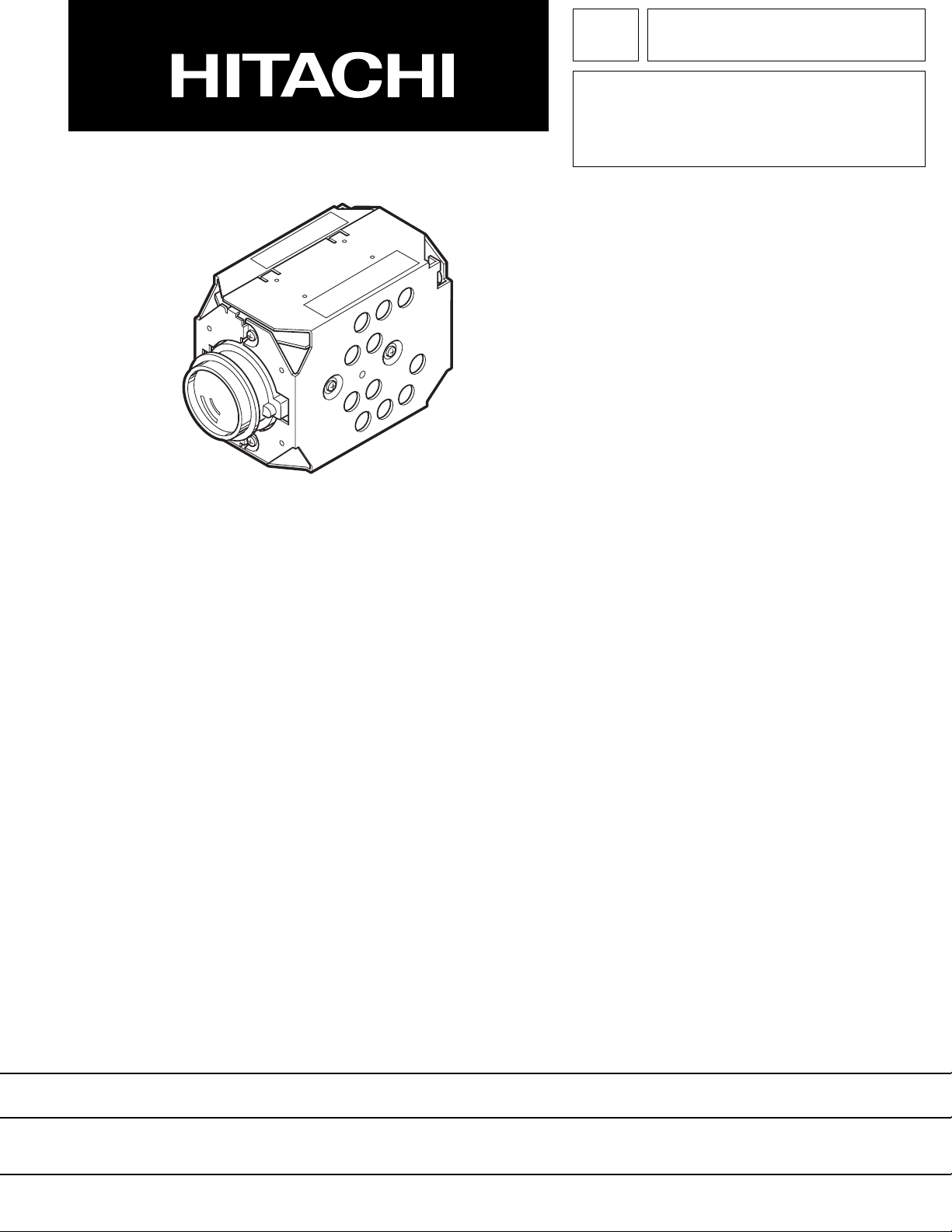
VK-S454
SERVICE MANUAL
VK-S454E
SPECIFICATIONS AND PARTS ARE SUBJECT TO CHANGE FOR IMPROVEMENT
COLOR VIDEO CAMERA
2001January
Digital Media Products Division,Tokai
Page 2

PRODUCT SAFETY NOTICE
Many electrical and mechanical parts have special safety-related characteristics. These are often not evident from visual
inspection nor can the protection afforded by them necessarily be obtained by using replacement components rated for a
higher voltage, wattage, etc. Replacement parts which have these special safety characteristics are identified in this
Service Manual. Electrical components having such features are identified by marking with a on the schematics and the
parts list in this Service Manual. The use of a substitute replacement component which does not have the same safety
characteristics as the HITACHI recommended replacement one, shown in the parts list in this Service Manual, may create
shock, fire, or other hazards. Product safety is continuously under review and new instructions are issued from time to time.
For the latest information, always consult the current HITACHI Service Manual. A subscription to, or additional copies for,
HITACHI Service Manual may be obtained at a nominal charge from HITACHI SALES CORPORATION.
!
Microsoft, MS, MS-DOS, Windows and Windows NT are registered trademarks of Microsoft Corporation.
Pentium and Celeron are registered trademarks of Intel Corporation.
Manufactured under license from Dolby Laboratories.
"Dolby" and double-D symbol are trademarks of Dolby Laboratories.
Confidential unpublished works. (C) 1992-2001 Dolby Laboratories Inc. All rights reserved.
IBM is registered trademarks of International Business Machines Corporations.
Other company names and product names listed are trademarks or brand names belonging to each company.
CAUTION-1
Page 3
Notes When Using Service Manual
The following shows the contents to be noted when using service manual:
1. Value units used in parts list
Certain symbols are indicated below for value units of
resistors, capacitors and coils in parts list. When you read
them note the following regular indications:
Parts
Resistor
Capacitor
Coil
Indication in list Regular indication
...........................................
KOHM
................................................
UF
................................................
PF
................................................
UH
...............................................
MH
2. Values in schematic diagrams
The values, dielectric strength (power capacitance) and
tolerances of the resistors (excluding variable resistors)
and capacitors are indicated in the schematic diagrams
using abbreviations.
[Resistors]
Item
Value
Tolerance
Power
capacitance
Indication
No indication
...................................................
K
..................................................
M
No indication
(All tolerances other than ±5% are
indicated in schematic diagrams)
No indication
(1/16W for leadless resistors without
indication)
All capacitances other than the above
are indicated in schematic diagrams.
...................................
.............................
............................
±5%
1/8W
k
M
k
µF
pF
µH
mH
3. Identifications of sides A/B in
circuit board diagrams
1) Board having a pattern on one side and parts on both
sides.
Side A: Shows discrete parts, viewed from the pattern
side.
Side B: Shows leadless parts, viewed from the
pattern side.
2) Board having patterns on both sides and parts on
both sides.
Side A: Shows parts and patterns which can be seen
when the case is opened.
Side B: Shows parts and the pattern on the back of
side A.
4. Table for indexing locations of parts
This table shows locations of each part on circuit board
diagrams. The locations are indicated using the guide
scales on the external lines of diagrams.
1) One diagram indicated for each board
Symbol
No.
IC
IC1201
Circuit No.
2) Two diagrams indicated for each board
Parts
Location
Type of part
2 A
Zone "A" on board diagram
Zone "2" on board diagram
[Capacitors]
Item
Value
Dielectric
strength
[Coils]
Item
Value
Indication
No indication
...................................................
P
No indication
(All dielectric strengths other than 50V
are indicated in schematic diagrams)
Indication
....................................................
µ
..................................................
m
.................................
..............................
µF
pF
50V
µH
mH
Symbol
No.
IC
IC1201
Circuit No.
Parts
Location
A - 2 A
A: Shows side A
B: Shows side B
Type of
part
Zone "A" on board
diagram
Zone "2" on board
diagram
CAUTION-2
Page 4

CONTENTS
CHAPTER 1 GENERAL INFORMATION
SPECIFICATIONS .................................................. 1-1
COMPARISON OF SPECIFICATION ..................... 1-2
COMPARISON OF MAIN CONTROL ICs .............. 1-2
CHAPTER 2 DISASSEMBLY
DISASSEMBLY PROCEDURE .............................. 2-1
CHAPTER 3
1. Test Equipment/Jigs Necessary for
Adjustment ...................................................... 3-1
1.1 List of equipment and jigs ....................................... 3-1
1.2 List of charts for Adjustment ................................... 3-1
1.3 Test equipment, etc. ................................................ 3-1
2. Before Starting Adjustment ............................ 3-2
2.1 Connections for adjustment .................................... 3-2
2.2 Notes....................................................................... 3-2
2.3 Setting test equipment ............................................ 3-3
3. List of Adjustment Items................................. 3-4
4. Starting Adjustment Program (SMAP) ........... 3-5
5. Adjustment Procedure .................................... 3-6
5.1 Data initialize .......................................................... 3-6
(1) Data initialize ..................................................... 3-6
5.2 Electronic Volume ................................................... 3-6
(1) CDS Sampling Pulse Adjustment ...................... 3-6
5.3 Adjustment .............................................................. 3-7
(1) Auto Iris Control Adjustment.............................. 3-7
(2) White Balance Adjustment ................................ 3-7
(3) Chroma Gain Adjustment .................................. 3-8
5.4 Autofocus ................................................................ 3-9
(1) Zoom/Focus Tracking Adjustment ..................... 3-9
(2) AF Noise Level Adjustment ............................... 3-9
(3) Check of Zoom Track ....................................... 3-10
5.5 Spot Noise ............................................................ 3-10
(1) Spot Noise Adjustment .................................... 3-10
5.6 IR Control .............................................................. 3-11
(1) IR Control Adjustment ..................................... 3-11
6. Error Message................................................ 3-12
6.1 Error Message of Electrical Volume and
Adjustment ............................................................ 3-12
6.2 Error Message of Autofocus ................................. 3-13
7.3 Error Message of Spot Noise................................ 3-13
7.4 Error Message of IR Control ................................. 3-13
7. Troubleshooting of Autofocus ...................... 3-14
(1) No zoom and focus operation ............................... 3-14
(2) No focus lens operation ........................................ 3-16
(3) No zoom operation................................................ 3-17
(4) No autofocus operation......................................... 3-18
(5) Subject is greatly out-of -focus when zoomed ...... 3-19
ELECTRIC CIRCUIT
ADJUSTMENT
8. Troubleshooting of IR control....................... 3-19
(1) No IR control operation ......................................... 3-20
CHAPTER 4 EXPLODED VIEW
EXPLODED VIEW .................................................. 4-1
CHAPTER 5
MECHANICAL PARTS ........................................... 5-1
ELECTRICAL PARTS ............................................ 5-2
REPLACEMENT
PARTS LIST
SCHEMATIC, CIRCUIT
BOARD AND BLOCK
CHAPTER 6 DIAGRAMS/MICRO-
PROCESSOR PIN
FUNCTION TABLE
INTERNAL WIRING DIAGRAM ............................. 6-1
SCHEMATIC / CIRCUIT
BOARD
SENSOR [SP] .................................... 6-3 / 6-13
PROCESS [PC].................................. 6-5 / 6-11
SWITCHING REGULATOR [CSR] ..... 6-8 / 6-14
WAVEFORMS ........................................................ 6-2
BLOCK DIAGRAMS ............................................ 6-15
MICROPROCESSOR PIN FUNCTION TABLE .... 6-17
CONTENTS
Page 5

CHAPTER 1 GENERAL INFORMATION
SPECIFICATINOS
Note: The specifications are subject to change for improvement without notice.
Signal VK-S454: NTSC Format
VK-S454E: PAL Format
Scanning System 2:1 Interlaced
Image Sensor 4.5 mm Dia. (1/4-inch) CCD Image Sensor
Number of Effective Pixels VK-S454: 724 (H) × 494 (V)
VK-S454E: 724 (H) × 582 (V)
Total Number of Pixels VK-S454: 758 (H) × 504 (V)
VK-S454E: 758 (H) × 592 (V)
Scanning Frequency VK-S454: Horizontal 15.734 kHz
Vertical 59.94 Hz
VK-S454E: Horizontal 15.625 kHz
Vertical 50 Hz
Video Signal Output Composite Signal 1.0 Vp-p
Minimum Required Illumination Standard 3.0 lx
DS shutter 0.2 lx
IRcf OFF 0.02 lx
S/N Ratio 50 dB or more
Horizontal Resolution 470 TV Line or more
Operating Temperature 0 - 60 °C
Operating Humidity 10 - 90 %
Power Input DC 9 V ± 0.5 V
Power Consumption 4.6 W or less
Dimensions 50 (W) × 60 (H) × 89.5 (D) mm
Weight Approx. 230 g
1 - 1
Page 6
COMPARISON OF SPECIFICATION
ITEM
Signal Format
Power Requirements
Power Consumption
Dimensions (W × H × D mm)
Weight
Lens
Operating Temperature/Humidity
Image Sensor
Number of Effective Pixels
Total Number of Pixels
Scanning System
Horizontal Scanning Frequency
Vertical Scanning Frequency
Sync Format
Video Signal Output
S/N Ratio
Horizontal Resolution
Minimum Required Illumination
(Standard)
IR cf Mode
VK-S454/VK-S454E
VK-S454: NTSC
VK-S454E: PAL
DC 9 V
4.6 W (MAX)
50 × 60 × 89.5
Approx. 230 g
Power zoom × 23 (3.6 - 82.8 mm)
F 1.6 - 3.7
0 °C to 60 °C
(Recommendation: 0 °C to 40 °C)
10 % to 90 %
4.5mm Dia. (1/4 inch) CCD
VK-S454: 724 (H) × 494 (V)
VK-S454E: 724 (H) × 582 (V)
VK-S454: 758 (H) × 504 (V)
VK-S454E: 758 (H) × 592 (V)
2:1 Interlaced
VK-S454: 15.734 kHz
VK-S454E: 15.625 kHz
VK-S454: 59.94 Hz
VK-S454E: 50 Hz
Internal/External
Composite Signal 1.0 Vp-p
50 dB or more
470 TV Line or more
3.0 lx
Provided
VK-S234/VK-S234E
VK-S234: NTSC
VK-S234E: PAL
3.3 W (MAX)
Power zoom × 22 (4.0 - 88.0 mm)
F 1.6 - 3.8
VK-S234: 768 (H) × 494 (V)
VK-S234E: 752 (H) × 582 (V)
VK-S234: 811 (H) × 508 (V)
VK-S234E: 795 (H) × 596 (V)
VK-S234: 15.734 kHz
VK-S234E: 15.625 kHz
VK-S234: 59.94 Hz
VK-S234E: 50 Hz
VK-S234: 470 TV Line or more
VK-S234E: 460 TV Line or more
Not Provided
COMPARISON OF MAIN CONTROL ICs
ITEM
CCD Sensor
Sensor Drive
Buf. Amp
CDS AGC & A/D CONV.
Camera Digital Signal Processor (DSP)
SD RAM
Inv.
Clock Generator
Digital µP
EEPROM
Reset Pulse Gen.
Zoom Motor Drive
Focus Motor Drive
IR Filter Drive
F.Det./Iris Drive
PWM
Y/C Mix. & Video Amp
Level Shift
VCO/Phase Compa.
FV Pulse Gen.
Inv.
NTSC/PAL Switch
1 - 2
VK-S454: ICX216AN (IC1001)
VK-S454E: ICX217AN (IC1001)
µPD16510GR (IC1002)
HD74AC244 (IC1003)
HD49325BHF (IC1101)
HG75C015ABT (IC1121)
µPD456323G5-A10BL-9JH (IC1150)
TC7SHU04FU (IC1171)
MJU6321P (IC1173)
VK-S454 Series µP (IC1201)
X25097V1-2.7 (IC1250)
RN5VD27AA (IC1251)
TC7S08FU (IC1206)
MPC17AT85VMEL (IC1301)
MPC17AT85VMEL (IC1302)
MPC17AT85VMEL (IC1380)
µPD5023GS-147-GJG (IC1351)
TL1464IPT (IC1501)
BA7664FV (IC1601)
HD74HCT125T (IC1602)
74VHC4046MTCX (IC1603)
TC7S08 (IC1604)
TC7SHU04FU (IC1605)
NJM2533V (IC1606)
VK-S454/VK-S454E
VK-S234/VK-S234E
VK-S234: ICX208AK (IC1001)
VK-S234E: ICX209AK (IC1001)
Not provided
HD49323AF (IC1101)
HG73C053FE (IC1121)
MSM51V18165BSL-6TS-K (IC1122)
TC7SU04F (IC1173)
TC7SU04F (IC1174)
HD6432237M09TE (IC1201)
X25097V1-2.7 (IC1202)
RN5VD27AA (IC1203)
Not provided
Not provided
Not provided
Page 7
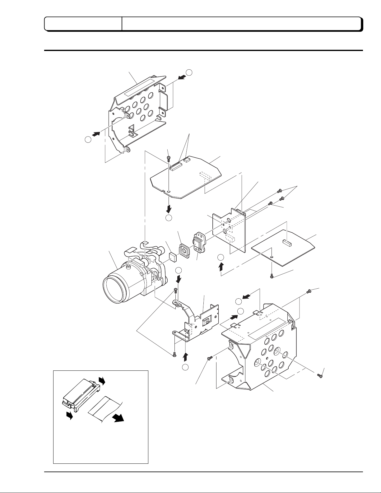
CHAPTER 2 DISASSEMBLY
PROCEDURE
C
LENS
BLOCK
BRACKET-R
(5)
REMOVE
ONE
SCREW
A
RUBBER
CRYSTAL
FILTER
D
(4)
DISCONNECT
TWO FLAT
CABLES (*1)
(9)
UNSOLDER
FOURTEEN
POINTS
CCD
SENSOR
A
BRACKET
PC CIRCUIT
BOARD
B
D
C
SP CIRCUIT
BOARD
(8)
REMOVE
TWO
SCREWS
(7)
(6)
REMOVE
ONE
SCREW
REMOVE
TWO
SCREWS
(*2)
CSR
CIRCUIT
BOARD
(2)
REMOVE
TWO
SCREWS
(10)
REMOVE
THREE
SCREWS
(1)
(1)
(1) Release the lock of the connector
on the left and right.
(2) Pull out the flat cable
(2)
Fig. 2-1-1
(1)
B
REMOVE
TWO
SCREWS
Fig. 2-1
(3)
REMOVE
TWO
SCREWS
BRACKET-L
*1: Do not the pull out the flat cable or touch the exposed
terminal at the connecting position with your bare
hands as it could cause a defective (1) and (2) shown
in Fig. 2-1-1.
*2: When the SP circuit board is removed, the crystal filter
and rubber are also removed.
Be careful not to damege and lose them.
2 - 1
Page 8
CHAPTER 3 ELECTRIC CIRCUIT ADJUSTMENT
1. Test Equipment/Jigs Necessary for Adjustment
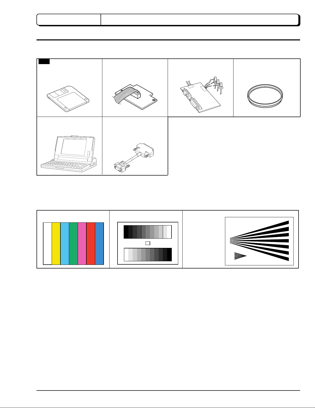
1.1 List of equipment and jigs
New
Adjutsment Floppy
Disk (
*1
)
Personal Computer (PC)
[Goods on the Market]
DSP Interface Connect Jig
No. 7069179
Personal Computer Cable
RS-232C (9 or 25 pins)
Straight Type
[Goods on the Market]
1.2 List of charts for adjustment
DSP-R Jig
No.7099448
*1
: The adjustment floppy disk is not for sale: It will be
supplied only when service maintenance contract
is concluded.
C12 Light Balancing Filter
No.7099369
Color Bar Chart Gray Scale Chart Backfocus Chart
1.3 Test equipment, etc.
Color video monitor (color TV for monitoring)
Oscilloscope
Vectorscope [If not available, adjustment is still possible, but easier if this is used]
Digital voltmeter (DVM)
3100 K light box
DC power supply (9 V/3 A) [To power of video camera]
DC power supply (5 V/1 A) [To power of DSP-R jig]
3 - 1
Page 9
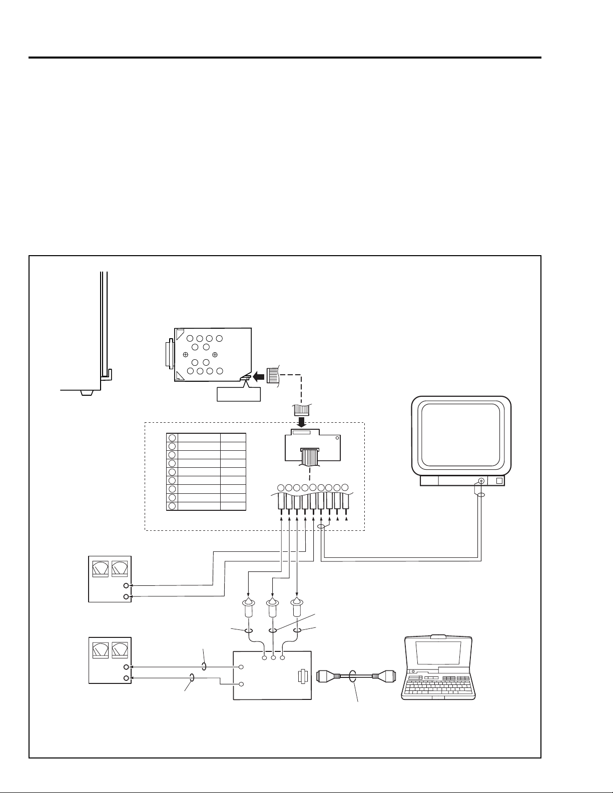
2. Before Starting Adjustment
2.1 Connections for adjustment
Connect the video camera to the test equipment and jigs as shown in Fig. 2-1.
2.2 Notes
1) All adjustments are performed using the adjustment program and personal computer (PC). The adjustment program is
subject to change without notice for improvements in functions and operability, and the actual instructions on PC screen
may be different from those in this manual: If so, follow the instructions on PC screen to proceed with adjustment.
2) The adjustment program will not operate normally unless the video camera, PC and test equipment/jigs are all turned on.
3) Be sure to connect the video output of video camera to a color video monitor (terminate the video output with 75 ohm:
If the video output is not connected to the monitor (and if it is not terminated with 75 ohm), the output video signal level
cannot be measured correctly.
LIGHT
BOX
DC POWER
SUPPLY
(9V/3A)
+
GND
DC POWER
SUPPLY
(5V/1A)
VIDEO CAMERA
PG1601
DSP INTERFACE CONNECT JIG
1
RD WHT
2
SD BRW
3
GND BRW
4
+B BRW
5
GND BRW
6
VIDEO OUT BRW
7
GND BRW
8
EX. FV BRW
9
GND BRW
YEL
RED
9PIN FLAT CABLE
(ACCESSORY)
9
1
2345
1
6
78
WHT
BLK
COLOR VIDEO
MONITOR
9
VIDEO IN
PERSONAL
COMPUTER
3 - 2
GND
+
BLK
DSP-R JIG
PERSONAL
COMPUTER
CABLE (RS-232C)
Fig. 2-1
Page 10

4) Use light box that does not flicker and whose color temperature is controlled, for adjustment. If an inappropriate light box is
used, precise adjustment will not be possible, and the adjustment program will not operate normally.
5) Take care with the following when pointing the video camera at a chart (light box):
Focus the chart correctly.
Set the chart (light box) 30-50 cm away from the lens surface, and avoid any effects from surrounding light (except for
a case where some designation is given).
Aim at the chart and let chart fill the screen (video period). (Except for a case where some designation is given.)
2.3 Setting test equipment
1) Set the switches, knobs and each mode of oscilloscope as follows for adjustment:
Probe: 10:1
TIME/DIV: 10 or 20 µs (except for a case where some designation is given)
VOLTS/DIV: Will vary depending on the measurement object (except for a case where some designation is
given)
Synchronization: Internal sync (except for a case where some designation is given)
AC/DC/GND: AC (except for a case where some designation is given)
Note: The names of switches, knobs, modes, etc. of oscilloscope may vary slightly depending on the manufacturer or
model. Since some oscilloscopes may have switches, etc. other than the above that must be set, see the instruction
manual of the particular oscilloscope for details.
3 - 3
Page 11
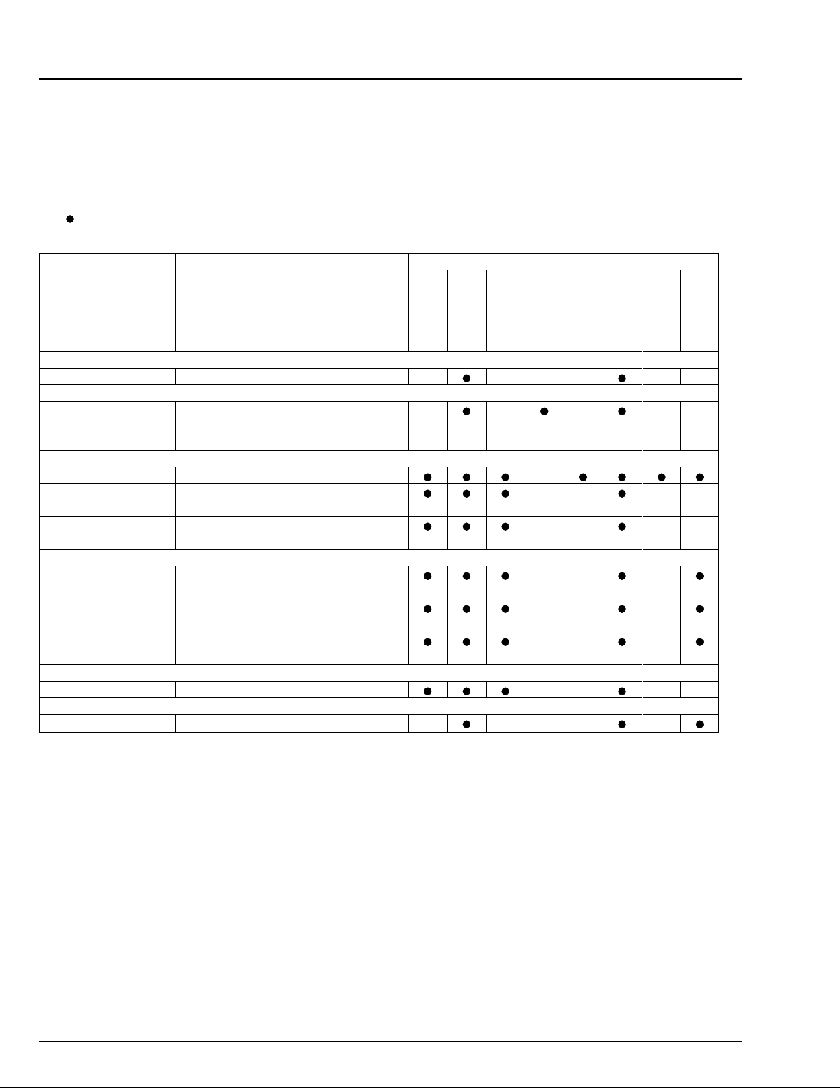
3. List of Adjustment Items
The following table shows the adjustment items, their purposes, and whether or not check is required after replacing major
components.
The components shown in the table below are the minimum to be checked after replacing major components: If several
components have been replaced - or depending on the cause of a defect - more components may need to be checked.
: CHECK
Name of Major Components
Item of Adjustment
Data Initialize
(1) Data Initialize (*2)
Electric Volume
(1) CDS Sampling
Pulse
Adjustment
(1) Auto Iris Control
(2) White Balance
(3) Chroma Gain
Autofocus
(1) Zoom/Focus
Tracking
(2) AF Noise Level
(3) Check of Zoom
Trace
Spot Noise
(1) Spot Noise
IR Control
(1) IR Control
Purpose of Adjustment
Initilizing EEPROM.
To suppress noise in the CCD sensor
output signal and maximize the signal
level.
To set the iris control data.
To input the automatic wihite balance
control data.
To set the color saturation under the
reference color temperature.
To set the out-of -focus correction level
during zooming.
To set the noise level in the autofocus
circuit.
To check the autofocus adjustment.
To correct spot noise.
To set the IR filter control data.
PC circuit
SP circuit
board
IC1001
board (*1)
IC1101
IC1201
IC1250 (*1)
IC1351
Lens Block
*1: When replacing the PC circuit board (containing EEPROM) or EEPROM, be sure to perform all adjustments
only after “Data Initialize”.
*2: Since all adjustments must be performed any time “Data Initialize” is done, do not perform it indiscriminately.
3 - 4
Page 12

4. Starting Adjustment Program (SMAP)
CAN NOT FIND THE DATA FILE
**** PRESS ANY KEY ****
***********************************************************
MANUAL ADJUSTMENT PROGRAM
***********************************************************
[A] DATA INITIALIZE
[B] ELECTRIC VOLUME
[C] ADJUSTMENT
[D] AUTO FOCUS
[E] SPOT NOISE
[F] IR CONTROL
[ESC] END
Please select [A] - [F] or [ESC]
Note: If error message appears during adjustment, refer to “6. Error Messages”.
1) Connect the video camera, DSP-R jig and PC as shown in Fig. 2-1, and supply power to them. (*1)
2) Operate the PC to start MS-DOS . (*2)
R
3) Make sure that the adjustment floppy disk is write-protected.
4) Insert the adjustment floppy disk into the floppy disk drive of PC.
5) Use the PC keyboard to type A:. (*3) (See the MS-DOS screen)
6) Type SMAP_IBM (space) 1. (*4) (See the SMAP input screen)
R
7) The SMAP will start: Make sure that the model select screen appears on the PC display. (*5) (See the model select
screen)
8) If the appropriate model is displayed on the model select screen, input the number to PC. If the appropriate model name is
not shown on the model select screen, input P to PC until the model name appears. (*6)
9) The screen for verifying the model name will appear on PC display: If it is correct, input Y to PC. If it is incorrect, input N
and start over (from step 8).
10)Make sure that the main menu appears on PC display: If it does not appear, check whether model selection (in step 8) is
correct.
*1: If the connection of jig, etc. is inappropriate or power is not supplied, the adjustment program will not start normally.
*2: For details on how to start MS-DOS, refer to the instruction manual of PC, since this varies for each PC.
*3: The letter to be input is to designate the drive into which the adjustment floppy disk has been inserted. If using a drive
other than A, designate the drive.
*4: The number to be input after a space is to designate the serial port no. of PC. If the PC has two or more serial ports,
and the DSP-R jig is connected to a port other than serial port 1, input the serial port no.
*5: If the model select screen does not appear, make sure of the following:
Power is supplied to the video camera and DSP-R jig.
The designation of drive (in step 5) is correct.
The designation of serial port is correct.
The correct adjustment floppy disk has been correctly inserted.
*6: If an erroneous model name or number is selected, misoperation message will appear on PC display: Press any key to
restore the model select screen.
To terminate the adjustment program (SMAP):
Press the [Esc] key once to three times until the PC display returns from each menu screen to the MS-DOS screen.
When the MS-DOS screen appears on PC display, turn off the video camera and jig.
PC Display & Figs
MS-DOS screen
C>A:
A>
SMAP input screen
C>A:
A>SMAP_IBM 1
Model select screen
***********************************************************
***********************************************************
MODEL SELECT
[1] ЧЧЧЧЧЧЧЧ
[2] ЧЧЧЧЧЧЧЧ
[3] ЧЧЧЧЧЧЧЧ
[4] ЧЧЧЧЧЧЧЧ
[5] ЧЧЧЧЧЧЧЧ
[P] NEXT SELECTION
[ESC] END
Please select the type of the set
Press [1] - [5] or [P] or [ESC]
Screen for verifying model name
Selected model is ЧЧЧЧЧЧЧЧ
Are you sure ? (Y/N)
Main menu
Misoperation message
3 - 5
Page 13

5. Adjustment Procedure
The following explains the adjustment procedure using the adjustment program (SMAP), following the order of items on the
main menu screen.
Refer to “4. Starting Adjustment Program (SMAP)” in advance, start SMAP and display the main menu on PC display.
In actual work, it is possible to adjust one item independently.
Note: If error message appears on PC display during adjustment, perform troubleshooting, referring to “6. Error Messages”.
5.1 Data Initialize
(1) Data Initialize
This procedure initializes the data in EEPROM (including the adjustment data). Any time you replace the PC circuit board
(containing EEPROM), be sure to perform this procedure. [Generally, this procedure is not necessary after replacing other
circuit board (components).]
Important:
After completing this adjustment, be sure to perform all adjustment items as follows.
Procedure:
1) Input A to PC on the main menu screen.
2) The screen for verifying the initialization will appear: Input Y to PC. (*1)
3) Follow the instructions on PC display thereafter.
*1: Entering N on the screen for verifying initialization will restore the data main menu screen.
5.2 Electronic Volume
Before starting:
1) Input B to PC on the main menu screen to display the electronic volume menu screen.
2) Input to PC the appropriate adjustment number. (*1)
*1: Pressing the [Esc] key on the adjustment menu screen will restore the main menu screen.
(1) CDS Sampling Pulse Adjustment
Incompleted Phenomenon:
Diagonal beats and horizontal noise occure.
Procedure:
1) Input 1 to PC on the adjustment menu screen.
2) Follow the instruction on PC display thereafter.
PC Display & Figs
Main menu Screen for verifying initialization
***********************************************************
MANUAL ADJUSTMENT PROGRAM
***********************************************************
[A] DATA INITIALIZE
[B] ELECTRIC VOLUME
[C] ADJUSTMENT
[D] AUTO FOCUS
[E] SPOT NOISE
[F] IR CONTROL
[ESC] END
Please select [A] - [F] or [ESC]
<< DATA WRITING >>
START TO SEND DATA. (Y/N)
3 - 6
Electronic volume menu
***********************************************************
***********************************************************
ELECTRIC VOLUME
[1] CDS SAMPLING PULSE
[ESC] RETURN TO MAIN MENU
Please select [1] or [ESC]
Page 14

5.3 Adjustment
ADJUSTMENT FINISHED
PRESS ANY KEY
<< ADJUSTMENT OF WHITE BALANCE >>
ADJUSTMENT FINISHED
PRESS ANY KEY
Before starting:
1) Input C to PC on the main menu screen to display the adjustment menu screen.
2) Input to PC the appropriate adjustment number. (*1)
*1: Pressing the [Esc] key on the adjustment menu screen will restore the main menu screen.
(1) Auto Iris Control Adjustment
Incompleted Phenomenon:
The picture becomes too bright.
The picture becomes too dark.
Condition:
Set the zoom to wide end and point at the light box, without chart inserted, to fill the screen.
Procedure:
1) Input 1 to PC on the adjustment menu screen.
2) Follow the instruction on PC display thereafter.
3) After the AIC (auto iris control) adjustment complete screen appears, press any key to restore the adjustment menu
screen.
4) Turn the video camera off, leave as is for at least 5 seconds, and then turn it on again. (*1)
*1: When the video camera is turned on again, the SMAP may not operate normally, and the following
adjustments may not be possible. If this happens, press the [Esc] key to restore the MS-DOS screen, and then
restart the SMAP.
(2) White Balance Adjustment
Incompleted Phenomenon:
Color of the subject is different from that of the picture.
A white subject is not senn as white.
Conditions:
Attach a C12 filter.
Set the zoom to wide end, and point at a gray scale chart.
Procedure:
1) Input 2 to PC on the adjustment menu screen.
2) Follow the instructions on PC display thereafter.
3) After the white balance adjustment complete screen appears, press any key to restore the adjustment menu
screen.
PC Display & Figs
Main menu
***********************************************************
MANUAL ADJUSTMENT PROGRAM
***********************************************************
[A] DATA INITIALIZE
[B] ELECTRIC VOLUME
[C] ADJUSTMENT
[D] AUTO FOCUS
[E] SPOT NOISE
[F] IR CONTROL
[ESC] END
Please select [A] - [F] or [ESC]
Adjustment menu
***********************************************************
***********************************************************
ADJUSTMENT
[1] AUTO IRIS CONTROL
[2] WHITE BALANCE
[3] CHROMA GAIN
[ESC] RETURN TO MAIN MENU
Please select [1] - [3] or [ESC]
AIC adjustment complete
White balance adjustment complete
3 - 7
Page 15

(3) Chroma Gain Adjustment (Figs. 5-1, 5-2, 5-3)
Incompleted Phenomenon:
Color of the picture is denser than that of the subjuct.
Color of the picture is lighter than that of the subject.
Equipment:
Oscilloscope or Vectorscope
Test Point:
Video Out (PG1601-6)
Condition:
Atach a C12 filter
Point the at a color bar chart.
Procedure:
1) Input 3 to PC on the adjustment menu screen.
2) The chroma gain adjustment screen will appear.
3) When using an oscilloscope (Fig. 5-1):
Press the D or U key to set the red level on waveform to approx. 620 mVp-p.
Then, while holding down the [Ctrl] key, press the D or U key to set the red level on waveform to approx.
620 mV ± 20 mVp-p.
When using a vectorscope (Figs. 5-2, 5-3):
Press the D or U key to set the red vector to approx. 220% of burst vector.
Then, while holding down the [Ctrl] key, press the D or U key to set the red vector to approx. 220% ± 5% of
burst vector.
4) Press the [Enter] key: The PC display will switch from the chroma gain data write screen to chroma gain
adjustment complete screen.
5) Press any key to restore the adjustment menu screen.
PC Display & Figs
Adjustment menu
***********************************************************
***********************************************************
Chroma gain adjustment
<< ADJUSTMENT OF CHROMA GAIN >>
[U] CHROMA GAIN UP
[D] CHROMA GAIN DOWN
[Crt] + [U] CHROMA GAIN UP
[Crt] + [D] CHROMA GAIN DOWN
[ENTER] SAVE & RETURN TO MENU
[ESC] QUIT
Chroma gain data write
<< ADJUSTMENT OF CHROMA GAIN >>
ADJUSTMENT
[1] AUTO IRIS CONTROL
[2] WHITE BALANCE
[3] CHROMA GAIN
[ESC] RETURN TO MAIN MENU
Please select [1] - [3] or [ESC]
ROUGH ADJUSTMENT
FINE ADJUSTMENT
DATA WRITING INTO EEPROM
Chroma gain adjustment complete
<< ADJUSTMENT OF CHROMA GAIN >>
ADJUSTMENT FINISHED
PRESS ANY KEY
RED
BURST
100 %
220 %
± 5 %
RED
620 mV
± 20 mV
Fig. 5-1
RED
BURST
220 %
± 5 %
100 %
3 - 8
Fig. 5-2 Fig. 5-3
Page 16

5.4 Autofocus
Before starting adjustment:
1) Input D to PC on the main menu screen to display the AF menu screen.
2) Input the appropriate adjustment number to PC. (*1)
*1: Pressing the [Esc] key on the AF menu screen will restore the main menu screen.
(1) Zoom/Focus Tracking Adjustment
Incompleted Phenomenon:
Focus is lost during zooming.
Condition:
Point at the backfocus chart, 1500 ± 5mm away from the lens surface.
Light the backfocus chart with 200 - 400 lx.
Caution when Adjustment:
1) Measure the distance between the chart and lens surface precisely.
2) Place the chart as parallel as possible to the lens surface.
3) The backfocus chart should always be at the center of the monitor screen when the zoom is set to the wide-angle
and telephoto ends.
4) The zoom trace adjustment procedure is completed within 2 minutes after it is selected.
5) Do not place any obstruction between the lens and chart during adjustment.
Procedure:
1) Input 1 to PC on the AF menu screen.
2) Follow the instructions on PC display thereafter.
(2) AF Noise Level Adjustment
Incompleted Phenomenon:
It takes time until a subject is brought into focus.
Correct focus is not obtained.
Condition:
Point at a light box without a chart inserted at a distance of up to 10cm.
Caution when Adjustment:
1) Place the light box as parallel as possible to the lens surface.
2) The AF noise level adjustment procedure will be completed within thirty seconds after it is selected.
Procedure:
1) Input 2 to PC on the AF menu screen.
2) Follow the instructions on PC display thereafter.
PC Display & Figs
Main menu
***********************************************************
MANUAL ADJUSTMENT PROGRAM
***********************************************************
[A] DATA INITIALIZE
[B] ELECTRIC VOLUME
[C] ADJUSTMENT
[D] AUTO FOCUS
[E] SPOT NOISE
[F] IR CONTROL
[ESC] END
Please select [A] - [F] or [ESC]
AF menu
***********************************************************
***********************************************************
[1] ADJUSTMENT OF ZOOM/FOCUS TRACKING
[2] ADJUSTMENT OF AF NOISE LEVEL
[3] CHECK OF ZOOM TRACE
[ESC] RETURN TO MENU
AUTO FOCUS ADJUSTMENT
Please select [1] - [3] or [ESC]
3 - 9
Page 17

(3) Check of Zoom Trace
Incompleted Phenomenon:
Focus is lost during zooming.
Condition:
Point at the backfocus chart, 1500 ± 5mm away from the lens surface.
Light the backfocus chart with 200 - 400 lx.
Caution when Adjustment:
1) Measure the distance between the chart and lens surface precisely.
2) Place the chart as parallel as possible to the lens surface.
3) The backfocus chart should always be at the center of the monitor screen when the zoom is set to the wide-angle
and telephoto ends.
4) Do not place any obstruction between the lens and chart during adjustment.
Procedure:
1) Input 3 to PC on the AF menu screen.
2) Follow the instructions on PC display thereafter.
If error message appears, readjust the following items:
(1) Zoom/Focus Tracking Adjustment
(2) AF Noise Level Adjustment
5.5 Spot Noise
Important:
Spot noise refers to bright points that appear on the screen, which are caused by a defect in pixel of CCD image sensor.
Perform this adjustment after specified components have been replaced (see “List of Adjustment Items”).
Perform this adjustment if spot noise occurs under abnormal usage conditions or after long-term use.
If spot noise still occurs after this adjustment is complete, the CCD image sensor may be defective.
Perform this adjustment after completing all other adjustments. (Perform this adjustment in normal video status.)
(1) Spot Noise Adjustment
Incompleted Phenomenon:
Spot noise occurs under abnormal usage conditions or after long-term use.
Equipment:
Color video monitor (CRT type is desirable)
Condition:
Cap the lens (so that no light enters).
PC Display & Figs
Main menu
***********************************************************
MANUAL ADJUSTMENT PROGRAM
***********************************************************
[A] DATA INITIALIZE
[B] ELECTRIC VOLUME
[C] ADJUSTMENT
[D] AUTO FOCUS
[E] SPOT NOISE
[F] IR CONTROL
[ESC] END
Please select [A] - [F] or [ESC]
AF menu
***********************************************************
***********************************************************
[1] ADJUSTMENT OF ZOOM/FOCUS TRACKING
[2] ADJUSTMENT OF AF NOISE LEVEL
[3] CHECK OF ZOOM TRACE
[ESC] RETURN TO MENU
AUTO FOCUS ADJUSTMENT
Please select [1] - [3] or [ESC]
3 - 10
Page 18

Procedure:
FINISHED WRITING DATA
PRESS ANY KEY
1) Input E to PC on the main menu screen.
2) Follow the instructions on PC display thereafter.
3) The screen for verifying writing of spot noise data will appear: Input Y. (*1)
4) When writing data is complete, the spot noise data write complete screen will appear: Press any key to restore the
main menu screen.
*1: Entering N on the screen for verifying writing of spot noise data will restore the main menu screen.
5.6 IR Control
(1) IR Control Adjustment
Condition:
Cap the lens (so that no light enters).
Procedure:
1) Input F to PC on the main menu screen.
2) Follow the instructions on PC display thereafter.
3) After the IR control adjustment complete screen appears, press any key to restore the adjustment menu screen.
Main menu
***********************************************************
MANUAL ADJUSTMENT PROGRAM
***********************************************************
[A] DATA INITIALIZE
[B] ELECTRIC VOLUME
[C] ADJUSTMENT
[D] AUTO FOCUS
[E] SPOT NOISE
[F] IR CONTROL
[ESC] END
Please select [A] - [F] or [ESC]
PC Display & Figs
Screen for verifying writing of spot noise data
<< DATA WRITING >>
START TO SEND DATA. (Y/N)
Spot noise data write complete
FINISHED WRITING DATA
PRESS ANY KEY
IR control adjustment complete
3 - 11
Page 19

6. Error Message
A message may appear while you are adjusting the video camera. If a message appears, refer to the following table and take
appropriate corrective action.
6.1 Error Message of Electric Volume and Adjustment
ERROR MESSAGE COUNTERMEASURE
ERROR OCCURRED. IRIS TROUBLE
PRESS ANY KEY
ERROR OCCURRED ON da× ADJUSTMENT
PRESS ANY KEY Defective soldering, damage to pattern, etc. in the above circuit.
D RANGE OVER. ERROR ON da× ADJUSTMENT
PRESS ANY KEY. Defective soldering, damage to pattern, etc. in theabove circuit.
ERROR OCCURRED ON da0 and
da1 ADJUSTMENT circuits.
PRESS ANY KEY Defective soldering, damage to pattern, etc. in the above circuits.
FILE NOT FOUND !!!!
PRESS ANY KEY Check the adjustment floppy disk and replace it if necessary.
FILE OPEN ERROR !!!!
PRESS ANY KEY Check the adjustment floppy disk and replace it if necessary.
ERROR OCCURRED ON C DUTY ADJUSTMENT
PRESS ANY KEY Defective soldering, damage to pattern, etc. in the above circuit.
ERROR OCCURRED ON FDET ADJUSTMENT
PRESS ANY KEY
ERROR OCCURRED. ZOOM DOES NOT WORK
PRESS ANY KEY
TOO BRIGHT
PRESS ANY KEY Move the camera further away from the light box.
TOO DARK
PRESS ANY KEY
D RANGE OVER ERROR ON HALL AMP
IRIS CANNOT OPEN ANY MORE
PRESS ANY KEY
STAURATION ERROR. TOO BRIGHT
PRESS ANY KEY Move the camera further away from the light box.
CAN'T ADJUST WHITE BALANCE
PLEASE RETRY
PRESS ANY KEY
Check whether or not power is supplied.
Check the values of the iris drive circuit.
Defective soldering, damage to pattern, etc. in the above circuit.
Check the iris block and replace it if necessary.
Check the values in the hall amp circuit.
Check the values in the hall amp circuit.
Check the values in the hall amp circuit and its peripheral
The adjustment program (file) cannot be found.
The adjustment program (file) does not start.
Check the values of the iris drive circuit.
Supply power again and re-adjust.
Check the values in the hall amp circuit.
Defective soldering, damage to pattern, etc. in the above circuit.
Supply power again and re-adjust.
The subject is too bright.
The subject is too dark.
Check the light box.
Move the camera closer to the light box.
Supply power again and re-adjust.
The subject is too dark.
Check the light box.
Move the camera closer to the light box.
Check the values in the hall amp circuit.
Defective soldering, damage to pattern, etc. in the above circuit.
The subject is too bright.
The subject is too bright or too dark.
Check the light box.
Move the camera closer to or away from the light box.
Supply power again and re-adjust.
3 - 12
Page 20

6.2 Error Message of Autofocus
ERROR MESSAGE COUNTERMEASURE
ERROR OCCURRED. ZOOM DOES NOT WORK
PRESS ANY KEY
TIME OUT ERROR ON FOCUS
TIME OUT ERROR ON ZOOM
TIME OUT ERROR ON AF STEP
AF LIMIT OVER
AF ERROR
TOO DARK
Supply power again and re-adjust.
Check the conditions of subject.
If this error message appears even when the adjustment is
performed 2 or 3 times, the autofocus circuit system is defective.
Refer to (1) of TROUBLESHOOTING OF AUTOFOCUS.
If this error message appears even when the adjustment is
performed 2 or 3 times, the autofocus circuit system is defective.
Refer to (2) of TROUBLESHOOTING OF AUTOFOCUS.
Check the conditions of subject.
If this error message appears even when the adjustment is
performed 2 or 3 times, the autofocus circuit system is defective.
Refer to (1) of TROUBLESHOOTING OF AUTOFOCUS.
Check the conditions of subject.
If this error message appears even when the adjustment is
performed 2 or 3 times, the autofocus circuit system is defective.
Refer to (2) of TROUBLESHOOTING OF AUTOFOCUS.
If this error message appears even when the adjustment is
performed 2 or 3 times, the autofocus circuit system is defective.
Refer to (1) of TROUBLESHOOTING OF AUTOFOCUS.
Insufficient lighting. Check the subject.
6.3 Error Message of Spot Noise Adjustment
ERROR MESSAGE COUNTERMEASURE
ERROR!!
SPOT NOISE COMPENSATION IS EEPROM.
STOPPED BY INITIAL DATA.
PLEASE CHECK THE EEPROM.
PRESS ANY KEY. Check the EEPROM, and if necessary, replace it.
ERROR!!
THRESHOLD DATA ERROR.
PLEASE CHECK THE EEPROM.
PRESS ANY KEY.
ERROR!!
THE SPOT NOISE IS TOO MANY. limit.
CAN'T COMPENSATE ANY MORE.
PRESS ANY KEY.
Spot noise compensation is inhibited by the data in the
Turn the power on again.
Data in the EEPROM is defective. (Initialize it.)
Turn the power on again.
Data in the EEPROM is defective. (Initialize it.)
Check the EEPROM, and if necessary, replace it.
The amount of spot noise that can be compensated reaches the
Turn the power on again.
Check the CCD image sensor, and if necessary, replace it.
6.4 Error Message of IR Control
ERROR MESSAGE COUNTERMEASURE
IR ERROR
If this error message appears even when the adjustment is
performed 2 or 3 times, the IR control circuit system is defective.
Refer to TROUBLESHOOTING OF IR CONTROL.
3 - 13
Page 21

7. Troubleshooting of Autofocus
1
Check the connections
of the lens flat cable.
TL1346:3V
TL1335:PULSE
Lens block faulty
IC1201 faulty.
R1203 faulty.
Q1201 faulty.
Check the 3V line
Correct the connections
of the cable.
NG
OK
OK
OK
OK
OK
NG
NG
NG
NG
2
IC1301-3:PULSE
IC1301-4:PULSE
Check IC1301
3
IC1201 faulty.
IC1201 faulty.
OK
NG
IC1301-30:PULSE
IC1201 faulty.
L1301 faulty
NG
(1) NO ZOOM AND FOCUS OPERATION
3 - 14
OK
TL1301:8V
EEPROM
Check IC1201 and
Lens block faulty.
1
NG
TL1345:PULSE
When power turned on:
OK
OK
TL1331-TL1334:PULSES
Check the 5V line
NG
NG
OK
IC1301-2,10,29:5V
Check the 8V line
NG
IC1301-12,20:8V
IC1201 faulty
NG
OK
IC1301-28:PULSE
OK
2
Page 22

Lens block faulty.
4
Check the connections
of the lens flat cable.
TL1346:3V
TL1344:PULSE
Lens block faulty.
IC1201 faulty.
R1204 faulty.
Q1201 faulty.
Check the 3V line
Correct the connections
of the flat cable.
NG
NG
NG
OK
OK
OK
4
Check the 5V line
Check the 8V line.
IC1201 faulty.
IC1201 faulty.
IC1201 faulty.
NG
3
When power turned on:
TL1336:PULSE
OK
OK
NG
TL1347-TL1350:PULSES
NG
IC1302-2,10,29:5V
NG
OK
IC1302-12,20:8V
NG
OK
IC1302-28:PULSE
NG
OK
OK
IC1302-3:PULSE
NG
OK
IC1302 faulty.
IC1302-30:PULSE
3 - 15
Page 23

See "(1)No zoom and
1
OK
OK
OK
NG
NG
NG
Check the connections
of the lens flat cable
TL1346:3V
TL1344:PULSE
Lens block faulty.
IC1201 faulty.
R1204 faulty.
Q1201 faulty.
Check the 3V line
Correct the connections
of the flat cable.
focus operation."
1
Lens block faulty.
Check the 5V line
Check the 8V line
IC1201 faulty.
IC1201 faulty.
IC1201 faulty.
NO
normally?
Does zoom operate
(2) NO FOCUS LENS OPERATION
3 - 16
NG
YES
When power turned on:
OK
OK
TL1345:PULSE
TL1347-TL1350:PULSES
NG
NG
IC1302-2,10,29:5V
NG
OK
NG
OK
IC1302-12,20:8V
IC1302-28:PULSE
NG
OK
IC1302-3:PULSE
NG
OK
OK
IC1302-30:PULSE
OK
IC1302 faulty.
Page 24

See "(1) No zoom and
1
Check the connections
of the lens flat cable.
TL1346:3V
TL1335:PULSE
Lens block faulty.
2
IC1301-3:PULSE
IC1301-4:PULSE
IC1301 faulty
Correct the connections
of the flat cable.
Check the 3V line
IC1201 faulty.
R1203 faulty.
Q1201 faulty.
IC1201 faulty.
IC1201 faulty.
NG
NG
NG
NG
NG
OK
OK
OK
OK
OK
IC1301-30:PULSE
IC1201 faulty.
NG
OK
focus operation."
NO
Zoom switch faulty.
NGCheck the
1
NG
Lens block faulty.
OK
Check the 5V line
NG
Check the 8V line
NG
IC1201 faulty.
NG
(3)NO ZOOM OPERATION
YES
normally?
Does focus operate
zoom switch unit.
OK
EEPROM
Check IC1201 and
OK
TL1336:PULSE
When power turned on:
NG
TL1331-TL1334:PULSES
OK
IC1301-2,10,29:5V
OK
IC1301-12,20:8V
OK
2
IC1301-28:PULSE
3 - 17
Page 25

See "(1) No zoom and
3
TL1346:3V
TL1344:PULSE
Lens block faulty.
IC1201 faulty.
R1204 faulty.
Q1201 faulty.
Check the 3V line
Correct the connections
of the flat cable.
NG
OK
NG
OK
NG
OK
Check the connections
of the lens flat cable.
1
Set the zoom to the
wide-angle end.
Point at the objects
from the infinity to
close-up ends.
Is there a point at
which focus is obtained
between the infinity
and close-up ends?
Check IC1201 and
EEPROM
NO
OK
NG
YES
TL1336:PULSE
2
3
Initialize the unit
and adjust autofocuss.
Does autofocus
operate normally?
IC1201 faulty.
END
NO
YES
Note: For the item marked , perform all
the adjustments required when the
unit is initialized, before
adjusting autofocus.
focus operation."
NO
of the subject.
Increase the illumination
NO
Camera circuit faulty.
NO
YES
Does the video
level increase?
YES
normally?
(4) NO AUTOFOCUS OPRATION
3 - 18
Does zoom operate
YES
to video output
VIDEO SIGNAL:
360mVp-p or more
Connect an oscilloscope
1
Page 26

Lens block faulty.
(5) SUBJECT IS GREATLY OUT-OF-FOCUS WHEN ZOOMED.
NG
NO
NO
OK
Check the Zoom switch
unit.
IC1201-49:1.2-1.6V
Initialize the unit and
adjust autofocus
Does autofocus
operate normally?
END
IC1201 faulty.
D1201,C1206,R1215
faulty.
Zoom switch faulty.
Note: For the item marked , perform all
the adjustments required when the
unit is initialized, before
adjusting autofocus.
YES
YES
Check the 5V line
Check the 8V line
IC1201 faulty.
IC1201 faulty.
IC1201 faulty.
2
OK
TL1347-TL1350:PULSES
NG
NG
IC1302-2,10,29:5V
NG
OK
OK
IC1302-12,20:8V
NG
IC1302-28:PULSE
NG
OK
IC1302-3:PULSE
NG
OK
IC1302-30:PULSE
OK
IC1302 faulty.
3 - 19
Page 27

8. Troubleshooting of IR control
1
Check the connections
of the lens flat cable.
Lens block faulty
Correct the connections
of the cable.
NG
OK
OK
OK
NG
NG
2
IC1380-3:PULSE
IC1380-4:PULSE
IC1201 faulty.
IC1201 faulty.
OK
NG
IC1380-30:PULSE
IC1201 faulty.
IC1380 faulty
L1301 faulty
NG
(1) NO IR CONTROL OPERATION
3 - 20
OK
TL1301:8V
Check IC1201 and
EEPROM
Lens block faulty.
1
NG
TL1381:PULSE
When power turned on:
OK
OK
NG
TL1383-TL1386:PULSES
Check the 5V line
NG
IC1380-2,10,29:5V
Check the 8V line
NG
OK
IC1380-12,20:8V
IC1201 faulty
NG
OK
IC1380-28:PULSE
OK
2
Page 28

CHAPTER 4 EXPLODED VIEW
C
138
D
PC CIRCUIT
908
A
603
BOARD
SP CIRCUIT
BOARD
907
906
CSR CIRCUIT
BOARD
E
D
601
136
906
104
906
602
A
A
C
B
908
913
D
C
137
B
913
909
B
A
1234
4 - 1
Page 29

CHAPTER 5 REPLACEMENT PARTS LIST
1. MECHANICAL PARTS LIST
SYMBOL
NO
002 JP31901 PWB ASSY PC [For VK-S454]
002 JP31902 PWB ASSY PC [For VK-S454E]
104 DT10392 CRYSTAL
136 NA30812 BRACKET
137 NA19622 BRACKET(L)
138 NA19631 BRACKET
601 KQ10861 LENS ASSY
602 NX18521 RUBBER
603 UE15091 CCD IMAGE SENSOR [For VK-S454]
603 UE15092 CCD IMAGE SENSOR [For VK-S454E]
906 7775945 SCREW(2X5)
907 8650103 SCREW(2X3)
908 8650105 SCREW (2X5)
909 8749103 2X3 BIND SCREW
913 7775963 SCREW(2X3)
P-NO DESCRIPTION
MECHANISM SECTION
SYMBOL
NO
P-NO DESCRIPTION
5 - 1
Page 30

2. ELECTRICAL PARTS LIST
SYMBOL
NO
C1001 0893107 CERAMIC CHIP 5.0PF+-0.25% 50V
C1002 AA00393R CHIP CERAMIC 1.0UF+80-20% 50V
C1003 AA00393R CHIP CERAMIC 1.0UF+80-20% 50V
C1004 AA00393R CHIP CERAMIC 1.0UF+80-20% 50V
C1005 AA00393R CHIP CERAMIC 1.0UF+80-20% 50V
C1006 0893213 CERAMIC CHIP 2200PF+-10% 50V
C1007 AA00422R CERAMIC CHIP 10UF 16V
C1008 0893193 CERAMIC CHIP 0.01UF+-10% 25V
C1009 AA01032R CERAMIC CAPACITOR 100000PF+-10% 250V
C1010 AA10383R CHIP CAPACITOR 1UF+-10% 50V
C1011 0893014 CERAMIC CHIP 0.01UF+-10% 25V
C1012 AA00951R CERAMIC CAPACITOR 1.0UF+-10% 16V
C1013 AA00931R CERAMIC CAPACITOR 1.0UF+-10% 10V
C1014 AA00393R CHIP CERAMIC 1.0UF+80-20% 50V
C1015 0893008 CERAMIC CHIP 0.1UF +-10% 16V
C1019 AA00441R CHIP CAPACITOR 22UF+-20% 6.3V
C1020 0893008 CERAMIC CHIP 0.1UF +-10% 16V
C1021 AA00422R CERAMIC CHIP 10UF 16V
C1022 AA00422R CERAMIC CHIP 10UF 16V
C1023 AA00393R CHIP CERAMIC 1.0UF+80-20% 50V
C1024 0893008 CERAMIC CHIP 0.1UF +-10% 16V
C1025 AA00931R CERAMIC CAPACITOR 1.0UF+-10% 10V
C1026 AA00441R CHIP CAPACITOR 22UF+-20% 6.3V
C1027 0893008 CERAMIC CHIP 0.1UF +-10% 16V
C1029 0893008 CERAMIC CHIP 0.1UF +-10% 16V
C1101 AA00931R CERAMIC CAPACITOR 1.0UF+-10% 10V
C1102 0893193 CERAMIC CHIP 0.01UF+-10% 25V
C1103 AA00931R CERAMIC CAPACITOR 1.0UF+-10% 10V
C1104 AA00441R CHIP CAPACITOR 22UF+-20% 6.3V
C1105 AA00931R CERAMIC CAPACITOR 1.0UF+-10% 10V
C1106 AA00381R CERAMIC CHIP 10UF+-10% 6.3V
C1107 0893088 CERAMIC CHIP 0.015UF+-10% 16V
C1108 AA00931R CERAMIC CAPACITOR 1.0UF+-10% 10V
C1109 0893179 CERAMIC CHIP 0.1UF+-10% 16V
C1110 0893179 CERAMIC CHIP 0.1UF+-10% 16V
C1111 0893179 CERAMIC CHIP 0.1UF+-10% 16V
C1112 0893179 CERAMIC CHIP 0.1UF+-10% 16V
C1113 0893179 CERAMIC CHIP 0.1UF+-10% 16V
C1114 0893193 CERAMIC CHIP 0.01UF+-10% 25V
C1115 AA00931R CERAMIC CAPACITOR 1.0UF+-10% 10V
C1125 0893114 CERAMIC CHIP 12PF+-5% 50V
C1126 0893114 CERAMIC CHIP 12PF+-5% 50V
C1131 0893193 CERAMIC CHIP 0.01UF+-10% 25V
C1132 AA00441R CHIP CAPACITOR 22UF+-20% 6.3V
C1133 AA00422R CERAMIC CHIP 10UF 16V
C1134 AA00441R CHIP CAPACITOR 22UF+-20% 6.3V
C1135 AA00422R CERAMIC CHIP 10UF 16V
C1140 AA00931R CERAMIC CAPACITOR 1.0UF+-10% 10V
C1141 AA00931R CERAMIC CAPACITOR 1.0UF+-10% 10V
C1142 AA00931R CERAMIC CAPACITOR 1.0UF+-10% 10V
C1143 0893193 CERAMIC CHIP 0.01UF+-10% 25V
C1144 0893193 CERAMIC CHIP 0.01UF+-10% 25V
C1145 AA00422R CERAMIC CHIP 10UF 16V
C1146 AA00931R CERAMIC CAPACITOR 1.0UF+-10% 10V
C1147 AA00931R CERAMIC CAPACITOR 1.0UF+-10% 10V
C1148 0893193 CERAMIC CHIP 0.01UF+-10% 25V
C1149 0893193 CERAMIC CHIP 0.01UF+-10% 25V
C1150 0893193 CERAMIC CHIP 0.01UF+-10% 25V
C1151 AA01101R CERAMIC CAPACITOR 1UF+80-20% 10V
C1152 AA01101R CERAMIC CAPACITOR 1UF+80-20% 10V
C1153 0893193 CERAMIC CHIP 0.01UF+-10% 25V
C1154 AA00931R CERAMIC CAPACITOR 1.0UF+-10% 10V
P-NO DESCRIPTION
CAPACITORS
SYMBOL
NO
C1155 AA00931R CERAMIC CAPACITOR 1.0UF+-10% 10V
C1156 0893193 CERAMIC CHIP 0.01UF+-10% 25V
C1157 0893193 CERAMIC CHIP 0.01UF+-10% 25V
C1158 0893193 CERAMIC CHIP 0.01UF+-10% 25V
C1159 0893193 CERAMIC CHIP 0.01UF+-10% 25V
C1160 0893193 CERAMIC CHIP 0.01UF+-10% 25V
C1161 0893193 CERAMIC CHIP 0.01UF+-10% 25V
C1162 0893193 CERAMIC CHIP 0.01UF+-10% 25V
C1163 0893193 CERAMIC CHIP 0.01UF+-10% 25V
C1165 AA00931R CERAMIC CAPACITOR 1.0UF+-10% 10V
C1166 0893179 CERAMIC CHIP 0.1UF+-10% 16V
C1167 AA00931R CERAMIC CAPACITOR 1.0UF+-10% 10V
C1168 AA00422R CERAMIC CHIP 10UF 16V
C1170 0893101 CERAMIC CHIP 0.5PF+-0.25% 50V
C1171 0893179 CERAMIC CHIP 0.1UF+-10% 16V
C1172 0893123 CERAMIC CHIP 56PF+-5% 50V
C1173 0893123 CERAMIC CHIP 56PF+-5% 50V
C1174 0893193 CERAMIC CHIP 0.01UF+-10% 25V
C1177 0893179 CERAMIC CHIP 0.1UF+-10% 16V
C1178 0893175 CERAMIC CHIP 1000PF+-5% 50V
C1180 0893108 CERAMIC CHIP 6.0PF+-0.5% 50V
C1181 0893108 CERAMIC CHIP 6.0PF+-0.5% 50V
C1183 0893175 CERAMIC CHIP 1000PF+-5% 50V
C1184 0893179 CERAMIC CHIP 0.1UF+-10% 16V
C1185 AA00422R CERAMIC CHIP 10UF 16V
C1186 0893179 CERAMIC CHIP 0.1UF+-10% 16V
C1201 0893193 CERAMIC CHIP 0.01UF+-10% 25V
C1204 0893179 CERAMIC CHIP 0.1UF+-10% 16V
C1205 0893179 CERAMIC CHIP 0.1UF+-10% 16V
C1206 0893193 CERAMIC CHIP 0.01UF+-10% 25V
C1207 0893193 CERAMIC CHIP 0.01UF+-10% 25V
C1208 0893179 CERAMIC CHIP 0.1UF+-10% 16V
C1209 0893193 CERAMIC CHIP 0.01UF+-10% 25V
C1210 0893193 CERAMIC CHIP 0.01UF+-10% 25V
C1211 0893193 CERAMIC CHIP 0.01UF+-10% 25V
C1215 0893193 CERAMIC CHIP 0.01UF+-10% 25V
C1216 0893177 CAPACITOR 0.068UF+-10% 16V
C1218 0893193 CERAMIC CHIP 0.01UF+-10% 25V
C1220 0893193 CERAMIC CHIP 0.01UF+-10% 25V
C1221 AA00422R CERAMIC CHIP 10UF 16V
C1222 0893193 CERAMIC CHIP 0.01UF+-10% 25V
C1301 0893222 CERAMIC CHIP 0.01UF+-10% 50V
C1302 0893215 CERAMIC CHIP 3300PF+-10% 50V
C1303 0893217 CERAMIC CHIP 4700PF+-10% 50V
C1304 0893217 CERAMIC CHIP 4700PF+-10% 50V
C1305 0893193 CERAMIC CHIP 0.01UF+-10% 25V
C1306 0893222 CERAMIC CHIP 0.01UF+-10% 50V
C1307 0893215 CERAMIC CHIP 3300PF+-10% 50V
C1308 0893217 CERAMIC CHIP 4700PF+-10% 50V
C1309 0893217 CERAMIC CHIP 4700PF+-10% 50V
C1310 0893193 CERAMIC CHIP 0.01UF+-10% 25V
C1311 AA00422R CERAMIC CHIP 10UF 16V
C1312 0893179 CERAMIC CHIP 0.1UF+-10% 16V
C1313 0893179 CERAMIC CHIP 0.1UF+-10% 16V
C1314 AA00422R CERAMIC CHIP 10UF 16V
C1317 0893193 CERAMIC CHIP 0.01UF+-10% 25V
C1318 0893193 CERAMIC CHIP 0.01UF+-10% 25V
C1319 0893193 CERAMIC CHIP 0.01UF+-10% 25V
C1320 0893193 CERAMIC CHIP 0.01UF+-10% 25V
C1351 0893193 CERAMIC CHIP 0.01UF+-10% 25V
C1352 0893193 CERAMIC CHIP 0.01UF+-10% 25V
C1353 0893193 CERAMIC CHIP 0.01UF+-10% 25V
C1354 0893132 CERAMIC CHIP 270PF+-5% 50V
C1355 0893193 CERAMIC CHIP 0.01UF+-10% 25V
C1356 0893007 CERAMIC CHIP 0.082UF+-10% 16V
P-NO DESCRIPTION
5 - 2
Page 31

SYMBOL
NO
C1357 0893013 CERAMIC CHIP 0.22UF+-10% 16V
C1358 0893113 CERAMIC CHIP 10PF+-0.5% 50V
C1359 0893133 CERAMIC CHIP 330PF+-5% 50V
C1360 0893133 CERAMIC CHIP 330PF+-5% 50V
C1361 0893133 CERAMIC CHIP 330PF+-5% 50V
C1362 0893008 CERAMIC CHIP 0.1UF +-10% 16V
C1380 0893222 CERAMIC CHIP 0.01UF+-10% 50V
C1381 0893193 CERAMIC CHIP 0.01UF+-10% 25V
C1382 0893193 CERAMIC CHIP 0.01UF+-10% 25V
C1383 0893215 CERAMIC CHIP 3300PF+-10% 50V
C1384 0893179 CERAMIC CHIP 0.1UF+-10% 16V
C1385 0893217 CERAMIC CHIP 4700PF+-10% 50V
C1386 0893217 CERAMIC CHIP 4700PF+-10% 50V
C1387 0893193 CERAMIC CHIP 0.01UF+-10% 25V
C1388 AA00422R CERAMIC CHIP 10UF 16V
C1501 0206672 CHIP CAPACITOR 10UF+-20% 16V
C1502 0893165 CERAMIC CHIP 180PF+-5% 50V
C1503 0893202 CERAMIC CHIP 330PF+-10% 50V
C1504 0893008 CERAMIC CHIP 0.1UF +-10% 16V
C1505 0893008 CERAMIC CHIP 0.1UF +-10% 16V
C1506 0893013 CERAMIC CHIP 0.22UF+-10% 16V
C1507 0209942 CERAMIC CHIP 100PF+-5% 50V
C1508 0893013 CERAMIC CHIP 0.22UF+-10% 16V
C1510 0893008 CERAMIC CHIP 0.1UF +-10% 16V
C1512 0893008 CERAMIC CHIP 0.1UF +-10% 16V
C1513 0893165 CERAMIC CHIP 180PF+-5% 50V
C1514 0893202 CERAMIC CHIP 330PF+-10% 50V
C1515 0893158 CERAMIC CHIP 56PF+-5% 50V
C1516 0893203 CERAMIC CHIP 390PF+-10% 50V
C1517 0893165 CERAMIC CHIP 180PF+-5% 50V
C1518 0893202 CERAMIC CHIP 330PF+-10% 50V
C1519 0893062 CERAMIC CHIP 1UF+80-20% 16V
C1520 0206671 ELECTROLYTIC 10UF 10V
C1521 0893062 CERAMIC CHIP 1UF+80-20% 16V
C1522 0893062 CERAMIC CHIP 1UF+80-20% 16V
C1523 0206671 ELECTROLYTIC 10UF 10V
C1524 AA00441R CHIP CAPACITOR 22UF+-20% 6.3V
C1525 0893062 CERAMIC CHIP 1UF+80-20% 16V
C1526 0206671 ELECTROLYTIC 10UF 10V
C1527 0893062 CERAMIC CHIP 1UF+80-20% 16V
C1528 0893062 CERAMIC CHIP 1UF+80-20% 16V
C1529 0893062 CERAMIC CHIP 1UF+80-20% 16V
C1530 AA00393R CHIP CERAMIC 1.0UF+80-20% 50V
C1531 0893062 CERAMIC CHIP 1UF+80-20% 16V
C1532 AA00393R CHIP CERAMIC 1.0UF+80-20% 50V
C1601 0893193 CERAMIC CHIP 0.01UF+-10% 25V
C1602 0206671 ELECTROLYTIC 10UF 10V
C1603 0893225 CERAMIC CHIP 0.1UF+80-20% 16V
C1604 0806129 ELECTROLYTIC 22UF 10V
C1605 AD10273R CHIP RESISTOR 100UF+-20% 6.3V
C1606 AD10252R ELECTROLYTIC 1.0UF 20V
C1610 0893179 CERAMIC CHIP 0.1UF+-10% 16V
C1611 0893193 CERAMIC CHIP 0.01UF+-10% 25V
C1612 0893179 CERAMIC CHIP 0.1UF+-10% 16V
C1613 0893011 CERAMIC CHIP 0.15UF+-10% 16V
C1614 AA00951R CERAMIC CAPACITOR 1.0UF+-10% 16V
C1615 0893008 CERAMIC CHIP 0.1UF +-10% 16V
C1616 0893225 CERAMIC CHIP 0.1UF+80-20% 16V
C1617 0893117 CERAMIC CHIP 22PF+-5% 50V
C1618 0893179 CERAMIC CHIP 0.1UF+-10% 16V
C1621 0893114 CERAMIC CHIP 12PF+-5% 50V
C1622 0893179 CERAMIC CHIP 0.1UF+-10% 16V
C1623 0893193 CERAMIC CHIP 0.01UF+-10% 25V
C1624 AA01111R CERAMIC CHIP 1UF 6.3V
C1625 0893179 CERAMIC CHIP 0.1UF+-10% 16V
P-NO DESCRIPTION
SYMBOL
NO
C1626 AA00381R CERAMIC CHIP 10UF+-10% 6.3V
C1650 0893206 CERAMIC CHIP 680PF +-10% 50V
CP1101 5172801 FILTER,LOW PASS
CP1171 BE10501R FILTER
CP1601 BV10211R FILTER
R1001 0790049 CHIP RESISTOR 8.2KOHM+-5% 1/16W
R1002 0103831 CHIP RESISTOR 100 OHM+-5% 0.1W
R1003 0103829 CHIP RESISTOR 68 OHM+-5% 0.1W
R1005 0790064 CHIP RESISTOR 100KOHM+-5% 1/16W
R1020 AQ00196R CHIP RESISTOR 1.2KOHM+-1% 1/16W
R1021 AQ00215R CHIP RESISTOR 6.2KOHM+-1% W/16W
R1101 0790015 CHIP RESISTOR 22 OHM+-5% 1/16W
R1102 AQ00231R CHIP RESISTOR 24KOHM+-1% 1/16W
R1105 0790025 CHIP RESISTOR 120 OHM+-5% 1/16W
R1140 0790059 CHIP RESISTOR 47KOHM+-5% 1/16W
R1143 0790059 CHIP RESISTOR 47KOHM+-5% 1/16W
R1144 AQ00251R RESISTOR 130 OHM+-1%0.063W
R1145 AQ00214R CHIP RESISTOR 5.6KOHM+-1% 1/16W
R1146 0790059 CHIP RESISTOR 47KOHM+-5% 1/16W
R1147 AQ00194R CHIP RESISTOR 1.0KOHM+-1% 1/16W
R1148 AQ00205R CHIP RESISTOR 2.7KOHM+-1% 1/16W
R1149 0790037 CHIP RESISTOR 1KOHM+-5% 1/16W
R1151 AQ00194R CHIP RESISTOR 1.0KOHM+-1% 1/16W
R1155 AQ00194R CHIP RESISTOR 1.0KOHM+-1% 1/16W
R1156 0790037 CHIP RESISTOR 1KOHM+-5% 1/16W
R1157 AQ00198R CHIP RESISTOR 1.5KOHM+-1% 1/16W
R1158 AQ00212R CHIP RESISTOR 4.7KOHM+-1% 1/16W
R1171 0790051 CHIP RESISTOR 10KOHM+-5% 1/16W
R1172 0790059 CHIP RESISTOR 47KOHM+-5% 1/16W
R1173 0790059 CHIP RESISTOR 47KOHM+-5% 1/16W
R1174 0790059 CHIP RESISTOR 47KOHM+-5% 1/16W
R1175 0790077 CHIP RESISTOR 1MOHM+-5% 1/16W
R1177 AQ00194R CHIP RESISTOR 1.0KOHM+-1% 1/16W
R1201 0790027 CHIP RESISTOR 180OHM+-5% 1/16W
R1202 0790055 CHIP RESISTOR 22KOHM+-5% 1/16W
R1203 0790027 CHIP RESISTOR 180OHM+-5% 1/16W
R1204 0790027 CHIP RESISTOR 180OHM+-5% 1/16W
R1205 0790061 CHIP RESISTOR 56KOHM+-5% 1/16W
R1206 0790061 CHIP RESISTOR 56KOHM+-5% 1/16W
R1211 0790055 CHIP RESISTOR 22KOHM+-5% 1/16W
R1212 0790037 CHIP RESISTOR 1KOHM+-5% 1/16W
R1213 0790055 CHIP RESISTOR 22KOHM+-5% 1/16W
R1214 0790037 CHIP RESISTOR 1KOHM+-5% 1/16W
R1215 AQ00223R CHIP RESISTOR 12KOHM+-1% 1/16W
R1216 0790037 CHIP RESISTOR 1KOHM+-5% 1/16W
R1217 0790064 CHIP RESISTOR 100KOHM+-5% 1/16W
R1218 0790064 CHIP RESISTOR 100KOHM+-5% 1/16W
R1219 0790051 CHIP RESISTOR 10KOHM+-5% 1/16W
R1220 0790051 CHIP RESISTOR 10KOHM+-5% 1/16W
R1221 0790051 CHIP RESISTOR 10KOHM+-5% 1/16W
R1222 0790051 CHIP RESISTOR 10KOHM+-5% 1/16W
R1225 0790059 CHIP RESISTOR 47KOHM+-5% 1/16W
R1227 0790055 CHIP RESISTOR 22KOHM+-5% 1/16W
R1228 0790059 CHIP RESISTOR 47KOHM+-5% 1/16W
R1230 0790046 CHIP RESISTOR 4.7KOHM+-5% 1/16W
R1231 0790051 CHIP RESISTOR 10KOHM+-5% 1/16W
R1232 0790031 CHIP RESISTOR 330 OHM+-5% 1/16W
R1233 0790031 CHIP RESISTOR 330 OHM+-5% 1/16W
R1234 0790031 CHIP RESISTOR 330 OHM+-5% 1/16W
R1237 0790031 CHIP RESISTOR 330 OHM+-5% 1/16W
R1238 0790031 CHIP RESISTOR 330 OHM+-5% 1/16W
R1256 0790037 CHIP RESISTOR 1KOHM+-5% 1/16W
P-NO DESCRIPTION
RESISTORS
5 - 3
Page 32

SYMBOL
NO
R1306 0103818 CHIP RESISTOR 8.2OHM+-10% 0.1W
R1307 0103813 CHIP RESISTOR 3.3 OHM+-10% 0.1W
R1308 0790051 CHIP RESISTOR 10KOHM+-5% 1/16W
R1309 0790051 CHIP RESISTOR 10KOHM+-5% 1/16W
R1310 0103818 CHIP RESISTOR 8.2OHM+-10% 0.1W
R1311 0103813 CHIP RESISTOR 3.3 OHM+-10% 0.1W
R1313 0103813 CHIP RESISTOR 3.3 OHM+-10% 0.1W
R1314 0103818 CHIP RESISTOR 8.2OHM+-10% 0.1W
R1315 0790051 CHIP RESISTOR 10KOHM+-5% 1/16W
R1316 0790051 CHIP RESISTOR 10KOHM+-5% 1/16W
R1317 0103813 CHIP RESISTOR 3.3 OHM+-10% 0.1W
R1318 0103818 CHIP RESISTOR 8.2OHM+-10% 0.1W
R1351 0790039 CHIP RESISTOR 1.5KOHM+-5% 1/16W
R1352 0790069 CHIP RESISTOR 0.27MOHM+-5% 1/16W
R1353 0790053 CHIP RESISTOR 15KOHM+-5% 1/16W
R1354 0790064 CHIP RESISTOR 100KOHM+-5% 1/16W
R1355 0790064 CHIP RESISTOR 100KOHM+-5% 1/16W
R1356 0790077 CHIP RESISTOR 1MOHM+-5% 1/16W
R1357 0790051 CHIP RESISTOR 10KOHM+-5% 1/16W
R1358 0790054 CHIP RESISTOR 18KOHM+-5% 1/16W
R1359 0790067 CHIP RESISTOR 180KOHM+-5% 1/16W
R1360 0790053 CHIP RESISTOR 15KOHM+-5% 1/16W
R1361 0790054 CHIP RESISTOR 18KOHM+-5% 1/16W
R1362 0790067 CHIP RESISTOR 180KOHM+-5% 1/16W
R1363 0790053 CHIP RESISTOR 15KOHM+-5% 1/16W
R1364 0790052 CHIP RESISTOR 12KOHM+-5% 1/16W
R1365 0790052 CHIP RESISTOR 12KOHM+-5% 1/16W
R1366 0790054 CHIP RESISTOR 18KOHM+-5% 1/16W
R1367 0790052 CHIP RESISTOR 12KOHM+-5% 1/16W
R1368 0790065 CHIP RESISTOR 120KOHM+-5% 1/16W
R1370 0790044 CHIP RESISTOR 3.3KOHM+-5% 1/16W
R1371 0790026 CHIP RESISTOR 150 OHM+-5% 1/16W
R1372 0790046 CHIP RESISTOR 4.7KOHM+-5% 1/16W
R1374 0790049 CHIP RESISTOR 8.2KOHM+-5% 1/16W
R1375 0790036 CHIP RESISTOR 820 OHM+-5% 1/16W
R1376 0790047 CHIP RESISTOR 5.6KOHM+-5% 1/16W
R1378 0790047 CHIP RESISTOR 5.6KOHM+-5% 1/16W
R1380 0103818 CHIP RESISTOR 8.2OHM+-10% 0.1W
R1381 0103813 CHIP RESISTOR 3.3 OHM+-10% 0.1W
R1382 0790051 CHIP RESISTOR 10KOHM+-5% 1/16W
R1383 0790051 CHIP RESISTOR 10KOHM+-5% 1/16W
R1384 0103818 CHIP RESISTOR 8.2OHM+-10% 0.1W
R1385 0103813 CHIP RESISTOR 3.3 OHM+-10% 0.1W
R1501 0790052 CHIP RESISTOR 12KOHM+-5% 1/16W
R1505 0790048 CHIP RESISTOR 6.8KOHM+-5% 1/16W
R1509 0790048 CHIP RESISTOR 6.8KOHM+-5% 1/16W
R1510 AQ00231R CHIP RESISTOR 24KOHM+-1% 1/16W
R1512 0790049 CHIP RESISTOR 8.2KOHM+-5% 1/16W
R1515 0790041 CHIP RESISTOR 1.8KOHM+-5% 1/16W
R1516 0790051 CHIP RESISTOR 10KOHM+-5% 1/16W
R1517 0790048 CHIP RESISTOR 6.8KOHM+-5% 1/16W
R1519 0790051 CHIP RESISTOR 10KOHM+-5% 1/16W
R1520 0790052 CHIP RESISTOR 12KOHM+-5% 1/16W
R1521 0790049 CHIP RESISTOR 8.2KOHM+-5% 1/16W
R1522 0790052 CHIP RESISTOR 12KOHM+-5% 1/16W
R1524 AQ01021R CHIP RESISTOR 10KOHM+-0.5% 1/16W
R1525 AQ01007R CHIP RESISTOR 1KOHM+-0.5% 1/16W
R1526 AQ01016R CHIP RESISTOR 4.7KOHM+-0.5% 1/16W
R1527 AQ01026R CHIP RESISTOR 27KOHM+-0.5% 1/16W
R1528 0105203 CHIP RESISTOR 18KOHM+-0.5% 1/16W
R1529 AQ01021R CHIP RESISTOR 10KOHM+-0.5% 1/16W
R1530 AQ01012R CHIP RESISTOR 2.2KOHM+-0.5% 1/16W
R1532 AQ01021R CHIP RESISTOR 10KOHM+-0.5% 1/16W
R1533 AQ01028R CHIP RESISTOR 39KOHM1/16W
R1534 AQ01029R CHIP RESISTOR 47KOHM1/16W
P-NO DESCRIPTION
SYMBOL
NO
R1535 0105205 CHIP RESISTOR 510 OHM+-0.5% 1/16W
R1536 0105194 CHIP RESISTOR 2400OHM+-0.5% 1/16W
R1601 0103829 CHIP RESISTOR 68OHM+-5% 0.1W
R1605 0790033 CHIP RESISTOR 470 OHM+-5% 1/16W
R1606 0104153 CHIP RESISTOR 470 OHM+-10% 0.125W
R1607 0790064 CHIP RESISTOR 100KOHM+-5% 1/16W
R1608 0790064 CHIP RESISTOR 100KOHM+-5% 1/16W
R1610 0790034 CHIP RESISTOR 560 OHM+-5% 1/16W
R1611 0790046 CHIP RESISTOR 4.7KOHM+-5% 1/16W
R1612 0790055 CHIP RESISTOR 22KOHM+-5% 1/16W
R1613 0790057 CHIP RESISTOR 33KOHM+-5% 1/16W
R1614 0790042 CHIP RESISTOR 2.2KOHM+-5% 1/16W
R1616 0790051 CHIP RESISTOR 10KOHM+-5% 1/16W
R1617 0790068 CHIP RESISTOR 220KOHM+-5% 1/16W
R1618 0790073 CHIP RESISTOR 470KOHM+-5% 1/16W
R1620 0790073 CHIP RESISTOR 470KOHM+-5% 1/16W
R1621 0790046 CHIP RESISTOR 4.7KOHM+-5% 1/16W
R1625 0790037 CHIP RESISTOR 1KOHM+-5% 1/16W
R1626 AQ00203R CHIP RESISTOR 2.2KOHM+-1% 1/16W
R1627 AQ00205R CHIP RESISTOR 2.7KOHM+-1% 1/16W
R1628 0103851 CHIP RESISTOR 4.7KOHM+-5% 0.1W
R1629 0790044 CHIP RESISTOR 3.3KOHM+-5% 1/16W
R1630 0790032 CHIP RESISTOR 390 OHM+-5% 1/16W
R1633 AQ00203R CHIP RESISTOR 2.2KOHM+-1% 1/16W
R1635 AQ00205R CHIP RESISTOR 2.7KOHM+-1% 1/16W
R1636 0790037 CHIP RESISTOR 1KOHM+-5% 1/16W
R1639 0790037 CHIP RESISTOR 1KOHM+-5% 1/16W
R1640 0790037 CHIP RESISTOR 1KOHM+-5% 1/16W
RM1151 AQ00564R CHIP RESISTOR 100KOHM
RM1152 AQ00564R CHIP RESISTOR 100KOHM
RM1153 AQ00564R CHIP RESISTOR 100KOHM
RM1154 AQ00564R CHIP RESISTOR 100KOHM
RM1155 AQ00564R CHIP RESISTOR 100KOHM
RM1156 AQ00564R CHIP RESISTOR 100KOHM
RM1157 AQ00564R CHIP RESISTOR 100KOHM
RM1158 AQ00564R CHIP RESISTOR 100KOHM
D1001 CC10291R DIODE 1SS353
D1101 5337352 DIODE MA132WA
D1171 5337471 DIODE KV1470
D1201 5337422 DIODE DA221
D1351 5337422 DIODE DA221
D1501 CC10291R DIODE 1SS353
D1502 5337352 DIODE MA132WA
D1503 CC10291R DIODE 1SS353
D1601 5337391 DIODE D1FS4
D1602 CC10463R DIODE MA3100L
IC1002 CK12061R IC UPD16510GR
IC1003 CK26391R IC HD74AC244
IC1101 CK27041U IC HD49325BHF
IC1150 CK23583U IC UPD4564323G5-A10BL-9JH
IC1171 CK18421R IC TC7SHU04FU
IC1173 CK23401R IC MJU6321P
IC1206 CK16201R IC TC7S08FU
IC1250 CK21351R IC X25097V1-2.7
IC1251 CK20403R IC RN5VD27AA
IC1301 1366804 IC MPC17AT85VMEL
IC1302 1366804 IC MPC17AT85VMEL
IC1351 CK20621R IC UPD5023GS-147-GJG
IC1380 1366804 IC MPC17AT85VMEL
IC1501 1366251 IC TL1464IPT
IC1601 CK23321R IC BA7664FV
IC1602 1366081 IC HD74HCT125T
P-NO DESCRIPTION
SEMI-CONDUCTORS
5 - 4
Page 33

SYMBOL
NO
IC1603 CK23291R IC 74VHC4046MTCX
IC1604 5305831 IC TC7S08
IC1605 CK18421R IC TC7SHU04FU
IC1606 CK21441R IC NJM2533V
Q1001 5328221 TRANSISTOR 2SC2620-QC
Q1020 5328192 TRANSISTOR 2SC2462LD
Q1101 1323231 TRANSISTOR 2SB1462
Q1102 1323231 TRANSISTOR 2SB1462
Q1103 5328192 TRANSISTOR 2SC2462LD
Q1201 1323286 TRANSISTOR UMH9N
Q1351 5328192 TRANSISTOR 2SC2462LD
Q1352 5328974 TRANSISTOR 2SC2412K
Q1353 1323142 TRANSISTOR 2SC2411K
Q1501 1308011 TRANSISTOR MPL1
Q1502 1308011 TRANSISTOR MPL1
Q1503 1308011 TRANSISTOR MPL1
Q1504 CA10271R TRANSISTOR 2SB1424
Q1506 5326421 TRANSISTOR 2SC4081BR
Q1601 1323273 TRANSISTOR DTA143EE
Q1602 1323271 TRANSISTOR DTC144EE
Q1603 1323279 TRANSISTOR DTC114YE
Q1604 1323271 TRANSISTOR DTC144EE
Q1605 1323321 TRANSISTOR 2SD2216
Q1606 1323271 TRANSISTOR DTC144EE
Q1607 5328221 TRANSISTOR 2SC2620-QC
Q1608 1323321 TRANSISTOR 2SD2216
Q1609 1323253 TRANSISTOR XP4401
Q1610 1323291 TRANSISTOR 2SC4617
Q1611 1323231 TRANSISTOR 2SB1462
ZD1171 CC10433R DIODE(MA3030L)
P-NO DESCRIPTION
SYMBOL
NO
BL1601 BE10132R FILTER,LC
BL1602 BM00152R FILTER
F1601 5723235 FUSE 1A
PG1001 1830311 CONNECTOR
PG1002 1830096 MINI PLUG
PG1241 1830312 CONNECTOR
PG1250 5669199 PLUG
PG1301 EA10409R PLUG
PG1380 EA10362R CONNECTOR
PG1501 1830104 MINI PLUG
PG1601 5666914 MINI PLUG
P-NO DESCRIPTION
TRANSFORMER
T1501 BC10441R COIL
COILS
L1001 BA10334R COIL 10UH
L1002 BA10334R COIL 10UH
L1101 BA10334R COIL 10UH
L1102 BA10334R COIL 10UH
L1103 BA10334R COIL 10UH
L1201 BA10334R COIL 10UH
L1202 BA10334R COIL 10UH
L1301 BA10696R COIL 680UH
L1302 BA10334R COIL 10UH
L1501 BA10335R COIL 22UH
L1503 BA10695R COIL
L1504 BA10693R COIL
L1505 BA10695R COIL
L1506 0773004 COIL 100UH
L1507 0773004 COIL 100UH
L1601 BA10334R COIL 10UH
L1602 BA10335R COIL 22UH
L1603 BA10337R COIL 100UH
L1604 BA10337R COIL 100UH
CRYSTAL
X1171 BL10937R CRYSTAL
MISCELLANEOUS
BL1101 BM00137R FILTER B750
BL1102 BM00137R FILTER B750
5 - 5
Page 34

SCHEMATIC, CIRCUIT BOARD AND
CHAPTER 6
BLOCK DIAGRAMS/MICROPROCESSOR
PINS FUNCTION TABLES
INTERNAL WIRING DIAGRAM
PG1250
7P
TEST
PLUG
To
LENS
BLOCK
PC
PG1301
22P
PG1380
6P
PG1241
38P
WAVEFORMS
1 IC1001-7 1.1Vp-p
0.2V/20.0µs
COLOR CHART
2 IC1002-5 6.5Vp-p
2V/20.0µs
COLOR CHART
3 IC1002-7 3.1Vp-p
1V/20.0µs
COLOR CHART
7 IC1002-17 6.5Vp-p
2V/20.0µs
COLOR CHART
8 IC1002-18 6.5Vp-p
2V/20.0µs
COLOR CHART
9 IC1003-2 6.0Vp-p
2V/100ns
COLOR CHART
13 IC1101-26 1.1Vp-p
0.2V/20.0µs
COLOR CHART
14 IC1201-38 3.0Vp-p
1V/5.0ms
COLOR CHART
15 IC1201-72 3.0Vp-p
1V/20.0µs
COLOR CHART
19 Q1102-B 1.0Vp-p
0.2V/20.0µs
COLOR CHART
E
D
CSR
PG1001
38P
SP
PG1501
26P
PG1002
26P
PG1601
OUTPUT
9P
4 IC1002-12 3.1Vp-p
1V/20.0µs
COLOR CHART
5 IC1002-13 3.1Vp-p
1V/5.0ms
COLOR CHART
6 IC1002-14 3.1Vp-p
1V/20.0µs
COLOR CHART
10 IC1003-4 6.0Vp-p
2V/100ns
COLOR CHART
11 IC1101-18 4.2Vp-p
1V/50.0ns
COLOR CHART
12 IC1101-19 4.2Vp-p
1V/50.0ns
COLOR CHART
16 IC1201-75 3.0Vp-p
1V/5.0ms
COLOR CHART
17 IC1201-78 3.0Vp-p
1V/5.0ms
COLOR CHART
18 Q1101-B 550mVp-p
0.2V/20.0µs
COLOR CHART
C
B
A
1
2
3
INTERNAL WIRING DIAGRAM
4
6 - 1
6 - 2
5
WAVEFORMS
6
7
8
Page 35

SENSOR [SP] SCHEMATIC DIAGRAM
E
40mV
CCD OUT
D
15.1
5p
R1003
68
CCD OUT
15.2
30mV
1
0
0
7.0
-6.6
0
7.4
IC1001
VK-S454: ICX216AN
VK-S454E: ICX217AN
CCD SENSOR
0
-6.5
1234567
IC1001
141312111098
3.6
10000p/250
3.6
3.6
78
0
-6.5
0
15.2
SENSOR DRIVE
-6.6
2
15
0
-6.5
15.2
0
00 0
3.3
0
-6.5
3.3
3
3.3
0
3.3
0
0
6
4
5
3.3
0
CCD OUT
0
BUF
0
0
3.6
0
3.6
0
3.6
5.1
6.2k
3.6
4.4
C1024
0.1
CODE PART NAME
LD 2SC2462LD
QC 2SC2620
C 1SS353
C
VOLTAGE: REC MODE
: WAVEFORMS No.
0
3.6
DIFFERENCE OF VK-S454 AND
VK-S454E
Parts VK-S454 VK-S454E
IC1001 ICX216AN ICX217AN
0
0
0
0
0
0
0
4
9 10
C1027
0.1
C1026
22/6.3
To
YC
PROCESS
[PC]
PG1241
[P6-5]
B
Y
To
SWITCHING
REGULATOR
A
1
2
3
SENSOR [SP]
4
SENSOR
6 - 3
6 - 4
SENSOR
[CSR]
PG1501
[P6-9]
65 7
C
8
Page 36

PROCESS [PC] SCHEMATIC DIAGRAM
To
SENSOR
Y
[SP]
PG1001
[P6-4]
1.5
INV.
3.2
0
0
1.0
1k
6p
17ms
3.2
32ms
32us
3.3
0
32us
3.3
0
1.7
32us
3.3
0
00000
0
3.5
0
0
3.2
3.0
0
0
3.3
0
12 11
0
2.1
CCD OUT
3.2
13
C
0
0
2.1
2.1
0
CDS/AGC &
3.2
2.1
A/D CONV
1.1
1.6
1.2
3.2
C
3.7
0
17ms
3.2
0000 00
Y
6p
B750
B750
17ms
17ms
17ms
3.2
1.0
0
3.2
0
3.3
3.2
CLOCK GEN.
3.2
3.2
00
3.2
0
3.2
3.3
17ms
3.3
32us
0.6us
32us
3.2
0
0
2.0
1.0
3.2
32us
3.3
3.1
0
0
3.2
3.2
3.2
0
3.2
1.5
0
0
3.2
0
3.2
0
0
3.2
0
3.2
2.0
0
3.3
0
17ms
3.2
3.2
2.0
3.2
17ms
3.2
17ms
1.0
1.0
1.5
0
3.3
32us
3.3
32us
3.2
00 0 0
3.2
3.2
2.0
1.7
3.2 3.23.23.23.3
CAMERA DSP
3.3
3.2
2.0
0000
000000000000
00
3.2
2.0
3.3
3.2
3.2
3.2
3.2
3.3
7.2MHz LPF
0
3.2
0
0
3.2
0
0
0
0
0
3.2
19
3.23.2
00
1.0
0
3.2
0
3.2
0
0
3.2
0
0
0
0
0
0
0
2.0
0
3.1
3.1
0
0
3.1
0.8
0.8
1.8
3.1
0
0
2.0
0
0
0
0
0
0
3.2
3.3
3.3
3.2
0.7
3.3
3.3
60us
1.0
C
18
-
Y
-
0
0
3.2
3.2
3.2
-9JH
3.2
3.3
3.3
3.2 3.2
3.3
-
3.2
3.2
3.2
D-RAM
-
0
0
0
3.2
3.2
0
3.2
3.2
3.2
0
0
0
0
1.7
0
3.2
0
3.2
0
0
0
3.2
3.2
3.2
0
3.2
3.2
0
3.2
0
5.03.1
3.8
G
F
E
To
LENS BLOCK
To
LENS BLOCK
3.2
5.0
00
3.2
0
1.5
5.0
IC1380
IR FILTER DRIVE
5.0
9us
14.8
12.4
8.2
0.5
5.0
8.2
0000
00
3.3
32us
3.3
0
0
CODE PART NAME
DIFFERENCE OF VK-S454
AND VK-S454E
Data in the EEPROM (IC1250).
IC1301
ZOOM MOTOR
2.0
DRIVE
1.28.0
9us
1.58.0
14.8
5.0
3.0
5.0
12.0
10us
5.0
14.7
8.0
AR 2SB1462
BR 2SC2412K
CQ 2SC2411K
LD 2SC2462-LD
H6 TC7SHU04FU
H9 UMH9N
F7 KV1470
D
K DA221
MO MA132WA
5.0
5.0
0000
0
00
5.0
0
0.3
3.2
1.5
8.2
5.0
00
0000
8.2
--000
5.0
3.2
00 00
5.0
1.4
-
5.0
0000
3.0L MA3030L
00
8.2
8.2
8.0
TL1301
IC1302
FOCUS MOTOR
DRIVE
VOLTAGE: REC MODE
: WAVEFORMS No.
C
8.0
2.0
32us
0
0
2.2
2.1
2.2
0.27M
4.2
0.6
1.2
2.2
2.2
2.9
2.9
2.1
0
4.2
UPD5023GS-147GJG
F.DET/IRIS DRIVE
2.2
1.0
1.0
2.8
2.2
1.5
2.2
1.7
3.8
1.7
5.0
0
5.0
1.9
3.2
1.4
0.9
680u
0
0
3.2
0
00
0.07us
0.6us
3.2
3.2
B
TEST PLUG
A
EEPROM
0
3.2
3.2
3.2
3.2
3.2
3.2
3.2
3.2
3.2
3.2
3.2
3.2
3.2
3.2
22us
3.2
14
0
0
3.2
3.2
0
3.2
0
0
0
3.2
0
0
0
0
0
3.1
0
2.1
1.2
1.6
3.2
3.2
1.2
0
17ms
0
2.3
3.2
3.2
3.2
3.2
VK-S454 SERIES uP
3.2
000
DIGITAL uP
1.5
1.3
3.2
3.2
0
(D-uP)
3.2
3.2
3.3
000
3.2
3.2
3.2
1.5
1.5
0
000
3.2
3.2
15
3.2
3.2
000
0
0
16
3.2
32us
3.2
17ms
3.2
3.2
0
3.2
0
0
0
0
0
0
0.6us
3.2
0
0
0
0
17
0
0
3.0
3.2
3.2
32us
3.2
32us
0
3.2
3.2
3.2
3.2
IC1206
IC1251
RESET PULSE GEN.
3.2
3.0
000
3.2
0
3.2
PROCESS [PC]
321
PROCESS
4
6 - 66 - 5
5
PROCESS
6
7
8
9
10
11
PROCESS
12
6 - 7
Page 37

IDENTIFICATION OF PARTS LOCATION
Symbol
No.
Parts
Location
Symbol
No.
Parts
Location
CSR
Symbol
Parts
Symbol
Parts
Symbol
No.
Location
BL
BL1601 B-1B
BL1602 A-2B
C
C1501 A-1A
C1502 B-2A
C1503 B-1A
C1504 B-1A
C1505 B-1A
C1506 B-1A
C1507 B-1A
C1508 B-1A
C1510 B-1A
C1512 B-1A
C1513 B-2A
C1514 B-1A
C1515 B-2A
C1516 B-2A
C1517 B-2A
C1518 B-2A
C1519 B-2A
C1520 A-2A
C1521 B-2A
C1522 B-3A
No.
Location
C1523 A-3A
C1524 B-3A
C1525 B-2A
C1526 A-2A
C1527 B-2A
C1528 B-2B
C1529 B-2B
C1530 B-2A
C1531 B-2B
C1532 B-2B
C1601 A-1B
C1602 A-1B
C1603 A-2C
C1604 A-2C
C1605 A-2C
C1606 A-2C
C1610 A-2B
C1611 B-2C
C1612 B-2B
C1613 B-3B
C1614 B-2B
C1615 B-3B
C1616 B-3B
C1617 A-2B
Parts
No.
Location
C1618 A-1B
C1621 A-1B
C1622 A-2B
C1623 A-2B
C1624 A-2B
C1625 A-2B
C1626 B-2B
C1650 B-2B
CP
CP1601 A-1A
D
D1501 A-2A
D1502 B-2A
D1503 A-2B
D1601 B-1C
D1602 B-1A
F
F1601 B-1B
IC
IC1501 B-1A
IC1601 A-2C
IC1602 B-2B
IC1603 B-2B
IC1604 B-3B
IC1605 A-1B
IC1606 A-2B
L
L1501 A-1A
L1503 A-2A
L1504 A-3A
L1505 A-2A
L1506 B-2A
L1507 B-2B
L1601 A-1B
L1602 B-2B
L1603 A-1B
L1604 A-1B
PG
PG1501 A-1A
PG1601 B-1B
Q
Q1501 B-2A
Q1502 B-3A
Q1503 B-2A
Q1504 B-2A
Q1506 B-2B
Q1601 B-3B
Q1602 B-2B
Symbol
Q1603 B-3B
Q1604 A-1B
Q1605 A-2B
Q1606 A-2B
Q1607 B-2B
Q1608 A-1B
Q1609 B-2B
Q1610 B-2C
Q1611 B-2C
R
R1501 B-2A
R1505 B-1A
R1509 B-1A
R1510 B-1A
R1512 B-1A
R1515 B-1A
R1516 B-1A
R1517 B-1A
R1519 B-1A
R1520 B-1A
R1521 B-2A
R1522 B-2A
R1524 B-2A
R1525 B-2A
No.
Parts
Location
Symbol
Parts
No.
Location
R1526 B-2A
R1527 B-3A
R1528 B-3A
R1529 B-3A
R1530 B-2A
R1532 B-2A
R1533 A-2A
R1534 A-2A
R1535 A-2A
R1536 A-2A
R1601 A-2B
R1605 B-2B
R1606 B-2B
R1607 B-2B
R1608 B-2B
R1610 B-2C
R1611 B-2B
R1612 B-2B
R1613 B-2B
R1614 B-3B
R1616 B-2B
R1617 B-2B
R1618 B-2B
R1620 B-3C
Symbol
Parts
No.
Location
R1621 B-3B
R1625 A-2B
R1626 A-1B
R1627 A-2B
R1628 B-2B
R1629 B-2C
R1630 B-2C
R1633 A-1B
R1635 A-1B
R1636 A-1B
R1639 B-2B
R1640 B-2C
T
T1501 A-2B
SWITCHING REGULATOR [CSR] SCHEMATIC DIAGRAM
E
D
C
B
A
6 - 8
5.0
TC7S08
FV PULSE GEN.
0
3.3
3.1
3.3
3.3
3.1
0
0
0
CODE PART NAME
AE 2SB1424
AR 2SB1462
BR 2SC4617
BR 2SC4081BRT
MPL1 MPL-1
YR 2SD2216
QC 2SC2620
5K XP4401
13 DTA143EE
26 DTC144EE
64 DTC114YE
C 1SS353
MO MA132WA
H6 TC7SHU04FU
S4 D1FS4
10L MA3100L
VOLTAGE: REC MODE
SWITCHING REGULATOR
17ms
VCO/PHASE COMPA.
5.0
0
0
0
0
0
0
0
5.0
5.0
5.0
5.0
4.3
4.3
2.6
4.9
17ms
5.0
5.0
17ms
3.1
17ms
0
LEVEL SHIFT
5.0
0
0
5.0
0
0
0
2us
321
PC SP
Symbol
Symbol
Parts
Symbol
No.
Location
VIDEO
*
Y/C MIX &
VIDEO AMP
5.0
0
3.2
5.0
0
1.9
5.0
C
5.1
2.8
2.1
2.8
0
0
5.1
0
0
0
5.0
5.0
5.0
0
2.6
INV.
0
0
0
NTSC/PAL SW
-
0
0
C
0
-
5.0
0
0
-
0
-
Y
5.0
6dB
-
0
5.1
2
2.5
0
3.3
0
Y
C
C1650
5.1
Q1607
(QC)
1.7
2.5
0
01.7
00
680p
2.4
390
2.1
2
1A/125V
OUTPUT
BL
BL1101 A-3B
BL1102 A-3B
C
C1101 B-3B
C1102 B-3B
C1103 B-3B
C1104 B-3B
C1105 A-4B
C1106 B-3C
C1107 B-4B
C1108 B-4B
C1109 B-4B
C1110 B-4B
C1111 B-4B
C1112 B-4B
C1113 B-4B
C1114 B-4B
C1115 B-4B
C1125 A-3B
C1126 A-3B
8.4 5.1
C1131 B-2C
C1132 B-2C
0
8.0
8.1
2us
8.1
2us
8.4
6.0
7.3
1.5
1.5
0.9
1.5
1.5
1.1
7.9
2us
7.20
2us
2us
0.8 - -0 1.5 1.5 1.5
8.0
8.0
8.1
PWM
007.9 7.9 7.9
8.0
2us
2us
8.48.4
7.9
8.1
8.1
2us
8.0
2us
8.0
2us
8.4
7.6
7.1
1.5
1.8
1.5
1.5
1.2
1.3
1.8
8.0
2us
2us
8.4 3.3
0
8.0
2us
8.4
1.0
8.4
1.0
8.4
0
0
8.4
-10
22/6.3
2.2k
VCO OUT
C1133 A-4B
C1134 A-4A
C1135 A-4A
C1140 B-2A
C1141 B-2A
C1142 B-3A
C1143 B-3A
C1144 B-3A
C1145 B-3A
C1146 B-3B
C1147 B-3B
C1148 B-3B
C1149 B-3B
C1150 B-3B
C1151 B-3B
C1152 B-3B
C1153 B-3B
C1154 B-2B
C1155 B-2B
C1156 B-2C
C1157 B-2C
C1158 B-2B
C1159 B-2B
-6.6
15.2
-6.6
C1160 B-1B
C1161 B-1B
C1162 B-1B
Y
C1163 B-1C
C1165 B-4C
SWITCHING REGULATOR [CSR]
C
To
SENSOR
[SP]
PG1002
[P6-4]
C1166 B-4C
C1167 B-2A
C1168 B-3A
C1170 A-2A
C1171 A-2A
C1172 A-2A
C1173 A-2A
4
5
6
SWITCHING REGULATOR
7
6 - 9
8
6 - 10
CSR,PC,SP
C1174 A-2A
C1177 A-2A
C1178 A-1A
C1180 A-2A
C1181 A-3A
C1183 A-3A
C1184 A-2A
C1185 B-3A
C1186 A-2A
C1201 B-3A
C1204 A-1B
C1205 A-1B
C1206 A-1A
C1207 B-1B
C1208 B-1B
C1209 B-1B
C1210 B-2B
C1211 B-2A
C1215 A-1A
C1216 A-1A
C1218 A-3A
C1220 A-3A
C1221 A-3A
C1222 A-1A
C1301 A-2B
C1302 A-2B
C1303 A-2B
C1304 A-2C
C1305 A-2C
C1306 A-2B
C1307 A-2B
C1308 A-3B
C1309 A-3C
C1310 A-3C
C1311 A-1C
C1312 A-2C
C1313 A-2C
C1314 A-4C
C1317 A-2B
C1318 A-2B
C1319 A-2B
C1320 A-2B
C1351 B-1B
C1352 B-1B
C1353 B-1B
C1354 B-1B
C1355 B-1B
C1356 B-1B
C1357 B-1B
C1358 B-1A
C1359 B-1A
C1360 B-1A
C1361 B-1A
C1362 A-1A
C1380 B-3A
C1381 B-3A
C1382 B-3A
C1383 B-3A
No.
Parts
Location
C1384 B-3A
C1385 B-4B
C1386 B-4A
C1387 B-4A
C1388 A-1C
CP
CP1101 B-3C
CP1171 A-2A
D
D1101 B-4C
D1171 A-2A
D1201 A-2B
D1351 A-1A
IC
IC1101 B-4B
IC1121 B-3B
IC1150 B-2B
IC1171 A-2A
IC1173 A-3A
IC1201 B-2A
IC1206 A-1A
IC1250 A-3A
IC1251 A-1A
IC1301 A-2B
IC1302 A-3B
IC1351 B-1B
IC1380 B-4A
L
L1101 B-3C
L1102 A-4B
L1103 B-3A
L1201 A-3A
L1202 A-1A
L1301 A-1B
L1302 A-4C
L1381 B-3A
PG
PG1241 A-3B
PG1250 A-1A
PG1301 B-2A
PG1380 B-3A
Q
Q1101 B-3C
Q1102 B-2C
Q1103 B-4C
Q1201 B-1A
Q1351 B-1B
Q1352 A-1A
Q1353 A-1A
R
R1101 B-3B
R1102 B-4B
R1105 B-3B
R1140 B-2A
R1143 B-3B
R1144 B-3B
R1145 B-3B
R1146 B-2B
No.
Parts
Location
R1147 B-3B
R1148 B-3C
R1149 B-3C
R1151 B-3C
R1155 B-3C
R1156 B-2C
R1157 B-4B
R1158 B-4C
R1171 A-2A
R1172 A-2A
R1173 A-2A
R1174 A-2A
R1175 A-2A
R1177 A-2A
R1201 B-3A
R1202 B-3A
R1203 B-1A
R1204 B-1A
R1205 B-1A
R1206 B-1A
R1211 A-1B
R1212 A-1B
R1213 A-1B
R1214 A-1B
R1215 A-1A
R1216 B-1A
R1217 B-1A
R1218 B-1A
R1219 B-2B
R1220 B-2B
R1221 A-1A
R1222 A-1A
R1225 B-2A
R1227 A-4A
R1228 A-3A
R1230 A-1A
R1231 A-1A
R1232 A-1A
R1233 A-1A
R1234 A-1A
R1237 B-1A
R1238 B-1A
R1256 A-3B
R1306 A-2C
R1307 A-2C
R1308 A-2B
R1309 A-2B
R1310 A-2C
R1311 A-2C
R1313 A-2C
R1314 A-2C
R1315 A-3B
R1316 A-3B
R1317 A-3C
R1318 A-3C
R1351 B-1B
R1352 B-1B
R1353 B-1B
Symbol
Parts
No.
Location
R1354 B-1B
R1355 B-1B
R1356 B-1B
R1357 B-1B
R1358 B-1A
R1359 B-1A
R1360 B-1A
R1361 B-1A
R1362 B-1A
R1363 B-1A
R1364 B-1A
R1365 B-1A
R1366 B-1A
R1367 B-1A
R1368 B-1A
R1370 A-1B
R1371 B-1B
R1372 B-1B
R1374 B-1B
R1375 B-1B
R1376 A-1A
R1378 A-1B
R1380 A-4A
R1381 A-4A
R1382 B-4A
R1383 B-4A
R1384 B-4A
R1385 B-4A
RM
RM1151 A-2B
RM1152 A-2B
RM1153 A-2B
RM1154 A-2B
RM1155 B-1C
RM1156 B-1C
RM1157 A-1B
RM1158 A-1B
TL
TL1301 A-1C
TL1331 B-3A
TL1332 B-3A
TL1333 B-3A
TL1334 B-3A
TL1335 B-2A
TL1336 A-2A
TL1344 A-3A
TL1345 B-2A
TL1346 A-3A
TL1347 A-3A
TL1348 A-3A
TL1349 A-3A
TL1350 A-3A
TL1381 B-3A
TL1383 B-4A
TL1384 B-4A
TL1385 B-4A
TL1386 B-4A
X
Symbol
Parts
No.
Location
X1171 A-2A
ZD
ZD1171 A-2A
Symbol
Parts
No.
Location
C
C1001 B-2B
C1002 B-2A
C1003 B-2A
C1004 B-2B
C1005 B-2B
C1006 B-2B
C1007 B-2A
C1008 B-2A
C1009 B-2B
C1010 B-2B
C1011 B-2A
C1012 A-1B
C1013 A-1B
C1014 A-1C
C1015 B-2B
C1019 B-2B
C1020 B-1B
C1021 B-2A
C1022 B-2A
C1023 B-2A
C1024 A-1B
C1025 A-2B
C1026 A-2B
C1027 A-2B
C1029 A-2B
D
D1001 B-2A
IC
IC1001 B-2B
IC1002 A-1B
IC1003 B-1B
L
L1001 A-1B
L1002 B-2B
PG
PG1001 B-1B
PG1002 B-3A
Q
Q1001 B-2B
Q1020 A-2B
R
R1001 B-2B
R1002 A-2A
R1003 B-2A
R1005 B-2A
R1020 A-2B
R1021 A-2B
Page 38

PC CIRCUIT BOARD DAIGRAM
CBA
ABC
1
TL1301
2
TL1336
1
2
1
2
TL1345
TL1335
TL1332
1
2
TL1344
TL1348
TL1350
TL1347
TL1346
3
4
3
4
TL1349
3
4
CBA
PC -SIDE A-
PC
6 - 11
6 - 12
PC
[PATTERN No.JA1893-1]
TL1334
TL1333
TL1331
TL1381
TL1384 TL1385
ABC
PC -SIDE B-
3
TL1386TL1383
4
Page 39

SP CIRCUIT BOARD DIAGRAM CSR CIRCUIT BOARD DIAGRAM
123
1
23
C
C1024
C1026
C1027
B
A
C
B
C
B
A
C
B
A
A
12
SP -SIDE A-
123
C
B
R1003
A
3
1 23
CSR -SIDE A-
23
C
B
C
C1650
B
A
A
1
C
C1650
R1639
BOARD
B
A
3
[PATTERN No.JA1893-1]
12
SP -SIDE B-
SP
123
CSR -SIDE B-
6 - 146 - 13
CSR
[PATTERN No.JA1893-1]
Page 40

BLOCK DIAGRAM
SP
(1/2)
IR
FILTER
MOTOR
IRIS
MOTOR
DEVICE
ZOOM
MOTOR
FOCUS
MOTOR
M
SENSOR
M
HALL
M
M
ZOOM
SENSOR
ZOOM
LED
FOCUS
SENSOR
FOCUS
LED
IR
IC1001
SENSOR
V1,V2
V3
IC1002
SENSOR
DRIVE
CCD
7
H1,H2,
RG
PG1380
1
2
4
3
5
PG1301
9
5
7
6
8
17
18
16
15
21
22
20
19
2
3
12
14
Q1001
BUF.
IC1003
BUF.
PG1001
(1/2)
9,11,
3,5,7,
10,12,14
15
13
19
17
PG1241
(1/2)
2262
9,11,
13
13
3,5,7,
10,12,14
XSG23A,XSG23B,
XSUB,XV1,XV2,XV3
IC1380
IR FILTER DRIVE
DRIVE
DRIVE
Q1352,
Q1353
IRIS
DRIVE
CDS AGC
SP1,
SP2,
OBP
DECORD
F.DET/IRIS DRIVE
22
23
24
19
18
F.DET
17
15
BIAS
ZOOM MOTOR DRIVE
15
DRIVE
13
19
DRIVE
17
FOCUS MOTOR DRIVE
15
DRIVE
13
19
DRIVE
17
Q1201
LED
DRIVE
IC1101
CDS/AGC & A/D CONV
DATA ,
CLOCK,
CS
30
28
4
3
IC1351
IC1301
DECORD
IC1302
DECORD
L1603,
Q1608
IC1121
CAMERA DSP
10
2-11
A/D
16
43-4517-19
ADCK
HD,EP3,
FV,FP
21
6
10
16
11
12
Q1351
BIAS
DRIVE
30
28
4
3
30
28
4
3
5-14
197-201,
205
1,208,209,
212-215
180-182,
185
FV
38,72,
75,78
96-98
17
11
16
15
18
2897
43
52
69
44
26
10
8
34
27
9
36
41
39
30
33
15
HD,EP3
FV,FP
DATA ,
CLOCK,
CS
IR-RESET
IRDCK
IROREB
IRCW
IR-SENS
IRIS PWM
HAL-ADJ1
F.DET
HALL-G
HAL-ADJ0
ZD-RESET
ZDCK
ZDOEB
ZDCW
RD-RESET
RDCK
RDCW
ZOM-SENS
FUS-SENS
ZOOM-LED
FCUS-LED
PULSE
GEN.
IC1201
DIGITAL µP
(D-µP)
AUTO
FOCUS
DET.
174-17661,63
RESET
Y/CHROMA
DIGITAL
PROCESS
194,41 170 177
LD-DSP
83-85
DATA ,
CLOCK
SYS-CLK
RESET-IN
LINE-SW
SD(232C)
RD(232C)
BPF-N/P
CS-SYC
MD2
FWE
RXD2
TXD2
1
65
59
13
76
77
95
100
D/A
MCK1
(13.5MHz)
4,7,8
67
66
32
31
IC1150
D-RAM
PG1241
PG1001
(2/2)
(2/2)
36
36
35
35
29 29
FV
24
24
22
22
20
20
23
23
25
25
27 1927 19
26,28
26,28
B+
30 17
30
5V
2V
18 18
21
19
5V
21
3V
19
2V
L1002
15V
-6.5V
CP10151
C,SYNC
F
(27MHz)
7
X1171
27MHz
CHROMA
LPF
69
65
59
IC1206,IC1251
RESET
PULSE
GEN.
IC1173
52
CLOCK
GEN
IC1250
EEPROM
DATA
CLOCK
3
CS
Y
Q1102
BUF.
LL. OSC
IC1171
CP1171 LC
TEST PLUG
5
4
3
2
1
Q1101
INV.
PG1250
RST
MD2
FWE
RXD
TXD
BUF.
3Vb
3Va
PC SP
(2/2)
PG1002
10,12
26
25
18 18
11
9
7
15
13
16
14
5
858
PG1501
26
25
11
9
7
15
13
10,12
17
5V
16
3V
14
2V
C1621
4.43MHz
BPF
3.58MHz
BPF
L1604,
C1617
Q1607,Q1609,
Q1610,Q1611
C.CLIP
Q1602
INT.FV
SW
N/P
Q1501
5V
SW
Q1502
3V
SW
Q1503
2V
SW
Q1504
Q1506
SHORT
PROTECT
CAM
SW
D1503
Q1605
14
10
12
8
IC1606
NTSC/PAL SW
BUF.
3
P
1
N
BUF.
Q1605
BUF.
4
2
IC1603
VCO/PHASE COMPA.
PHASE
COMPA.
VCO
IC1604
FV
PULSE
GEN.
IC1602
LEVEL SHIFT
IC1501
PWM
35
5V
PWM
VCC1-4
44
3V
PWM
2
2V
PWM
PWM
41
T1501D1501
CSR
2
7
Q1603
VCC
STBY4
STBY3
STBY2
STBY1
BUF.
11
9
N/P
P: VK-S454E
N: VK-S454
IC1601
Y/C MIX &
VIDEO AMP
3
13
9
CP1601
1,36,
42,43
12
18
19
20
21
7
6
Q1601
EXT.FV
SW
F1601
PG1601
OUTPUT
SD(RS-232C)2
RD(RS-232C)1
E
VIDEO6
EX.FV8
D
C
B+4
GND5
B
A
1
2
3
BLOCK DIAGRAM
4
6 - 15
6 - 16
5
BLOCK DIAGRAM
6
7
8
Page 41

MICROPROCESSOR PIN FUNCTION TABLES
Digital Microprocessor (IC1201: D-µP)
Pin I/O Active Abbreviation Function
No. Level
1 O (Pulse) LD-DSP Activates data communication with IC1121 (DSP).
2 O (Pulse) CS-DAC Not used. Open.
3 O (Pulse) CS-VAP
4 O Hi GYRO-RST
5 ----- ----- CEON
6 ----- ----- CHARGE
7 O (Pulse) RDOEB Activates focus drive data communications with IC1302 (FOCUS MOTOR DRIVE).
8 O (Pulse) ZDOEB Activates zoom drive data communications with IC1301 (ZOOM MOTOR DRIVE).
9 O (Pulse) RDCK Outputs focus motor drive signal to IC1302 (FOCUS MOTOR DRIVE).
10 O (Pulse) ZDCK Outputs zoom motor drive signal to IC1301 (ZOOM MOTOR DRIVE).
11 O (Pulse) IRDCK Outputs IR motor drive signal to IC1380 (IR FILTER DRIVE).
12 ----- ----- VCC (3V) 3V power input.
13 I Hi/Lo LINE-SW External sync detection input. When "Hi" is input, the unit will be driven in the
external sync mode; when "Lo" is input, it will be driven in the internal sync mode.
14 ----- ----- GND Ground.
15 O Hi/Lo IRDCW Issues a command which determines with IC1380 (IR FILTER DRIVE).
16 O (Pulse) IROREB Activates IR motor drive data communications with IC1380 (IR FILTER DRIVE).
17 O Hi IR-RESET Resets IC1380 (IR FILTER DRIVE).
18 I (Pulse) IR-SENS IR motor position detection input.
19 O ----- IR-LED Not used. Open.
20 ----- ----- ---------21 ----- ----- ---------22 I 0V-3V H-VAP
23 ----- ----- XTAL-CTL
24 I 0V-3V V-VAP
25 ----- ----- CHECK8
26 O Hi ZD-RESET Resets IC1301 (ZOOM MOTOR DRIVE).
27 O Hi RD-RESET Resets IC1302 (FOCUS MOTOR DRIVE).
28 O (Pulse) IRIS-PWM Iris motor drive output .
29 ----- ----- LD-JIG Not used. Open.
30 O (Pulse) ZOOM-LED Output pulses to drive the ZOOM LED in the lens block via Q1201 (LED DRIVE).
31 ----- ----- TXD2 Not used.
32 ----- ----- RXD2
33 O (Pulse) FCUS-LED Output pulses to drive the FOCUS LED in the lens block via Q1201 (LED DRIVE).
34 O Hi/Lo ZD CW Issues a command which determines with IC1301 (ZOOM MOTOR DRIVE).
35 ----- ----- ZD-PWMA Not used. Open.
36 O Hi/Lo RD CW Issues a command which determines with IC1302 (FOCUS MOTOR DRIVE).
37 ----- ----- RD-PWMA Not used. Open.
38 I (Pulse) FV Receives the vertical sync pulses that detect the iris detection area, from IC1121
(DSP).
39 I (Pulse) FUS-SENS Focus motor position detection input.
40 I (Pulse) REM-IR Not used. Open.
41 I (Pulse) ZOM-SENS Zoom motor position detection input.
42 ----- ----- GND Ground.
43 O 0V-5V HAL-ADJ1 Controls the offset voltage of IC1351 (F.DET/IRIS DRIVE).
44 O 0V-5V HAL-ADJ0 Drives bias generator in IC1351 (F.DET/IRIS DRIVE) via Q1351 (BUF) to
control the bias voltage of the Hall devices.
45 ----- ----- BATTERY Not used. Open.
46 I 0V-5V ZOOM-SW Not used.
47 I 0V-3V KEY2
48 I 0V-3V KEY1
49 I 0V-3V TEMP-ADJ Temperature change detection input. Detects variations in the forward voltage
at the connected diode to correct the back-focus.
Pin I/O Active Abbreviation Function
No. Level
50 I 0V-3V V-GYRO Not used. Connect to ground.
51 I 0V-3V H-GYRO
52 I 0V-3V FDET F-value detection input. Receives the F.DET voltage detected by IC1351 (F.DET/
IRIS DRIVE) and compares this with the reference voltage input via pin 53 to detect
the F-value.
53 ----- ----- AVCC Reference 3V power input.
54 ----- ----- AVCC A/D reference voltage input (connected to 3V power supply).
55 ----- ----- VCC 3V power input.
56 ----- ----- VCC
57 ----- ----- ---------- Not used. Open.
58 ----- ----- ---------- Not used. Connect to ground.
59 I Lo RESET-IN Reset signal input from IC1203 (RESET PULSE GEN.).
60 ----- ----- VCC 3V power input.
61 ----- ----- STBY Not used. Connect to 3V power supply.
62 ----- ----- VCC 3V power input.
63 ----- ----- ---------- Not used. Open.
64 ----- ----- GND Grounded.
65 I (Pulse) SYS-CLK Inputs control clock pulses from IC1121 (DSP).
66 ----- ----- FWE Not used.
67 ----- ----- MD2
68 ----- ----- ---------- Not used. Open.
69 O Hi HALL-G Controls the amplification (gain of Hall device) of IC1351 (F.DET/IRIS DRIVE).
70 ----- ----- ---------- Not used. Open.
71 ----- ----- ---------72 I (Pulse) HD Horizontal sync input.
73 ----- ----- SHUT-CTL Not used. Open.
74 ----- ----- STROBE
75 I (Pulse) FP Field discrimination pulse input.
76 O (Pulse) SD (232C) Used for initial settings and adjustment. For data communications with personal
77 I (Pulse) RD (232C) computer.
78 I (Pulse) EP3/AFLH Receives pulses which discriminate the iris detection area.
79 ----- ----- ---------- Not used. Open.
80 ----- ----- ---------81 ----- ----- ---------82 ----- ----- ---------83 O (Pulse) SDO For data communications with IC1121 (DSP), IC1250 (EEPROM).
84 I (Pulse) SDI
85 O (Pulse) SCLK
86 ----- ----- DC-LIGHT-SW- Not used. Open.
OFF
87 ----- ----- ---------88 O ----- x16/x22
89 O ----- BW/COLOR
90 O ----- PAL/NTSC
91 ----- ----- ---------92 I 0V-5V F-DIAL1
93 I 0V-5V F-DIAL2
94 I ----- SYS-RST
95 O Hi/Lo BPF-N/P BPF (for chroma signal) setect signal output.
96 O (Pulse) CK-CDS Transfer data to IC1101 (CDS/AGC & A/D CONV. ).
97 O (Pulse) SDO-CDS
98 O (Pulse) CS-CDS Activates data communications with IC1101 (CDS/AGC & A/D CONV. ).
99 O (Pulse) CS-EE Not used. Open.
100 O (Pulse) CS-SYC Activates data communications with IC1250 (EEPROM).
6 - 186 - 17
Page 42

VK-S454/S454E
VK-S454
VK-S454E
TK No. 8101E
Copyrights © Hitachi, Ltd. 2001. All right reserved.
Digital Media Products Division,Tokai
VK-S454/S454E
Printed in Japan (I)
 Loading...