

Page 1
TK No. 8302E
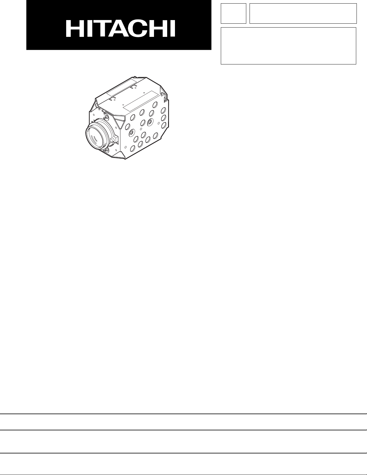
VK-S274R/S274ER
SERVICE MANUAL
VK-K274R/K274ER
SPECIFICATIONS AND PARTS ARE SUBJECT TO CHANGE FOR IMPROVEMENT
COLOR & B/W VIDEO CAMERA
2003March
Digital Media Division,Tokai
Page 2

Table of Contents
1 Safety Precaution for Repair ............. 1-1
1-1 Cautions ................................................... 1-1
1-2 Notes When Using Service Manual .......... 1-1
1-2-1 Value units used in parts list .................. 1-1
1-2-2 Values in schematic diagrams ............... 1-1
1-2-3 Identifications of sides A/B in
circuit board diagrams ........................... 1-2
1-2-4 Table for indexing locations of parts ....... 1-2
1-3 Electrostatic Protection Measures ............ 1-3
1-3-1 Grounding for prevention of
electrostatic damage ............................. 1-3
1-3-2 Cautions when handling
optical pickup......................................... 1-3
1-4 Lead-Free Solder...................................... 1-4
1-4-1 Characteristics of lead-free solder ......... 1-4
1-4-2 Solder for servicing................................ 1-4
1-4-3 Soldering iron for servicing .................... 1-4
2 General Description ........................... 2-1
2-1 Overview .................................................. 2-1
2-1-1 Servicing method................................... 2-1
2-2 Features ................................................... 2-1
2-3 Specifications ........................................... 2-2
2-4 Comparison of Main Control ICs............... 2-4
6-1-4 Setting test equipment ........................... 6-3
6-1-5 Starting adjustment program (ZMAP) .... 6-3
6-2 List of Adjustment Items ........................... 6-5
6-2-1 List of adjustments needed after
replacing major...................................... 6-5
6-2-2 Adjustment flowchart ............................. 6-6
6-3 Data Initialize ............................................ 6-7
6-4 Electronic Volume ..................................... 6-7
6-4-1 CDS sampling pulse adjustment............ 6-8
6-5 Adjustment (Camera Adjustment)............. 6-8
6-5-1 Auto iris control adjustment ................... 6-9
6-5-2 White balance adjustment ..................... 6-9
6-5-3 Chroma gain adjustment ....................... 6-10
6-6 Auto Focus ............................................... 6-11
6-6-1 Zoom/focus tracking adjustment ............ 6-11
6-6-2 AF noise level adjustment ...................... 6-12
6-6-3 Check of zoom/focus trace .................... 6-12
6-7 Spot Noise ................................................ 6-13
6-8 Error Messages and Countermeasure ...... 6-14
7 Exploded View and Parts List............ 7-1
7-1 Exploded View .......................................... 7-1
7-2 Replacement Parts List ............................ 7-2
7-2-1 Mechanical parts list .............................. 7-2
7-2-2 Electrical parts list ................................. 7-2
3 Description of Operation ................... 3-1
3-1 Structure Schematics ............................... 3-1
3-2 Microprocessor Pin Function Tables ......... 3-2
3-2-1 Camera microprocessor
(IC1201: Camera µP)............................. 3-2
4 Troubleshooting.................................. 4-1
4-1 Trouble Diagnosis ..................................... 4-1
4-1-1 Setting to service position...................... 4-1
4-1-2 Trouble diagnosis flowchart ................... 4-2
5 Disassembly and Reassembly .......... 5-1
5-1 Order of Disassembly ............................... 5-1
5-2 Disassembly ............................................. 5-1
6 Adjustment .......................................... 6-1
6-1 Preparations for Adjustment ..................... 6-1
6-1-1 List of equipment and jigs ...................... 6-1
6-1-2 List of test equipment and charts ........... 6-1
6-1-3 Connections for adjustment ................... 6-2
Schematic, Circuit Board and Block
Diagrams .................................................... 1
1 Wiring Diagram .............................................. 1
2 Schematic Diagrams ..................................... 2
2-1 Sensor [SP] Schematic Diagram ............... 2
2-2 Process [PC] Schematic Diagram
(For Display) .............................................. 3
2-3 Process [PC] Schematic Diagram
(For Printing) A-a ....................................... 4
2-4 Process [PC] Schematic Diagram
(For Printing) A-b ....................................... 5
2-5 Switching Reg. [CSR] ................................ 6
3 Circuit Board Diagram ................................... 7
3-1 PC Circuit Board Diagram ......................... 7
3-2 SP Circuit Board Diagram.......................... 8
3-3 CSR Circuit Board Diagram ....................... 8
3-9 Identification Parts Location....................... 9
4 Block Diagrams ............................................. 10
4-1 Overall Block Diagram ............................... 10
4-2 Power Block Diagram ................................ 11
Page 3
1
Safety Precaution for Repair
1-1 Cautions
PRODUCT SAFETY NOTICE
Many electrical and mechanical parts have special safety-related characteristics. These are often not
evident from visual inspection nor can the protection afforded by them necessarily be obtained by using
replacement components rated for a higher voltage, wattage, etc. Replacement parts which have these
special safety characteristics are identified in this Service Manual. Electrical components having such
features are identified by marking with a on the schematics and the parts list in this Service Manual.
The use of a substitute replacement component which does not have the same safety characteristics as
the HITACHI recommended replacement one, shown in the parts list in this Service Manual, may create
shock, fire, or other hazards. Product safety is continuously under review and new instructions are issued
from time to time. For the latest information, always consult the current HITACHI Service Manual. A
subscription to, or additional copies for, HITACHI Service Manual may be obtained at a nominal charge
from HITACHI SALES CORPORATION.
1-2 Notes When Using Service Manual
The following shows the contents to be noted when using service manual:
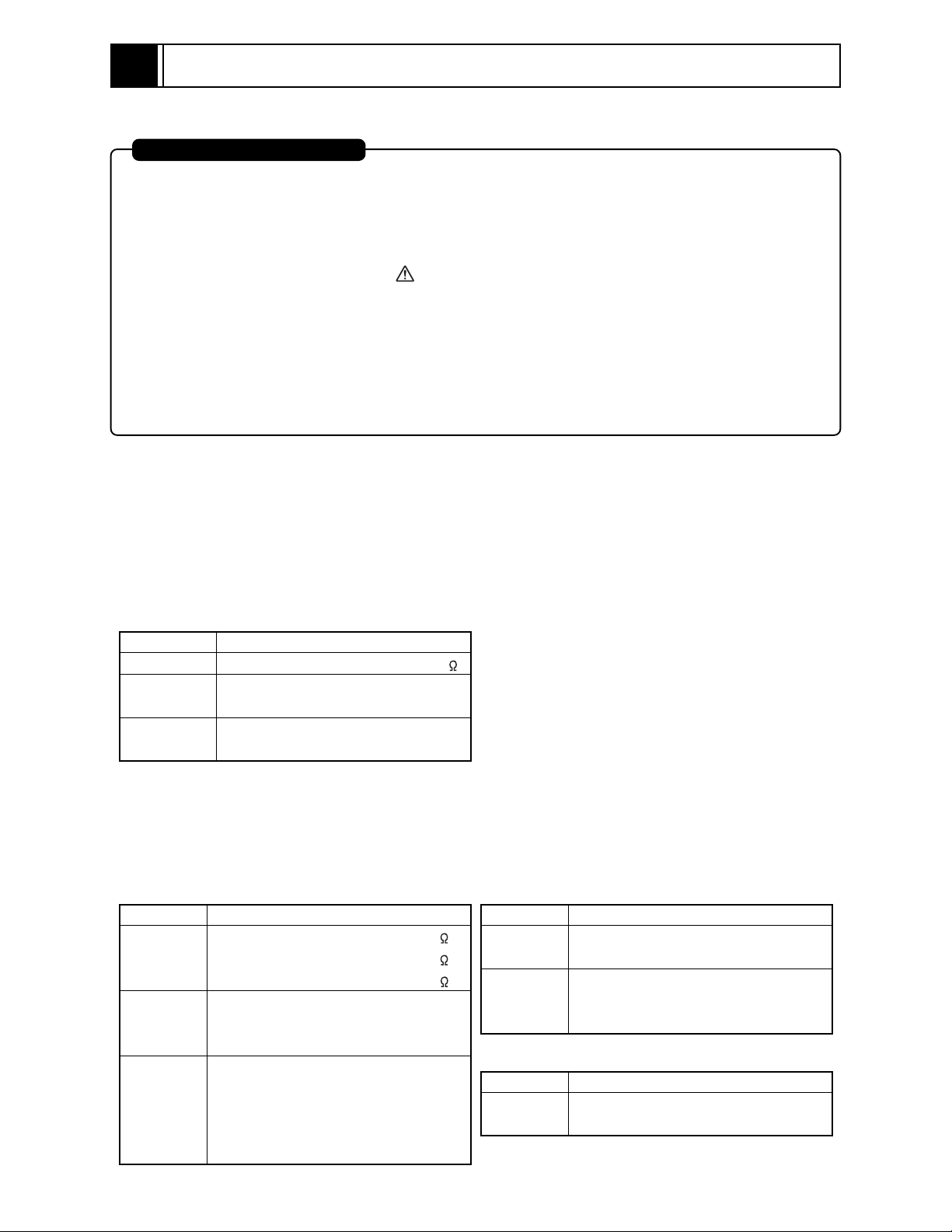
1-2-1 Value units used in parts list
Certain symbols are indicated below for value units of resistors, capacitors and coils in parts list. When you read
them note the following regular indications:
Parts
Resistor
Capacitor
Coil
Indication in list Regular indication
...........................................
KOHM
................................................
UF
................................................
PF
................................................
UH
...............................................
MH
k
µF
pF
µH
mH
1-2-2 Values in schematic diagrams
The values, dielectric strength (power capacitance) and tolerances of the resistors (excluding
variable resistors) and capacitors are indicated in the schematic diagrams using abbreviations.
[Resistors] [Capacitors]
Item
Value
Tolerance
Power
capacitance
Indication
No indication
...................................................
K
..................................................
M
No indication
(All tolerances other than ±5% are
indicated in schematic diagrams)
No indication
(1/16W for leadless resistors without
indication)
All capacitances other than the above
are indicated in schematic diagrams.
...................................
.............................
............................
±5%
1/8W
k
M
Item
Value
Dielectric
strength
[Coils]
Item
Value
1 - 1
Indication
No indication
...................................................
P
No indication
(All dielectric strengths other than 50V
are indicated in schematic diagrams)
Indication
....................................................
µ
..................................................
m
.................................
..............................
50V
µF
pF
µH
mH
Page 4
Safety Precaution for Repair > Notes When Using Service Manual
1-2-3 Identifications of sides A/B in circuit board diagrams
1) Board having a pattern on one side and parts on both sides.
Side A: Shows discrete parts, viewed from the pattern side.
Side B: Shows leadless parts, viewed from the pattern side.
2) Board having patterns on both sides and parts on both sides.
Side A: Shows parts and patterns which can be seen when the case is opened.
Side B: Shows parts and the pattern on the back of side A.
1-2-4 Table for indexing locations of parts
The table of “Identification of parts location” on circuit board diagrams shows locations of each part
as below explanations. The locations are indicated using the guide scales on the external lines of
diagrams.
1) One diagram indicated for each board
Symbol
No.
IC
IC1201
Circuit No.
Parts
Location
Type of part
2 A
Zone "A" on board diagram
Zone "2" on board diagram
2) Two diagrams indicated for each board
Symbol
No.
Parts
Location
IC
IC1201
A: Shows side A
B: Shows side B
A - 2 A
Zone "A" on board
diagram
Zone "2" on board
diagram
1 - 2
Page 5
Safety Precaution for Repair > Electrostatic Protection Measures
1-3 Electrostatic Protection Measures
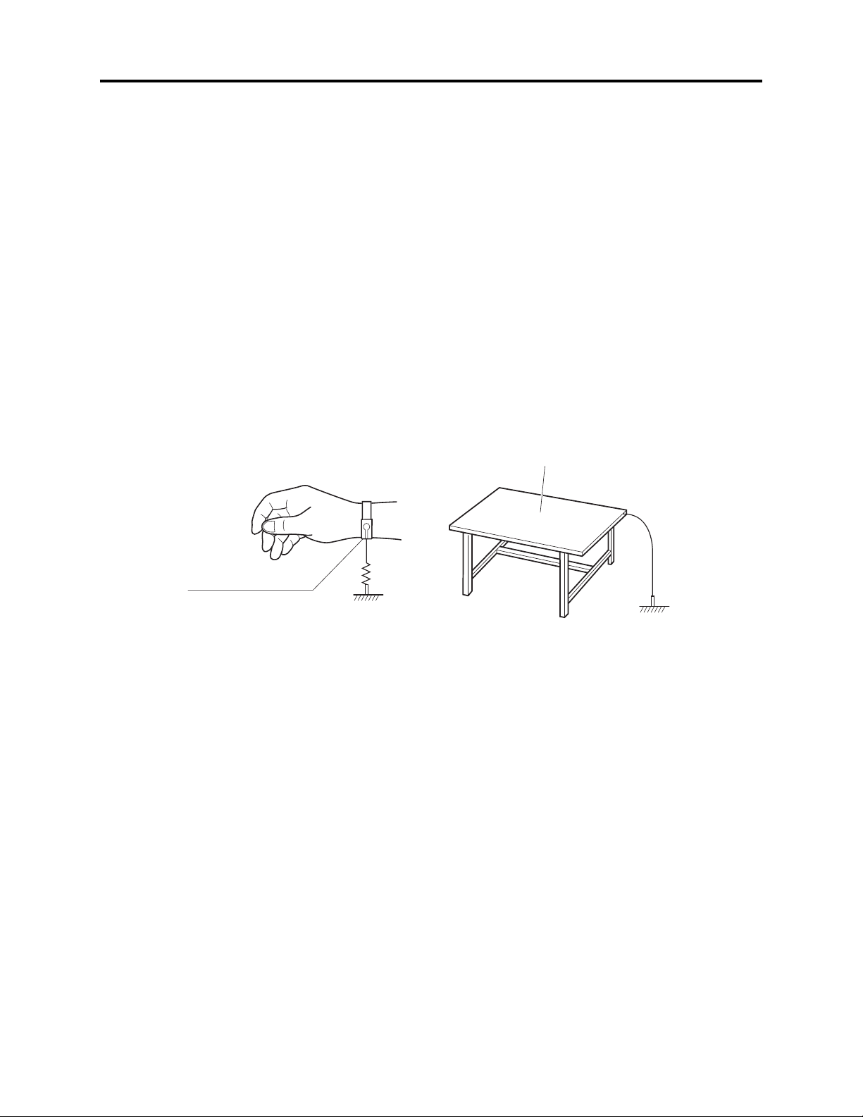
Semiconductor components, including optical pickups, may be damaged by static electricity charged
on clothes, human body, etc. Take great care when handling it to avoid electrostatic damage.
1-3-1 Grounding for prevention of electrostatic damage
Perform servicing in an environment where grounding is complete.
Grounding work bench
1) Lay out a conductive material (conductive sheet) or iron plate under the work bench on which
semiconductor components, such as optical pickups, are placed to ground the bench.
Grounding human body
1) Use an anti-static wrist strap to discharge static electricity charged on human body. Note,
however, that static electricity charged on clothes will not be discharged by anti-static wrist
strap: Be careful that your clothes do not touch the semiconductor components, such as optical
pickups.
Conductive material (conductive sheet)
or iron plate
Anti-static wrist strap
1M ohm
Ground
1-3-2 Cautions when handling optical pickup - only for DVD products
1) The optical pickup has a high precision structure: Do not subject it to any impact.
2) Do not perform disassembly further than that described in this manual.
3) Never turn the semi-variable resistors in drive unit block.
1 - 3
Page 6

Safety Precaution for Repair > Lead-Free Solder
1-4 Lead-Free Solder
To protect the global environment, lead-free solder is used in this product.
Be sure to read the following before soldering.
Caution
Be sure to wear protective goggles so that no solder smoke or scattered solder enters the eye during
servicing. Lead-free solder may scatter at high temperatures (600°C).
1-4-1 Characteristics of lead-free solder
The melting point of lead-free solder is 30-40°C higher than that of lead based solder.
Composition of alloy (wt%): Sn-3.0Ag-0.5Cu
Melting temperature: Approx. 220°C
1-4-2 Solder for servicing
It is recommended that you use lead-free solder whose characteristics are the same as that used in
this product, although it is also possible to service using lead based solder. However, if lead based
solder is used for servicing, some precautions are necessary. (Neglecting these could decrease
strength, causing malfunctions.)
Cautions when using lead based solder:
When replacing components, remove the lead-free solder previously used for soldered points as
far as possible.
For additional soldering, melt lead-free solder completely and mix well with lead based solder.
Never perform repair using the bare soldering iron tip without adding solder.
1-4-3 Soldering iron for servicing
It is recommended that you use a soldering iron with thermal control function, with which the
temperature at its tip can be set.
Lead-free solder melts at a temperature 30-40°C higher than lead based solder. Therefore,
workability will be reduced unless you use a soldering iron whose temperature is high, whose
temperature at tip does not change greatly (heat capacity is large), and that can be set to match the
work points.
Recommended soldering iron:
With thermal control function (temperature setting range: 320-450°C)
Recommended tip temperatures for different work points:
Work point
Circuit board with surface-mounted (chip) parts
Circuit board without surface-mounted (chip) parts
Chassis, metal shield
Recommended tip temperature
320°C ± 30°C
380°C ± 30°C
420°C ± 30°C
1 - 4
Page 7
2
General Description
2-1 Overview
VK-S274R/S274ER is a color chassis video camera; VK-K274R/K274ER is a Black-and-white chassis
video camera: All these models incorporate an optical 22-power compact zoom lens.
Models VK-S274R/S274ER/K274R/K274ER are successor cameras to VK-S274/S274E/K274/K274E.
The signal process circuit is equipped with a digital signal processor (D.S.P.5) that is the same as
that of VK-S274/S274E/K274/K274E.
The external appearance is identical to VK-S274/S274E/K274/K274E.
2-1-1 Servicing method
Table 2-1-1 shows the method for servicing each circuit board.
Refer to "4 Troubleshooting" for the method of judging defects in each circuit board.
Information:
These servicing methods are subject to change without notice for the purpose of facilitating service
procedures.
PC CIRCUIT
Table 2-1-1 Circuit Board Servicing Method
Circuit board
CSR circuit board
PC circuit board
SP circuit board
Servicing method
Component replacement.
PC CIRCUIT
BOARD
BOARD
SP
CIRCUIT
BOARD
CSR CIRCUIT
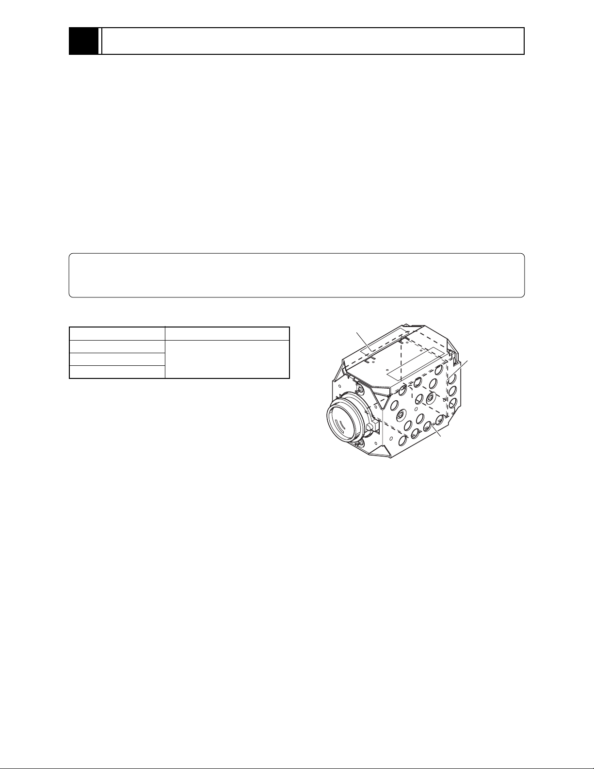
BOARD
Fig. 2-1-1 Locations of Circuit Boards
2-2 Features
Built-in Optical Power Zoom Lens
A highly reliable optical 22-power zoom lens is mounted, and it is equipped with auto-focus and auto
iris functions.
12-Power Digital Zoom Function
The 12-power digital zoom, combined with the 22-power optical zoom, makes possible up to 264power zooming.
Remote Control via RS-232C
Focus, iris and zoom can be remotely operated via RS-232C.
External Synchronization with AC-Line Pulse Signal
This chassis camera is compatible with external sync using AC-line pulse signal, as well as with
internal sync.
2 - 1
Page 8
General Description > Specifications
2-3 Specifications
The specifications in shaded columns are different from those of previous models.
Design and specifications are subject to change without notice.
Item
Signal Format
Scanning System
Scanning
Frequency
Image Sensor
Lens
Signal Processing
Sync. System
Camera
Functions
(Control
through
RS-232C)
Horizontal
Vertical
Total Pixels
Effective Pixels
Angle of View
Min. Distance
Optical Zoom
Digital Zoom
Video Focus
White Balance
Shutter Speed
Auto (Pro-AE)
Auto (Pro-AE+)
Manual
*: Default settings
VK-S274R/S274ER
VK-K274R/K274ER
VK-S274R: NTSC
VK-K274R: EIA B/W
VK-S274ER: PAL
VK-K274ER: CCIR B/W
2:1 Interlacing
VK-S274R/K274R: 15.734 kHz
VK-S274ER/K274ER: 15.625 kHz
VK-S274R/K274R: 59.94 Hz
VK-S274ER/K274ER: 50 Hz
1/4-inch CCD
VK-S274R/K274R:
811 (H) × 508 (V), 410k
VK-S274ER/K274ER:
795 (H) × 596 (V), 470k
VK-S274R/K274R:
768 (H) × 494 (V), 380k
VK-S274ER/K274ER:
752 (H) × 582 (V), 440k
F1.6 f = 4 - 88 mm, High Durability
×22 Zoom Lens, Video Auto Focus
Horizontal 47°(Wide), 2.2°(Tele)
1.0m (Tele), 0.01m (Wide)
Digital Signal Processor (D.S.P. 5)
Internal/External
TELE-WIDE (Zoom speed: 3.9s*/6.3s)
Off*/On (Up to 12×)
Auto*/Manual (NEAR-FAR/Fix)
Auto*/Manual (Red/Blue Gain: UPDOWN/Fix)
VK-S274R/K274R: 1/60 - 1/4000s
VK-S274ER/K274ER: 1/50 - 1/4000s
VK-S274R/K274R:
1/2 - 1/4* - 1/4000s
VK-S274ER/K274ER:
1/1.5 - 1/3* - 1/4000s
VK-S274R/K274R:
Shutter (1/2 - 1/4000s)/
Exposure (F1.6 - F34)/
AGC priority (0 - 27dB)
VK-S274ER/K274ER:
Shutter (1/1.5 - 1/4000s)/
Exposure (F1.6 - F34)/
AGC priority (0 - 27dB)
VK-S274: NTSC
VK-K274: EIA B/W
VK-S274E: PAL
VK-K274E: CCIR B/W
2:1 Interlacing
VK-S274/K274: 15.734 kHz
VK-S274E/K274E: 15.625 kHz
VK-S274/K274: 59.94 Hz
VK-S274E/K274E: 50 Hz
1/4-inch CCD
VK-S274/K274:
VK-S274E/K274E:
VK-S274/K274:
VK-S274E/K274E:
F1.6 f = 4 - 88 mm, High Durability
×22 Zoom Lens, Video Auto Focus
Horizontal 47°(Wide), 2.2°(Tele)
1.0m (Tele), 0.01m (Wide)
Digital Signal Processor (D.S.P. 5)
Internal/External
TELE-WIDE (Zoom speed: 3.9s*/6.3s)
Off*/On (Up to 12×)
Auto*/Manual (NEAR-FAR/Fix)
Auto*/Manual (Red/Blue Gain: UPDOWN/Fix)
VK-S274/K274: 1/60 - 1/4000s
VK-S274E/K274E: 1/50 - 1/4000s
VK-S274/K274:
VK-S274E/K274E:
VK-S274/K274:
VK-S274E/K274E:
VK-S274/S274E
VK-K274/K274E
811 (H) × 508 (V), 410k
795 (H) × 596 (V), 470k
768 (H) × 494 (V), 380k
752 (H) × 582 (V), 440k
1/2 - 1/4* - 1/4000s
1/1.5 - 1/3* - 1/4000s
Shutter (1/2 - 1/4000s)/
Exposure (F1.6 - F34)/
AGC priority (0 - 27dB)
Shutter (1/1.5 - 1/4000s)/
Exposure (F1.6 - F34)/
AGC priority (0 - 27dB)
2 - 2
Page 9
General Description > Specifications
Item VK-S274R/S274ER
Camera
Functions
(Control
through
RS-232C)
Sensitivity
Horizontal Resolution
Luminance S/N
Video output
Supplied Voltage
Power Requirement
Operating Temperature
Operating Humidity
Dimensions
Weight
Mirror
Mosaic
Iris Control
Privacy Zone
Masking
Freeze
Extrenal Sync.
Communication
Speed of RS-232C
Position Preset
*: Default settings
VK-K274R/K274ER
Off*/On
Off*/On
*
Auto
Off/On* (2 zone 2-D/8 zone 3-D)
Off*/On
Off*/On
Selective (4.8k*/9.6k/19.2k/38.4/57.6k
bps)
No-Trace preset/Trace preset
(Memory: max. 64 position)
VK-S274R/S274ER:
1.0 lx (Pro-AE: 1/60s or 1/50s,
F1.6, 27dB)
0.06 lx (Pro-AE+: 1/4s)
VK-K274R/K274ER:
0.1 lx (Pro-AE: 1/60s or 1/50s,
F1.6, 27dB)
0.01 lx (Pro-AE+: 1/4s)
VK-S274R: More than 470 TV lines
VK-S274ER: More than 460 TV lines
VK-K274R/K274ER:
More than 500 TV lines
More than 50dB
VK-S274R/S274ER:
Composite: 1.0 ± 0.2Vp-p
VK-K274R/K274ER:
Y (Luminance): 1.0 ± 0.2Vp-p
9 V - 12 V DC ± 0.5 V
3.65 W (When suppling 9 V DC)
0 - 60° (Recommended: 0 - 40°)
10 - 90%
50 (W) × 60 (H) × 89.5 (D) mm
Approx. 222g
VK-S274/S274E
VK-K274/K274E
Off*/On
Off*/On
*
Auto
Off/On* (2 zone)
Off*/On
Off*/On
Fixed (4.8k bps)
----------
VK-S274/S274E:
1.0 lx (Pro-AE: 1/60s or 1/50s,
F1.6, 27dB)
0.1 lx (Pro-AE+: 1/4s)
VK-K274/K274E:
0.1 lx (Pro-AE: 1/60s or 1/50s,
F1.6, 27dB)
0.01 lx (Pro-AE+: 1/4s)
VK-S274: More than 470 TV lines
VK-S274E: More than 460 TV lines
VK-K274/K274E:
More than 500 TV lines
More than 50dB
VK-S274/S274E:
Composite: 1.0 ± 0.2Vp-p
VK-K274/K274E:
Y (Luminance): 1.0 ± 0.2Vp-p
9 V DC ± 0.5 V
3.3 W (When suppling 9 V DC)
0 - 60° (Recommended: 0 - 40°)
10 - 90%
50 (W) × 60 (H) × 89.5 (D) mm
Approx. 225g
2 - 3
Page 10

General Description > Comparison of Main Control ICs
2-4 Comparison of Main Control ICs
The comparison of main control ICs in shaded columns are different from those of previous models
Item
Image Sensor
Sensor Drive
CDS/AGC & A/D Conv.
Camera DSP
DRAM
Inv.
Clock Gen.
Camera µP
EEPROM
Reset Pulse Gen.
Zoom Motor Drive
Focus Motor Drive
F.DET./Iris Drive
PWM
7.2V Reg.
Y/C Mix & Video Amp
Level Shift
VCO/Phase Compa.
FV Pulse Gen.
VK-S274R/S274ER
VK-K274R/K274ER
VK-S274R: ICX278AK-L (IC1001)
VK-S274ER: ICX279AK-L (IC1001)
VK-K274R: ICX278AL-7 (IC1001)
VK-K274ER: ICX279AL-7 (IC1001)
µPD16510GR (IC1002)
HD49323AF (IC1101)
HG73C053FE (IC1121)
IC41LV16100S-50G (IC1122)
TC7SU04FU (IC1173)
TC7SHU04FUL (IC1174)
HD6432238RN41FA (IC1201)
BR9016RFV (IC1202)
BR9016RFV (IC1203)
NC7SZ14P5 (IC1204)
NC7SZ14P5 (IC1205)
SN74AHC1G08HDCK (IC1206)
RN5VD27AA (IC1251)
TB6512AF (IC1301)
TB6512AF (IC1302)
µPC5023GS-147-GJG (IC1351)
TL1464IPT (IC1501)
PQ20WZ51 (IC1502)
BA7665FS (IC1601)
SN74AHCT125PW (IC1602)
74VHC4046MTCX (IC1603)
SN74AHC1G08HDCK (IC1604)
VK-S274/S274E
VK-K274/K274E
VK-S274: ICX278AK-L (IC1001)
VK-S274E: ICX279AK-L (IC1001)
VK-K274: ICX278AL-7 (IC1001)
VK-K274E: ICX279AL-7 (IC1001)
µPD16510GR (IC1002)
HD49323AF (IC1101)
HG73C053FE (IC1121)
MSM51V18165F (IC1122)
TC7SU04FU (IC1173)
TC7SHU04FUL (IC1174)
HD6432238RN30FA (IC1201)
X25097V1-2.7 (IC1202)
TC7SH14FU (IC1204)
TC7SH14FU (IC1205)
TC7S08FU (IC1206)
RN5VD27AA (IC1203)
MPC17AT85VM (IC1301)
MPC17AT85VM (IC1302)
µPD5023GS-147-GJG (IC1351)
TL1464IPT (IC1501)
---------BA7664FV (IC1601)
HD74HCT125T (IC1602)
74VHC4046MTCX (IC1603)
IDC-7S08 (IC1604)
2 - 4
Page 11
3
Description of Operation
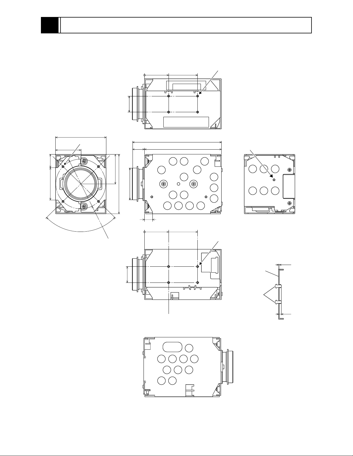
3-1 Structure Schematics
0
16Ø32.2mm
24mm
53mm
4 - M2 SCREWS for
TRIPOD PLATE
(These screws are limit of height
keep as being less than 2 mm for "A")
13.5mm33mm
50mm
4 - M2 SCREWS
25mm
90˚
Ø50m
m
30mm
60mm
12.5mm
16mm
89.5mm
77mm
8
0
24mm
4 - M2 SCREWS for
53mm
TRIPOD PLATE
(These screws are limit of height
keep as being less than 2 mm for "A")
M2 SCREW
0.8mm
CHASSIS
M2 SCREW
Fig. 3-1-1 Structure Schematics
3 - 1
A
Page 12
Description of Operation > Microprocessor Pin Function Table
3-2 Microprocessor Pin Function Table
3-2-1 Camera microprocessor (IC1201: Camera µP)
Pin
No.
1
2
3
4
5
6
7
8
9
10
11
12
13
14
15
16
17
18
19
20
21
22
23
24
25
26
27
28
29
30
31
32
33
34
35
36
37
I/O
O
O
O
O
-----
----O
O
O
O
O
-----
I
----O
O
O
I
O
-----
-----
I
-----
I
----O
O
O
----O
-----
----O
O
O
O
O
Active
Level
(Pulse)
(Pulse)
(Pulse)
Hi
(Pulse)
(Pulse)
(Pulse)
(Pulse)
(Pulse)
-----
Hi/Lo
-----
Hi/Lo
(Pulse)
Hi
(Pulse)
-----
-----
-----
0V-3V
----
0V-3V
----Hi
Hi
(Pulse)
-----
(Pulse)
-----
-----
(Pulse)
Hi/Lo
(Pulse)
(Pulse)
-----
Abbreviation
LD-DSP
CS-DAC
CS-VAP
GYRO-RST
CEON
CHARGE
RDOEB
ZDOEB
RDCK
ZDCK
IRDCK
VCC1
LINE-SW
GND1
IRDCW
IROREB
IR-RESET
IR-SENS
IR-LED
NC1
TST-PIN1
H-VAP
TST-PIN0
V-VAP
CHECK8
ZD-RESET
RD-RESET
IRIS-PWM
LD-JIG
ZOOM-LED
TXD2
RXD2
FCUS-LED
ZDCW
RDCW
ZD-PWMA
RD-PWMA
Function
Activates data communication with IC1121 (CAMERA DSP).
Not used. Open.
Activates focus drive data communications with IC1302 (FOCUS
MOTOR DRIVE).
Activates zoom drive data communications with IC1301 (ZOOM
MOTOR DRIVE).
Outputs focus motor drive signal to IC1302 (FOCUS MOTOR DRIVE).
Outputs zoom motor drive signal to IC1301 (ZOOM MOTOR DRIVE).
Not used. Open.
3V power input.
External sync detection input. When "Hi" is input, the unit will be
driven in the external sync mode; when "Lo" is input, it will be driven
in the internal sync mode.
Ground.
Not used. Open.
Not used. Open.
Resets IC1301 (ZOOM MOTOR DRIVE).
Resets IC1302 (FOCUS MOTOR DRIVE).
Iris motor drive output .
Not used. Open.
Output pulses to drive the ZOOM LED in the lens block via Q1201
(LED DRIVE).
Not used.
Output pulses to drive the FOCUS LED in the lens block via Q1201
(LED DRIVE).
Issues a command which determines with IC1301 (ZOOM MOTOR
DRIVE).
Issues a command which determines with IC1302 (FOCUS MOTOR
DRIVE).
Not used. Open.
3 - 2
Page 13

Description of Operation > Microprocessor Pin Function Table
Pin
No.
38
39
40
41
42
43
44
45
46
47
48
49
50
51
52
53
54
55
56
57
58
59
60
61
62
63
64
65
66
67
68
69
70
71
72
73
74
75
76
77
78
I/O
I
I
----I
-----
O
O
I
I
I
I
I
I
I
I
-----
-----
-----
-----
-----
----I
-----
-----
----I
-----
O
I
I
-----
O
-----
----I
-----
----I
O
I
I
Active
Level
(Pulse)
(Pulse)
-----
(Pulse)
----0V-3V
0V-3V
0V-5V
0V-3V
0V-3V
0V-3V
0V-3V
0V-3V
0V-3V
0V-3V
-----
-----
-----
-----
-----
-----
Lo
-----
-----
-----
(Pulse)
------
(Pulse)
Lo
Hi
-----
Hi
-----
-----
(Pulse)
-----
-----
(Pulse)
(Pulse)
(Pulse)
(Pulse)
Abbreviation Function
FV
FCUS-SEN
NC2
ZOOM-SEN
GND2
HAL-ADJ1
HAL-ADJ0
5V_DET
ZOOM-SW
FOCUS-SW
+B_DET
TEMP-ADJ
V-GYRO
H-GYRO
FDET
AVCC1
AVCC2
VCC2
VCC3
NC4
NC5
SYS-REST
VCC4
STBY
VCC5
XTAL
GND3
EXTAL
FWE
MD2
NC6
HALL-G
NC7
NC8
HD
SHUT-CTL
STROBE
FP
SD[232C]
RD[232C]
EP3
Receives the vertical sync pulses that detect the iris detection area,
from IC1121 (CAMERA DSP).
Focus motor position detection input.
Not used. Open.
Zoom motor position detection input.
Ground.
Controls the offset voltage of IC1351 (F.DET/IRIS DRIVE).
Drives bias generator in IC1351 (F.DET/IRIS DRIVE) via Q1351
(BIAS DRIVE) to control the bias voltage of the Hall devices.
DC5V detection input. Monitors the 5V line voltage.
Not used.
Power voltage (+B) detection input. Monitors the +B line voltage.
Temperature change detection input. Detects variations in the
forward voltage at the connected diode to correct the back-focus.
Not used. Connect to ground.
F-value detection input. Receives the F.DET voltage detected by
IC1351 (F.DET/IRIS DRIVE) and compares this with the reference
voltage input via pin 53 to detect the F-value.
Reference 3V power input.
A/D reference voltage input (connected to 3V power supply).
3V power input.
Not used. Open.
Not used. Connect to ground.
Reset signal input from IC1206 (RESET PULSE GEN.).
3V power input.
Not used. Connect to 3V power supply.
3V power input.
Not used. Open.
Grounded.
Inputs controk pulses from IC1211 (CAMERA DSP).
Not used.
Not used. Open.
Controls the amplification (gain of Hall device) of IC1351 (F.DET/IRIS
DRIVE).
Not used. Open.
Inputs horizontal sync from IC1121 (CAMERA DSP).
Not used. Open.
Inputs field discrimination pulse from IC1121 (CAMERA DSP).
Used for initial settings and adjustment. For data communications
with personal computer.
Receives pulses which discriminate the iris detection area.
3 - 3
Page 14
Description of Operation > Microprocessor Pin Function Table
Pin
No.
79
80
81
82
83
84
85
86
87
88
89
90
91
92
93
94
95
96
97
98
99
100
I/O
-----
-----
-----
----O
I
O
-----
-----
I
-----
I
-----
-----
-----
----O
O
O
O
O
O
Active
Level
-----
-----
-----
----(Pulse)
(Pulse)
(Pulse)
-----
----(Pulse)
-----
Hi/Lo
-----
-----
-----
-----
Hi/Lo
(Pulse)
(Pulse)
(Pulse)
(Pulse)
(Pulse)
Abbreviation Function
NC9
NC10
NC11
NC12
SDO
SDI
SCLK
DC-LIGHT
NC13[1]
4800SET
LIGHT-SW
COLOR/BW
NC13[2]
F-DIAL1
F-DIAL2
LIGHT-0
STBY_5V
CLK-CDS
SDO-CDS
CS-CDS
CS-EE[1]
CS-EE[2]
Not used. Open.
For data communications with IC1121 (CAMERA DSP), IC1202
(EEPROM), IC1203 (EEPROM).
Not used. Open.
Not used.
Not used. Open.
Color model and B/W model select input. (Hi: Color model/Lo: B/W
model)
Not used. Open.
5V regulator control output. (Hi: On/Lo:Off)
Transfer data to IC1101 (CDS/AGC & A/D CONV. ).
Activates data communications with IC1101 (CDS/AGC & A/D
CONV. ).
Activates data communications with IC1202 (EEPROM).
Activates data communications with IC1203 (EEPROM).
3 - 4
Page 15
4
Troubleshooting
4-1 Trouble Diagnosis
4-1-1 Setting to service position
Remove chassis R and chassis L, referring to “5. Disassembly and Reassembly”, and connect the
camera as shown in Fig. 4-1-1.
Note:
To prevent short-circuit, always perform trouble diagnosis of camera on insulated mat.
PC CIRCUIT
BOARD
SP CIRCUIT
BOARD
CSR CIRCUIT
BOARD
PG1601
DSP INTERFACE CONNECT JIG
(Parts No. 7069179)
1
RD WHT
2
SD BRW
3
GND BRW
4
+B BRW
5
GND BRW
6
VIDEO BRW
7
GND(VIDEO) BRW
8
EX. FV BRW
9
GND BRW
DC POWER
SUPPLY
(9V/3A)
+
GND
Fig. 4-1-1 Connections for Trouble Diagnosis
9PIN FLAT CABLE
(ACCESSORY)
9
1
2345
1
6
78
COLOR MONITOR
9
VIDEO IN
4 - 1
Page 16
Troubleshooting > Trouble Diagnosis
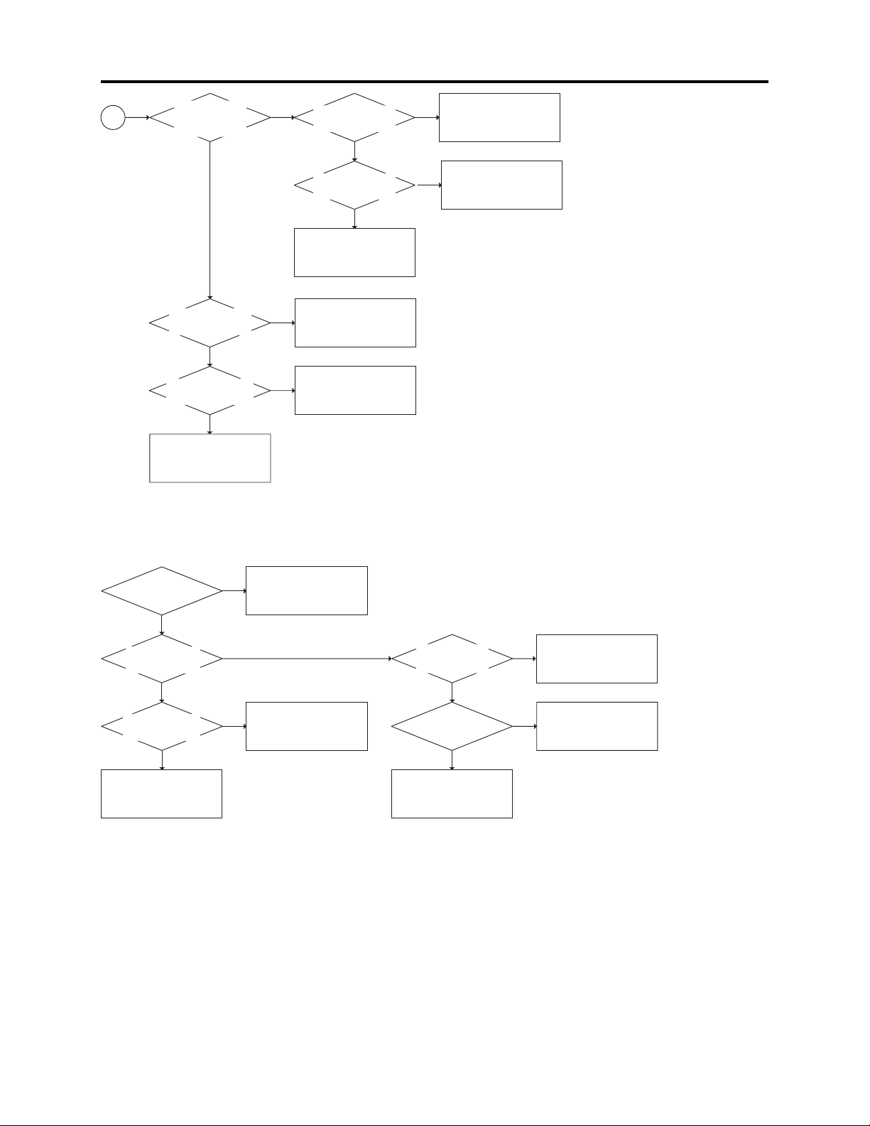
4-1-2 Trouble diagnosis flowchart
(1) No video (luminance) signal
The test lands and components of circuit no. 1000-1099 are
on the SP circuit board.
The test lands and components of circuit no. 1100-1499 are
on the PC circuit board.
The test lands and components of circuit no. 1500 and higher
are on the CSR circuit board.
OK
NG
Refer to "(3) No power"TL1539 : 5V
TL1540 : 3V
OK
TL1532 : 2V
OK
TL1533 : 15V
OK
TL1534 : -7.5V
OK
TL1522 : 7.2V
OK
TL1529 :
Luminance signal
OK
IC1601 faulty
NG
Refer to "(3) No power"
NG
Refer to "(3) No power"
NG
Refer to "(3) No power"
NG
Refer to "(3) No power"
NG
Refer to "(3) No power"
NG
CCD output signal
CCD output signal
TL1013 :
OK
IC1101-27 :
OK
NG
1
C1101 faulty or connect
NG
the connections of circuit
boards.
IC1101-43, 44, 45 :
Pulses
OK
IC1101-16, 17,
18, 19 : Pulses
OK
IC1101-2 to 11:
Pulses
OK
IC1121-66:
Luminance signal
OK
Q1152 faulty.
NG
NG
NG
NG
IC1201 faulty.
IC1121 faulty.
IC1101 faulty.
TL1154: 3V
IC1121 faulty.
4 - 2
OK
NG
Q1151 or D1151 faulty.
Page 17
Troubleshooting > Trouble Diagnosis
1
TL1082, 1083,
1085, 1086 :
Pulses
OK
TL1236, 1238,
1240 : Pulses
OK
IC1001-7 :
CCD output signal
OK
Q1001 faulty.
NG
NG
NG
TL1016, 1017,
1019 : Pulses
OK
TL1018, 1020,
1024 : Pulses
OK
IC1002 faulty.
IC1121 faulty.
IC1001 faulty.
IC1121 faulty or connect
NG
the connections of circuit
boards..
IC1121 faulty or connect
NG
the connections of circuit
boards..
(2) No chroma signal [For VK-S274R/S274ER]
The test lands and components of circuit no. 1000-1099 are
Luminance
signal
TL1530 :
Chroma signal
IC1601-7 :
Chroma signal
IC1601 faulty.
OK
OK
OK
NG
Refer to "(1) No video
(luminance) signal"
NG
NG
Q1605 faulty.
on the SP circuit board.
The test lands and components of circuit no. 1100-1499 are
on the PC circuit board.
The test lands and components of circuit no. 1500 and higher
are on the CSR circuit board.
Chroma signal
IC1121 faulty.
IC1121-65 :
NG
TL1154 : 3V
OK
OK
Q1153 faulty.
NG
Q1151 or D1151 faulty.
4 - 3
Page 18
Troubleshooting > Trouble Diagnosis
(3) No power
Check fuse
(F1501)
OK
TL1609 : 9V (+B)
OK
TL1535 : 9V (+B)
OK
TL1539 : 5V
OK
TL1540 : 3V
NG
NG
NG
NG
NG
Fuse replacement
D1601 faulty
CP1601 faulty
IC1501-44 : 8V
OK
Q1501 faulty
IC1501-35 : 8V
The test lands and components of circuit no. 1000-1099 are
on the SP circuit board.
The test lands and components of circuit no. 1100-1499 are
on the PC circuit board.
The test lands and components of circuit no. 1500 and higher
are on the CSR circuit board.
NG
IC1501 faulty
NG
IC1501 faulty
OK
TL1532 : 2V
OK
TL1533 : 15V
OK
TL1534 : -7.5V
NG
OK
Q1502 faulty
NG
NG NG
OK
IC1501-2 : 8V
OK
Q1503 faulty
TL1534 : -7.5V
OK
D1501 faulty
TL1522 : 7.2V
OK
NG
NG
IC1501 faulty
Q1504 faulty
IC1502 faulty
OK
NG
IC1501 faulty IC1501-41 : 8V
D1503 faulty
Correct the connections
of circuit boards
4 - 4
Page 19

Troubleshooting > Trouble Diagnosis
(4) No zoom and focus operation
TL1301:7.2V
OK
NG
L1301 faulty
The test lands and components of circuit no. 1000-1099 are
on the SP circuit board.
The test lands and components of circuit no. 1100-1499 are
on the PC circuit board.
The test lands and components of circuit no. 1500 and higher
are on the CSR circuit board.
When power
turned on:
TL1336:Pulse
OK
TL1331 to 1334:
Pulses
NG
IC1301-2,4,
24:3V
OK
IC1301-10,
15:7.2V
OK
TL1311:Pulse
OK
IC1301-23:Pulse
OK
IC1301-20:Pulse
NG
OK
NG
NG
NG
NG
NG
Lens unit faulty.
Check the 3V line
Check the 7.2V (VM)
line
IC1201 faulty
IC1201 faulty.
IC1201 faulty.
Check the
connections of the
lens flat cable.
OK
TL1346:3V
OK
TL1335:Pulse
OK
Lens unit faulty
NG
NG
NG
Correct the
connections
of the cable.
Check the 3V line
IC1201 faulty.
R1215 faulty.
Q1201 faulty.
OK
IC1301-5:Pulse
OK
When power
turned on:
TL1345:Pulse
OK
TL1347 to 1350:
Pulses
NG
IC1302-2,4,24:3V
OK
2
NG
NG
OK
NG
IC1201 faulty.
Lens unit faulty.
Check the 3V line
Check the
connections of the
lens flat cable.
OK
TL1346:3V
OK
TL1344:Pulse
OK
Lens unit faulty.
NG
NG
NG
Correct the
connections
of the flat cable.
Check the 3V line
IC1201 faulty.
R1214 faulty.
Q1201 faulty.
4 - 5
Page 20

Troubleshooting > Trouble Diagnosis
2
NG
NG
IC1302-10,15:7.2V
OK
Check the 7.2V (VM)
line.
TL1312:Pulse
OK
IC1302-23:Pulse
OK
IC1302-20:Pulse
OK
IC1302-5:Pulse
OK
IC1302 faulty.
NG
NG
NG
NG
IC1201 faulty.
IC1201 faulty.
IC1201 faulty.
IC1201 faulty.
(5) Subject is greatly out-of-focus when zoomed
The test lands and components of circuit no. 1000-1099 are
Check the Zoom
switch unit.
OK
NG
Zoom switch faulty.
on the SP circuit board.
The test lands and components of circuit no. 1100-1499 are
on the PC circuit board.
The test lands and components of circuit no. 1500 and higher
are on the CSR circuit board.
IC1201-49:
1.2-1.6V
OK
Data Initialize and
adjust auto focus.
Does autofocus
operate normally?
OK
END
NG
D1201,C1207,R1205
faulty.
Note: For the item marked , perform all
the adjustments required when the
unit is data initialized, before
adjusting auto focus.
NG
IC1201 faulty.
4 - 6
Page 21

Troubleshooting > Trouble Diagnosis
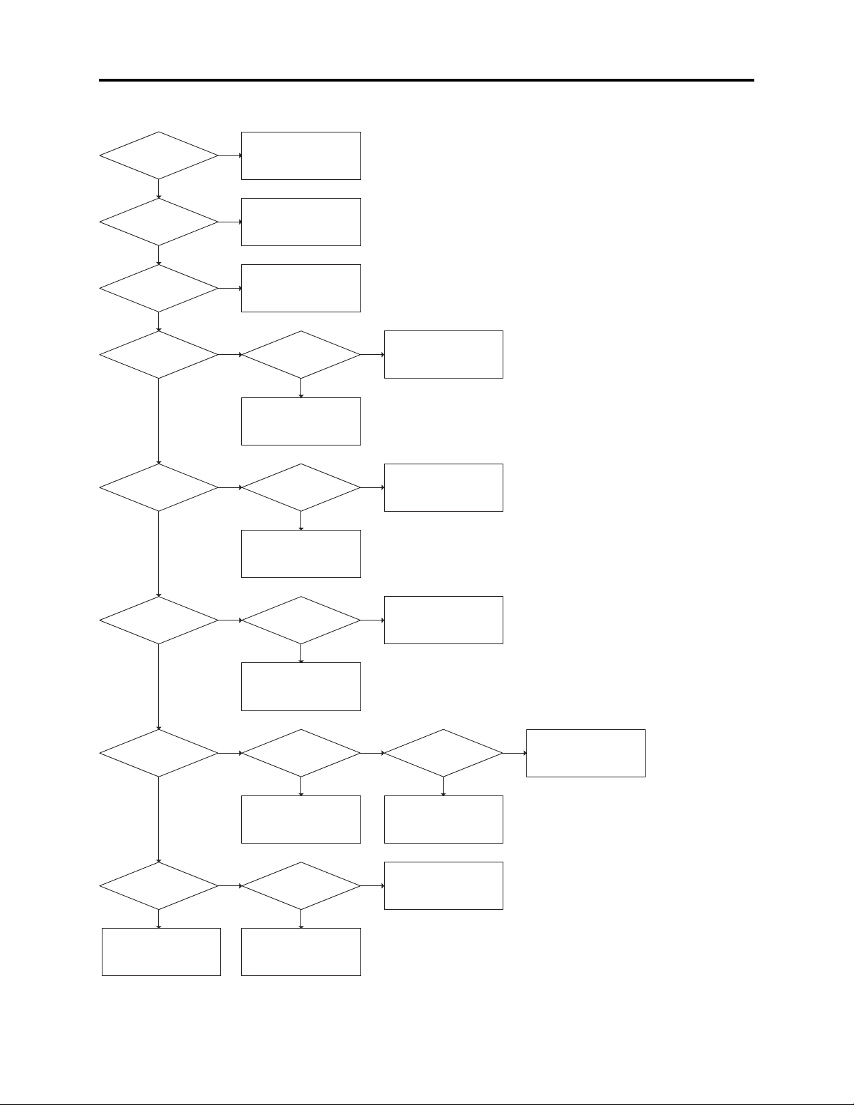
(6) No focus lens operation
Does zoom
operate
normally?
OK
NG
See "(4)No zoom and
focus operation."
The test lands and components of circuit no. 1000-1099 are
on the SP circuit board.
The test lands and components of circuit no. 1100-1499 are
on the PC circuit board.
The test lands and components of circuit no. 1500 and higher
are on the CSR circuit board.
When power
turned on:
TL1345:Pulse
OK
TL1347 to1350:
Pulses
NG
IC1302-2,4,24:3V
OK
IC1302-10,15:7.2V
OK
TL1312:Pulse
OK
IC1302-23:Pulse
OK
IC1302-20:Pulse
NG
OK
NG
NG
NG
NG
NG
Lens unit faulty.
Check the 3V line
Check the 7.2V (VM)
line
IC1201 faulty.
IC1201 faulty.
IC1201 faulty.
Check the
connections of the
lens flat cable.
OK
TL1346:3V
OK
TL1344:Pulse
OK
Lens unit faulty.
NG
NG
NG
Correct the
connections
of the flat cable.
Check the 3V line
IC1201 faulty.
R1214 faulty.
Q1201 faulty.
OK
IC1302-5:Pulse
OK
IC1302 faulty.
NG
IC1201 faulty.
4 - 7
Page 22

Troubleshooting > Trouble Diagnosis
(7) No zoom operation
Does focus operate
normally?
OK
NG
See "(4) No zoom and
focus operation."
The test lands and components of circuit no. 1000-1099 are
on the SP circuit board.
The test lands and components of circuit no. 1100-1499 are
on the PC circuit board.
The test lands and components of circuit no. 1500 and higher
are on the CSR circuit board.
Check the
zoom switch unit.
OK
When power
turned on:TL1336:
Pulse
OK
TL1331 to 1334:
Pulses
NG
IC1301-2,4,24:3V
OK
IC1301-10,
15:7.2V
OK
TL1311:Pulse
OK
IC1301-23:
Pulse
OK
NG
Zoom switch faulty.
NG
OK
NG
NG
NG
NG
Lens unit faulty.
Check the 3V line
Check the 7.2V (VM)
line
IC1201 faulty.
IC1201 faulty.
Check the
connections of the
lens flat cable.
OK
TL1346:3V
OK
TL1335:Pulse
OK
Lens unit faulty.
NG
NG
NG
Correct the
connections
of the flat cable.
Check the 3V line
IC1201 faulty.
R1215 faulty.
Q1201 faulty.
IC1301-20:
Pulse
OK
IC1301-5:Pulse
OK
IC1301 faulty
NG
NG
IC1201 faulty.
IC1201 faulty.
4 - 8
Page 23

Troubleshooting > Trouble Diagnosis
(8) No auto focus operation
Does zoom
operate
normally?
OK
Connect an
oscilloscope
to video output
VIDEO SIGNAL:
360mVp-p or more
OK
Set the zoom to the
wide-angle end.
Point at the objects
from the infinity to
close-up ends.
Is there a point at
which focus is obtained
between the infinity
and close-up ends?
OK
NG
See "(4) No zoom and
focus operation."
The test lands and components of circuit no. 1000-1099 are on the SP circuit board.
The test lands and components of circuit no. 1100-1499 are on the PC circuit board.
The test lands and components of circuit no. 1500 and higher are on the CSR circuit board.
NG
NG
Increase the
illumination
of the subject.
Does the video
level increase?
YES
TL1345:Pulse
OK
NO
Camera circuit faulty.
NG
connections of the
Check the
lens flat cable.
OK
NG
Correct the
connections
of the flat cable.
Data Initialize and
adjust auto focuss.
Does autofocus
operate normally?
OK
END
3
NG
Note: For the item marked , perform all
the adjustments required when the
unit is data initialized, before
adjusting auto focus.
IC1201 faulty.
TL1346:3V
OK
TL1344:Pulse
OK
Lens unit faulty.
NG
Check the 3V line
NG
IC1201 faulty.
R1214 faulty.
Q1201 faulty.
4 - 9
Page 24

Troubleshooting > Trouble Diagnosis
3
TL1347 to 1350:
Pulses
NG
IC1302-2,4,24:3V
OK
IC1302-10,15:7.2V
OK
TL1312 :Pulse
OK
IC1302-23:Pulse
OK
IC1302-20:Pulse
OK
IC1302-5:Pulse
OK
NG
NG
NG
NG
NG
NG
Lens unit faulty.
Check the 3V line
Check the 7.2V (VM)
line
IC1201 faulty.
IC1201 faulty.
IC1201 faulty.
IC1201 faulty.
OK
IC1302 faulty.
4 - 10
Page 25

5
Disassembly and Reassembly
5-1 Order of Disassembly
Refer to “Disassembly Flowchart” in Fig. 5-1-1 for the order of
removing components. When reassembling components, use the
reverse order to removal unless otherwise specified.
Note:
When replacing components in the VK-S274R/S274ER/K274R/
K274ER, be sure to use only those shown in "Replacement Parts
List".
Reading Disassembly Flowchart:
After locating the target component in the flowchart, remove all
components of the target in sequence, following the arrows
(routes) from the top of flowchart.
Component name
Chassis R
Chassis L
PC Circuit Board
CSR Circuit Board
SP Circuit Board
Image Sensor
Item
No.
1) and 2)
3) to 5)
6) and 7)
8) and 10)
Lens unit
11)
Fig. 5-1-1 Disassembly Flowchart
5-2 Disassembly
Information:
Numbers in figures are step numbers in disassemble procedure, and letters in brackets [ ] show
the types of screw.
Chassis L and R (Fig. 5-2-1)
1) Remove four screws [A] and remove the chassis L.
2) Remove two screws [A] and remove the chassis R.
CHASSIS R
A
B
PC
CIRCUIT
BOARD
SP
CIRCUIT
BOARD
[A] M2×3 (Black)
1 [A]
LENS
UNIT
CSR
CIRCUIT
BOARD
B
A
1 [A]
2 [A]
CHASSIS L
Fig. 5-2-1 Chassis L and R
5 - 1
Page 26

Disassembly and Reassembly > Disassembly
PC Circuit Board (Fig. 5-2-2)
3) Disconnect the flat cable from the PC circuit board.
To connect flat cables, perform the procedure in Fig. 5-2-3.
4) Remove one screw [B].
5) Remove the PC circuit board in the direction of the arrow.
CSR Circuit Board (Fig. 5-2-2)
6) Remove one screw [B].
7) Remove the CSR circuit board in the direction of the arrow.
SP Circuit Board and Image Sensor (Fig. 5-2-2)
8) Remove two screw [C] and remove image sensor assembled with SP circuit board, the crystal
filter and rubber also removed. Be careful not damage and lost them.
9) Unsolder the terminals (fourteen points) of image sensor on the SP circuit board.
10) Remove two screw [D] and remove image sensor form the SP circuit board.
Lens Unit (Fig. 5-2-2)
11) Remove three screws [C] and remove the camera chassis for the lens unit.
LENS
UNIT
PC
CIRCUIT
BOARD
RUBBER
CRYSTAL
FILTER
IMAGE
SENSOR
11 [C]
4 [B]
C
C
11 [C]
3
SP
CIRCUIT
5
BOARD
10 [D]
8 [C]
D
9
6 [B]
CAMERA
CHASSIS
D
3-1
3-2
CSR
CIRCUIT
BOARD
7
Fig. 5-2-2 PC, CSR, SP Circuit Boards, Image Sensor and Lens Unit
3-1
[B] M2×5 (Gold)
[C] M2×5 (Black)
[D] M2×3 (Gold)
FLAT
CABLE
Fig. 5-2-3 Connecting Flat Cable
5 - 2
Page 27

6
Adjustment
6-1 Preparations for Adjustment
All adjustments are performed using the adjustment program (ZMAP: Zoom camera Manual
Adjustment Program) and personal computer (PC). If error message appears during adjustment,
refer to "6-8 Error Messages and Countermeasure".
6-1-1 List of equipment and jigs
New
Adjustment Floppy
Disk (Adjustment
Program)
Personal Computer (PC)
[Goods on the Market]
*1
DSP Interface Connect
Jig No. 7069179
RS-232C Cable (9 or 25
pins) Straight Type
[Goods on the Market]
DSP-R Jig
No.7099448
*1: The adjustment floppy disk is not for sale: It will
6-1-2 List of test equipment and charts
1) Gray scale chart
2) Color bar chart
3) Backfocus chart
4) Oscilloscope
5) Vectorscope
6) Digital voltmeter (DVM)
7) 3100K light box
8) Color Monitor
9) DC power supply for the video camera
10) DC power supply for the DSP-R jig
C12 Light Balancing
Filter No.7099369
be supplied only when service maintenance
contract is concluded.
Gray Scale Chart
Color Bar Chart
Information:
It is recommended that you use a vectorscope
when performing the chroma gain adjustment.
You can use an oscilloscope instead:
Note, however, that the adjustment accuracy
will be lower.
Backfocus Chart
6 - 1
Page 28

Adjustment > Preparations for Adjustment
6-1-3 Connections for adjustment
Connect the video camera to the test equipment and jigs as shown in Fig. 6-1-1
LIGHT
BOX
DC POWER
SUPPLY
(9V/3A)
+
GND
DC POWER
SUPPLY
(5V/1A)
+
GND
VIDEO CAMERA
PG1601
DSP INTERFACE CONNECT JIG
1
RD WHT
2
SD BRW
3
GND BRW
4
+B BRW
5
GND BRW
6
VIDEO BRW
7
GND(VIDEO) BRW
8
EX. FV BRW
9
GND BRW
YEL
RED
9PIN FLAT CABLE
(ACCESSORY)
9
1
2345
1
6
78
WHT
BLK
VECTORSCOPE
To
INPUT
To
OUTPUT
OSCILLOSCOPE
CH1
CH2
9
When using an
osilloscope only
PERSONAL
COMPUTER
To VIDEO IN
TERMINAL
COLOR
MONITOR
BLK
DSP-R JIG
RS-231C
CABLE
Fig. 6-1-1 Connections for Adjustment
Note:
1) The adjustment program will not operate normally unless the video camera, PC and DSP-R jigs
are all turned on.
2) Take care with the following when pointing the video camera at a chart (light box):
a) Focus the chart correctly.
b) Set the chart (light box) 30-50 cm away from the lens surface, and avoid any effects from
surrounding light (except for a case where some designation is given).
3) Be sure to connect the video output of video camera to a color video monitor (terminate the video
output with 75 ohm):
If the video output is not connected to the monitor (and if it is not terminated with 75 ohm), the
output video signal level cannot be measured correctly.
4) Use light box that does not flicker and whose color temperature is controlled, for adjustment. If
an inappropriate light box is used, precise adjustment will not be possible, and the adjustment
program will not operate normally.
6 - 2
Page 29

Adjustment > Preparations for Adjustment
6-1-4 Setting test equipment
(1) Oscilloscope
The names of switches, knobs, modes, etc. of oscilloscope may vary slightly depending on the
manufacturer or model. Since some oscilloscopes may have switches, etc. other than the above that
must be set, see the instruction manual of the particular oscilloscope for details.
1) Probe: 10:1
2) TIME/DIV: 10 or 20 µs (except for a case where some designation is given)
3) VOLTS/DIV: Will vary depending on the measurement object (except for a case where
some designation is given)
4) Synchronization: Internal sync (except for a case where some designation is given)
5) AC/DC/GND: AC (except for a case where some designation is given)
(2) Vectorscope
1) SATURATION: 75%
6-1-5 Starting adjustment program (ZMAP)
1) Connect the video camera, DSP-R jig and PC as shown in
Fig. 2-1, and supply power to them. If the connection of
jig, etc. is inappropriate or power is not supplied, the
adjustment program will not start normally.
2) Operate the PC to start MS-DOS. For details on how to
start MS-DOS, refer to the instruction manual of PC,
since this varies for each PC.
3) Make sure that the adjustment floppy disk is writeprotected.
4) Insert the adjustment floppy disk into the floppy disk
drive of PC.
5) Use the PC keyboard to type A: and press Enter
key.
(See the MS-DOS screen-1 and 2)
The letter to be input is to designate the drive into which
the adjustment floppy disk has been inserted. If using a
drive other than A, designate the drive.
6) Input ZMAP_2002
(space)
1
and press Enter
key. (See the
ZMAP input screen)
The number to be input after a space is to designate the
serial port no. of PC. If the PC has two or more serial
ports, and the DSP-R jig is connected to a port other
than serial port 1, input the serial port number.
MS-DOS screen-1
C>
Input A and press
Enter key.
MS-DOS screen-2
C>A:
A>
Input ZMAP_
2002 (space) 1.
ZMAP input screen
C>A:
A>ZMAP_2002 1
Press Enter key.
(Continued on next page)
6 - 3
Page 30

Adjustment > Preparations for Adjustment
7) The ZMAP will start: Make sure that the model select
screen appears on the PC display. (See the model select
screen)
If the model select screen does not appear, make sure of
the following:
a) Power is supplied to the video camera and DSP-R jig.
b) The designation of drive (in step 5) is correct.
c) The designation of serial port is correct.
d) The correct adjustment floppy disk has been correctly
inserted.
8) If the appropriate model is displayed on the model select
screen, input the number to PC. If the appropriate model
name is not shown on the model select screen, input P to
PC until the model name appears. If an erroneous model
name or number is selected, misoperation message will
appear on PC display: Press any key to restore the model
select screen.
9) The screen for verifying the model name will appear on
PC display: If it is correct, input Y to PC. If it is incorrect,
input N and start over (from step 8).
10) Make sure that the main menu appears on PC display: If
it does not appear, check whether model selection (in step
8) is correct.
(Continued from preceding page)
Model select screen
***********************************************************
***********************************************************
MODEL SELECT
[1] ЧЧЧЧЧЧЧЧ
[2] ЧЧЧЧЧЧЧЧ
[3] ЧЧЧЧЧЧЧЧ
[4] ЧЧЧЧЧЧЧЧ
[5] ЧЧЧЧЧЧЧЧ
[P] NEXT SELECTION
[ESC] END
Please select the type of the set
Press [1] - [5] or [P] or [ESC]
Model select (Input
the number).
Screen for verifying model name
Selected model is ЧЧЧЧЧЧЧЧ
Are you sure ? (Y/N)
Input Y.
Main menu
***********************************************************
MANUAL ADJUSTMENT PROGRAM
***********************************************************
Reference
Misoperation message
[A] DATA INITIALIZE
[B] ELECTRIC VOLUME
[C] ADJUSTMENT
[D] AUTO FOCUS
[E] SPOT NOISE
[ESC] END
Please select [A] - [E] or [ESC]
CAN NOT FIND THE DATA FILE
**** PRESS ANY KEY ****
To terminate the adjustment program (ZMAP):
Press the Esc key once to three times until the PC display
returns from each menu screen to the MS-DOS screen. When
the MS-DOS screen appears on PC display, turn off the video
camera and jig.
6 - 4
Page 31

Adjustment > List of Adjustment Items
6-2 List of Adjustment Items
6-2-1 List of adjustments needed after replacing major
The following table shows the adjustment items, their purposes, and whether or not check is
required after replacing major components.
The components shown in the table below are the minimum to be checked after replacing major
components: If several components have been replaced - or depending on the cause of a defect more
components may need to be checked.
Table 6-2-1 List of adjustments needed after replacing major
: :
: CHECK
: :
Items Purpose Adjustment
Data Initialize
Data Initilize (*2)
Electric Volume
CDS Sampling Pulse
Camera Adjustment (Adjustment)
Auto Iris
White Balance
[For VK-S274R/S274ER]
Chroma Gain
[For VK-S274R/S274ER]
Auto Focus
Zoom/Focus Tracking
AF Noise Level
Check of Zoom/Focus
Trace
Spot Noise
Initilizing EEPROM.
To suppress noise in the CCD sensor
output signal and maximize the signal
level.
To set the iris control data.
To input the automatic white balance
control data.
To set the color satuation under the
reference color temperrature.
To set the out-of -focus correction level
during zooming.
To set the noise level in the autofocus
circuit.
To check the autofocus adjustment.
Electrical Parts
IC1001 IC1101 IC1201
IC1202
IC1203
(*1)
IC1351
Other
Lens Block
Spot Noise
*1: When replacing the EEPROM, be sure to perform all adjustments only after "Data Initialize".
*2: Since all adjustments must be performed any time "Data Initialize" is done, do not perform it
indiscriminately.
To correct spot noise.
6 - 5
Page 32

Adjustment > List of Adjustment Items
6-2-2 Adjustment flowchart
Main menu
***********************************************************
MANUAL ADJUSTMENT PROGRAM
***********************************************************
[A] DATA INITIALIZE
[B] ELECTRIC VOLUME
[C] ADJUSTMENT
[D] AUTO FOCUS
[E] SPOT NOISE
[ESC] END
Please select [A] - [E] or [ESC]
Input: A Input: B Input: C
Data initialize
<< DATA WRITING >>
START TO SEND DATA. (Y/N)
Note:
Refer to "6-3 Data Initialize".
Input: 1
Auto Iris Control
ADJUSTMENT FINISHED
PRESS ANY KEY
Electrical volume Adjustment
***********************************************************
***********************************************************
Input: 1
ELECTRIC VOLUME
[1] CDS SAMPLING PULSE
[ESC] RETURN TO MAIN MENU
Please select [1] or [ESC]
Input: 2
[For VK-S274R/S274ER]
Adjustment menu
***********************************************************
***********************************************************
[1] AUTO IRIS CONTROL
[2] WHITE BALANCE
[3] CHROMA GAIN
[ESC] RETURN TO MAIN MENU
Please select [1] - [3] or [ESC]
Input: 3
White Balance Chroma Gain
<< ADJUSTMENT OF WHITE BALANCE >>
ADJUSTMENT FINISHED
PRESS ANY KEY
<< ADJUSTMENT OF CHROMA GAIN >>
ROUGH ADJUSTMENT
[U] CHROMA GAIN UP
[D] CHROMA GAIN DOWN
FINE ADJUSTMENT
[Crt] + [U] CHROMA GAIN UP
[Crt] + [D] CHROMA GAIN DOWN
[ENTER] SAVE & RETURN TO MENU
[ESC] QUIT
Adjust: Set the red vector to
240% ± 5% of burst
vector.
<< ADJUSTMENT OF CHROMA GAIN >>
DATA WRITING INTO EEPROM
<< ADJUSTMENT OF CHROMA GAIN >>
ADJUSTMENT FINISHED
ADJUSTMENT
PRESS ANY KEY
Input: D Input: E
Auto Focus
AF menu
***********************************************************
AUTO FOCUS ADJUSTMENT
***********************************************************
[1] ADJUSTMENT OF ZOOM/FOCUS TRACKING
[2] ADJUSTMENT OF AF NOISE LEVEL
[3] CHECK OF ZOOM/FOCUS TRACE
[ESC] RETURN TO MENU
Please select [1] - [3] or [ESC]
Input: 1, 2 or 3
Input: Y
Fig. 6-2-1 Adjustment Flowchart
Spot Noise
<< DATA WRITING >>
START TO SEND DATA. (Y/N)
FINISHED WRITING DATA
PRESS ANY KEY
6 - 6
Page 33

Adjustment > Data Initialize / Electronic Volume
6-3 Data Initialize
Restriction:
1) This procedure initializes the adjustment data in EEPROM (including the adjustment data).
Any time you replace the EEPROM, be sure to perform this procedure. Generally, this procedure
is not necessary after replacing other components.
2) After completing this adjustment, be sure to perform all adjustment items as follows.
Procedure
1) Input A to PC on the main menu screen.
2) The screen for verifying the initialization will appear:
Input Y to PC. Entering N on the screen for verifying
initialization will restore the data main menu screen.
3) Follow the instructions on PC display thereafter.
6-4 Electronic Volume
Input B to PC on the main menu screen to display the
electronic volume menu screen. Pressing the Esc key on the
adjustment menu screen will restore the main menu screen.
Main menu
***********************************************************
MANUAL ADJUSTMENT PROGRAM
***********************************************************
[A] DATA INITIALIZE
[B] ELECTRIC VOLUME
[C] ADJUSTMENT
[D] AUTO FOCUS
[E] SPOT NOISE
[ESC] END
Please select [A] - [E] or [ESC]
Input A.
Screen for verifying initialization
<< DATA WRITING >>
START TO SEND DATA. (Y/N)
Input Y.
Follow the instructions on
PC display thereafter.
Main menu
***********************************************************
MANUAL ADJUSTMENT PROGRAM
***********************************************************
[A] DATA INITIALIZE
[B] ELECTRIC VOLUME
[C] ADJUSTMENT
[D] AUTO FOCUS
[E] SPOT NOISE
[ESC] END
Please select [A] - [E] or [ESC]
6 - 7
Input B.
Electronic volume menu
***********************************************************
***********************************************************
ELECTRIC VOLUME
[1] CDS SAMPLING PULSE
[ESC] RETURN TO MAIN MENU
Please select [1] or [ESC]
Page 34

Adjustment > Electronic Volume / Adjustment (Camera Adjustment)
6-4-1 CDS sampling pulse adjustment
Incompleted Phenomenon
Diagonal beats and horizontal noise occur.
Condition:
Leave the video camera for more than 2 minutes until the
circuits are stabilized after turning it on, then start
adjustment.
Procedure
1) Input 1 to PC on the adjustment menu screen.
2) Follow the instruction on PC display thereafter.
6-5 Adjustment (Camera Adjustment)
Input C to PC on the main menu screen to display the
adjustment menu screen and input to PC the appropriate
adjustment number. Pressing the Esc key on the adjustment
menu screen will restore the main menu screen.
Electronic volume menu
***********************************************************
***********************************************************
ELECTRIC VOLUME
[1] CDS SAMPLING PULSE
[ESC] RETURN TO MAIN MENU
Please select [1] or [ESC]
Input 1.
Follow the instructions on
PC display thereafter.
Main menu
***********************************************************
MANUAL ADJUSTMENT PROGRAM
***********************************************************
[A] DATA INITIALIZE
[B] ELECTRIC VOLUME
[C] ADJUSTMENT
[D] AUTO FOCUS
[E] SPOT NOISE
[ESC] END
Please select [A] - [E] or [ESC]
Input C.
Adjustment menu
***********************************************************
***********************************************************
ADJUSTMENT
[1] AUTO IRIS CONTROL
[2] WHITE BALANCE
[3] CHROMA GAIN
[ESC] RETURN TO MAIN MENU
Please select [1] - [3] or [ESC]
6 - 8
Page 35

Adjustment > Adjustment (Camera Adjustment)
6-5-1 Auto iris control adjustment
Incompleted Phenomenon
1) The picture becomes too bright.
2) The picture becomes too dark.
Condition
Set point at the light box, without chart inserted, to fill the
screen.
Procedure
1) Input 1 to PC on the adjustment menu screen.
2) Follow the instruction on PC display thereafter.
3) After the AIC (auto iris control) adjustment complete
screen appears, press any key to restore the adjustment
menu screen.
4) Turn the video camera off, leave as is for at least 5
seconds, and then turn it on again. When the video
camera is turned on again, the ZMAP may not operate
normally, and the following adjustments may not be
possible. If this happens, press the Esc key to restore the
MS-DOS screen, and then restart the ZMAP.
Adjustment menu
***********************************************************
***********************************************************
ADJUSTMENT
[1] AUTO IRIS CONTROL
[2] WHITE BALANCE
[3] CHROMA GAIN
[ESC] RETURN TO MAIN MENU
Please select [1] - [3] or [ESC]
Input 1.
Follow the instructions on
PC display thereafter.
AIC adjustment complete
ADJUSTMENT FINISHED
PRESS ANY KEY
Press any key.
Turn the video camera off.
6-5-2 White balance adjustment
[For VK-S274R/S274ER]
Incompleted Phenomenon
1) Color of the subject is different from that of the picture.
2) A white subject is not seen as white.
Equipment/Jig
C12 light balance filter
Conditions
1) Attach a C12 light balance filter to lens.
2) Point at a gray scale chart.
Procedure
1) Input 2 to PC on the adjustment menu screen.
2) Follow the instructions on PC display thereafter.
3) After the white balance adjustment complete screen
appears, press any key to restore the adjustment menu
screen.
Adjustment menu
***********************************************************
***********************************************************
ADJUSTMENT
[1] AUTO IRIS CONTROL
[2] WHITE BALANCE
[3] CHROMA GAIN
[ESC] RETURN TO MAIN MENU
Please select [1] - [3] or [ESC]
Input 2.
Follow the instructions on
PC display thereafter.
White balance adjustment complete
<< ADJUSTMENT OF WHITE BALANCE >>
ADJUSTMENT FINISHED
PRESS ANY KEY
Press any key.
Adjustment menu
6 - 9
Page 36

Adjustment > Adjustment (Camera Adjustment)
6-5-3 Chroma gain adjustment (Figs. 6-5-1, 6-5-2, 6-5-3)
[For VK-S274R/S274ER]
Incompleted Phenomenon
1) Color of the picture is denser than that of the subject.
2) Color of the picture is lighter than that of the subject.
Test Point
Video Out (PG1601-6)
Equipment/Jig
1) Vectorscope or Oscilloscope (It is recommended that you
use a vectorscope when performing this adjustment.You
can use an oscilloscope instead: Note, however, that the
adjustment accuracy will be lower.)
2) C12 light balance filter
Condition
1) Attach a C12 light balance filter to lens.
2) Point at a color bar chart.
Procedure
1) Input 3 to PC on the adjustment menu screen.
2) The chroma gain adjustment screen will appear.
3) When using a vectorscope (Figs. 6-5-1, 6-5-2):
Press the D or U key to set the red vector to approx. 240%
of burst vector. Then, while holding down the Ctrl key,
press the D or U key to set the red vector to approx. 240%
± 5% of burst vector.
When using an oscilloscope (Fig. 6-5-3):
Press the D or U key to set the red level on waveform to
approx. 686 mVp-p.
Then, while holding down the Ctrl key, press the D or U
key to set the red level on waveform to approx. 686 mV ±
20 mVp-p.
4) Press the Enter key: The PC display will switch from the
chroma gain data write screen to chroma gain
adjustment complete screen.
5) Press any key to restore the adjustment menu screen.
Adjustment menu
***********************************************************
***********************************************************
ADJUSTMENT
[1] AUTO IRIS CONTROL
[2] WHITE BALANCE
[3] CHROMA GAIN
[ESC] RETURN TO MAIN MENU
Please select [1] - [3] or [ESC]
Input 3.
Chroma gain adjustment
<< ADJUSTMENT OF CHROMA GAIN >>
ROUGH ADJUSTMENT
[U] CHROMA GAIN UP
[D] CHROMA GAIN DOWN
FINE ADJUSTMENT
[Crt] + [U] CHROMA GAIN UP
[Crt] + [D] CHROMA GAIN DOWN
[ENTER] SAVE & RETURN TO MENU
[ESC] QUIT
Press the D or U,
and Cont key to set
the red vector to
240 % ± 5 % of
burst vector, and
press Enter key.
Chroma gain data write
<< ADJUSTMENT OF CHROMA GAIN >>
DATA WRITING INTO EEPROM
Chroma gain adjustment complete
<< ADJUSTMENT OF CHROMA GAIN >>
ADJUSTMENT FINISHED
PRESS ANY KEY
Press any key.
Adjustment menu
RED
BURST
100%
Fig. 6-5-1 Chroma Gain
(For VK-S274R)
240%
± 5%
RED
BURST
100%
Fig. 6-5-2 Chroma Gain
(For VK-S274ER)
6 - 10
RED
240%
± 5%
686mV
± 20mVp-p
Fig. 6-5-3 Chroma Gain
Page 37

Adjustment > Auto Focus
6-6 Auto Focus
Input D to PC on the main menu screen to display the AF
menu screen. Input the appropriate adjustment number to
PC. Pressing the Esc key on the AF menu screen will restore
the main menu screen.
6-6-1 Zoom/focus tracking adjustment
Incompleted Phenomenon
Focus is lost during zooming.
Condition
1) Point at the backfocus chart, 1500 ± 5mm away from the
lens surface.
2) Light the backfocus chart with 200 - 400 lx.
Main menu
***********************************************************
MANUAL ADJUSTMENT PROGRAM
***********************************************************
[A] DATA INITIALIZE
[B] ELECTRIC VOLUME
[C] ADJUSTMENT
[D] AUTO FOCUS
[E] SPOT NOISE
[ESC] END
Please select [A] - [E] or [ESC]
Input D.
AF menu
***********************************************************
***********************************************************
[1] ADJUSTMENT OF ZOOM/FOCUS TRACKING
[2] ADJUSTMENT OF AF NOISE LEVEL
[3] CHECK OF ZOOM/FOCUS TRACE
[ESC] RETURN TO MENU
AF menu
***********************************************************
***********************************************************
[1] ADJUSTMENT OF ZOOM/FOCUS TRACKING
[2] ADJUSTMENT OF AF NOISE LEVEL
[3] CHECK OF ZOOM/FOCUS TRACE
[ESC] RETURN TO MENU
AUTO FOCUS ADJUSTMENT
Please select [1] - [3] or [ESC]
AUTO FOCUS ADJUSTMENT
Please select [1] - [3] or [ESC]
Input 1.
Note:
1) Measure the distance between the chart and lens surface
precisely.
2) Place the chart as parallel as possible to the lens surface.
3) The backfocus chart should always be at the center of the
monitor screen when the zoom is set to the wide-angle
and telephoto ends.
4) The zoom trace adjustment procedure is completed
within 2 minutes after it is selected.
5) Do not place any obstruction between the lens and chart
during adjustment.
Procedure
1) Input 1 to PC on the AF menu screen.
2) Follow the instructions on PC display thereafter.
Follow the instructions on
PC display thereafter.
6 - 11
Page 38

Adjustment > Auto Focus
6-6-2 AF noise level adjustment
Incompleted Phenomenon
1) It takes time until a subject is brought into focus.
2) Correct focus is not obtained.
Condition
Point at a light box without a chart inserted at a distance of
up to 10cm.
Note:
1) Place the light box as parallel as possible to the lens
surface.
2) The AF noise level adjustment procedure will be
completed within thirty seconds after it is selected.
Procedure
1) Input 2 to PC on the AF menu screen.
2) Follow the instructions on PC display thereafter.
6-6-3 Check of zoom/focus trace
Incompleted Phenomenon
Focus is lost during zooming.
Condition
1) Point at the backfocus chart, 1500 ± 5mm away from the
lens surface.
2) Light the backfocus chart with 200 - 400 lx.
AF menu
***********************************************************
***********************************************************
[1] ADJUSTMENT OF ZOOM/FOCUS TRACKING
[2] ADJUSTMENT OF AF NOISE LEVEL
[3] CHECK OF ZOOM/FOCUS TRACE
[ESC] RETURN TO MENU
Input 2.
AF menu
***********************************************************
***********************************************************
[1] ADJUSTMENT OF ZOOM/FOCUS TRACKING
[2] ADJUSTMENT OF AF NOISE LEVEL
[3] CHECK OF ZOOM/FOCUS TRACE
[ESC] RETURN TO MENU
Input 3.
AUTO FOCUS ADJUSTMENT
Please select [1] - [3] or [ESC]
Follow the instructions on
PC display thereafter.
AUTO FOCUS ADJUSTMENT
Please select [1] - [3] or [ESC]
Note:
1) Measure the distance between the chart and lens surface
precisely.
2) Place the chart as parallel as possible to the lens surface.
3) The backfocus chart should always be at the center of the
monitor screen when the zoom is set to the wide-angle
and telephoto ends.
4) Do not place any obstruction between the lens and chart
during adjustment.
Procedure
1) Input 3 to PC on the AF menu screen.
2) Follow the instructions on PC display thereafter.
If error message appears, readjust the following items:
6-6-1 Zoom/focus tracking adjustment
6-6-2 AF noise level adjustment
Follow the instructions on
PC display thereafter.
6 - 12
Page 39

Adjustment > Spot Noise
6-7 Spot Noise
Spot noise refers to bright points that appear on the screen,
which are caused by a defect in pixel of image sensor.
Note:
1) Perform this adjustment after specified components have
been replaced (see "6-2-1 List of Adjustments Needed
After Replacing Major ").
2) Perform this adjustment if spot noise occurs under
abnormal usage conditions or after long-term use.
3) Perform this adjustment after completing all other
adjustments. Perform this adjustment in normal video
status.
Incompleted Phenomenon
Spot noise occurs under abnormal usage conditions or after
long-term use.
Equipment/Jig
Color video monitor (CRT type is desirable)
Condition
Cap the lens (so that no light enters).
Procedure
1) Input E to PC on the main menu screen.
2) Follow the instructions on PC display thereafter.
3) The screen for verifying writing of spot noise data will
appear: Input Y. Entering N on the screen for verifying
writing of spot noise data will restore the main menu
screen.
4) When writing data is complete, the spot noise data write
complete screen will appear: Press any key to restore the
main menu screen.
Main menu
***********************************************************
MANUAL ADJUSTMENT PROGRAM
***********************************************************
Input E.
Screen for verifying writing of spot noise data
Input Y.
Spot noise data write complete
Press any key.
[A] DATA INITIALIZE
[B] ELECTRIC VOLUME
[C] ADJUSTMENT
[D] AUTO FOCUS
[E] SPOT NOISE
[ESC] END
Please select [A] - [E] or [ESC]
Follow the instructions on
PC display thereafter.
<< DATA WRITING >>
START TO SEND DATA. (Y/N)
FINISHED WRITING DATA
PRESS ANY KEY
Adjustment menu
Note:
If spot noise still occurs after this adjustment is complete,
the image sensor may be defective.
6 - 13
Page 40

Adjustment > Error Messages and Countermeasure
6-8 Error Messages and Countermeasure
A message may appear while you are adjusting the video camera. If a message appears, refer to the
following table and take appropriate corrective action.
Error Messages
When adjusting the electric volume and adjustment
CAN'T ADJUST WHITE BALANCE
PLEASE RETRY
PRESS ANY KEY
D RANGE OVER. ERROR ON da×
ADJUSTMENT
PRESS ANY KEY.
(×: Error code)
D RANGE OVER ERROR ON HALL AMP
IRIS CANNOT OPEN ANY MORE
PRESS ANY KEY
ERROR OCCURRED. IRIS TROUBLE
PRESS ANY KEY
ERROR OCCURRED ON da× ADJUSTMENT
PRESS ANY KEY
ERROR OCCURRED ON da0 and da1
ADJUSTMENT
PRESS ANY KEY
FILE NOT FOUND !!!!
PRESS ANY KEY
FILE OPEN ERROR !!!!
PRESS ANY KEY
ERROR OCCURRED ON C DUTY
ADJUSTMENT
PRESS ANY KEY
ERROR OCCURRED ON FDET
ADJUSTMENT
PRESS ANY KEY
ERROR OCCURRED. ZOOM DOES NOT
WORK
PRESS ANY KEY
STAURATION ERROR. TOO BRIGHT
PRESS ANY KEY
Countermeasure
1) The subject is too bright or too dark.
2) Check the light box.
3) Move the camera closer to or away from the light box.
4) Supply power again and readjust.
1) Check the values in the hall amp circuit.
2) Defective soldering, damage to pattern, etc. in the above
circuit.
1) Supply power again and readjust.
2) The subject is too dark.
3) Check the light box.
4) Move the camera closer to the light box.
5) Check the values in the hall amp circuit.
6) Defective soldering, damage to pattern, etc. in the above
circuit.
1) Check whether or not power is supplied.
2) Check the values of the iris drive circuit.
3) Defective soldering, damage to pattern, etc. in the above
circuit.
4) Check the iris block and replace it if necessary.
1) Check the values in the hall amp circuit.
2) Defective soldering, damage to pattern, etc. in the above
circuit.
1) Check the values in the hall amp circuit and its peripheral
circuits.
2) Defective soldering, damage to pattern, etc. in the above
circuits.
1) The adjustment program (file) cannot be found.
2) Check the adjustment floppy disk and replace it if necessary.
1) The adjustment program (file) does not start.
2) Check the adjustment floppy disk and replace it if necessary.
1) Check the values of the iris drive circuit.
2) Defective soldering, damage to pattern, etc. in the above
circuit.
1) Supply power again and readjust.
2) Check the values in the hall amp circuit.
3) Defective soldering, damage to pattern, etc. in the above
circuit.
1) Supply power again and readjust.
1) The subject is too bright.
2) Move the camera further away from the light box.
6 - 14
Page 41

Adjustment > Error Messages and Countermeasure
Error Messages Countermeasure
TOO BRIGHT
PRESS ANY KEY
TOO DARK
PRESS ANY KEY
When adjusting the auto focus
AF ERROR
AF LIMIT OVER
TIME OUT ERROR ON AF STEP
TIME OUT ERROR ON FOCUS
TIME OUT ERROR ON ZOOM
TOO DARK
TRACE ERROR. ADJUST ZOOM TRACE & AF
NOISE AGAIN
When adjusting the spot noise
ERROR!!
SPOT NOISE COMPENSATION IS
STOPPED BY INITIAL DATA.
PLEASE CHECK THE EEPROM.
PRESS ANY KEY.
ERROR!!
THE SPOT NOISE IS TOO MANY.
CAN'T COMPENSATE ANY MORE.
PRESS ANY KEY.
ERROR!!
THRESHOLD DATA ERROR.
PLEASE CHECK THE EEPROM.
PRESS ANY KEY.
1) The subject is too bright.
2) Move the camera further away from the light box.
1) The subject is too dark.
2) Check the light box.
3) Move the camera closer to the light box.
1) If this error message appears even when the
adjustment is performed 2 or 3 times, the autofocus
circuit system is defective.
2) Refer to “(4) No zoom and focus operation” on “4-1-2
Trouble Diagnosis Flowchart”.
1) Check the conditions of subject.
2) If this error message appears even when the
adjustment is performed 2 or 3 times, the autofocus
circuit system is defective.
3) Refer to “(6) No focus lens operation” on “4-1-2
Trouble Diagnosis Flowchart”.
1) Check the conditions of subject.
2) If this error message appears even when the
adjustment is performed 2 or 3 times, the autofocus
circuit system is defective.
3) Refer to “(4) No zoom and focus operation” on “4-1-2
Trouble Diagnosis Flowchart”.
1) If this error message appears even when the
adjustment is performed 2 or 3 times, the autofocus
circuit system is defective.
2) Refer to “(7) No zoom operation” on “4-1-2
Trouble Diagnosis Flowchart”.
1) Insufficient lighting. Check the subject.
1) Supply power again and readjust.
1) Spot noise compensation is inhibited by the data in
the EEPROM.
2) Turn the power on again.
3) Data in the EEPROM is defective. (data Initialize it.)
4) Check the EEPROM, and if necessary, replace it.
1) The amount of spot noise that can be compensated
reaches the limit.
2) Turn the power on again.
3) Check the image sensor, and if necessary, replace it.
1) Turn the power on again.
2) Data in the EEPROM is defective. (data Initialize it.)
3) Check the EEPROM, and if necessary, replace it.
6 - 15
Page 42

7
Exploded View and Parts List
1234
7-1 Exploded View
F
138
Note: Components without any numbers in exploded views had
not been assigned as service parts as of the date of issue
of this manual.
D
F
908
E
C
A
603
D
C
604
906
602
B
A
906
PC CIRCUIT BOARD
[Component Replacement]
E
SP CIRCUIT BOARD
[Component Replacement]
906
907
D
908
C
CSR CIRCUIT BOARD
[Component Replacement]
601
913
B
A
1 234
906
B
913
D
C
137
913
B
A
7 - 1
Page 43

7-2 Replacement Parts List
7-2-1 Mechanical Parts List
SYMBOL
NO
137 NA31542 CHASSISE,L
138 NA31552 CHASSISE,R
601 KQ10752 LENS ASSY
602 NX11252 RUBBER
603 UE15521 CCD IMAGE SENSOR [S274R]
603 UE15522 CCD IMAGE SENSOR [S274ER]
603 UE15523 CCD IMAGE SENSOR [K274R]
603 UE15524 CCD IMAGE SENSOR [K274ER]
604 DT10251 TUBE,CAMERA
906 7775945 SCREW(2X5)
907 8650103 SCREW(2X3)
908 MK11051 SCREW(2X5)
913 MK13481 SCREW(M2X3DT)
P-NO DESCRIPTION
MECHANISM SECTION
7-2-2 Electrical Parts List
SYMBOL
NO
C1001 0893107 CERAMIC CHIP 5PF+-0.25% 50V
C1002 AA00393R CHIP CERAMIC 1.0UF+80-20% 50V
C1003 AA00393R CHIP CERAMIC 1.0UF+80-20% 50V
C1004 0893211 CERAMIC CHIP 1500PF+-10% 50V
C1005 AA00422R CERAMIC CHIP 10UF 16V
C1006 0893222 CERAMIC CHIP 0.01UF+-10% 50V
C1007 AA00393R CHIP CERAMIC 1.0UF+80-20% 50V
C1008 AA00393R CHIP CERAMIC 1.0UF+80-20% 50V
C1009 0893222 CERAMIC CHIP 0.01UF+-10% 50V
C1010 AA00393R CHIP CERAMIC 1.0UF+80-20% 50V
C1011 0893062 CERAMIC CHIP 1UF+80-20% 16V
C1012 0893062 CERAMIC CHIP 1UF+80-20% 16V
C1013 AA00422R CERAMIC CHIP 10UF 16V
C1018 0893062 CERAMIC CHIP 1UF+80-20% 16V
C1101 0893062 CERAMIC CHIP 1UF+80-20% 16V
C1102 0893225 CERAMIC CHIP 0.1UF+80-20% 16V
C1103 0893225 CERAMIC CHIP 0.1UF+80-20% 16V
C1104 0893225 CERAMIC CHIP 0.1UF+80-20% 16V
C1105 0893179 CERAMIC CHIP 0.1UF+-10% 16V
C1106 AA00441R CHIP CAPACITOR 22UF+-20% 6.3V
C1107 0893062 CERAMIC CHIP 1UF+80-20% 16V
C1108 0893062 CERAMIC CHIP 1UF+80-20% 16V
C1109 0893179 CERAMIC CHIP 0.1UF+-10% 16V
C1110 0893193 CERAMIC CHIP 0.01UF+-10% 25V
C1111 AA00951R CERAMIC CAPACITOR 1.0UF+-10% 16V
C1112 AA00931R CERAMIC CAPACITOR 1.0UF+-10% 10V
C1113 0893193 CERAMIC CHIP 0.01UF+-10% 25V
C1114 0893179 CERAMIC CHIP 0.1UF+-10% 16V
C1115 AA00442R CERAMIC CAPACITOR 10UF 6.3V
C1116 AA00441R CHIP CAPACITOR 22UF+-20% 6.3V
C1117 AA00381R CERAMIC CHIP 10UF+-10% 6.3V
C1118 AA00381R CERAMIC CHIP 10UF+-10% 6.3V
C1121 AA00441R CHIP CAPACITOR 22UF+-20% 6.3V
C1122 0893193 CERAMIC CHIP 0.01UF+-10% 25V
C1123 AA01111R CERAMIC CHIP 1UF 6.3V
C1124 0893193 CERAMIC CHIP 0.01UF+-10% 25V
C1125 0893193 CERAMIC CHIP 0.01UF+-10% 25V
C1127 0893179 CERAMIC CHIP 0.1UF+-10% 16V
C1128 0893107 CERAMIC CHIP 5PF+-0.25% 50V
C1129 0893107 CERAMIC CHIP 5PF+-0.25% 50V
C1130 0893014 CERAMIC CHIP 0.01UF+-10% 25V
C1131 AA00931R CERAMIC CAPACITOR 1.0UF+-10% 10V
C1132 0893119 CERAMIC CHIP 33PF+-5% 50V
C1133 AA00381R CERAMIC CHIP 10UF+-10% 6.3V
C1134 AA00381R CERAMIC CHIP 10UF+-10% 6.3V
C1135 0893062 CERAMIC CHIP 1UF+80-20% 16V
C1136 0893225 CERAMIC CHIP 0.1UF+80-20% 16V
C1137 0893225 CERAMIC CHIP 0.1UF+80-20% 16V
C1138 0893225 CERAMIC CHIP 0.1UF+80-20% 16V
C1139 0893225 CERAMIC CHIP 0.1UF+80-20% 16V
C1140 0893225 CERAMIC CHIP 0.1UF+80-20% 16V
C1141 0893225 CERAMIC CHIP 0.1UF+80-20% 16V
C1142 0893225 CERAMIC CHIP 0.1UF+80-20% 16V
C1143 AA00442R CERAMIC CAPACITOR 10UF 6.3V
C1144 AA00441R CHIP CAPACITOR 22UF+-20% 6.3V
C1145 0893179 CERAMIC CHIP 0.1UF+-10% 16V
C1151 0893123 CERAMIC CHIP 56PF+-5% 50V
C1160 0893062 CERAMIC CHIP 1UF+80-20% 16V
C1162 0893225 CERAMIC CHIP 0.1UF+80-20% 16V
C1176 0893225 CERAMIC CHIP 0.1UF+80-20% 16V
C1177 0893193 CERAMIC CHIP 0.01UF+-10% 25V
C1178 0893123 CERAMIC CHIP 56PF+-5% 50V
P-NO DESCRIPTION
CAPACITORS
7 - 2
Page 44

SYMBOL
NO
C1180 0893123 CERAMIC CHIP 56PF+-5% 50V
C1182 0893225 CERAMIC CHIP 0.1UF+80-20% 16V
C1183 0893112 CERAMIC CHIP 9.0PF+-0.5% 50V
C1185 0893101 CERAMIC CHIP 0.5PF+-0.25% 50V
C1186 0893112 CERAMIC CHIP 9.0PF+-0.5% 50V
C1187 0893225 CERAMIC CHIP 0.1UF+80-20% 16V
C1188 0893107 CERAMIC CHIP 5PF+-0.25% 50V
C1189 0893101 CERAMIC CHIP 0.5PF+-0.25% 50V
C1191 0893175 CERAMIC CHIP 1000PF+-5% 50V
C1192 0893175 CERAMIC CHIP 1000PF+-5% 50V
C1201 AA00442R CERAMIC CAPACITOR 10UF 6.3V
C1202 0893193 CERAMIC CHIP 0.01UF+-10% 25V
C1203 0893193 CERAMIC CHIP 0.01UF+-10% 25V
C1204 0893193 CERAMIC CHIP 0.01UF+-10% 25V
C1205 0893225 CERAMIC CHIP 0.1UF+80-20% 16V
C1206 0893193 CERAMIC CHIP 0.01UF+-10% 25V
C1207 0893193 CERAMIC CHIP 0.01UF+-10% 25V
C1208 AA00442R CERAMIC CAPACITOR 10UF 6.3V
C1209 0893179 CERAMIC CHIP 0.1UF+-10% 16V
C1212 0893179 CERAMIC CHIP 0.1UF+-10% 16V
C1213 0893179 CERAMIC CHIP 0.1UF+-10% 16V
C1215 0893177 CAPACITOR 0.068UF+-10% 16V
C1216 0893193 CERAMIC CHIP 0.01UF+-10% 25V
C1217 0893225 CERAMIC CHIP 0.1UF+80-20% 16V
C1218 0893225 CERAMIC CHIP 0.1UF+80-20% 16V
C1250 0893239 CERAMIC CHIP 0.01UF+80-20% 50V
C1251 AA01111R CERAMIC CHIP 1UF 6.3V
C1252 0893239 CERAMIC CHIP 0.01UF+80-20% 50V
C1300 AA00422R CERAMIC CHIP 10UF 16V
C1301 0893014 CERAMIC CHIP 0.01UF+-10% 25V
C1303 0893179 CERAMIC CHIP 0.1UF+-10% 16V
C1304 0893014 CERAMIC CHIP 0.01UF+-10% 25V
C1305 0893215 CERAMIC CHIP 3300PF+-10% 50V
C1306 0893179 CERAMIC CHIP 0.1UF+-10% 16V
C1311 AA00422R CERAMIC CHIP 10UF 16V
C1314 AA00751R CERAMIC CHIP 10UF+-10% 6.3V
C1351 0893193 CERAMIC CHIP 0.01UF+-10% 25V
C1352 0893193 CERAMIC CHIP 0.01UF+-10% 25V
C1353 0893193 CERAMIC CHIP 0.01UF+-10% 25V
C1354 0893132 CERAMIC CHIP 270PF+-5% 50V
C1355 0893193 CERAMIC CHIP 0.01UF+-10% 25V
C1356 0893007 CERAMIC CHIP 0.082UF+-10% 16V
C1357 0893013 CERAMIC CHIP 0.22UF+-10% 16V
C1358 0893113 CERAMIC CHIP 10PF+-0.5% 50V
C1359 0893133 CERAMIC CHIP 330PF+-5% 50V
C1360 0893133 CERAMIC CHIP 330PF+-5% 50V
C1361 0893133 CERAMIC CHIP 330PF+-5% 50V
C1362 0893008 CERAMIC CHIP 0.1UF +-10% 16V
C1390 0893215 CERAMIC CHIP 3300PF+-10% 50V
C1502 0893165 CERAMIC CHIP 180PF+-5% 50V
C1503 0893202 CERAMIC CHIP 330PF+-10% 50V
C1504 0893008 CERAMIC CHIP 0.1UF +-10% 16V
C1505 0893008 CERAMIC CHIP 0.1UF +-10% 16V
C1506 AA00422R CERAMIC CHIP 10UF 16V
C1507 0209942 CERAMIC CHIP 100PF+-5% 50V
C1508 0893013 CERAMIC CHIP 0.22UF+-10% 16V
C1510 0893008 CERAMIC CHIP 0.1UF +-10% 16V
C1512 0893008 CERAMIC CHIP 0.1UF +-10% 16V
C1513 0893165 CERAMIC CHIP 180PF+-5% 50V
C1514 0893202 CERAMIC CHIP 330PF+-10% 50V
C1515 0893158 CERAMIC CHIP 56PF+-5% 50V
C1516 0893203 CERAMIC CHIP 390PF+-10% 50V
C1517 0893165 CERAMIC CHIP 180PF+-5% 50V
C1518 0893202 CERAMIC CHIP 330PF+-10% 50V
C1519 AA01001R CHIP CAPACITOR 1.0UF 25V
P-NO DESCRIPTION
SYMBOL
NO
C1520 AA00422R CERAMIC CHIP 10UF 16V
C1521 0893062 CERAMIC CHIP 1UF+80-20% 16V
C1522 AA01001R CHIP CAPACITOR 1.0UF 25V
C1523 AA00751R CERAMIC CHIP 10UF+-10% 6.3V
C1524 AA00441R CHIP CAPACITOR 22UF+-20% 6.3V
C1525 AA01001R CHIP CAPACITOR 1.0UF 25V
C1526 AA00751R CERAMIC CHIP 10UF+-10% 6.3V
C1527 0893062 CERAMIC CHIP 1UF+80-20% 16V
C1528 AA01001R CHIP CAPACITOR 1.0UF 25V
C1529 0893062 CERAMIC CHIP 1UF+80-20% 16V
C1530 AA00393R CHIP CERAMIC 1.0UF+80-20% 50V
C1531 0893062 CERAMIC CHIP 1UF+80-20% 16V
C1532 AA00393R CHIP CERAMIC 1.0UF+80-20% 50V
C1533 0893179 CERAMIC CHIP 0.1UF+-10% 16V
C1543 AA00807R CHIP CAPACITOR 10UF+-20% 25V
C1544 AA00807R CHIP CAPACITOR 10UF+-20% 25V
C1546 AA00422R CERAMIC CHIP 10UF 16V
C1547 AA00422R CERAMIC CHIP 10UF 16V
C1548 AA00422R CERAMIC CHIP 10UF 16V
C1601 0893193 CERAMIC CHIP 0.01UF+-10% 25V
C1602 AA00422R CERAMIC CHIP 10UF 16V
C1603 0893225 CERAMIC CHIP 0.1UF+80-20% 16V
C1604 0806129 ELECTROLYTIC 22UF 10V
C1605 AD10273R CHIP RESISTOR 100UF+-20% 6.3V
C1606 AD10252R ELECTROLYTIC 1.0UF 20V
C1608 TBR CERAMIC CHIP
C1610 0893179 CERAMIC CHIP 0.1UF+-10% 16V
C1611 0893193 CERAMIC CHIP 0.01UF+-10% 25V
C1612 0893179 CERAMIC CHIP 0.1UF+-10% 16V
C1613 0893011 CERAMIC CHIP 0.15UF+-10% 16V
C1614 AA00951R CERAMIC CAPACITOR 1.0UF+-10% 16V
C1615 0893008 CERAMIC CHIP 0.1UF +-10% 16V
C1616 0893225 CERAMIC CHIP 0.1UF+80-20% 16V
C1617 0893117 CERAMIC CHIP 22PF+-5% 50V [S274R]
C1617 TBR CERAMIC CHIP [S274ER]
C1626 AA00381R CERAMIC CHIP 10UF+-10% 6.3V
C1643 0893193 CERAMIC CHIP 0.01UF+-10% 25V
C1650 0893206 CERAMIC CHIP 680PF+-10% 50V
C1651 AA00931R CERAMIC CAPACITOR 1.0UF+-10% 10V
CP1171 BE10591R COIL
CP1601 BV10201R CHOKE COIL
RM1121 AQ00064R CHIP RESISTOR 100KOHM+-5% 1/16W
RM1122 AQ00064R CHIP RESISTOR 100KOHM+-5% 1/16W
RM1123 AQ00064R CHIP RESISTOR 100KOHM+-5% 1/16W
RM1124 AQ00064R CHIP RESISTOR 100KOHM+-5% 1/16W
R1001 0103853 CHIP RESISTOR 6.8KOHM+-5% 0.1W
R1002 0790024 CHIP RESISTOR 100 OHM+-5% 1/16W
R1004 0790077 CHIP RESISTOR 1MOHM+-5% 1/16W
R1007 0790064 CHIP RESISTOR 100KOHM+-5% 1/16W
R1101 AQ00231R CHIP RESISTOR 24KOHM+-1% 1/16W
R1121 0790028 CHIP RESISTOR 220 OHM+-5% 1/16W
R1122 BM00132R FILTER
R1123 0790025 CHIP RESISTOR 120 OHM+-5% 1/16W
R1124 0790025 CHIP RESISTOR 120 OHM+-5% 1/16W
R1125 0790028 CHIP RESISTOR 220 OHM+-5% 1/16W
R1126 AQ00215R CHIP RESISTOR 6.2KOHM+-1% 1/10W
R1128 0790061 CHIP RESISTOR 56KOHM+-5% 1/16W
R1155 AQ00198R CHIP RESISTOR 1.5KOHM+-1% 1/16W
R1156 AQ00212R CHIP RESISTOR 4.7KOHM+-1% 1/16W
R1157 0790037 CHIP RESISTOR 1KOHM+-5% 1/16W
R1158 AQ00232R CHIP RESISTOR 27KOHM+-1% 1/16W
R1159 AQ00187R CHIP RESISTOR 560 OHM+-1% 0.063W
P-NO DESCRIPTION
RESISTORS
7 - 3
Page 45

SYMBOL
NO
R1162 0790037 CHIP RESISTOR 1KOHM+-5% 1/16W
R1164 AQ00205R CHIP RESISTOR 2.7KOHM+-1% 1/16W
R1165 AQ00194R CHIP RESISTOR 1.0KOHM+-1% 1/16W
R1173 0790051 CHIP RESISTOR 10KOHM+-5% 1/16W
R1174 0790059 CHIP RESISTOR 47KOHM+-5% 1/16W
R1175 0790059 CHIP RESISTOR 47KOHM+-5% 1/16W
R1176 0790059 CHIP RESISTOR 47KOHM+-5% 1/16W
R1177 0790077 CHIP RESISTOR 1MOHM+-5% 1/16W
R1178 AQ00192R CHIP RESISTOR 820 OHM+-1% 1/16W
R1179 0790077 CHIP RESISTOR 1MOHM+-5% 1/16W
R1201 0790059 CHIP RESISTOR 47KOHM+-5% 1/16W
R1202 0790037 CHIP RESISTOR 1KOHM+-5% 1/16W
R1203 0790064 CHIP RESISTOR 100KOHM+-5% 1/16W
R1205 AQ00223R CHIP RESISTOR 12KOHM+-1% 1/16W
R1208 0790068 CHIP RESISTOR 220KOHM+-5% 1/16W
R1209 0790037 CHIP RESISTOR 1KOHM+-5% 1/16W
R1210 0790064 CHIP RESISTOR 100KOHM+-5% 1/16W
R1211 0790072 CHIP RESISTOR 390KOHM+-5% 1/16W
R1214 0790027 CHIP RESISTOR 180 OHM+-5% 1/16W
R1215 0790027 CHIP RESISTOR 180 OHM+-5% 1/16W
R1216 0790061 CHIP RESISTOR 56KOHM+-5% 1/16W
R1217 0790061 CHIP RESISTOR 56KOHM+-5% 1/16W
R1220 0790059 CHIP RESISTOR 47KOHM+-5% 1/16W
R1221 0790059 CHIP RESISTOR 47KOHM+-5% 1/16W
R1222 0790046 CHIP RESISTOR 4.7KOHM+-5% 1/16W
R1223 0790059 CHIP RESISTOR 47KOHM+-5% 1/16W
R1227 0790051 CHIP RESISTOR 10KOHM+-5% 1/16W
R1228 0790047 CHIP RESISTOR 5.6KOHM+-5% 1/16W
R1229 0790037 CHIP RESISTOR 1KOHM+-5% 1/16W
R1230 0790051 CHIP RESISTOR 10KOHM+-5% 1/16W
R1231 0790051 CHIP RESISTOR 10KOHM+-5% 1/16W
R1233 AQ01021R CHIP RESISTOR 10KOHM+-0.5% 1/16W
R1234 AQ01027R CHIP RESISTOR 33KOHM+-0.5% 1/16W
R1235 AQ01018R CHIP RESISTOR 6.8KOHM 1/16W
R1257 0790051 CHIP RESISTOR 10KOHM+-5% 1/16W
R1301 0105574 CHIP RESISTOR 4.7 OHM+-1% 1/10W
R1302 0103812 CHIP RESISTOR 2.7 OHM+-10% 0.1W
R1303 0105574 CHIP RESISTOR 4.7 OHM+-1% 1/10W
R1304 0103812 CHIP RESISTOR 2.7 OHM+-10% 0.1W
R1305 0105574 CHIP RESISTOR 4.7 OHM+-1% 1/10W
R1306 0103812 CHIP RESISTOR 2.7 OHM+-10% 0.1W
R1307 0105574 CHIP RESISTOR 4.7 OHM+-1% 1/10W
R1308 0103812 CHIP RESISTOR 2.7 OHM+-10% 0.1W
R1351 0790039 CHIP RESISTOR 1.5KOHM+-5% 1/16W
R1352 0790069 CHIP RESISTOR 0.27MOHM+-5% 1/16W
R1353 0790053 CHIP RESISTOR 15KOHM+-5% 1/16W
R1354 0790064 CHIP RESISTOR 100KOHM+-5% 1/16W
R1355 0790064 CHIP RESISTOR 100KOHM+-5% 1/16W
R1356 0790077 CHIP RESISTOR 1MOHM+-5% 1/16W
R1357 0790051 CHIP RESISTOR 10KOHM+-5% 1/16W
R1358 0790054 CHIP RESISTOR 18KOHM+-5% 1/16W
R1359 0790067 CHIP RESISTOR 180KOHM+-5% 1/16W
R1360 0790053 CHIP RESISTOR 15KOHM+-5% 1/16W
R1361 0790054 CHIP RESISTOR 18KOHM+-5% 1/16W
R1362 0790067 CHIP RESISTOR 180KOHM+-5% 1/16W
R1363 0790053 CHIP RESISTOR 15KOHM+-5% 1/16W
R1364 0790052 CHIP RESISTOR 12KOHM+-5% 1/16W
R1365 0790052 CHIP RESISTOR 12KOHM+-5% 1/16W
R1366 0790054 CHIP RESISTOR 18KOHM+-5% 1/16W
R1367 0790052 CHIP RESISTOR 12KOHM+-5% 1/16W
R1368 0790064 CHIP RESISTOR 100KOHM+-5% 1/16W
R1370 0790044 CHIP RESISTOR 3.3KOHM+-5% 1/16W
R1371 0790029 CHIP RESISTOR 270 OHM+-5% 1/16W
R1372 0790046 CHIP RESISTOR 4.7KOHM+-5% 1/16W
R1374 0790049 CHIP RESISTOR 8.2KOHM+-5% 1/16W
P-NO DESCRIPTION
SYMBOL
NO
R1375 0790036 CHIP RESISTOR 820 OHM+-5% 1/16W
R1376 0790047 CHIP RESISTOR 5.6KOHM+-5% 1/16W
R1378 0790047 CHIP RESISTOR 5.6KOHM+-5% 1/16W
R1501 0790052 CHIP RESISTOR 12KOHM+-5% 1/16W
R1505 0790048 CHIP RESISTOR 6.8KOHM+-5% 1/16W
R1509 0790048 CHIP RESISTOR 6.8KOHM+-5% 1/16W
R1510 AQ00231R CHIP RESISTOR 24KOHM+-1% 1/16W
R1512 AQ00212R CHIP RESISTOR 4.7KOHM+-1% 1/16W
R1515 0790041 CHIP RESISTOR 1.8KOHM+-5% 1/16W
R1516 0790051 CHIP RESISTOR 10KOHM+-5% 1/16W
R1517 0790048 CHIP RESISTOR 6.8KOHM+-5% 1/16W
R1519 0790051 CHIP RESISTOR 10KOHM+-5% 1/16W
R1520 0790052 CHIP RESISTOR 12KOHM+-5% 1/16W
R1521 0790049 CHIP RESISTOR 8.2KOHM+-5% 1/16W
R1522 0790052 CHIP RESISTOR 12KOHM+-5% 1/16W
R1524 AQ01021R CHIP RESISTOR 10KOHM+-0.5% 1/16W
R1525 AQ01007R CHIP RESISTOR 1KOHM+-0.5% 1/16W
R1526 AQ01016R CHIP RESISTOR 4.7KOHM+-0.5% 1/16W
R1527 AQ01027R CHIP RESISTOR 33KOHM+-0.5% 1/16W
R1528 AQ01024R CHIP RESISTOR 18KOHM+-0.5% 1/16W
R1529 AQ01021R CHIP RESISTOR 10KOHM+-0.5% 1/16W
R1531 AQ01014R CHIP RESISTOR 3.3KOHM +-0.5% 1/16W
R1532 AQ01021R CHIP RESISTOR 10KOHM+-0.5% 1/16W
R1533 AQ01028R CHIP RESISTOR 39KOHM 1/16W
R1534 AQ01029R CHIP RESISTOR 47KOHM 1/16W
R1535 0105205 CHIP RESISTOR 510 OHM+-0.5% 1/16W
R1536 0105194 CHIP RESISTOR 2400 OHM+-0.5% 1/16W
R1541 AQ00247R CHIP RESISTOR 100KOHM+-1% 1/16W
R1542 AQ01015R CHIP RESISTOR 3.9KOHM+-0.5% 1/16W
R1543 AQ01012R CHIP RESISTOR 2.2KOHM+-0.5% 1/16W
R1545 0790064 CHIP RESISTOR 100KOHM+-5% 1/16W
R1546 0790056 CHIP RESISTOR 27KOHM+-5% 1/16W
R1601 0103829 CHIP RESISTOR 68 OHM+-5% 0.1W
R1605 0790033 CHIP RESISTOR 470 OHM+-5% 1/16W
R1606 0104153 CHIP RESISTOR 470 OHM+-10% 0.125W
R1607 0790064 CHIP RESISTOR 100KOHM+-5% 1/16W
R1608 0790064 CHIP RESISTOR 100KOHM+-5% 1/16W
R1610 0790034 CHIP RESISTOR 560 OHM+-5% 1/16W
R1611 0790046 CHIP RESISTOR 4.7KOHM+-5% 1/16W
R1612 0790055 CHIP RESISTOR 22KOHM+-5% 1/16W
R1613 0790057 CHIP RESISTOR 33KOHM+-5% 1/16W
R1614 0790042 CHIP RESISTOR 2.2KOHM+-5% 1/16W
R1616 0790051 CHIP RESISTOR 10KOHM+-5% 1/16W
R1617 0790063 CHIP RESISTOR 82KOHM+-5% 1/16W
R1618 0790073 CHIP RESISTOR 470KOHM+-5% 1/16W
R1620 0790073 CHIP RESISTOR 470KOHM+-5% 1/16W
R1621 0790046 CHIP RESISTOR 4.7KOHM+-5% 1/16W
R1625 0790037 CHIP RESISTOR 1KOHM+-5% 1/16W
R1626 AQ00205R CHIP RESISTOR 2.7KOHM+-1% 1/16W
R1627 AQ00203R CHIP RESISTOR 2.2KOHM+-1% 1/16W
R1628 0103851 CHIP RESISTOR 4.7KOHM+-5% 0.1W
R1629 0790044 CHIP RESISTOR 3.3KOHM+-5% 1/16W
R1630 0105205 CHIP RESISTOR 510 OHM+-0.5% 1/16W
R1639 0790037 CHIP RESISTOR 1KOHM+-5% 1/16W
R1640 0790037 CHIP RESISTOR 1KOHM+-5% 1/16W
D1002 CC10291R DIODE 1SS353
D1151 5337352 DIODE MA132WA
D1171 5337471 DIODE KV1470
D1201 5337422 DIODE DA221
D1202 5337352 DIODE MA132WA
D1351 5337422 DIODE DA221
D1501 CC10291R DIODE 1SS353
P-NO DESCRIPTION
SEMI-CONDUCTORS
7 - 4
Page 46

SYMBOL
NO
D1502 5337352 DIODE MA132WA
D1503 CC10291R DIODE 1SS353
D1504 5337372 DIODE SB07-03C
D1505 5337372 DIODE SB07-03C
D1506 5337372 DIODE SB07-03C
D1510 5337354 DIODE MA133
D1511 5337354 DIODE MA133
D1601 5337391 DIODE D1FS4
IC1002 CK12061R IC UPD16510GR
IC1101 CK21332U IC HD49323AF
IC1121 CK22461U IC HG73C053FE
IC1122 CK43142R IC LV16100S-50G
IC1173 CK15051R IC TC7SU04FU
IC1174 CK18421R IC TC7SHU04FU
IC1202 CK28301R IC BR9016RFV
IC1203 CK28301R IC BR9016RFV
IC1204 CK25261R IC NC7SZ14P5
IC1205 CK25261R IC NC7SZ14P5
IC1206 CK26401R IC SN74AHC1G08HDCK
IC1251 CK20403R IC RN5VD27AA
IC1301 CK40401R IC TB6512AF
IC1302 CK40401R IC TB6512AF
IC1351 CK20621R IC UPD5023GS-147-GJG
IC1501 1366251 IC TL1464IPT
IC1502 CK20191R IC PQ20WZ51
IC1601 CK26651R IC BA7665FS
IC1602 CK18302R IC SN74AHCT125PW
IC1603 CK23291R IC 74VHC4046MTCX
IC1604 CK26401R IC SN74AHC1G08HDCK
Q1001 5328221 TRANSISTOR 2SC2620-QC
Q1151 5328192 TRANSISTOR 2SC2462LD
Q1152 1323231 TRANSISTOR 2SB1462
Q1153 1323231 TRANSISTOR 2SB1462
Q1201 1323286 TRANSISTOR UMH9N
Q1351 5328192 TRANSISTOR 2SC2462LD
Q1352 5328974 TRANSISTOR 2SC2412K
Q1353 1323142 TRANSISTOR 2SC2411K
Q1501 CA10271R TRANSISTOR 2SB1424
Q1502 CA10271R TRANSISTOR 2SB1424
Q1503 CA10271R TRANSISTOR 2SB1424
Q1504 CA10271R TRANSISTOR 2SB1424
Q1506 5326422 TRANSISTOR 2SC4081
Q1601 1323273 TRANSISTOR DTA143EE
Q1602 1323271 TRANSISTOR DTC144EE
Q1603 1323279 TRANSISTOR DTC114YE
Q1605 1323231 TRANSISTOR 2SB1462
Q1607 5328221 TRANSISTOR 2SC2620-QC
Q1609 1323253 TRANSISTOR XP4401
Q1610 1323291 TRANSISTOR 2SC4617
Q1611 1323231 TRANSISTOR 2SB1462
ZD1171 CC10433R DIODE(MA3030L)
T1501 BC10261R TRANS
P-NO DESCRIPTION
TRANSFORMER
SYMBOL
NO
L1302 BA10577R COIL 10UH
L1501 BA10579R COIL 22UH
L1503 BA11236R COIL 68UH
L1504 BA11233R COIL 22UH
L1505 BA11235R COIL 47UH
L1506 0773004 COIL 100UH
L1507 0773004 COIL 100UH
L1601 BA10577R COIL 10UH
L1602 BA10579R COIL 22UH
L1603 BA10584R COIL 10UH
X1172 BL11096R CRYSTAL [S274R/K274R]
X1172 TBR CRYSTAL [S274ER/K274ER]
BL1121 BM00137R FILTER
BL1122 BM00137R FILTER
BL1601 BM00158R FILTER
BL1602 BM00152R FILTER
F1601 5723235 FUSE 1A
PG1001 1830315 CONNECTOR
PG1002 1830307 PLUG
PG1241 1830316 CONNECTOR
PG1302 EA10407R CONNECTOR
PG1501 1830301 PLUG
PG1601 5666914 MINI PLUG
P-NO DESCRIPTION
CRYSTALS
MISCELLANEOUS
COILS
L1001 BA10577R COIL 10UH
L1101 BA10577R COIL 10UH
L1102 BA10577R COIL 10UH
L1103 BA10577R COIL 10UH
L1201 BA10577R COIL 10UH
L1202 BA10577R COIL 10UH
L1301 BA11233R COIL 22UH
7 - 5
Page 47

Schematic, Circuit Board and Block Diagrams
1 Wiring Diagram
4321
F
PG1302
20P
PG1241
E
D
To
LENS
UNIT
PC
PG1001
48P
48P
F
E
D
SP
C
PG1002
30P
B
PG1601
9P
OUTPUT
PG1501
30P
C
B
CSR
A
A
- 1 -
- 1 -
4321
Page 48

2 Schematic Diagrams 2-1 SP Schematic Diagram
4321 8765
G
0
-7.0
3.0
0
0
DRIVE PULSE GEN.
7.0
0
3.3
0
15.1
10.8
10.5
10.0
-7.1
0
-7.0
0
-7.0
00
8.5
0
IC1001
IMAGE SENSOR
[S274R]
[S274ER]
[K274R]
[K274ER]
(C)
0
-7.0
0
-7.0
15.1
-7.1
0
-7.1
0
15.1
0
3.3
F
15.0
10.5
9.8
E
G
F
E
D
17.0
12.0
10.0
5.0
0
-2.0
C
To
PC
PG1241
D
C
CODE PART NAME
QC 2SC2620-QC
C 1SS353
B
NOTE:VOLTAGES ARE MEASURED WHEN CAMERA IS
POINTED AT THE COLOR BAR CHART.
B
To
A
SP
4321
CSR
PG1501
A
8765
- 2 -
Page 49

2-2 PC Schematic Diagram (For Display)
4321 8765
G
F
E
(For Display)
A-a A-b
A-a
+
(For Printing)
A-b
To
LENSE
UNIT
To
SP
PG1001
3.0
2.0
0
1.5
1.1
0
0
3.1
0
0
0
3.1
1.2
1.6
1.9
3.1
3.1
3.1
0
3.1
1.6
CDS/AGC &
A/D CONV
0000 00
3.2
0
00
3.3
0
3.2
0
3.0
0.4
3.1
0
3.3
0
BLM11B750SPT
BLM11B750SPT
BLM11P600SPT
3.3
0
3.0
0
3.3
0
0
0
3.3
0
2.0
0
3.3
3.3
0
2.0
0
0
3.3
3.3
3.3
0
3.3
0
3.3
0
3.3
0
3.3
0
3.3
0
3.3
0
3.3
0
3.3
0
3.3
0
3.3
0
3.3
0
3.3
0
3.3
0
3.3
0
0
3.3
3.3
0
CAMERA DSP
3.3
0
3.3
0
000000000
3.3
3.3
2.5
0
-0.5
3.3
3.3
3.3
0
3.3
000000000000000
3.3
0
3.3
0
0
2.0
0
3.3
0
3.3
0
3.3
0
0.3
0
0.6
0.4
0.2
3.3
3.3
3.3
3.3
0
0
3.3
3.3
0
0
0
0
3.3
3.3
2.0
0
0
3.1
0.8
2.0
0.8
3.1
0
0
3.1
1.4
3.1
0.8
0
0
0
3.1
0
0
0
0
3.3
0
0
3.3
3.3
3.3
0.8
3.3
0
3.3
0
3.3
0
3.3
0
0.5
0
1.5
0
0
0
3.3
0
0
3.3
3.3
0
0
DRAM
5.0
3.3
3.3
0
3.3
0
G
0
0
0
3.3
0
0
3.3
3.3
0
3.8
3.1
3.1
0
0
5.0
0
5.0
0
5.0
0
5.0
0
[S274R/S274ER]
G
F
E
3.0
3.3
D
3.3
0
0
0
0
7.2
F.DET/IRIS DRIVE
BIAS
2.0
1.0
3.3
0
7.2
6.4
7.2
0
ZOOM MOTOR DRIVE
7.2
6.4
2.2
1.4
1.3
2.5
2.2
0.6
2.0
2.0
2.9
2.6
5.0
0
3.3
0
3.3
3.3
3.3
3.3
7.2
7.2
7.2
2.7
0
0
0
3.3
0
0
0
0
7.2
0
0
7.2
0
0
7.2
3.3
0
0
0
0
3.3
0
2.6
5.0
3.3
2.0
1.4
3.3
0
3.3
0
3.3
3.3
3.3
3.3
3.3
3.3
3.3
3.3
2.3
1.7
1.8
1.6
2.0
1.7
1.3
3.303.3
0
3.3
0
0
0
0
RDCW
3.3
ZD-PWMA
0
0
0
0
0
5V_DET
+B_DET
0
HD6432238RN41FA
3.3
3.3
3.3
3.3
3.3
3.0
0
2.0
3.3
3.3
3.3
CAMERA µP
3.3
0
2.8
0.6
000000000
3.3
3.3
3.3
0000000
3.3
3.3
3.3
3.3
0
0
0
000
3.3
0
STBY_5V
3.3
0
3.2
3.3
3.2
0
0
0
3.3
0
3.3
0
0
0
0
0
0
0
3.3
3.3
0
0
3.3
0
3.0
0
7.2
6.4
C
7.2
0
7.2
0
7.2
6.4
7.2
0
3.3
3.3
3.3
0
0
7.2
ZOOM MOTOR DRIVE
B
0
0
2.2
2.1
2.2
2.2
2.1
2.1
2.9
2.2
1.7
4.2
A
1.1
0
4.2
0
0.5p
9p
3.3
3.3
0
0
[S274R/S274ER]
3.3
0
3.3
0
3.3
0
R1219 0
RESET PULSE GEN
3.3
3.3
[K274R/K274ER]
3.0
0
3.0
0
0
3.3
0
3.3
RESET PULSE GEN
3.3
3.3
PC
0.3
0
0
INV.
TC7SHU04FUL
0
3.0
0.3
0
9p
0.5p
S274ER/K274ER S274R/K274R
X1172 28.5MHz 28.6MHz
3.0
0
3.3
3.3
0
0
0
0
0
0
3.3
3.0
0
RESET PULSE GEN
0
3.3
3.3
INV.
3.1
0
3.3
3.1
0
NOTE: VOLTAGES ARE MEASURED WHEN CAMERA IS
POINTED AT THE COLOR BAR CHART.
CODE PART NAME
AR 2SB1462
BR 2SC2412K
CQ 2SC2411K
E6 TC7SU04FU
LD 2SC2462-LD
0
0
0
H9 UMH9N
F7 KV1470
K DA221
MO MA132WA
3.0L MA3030L
0
3.3
0
D
C
B
A
4321
8765
- 3 -
Page 50

2-3 PC Schematic Diagram (For Printing)
BIAS
F.DET/IRIS DRIVE
CAMERA µP
ZOOM MOTOR DRIVE
ZOOM MOTOR DRIVE
To
LENSE
UNIT
To
SP
PG1001
CDS/AGC &
A/D CONV
HD6432238RN41FA
+B_DET
5V_DET
RDCW
ZD-PWMA
STBY
0
0
3.0
0
00
3.2
3.0
0.4
0
3.3
0
3.0
0
0
3.1
1.6
0
0
0
0
3.1
3.1
1.2
1.6
1.9
3.1
3.1
1.1
1.5
2.0
0000 00
3.1
3.1
0
3.2
0
3.3
0
3.3
0
0
0
0
0
0
0
0
0
0
0
3.3
3.3
3.3
3.3
3.3
3.3
3.3
3.3
0
3.3
0
3.3
0
3.3
3.3
3.3
0
3.3
3.3
3.3
3.3
3.3
0
0
0
0
0
0
0
0
0
2.3
1.7
1.6
1.8
2.0
1.7
1.3
0
3.3
0
3.3
0
0
0
0
0
0
0
0
0
0
0
2.0
3.3
3.3
3.3
3.3
3.3
3.3
3.3
3.3
3.0
2.8
0.6
3.3
0
0
3.3
0
3.3
0
3.3
0
0
0
0
0
0
0
0
0
0
0
0
0
0
0
0
0
0
3.3
3.3
7.2
7.2
7.2
7.2
7.2
3.3
3.3
3.3
7.2
3.3
0
3.3
3.3
3.3
0
3.3
0
7.2
0
7.2
0
7.2
0
7.2
6.4
7.2
6.4
7.2
6.4
7.2
6.4
7.2
3.3
3.3
7.2
7.2
0
3.0
2.0
1.0
0
0
2.2
2.1
2.2
2.2
2.1
2.1
2.9
2.2
0
4.2
2.2
1.4
1.3
2.5
2.2
0.6
2.0
2.0
2.9
2.6
5.0
0
4.2
1.1
1.7
5.0
3.3
2.0
1.4
2.7
0
0
0
0
3.3
2.6
BLM11B750SPT
BLM11B750SPT
BLM11P600SPT
G
A-a
4321 8765
G
F
E
D
C
F
E
D
C
B
A
4321
- 4 -
B
A
8765
Page 51

2-4 PC Schematic Diagram (For Printing)
CODE PART NAME
AR 2SB1462
BR 2SC2412K
CQ 2SC2411K
E6 TC7SU04FU
LD 2SC2462-LD
H9 UMH9N
F7 KV1470
K DA221
MO MA132WA
3.0L MA3030L
CAMERA DSP
PC
G
DRAM
[S274R/S274ER]
TC7SHU04FUL
INV.
INV.
0.5p
0.5p
9p
9p
X1172 28.5MHz 28.6MHz
S274ER/K274ER S274R/K274R
RESET PULSE GEN
RESET PULSE GEN
RESET PULSE GEN
R1219 0
[S274R/S274ER]
[K274R/K274ER]
STBY_5V
3.0
0
0
3.3
3.3
0
0
3.3
0
0
2.0
3.3
0
3.3
0
3.3
0
0
3.3
3.3
0
3.3
0
3.3
0
3.3
0
3.3
0
3.3
0
0
2.0
3.3
0
3.3
3.3
0
0
3.3
0
3.3
0
3.3
3.3
0
3.3
0
3.3
3.3
0
0
3.3
3.3
0
3.3
0
3.3
3.3
3.3
3.3
0
0
0
0
0
0
0
0
0
0
2.5
-0.5
3.3
3.3
3.3
3.3
0
0
0
0
0
0
0
0
0
0
0
0
0
0
0
0
2.0
3.3
3.1
3.1
3.1
3.1
1.4
3.3
0
0
0
0
0
0
0
0
0
0
0.8
0
-
0.4
0.6
0.2
0
0.3
0.8
2.0
0.8
3.3
3.3
3.1
0
0
0
0
0
2.0
3.3
0
3.3
3.3
0
0
0
0
0
3.3
0
3.3
3.3
3.3
0
3.3
3.3
0
3.3
0
0
0
0
5.0
0
5.0
0
5.0
0
5.0
0
0
3.3
3.3
0
3.1
3.3
0
0
3.3
0
3.3
0
3.3
0
3.3
3.3
3.3
3.3
0
0
0
0
0
0
3.3
0
3.3
0
3.3
0
3.3
0
3.3
0
0
3.3
3.3
3.0
0.3
3.1
0
3.1
0
0
0
3.0
0.3
0
3.3
0
0
0
0
0
0
0
0
0
0
0
0
0
0
0
0
0
0
0
0
0
0
0
0
0
0
0
0
0
0
0
3.2
3.3
3.3
3.3
3.3
3.3
3.3
3.3
3.3
3.3
3.3
3.3
3.3
3.3
3.3
3.2
3.3
3.3
0
0
3.3
0
3.3
3
0
3.3
0
3.3
0
3.3
0
3.3
0
3.0
0
3.0
0
3.0
0
3.0
0.8
0
0
0
1.5
0
0.5
3.1
3.8
5.0
600SPT
NOTE: VOLTAGES ARE MEASURED WHEN CAMERA IS
POINTED AT THE COLOR BAR CHART.
4321 8765
A-b
G
F
E
D
C
G
F
E
D
C
B
A
4321
- 5 -
B
A
8765
Page 52

2-5 CSR Schematic Diagram
4321 8765
G
5.0
0
0
VCO/PHASE COMPA.
0
0
5.0
0
0
0
F
3.2
3.3
0
3.2
3.2
3.3
0
0
0
0
0
5.0
5.0
5.0
4.2
4.2
2.6
5.0
5.0
0
0.2
3.2
0
5.0
0
0
5.0
0
0
0
LEVEL SHIFT
5.0
0
3.3
5.0
0
2.0
5.0
3.0
2.0
22p [S274R]
12p [S274ER]
[S274R/S274ER]
2.9
2.2
0
LEVEL SHIFT
0
0
0
0
0
0
C1608 0.1
[K274R/K274ER]
5.0
5.0
0
2.0
3.0
1.0
3.0
1.0
2.5
5.0
2.1
2.0
2.1
3.0
0
[S274R/S274ER]
5.0
2.2
1.6
0
1.6
2.1
1.9
2.0
0
FLC800Z16SMMZ
BLM21A121SPT
OUTPUT
E
CODE PART NAME
AE 2SB1424
AR 2SB1462
D
BR 2SC4081
BR 2SC4617
QC 2SC2620-QC
13 DTA143EE
26 DTC144EE
64 DTC114YE
5K XP4401
C 1SS353
J SB07-03C
MO MA132WA
C
MP MA133
S4 D1FS4
B
NOTE: VOLTAGES ARE MEASURED WHEN CAMERA IS
POINTED AT THE COLOR BAR CHART.
7.9
6.9
5.9
8.7
8.1
7.1
7.5
7.4
7.3
8.2
7.9
7.4
8.0
7.5
7.0
0
8.1
1.5
1.5
0.9
1.5
1.5
0
8.1
0.8 0 1.5 1.5 1.50 8.1 3.3 8.1 8.1 1.0
8.18.16.3
8.3
7.3
5.0
7.3
6.0
1.6
1.3
1.0
PWM
8.0
6.5
5.0
7.9
(AE)
(AE)
(AE)
0
8.0
7.5
(J)
7.9
0
8.0
7.5
(J)
7.9
0
8.0
(J)
7.5
8.0
0
-10
8.28.2
0
2.7 7.3
7.9
8.3
7.8
7.3
7.8
6.8
5.8
9.0
8.0
7.0
8.0
7.5
7.2
0
8.1
7.7
0
1.5
8.9
1.8
7.9
6.5
1.5
1.5
1.2
1.3
1.8
7.9
7.9
(AE)
7.9
G
F
E
D
C
B
15.1
-7.1
8.2
7.7
7.3
A
4321
-7.1
To
SP
PG1002
CSR
A
8765
- 6 -
Page 53

3 Circuit Board Diagrams 3-1 PC Circuit Board Diagram
12
3
3
12
E
D
TL1311
C
E
D
C
E
TL1312
TL1336
TL1333
TL1344
TL1348
TL1350
TL1301
TL1335
TL1345
TL1347
TL1332
D
TL1346
C
E
D
C
TL1349
B
TL1236
TL1238
TL1240
A
12
S274ER/K274ER S274R/K274R
X1172 28.5MHz 28.6MHz
[PATTERN No.JA2133-2]
3
PC -SIDE A-
B
A
B
TL1154
A
3
Q1153
R1162
R1164
R1165
R1218
R1219
S274R/S274ER K274R/K274ER
2SB1462
1K
2.7K 1%
1K 1%
0
Not Provided
Not Provided
Not Provided
Not Provided
Not Provided
Not Provided
0
[PATTERN No.JA2133-2]
TL1331
TL1334
B
A
12
PC -SIDE B-
- 7 -
Page 54

3-2 SP Circuit Board Diagram 3-3 CSR Circuit Board Diagram
12
C
B
A
12
3
3
SP -SIDE A-
C
S274R/S274ER K274R/K274ER
C1608
C1610
C1617
Q1605
L1603
R1625
R1626
R1627
Not Provided
0.1uF
22p [S274R],12p [S274ER]
2SB1462
100uH
1k
2.7k 1%
2.2k 1%
3
0.1uF
Not Provided
Not Provided
Not Provided
Not Provided
Not Provided
Not Provided
Not Provided
12
12
S274R/S274ER K274R/K274ER
C1626
C1650
Q1607
Q1609
Q1610
Q1611
R1629
R1630
R1639
R1640
10uF/6.3V
680p
2SC2620
XP4401
2SC4617
2SB1462
3.3k
510 0.5%
1k
1k
Not Provided
Not Provided
Not Provided
Not Provided
Not Provided
Not Provided
Not Provided
Not Provided
Not Provided
Not Provided
3
B
TL1609
C
C
C
TL1529TL1530
C
A
B
B
B
TL1534
TL1533
TL1535
B
[PATTERN No.JA2133-2]
TL1539
TL1522
3
CSR -SIDE B-
[PATTERN No.JA2133-2]
A
TL1024
TL1082
TL1083
12
A
A
A
C
TL1019TL1017
3
12
CSR -SIDE A-
[PATTERN No.JA2133-2]
B
A
3
C
TL1013
TL1020
TL1018
TL1016
TL1086
B
IC1001
TL1085
A
TL1540
TL1532
12
3
12
SP -SIDE B-
[PATTERN No.JA2133-2]
- 8 -
Page 55

Symbol
No.
Parts
Location
3-4 Identification of Parts Location
PC SP CSR
Symbol
Parts
Symbol
No.
Location
BL
BL1121 A-2B
BL1122 A-2B
C
C1101 B-2A
C1102 B-1A
C1103 B-1A
C1104 B-1A
C1105 B-2A
C1106 A-1A
C1107 B-2A
C1108 B-2A
C1109 B-2A
C1110 B-2A
C1111 B-2A
C1112 B-1A
C1113 B-1A
C1114 B-1A
C1115 A-1A
C1116 A-1B
C1117 A-1C
C1118 A-1C
C1121 A-1B
C1122 B-2C
C1123 B-2C
C1124 B-1B
C1125 B-1B
C1127 A-2B
C1128 A-2B
C1129 A-2B
C1130 B-1B
C1131 B-1B
C1132 B-2A
C1133 B-2A
C1134 B-3B
C1135 B-3B
C1136 B-3B
C1137 B-3B
C1138 B-3B
C1139 A-3B
C1140 A-3B
C1141 A-2B
C1142 A-3B
C1143 A-1B
C1144 A-2B
C1145 B-1B
C1151 B-3B
C1160 B-3A
C1162 B-3A
C1176 A-1D
C1177 A-1E
C1178 A-1D
C1180 B-1D
C1182 B-2E
C1183 A-1D
C1185 A-1D
C1186 A-1D
C1187 A-1D
Parts
No.
Location
C1188 A-1D
C1189 A-1D
C1191 A-2D
C1192 A-1D
C1201 A-1A
C1202 B-1D
C1203 B-2D
C1204 B-2D
C1205 B-2D
C1206 B-2D
C1207 B-2D
C1208 A-1A
C1209 A-1B
C1212 A-1C
C1213 A-1B
C1215 A-1B
C1216 B-2C
C1217 B-2D
C1218 B-2D
C1250 B-2C
C1251 B-2C
C1252 B-2C
C1300 A-3C
C1301 B-3D
C1303 B-3E
C1304 B-2C
C1305 B-3C
C1306 B-3D
C1311 A-3C
C1314 B-3D
C1351 A-2E
C1352 A-2E
C1353 A-3D
C1354 A-3E
C1355 A-2E
C1356 A-2E
C1357 A-3E
C1358 A-3D
C1359 A-3D
C1360 A-3D
C1361 A-3D
C1362 A-3D
C1390 B-3E
CP
CP1171 A-1E
D
D1151 B-3B
D1171 A-1D
D1201 B-2D
D1202 B-2C
D1351 A-2E
IC
IC1101 B-1A
IC1121 B-2B
IC1122 A-3B
IC1173 B-2E
IC1174 A-1D
IC1201 B-1D
Symbol
Parts
No.
Location
IC1202 A-1C
IC1203 A-1B
IC1204 B-2C
IC1205 B-2C
IC1206 B-2C
IC1251 A-1B
IC1301 B-2D
IC1302 B-3D
IC1351 A-3D
L
L1101 A-1A
L1102 B-1A
L1103 A-3B
L1201 A-1A
L1202 A-3D
L1301 A-3C
L1302 B-3D
PG
PG1241 A-2A
PG1302 B-3C
Q
Q1151 B-3A
Q1152 B-3A
Q1153 B-3B
Q1201 B-1D
Q1351 A-2E
Q1352 A-2D
Q1353 A-2D
R
R1101 B-1A
R1121 B-1C
R1122 A-2B
R1123 B-1B
R1124 B-1B
R1125 B-2A
R1126 B-3B
R1128 B-2A
R1129 B-1B
R1130 A-1A
R1151 B-3B
R1155 B-3A
R1156 B-3A
R1157 B-3A
R1158 B-3A
R1159 B-3B
R1162 B-3B
R1164 B-3B
R1165 B-3B
R1173 A-1D
R1174 A-1D
R1175 A-1D
R1176 A-1D
R1177 B-1E
R1178 A-1D
R1179 A-1D
R1181 A-1D
R1201 B-1C
R1202 B-2E
Symbol
Parts
No.
Location
R1203 B-2D
R1205 B-2D
R1208 B-2D
R1209 B-2E
R1210 B-2E
R1211 B-2E
R1214 B-1D
R1215 B-1E
R1216 B-1D
R1217 B-1D
R1218 B-1C
R1219 B-1C
R1220 A-1C
R1221 A-1C
R1222 A-1B
R1223 A-1B
R1225 B-1C
R1227 A-1B
R1228 A-1B
R1229 B-2C
R1230 B-1E
R1231 B-1D
R1233 A-2D
R1234 A-2D
R1235 A-2D
R1257 B-2D
R1259 B-1D
R1301 B-3E
R1302 B-3E
R1303 B-3D
R1304 B-3D
R1305 B-2E
R1306 B-2E
R1307 B-3D
R1308 B-3C
R1351 A-2E
R1352 A-3E
R1353 A-2E
R1354 A-3E
R1355 B-2E
R1356 A-2D
R1357 A-3D
R1358 A-3D
R1359 A-3D
R1360 A-3D
R1361 A-3D
R1362 A-3D
R1363 A-3D
R1364 A-3D
R1365 A-3D
R1366 A-3D
R1367 A-3D
R1368 A-3D
R1369 A-3D
R1370 A-2D
R1371 A-3D
R1372 A-3D
R1374 A-2E
Symbol
Parts
No.
Location
R1375 A-2D
R1376 A-2E
R1378 A-2D
RM
RM1121 A-3B
RM1122 A-3B
RM1123 B-3A
RM1124 B-3A
TL
TL1236 A-2A
TL1238 A-2A
TL1240 A-2A
TL1301 B-3D
TL1311 A-2D
TL1312 B-3E
TL1331 B-1B
TL1332 B-1C
TL1333 B-3C
TL1334 B-1B
TL1335 B-3C
TL1336 B-3C
TL1344 B-3C
TL1345 B-3C
TL1346 B-3D
TL1347 B-1C
TL1348 B-3C
TL1349 B-3B
TL1350 B-3C
X
X1172 A-1D
ZD
ZD1171 A-1D
Symbol
Parts
No.
Location
C
C1001 B-2B
C1002 B-1A
C1003 B-1B
C1004 B-2A
C1005 A-2A
C1006 B-2B
C1007 B-2A
C1008 B-2A
C1009 B-1B
C1010 B-1B
C1011 B-1B
C1012 B-1B
C1013 A-2A
C1018 B-2A
D
D1002 B-2A
IC
IC1001 B-2B
IC1002 B-1B
L
L1001 B-1B
PG
PG1001 B-2C
PG1002 B-2A
Q
Q1001 B-2C
R
R1001 B-2C
R1002 B-2B
R1003 B-1B
R1004 B-2A
R1007 B-2A
TL
TL1013 B-2C
TL1016 B-1B
TL1017 B-1C
TL1019 B-1C
TL1020 B-1B
TL1024 B-1C
TL1082 B-1B
TL1083 B-1B
TL1085 B-1B
TL1086 B-1B
Symbol
Parts
No.
Location
BL
BL1601 B-3C
BL1602 A-3B
C
C1502 B-3A
C1503 B-3A
C1504 B-3A
C1505 B-3A
C1506 B-2A
C1507 B-3B
C1508 B-3B
C1510 B-2B
C1512 B-2A
C1513 B-2A
C1514 B-2A
C1515 B-2A
C1516 B-2A
C1517 B-2A
C1518 B-2A
C1519 B-2A
C1520 A-1A
C1521 A-1A
C1522 B-1A
C1523 A-1A
C1524 B-1A
C1525 B-1A
C1526 A-2A
C1527 B-3B
C1528 B-1A
C1529 B-2B
C1530 A-1B
C1531 B-1B
C1532 B-2B
C1533 A-3B
C1543 A-2B
C1544 A-2B
C1546 A-3A
C1547 A-3A
C1548 A-3A
C1601 A-3C
C1602 B-2C
C1603 B-2C
C1604 A-3C
C1605 A-2B
C1606 A-2C
C1608 A-3C
C1610 A-3C
C1611 B-1C
C1612 B-1C
C1613 B-1B
C1614 B-1B
C1615 A-1C
C1616 A-1C
C1617 A-3C
C1626 B-2C
C1643 A-2C
C1650 B-2C
C1651 A-2C
Symbol
Parts
No.
Location
CP
CP1601 A-3C
D
D1501 A-2B
D1502 A-2A
D1503 A-1B
D1504 B-1A
D1505 B-1A
D1506 B-1A
D1510 A-2C
D1511 A-2C
D1601 B-3C
F
F1601 B-3C
IC
IC1501 B-2A
IC1502 A-2A
IC1601 A-2C
IC1602 B-1C
IC1603 B-1B
IC1604 A-1C
L
L1501 A-3B
L1503 A-1A
L1504 A-1A
L1505 A-2A
L1506 A-2B
L1507 B-1B
L1601 B-2C
L1602 B-1C
L1603 A-3C
PG
PG1501 A-3B
PG1601 B-3B
Q
Q1501 B-1A
Q1502 B-1A
Q1503 B-1A
Q1504 B-1A
Q1506 B-2B
Q1601 B-1B
Q1602 B-1B
Q1603 A-1B
Q1605 A-3C
Q1607 B-2C
Q1609 B-2C
Q1610 B-2C
Q1611 B-2C
R
R1501 B-3A
R1503 B-3A
R1505 B-3A
R1507 B-3A
R1509 B-3A
R1510 B-3B
R1512 B-2B
R1514 B-2B
R1515 B-2A
R1516 B-2A
R1517 B-2A
R1519 B-2A
R1520 B-2A
R1521 B-2A
R1522 B-2A
R1524 B-1B
R1525 B-1B
R1526 B-1B
R1527 B-2A
R1528 B-2A
R1529 B-2A
R1531 B-3B
R1532 B-3B
R1533 B-2B
R1534 B-2B
R1535 B-2B
R1536 B-2B
R1539 B-2B
R1541 A-3A
R1542 A-3A
R1543 A-3A
R1545 A-3B
R1546 A-3B
R1548 B-2B
R1601 A-3B
R1605 B-1C
R1606 B-2C
R1607 B-1C
R1608 B-1C
R1610 B-1C
R1611 B-1C
R1612 B-1C
R1613 B-2C
R1614 B-1B
R1615 B-2B
R1616 B-1B
R1617 B-1B
R1618 B-1B
R1619 B-1B
R1620 A-1C
R1621 A-1C
R1625 A-3C
R1626 A-3C
R1627 A-3C
R1628 B-1B
R1629 B-2C
R1630 B-2C
R1639 B-2C
R1640 B-2B
TL
T1501 A-2A
TL1522 B-3A
TL1529 B-3C
TL1530 B-3C
TL1532 B-2A
TL1533 B-2B
TL1534 B-1B
Symbol
Parts
No.
Location
TL1535 B-2B
TL1539 B-2A
TL1540 B-1A
TL1609 B-3C
- 9 -
Page 56

4. Block Diagrams 4-1 Overall Block Diagram
G
F
3,5,
17,18
IC1001
IMAGE
SENSOR
V1,V2
V3,V4
IC1002
SENSOR
DRIVE
7
H1,H2,
RG
7-10,
12-14
SP
(1/2)
E
PG1302
IRIS
MOTOR
D
M
HALL
DEVICE
C
ZOOM
M
MOTOR
FOCUS
M
B
A
MOTOR
ZOOM
SENSOR
ZOOM
LED
FOCUS
SENSOR
FOCUS
LED
8
12
10
11
9
4
1
3
2
20
17
19
18
6
5
15
14
Q1001
BUF.
PG1001
(1/2)
13,14,
37-41
PG1241
(1/2)
7277
44-4644-46
13,14,
37-41
XV1,XV2,XV3,XV4
XSG1,XSG2,XSUB
Q1352,
Q1353
IRIS
DRIVE
CDS/AGC & A/D CONV
CDS AGC
SP1,
SP2,
OBP
F.DET/IRIS DRIVE
22
23
24
19
18
F.DET
17
15
BIAS
ZOOM MOTOR DRIVE
14
DRIVE
16
9
DRIVE
11
FOCUS MOTOR DRIVE
14
DRIVE
16
9
DRIVE
11
Q1201
LED
DRIVE
IC1351
IC1101
CLOCK,
IC1301
IC1302
DATA ,
CS
DECORD
DECORD
4321 8765
L1603,
C1617
BPF
5V
3V
2V
SW
CAM
D1503
Q1506
SHORT
PROTECT
SW
S274R S274ER
Provided
3.58MHz 4.43MHz
Q1605
BUF.
IC1603
VCO/PHASE COMPA.
14
PHASE
COMPA.
10
12
IC1604
FV
PULSE
GEN.
LEVEL SHIFT
8
IC1502
44
35
2
7.2V
REG
T1501D1501
VCO
IC1602
IC1501
PWM
5V
PWM
3V
PWM
2V
PWM
PWM
41
CSR
IC1121
CAMERA DSP
IC1122
DRAM
L1603
C1617
10
2-11
Q1351
BIAS
DRIVE
136-144
134
146-148,151,
152,154
155-159,
161,163
6,9,
175,176
FV
38,72,
75,78
96-98
2897
43
52
69
44
26
10
8
34
27
9
7
35
41
39
30
33
HD,EP3
FV,FP
DATA ,
CLOCK,
CS
IRIS PWM
HAL-ADJ1
F.DET
HALL-G
HAL-ADJ0
ZD-RESET
ZDCK
ZDOEB
ZDCW
RD-RESET
RDCK
RDOEB
RDCW
ZOM-SENS
FUS-SENS
ZOOM-LED
FCUS-LED
FOCUS
PULSE
GEN.
RESET
IC1201
CAMERA µP
AUTO
DET.
2,4,58
A/D
16
43-4517-19
ADCK
HD,EP3,
FV,FP
21
6
10
16
11
12
5
1
20
23
5
1
20
23
Y/CHROMA
DIGITAL
PROCESS
166 23 3
LD-DSP
DATA ,
CLOCK
EXTAL
SYS-REST
LINE-SW
SD(232C)
RD(232C)
+B_DET
CS-EE(1)
CS-EE(2)
STBY_5V
TEMP-ADJ
1
83-85
65
59
13
76
77
48
99
100
95
49
65
D/A
66
174
171
MCK2
(9.5MHz)
S274R/K274R: 28.6MHz
S274ER/K274ER: 28.5MHz
2-4
1
2-4
1
D1201
IC1204-1206,
IC1251
RESET
PULSE
GEN.
IC1174
CLOCK
GEN
X1172
IC1202
EEPROM
DATA
CLOCK
CS
IC1203
EEPROM
DATA
CLOCK
CS
C,SYNC
FSC
XCCDI
2
CHROMA
4
PC
[S274R/S274ER]
Q1153
BUF.
Y
Q1152
BUF.
LL. OSC
IC1173
INV.
CP1171
PG1241
(2/2)
27
22
33 33
FV
19
24
31
36
25
24
29,30
7.2V
16216
35 10
5V
28
3V
20
2V
17 17 3 3
PG1001
(2/2)
PG1002
27
22
19
VCO
OUT
31
INT-LL
36
SD
25
24
RD
29,30
35
28
3V
20
15V
-7.5V
SP
(2/2)
19,20
16
15
27 27
6
26
25
18
13
22
9
8
23823
PG1501
16
15
6
26
25
18
13
19,20
2
10
5V
22
3V
9
BPF
[S274R/S274ER]
Q1607,Q1609,
Q1610,Q1611
C.CLIP
Q1602
INT.FV
SW
Q1501
SW
Q1502
SW
Q1503
Q1504
7
2
1,2
VCC1-4
VIDEO AMP
Q1603
BUF.
11
9
VCC
STBY4
STBY3
STBY2
STBY
K274R K274ER
Not Provided
IC1601
Y/C MIX &
3
13
9
CP1601
1,36,
42,43
12
18
19
20
21
12
11
Q1601
EXT.FV
SW
F1601
PG1601
OUTPUT
VIDEO6
EX-FV8
SD(232C)2
RD(232C)1
B+4
GND5
G
F
E
D
C
B
A
4321
8765
- 10 -
Page 57

4-2 Powe Block Diagram
4321 8765
G
PG1601
B+ 4
GND
5
F1601
D1601
CP1601
L1501
1,2
IC1502
7.2V
REG
3
7.2V 7.2V 7.2V
PG1501
19,20
PG1002
19,20
PG1001
29,30
PG1241
29,30
L1301
2,4,24
F
IC1501
PWM
5V
PWM
44
43
E
3V
PWM
35
36
D
2V
PWM
2
C
1
STBY4
STBY2
STBY1
VCC
41
42
18
20
21
12
PWM
B
Q1501
E
5V
SW
Q1502
EC
3V
SW
Q1503
EC
2V
SW
Q1504
EC
CAM
SW
L1503
C
B
L1504
B
L1505
B
T1501
4
B
61
L1601
L1602
1
2
5V 5V
CC
D1502
3
2
E
D1501
D1503
Q1610
Q1601
L1506
L1507
16
1,5
Q1607
IC1603
PHASE
COMP
IC1604
PULSE
10
10
IC1601
13,16
VCO/
GEN.
Y/C MIX &
VIDEO AMP
IC1602
1,4,14
FV
2V 2V
-7.5V
LEVEL
SHIFTER
3V 3V
15V
22
22
9
9
8
8
23
23
L1001
16,20
6
2
11
8
A
IC1002
SENSOR
DRIVE
IC1001
IMAGE
SENSOR
D1002
35
35
16
C
8
8
C
2
5
5
5
IC1351
F.DET/
IRIS
DRIVE
Q1352
IC1202
EEPROM
IC1203
EEPROM
Q1353
IC1251
RESET
PULSE
GEN.
IC1204
RESET
PULSE
GEN.
IC1205
RESET
PULSE
GEN.
IC1206
RESET
PULSE
GEN.
B
5
5
3V
L1104
1,6,
25
Q1151
R1173
3V
IC1173
INV.
IC1174
CLOCK
GEN.
IC1122
DRAM
2V
D1151
3V
L1101
3V
L1102
3V
L1202
28
28
L1201
20
20
2,4,24
L1302
27,73,
150,165
1,12,20,
30,45,74,75,
108,145,170
54,61,64,70
12,53-56,
21,22,26,
31,36,38,41
IC1301
10,15
10,15
60-62
15,46
716ZOOM VCC
E
ZOOM
MOTOR
DRIVE
IC1302
FOCUS
MOTOR
DRIVE
IC1121
CAMERA
DSP
Q1151
IC1201
CAMERA
µP
IC1101
CDS/AGC
& A/D
CONV
PG1301
G
F
E
D
C
B
PCSPCSR
A
4321
FOCUS VCC
A
8765
- 11 -
Page 58

VK-S274R/S274ER
VK-K274R/K274ER
VK-S274R/S274ER
VK-K274R/K274ER
Digital Media Division,TokaiTK No. 8302E
Copyright © Hitachi, Ltd. 2003. All rights reserved. Printed in Japan (I)
VK-S274R/S274ER
VK-K274R/K274ER
 Loading...