

Page 1

SERVICEMANUAL
MANUELD'ENTRETIEN
WARTUNGSHANDBUCH
CAUTION:
Before servicing this chassis, it is important that the service technician read the “Safety
Precautions” and “Product Safety Notices” in this service manual.
No.0240
«MODEL NAMES»
L32VP03E
L32VP03U
Data contained within this Service
manual is subject to alteration for
improvement.
ATTENTION:
Avant d’effectuer l’entretien du châssis, le technicien doit lire les «Précautions de sécurité»
et les «Notices de sécurité du produit» présentés dans le présent manuel.
VORSICHT:
Vor Öffnen des Gehäuses hat der Service-Ingenieur die „Sicherheitshinweise“ und „Hinweise
zur Produktsicherheit“ in diesem Wartungshandbuch zu lesen.
Les données fournies dans le présent
manuel d’entretien peuvent faire l’objet
de modifications en vue de perfectionner
le produit.
Die in diesem Wartungshandbuch
enthaltenen Spezifikationen können sich
zwecks Verbesserungen ändern.
SPECIFICATIONSANDPARTSARESUBJECTTOCHANGEFORIMPROVEMENT
ColourTelevision
July2009
Page 2

TABLE OF CONTENTS
1. INTRODUCTION................................................................................................................... 7
2. TUNER.................................................................................................................................... 7
2.1. General description of TDTC-G101D: ....................................................................... 7
2.2. Features of TDTC-G101D: ......................................................................................... 7
2.3. Pinning: ....................................................................................................................... 8
3. AUDIO AMPLIFIER STAGE WITH MP7722...................................................................... 8
3.1. General Description..................................................................................................... 8
3.2. Features ....................................................................................................................... 8
3.3. Applications ................................................................................................................9
3.4. Absolute Ratings ......................................................................................................... 9
3.4.1. Electrical Characteristics......................................................................................... 9
3.4.2. Operating Specifications ....................................................................................... 10
3.5. Pinning ...................................................................................................................... 10
4. POWER STAGE ...................................................................................................................11
5. MICROCONTROLLER (MSTAR)...................................................................................... 11
5.1. General Descripction................................................................................................. 11
5.2. General Features........................................................................................................ 11
6. SIL9185 3:1 HDMI 1.3 Switch ............................................................................................. 13
6.1. General Desription .................................................................................................... 13
6.2. Features ..................................................................................................................... 13
6.3. Absolute Maximum Ratings...................................................................................... 13
6.4. Pinning ...................................................................................................................... 14
7. QAM DEMODULATOR – STV0297E................................................................................ 15
7.1. General Desription .................................................................................................... 15
7.2. Features ..................................................................................................................... 16
7.3. Absolute Maximum Ratings...................................................................................... 16
7.4. Pinning ...................................................................................................................... 17
8. HY5DV281622DT-5 DDR SDRAM 128M ......................................................................... 17
8.1. General Description................................................................................................... 17
8.2. Features ..................................................................................................................... 18
8.3. Absolute Maximum Ratings...................................................................................... 18
8.4. Pinning ...................................................................................................................... 19
9. IS42S16100C1 SDRAM ....................................................................................................... 19
9.1. General Description................................................................................................... 19
9.2. Features ..................................................................................................................... 19
9.3. Pinning ...................................................................................................................... 20
10. SAW FILTER ...................................................................................................................20
10.1. IF Filter for Audio Applications – Epcos K9656M .............................................. 20
10.1.1. Standart: ................................................................................................................20
10.1.2. Features: ................................................................................................................20
10.1.3. Pin configuration:.................................................................................................. 21
10.1.4. Frequency response:.............................................................................................. 21
10.2. IF Filter for Video Applications – Epcos K3958M............................................... 22
10.2.1. Standart: ................................................................................................................22
10.2.2. Features: ................................................................................................................22
10.2.3. Frequency response:.............................................................................................. 22
11. 2048-Bits Serial EEPROM – 24LC02 .............................................................................. 23
11.1. General Description............................................................................................... 23
Page 3

11.2. Features ................................................................................................................. 23
11.3. Electrical Specifications........................................................................................ 24
11.4. Pinning .................................................................................................................. 25
12. 32K Smart Serial EEPROM – 24C32 ............................................................................... 25
12.1. General Description............................................................................................... 25
12.2. Features ................................................................................................................. 25
11.3 Absolute Maximum Ratings and Electrical Characteristics...................................... 26
11.4 Pinning ...................................................................................................................... 27
13. 512K CMOS Serial Flash – MX25L512........................................................................... 28
13.1. General Description............................................................................................... 28
13.2. Features ................................................................................................................. 28
11.3 Absolute Maximum Ratings...................................................................................... 29
14. Integrated DVB-T Receiver .............................................................................................. 30
13.1 General Description................................................................................................... 30
13.2 Features ..................................................................................................................... 31
13.3 Absolute Maximum Rating and Electrical Characteristics ....................................... 33
15. IC DESCRIPTIONS.......................................................................................................... 35
15.1. LM1117................................................................................................................. 35
15.1.1. General Description............................................................................................... 35
15.1.2. Features .................................................................................................................35
15.1.3. Applications .......................................................................................................... 35
15.1.4. Absolute Maximum Ratings.................................................................................. 35
15.1.5. Pinning ..................................................................................................................36
15.2. 74HCT4053........................................................................................................... 36
15.2.1. General Description............................................................................................... 36
15.2.2. Features .................................................................................................................36
15.2.3. Applications .......................................................................................................... 36
15.2.4. Absolute Maximum Ratings.................................................................................. 37
15.2.5. Pinning ..................................................................................................................37
15.3. NUP4004M5 ......................................................................................................... 37
15.3.1. General Description............................................................................................... 37
15.3.2. Features .................................................................................................................38
15.3.3. Absolute Maximum Ratings.................................................................................. 38
15.3.4. Pinning ..................................................................................................................38
15.4. FDN336P............................................................................................................... 39
15.4.1. General Description............................................................................................... 39
15.4.2. Features .................................................................................................................39
15.4.3. Absolute Maximum Ratings.................................................................................. 39
15.4.4. Pinning ..................................................................................................................39
15.5. TL062 -.................................................................................................................. 40
15.5.1. General Description............................................................................................... 40
15.5.2. Features .................................................................................................................40
15.5.3. Absolute Maximum Ratings.................................................................................. 40
15.5.4. Pinning ..................................................................................................................41
15.6. PI5V330 ................................................................................................................ 41
15.6.1. General Description............................................................................................... 41
15.6.2. Features .................................................................................................................41
15.6.3. Absolute Maximum Ratings.................................................................................. 41
15.6.4. Pinning ..................................................................................................................42
Page 4

15.7. AZC099-04S ......................................................................................................... 42
15.7.1. General Description............................................................................................... 42
15.7.2. Features .................................................................................................................42
15.7.3. Absolute Maximum Ratings.................................................................................. 43
15.7.4. Pinning ..................................................................................................................43
15.8. TDA1308............................................................................................................... 43
15.8.1. General Description............................................................................................... 43
15.8.2. Features .................................................................................................................43
15.8.3. Absolute Maximum Ratings.................................................................................. 44
15.8.4. Pinning ..................................................................................................................44
15.9. ST3222 .................................................................................................................. 44
15.9.1. General Description............................................................................................... 44
15.9.2. Features .................................................................................................................44
15.9.3. Absolute Maximum Ratings.................................................................................. 45
15.9.4. Pinning ..................................................................................................................45
15.10. LM358D ................................................................................................................ 45
15.10.1. General Description........................................................................................... 45
15.10.2. Features ............................................................................................................. 46
15.10.3. Absolute Maximum Ratings.............................................................................. 46
15.10.4. Pinning .............................................................................................................. 47
15.11. 74LCX244............................................................................................................. 47
15.11.1. General Description........................................................................................... 47
15.11.2. Features ............................................................................................................. 47
15.11.3. Absolute Maximum Ratings.............................................................................. 47
15.11.4. Pinning .............................................................................................................. 48
15.12. 74LCX245............................................................................................................. 48
15.12.1. General Description........................................................................................... 48
15.12.2. Features ............................................................................................................. 48
15.12.3. Absolute Maximum Ratings.............................................................................. 49
15.12.4. Pinning .............................................................................................................. 49
15.13. FSA3157................................................................................................................ 49
15.13.1. General Description........................................................................................... 49
15.13.2. Features ............................................................................................................. 50
15.13.3. Absolute Maximum Ratings.............................................................................. 50
15.13.4. Pinning .............................................................................................................. 50
15.14. FMS6145............................................................................................................... 51
15.14.1. General Description........................................................................................... 51
15.14.2. Features ............................................................................................................. 51
15.14.3. Absolute Maximum Ratings.............................................................................. 51
15.14.4. Pinning .............................................................................................................. 51
15.15. MT48LC4M16A2TG8E........................................................................................ 52
15.15.1. General Description........................................................................................... 52
15.15.2. Features ............................................................................................................. 52
15.15.3. Absolute Maximum Ratings.............................................................................. 52
15.15.4. Pinning .............................................................................................................. 53
15.16. MP1583 ................................................................................................................. 53
15.16.1. General Description........................................................................................... 53
15.16.2. Features ............................................................................................................. 54
15.16.3. Absolute Maximum Ratings.............................................................................. 54
Page 5

15.16.4. Pinning .............................................................................................................. 54
15.17. MP2112 ................................................................................................................. 55
15.17.1. General Description........................................................................................... 55
15.17.2. Features ............................................................................................................. 55
15.17.3. Absolute Maximum Ratings.............................................................................. 55
15.17.4. Pinning .............................................................................................................. 55
15.18. STLITE49M .......................................................................................................... 56
15.18.1. General Description........................................................................................... 56
15.18.2. Features ............................................................................................................. 56
15.18.3. Absolute Maximum Ratings.............................................................................. 56
15.18.4. Pinning .............................................................................................................. 57
15.19. MAX809LTR ........................................................................................................ 58
15.19.1. General Description........................................................................................... 58
15.19.2. Features ............................................................................................................. 58
15.19.3. Absolute Maximum Ratings.............................................................................. 58
15.19.4. Pinning .............................................................................................................. 59
16. SERVICE MENU SETTINGS.......................................................................................... 59
16.1. Video Setup ........................................................................................................... 59
16.2. AudioSetup............................................................................................................ 59
16.3. Service Scan/Tuning Setup ................................................................................... 61
16.4. Options .................................................................................................................. 62
16.5. External Source Settings ....................................................................................... 64
16.6. Preset .....................................................................................................................64
16.7. NVM Edit.............................................................................................................. 64
16.8. Programming......................................................................................................... 64
16.9. Diagnostic.............................................................................................................. 65
16.10. Product Info........................................................................................................... 65
17. SOFTWARE UPDATE DESCRIPTION.......................................................................... 65
16.1 17MB35 Analog Part Software Update With Bootloader Procedure ...................... 65
16.2 17MB30 HDCP key upload procedure. ................................................................... 68
16.3 17MB35 Digital Software Update From SCART ..................................................... 69
16.4 17MB35 Digital Software Update From USB .......................................................... 74
18. BLOCK DIAGRAMS ....................................................................................................... 74
18.1. General Block Diagram......................................................................................... 74
18.2. Power Management............................................................................................... 76
18.3. Integrated DVB-T Receiver Block Diagram......................................................... 77
18.4. MSTAR Block Diagram........................................................................................ 78
Page 6

Page 7

1. INTRODUCTION
17MB35 Main Board consists of MSTAR concept. This IC is capable of handling Audio
processing, video processing, Scaling-Display processing, 3D comb filter, OSD and text
processing, 8 bit dual LVDS transmitter.
TV supports PAL, SECAM, NTSC colour standards and multiple transmission standards
as B/G, D/K, I/I’, and L/L’ including German and NICAM stereo.
Sound system output is supplying 2x10W (10%THD) for stereo 8
Supported peripherals are:
1 RF input VHF1, VHF3, UHF @ 75Ohm(Common)
1 Side AV (SVHS, CVBS, HP, R/L_Audio) (Common)
2 SCART sockets(Common)
1 YPbPr (Common)
1 PC input(Optional)
4 HDMI 1.3 input(2 HDMI inputs are common, 4 inputs are optional)
1 Stereo audio input for PC(Common)
1 Line out(Common)
1 Subwoofer out(Common)
1 S/PDIF output(Common)
1 Side S-Video(Optional)
1 Headphone(Common)
1 Common interface(Optional)
1 Digital USB(Opional)
1 Analog USB(Opional)
1 RS232(Optional)
1 Smart card connector(Optional)
speakers.
2. TUNER
A horizontal mounted and Digital Half-Nim tuner is used in the product, which covers 3
Bands(From 48MHz to 862MHz for COFDM, from 45.25MHz to 863.25MHz for CCIR
CH). The tuning is available through the digitally controlled I2C bus (PLL). Below you
will find info on the Tuner in use.
2.1. General description of TDTC-G101D:
The Tuner covers 3 Bands(from 48MHz to 862MHz for COFDM, from 45.25MHz to
863.25MHz for CCIR CH). Band selection and Tuning are performed digitally via the I2C
bus.
2.2. Features of TDTC-G101D:
x Digital Half-NIM tuner for COFDM
x Covers 3 Bands(From 48MHz to 862MHz for COFDM,
Page 8
x From 45.25MHz to 863.25MHz for CCIR CH)
x Including IF AGC with SAW Filter
x Bandwidth Switching (7/8 MHz) possible
x DC/DC Converter built in for Tuning Voltage
x Internal(or External) RF AGC, Antenna Power Optional
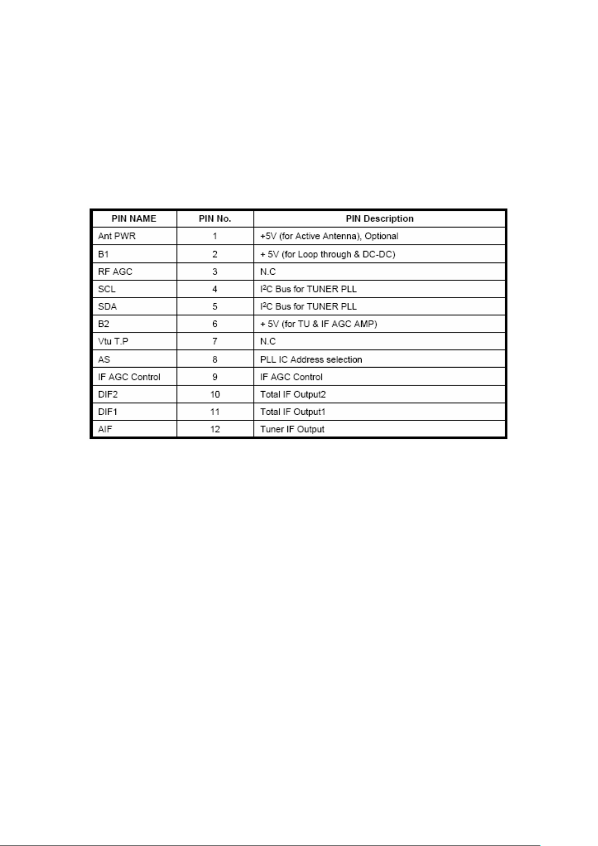
2.3. Pinning:
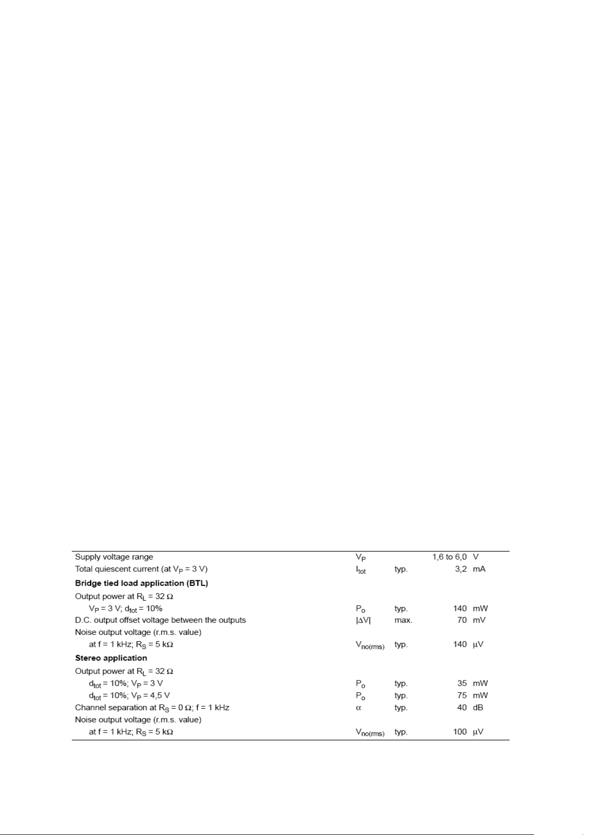
3. AUDIO AMPLIFIER STAGE WITH MP7722
3.1. General Description
17MB35 uses a 20W Class D Stereo Single Ended Audio Amplifer for audio. The
MP7722 is a stereo 20W Class D Audio Amplif
fully integrated audio amplifiers which dramatically reduces solution size by integrating
the following:
x 180mSRZHU026)(7V
x Startup / Shutdown pop elimination
x Short circuit protection
x Mute / Standby
The MP7722 utilizes a single ended output structure capable of delivering 2 x 20W into
4 speakers. MPS Class D Audio Amplifiers exhibit the high fidelity of a Class A/B
amplifier at efficiencies greater than 90%. The circuit is based on the MPS’ proprietary
variable frequency topology that delivers low distortion, fast response time and operates
on a single power supply.
3.2. Features
x 2 x 20W Output at VDD = 24V into a 4ORDG
x THD+N = 0.06% at 1W, 8
x 93% Efficiency at 20W
ier. It is one of MPS’ second generation of
Page 9
x Low Noise (190μV Typical)
x Switching Frequency Up to 1MHz
x 9.5V to 24V Operation from a Single Supply
x Integrated Startup and Shutdown Pop Elimination Circuit
x Thermal and Short Circuit Protection
x Integrated 180m6ZLWFKHV
x Mute/Standby Modes (Sleep)
x Thermally Enhanced 20-Pin TSSOP Package with Exposed Pad
3.3. Applications
x Surround Sound DVD Systems
x Televisions
x Flat Panel Monitors
x Multimedia Computers
x Home Stereo Systems
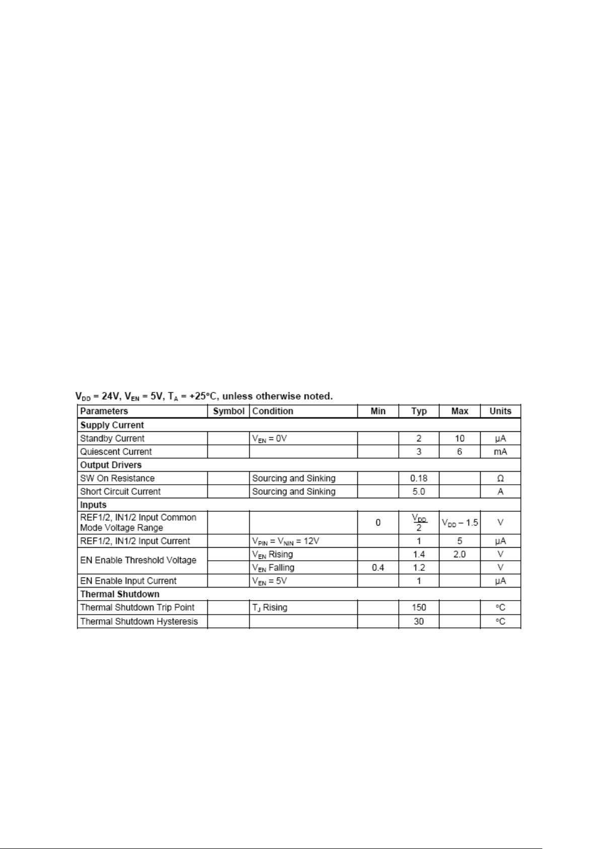
3.4. Absolute Ratings
3.4.1. Electrical Characteristics
Page 10
3.4.2. Operating Specifications
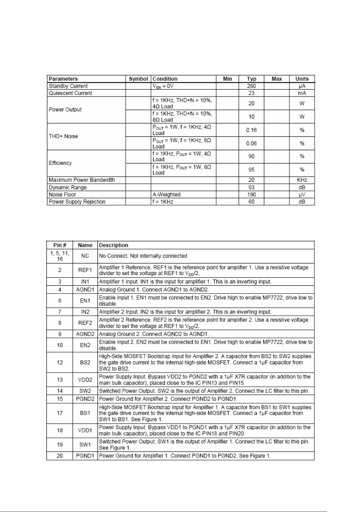
3.5. Pinning
Page 11

4. POWER STAGE
The DC voltages required at various parts of the chassis and inverters are provided by a
main power supply unit. The power supply generates 33V, 24V, 12V, 5V, 3,3V and 5V,
3,3V stand by mode DC voltages. Power stage which is on-chasis generates 1,26V
stand by voltage and 8V, 2,6V, 1,8V and 1V supplies for other different parts of the
chassis.
5. MICROCONTROLLER (MSTAR)
5.1. General Descripction
The MST6WB7GQ-3 is a high performance and fully integrated IC for multifunction LCD monitor/TV with resolutions up to full HD (1920x1080). It is
configured with an integrated triple-ADC/PLL, an integrated DVI/HDCP/HDMI
receiver, a multi-standard TV video and audio decoder, two video de-interlacers, two
scaling engines, the MStarACE-3 color engine, an on-screen display controller, an 8-bit
MCU and a built-in output panel interface. By use of external frame buffer, PIP/POP is
provided for multimedia applications. Furthermore, 3-D video decoding and processing
are fulfilled for high-quality TV applications. To further reduce system costs, the
MST6WB7GQ-3 also integrates intelligent power management control capability for
green-mode requirements and spread-spectrum support for EMI management.
5.2. General Features
LCD TV controller with PIP/POP display functions
x Input supports up to UXGA & 1080P
x Panel supports up to full HD (1920x1080)
x TV decoder with 3-D comb filter
x Multi-standard TV sound demodulator and decoder
x 10-bit triple-ADC for TV and RGB/YPbPr
x 10-bit video data processing
x Integrated DVI/HDCP/HDMI compliant receiver
x High-quality dual scaling engines & dual 3-D video de-interlacers
x 3-D video noise reduction
x Full function PIP/PBP/POP
x MStarACE-3 picture/color processing engine
x Embedded On-Screen Display (OSD) controler engine
x Built-in MCU supports PWM & GPIO
x Built-in dual-link 8/10-bit LVDS transmitter
x 5-volt tolerant inputs
x Low EMI and power saving features
x 296-pin LQFP
NTSC/PAL/SECAM Video Decoder
x Supports NTSC M, NTSC-J, NTSC-4.43, PAL (B,D,G,H,M,N,I,Nc), and SECAM
x Automatic TV standard detection
x Motion adaptive 3-D comb filter for NTSC/PAL
Page 12

x 8 configurable CVBS & Y/C S-video inputs
x Supports Teletext level-1.5, WSS, VPS, Closed-caption, and V-chip
x Macrovision detection
x CVBS video output
Video IF for Multi-Standard Analog TV
x Digital low IF architecture
x Stepped-gain PGA with 26 dB tuning range and 1 dB tuning resolution
x Maximum IF analog gain of 37dB in addition to digital gain
x Programmable TOP to accommodate different tuner gain to optimize noise and
linearity performance
Multi-Standard TV Sound Decoder
x Supports BTSC/NICAM/A2/EIA-J demodulation and decoding
x FM stereo & SAP demodulation
x L/Rx4, mono, and SIF audio inputs
x L/Rx3 loudspeaker and line outputs
x Supports sub-woofer output
x Built-in audio output DAC’s
x Audio processing for loudspeaker channel, including volume, balance, mute,
tone, EQ, and virtual stereo/surround
x Optional advanced surround available (Dolby1, SRS2, BBE3… etc)
Digital Audio Interface
x I2S digital audio input & output
x S/PDIF digital audio input & output
x HDMI audio channel processing capability
x Programmable delay for audio/video synchronization
Analog RGB Compliant Input Ports
x Three analog ports support up to UXGA
x Supports HDTV RGB/YPbPr/YCbCr
x Supports Composite Sync and SOG (Sync-on-Green) separator
x Automatic color calibration
DVI/HDCP/HDMI Compliant Input Port
x Two HDMI input ports with built-in switch
x Supports TMDS clock up to 225MHz @ 1080P 60Hz with 12-bit deep-color
resolution
x Single link on-chip DVI 1.0 compliant receiver
x High-bandwidth Digital Content Protection(HDCP) 1.1 compliant receiver
Page 13

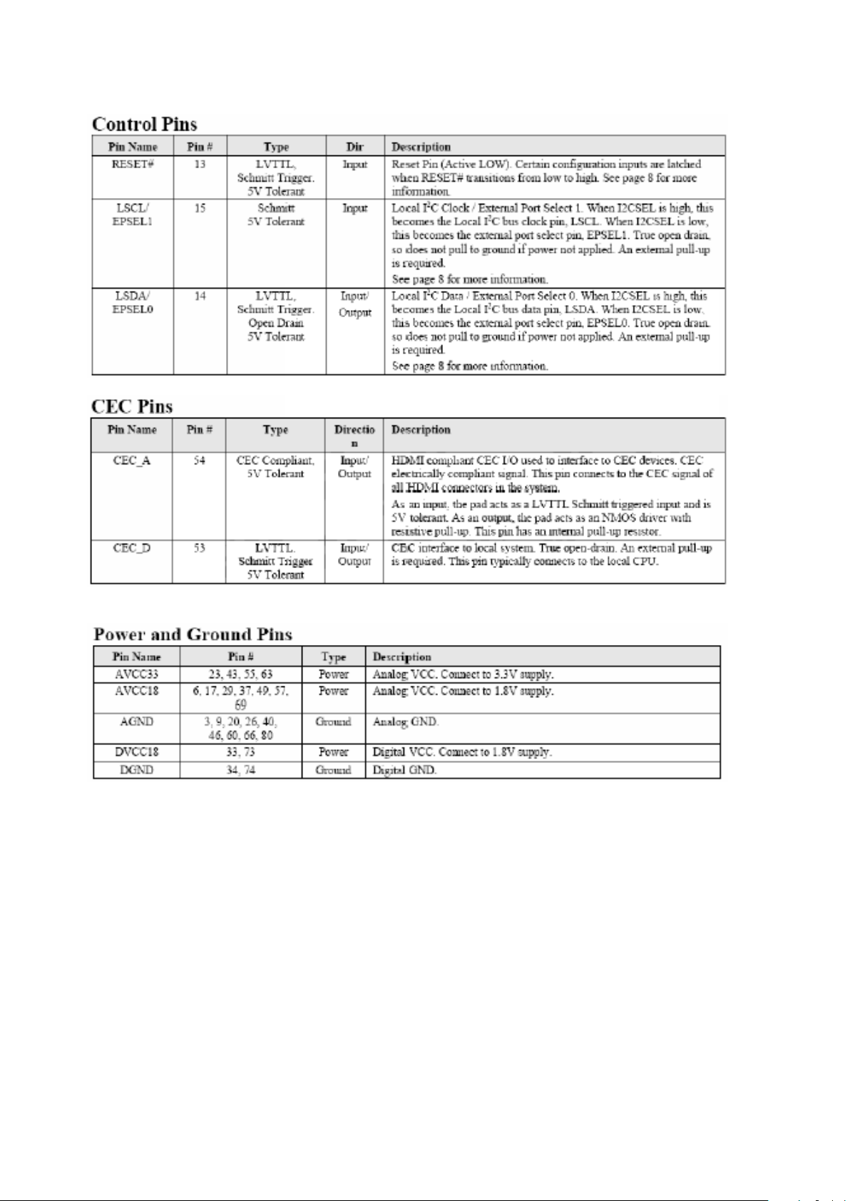
6. SIL9185 3:1 HDMI 1.3 Switch
6.1. General Desription
The SiI9185A is the first generation of TMDS switch device supporting Revision 1.3 of
the HDMI Specification (HDMI Consortium; June 2006). With three HDMI inputs and a
single output, the SiI9185A provides a low-cost method of adding additional HDMI ports
to the latest Digital TVs. New DTVs can easily connect to the many HDMI sources
coming on the market, including DVDs, STB, game consoles, PCs, camcorders, and
digital still cameras. The SiI9185A is a fully HDMI compliant device providing a simple,
lowcost method of retransmitting protected digital audio and video, giving end-users a
truly all-digital experience. Built-in backward compatibility with DVI 1.0 allows HDMI
systems to connect to any DVI 1.0 source. The SiI9185A provides additional integrated
features to help lower system cost and provide enhanced features to the end consumer.
To lower system cost, the SiI9185A provides a complete solution for switching sink-side
HDMI signals. This includes DDC switching, individual HPD control, and 5V sense. The
addition of these features eliminates additional external components, helping to lower
cost. For source-side applications, the SiI9185A DDC switching can be bypassed with
an external 4-channel I2C-bus switch(e.g., Texas Instruments PCA95445) to allow clock
stretching.
6.2. Features
x Three-input, single-output HDMI switcher
x Integrated TMDS® receiver and transmi
transmitting 2.25Gbps:
x Support 60Hz, 12-bit or 720p/1080i, 120Hz, 12-bit
x Buil
x Pre-emphasi
x DVI 1.0, HDCP 1.1 and HDMI compliant receiver and transmitter
x Uses HDMI-compliant TMDS core recovery and retransmission, unlike TMDS
x Built-in Cons support:
x HDM
x Integra
dable support even at deep-color resolutions
s
switches, which use high-spee
I lowers cost for adding CEC support to DTV
l requirements on system microcontroller speeds design
d analog switches and degrade TMDS signals
t cores capable of receiving and
6.3. Absolute Maximum Ratings
Page 14
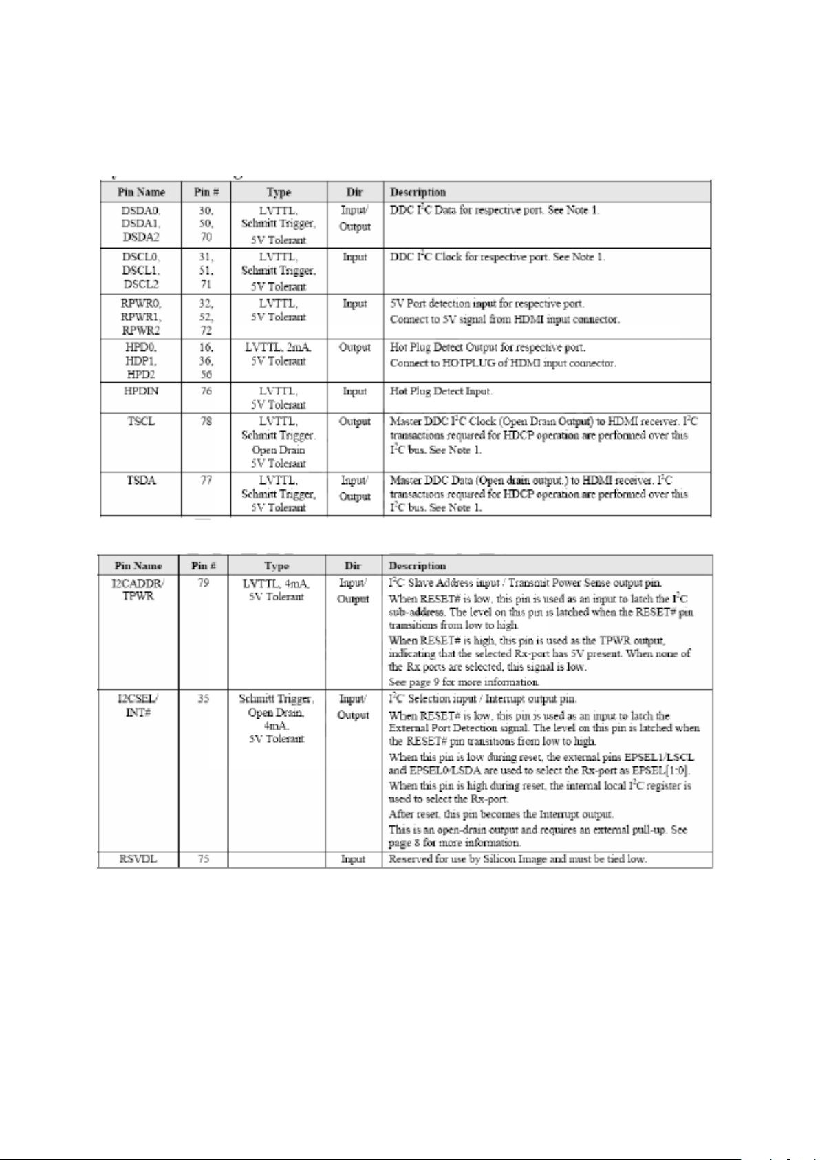
6.4. Pinning
Configuration Pins
Page 15
7. QAM DEMODULATOR – STV0297E
7.1. General Desription
The STV0297E is a complete single-chip QAM (quadrature amplitude modulation)
demodulation and FEC (forward error correction) solution that performs sampled IF to
transport stream (MPEG-2 or MPEG-4) block processing of QAM signals. It is intended
for the digital transmission of compressed television, sound, and data services over
cable. It is fully compliant with ITU-T J83 Annexes A/C or DVB-C specification
bitstreams (ETS 300 429, “Digital broadcasting systems for television, sound and data
services – Framing structure, channel coding and modulation - Cable Systems”). It can
handle square (16, 64, 256-QAM) and non-square (32, 128-QAM) constellations.
Page 16

Japanese DBS systems require a transport stream multiplex frame (TSMF) layer to
carry digital signals over cable systems. When the recovered transport stream is a
multiplex frame, the STV0297E post-processes it to extract a single transport stream.
Automatic detection of the TSMF layer is provided. The chip integrates an analog-todigital converter that delivers the required performance to handle up to 256-QAM signals
in a direct IF sampling architecture, thus eliminating the need for external
downconversion.
7.2. Features
x Decodes ITU-T J.83-Annexes A/C and DVB-C bit streams
x Processes Japanese transport stream multiplex frame (TSMF)
x High-performance integrated A/D converter suitable for direct IF architecture in all
QAM (quadrature amplitude modulation) modes
x Supports 16, 32, 64, 128 and 256 point constellations
x Small footprint package: (10 x 10 mm²)
x Very low power consumption
x Full digital demodulation
x Variable symbol rates
x Front derotator for better low symbol rate performance and relaxed tuner
constraints
x Integrated matched filtering
x Robust integrated adaptive pre and post equalizer
x On-chip FEC A/C with ability to bypass individual blocks
x 10 programmable GPIO
x Two AGC outputs suitable for delayed AGC applications (sigma-delta outputs)
x Integrated signal quality monitors, plus lock indicator and interrupt function
mapped to GPIO pin
x Improved signal acquisition
x System clock generated on-chip from quartz crystal
x Low frequency crystal operations 4, 16, 25 - 30 MHz
x 4 I2C addresses
x Easy control and monitoring via 2-wire fast I2C bus
7.3. Absolute Maximum Ratings
Page 17
7.4. Pinning
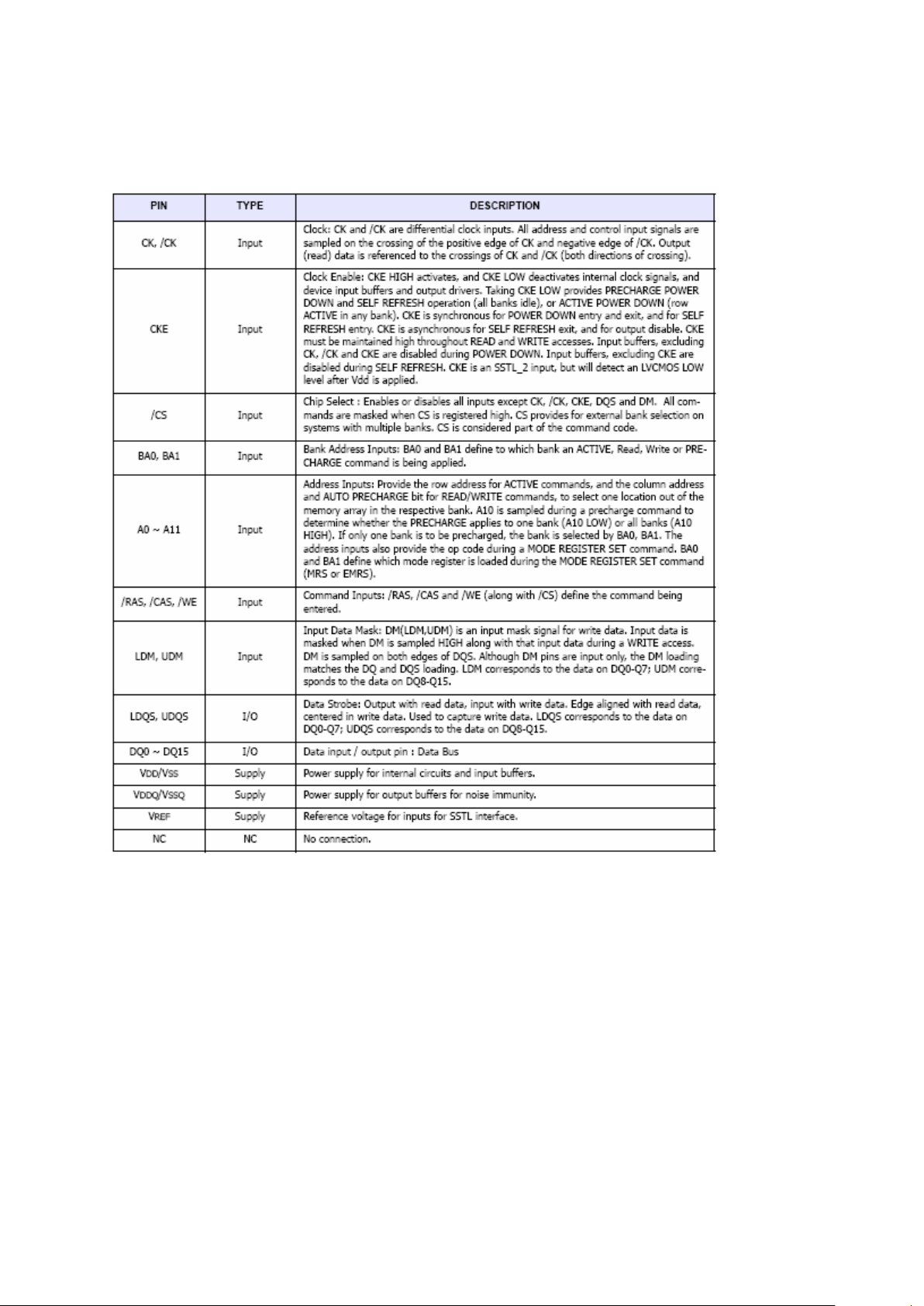
8. HY5DV281622DT-5 DDR SDRAM 128M
8.1. General Description
The Hynix HY5DV281622 is a 134,217,728-bit CMOS Double Data Rate(DDR)
Synchronous DRAM, ideally suited for the point-to-point applications which requires high
bandwidth. The Hynix 8Mx16 DDR SDRAMs offer fully synchronous operations
referenced to both rising and falling edges of the clock. While all addresses and control
inputs are latched on the rising edges of the CK (falling edges of the /CK), Data,Data
strobes and Write data masks inputs are sampled on both rising and falling edges of it.
The data paths are internally pipelined and 2-bit prefetched to achieve very high
bandwidth. All input and output voltage levels are compatible with SSTL_2.
Page 18
8.2. Features
x 3.3V for VDD and 2.5V for VDDQ power supply
x All inputs and outputs are compatible with SSTL_2 interface
x JEDEC standard 400mil 66pin TSOP-II with 0.65mm pin pitch
x Fully differential clock inputs (CK, /CK) operation
x Double data rate interface
x Source synchronous - data transaction aligned to bidirectional data strobe (DQS)
x x16 device has 2 bytewide data strobes (LDQS, UDQS) per each x8 I/O
x Data outputs on DQS edges when read (edged DQ) Data inputs on DQS centers
when write (centered DQ)
x Data(DQ) and Write masks(DM) latched on the both rising and falling edges of
the data strobe
x All addresses and control inputs except Data, Data strobes and Data masks
latched on the rising edges of the clock
x Write mask byte controls by LDM and UDM
x Programmable /CAS latency 3 / 4 supported
x Programmable Burst Length 2 / 4 / 8 with both sequential and interleave mode
x Internal 4 bank operations with single pulsed /RAS
x tRAS Lock-Out function supported
x Auto refresh and self refresh supported
x 4096 refresh cycles / 32ms
x Full, Half and Matched Impedance(Weak) strength driver option controlled by
EMRS
8.3. Absolute Maximum Ratings
Page 19
8.4. Pinning
9. IS42S16100C1 SDRAM
9.1. General Description
ISSI’s 16Mb Synchronous DRAM IS42S16100C1 is organized as a 524,288-word x 16bit x 2-bank for improved performance. The synchronous DRAMs achieve high-speed
data transfer using pipeline architecture. All inputs and outputs signals refer to the rising
edge of the clock input.
9.2. Features
x Clock frequency: 200, 166, 143 MHz
x Fully synchronous; all signals referenced to a positive clock edge
x Two banks can be operated simultaneously and independently
Page 20
x Dual internal bank controlled by A11 (bank select)
x Single 3.3V power supply
x LVTTL interface
x Programmable burst length (1, 2, 4, 8, full page)
x Programmable burst sequence:Sequential/Interleave
x 4096 refresh cycles every 64 ms
x Random column address every clock cycle
x Programmable CAS latency (2, 3 clocks)
x Burst read/write and burst read/single write operations capability
x Burst termination by burst stop and precharge command
x Byte controlled by LDQM and UDQM
x Industrial temperature up to 143 MHz
x Packages 400-mil 50-pin TSOP-II, 60-ball fBGA
x Lead-free package option
9.3. Pinning
10. SAW FILTER
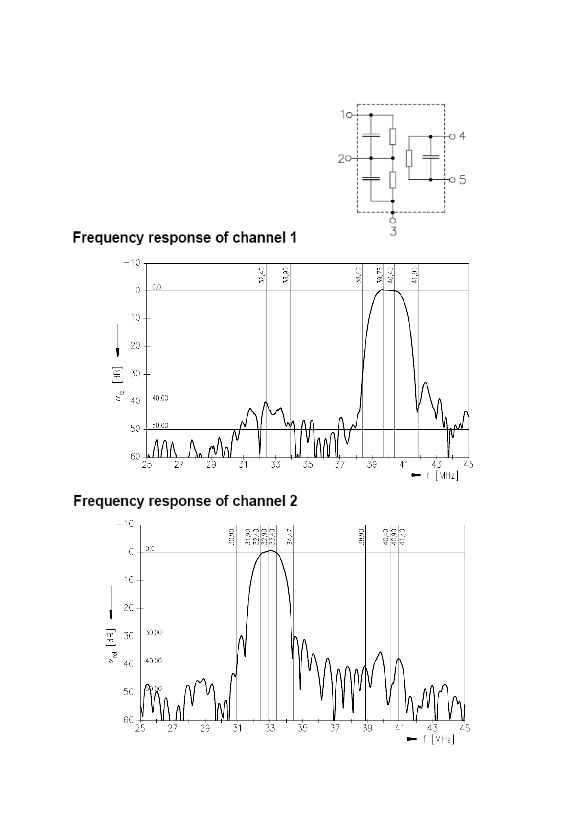
10.1. IF Filter for Audio Applications – Epcos K9656M
10.1.1. Standart:
x B/G
x D/K
x I
x L/L’
10.1.2. Features:
x TV IF audio filter with two channels
x Channel 1 (L’) with one pass band for sound carriers at 40,40 MHz (L’) and 39,75
MHz (L’- NICAM)
x Channel 2 (B/G,D/K,L,I) with one pass band for sound carriers between 32,35
MHz and 33,40 MHz
Page 21
10.1.3. Pin configuration:
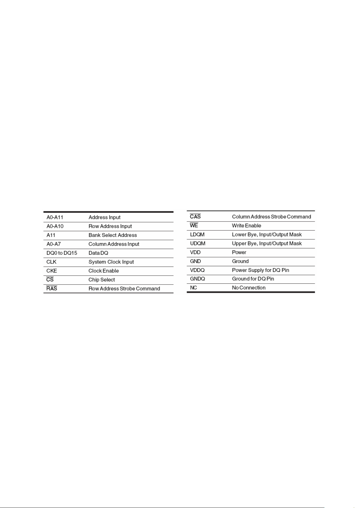
1 Input
2 Switching input
3 Chip carrier - ground
4 Output
5 Output
10.1.4. Frequency response:
Page 22
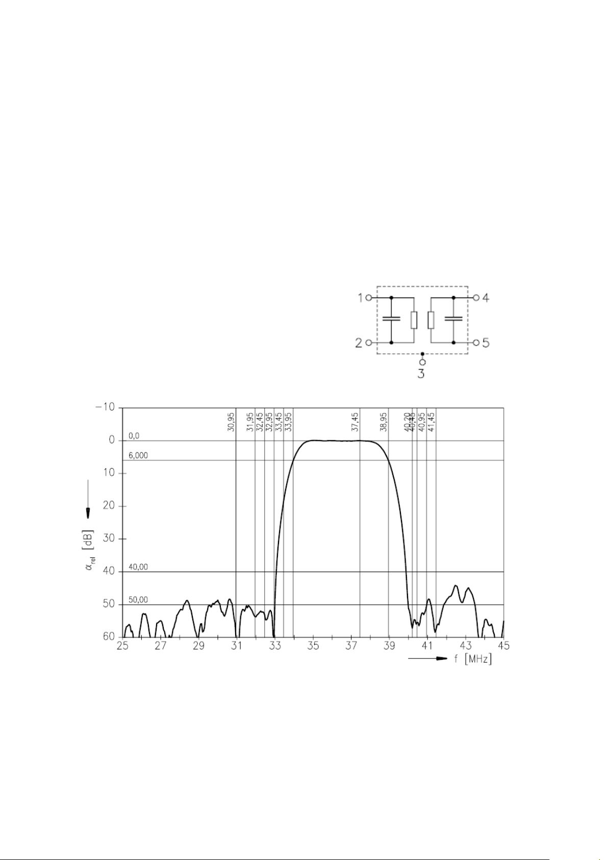
10.2. IF Filter for Video Applications – Epcos K3958M
10.2.1. Standart:
x B/G
x D/K
x I
x L/L’
10.2.2. Features:
x TV IF filter with Nyquist slopes at 33.90 MHz and 38.90 MHz
x Constant group delay
Pin configuration:
1 Input
2 Input - ground
3 Chip - carrier ground
4 Output
5 Output
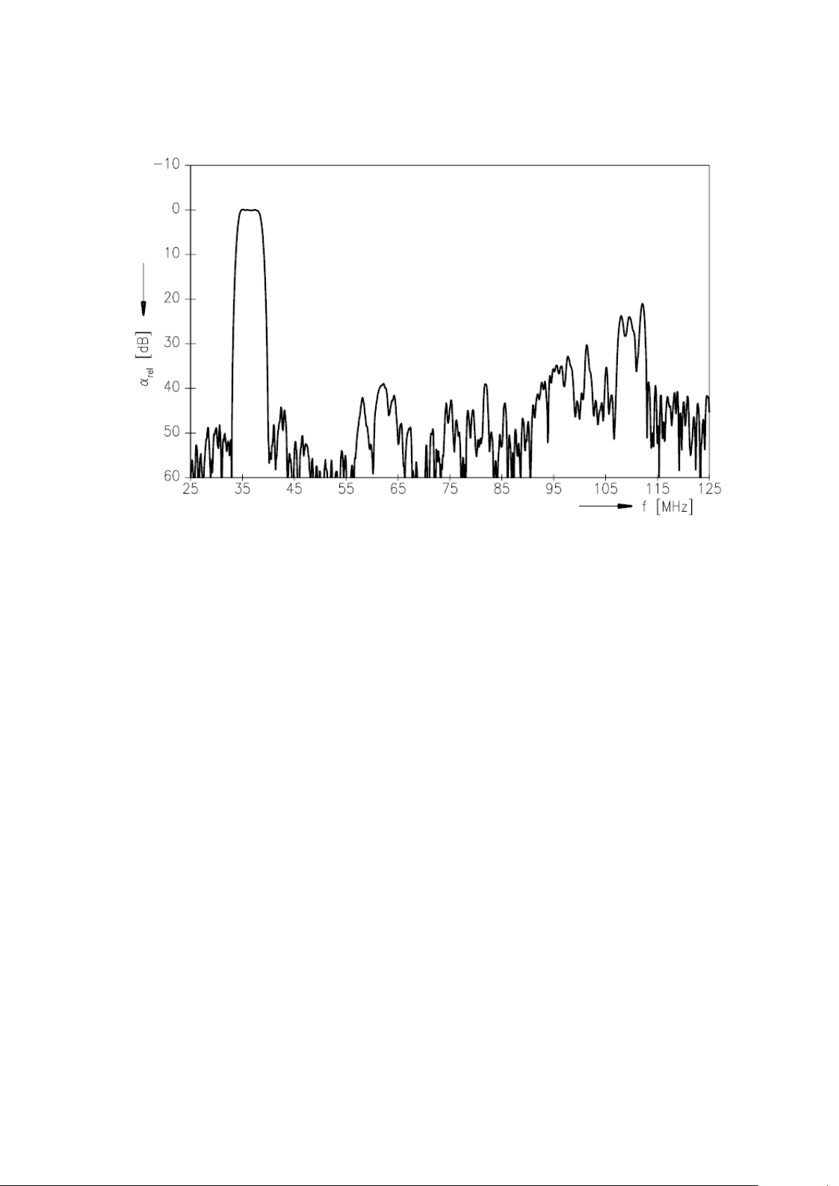
10.2.3. Frequency response:
Page 23
11. 2048-Bits Serial EEPROM – 24LC02
11.1. General Description
The 24LC01/02 is a 1K/2K-bit serial read/write non-volatile memory device using the
CMOS floating gate process. Its 1024/2048 bits of memory are organized into 128/256
words and each word is 8 bits. The device is optimized for use in many industrial and
commercial applications where low power and low voltage operation are essential. Up to
eight HT24LC01/02 devices may be connected to the same two-wire bus. The
HT24LC01/02 is guaranteed for 1M erase/write cycles and 40-year data retention.
11.2. Features
x Operating voltage: 2.4V~5.5V
x Low power consumption
x Operation: 5mA max.
x Standby: 5mA max.
x Internal organization
x 1K (HT24LC01):128´8
x 2K (HT24LC02): 256´8
x 2-wire serial interface
x Write cycle time: 5ms max.
x Automatic erase-before-write operation
x Partial page write allowed
x 8-byte Page write modes
x Write operation with built-in timer
x Hardware controlled write protection
Page 24
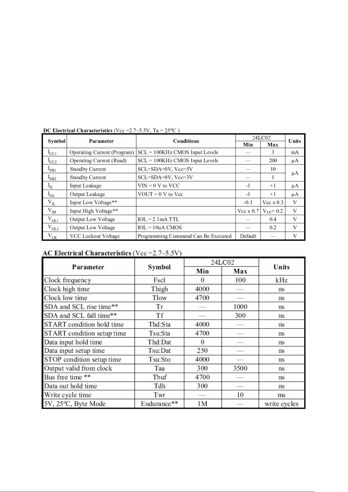
x 40-year data retention
x 106 erase/write cycles per word
x 8-pin DIP/SOP package
x 8-pin TSSOP (HT24LC02 only)
x Commerical temperature range (0°C to +70°C)
11.3. Electrical Specifications
Page 25
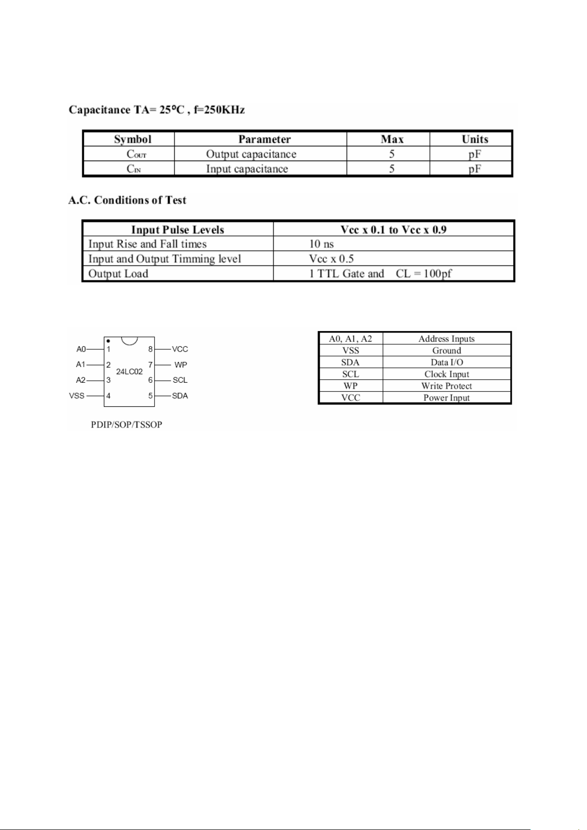
11.4. Pinning
12. 32K Smart Serial EEPROM – 24C32
12.1. General Description
The Microchip Technology Inc. 24C32 is a 4K x 8 (32K bit) Serial Electrically Erasable
PROM. This device has been developed for advanced, low power applications such as
personal communications or data acquisition. The 24C32 features an input cache for
fast write loads with a capacity of eight 8-byte pages, or 64 bytes. It also features a fixed
4K-bit block of ultra-high endurance memory for data that changes frequently. The
24C32 is capable of both random and sequential reads up to the 32K boundary.
Functional address lines allow up to eight 24C32 devices on the same bus, for up to
256K bits address space. Advanced CMOS technology makes this device ideal for lowpower non-volatile code and data applications. The 24C32 is available in the standard 8pin plastic DIP and 8-pin surface mount SOIC package.
12.2. Features
x Voltage operating range: 4.5V to 5.5V
x Peak write current 3 mA at 5.5V
x Maximum read current 150 μA at 5.5V
x Standby current 1 μA typical
x Industry standard two-wire bus protocol, I2C compatible
x Including 100 kHz and 400 kHz modes
Page 26
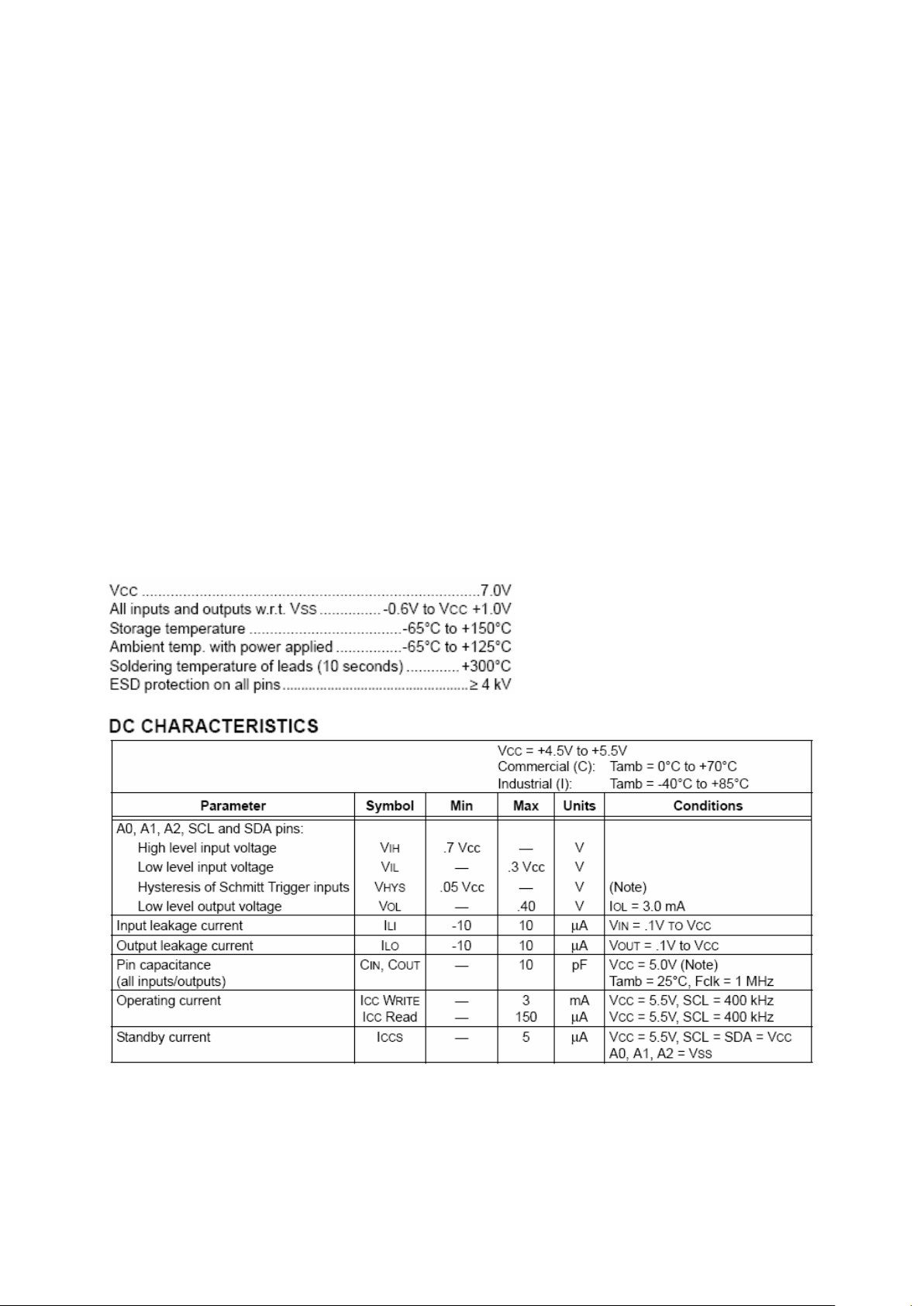
x Self-timed write cycle (including auto-erase)
x Power on/off data protection circuitry
x Endurance: 10,000,000 Erase/Write cycles guaranteed for High Endurance
Block, 1,000,000 E/W cycles guaranteed for Standard Endurance Block
x 8 byte page, or byte modes available
x 1 page x 8 line input cache (64 bytes) for fast write loads
x Schmitt trigger, filtered inputs for noise suppression
x Output slope control to eliminate ground bounce
x 2 ms typical write cycle time, byte or page
x Up to 8 chips may be connected to the same bus for up to 256K bits total
memory
x Electrostatic discharge protection > 4000V
x Data retention > 200 years
x 8-pin PDIP/SOIC packages
x Temperature ranges: Commercial (C): 0°C to +70°C, Industrial (I): -40°C to
+85°C
12.3 Absolute Maximum Ratings and Electrical Characteristics
Page 27
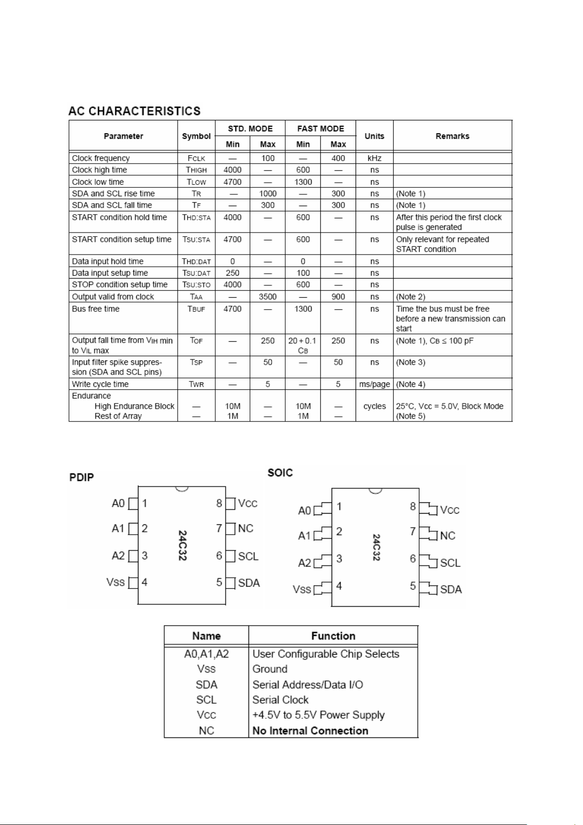
12.4 Pinning
Page 28

13. 512K CMOS Serial Flash – MX25L512
13.1. General Description
The MX25L512 is a CMOS 524,288 bit serial Flash memory, which is configured as
65,536 x 8 internally. The MX25L512 feature a serial peripheral interface and software
protocol allowing operation on a simple 3-wire bus. The three bus signals are a clock
input (SCLK), a serial data input (SI), and a serial data output (SO). SPI access to the
device is enabled by CS# input. The MX25L512 provide sequential read operation on
whole chip. After program/erase command is issued, auto program/ erase algorithms
which program/ erase and verify the specified page or sector/block locations will be
executed. Program command is executed on page (256 bytes) basis, and erase
command is executes on chip or sector (4K-bytes). To provide user with ease of
interface, a status register is included to indicate the status of the chip. The status read
command can be issued to detect completion status of a program or erase operation via
WIP bit. When the device is not in operation and CS# is high, it is put in standby mode
and draws less than 10uA DC current. The MX25L512 utilize MXIC's proprietary
memory cell, which reliably stores memory contents even after 100,000 program and
erase cycles.
13.2. Features
GENERAL
x Serial Peripheral Interface (SPI) compatible -- Mode 0 and Mode 3
x 524,288 x 1 bit structure
x 16 Equal Sectors with 4K byte each
x Any Sector can be erased individually
x Single Power Supply Operation
x 2.7 to 3.6 volt for read, erase, and program operations
x Latch-up protected to 100mA from -1V to Vcc +1V
x Low Vcc write inhibit is from 1.5V to 2.5V
PERFORMANCE
x High Performance
x Fast access time: 85MHz serial clock (15pF + 1TTL Load) and 66MHz serial
clock (30pF + 1TTL Load)
x Fast program time: 1.4ms(typ.) and 5ms(max.)/page (256-byte per page)
x Fast erase time: 60ms(typ.) and 120ms(max.)/sector (4K-byte per sector) ;
1s(typ.) and 2s(max.)/chip(512Kb)
x Low Power Consumption
x Low active read current: 12mA(max.) at 85MHz, 8mA(max.) at 66MHz and
4mA(max.) at 33MHz
x Low active programming current: 15mA (max.)
x Low active erase current: 15mA (max.)
x Low standby current: 10uA (max.)
x Deep power-down mode 1uA (typical)
x Minimum 100,000 erase/program cycles
Page 29
SOFTWARE FEATURES
x Input Data Format
x 1-byte Command code
x Block Lock protection
x The BP0~BP1 status bit defines the size of the area to be software protected
against Program and Erase instructions.
x Auto Erase and Auto Program Algorithm
x Automatically erases and verifies data at selected sector
x Automatically programs and verifies data at selected page by an internal
algorithm that automatically times the program pulse widths (Any page to be
programed should have page in the erased state first)
x Status Register Feature
x Electronic Identification
x JEDEC 2-byte Device ID
x RES command, 1-byte Device ID
HARDWARE FEATURES
x SCLK Input
x Serial clock input
x SI Input
x Serial Data Input
x SO Output
x Serial Data Output
x WP# pin
x Hardware write protection
x HOLD# pin pause the chip without diselecting the chip
x PACKAGE
x 8-pin SOP (150mil)
x All Pb-free devices are RoHS Compliant
13.3 Absolute Maximum Ratings
Page 30

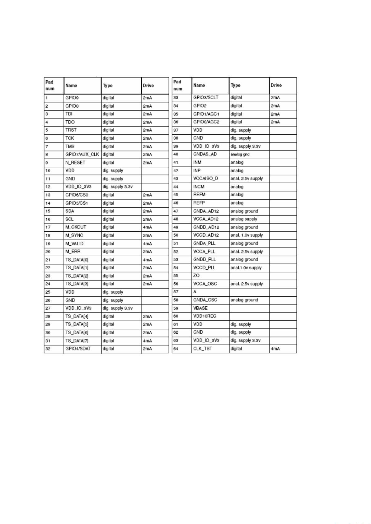
14. Integrated DVB-T Receiver
14.1 General Description
CT216T is a highly integrated single chip for DVB-T compliant STB solution. Compared
with Cheertek's previous generations of STB receiver devices. CT216T further interates
COFDM demodulator USB 2.0 HS host controller, memory card reader, 1/2-bit SPIFlash
interface, audio DAC, PWM in/out and SAR-ADC functions. In additiont special
enhangements are provided such as MPEG-4 video decoding, 16-bit OSD with anti-
Page 31

flickering, HW JPEG decoding, flesh tone and black-white extensions, and improvement
of small video quality.
CT216T includes COFDM demodulator transport stream de-multiplexer, DVB-CSA
compliant de-scrambler, RISC MPUs, MPEG-1/2/4 AV decoder, digital T\/ encoder,
audio DACs, USB 2.0 HS host controller, memory card reader, smart card reader, CI
controller and other peripherals.
Cli216T is designed in focus on the market of single tuner input product which makes, it
a cost effective solution. Supports include free to air, conditional access for SC (Smart
card) and CI portable devices, PVR, LCD TV, and other DVB-T applications.
14.2 Features
COFDM Demodulator
x ETSI EN 300 744 DVB-T NorDig Unified 1.0.3, and D-book compliant
x Automatic spectral inversion, detection
x Integrated ADC
x Direct IF (36.167 MHz or 43.75 MHz) or low IF (4.57 MHz) supported
x Single IF AGC or dual RF/lF AGC controls with ǻȈ modulabon
x Impulsive noise cancellation
x Carrier acquisition range: ±400 kHz (extensible to ±600 kHz in 8MHz BW)
x Adjacent channel interference (ACI) filter,for supporting 6, 7, and 8MHz channels
with one 8MHz analog filter
x Co-channel interterence (CCl) supression
x RF signal strength monitor
MPU
x Three 32-bit RISC MPU run up to 166MHz with total 448DMIPS
x 8KB I-Cache and 8KB D-Cache
x Two general purpose timers
x Watchdog timer
x DSU for source level debug
Memory
x 6-bit SDRAM controller supports up to 32MB (16MB for l28-pin)
x Unified memory architecture
x Parallel flash (216-pin only)
x 1/2-bit SPI flash
Transport De-multiplexing
x TS, PES, and ES demultiplexing
x OneTS path
x CI CAM interface (216-pin only)
x 32 general purpose PID filters
x 32 Section filters
x CRC-32 accelerator
Page 32

x DVB-CSA de-scramblers
Video Decoding and Processing
x MPEG-2 MP@ML
x MPEG-4 SP&ASP
x PAL/NTSC format conversion
x 3:2 pull down
x Zoom in/out from 1/16X to 16X
x HW JPEG decode
x 4/8/16-bit OSD with anti-flickering
x On chip NTSC/PAL TV encoder
x CVBS, S-VHS, and component video
x VBI insertion for Teletext, CC and WSS
x ITU-R BT.601 and ITU-R BT.656 outputs
x Flesh tone extension
x Black/white extension,
Audio Decoding and Processing
x MPEG-1: layer 1/2/3
x MPEG-2: layer 1/2
x Decode MPEG-2 and MPEG-1 audio at sampling frequency of 16K, 22.05K, 24K,
32K, 44.1K, and 48KHz
x Decode CU-DA at sampling frequency of 44.1 KHz
x SPDIF out for AC-3 by-pass
x Embedded 2 channels audio DAC for L/R outputs
x Digital mute control and volume adjustment
OSD(On Screen Display)
x There are total 9 display planes: border; background. video. RS1 (Rectangle Strip
1), RS2, OSD, RS3, RS4, and cursor.
x 4/8l16-bit OSD with anti-flickering and anti-flutter
x Support alpha-blending per color
x Adjustable brightness control in window
x Bitmap OSD
x Support horizontal pixel duplication to enlarge bitmap automatically
x Support sub-region redraw to facilitate bitmap display.
Digitnal TV Encoder
x NTSC-M, PAL-B, D, G, H, I, Nc, M encoding
x Four video DACs to provide 6 configuration output: modes
x Support CVBS, S-VHS. and component video outs
x VBI insertion for Teletext, CC and WSS
x Color burst amplitude control
x Programmable sync. level
x On chip, color-bar generator
Page 33

High Speed I/O
x USB 2.0 HS host controller
x Memory card reader with SD, MMC, and MS interfaces
x Compliant with SD spec. 1.1 and MMC spec. 4.0 with 1-bit & 4-bit modes.
x Compliant with Memory Stick Pro format spec. 1.02 and Memory stick format
spec 1.43 with 1-bit and 4-bit modes.
Peripherals
x Up to 3 full duplex UART with 16-byte FIFO
x 2-wire serial (2WS) in master mode .. .
x Up to 2 IS0-7816 compliant SC (1 in 128-pin, can also be used as UART)
x 5 digits 7-Segrnent LED control
x 5x3 two-dimension key scan
x 2 SAR-ADC input
x 4 PWM input/output
x 1 HW IR command decode
x GPIO
Electrical and Physical Characteristics
x Capable of using single 27MHz clock input crystal
x 1.8V and 3.3V dual power supply
x Power standby mode
x PQFP-128 (CT216T-Z) or LQFP-216 (CT216T-R) package
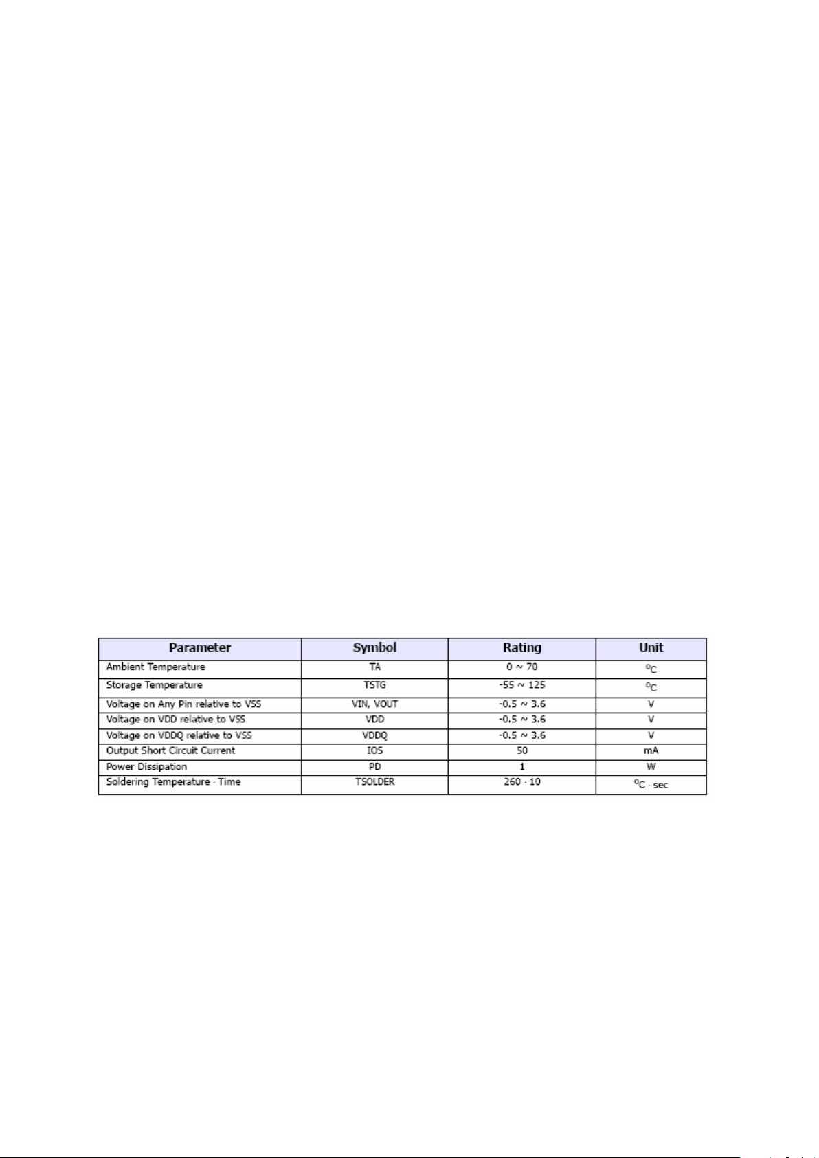
13.3 Absolute Maximum Rating and Electrical Characteristics
Page 34

Page 35

15. IC DESCRIPTIONS
15.1. LM1117
15.1.1. General Description
The LM1117 is a series of low dropout voltage regulators with a dropout of 1.2V at
800mA of load current. It has the same pin-out as National Semiconductor’s industry
standard LM317. The LM1117 is available in an adjustable version, which can set the
output voltage from 1.25V to 13.8V with only two external resistors. In addition, it is also
available in five fixed voltages, 1.8V, 2.5V, 2.85V, 3.3V, and 5V. The LM1117 offers
current limiting and thermal shutdown. Its circuit includes a zener trimmed bandgap
reference to as-sure output voltage accuracy to within ±1%. The LM1117 series is
available in SOT- 223, TO-220, and TO-252 D-PAK p
tantalum capacitor is required at the output to improve the transient response and
stability.
15.1.2. Features
x Available in 1.8V, 2.5V, 2.85V, 3.3V, 5V, and Adjustable Versions
x Space Saving SOT-223 Package
x Current Limiting and Thermal Protection
x Output Current 800mA
x Line Regulation 0.2% (Max)
x Load Regulation 0.4% (Max)
x Temperature Range
x LM1117 0°C to 125°C
x LM1117I -40°C to 125°C
DFNDJHV $ PLQLPXP RI ȝ)
15.1.3. Applications
x 2.85V Model for SCSI-2 Active Termination
x Post Regulator for Switching DC/DC Converter
x High Efficiency Linear Regulators 15
x 32” TFT TV Service Manual 10/01/2005
x Battery Charger
x Battery Powered Instrumentation
15.1.4. Absolute Maximum Ratings
Page 36

15.1.5. Pinning
15.2. 74HCT4053
15.2.1. General Description
The 74HC4053; 74HCT4053 is a high-speed Si-gate CMOS device and is pin
compatible with the HEF4053B. It is specified in compliance with JEDEC standard no.
7A. The 74HC4053; 74HCT4053 is triple 2-channel analog multiplexer/demultiplexer
with a common enable input (E). Each multiplexer/demultiplexer has two independent
inputs/outputs (nY0 and nY1), a common input/output (nZ) and three digital select inputs
(Sn). With E LOW, one of the two switches is selected (low-impedance ON-state) by S1
to S3. With E HIGH, all switches are in the high-impedance OFF-state, independent of
S1 to S3. VCC and GND are the supply voltage pins for the digital control inputs (S1 to
S3 and E). The VCC to GND ranges are 2.0 V to 10.0 V for 74HC4053 and 4.5 V to 5.5
V for 74HCT4053. The analog inputs/outputs (nY0 and nY1, and nZ) can swing between
VCC as a positive limit and VEE as a negative limit. VCC - VEE may not exceed 10.0 V.
For operation as a digital multiplexer/demultiplexer, VEE is connected to GND (typically
ground).
15.2.2. Features
x Low ON resistance:
x 80 W (typical) at VCC - VEE = 4.5 V
x 70 W (typical) at VCC - VEE = 6.0 V
x 60 W (typical) at VCC - VEE = 9.0 V
x Logic level translation:
x To enable 5 V logic to communicate with ±5 V analog signals
x Typical ‘break before make’ built in
x Complies with JEDEC standard no. 7A
x ESD protection: HBM EIA/JESD22-A114-C exceeds 2000 V, MM
EIA/JESD22-A115-A exceeds 200 V
x Multiple package options
x Specified from -40 °C to +85 °C and from -40 °C to +125 °C
15.2.3. Applications
x Analog multiplexing and demultiplexing
x Digital multiplexing and demultiplexing
x Signal gating
Page 37

15.2.4. Absolute Maximum Ratings
15.2.5. Pinning
15.3. NUP4004M5
15.3.1. General Description
This 5-Pin bi-directional transient suppressor array is designed for applications requiring
transient overvoltage protection capability. It is intended for use in transient voltage and
Page 38

ESD sensitive equipment such as computers, printers, cell phones, medical equipment,
and other applications. Its integrated design provides bi-directional protection for four
separate lines using a single TSOP-5 package. This device is ideal for situations where
board space is a premium.
15.3.2. Features
x Bi-directional Protection for Four Lines in a Single TSOP-5 Package
x Low Leakage Current
x Low Capacitance
x Provides ESD Protection for JEDEC Standards JESD22
x Machine Model = Class C
x Human Body Model = Class 3B
x Provides ESD Protection for IEC 61000-4-2, 15 kV (Air), 8 kV (Contact)
x This is a Pb-Free Device
15.3.3. Absolute Maximum Ratings
15.3.4. Pinning
Page 39

15.4. FDN336P
15.4.1. General Description
The ST24LC21 is a 1K bit electrically erasable programmable memory (EEPROM),
organized by 8 bits.This device can operate in two modes: Transmit Only mode and I2C
bidirectional mode. When powered, the device is in Transmit Only mode with EEPROM
data clocked out from the rising edge of the signal applied on VCLK. The device will
switch to the I2C bidirectional mode upon the falling edge of the signal applied on SCL
pin. The ST24LC21 cannot switch from the I2C bidirectional mode to the Transmit Only
mode (except when the power supply is removed). The device operates with a power
supply value as low as 2.5V. Both Plastic Dual-in-Line and Plastic Small Outline
packages are available.
15.4.2. Features
x 1 MILLION ERASE/WRITE CYCLES
x 40 YEARS DATA RETENTION
x 2.5V to 5.5V SINGLE SUPPLY VOLTAGE
x 400k Hz COMPATIBILITY OVER the FULL RANGE of SUPPLY VOLTAGE
x TWO WIRE SERIAL INTERFACE I2C BUS COMPATIBLE
x PAGE WRITE (up to 8 BYTES)
x BYTE, RANDOM and SEQUENTIAL READ MODES
x SELF TIMED PROGRAMMING CYCLE
x AUTOMATIC ADDRESS INCREMENTING
x ENHANCED ESD/LATCH UP PERFORMANCES
15.4.3. Absolute Maximum Ratings
15.4.4. Pinning
Page 40

15.5. TL062 -
15.5.1. General Description
Low-power JFET-input operational amplifier
15.5.2. Features
x Very Low Power Consumption
x Typical Supply Current . . . 200 μA (Per Amplifier)
x Wide Common-Mode and Differential Voltage Ranges
x Low Input Bias and Offset Currents
x Common-Mode Input Voltage Range Includes VCC+
x Output Short-Circuit Protection
x High Input Impedance . . . JFET-Input Stage
x Internal Frequency Compensation
x Latch-Up-Free Operation
x High Slew Rate . . . 3.5 V/μs Typ
15.5.3. Absolute Maximum Ratings
Page 41

15.5.4. Pinning
15.6. PI5V330
15.6.1. General Description
Pericom Semiconductor.s PI5V series of mixed signal video circuits are produced in the
Company.s advanced CMOS low-power technology, achieving industry leading
performance. The PI5V330 is a true bidirectional Quad 2-channel
multiplexer/demultiplexer that is recommended for both RGB and composite video
switching applications. The VideoSwitch. can be driven from a current output RAMDAC
or voltage output composite video source. Low ON-resistance and wide bandwidth
make it ideal for video and other applications. Also this device has exceptionally high
current capability which is far greater than most analog switches offered today. A single
5V supply is all that is required for operation. The PI5V330 offers a high-performance,
low-cost solution to switch between video sources. The application section describes the
PI5V330 replacing the HC4053 multiplier and buffer/amplifier.
15.6.2. Features
x High-performance, low-cost solution to switch between video sources
x Wide bandwidth: 200 MHz
x Low ON-resistance: 3
x Low crosstalk at 10 MHz: .58 dB
x Ultra-low quiescent power (0.1 μA typical)
x Single supply operation: +5.0V
x Fast switching: 10 ns
x High-current output: 100 mA
x Packages available:
x 16-pin 300-mil wide plastic SOIC (S)
x 16-pin 150-mil wide plastic SOIC (W)
x 16-pin 150-mil wide plastic QSOP (Q)
15.6.3. Absolute Maximum Ratings
Page 42

15.6.4. Pinning
15.7. AZC099-04S
15.7.1. General Description
AZC099-04S is a high performance and low cost design which includes surge rated
diode arrays to protect high speed data interfaces. The AZC099-04S family has been
specifically designed to protect sensitive components, which are connected to data and
transmission lines, from over-voltage caused by Electrostatic Discharging (ESD),
Electrical Fast Transients (EFT), and Lightning.
AZC099-04S is a unique design which includes surge rated, low capacitance steering
diodes and a unique design of clamping cell which is an equivalent TVS diode in a
single package. During transient conditions, the steering diodes direct the transient to
either the power supply line or to the ground line. The internal unique design of clamping
cell prevents over-voltage on the power line, protecting any downstream components.
AZC099-04S may be used to meet the ESD immunity requirements of IEC 61000-4-2,
Level 4 (± 15kV air, ±8kV contact discharge).
15.7.2. Features
x ESD Protect for 4 high-speed I/O channels
x Provide ESD protection for each channel to IEC 61000-4-2 (ESD) ±15kV (air),
±8kV (contact) IEC 61000-4-4 (EFT) (5/50ns) Level-3, 20A for I/O, 40A for Power
IEC 61000-4-5 (Lightning) 4A (8/20ȝV
x 5V operating voltage /RZFDSDFLWDQFHS)W\SLFDO
x Fast turn-on and Low clamping voltage
x Array of surge rated diodes with internal equivalent TVS diode
x Small package saves board space
x Solid-state silicon-avalanche and active circuit triggering technology
Page 43

15.7.3. Absolute Maximum Ratings
15.7.4. Pinning
15.8. TDA1308
15.8.1. General Description
The TDA1308; TDA1308A is an integrated class-AB stereo headphone driver contained
in an SO8, DIP8 or a TSSOP8 plastic package. The TDA1308AUK is available in an 8
bump wafer level chip-size package (WLCSP8). The device is fabricated in a 1 mm
Complementary Metal Oxide Semiconductor (CMOS) process and has been primarily
developed for portable digital audio applications. The difference between the TDA1308
and the TDA1308A is that the TDA1308A can be used at low supply voltages.
15.8.2. Features
x Wide temperature range
x No switch ON/OFF clicks
x Excellent power supply ripple rejection
x Low power consumption
x Short-circuit resistant
x High performance
x High signal-to-noise ratio
Page 44

x High slew rate
x Low distortion
x Large output voltage swing
15.8.3. Absolute Maximum Ratings
15.8.4. Pinning
15.9. ST3222
15.9.1. General Description
The ST3222 is a 3V powered EIA/TIA-232 and V.28/V.24 communications interface with
low power requirements and high data-rate capabilities. ST3222 has a proprietary low
dropout transmitter output stage providing true RS-232 performance from 3 to 3.6V
power supplies. The device requires only four small 0.1mF standard external capacitors
for operating from 3V supply. The ST3222 has two receivers and two drivers. The
ST3222 features a 1mA shutdown mode that reduces power consumption and extends
battery life in portable systems. Its receivers can remain active in shutdown mode,
allowing external devices such as modems to be monitored using only 1mA supply
current. The device is guaranteed to run at data rates of 250Kbps while maintaining RS232 output levels.
15.9.2. Features
x 300mA SUPPLY CURRENT
x 250Kbps MINIMUM GUARENTEED DATA RATE
x 6V/ms MINIMUM GUARANTEED SLEW RATE
x MEET EIA/TIA-232 SPECIFICATIONS DOWN TO 3V
x AVAILABLE IN SO-18 AND TSSOP20
Page 45

15.9.3. Absolute Maximum Ratings
15.9.4. Pinning
15.10. LM358D
15.10.1. General Description
The LM158 series consists of two independent, high gain, internally frequency
compensated operational amplifiers which were designed specifically to operate from a
Page 46

single power supply over a wide range of voltages. Operation from split power supplies
is also possible and the low power supply current drain is independent of the magnitude
of the power supply voltage. Application areas include transducer amplifiers, dc gain
blocks and all the conventional op amp circuits which now can be more easily
implemented in single power supply systems. For example, the LM158 series can be
directly operated off of the standard +5V power supply voltage which is used in digital
systems and will easily provide the required interface electronics without requiring the
additional ±15V power supplies. The LM358 and LM2904 are available in a chip sized
package (8-Bump micro SMD) using National’s micro SMD package technology.
15.10.2. Features
x Available in 8-Bump micro SMD chip sized package,
x Internally frequency compensated for unity gain
x Large dc voltage gain: 100 dB
x Wide bandwidth (unity gain): 1 MHz (temperature compensated)
x Wide power supply: Single supply: 3V to 32V or dual supplies: ±1.5V to ±16V
x Low supply current drain (500 μA)—essentially independent of supply voltage
x Low input offset voltage: 2 mV
x Input common-mode voltage range includes ground
x Differential input voltage range equal to the power supply voltage
x Large output voltage swing
15.10.3. Absolute Maximum Ratings
Page 47

15.10.4. Pinning
15.11. 74LCX244
15.11.1. General Description
The LCX244 contains eight non-inverting buffers with 3-STATE outputs. The device may
be employed as a memory address driver, clock driver and bus-oriented
transmitter/receiver. The LCX244 is designed for low voltage (2.5V or 3.3V) VCC
applications with capability of interfacing to a 5V signal environment. The LCX244 is
fabricated with an advanced CMOS technology to achieve high speed operation while
maintaining CMOS low power dissipation.
15.11.2. Features
x 5V tolerant inputs and outputs
x 2.3V to 3.6V VCC specifications provided
x 6.5ns Tpd max. (VCC=3.3V), 10μA ICCmax.
x Power down high impedance inputs and outputs
x Supports live insertion/withdrawal
x ±24mA output drive (VCC=3.0V)
x Implements patented noise/EMI reduction circuitry
x Latch-up performance exceeds 500mA
x ESD performance:Human body model>2000V, Machine model>200V
x Leadless DQFN package
15.11.3. Absolute Maximum Ratings
Page 48

15.11.4. Pinning
15.12. 74LCX245
15.12.1. General Description
The LCX245 contains eight non-inverting bidirectional buffers with 3-STATE outputs and
is intended for bus oriented applications. The device is designed for low voltage (2.5V
and 3.3V) VCC applications with capability of interfacing to a 5V signal environment.
The T/R input determines the direction of data flow through the device. The OE input
disables both the A and B ports by placing them in a high impedance state.
The LCX245 is fabricated with an advanced CMOS technology to achieve high speed
operation while maintaining CMOS low power dissipation.
15.12.2. Features
x 5V tolerant inputs and outputs
x 2.3V to 3.6V VCC specifications provided
x 7.0ns tPDmax. (VCC=3.3V), 10μA ICCmax.
x Power down high impedance inputs and outputs
x Supports live insertion/withdrawal
x ±24mA output drive (VCC=3.0V)
x Implements patented noise/EMI reduction circuitry
x Latch-up performance exceeds 500mA
x ESD performance: Human body model>2000V, Machine model>200V
x Leadless DQFN package
Page 49

15.12.3. Absolute Maximum Ratings
15.12.4. Pinning
15.13. FSA3157
15.13.1. General Description
The NC7SB3157 / FSA3157 is a high-performance, single- pole / double-throw (SPDT)
analog switch or 2:1 multiplexer/ de-multiplexer bus switch. The device is fabricated with
advanced sub-micron CMOS technology to achieve high-speed enable and disable
times and low on resistance. The break-beforemake select circuitry prevents disruption
of signals on the B Port due to both switches temporarily being enabled during select pin
switching. The device is specified to operate over the 1.65 to 5.5V VCC operating range.
Page 50

The control input tolerates voltages up to 5.5V, independent of the VCC operating
range.
15.13.2. Features
x Useful in both analog and digital applications
x Space-saving, SC70 6-lead surface mount package
x Ultra-small, MicroPak™ Pb-free leadless package
x /RZ2Q5HVLVWDQFHȍRQW\SLFDODW99&&
x Broad VCC operating range: 1.65V to 5.5V
x Rail-to-rail signal handling
x Power-down, high-impedance control input
x Over-voltage tolerance of control input to 7.0V
x Break-before-make enable circuitry
x 250 MHz, 3dB bandwidth
15.13.3. Absolute Maximum Ratings
15.13.4. Pinning
Page 51

15.14. FMS6145
15.14.1. General Description
The FMS6145 Low-Cost Video Filter (LCVF) is intended to replace passive LC ¿OWHUV
and drivers with a low-cost integrated device. Five 4th-order ¿OWHUV provide improved
image quality compared to typical 2nd or 3rd-order passive solutions. The FMS6145
may be directly driven by a DC-coupled DAC output or an AC-coupled signal. Internal
diode clamps and bias circuitry may be used if AC-coupled inputs are required. The
outputs can drive AC- or DC-FRXSOHGVLQJOHȍRU GXDOȍORDGV'&FRXSOLQJWKH
outputs removes the need for output coupling capacitors. The input DC levels are offset
approximately +280mV at the output.
15.14.2. Features
x Five 4th-order 8MHz (SD) ¿OWHUV
x Drives single,AC- or DC-FRXSOHGYLGHRORDGV9SSȍ
x Drives dual, AC- or DC-FRXSOHGYLGHRORDGV9SSȍ
x Transparent input clamping
x AC- or DC-coupled inputs
x AC- or DC-coupled outputs
x DC-coupled outputs eliminate AC-coupling capacitors
x 5V only
x Robust 8kV ESD protection
x Lead-free TSSOP-14 package
15.14.3. Absolute Maximum Ratings
15.14.4. Pinning
Page 52

15.15. MT48LC4M16A2TG8E
15.15.1. General Description
The 64Mb SDRAM is a high-speed CMOS, dynamic random-access memory containing
67,108,864 bits. It is internally configured as a quad-bank DRAM with a synchronous
interface (all signals are registered on the positive edge of the clock signal, CLK). Each
of the x4’s 16,777,216-bit banks is organized as 4,096 rows by 1,024 columns by 4 bits.
Each of the x8’s 16,777,216-bit banks is organized as 4,096 rows by 512 columns by 8
bits. Each of the x16’s 16,777,216-bit banks is organized as 4,096 rows by 256 columns
by 16 bits. Read and write accesses to the SDRAM are burst oriented; accesses start at
a selected location and continue for a programmed number of locations in a
programmed sequence. Accesses begin with the registration of an ACTIVE command,
which is then ollowed by a READ or WRITE command. The address bits registered
coincident with the ACTIVE command are used to select the bank and row to be
accessed (BA0, BA1 select the bank; A0-A11 select the row).
15.15.2. Features
x PC66-, PC100- and PC133-compliant
x 143 MHz, graphical 4 Meg x 16 option
x Fully synchronous; all signals registered on positive edge of system clock
x Internal pipelined operation; column address can be changed every clock cycle
x Internal banks for hiding row access/precharge
x Programmable burst lengths: 1, 2, 4, 8 or full page
x Auto Precharge, includes CONCURRENT AUTO PRECHARGE, and AutO
Refresh Modes
x Self Refresh Modes: standard and low power
x 64ms, 4,096-cycle refresh
x LVTTL-compatible inputs and outputs
x Single +3.3V ±0.3V power supply
15.15.3. Absolute Maximum Ratings
Page 53

15.15.4. Pinning
15.16. MP1583
15.16.1. General Description
The MP1583 is a step-down regulator with a built in internal Power MOSFET. It
achieves 3A continuous output current over a wide input supply range with excellent
load and line regulation.
Current mode operation provides fast transient response and eases loop stabilization.
Fault condition protection includes cycle-by-cycle current limiting and thermal shutdown.
Adjustable soft-start reduces the stress on the input source at turn-on. In shutdown
mode the regulator draws 20μA of supply current.
The MP1583 requires a minimum number of readily available external components to
complete a 3A step down DC to DC converter solution.
Page 54

15.16.2. Features
x 3A Output Current
x Programmable Soft-Start
x 100m,QWHUQDO3RZHU026)(76ZLWFK
x Stable with Low ESR Output Ceramic Capacitors
x Up to 95% Efficiency
x 20μA Shutdown Mode
x Fixed 385KHz frequency
x Thermal Shutdown
x Cycle-by-Cycle Over Current Protection
x Wide 4.75 to 23V operating Input Range
x Output Adjustable From 1.22 to 21V
x Under Voltage Lockout
x Available in 8 pin SOIC Package
x 3A Evaluation Board Available
15.16.3. Absolute Maximum Ratings
15.16.4. Pinning
Page 55

15.17. MP2112
15.17.1. General Description
The MP2112 is a 1MHz constant frequency, current mode, PWM step-down converter.
The device integrates a main switch and a synchronous rectifier for high efficiency
without an external Schottky diode. It is ideal for powering portable equipment that
powered by a single cell Lithium-Ion (Li+) battery. The MP2112 can supply 1A of load
current from a 2.5V to 6V input voltage. The output voltage can be regulated as low as
0.6V. The MP2112 can also run at 100% duty cycle for low dropout applications.
The MP2112 is available in a space-saving 6-pin QFN package.
15.17.2. Features
x High Efficiency: Up to 95%
x 1MHz Constant Switching Frequency
x 1A Available Load Current
x 2.5V to 6V Input Voltage Range
x Output Voltage as Low as 0.6V
x 100% Duty Cycle in Dropout
x Current Mode Control
x Short Circuit Protection
x Thermal Fault Protection
x <0.1μA Shutdown Current
x Space Saving 3mm x 3mm QFN6 Package
15.17.3. Absolute Maximum Ratings
15.17.4. Pinning
Page 56

15.18. STLITE49M
15.18.1. General Description
The ST7LITE49M is a member of the ST7 microcontroller family. All ST7 devices are
based on a common industry-standard 8-bit core, featuring an enhanced instruction set.
The ST7LITE49M features FLASH memory with byte-by-byte In-Circuit Programming
(ICP) and In-Application Programming (IAP) capability. Under software control, the
ST7LITE49M device can be placed in Wait, Slow, or Halt mode, reducing power
consumption when the application is in idle or standby state. The enhanced instruction
set and addressing modes of the ST7 offer both power and flexibility to software
developers, enabling the design of highly efficient and compact application code. In
addition to standard 8-bit data management, all ST7 microcontrollers feature true bit
manipulation, 8x8 unsigned multiplication and indirect addressing modes. The
ST7LITE49M features an on-chip Debug Module (DM) to support In-Circuit Debugging
(ICD). For a description of the DM registers, refer to the ST7 ICC Protocol Reference
Manual.
15.18.2. Features
x Memories: 4 Kbytes single voltage extended Flash (XFlash) Program memory
with Read-out protection In-Circuit Programming and In-Application programming
(ICP and IAP) Endurance: 10K write/erase cycles guaranteed Data retention: 20
years at 55 °C, 384 bytes RAM, 128 bytes data EEPROM with read-out
protection, 300K write/erase cycles guaranteed, data retention: 20 years at 55 °C.
x Clock, Reset and Supply Management: 3-level low voltage supervisor (LVD) for
main supply and an auxiliary voltage detector (AVD) for safe power-on/off, Clock
sources: Internal trimmable 8 MHz RC oscillator, auto wake-up internal low
power, low frequency oscillator, crystal/ceramic resonator or external clock, Five
power saving modes: Halt, Active-Halt, Auto Wake-up from Halt, Wait and Slow
x I/O Ports: Up to 24 multifunctional bidirectional I/Os, 8 high sink outputs
x 5 timers: Configurable watchdog timer, Dual 8-bit Lite Timers with prescaler, 1
real time base and 1 input capture, Dual 12-bit Auto-reload Timers with 4 PWM
outputs, input capture, output compare, dead-time generation and enhanced one
pulse mode functions
x Communication interface: I²C multimaster interface
x A/D converter: 10 input channels
x Interrupt management: 13 interrupt vectors plus TRAP and RESET
x Instruction set: 8-bit data manipulation, 63 basic instructions with illegal opcode
detection, 17 main addressing modes, 8 x 8 unsigned multiply instructions
x Development tools: Full HW/SW development package, DM (Debug Module)
15.18.3. Absolute Maximum Ratings
Page 57

15.18.4. Pinning
Page 58

15.19. MAX809LTR
15.19.1. General Description
The MAX809 and MAX810 are cost-effective system supervisor circuits designed to
monitor VCC in digital systems and provide a reset signal to the host processor when
necessary. No external components are required. The reset output is driven active
within 10 _sec of VCC falling through the reset voltage threshold. Reset is maintained
active for a timeout period which is trimmed by the factory after VCC rises above the
reset threshold. The MAX810 has an active-high RESET output while the MAX809 has
an active-low RESET output. Both devices are available in SOT-23 and SC-70
packages. The MAX809/810 are optimized to reject fast transient glitches on the VCC
line. Low supply current of 0.5 _A (VCC = 3.2 V) makes these devices suitable for
battery powered applications.
15.19.2. Features
x Precision VCC Monitor for 1.5 V, 2.5 V, 3.0 V, 3.3 V, and 5.0 V Supplies
x Precision Monitoring Voltages from 1.2 V to 4.9 V Available in 100 mV Steps
x Four Guaranteed Minimum Power-On Reset Pulse Width Available (1 ms, 20 ms,
100 ms, and 140 ms)
x RESET Output Guaranteed to VCC = 1.0 V.
x Low Supply Current
x Compatible with Hot Plug Applications
x VCC Transient Immunity
x No External Components
x Wide Operating Temperature: -40°C to 105°C
x Pb-Free Packages are Available
15.19.3. Absolute Maximum Ratings
Page 59

15.19.4. Pinning
16. SERVICE MENU SETTINGS
In order to reach service menu, First Press “MENU” Then press the remote control
code, which is “4725”. In DTV mode, first press “MENU” and select “TV SETUP”.
Then, press “4725”.
16.1. Video Setup
Panel Info <..................................>
32_LC_SAC1
Blue Background <.....>
If “Menu” selected, “Blue Background” item is seen in “Feature”
menu.
If “Yes” selected, “Blue Background” is on and not seen in
“Feature” menu
Film Mode <.....>
If “Yes” selected, “Film Mode” feature is active.
Dynamic Contrast <.....>
If “Yes” selected, “Dynamic Contrast” feature is active.
Game Mode <...........>
If “Yes” selected, “Game Mode” feature is active
SRGB For PC <...........>
If “Yes” selected, PCs can use SRGB option.
Dynamic Noise Reduction<...........>
If “Yes” selected, “Dynamic Noise Reduction” feature is active
WSS Option<...........>
If “Yes” selected, WSS Option can be used
16.2. AudioSetup
BG<.....>
Europe
Page 60

New Zelland
Australia
No
DK<.....>
I<.....>
L<.....>
Equalizer <.....>
If “Yes” selected, “Equalizer” item is seen in “Sound” menu.
Headphone <.....>
If “Yes” selected, “Headphone” item is seen in “Sound” menu.
Power On/Off Melody <.....>
If “Yes” selected, when power on/off conditions, the power on/off
melody can be heard.
Dynamic Bass <.....>Value between 0 to 12
Effect<.....> Value between 0 to 7
Audio Delay ,offset <.....> Value between 0 to 190
Audio Setup Cont...2
Carrier mute<.......> Value between 0 to 28
Headphone Sound Select <.......>
Always Active Select
Always Inactive Select
Menu
Always Main Menu
Always PIP/PAP Window
Sound Mode Detect Time <.......> Value between 0 to 255
Noise Reduction Threshold <.......> Value between 0 to 255
Noise Reduction Time <.......> Value between 0 to 15
AVL Attack Time <.......> Value between 0 to 255
AVL Release Time <.......> Value between 0 to 255
Prescales ( AVL On)
FM Prescale<.......> Value between 0 to 255
AM Prescale <.......> Value between 0 to 255
NICAM Prescale <.......> Value between 0 to 255
SCART Prescale <.......> Value between 0 to 255
FAV Prescale <.......> Value between 0 to 255
DTV Prescale <.......> Value between 0 to 255
HDMI Prescale <.......> Value between 0 to 255
YPbPr/PC Prescale <.......> Value between 0 to 255
An. USB Prescale <.......> Value between 0 to 255
Dig. USB Prescale <.......> Value between 0 to 255
Prescales ( AVL Off)
FM Prescale<.......> Value between 0 to 255
AM Prescale <.......> Value between 0 to 255
NICAM Prescale <.......> Value between 0 to 255
SCART Prescale <.......> Value between 0 to 255
FAV Prescale <.......> Value between 0 to 255
DTV Prescale <.......> Value between 0 to 255
HDMI Prescale <.......> Value between 0 to 255
YPbPr/PC Prescale <.......> Value between 0 to 255
Page 61

An. USB Prescale <.......> Value between 0 to 255
Dig. USB Prescale <.......> Value between 0 to 255
Clipping Levels ( AVL On)
FM Clipping <.......> Value between 0 to 255
AM Clipping <.......> Value between 0 to 255
NICAM Clipping <.......> Value between 0 to 255
SCART Clipping <.......> Value between 0 to 255
FAV Clipping <.......> Value between 0 to 255
DTV Clipping <.......> Value between 0 to 255
HDMI Clipping <.......> Value between 0 to 255
YPbPr/PC Clipping <.......> Value between 0 to 255
An. USB Clipping <.......> Value between 0 to 255
Dig. USB Clipping <.......> Value between 0 to 255
Clipping Levels ( AVL Off)
FM Clipping <.......> Value between 0 to 255
AM Clipping <.......> Value between 0 to 255
NICAM Clipping <.......> Value between 0 to 255
SCART Clipping <.......> Value between 0 to 255
FAV Clipping <.......> Value between 0 to 255
DTV Clipping <.......> Value between 0 to 255
HDMI Clipping <.......> Value between 0 to 255
YPbPr/PC Clipping <.......> Value between 0 to 255
An. USB Clipping <.......> Value between 0 to 255
Dig. USB Clipping <.......> Value between 0 to 255
16.3. Service Scan/Tuning Setup
First Search for L/L’ <.......>
ATS Delay Time (ms) <.......> Value between 0 to +200
Main Tuner Setup
Tuner Type
LC_TDTC_GXX1D
Thomson DTT7543X
Philips TD1318AF-3
Samsung DTOs403LH172A
Generic ( Analog Only)
Control Byte <.......>
BSW1 <.......> Value between 0 to +255
BSW2 <.......> Value between 0 to +255
BSW3 <.......> Value between 0 to +255
Low-Mid – Low Byte <.......>
Low-Mid – High Byte <.......>
Mid-High – Low Byte <.......>
Mid-High – High Byte <.......>
S Band TOP <.......>
VIF TOP <.......> Value between 0 to +15
VIF TOP SECAM <.......> Value between 0 to +15
VIF TOP DK<.......> Value between 0 to +15
Synch Threshold<.......> Value between 0 to +40
Value between 0 to +255
Page 62

16.4. Options
Options-1
Power Up
Standby
Last state
TV Open Mode
Source
1st TV
Last Tv
First APS <.......>
APS Volume <.......> Value between 0 to +63
Burn In Mode <.......>
used in manufacturing.
APS Test
Autostore <.......>
Unicode Enabled <.......>
Files.
Options-2
Source List menu <.......>
when press “source” button.
RS232 for B2B <.......>
RS232 and vice versa.
RC Select <.......>
RC Group 1
RC Group 2
RC Group 3
RC Group 4
RC Group 5
RC Group 6
Double Digit Key <.......>
Protection <.......>
Led Type <.......>
1 Led 1 Color
1 Led 2 Color
2 Led 2 Color
1 Led 3 Color
2 Led 3 Color
200 Programme <.......>
If “Yes” selected, totaly 200 programmes can be used.
TouchPad <.......>
If “Yes” selected, TouchPad can be used.
If “Yes” selected, first time TV opens by asking APS.
If “Yes” selected, TV opens with Burn-In mode. This mode is
If “Yes” selected, Channel is automatically stored.
If “Yes” selected,Unicode characters can be read in the USB
If “Yes” selected, Sorce List Menu appears on the screen
If “Yes” selected, Remote Control commandsthe TV via
If “Yes” selected, Double Digit Button on RC activates.
If “Yes” selected,short circuit protection activates.
Page 63

Teletext Options
TXT Darkness <.......> Value between 0 to +63
TXT Type <.......>
TXT Language <.......>
No Txt Warning <.......>
Txt Subtitle <.......>
Optional Features
Default Zoom <.......>
Menu Timeout <.......>
Backlight <.......>
100 Step Slider <.......>
Analog USB Enabled <.......>
Menu Double Size <.......>
CEC Enable <.......>
Digital USB Hotplug <.......>
Fasttext&Toptext
No
Default
Fastext
Toptext
Menu
West
East
Cyrillic
Turk/Gre
Arabic
Persian
Auto
If “Yes” selected, “No Txt Transmission” warning appears on
the screen when pressing txt button from RC.
If “Yes” selected, Teletext subtitles can be seen.
Menu
16:9
4:3
Panaromic
14:9 Zoom
Menu
15 Sec
30 Sec
60 Sec
No Time
If “Yes” selected, “Backlight” feature is active.
If “Yes” selected, 64 step sliders will become 100 step sliders.
If “Yes” selected, “Analog USB” option is active.
If “Yes” selected, menu sizes increases.
If “Yes” selected, “CEC” feature is active.
If “Yes” selected, “Digital USB Hotplug” feature is active.
Page 64

PIP Options
Pip <......>
AV PIP
No PIP
PC PIP
Hotel Options <......>
Hotel TV <......>
If “Yes” selected, “Hotel TV” feature is active.
IR Smartloader <......>
If “Yes” selected, “IR Smartloader” feature is active.
16.5. External Source Settings
TV <.......>
DTV <.......>
Ext 2 <.......>
Ext 2 S <.......>
FAV <.......>
BAV <.......>
S-Video <.......>
HDMI 1 <.......>
HDMI 2 <.......>
HDMI 3 <.......>
HDMI 4 <.......>
YPbPr <.......>
PC <.......>
16.6. Preset
User Ad.j
ADC Adj.
Service Adj.
All Adj.
Init Factory Channels.
16.7. NVM Edit
NVM-edit addr. (hex)
NVM-edit data (hex)
NVM-data dec
16.8. Programming
HDMI DDC Update Mode <.......>
HDCP Key Update Mode <.......>
Software Bypass <.......>
If “On” selected, speaker effects are bypassed.
LVDS Clock Step <.......> Value between 0 to +255
Memory Clock Step <.......> Value between 0 to +255
DTV Download <.......>
If “On” selected, DTV software can be updated from SCART.
Page 65

DSUB9 Download <.......>
If “On” selected, DTV software can be updated from DSUB9.
16.9. Diagnostic
Eeprom I2C
Tuner I2C
IF I2C
HDMI I2C
DTV RS232
16.10. Product Info
17. SOFTWARE UPDATE DESCRIPTION
16.1 17MB35 Analog Part Software Update With Bootloader Procedure
1.1 The File Types Used By The Bootloader
All file types that used by the bootloader software are listed below:
1. The Binary File : It has “.bin” extension and it is the tv application. Its size is 1920
Kb.
2. The Config Binary File : It has “.cin extension and it is the config of the tv
application. Its size may be 64 Kb or a few times 64 Kb.
3. The Test Script File : It has “.txt” extension and it is the test script that is parsed
and executed by the bootloader. It don’t have to be any times of 64 Kb.
4. The Test Binary File : It has “.tin” extension and it is used and written by the test
groups. It is run to understand the problem part of the hardware.
Alltough a file that is used by the bootloader can be had any one of these extensions, its
name has to be “VESTEL_S” and it has to be located in the root directory of the usb
device.
1.2 Usage of The Bootloader
1. The starting to pass through : The chassis is only powered up.
2. The starting to download something : When chassis is powered up the menu key has
to be pushed.Before the chassis is powered up and if any usb device is plugged to the
usb port, the programme is downloaded from usb firstly.
Any usb device is plugged to usb port , user must open hyperterminal in the pc and
connect pc to chassis via Mstar debug tool and any one of scart,dsub9 or I2c
connectors. Serial connection settings are listed below:
- Bit per second: 115200
- Data bits: 8
Page 66

- Parity: None
- Stop bits: 1
- Flow control: None
In this case the bootloader sofware puts “C” character to uart. After repeating “C”
characters are seen in the hyperterminal user can send any file to chassis by selecting
Transfer -> Send File menu item and choosing “
1K Xmodem” from protocol section.
Figure 1. The Sample Output Before Sending The File
2. EEProm update
To Update eeprom content via uart scart,dsub9 or i2c with Mstar tool can used.
Serial connection settings are listed below:
- Bit per second: 9600
- Data bits: 8
- Parity: None
- Stop bits: 1
- Flow control: None
Programming menu item is choosed in the service menu and switch “HDCP Key Update
Mode” from off to on.
Page 67

Figure 2. The Programming Service Menu
After then you must see Xmodem menu in the hyperterminal.To download hdcp key
press k or to download eeprom content press w.
Figure 3. Xmodem Menu
If the repeated “C” characters are seen you can transfer file content via select Transfer>Send File and choose “Xmodem” protocol and click the “Send” button.
Page 68

Figure 4. The Starting To Send
16.2 17MB30 HDCP key upload procedure.
1) Turn on TV set.
2) Open a COM connection using fallowing parameters and select ISP COM Port
No
Baud Rate: 9600 bps
Data Bits: 8
Stop Bits: 1
Parity: None
Flow Control: None
3) Enter service menu by pressing “4” “7” “2” 5” consecutively while main menu is
open
4) Select “9. Programming”
5) Select “HDMI HDCP Update Mode” yes.
6) On Hyper Terminal Window press “k”
7) Click on send file under Transfer Tab.
8) Select Xmodem and choose the HDCP key to be uploaded.
9) Press send button
10)Restart TV set
Page 69

16.3 17MB35 Digital Software Update From SCART
Adjusting DTV Download Mode:
1. Power on the TV.
2. Exit the Stby Mode.
3. Enter the “Tv Menu”.
4. Enter “4725” for jumping to “Service Settings”.
5. Select “8. Programming” step.
6. Change “6. DTV Download” to “On”.
7. Switch to the Stby mode.
Adjusting HyperTerminal:
1. Connect the “MB35 SCART Interface” to SCART1 (bottom SCART plug).
2. Also connect the “MB35 SCART Interface” to PC.
3. Open “HyperTerminal”.
4. Determine the “COM” settings listed and showed below.
x Bit per second: 115200
x Data bits: 8
x Parity: None
x Stop bits: 1
x Flow control: None
6. Click “OK”.
COM Properties Window
Page 70

Software Updating Procedure
1. In the HyperTerminal Menu, click the “Connect” button.
2. Exit the Stby Mode.
3. The “Space” button on the keyboard must be pressed, when the following window can
be seen.
Selection Window
4. Press the “2” button on the keyboard for choosing “2. Upgrade Application with
Xmodem”.
5. Repeating “C” characters are seen in the “HyperTerminal” menu.
The Sample Output Before Sending The File
Page 71

6. Click the “Send” button on the HyperTerminal
7. Select the “Filename xxxx_slot1.img” using “Browse”.
8. Choose the “1K Xmodem” from “Protocol” option.
Selection of File
File and Protocol Selection Window
Note: In the Software updating Procedure section, when the first “C” character is seen,
the filename selection process must be finished before 10 seconds. If the process can
not be finished, the file sending operation will be cancelled. The following figure shows
this situation.
Page 72

Capture of Receving Data Failing
9. When sending the file the following window must be seen.
Capture of Sending Process
10. After the sending process the following HyperTerminal window must be seen.
Page 73

Capture of End of The Sending Process
11. For sending second program file, the Software Updating Procedure must be
repeated from the step X. Select the “Filename xxxx_slot2.img” using “Browse”.
12. After sending the second program file, the Software Updating Procedure will be
succesful.
Note: After the File Sending Process,
1. Upgrade Application with FUM
2. Upgrade Application with Xmodem, options must be seen.
End of The Sending Process
Page 74

Checking Of The New Software
1. Turn off and on the TV.
2. Enter the “Setup” submenu in the “DTV Menu”.
3. Choose the “Configuration” option.
4. For controlling new software, check the “Receiver Upgrade” option.
16.4 17MB35 Digital Software Update From USB
Software upgrade is possible via USB disk by folowing the steps below.
1. Copy the bin file, including higher version than the software loaded in flash, into
the USB flash memory root directory. This file should be named up.bin.
2. Insert the USB disk.
3. Digital module performs version and CRC check. If version and CRC check is
successful, then a message prompt appears to notify user about new version. If
the user confirms loading of new version, upgrade.bin file is written into flash
unused slot.
4. Digital module disables the previous software in the flash and then a system
reset is performed.
5. After the reset, digital module starts with new software.
Revert operation:
With revert operation, it is possible to downgrade the software.
Revert operation is very similar to upgrade process. In the revert operation, file name
should be f_up.bin. Also user confirmation is not asked.
1. Copy the bin file into the USB flash memory root directory. This file should be
named force_upgrade.bin.
2. Insert the USB disk.
3. A lower version than the software in flash can be loaded with revert operation.
Digital module performs only CRC check. If CRC check is successful, then
force_upgrade.bin file is written into flash unused slot.
4. Digital module disables the previous software in the flash.
5. A message prompt is displayed to notify user about end of revert process.
6. Power off/on is required to start digital module with the new software.
For controlling new software, check the “Receiver Upgrade” option.
18. BLOCK DIAGRAMS
18.1. General Block Diagram
Page 75

Page 76

18.2. Power Management
Page 77

18.3. Integrated DVB-T Receiver Block Diagram
Page 78

18.4. MSTAR Block Diagram
Page 79

FOR ALL PARTS PLEASE MAKE
CONTACT WITH ASWO
FOR YOUR LOCAL OUTLET GO TO
www.aswo.com
Page 80

No.0240
ExplodedView
Page 81

LG
AIF
12
DIF1
11
DIF2
10
IF_AGC
9
AS
8
NC
SDA
SCL
RF_AGC
7
B2
6
5
4
3
B1
2
1
TDTC-G101D
TU102
ANT_PWR
Samsung/Thomson
IFOUT-
11
IFOUT+
10
VT
9
IF_AGC
8
+5V
7
AIF_OUT
6
SDA
TU101
DTOS403LH172A
SCL
SAS
RF_AGC
5
4
3
2
BA
1
2
L116
1
RF_AGC
ANALOG_IF
DIGITAL_IF-
DIGITAL_IF+
IF_AGC_DVB_IN
ADDRESS_SEL_TUNER
5V_TUN
SDA_TUNER
SCL_TUNER
RF_AGC
33V_TUNER
ACT_ANT
1u
47p
50V
1 2
C626
33V_TUNER
IF_AGC_DVB_IN
5V_TUN
ANALOG_IF
SDA_TUNER
SCL_TUNER
ADDRESS_SEL_TUNER
1 2
S104
ACT_ANT
DIGITAL_IF-
DIGITAL_IF+
ACTIVEANTENNA
OVER_CUR_DETECT
TP151
1
ACT_ANT
5V_TUN
1 2
RF_AGC_A
SCL_TUNER
SDA_TUNER
R502
10K
N.C.
1
2
R482
1 2
4R7
2R1
1 2
TH101
C359
2
10U
1
10V
D121
1 2
1N4148
R111
1 2
C448
47U
16V
330R
F234
Q102
FDN336P
12K
R504
2
1
2
1
5V_TUN
2
12
10K
R501
1
10K
R622
1 2
1K
1
BC848B
Q115
3
1
R503
1 2
2
10K
3
2
2
1
IF_AGC_DVB_IN
T_AGC
This partmustbeplacednearthetuner
R126
1 2
C586
47P
50V
C587
47P
50V
47R
R127
47R
SCL_TUN
21
SDA_TUN
10V
100N
C136
ANT_CTRL
1 2
1
2
R505
10K
IF_AGC_DVB
TUNER SUPPLYOPSION
F116
8V_VCC
1 2
330R
1
C600
47U
2
16V
!! !Enaz 1.8cm2altta ve üstte so˜ utma alan’ b’rak’lmal’.
AGCANDI2CSWITCHPART
S102
1 2
C128
1 2
100N
10V
U115
74HCT4053
1
2Y1
VCC
2
2Y0
3Y1
3Z
1Y1
3Y0
1Y0
E
VEE
GND S3
2Z
1Z
S1
S2
3
4
5
6
7
8 9
BC848B
RF_AGC
10V
100N
C137
NEARTHETUNER
1
2
SCL_TUN_DVB
SCL
RF_AGC_DVB
RF_AGC_A
S103
1 2
5V_VCC
16
15
14
13
12
11
10
Q116
LM1117
GND
1234
U123
3
1
OUTIN
VOUT
2
33V_TUNER
SCL_TUN
SDA_TUN_DVB
SDA
R254
1 2
4K7
R595
1 2
22K
2
1K
330R
R408
1
1 2
C532
1U
50V
S101
1 2
5V_VCC
IDTV_SW
1
TP158
C360
10U
10V
C134
2
100N
1
10V
Near Tuner
supply pin
R460
330R
1K
2
1
2 1
S105
Connect if "33V Integrated Tuner" is used!
F159
1 2
330R
F158
1 2
330R
2
1
R624
1 2
1K
SDA_TUN
5V_TUN
NC
5V_TUN
33V_VCC
ANALOG_IF
8V_VCC
R380
220R
L111
1 2
1U
L113
1 2
1U
OPSIONAL COIL
2
R473
1
2
R474
1
6K8
6K8
5V_TUN
2
R231
1
5V_TUN
1
R594
22K
2
3K3
1 2
R209
100K
BA782
D145
2
R210
1
1
N.C.
100K
12
2
3
Z101
1 4
IN1 OUT1
K9656M
IN2
OUT2
2
GND
3
Q140
BSN20
Z102
1 4
IN1 OUT1
K3958M
IN2
2
GND
3
OUT2
C467
1 2
10U
WARNING!!! This partmust be close to chip
SIFP
5
SIFM
osethechip
C363
1 2
10U
10V
C131
1 2
100N
10V
10V
C132
1 2
100N
10V
3V3_STBY
3V3_VCC
1 2
F184
1 2
330R
C361
1 2
F186
330R
10U
10V
2
1
C510
100N
10V
F185
VIFM
!!Sawfilteroutputsmustbecl
2
2U2
5
L104
N.C.
1
ING!
WARN
3V3_VCC
5V_TUN
1 2
330R
1 2
VIFP
2 C611
220u
1
C133
6V3
F187
330R
10U
10V
1 2
C364
C129
1 2
100N
10V
4K7
1 2
R253
WARNING!!! This partmust be close to chip
C597
2
220P
10V
1
1 2
220n
50V
10V
1 2
100N
C130
SIFP
SIFM
VIFM
VIFP
1 2
100p
C620
MST6WB7GQ-3
62
63
64
65
66
67
68
69
70
71
72
73
50V
U138
AVDD_MPLL
VR27
VR12
AVDD_RXS
GND_RXS
SIFP
SIFM
VIFM
VIFP
GND_RXV
AVDD_RXV
TAGC
4
T_AGC
5V_TUN
C546
1 2
10N
16V
SIF_CTL
C547
1 2
10N
16V
10V
1 2
R483
1K2
2
OPSIONAL COIL
1
1
L101
L114
1U
1U
2
2
3
Q144
BF799
1
2
10R
R384
1
1
680R
2
R735
R125
1 2
47R
21
1
2
C545
1 2
10N
16V
C520
47U
16V
R680
1 2
56R
2
R252
1
2
R623
1
4K7
1K
C135
2
100N
1
V-1egecerken yapilan updateler
VideoSAWfilitrecikislaricaprazland’
No.0240
AnalogueIF
Page 82

SC101
5V_VCC
2
1
10K
TP101
1
R1
2
R2
3
R3
45
R4
3
D146
1
1
TP1031TP1041TP102
BAV70
VGA_DDC_5V
8
VCC
U112
7
WP
ST24LC21
6
SCL
1
A0
2
A1
3
A2
45
GNDSDA
1
TP105
C138
2
100N
1
10V
VGA_VSNC
VGA_HSNC
27P
50V
VGA_B
VGA_G
VGAINPUT
VGA_R
NUP4004M
D106
123
4
5
21
5
20
C105
1 2
50V
220P
SC1_CVBS_IN
19
18
75R
50V
220P
C104
R640
12
21
17
16
15
14
13
12
11
SCARTLT1
10
9
8
7
6
F196
5
21
600R
50V
220P
C108
12
SC1_B
R596
1 2
D140
C15V
4
3
2
1
NUP4004M
123
4
5
D103
F195
1 2
600R
C478
1N
50V
21
F194
1 2
600R
1 2
R213
100R
5
22K
SC1_R
50V
1N
C477
C475
1 2
1N
50V
D112
C5V6
C106
1 2
220P
50V
220P
2 1
C103
12
21
F198
1 2
600R
F197
600R
SC1_AUD_R_IN
SC1_AUD_R_OUT
50V
12
D111
C5V6
47R
R128
R255
1 2
4K7
C140
100N
10V
21
SC1_CVBS_OUT
12
12
SC1_FB
SC1_PIN8
12
SC1_AUD_L_IN
R219
1 2
100R
C484
1N
50V
2 1
SC1_AUD_L_OUT
21
SCART1INPUT
75R
R644
75R
R641
75R
R643
50V
220P
2 1
C107
NUP4004M
D102
R120
1 2
10K
D115
12
C5V6
D117
C5V6
PROG_EN
12
TX/SDA_SC
12
VGACONNECTOR
15
14
13
12
11
10
9
VGA_DDC_5V
123
2K2
1
2
5
R712
2K2
4
5
1
R711
2
8
SC1_G
D116
2 1
RX/SCL_SC
12
C5V6
7
6
5
27P
50V
1 2
1 2
C437
4
C439
2
10K
R506
1
1 2
27P
50V
R507
R349
100R
2
10K
1
C438
2
R511
1
R584
100R
8
7
6
1 2
3
2
1
CN118
123
NUP4004M
4
5
D101
5
JK102
S-VIDEOINPUT
S_VIDEO_C_IN
50V
220P
2
C5V6
C111
D113
1 2
1
1 2
5
34
2
C5V6
D114
1
50V
220P
S_VIDEO_Y_IN
C112
21
SC102
NUP4004M
123
50V
Q117
BC848B
S192
27P
D104
50V
27P
2 1
4
5
5
12
C441
C442
75R
R637
75R
1 2
R638
R639
75R
RCA_PR
21
RCA_PB
21
C440
2 1
27P
50V
5V_SPDIF
2
4K7
R752
3
1
C602
2
1 2
50V
2
100N
1
10V
4K7
R242
1
220P
21
R464
1 2
100R
C116
R130
47R
5V_VCC
C365
1 2
10U
10V
21
SPDIF_OUT
5V_VCC
2
33K
R683
1
RCA_Y
2
33K
R682
1
SPDIF_OUT_OPTICAL
F118
1 2
330R
C366
1 2
5V_SPDIF
10U
10V
F216
6
5
4
3
2
1
IR101
VIN
VCC
GND
2 1
600R
5
D105
3
2
1
F211
1 2
600R
4
50V
220P
220P
C117
50V
21
20
12
SC2_CVBS/Y_IN
19
18
17
16
15
14
13
12
11
SCARTLT1
10
9
8
7
5
4
NUP4004M5
3
1
R256
2 1
4K7
R597
22K
D141
2 1
C15V
C110
D107
21
21
50V
220P
SC2_C_IN
2
C141
2 1
100N
10V
6
5
F203
1 2
4
600R
3
2
1
123
NUP4004M
4
D108
5
F200
1 2
600R
F199
600R
5
F201
1 2
600R
C486
1 2
1N
50V
C485
1N
50V
R510
R215
1 2
100R
21
R214
1 2
100R
21
C109
21
220P
50V
SC2_CVBS_OUT
5V_STBY
1
2
10K
R509
10K
F202
600R
2
50V
3V3_STBY
1
Q141
21
21
1N
12
SC2_AUD_L_OUT
SC2_AUD_R_IN
50V
1N
12
C483
SCART2INPUT
3
TV_LINK
BSN20
3V3_VCC
SC2_PIN8
SC2_AUD_L_IN
C482
SC2_AUD_R_OUT
JK104
BLK
RED
WHT
6
5
4
3
2
1
F215
F207
2 1
600R
JK105
RED
WHT
BLK
NUP4004M
123
2
600R
5
1
6
5
4
3
2
1
NUP4004M
123
5
21
C115
F210
1 2
600R
F208
21
600R
F209
1 2
4
5
D109
600R
COAXIALSPDIFOUTPUT
YPBPR/PCLINEINPUT
F204
1 2
4
5
D110
600R
F205
600R
F206
1 2
600R
1 2
21
LINEOUTPUT
SUBWOOFEROUTPUT
C479
50V
C480
50V
50V
1 2
C488
R217
100R
R216
1 2
100R
R218
1 2
100R
C487
1 2
1N
50V
1N
1N
1N
C489
1 2
1N
50V
21
21
LINE_R_OUT
SPDIF_OUT_COAXIAL
YPBPR_AUD_R_IN
YPBPR_AUD_L_IN
LINE_L_OUT
SUBW_OUT
JK106
RED
WHT
YLW
OPTICALSPDIFOUTPUT
50V
1N
12
C473
50V
1N
F212
C474
21
600R
321
12
C113
5
NUP4004M
SIDEAVINPUT
SPDIF_OUT_OPTICAL
5V_SPDIF
SAV_AUD_R_IN
12
SAV_AUD_L_IN
SAV_CVBS
50V
220P
SPDIF_OUT_COAXIAL
SPDIFOUTPUTINTERFACE
JK101
6
RED
5
4
BLU
3
2
GRN
1
YPBPRINPUT
R400
1 2
1K
C229
1 2
1 2
100N
10V
No.0240
A/VInterfaceI
Page 83

Place75R termination resistors
closetoPauloreferenceGNDs
16V
47R
R145
R144
47R
47R
R146
R773
470R
47N
1 2
C432
C434
21
1 2
47N
16V
16V
47N
1 2
C423
C422
21
21
47N
16V
C424
21
21
47N
16V
C612
21
21
1N
50V
C433
1 2
47N
16V
C435
21
1 2
47N
16V
C421
21
21
47N
16V
C418
1 2
47N
16V
C417
21
21
47N
16V
C428
1 2
47N
16V
C426
21
21
47N
16V
C490
21
21
1N
50V
C427
1 2
47N
16V
C429
21
47N
16V
C431
1 2
47N
16V
C491
1 2
1N
50V
C430
21
47N
16V
R143
1 2
75R
75R
75R
47RSC2_C_IN
21
R142
47R
21
1 2
R141
1 2
47R
12
R140
47R
12
R137
47R
R138
1 2
47R
12
12
R139
47R
R149
1 2
47R
R148
47R
R403
470R
R147
1 2
47R
12
R150
1 2
47R
R151
1 2
47R
R404
12
1 2
470R
12
R152
1 2
47R
75R
R651
R650
1 2
SC2_CVBS/Y_IN
75R
R653
S_VIDEO_C_IN
R652
S_VIDEO_Y_IN Y1
SC1_CVBS_IN
SAV_CVBS
DVB_CVBS
1 2
R654
1 2
R649
2 1
75R
R664
75R
R665
75R
SC1_B
SC1_G
R667
75R
R666
75R
SC1_R
R656
2 1
SW_PB
75R
SW_Y
R657
2 1
75R
R655
2 1
75R
R659
VGA_B
75R
VGA_G
R658
75R
R660
VGA_R
75R
C0
Y0
C1
CVBS1
SOGIN0
CVBS2
CVBS3
BIN0P
GIN0P
RIN0P
BIN2P
GIN2P
SOGIN2
RIN2PSW_PR
BIN1P
GIN1P
SOGIN1
RIN1P
BIN1P
SOGIN1
GIN1P
RIN1P
BIN0P
GIN0P
RIN0P
CVBS1_OUT
CVBS0_OUT
5V_VCC
SC1_CVBS_OUT
C152
1 2
100N
10V
AVDD_33
1 2
AVDD_33
1 2
GAIN_SW1
VGA_HSNC
VGA_VSNC
C151
1 2
100N
10V
R133
47R
R134
1 2
47R
SC1_FB
BIN2P
SOGIN2
GIN2P
RIN2P
CVBS3
CVBS2
CVBS1
R132
47R
R512
10K
R131
47R
C144
12
100N
10V
R350
100R
R351
1 2
100R
F119
1 2
330R
1 2
C143
100N
21
21
R646
21
SOGIN0
21
10V
1 2
C1
Y1
C0
Y0
C416
47N
16V
Q146
BC858B
75R
C150
1 2
100N
10V
C420
1 2
47N
16V
C419
21
47N
16V
R687
33K
C425
47N
16V
21
R753
1 2
4k7
21
1
2
3
R620
1 2
300R
17
18
19
20
21
22
23
24
25
26
27
28
29
30
31
32
33
34
35
36
37
38
39
40
41
42
43
44
45
46
47
48
49
50
51
52
53
54
BC848B
1
HSYNC1
VSYNC1
VCLAMP
REFP
REFM
BIN1P
SOGIN1
GIN1P
RIN1P
BIN0M
BIN0P
GIN0M
GIN0P
SOGIN0
RIN0P
AVDD_33_3
GND3
HSYNC0
VSYNC0
VSYNC2
BIN2P
SOGIN2
GIN2P
RIN2P
C1
Y1
C0
Y0
CVBS3
CVBS2
CVBS1
VCOM1
CVBS0
VCOM0
AVDD_33_4
CVBSOUT1
CVBSOUT0
GND4
Q119
2
75R
R777
1
2
3
U138
MST6WB7GQ-3
AVDD_AU_1
2
AVDD_AU_2
LINE_IN_0L
LINE_IN_0R
LINE_IN_1L
LINE_IN_1R
LINE_IN_2L
LINE_IN_2R
LINE_IN_3L
LINE_IN_3R
LINE_IN_MONO
LINE_OUT_3L
LINE_OUT_3R
LINE_OUT_2L
LINE_OUT_2R
LINE_OUT_1L
LINE_OUT_1R
LINE_OUT_0L
LINE_OUT_0R
GND5
AUVRM
AUVRP
AUVAG
AUCOM
74
75
76
77
78
79
80
81
82
83
C149
84
1 2
100N
85
86
87
88
89
90
91
92
93
94
95
96
97
SCARTVIDEO OUTPUTAMPLIFIERS
2
2
39K
R674
R402
470R
1
1
3
C378
1
1
100R
2
Q154
2N7002
R221
2
2
R467
1
15K
10U
10V
12
CVBS0_OUT
SC2_CVBS_OUT
F218
R466
C121
1 2
220P
50V
R678
82K
V+
2
1K8
1
1 2
600R
1
2
3
4 5
R692
33K
1
2
3
V+
C513
100n
OUT1
VDD
U119
IN1-
OUT2
TL062
IN1+
IN2-
VSS IN2+
R465
1K8
C522
21
220N
16V
12
OUT1
U118
IN1-
TL062
IN1+
VSS IN2+
1 2
16V
21
VDD
OUT2
IN2-
8
7
6
C512
1 2
100n
16V
AVDD_AU
AVDD_AU
LINE_IN_0L
LINE_IN_0R
LINE_IN_1L
10V
LINE_IN_2R
LINE_IN_3L
R686
33K
C148
12
100N
10V
10V
C369
10U
2 1
C368
C344
LINE_IN_1R
S106
LINE_IN_2L
21
10V
10U
16V
8V_VCC
R679
21
82K
21
10V
10U
2 1
C375
R739
1 2
20KSC_1_R
10V
100N
C146
21
1 2
12
SUBW_R
12
1U
SUBW_L
16V
1U
C333
C334
1U
16V
21
21
R741
20K
R740
1 2
20K
SC1_AUD_R_OUT
21
C332
12
1U
16V
DSP_CH2_L
R751
1 2
3k3
C327
R522
10K
C367
C373
2 1
10U
10V
3
2
21
1
C331
2 1
1U
16V
2
12
R684
33K
10U
10V
1
10V
10U
C372
BC848B
Q121
R737
20K
33K
1 2
R685
12
21
R156
1 2
47R
R155
47R
50V
220P
C119
R676
1 2
82K
8V_VCC
21
21
V+
R690
12
33K
8V_VCC
C511
1 2
100n
16V
1
OUT1
VDD
U117
2
IN1-
OUT2
TL062
3
IN1+
IN2-
4 5
VSS IN2+
DVB_PR
R689
F219
600R
DVB_Y
R662
1 2
75R
DSP_CH2_R
DSP_CH4_L
DSP_CH4_R
DSP_CH1_L
DSP_CH1_R
DSP_CH3_L
DSP_CH3_R
AVDD_AU
PACITORS
LINGCA
2
COUP
F120
1
UDE
AVDD_A
3V3_VCC
C142
2
C145
2
330R
Pin79
100N
1
Pin74
100N
1
10V
10V
SC2_AUD_R_OUT
LINE_R_OUT
POP_MUTE
SC2/LINE_OUT_R
V+
1 2
16V
1U
AUDIOPREAMPLIFIERS
PlaceclosetoPaulo
DSP_CH2_L HP_L
2
Q118
BC848B
R778
1
2
1
2
3
75R
Q155
2N7002
2
R401
1
100R
470R
3
1
1
R220
2
2
R673
R468
39K
1
C377
CVBS1_OUT
2 1
10U
10V
2
15K
1
SC_1_R
C326
2
1U
1
16V
GAIN_SW2 SC2/LINE_OUT_R
Q145
BC858B
R645
1 2
75R
1
3
1 2
R754
1 2
4k7
2
R619
300R
SC1_L
DSP_CH2_R
DSP_CH4_L
PlaceclosetoPaulo
DSP_CH4_R
AUDIOOUTPUT FILTERS
R790
21
100R
R791
1 2
100R
SC2/LINE_OUT_L
8
7
6
54
33K
8
7
6
C443
2 1
27P
50V
SW_PR
C444
27P
50V
1 2
1 2
1 2
1 2
21
21
R661
75R
12
R228
100R
R229
100R
R224
100R
R225
100R
C521
2
220N
1
16V
F217
2 1
600R
V+
1 2
V+
21
1
33K
10V
R693
10U
2
12
C376
BC848B
8V_VCC
R691
1 2
33K
C120
1 2
220P
50V
R677
1 2
82K
R154
47R
R153
1 2
47R
50V
220P
21
C118
R675
82K
DVB/YPBPR_SW
S109
S110
RCA_Y
2 1
C555
12
C554
R626
1 2
1K
R625
21
1K
Q122
10V
10U
C374
R738
20K
21
10V
10U
2 1
C371
BC848B
Q120
R736
1 2
20K
21
21
RCA_PR
1 2
SW_Y
16V
10N
10N
16V
C550
12
10N
16V
C329
2
1U
1
16V
C551
2 1
10N
16V
C328
2
1U
1
16V
3
1
12
10V
10U
C370
3
1
1 2
S108
S112
1 2
1 2
SUBW_L
SUBW_R
SUBW_OUT
2
2 1
2
3k3
R749
1
SC1_AUD_L_OUT
C335
21
1 2
1U
16V
12
LINE_L_OUT
2
C330
21
1U
16V
R627
1K
21
22K
R419
HP_R
22K
R420
SC2/LINE_OUT_L
22K
R415
SC2/LINE_OUT_R
22K
R416
R523
10K
SC1_L
SC2_AUD_L_OUT
R521
12
10K
3k3
R750
SC2/LINE_OUT_L
1
2
3
4
5
6
7
8
21
21
POP_MUTE
POP_MUTE
12
U129
PI5V330
IN
S1A
S2A
DA
S1B
S2B
DB
GND
AUDIOINPUT VOLTAGEDIVISIONANDDCBLOCK
LINE_IN_0R
LINE_IN_1R
LINE_IN_2R
LINE_IN_3R
16
VCC
15
EN
14
S1D
13
S2D
12
DD
11
S1C
10
S2C
9
DC
DSP_CH1_L
DSP_CH1_R
DSP_CH3_L
DSP_CH3_R
PlaceclosetoPauloVIDEOTERMINATIONSANDDIFFERENTIALTRACING
LINE_IN_0L
LINE_IN_1L
LINE_IN_2LLINE_IN_3R
LINE_IN_3L
10V
100N
C147
1 2
1 2
1 2
1 2
12
RCA_PB
S107
R227
100R
R226
100R
R223
100R
R222
100R
C340
1 2
1U
16V
R513
21
10K
C341
1 2
1U
16V
R514
21
10K
C338
1 2
1U
16V
R515
1 2
10K
C339
1 2
1U
16V
R516
21
10K
C336
1 2
1U
16V
R517
21
10K
C337
1 2
1U
16V
R518
21
10K
C343
21
1U
16V
R519
1 2
10K
C342
21
1U
16V
R520
1 2
10K
DVB/YPBPRSWITCH
F151
1 2
330R
S111
21
1 2
C493
1 2
1N
50V
1 2
C492
1 2
1N
50V
C495
1 2
1N
50V
C494
1 2
1N
50V
C497
1 2
1N
50V
1 2
C496
1 2
1N
50V
C498
21
1N
50V
1 2
C499
21
1N
50V
5V_VCC
2 1
C553
12
C552
12
C549
2 1
C548
R607
22K
R606
22K
R605
22K
R603
22K
R601
22K
R600
22K
R599
22K
R598
22K
10N
10N
10N
10N
21
21
21
21
21
DVB_PB
SW_PB
16V
16V
16V
16V
SC1_AUD_L_IN
SC1_AUD_R_IN
SC2_AUD_L_IN
SC2_AUD_R_IN
YPBPR_AUD_L_IN
YPBPR_AUD_R_IN
SAV_AUD_L_IN
SAV_AUD_R_IN
C445
21
27P
50V
R663
2 1
75R
MAIN_L
22K
21
R418
MAIN_R
22K
1 2
R417
SC1_L
22K
1 2
R414
SC_1_R
22K
21
R413
No.0240
A/VInterfaceII
Page 84

CN121
21
20
1
2
3
4
5
6
7
8
9
HDMI1
10
11
12
13
14
15
16
17
18
19
CN122
21
20
1
2
3
4
5
6
7
8
9
HDMI2
10
11
12
13
14
15
16
17
18
19
CN120
21
20
1
2
3
4
5
6
7
8
9
HDMI3
10
11
12
13
14
15
16
17
18
19
CN113
1
2
3
4
5
6
7
8
9
10
11
12
SIDEHDMI
13
14
15
16
17
18
19
CEC
CEC
CEC
CEC
2
R632
1
HDMIReceiver In_B
R385
2
R491
1
47K
2
R492
1
47K
R386
10R
R388
10R
R389
10R
R391
10R
R392
1 2
10R
10R
R396
1 2
10R
21
10R
1 2
R387
21
10R
R394
21
10R
1 2
R390
21
10R
R393
21
12
21
HDMIB_2+
HDMIB_2HDMIB_1+
HDMIB_1HDMIB_0+
HDMIB_0HDMIB_C+
HDMIB_C-
HDMIB_SCL
HDMIB_SDA
HDMIB_5V
HDMIB_HPD
1
2
3
4
TP134
A0
U110
A1
24LC02
A2
VSS
VDDP
5V_VCC
1
VCC
WP
SCL
SDA
HDMISwitch In_0
HDMI2_2+
HDMI2_2HDMI2_1+
HDMI2_1HDMI2_0+
HDMI2_0HDMI2_C+
1
2
R494
1
TP136
47K
HDMI2_C-
HDMI2_SCL
HDMI2_SDA
HDMI2_5V
HDMI2_HPD
TP135
1
2
1K
47K
R493
1
AVDD_33
Pin6 Pin13 Pin285
3V3_VCC AVDD_USB
HDMISwitch In_1
HDMI3_2+
HDMI3_2HDMI3_1+
HDMI3_1HDMI3_0+
HDMI3_0HDMI3_C+
HDMI3_C-
TP138
TP137
1
2
R628
1
1
2
1K
47K
R485
1
2
R486
1
47K
HDMI3_SCL
HDMI3_SDA
HDMI3_5V
HDMI3_HPD
CEC
R772
1 2
200R
S116
Q101
2
HDMISwitch In_2
SIDE_HDMI_2+
SIDE_HDMI_2SIDE_HDMI_1+
SIDE_HDMI_1SIDE_HDMI_0+
SIDE_HDMI_0SIDE_HDMI_C+
SIDE_HDMI_C-
TP140
TP139
1
2
R631
1
1
2
1K
47K
R489
1
2
R490
1
47K
SIDE_HDMI_SCL
SIDE_HDMI_SDA
SIDE_HDMI_5V
SIDE_HDMI_HPD
8
7
6
5
C155
2
100N
1
10V
C158
2
100N
1
10V
1 2
HDMI_CEC
21
2N7002
1
5V_STBY
TP106
1
1
1
TP132
TP133
F124
330R
3
2
R621
1
3V3_HDM
I
27K
BAV70
D147
2 1
3
C153
2
100N
1
10V
HDMIB_SCL
HDMIB_SDA
Pin236Pin216Pin196
C156
2
100N
1
10V
C159
2
100N
1
10V
C173
2
100N
1
10V
R159
21
47R
100Ryapilmali
D139
123
BAT54
2
R257
4K7
1
C157
2
100N
1
10V
C160
2
100N
1
10V
HDMI3_SDA
HDMI3_SCL
2
S113
1
SIDE_HDMI_HPD
2
SIDE_HDMI_C-
R251
80K6
1
SIDE_HDMI_C+
HDMIB_5V
HDMI_WP1
HDMI3_0-
HDMI3_0+
3V3_HDMI
HDMI3_1-
HDMI3_1+
HDMI3_2-
HDMI3_2+
1V8_HDMI
HDMI3_5V
2 1
S114
S115
3V3_HDMI
1V8_HDMI
12
3V3_STBY
3V3_VCC
1V8_SUPPLY
INT_SIL9185
3V3_HDMI
R1X0-
41
R1X0+
42
AVCC33_2
43
R1X1-
44
R1X1+
45
AGND_6
46
R1X2-
47
R1X2+
48
AVCC18_5
49
DSDA1
50
DSCL1
51
RPWR1
52
CEC_D
53
CEC_A
54
AVCC33_3
55
HPD2
56
AVCC18_6
57
R2C
58
R2C+
59
AGND_7
60
40
AGND_5
R2X0-
61
SIDE_HDM
SIDE_HDM
I_0-
I_0+
3_C+
HDMI
39
R1C+
R2X0+
62
R488
47K
R487
47K
N.C.
3_C-
HDMI
37
38
R1C-
AVCC33_4
64
63
3V3_HDM
SIDE_HDM
I
I_1-
F121
1 2
330R
F220
1 2
330R
F122
330R
F123
1 2
330R
21
21
I
3_HPD
HDMI
1V8_HDM
36
HDP1
AVCC18_4
R2X1+
R2X1-
65
SIDE_HDM
I_1+
21
35
L/INT#
I2CSE
AGND_8
66
Pin23 Pin55 Pin43 Pin63
C379
2
10U
1
10V
2
2
100N
100N
1
1
10V
10V
C163
C162
Pin6 Pin17 Pin29 Pin37 Pin49
C380
2
10U
1
10V
C167
C166
2
2
100N
100N
1
1
10V
10V
Pin73Pin33
C381
C171
100N
10V
C172
2
100N
1
10V
2
1
R121
1 2
100R
10U
10V
2
1
TP107
1
I
2_5V
2_SDA
2_SCL
DD_HDMI
34
DGND1
R2X2-
67
SIDE_HDM
SIDE_HDM
I_2+
I_2-
1V8_V
32
33
DVCC18_1
R2X2+
69
68
1V8_HDM
I
HDMI
RPWR0
AVCC18_7
HDMI
31
DSCL0
U133
DSDA2
70
SIDE_HDM
I_SDA
1V8_HDM
HDMI
29
30
DSDA0
AVCC18_3
SIL9185
RPWR2
DSCL2
72
71
SIDE_HDM
SIDE_HDM
I_5V
I_SCL
28
73
1V8_V
DD_HDMI
C164
2
100N
1
10V
C168
2
2
100N
1
1
10V
1V8_VDD_HDMI
2_2-
2_2+
HDMI
HDMI
26
27
R0X2-
R0X2+
AGND_4
RSVDL
DGND2
DVCC18_2
75
74
2
1
C169
100N
10V
C165
100N
10V
25
76
2_1+
HDMI
R0X1+
HPDIN
3V3_HDMI
C170
2
100N
1
10V
2_1-
HDMI
24
R0X1-
TSDA
77
47K
R497
1V8_HDMI
I
2_0+
3V3_HDM
HDMI
22
23
R0X0+
AVCC33_1
AGND_3
AVCC18_2
LSCL/EPSEL1
LSDA/EPSEL0
RESET#
EXT_SWING
AGND_2
AVCC18_1
AGND_1
TPWR
I2CADDR/
TSCL
79
78
HDMI
2 1
_OUT_5V
21
2_0-
HDMI
21
R0X0-
R0C+
R0C-
HPD0
TXC-
TXC+
TX0-
TX0+
TX1-
TX1+
TX2-
TX2+
AGND_9
80
47K
R496
47K
R495
N.C.
3V3_HDMI
20
19
18
17
16
15
14
13
12
11
10
9
8
7
6
5
4
3
2
1
12
1V8_HDMI
R157
1 2
47R
R158
47R
HDMI_RST
R379
1 2
750R
3V3_HDM
I
2
R260
1
HDMI2_C+
HDMI2_C-
HDMI2_HPD
SCL
21
SDA
HDMIA_C-
HDMIA_C+
HDMIA_0-
HDMIA_0+
1V8_HDMI
HDMIA_1-
HDMIA_1+
HDMIA_2-
HDMIA_2+
HDMIB_HPD
BC848B
2
4K7
4K7
R259
1
1V8_HDMI
2
R629
1
3
Q123
1
HDMIA_SCL
HDMIA_SDA
HDMIA_HPD
B_5V
HDMI
1K
2
5V_VCC
USB_ENABLE
HDMIB_C-
HDMIB_C+
HDMIB_0-
HDMIB_0+
HDMIB_1-
HDMIB_1+
HDMIB_2-
HDMIB_2+
R630
1 2
1K
USB
CN112
AVDD_33
C154
1 2
100N
10V
1
4K7
R258
2
I
3V3_HDM
4
3
2
1
5
IN
HDMIA_C+
HDMIA_HPD
HDMIA_SDA
HDMIA_SCL
HDMIB_SDA
HDMIB_SCL
1 2
2
1
U147
STMP2161
FAULTEN
HDMIA_C-
HDMIA_0-
HDMIA_0+
AVDD_33
HDMIA_1-
HDMIA_1+
HDMIA_2-
HDMIA_2+
R412
1 2
390R
VDDC
AVDD_33
OUT
GND
R780
10R
R779
10R
C382
10U
10V
21
F193
1 2
330R
1
2
34
282
283
284
285
286
287
288
289
290
291
292
293
294
295
296
5V_VCC
1
2
3
4
5
6
7
8
9
10
11
12
13
14
15
16
RXACKN
RXACKP
GND1
RXA0N
RXA0P
AVDD_33_1
RXA1N
RXA1P
GND2
RXA2N
RXA2P
HPLUGA
AVDD_33_2
REXT
DDCDA_SDA
DDCDA_SCL
VDDC5
RXBCKN
RXBCKP
AVDD_33_5
RXB0N
RXB0P
GND
RXB1N
RXB1P
GND18
RXB2N
RXB2P
HPLUGB
DDCDB_SDA
DDCDB_SCL
6
IO4
U102
5
VDD
AZ099-04S
R208
1 2
47K
1
4K7
R755
2
U138
MST6WB7GQ-3
USB20_REXT
1
AVDD_USB
USB20_DM
USB20_DP
USB_VBUS
USB_DM
USB_DP
USB_CID
Impedance 90Rolacak
1
IO1
2
GND
34
1 2
IO2IO3
2
R723
100K
1
191
192
193
194
195
GND11
196
VDDP2
197
GND12
216
VDDP3
217
218
219
220
231
ICLK
232
DI[0]
233
DI[1]
234
DI[2]
235
DI[3]
236
VDDP5
237
DI[4]
238
DI[5]
239
DI[6]
240
DI[7]
241
DI[8]
242
DI[9]
R746
21
10R
R747
10R
USB_OCD
R119
1 2
910R
AVDD_USB
USB_DM
USB_DP
VDDP
VDDP
I2S_WS_DVB
I2S_CLK_DVB
I2S_DATA_DVB
VDDP
USB_DP
USB_DM
No.0240
HDMI&USB
Page 85

LED&VFD
R421
1 2
10K
LED2
3V3_LPW
3V3_STBY
5V_STBY
DSUB-9
9
8
7
6
5
4
RS232/RXD
3
RS232/TXD
2
1
CN104
3V3_STBY
PROG_EN
R282
4K7
1
5
4
3
2
1
CN106
5
4
3
2
1
CN119
F225
1 2
600R
Q130
BC848B
1 2
S117
S125
2
R528
10K
3
1
2
Q148
BC858B
1
2
220R
21
21
R382
1
3
2
1
S197
KEYBOARD&TOUCHPAD
RS232ANDPROGRAMMING PART
12
R169
C179
1 2
100N
10V
5V_STBY
1
UART0_RXD0
4K7
R281
2
RX/SCL_SC
1 2
1 2
RX/SCL
47R
R168
47R
Q129
BC848B
13
14
15
16
17
18
19
20
3
1
1
2Y0
2
2Y2
3
2Z
4
2Y3
5
2Y1
6
E
7
VEE
GND S1
4K7
12
BC848B
2
1
Q128
TX/SDA
RX/SCL
R280
2
3
6
1 2
S119
1 2
S118
S198
Q149
T2IN
T1IN
NC2
R1OUT
R1IN
T1OUT
GND
VCC
SHDN
R530
1 2
10K
2
U127
M74HC4052
VCC
1Y2
1Y1
1Y0
1Y3
7
3
1
2
R381
220R
1
ST3222
U140
R529
10K
1Z
S0
9
8
D130
2 1
C5V6
D149
12
C5V6
21
IR_MAIN
2
R531
10K
1
2
BC858B
R2OUTNC1
R2IN
T2OUT
V-
C2-
C2+
C1-
V+
C1+
EN
3V3_STBY
12
RS232_ENABLE
16
15
14
13
12
11
10
98
10
3V3_STBY
5V_STBY
3V3_LPW
C608
27P
50V
Q131
BC848B
1011
9
8
7
6
5
4
3
2
1
R633
2 1
1K
C180
21
100N
10V
TX/SDA
TX/SDA_SC
UART0_TXD0
MECH_SWITCH
4K7
R284
5V_STBY
R552
12
10K 3V3_STBY
F228
600R
R527
2 1
10K
F229
1 2
F230
600R
600R
R526
2 1
10K
D148
C5V6
21
3
R422
2
1 2
10K
1
C526
1 2
100N
C525
25V
2
100N
1
25V
C523
3V3_STBY
1 2
100N
25V
5V_STBY
SW_UPDATE_SELECT
21
5V_STBY
21
21
12
LED1
VFD_CSB
3V3_STBY
VFD_CLK_STBY
VFD_DATA_STBY
3V3_STBY
C598
1 2
220P
50V
D150
1 2
C5V6
F231
21
600R
C524
2
100N
1
25V
5V_STBY
RX/SCL
TX/SDA
RS232_ENABLE
PROG_EN
SW_UPDATE_SELECT
STBY_ON/OFF_NOT
1
C5V6
D152
2
2
1
CN114
S120
1 2
R164
1 2
47R
R163
47R
DEBUG SOCKET
0
T-OUTANDR-OUTHIGH-Z
1
0
0
1
3V3_LPW 3V3_STBY
R608
2 1
22K
C177
C175
2
2
100N
100N
1
1
10V
10V
PIN272 PIN226PIN108 PIN110
LPW da3v3zener secilecek
1
C5V6
D151
R167
47R
3
N.C.
2
21
1 2
4
CN110
1
2
3
21
4
ACTIVE
HC4052DISABLE
HC4052ENABLE1
DVB_SW_UPDATE
ANALOG_SW_UPDATE
2
R759
4K7
1
2
C176
2
100N
1
10V
F188
1 2
600R
F227
600R
F226
600R
21
4K7
2
1
3
1
R265
Q125
BC848B
VDDCVDDP
C174
2
100N
1
10V
3V3_STBY
3V3_LPW
STBY_ON/OFF
C178
2
100N
1
10V
KEYBOARD_STBY
BACKLIGHT_DIM
LED1
LED2
C447
1 2
27P
50V
X104
C446
21
27P
50V
DVB/YPBPR_SW
IDTV_SW
PROTECT
NVM_WP
VFD_CLK_STBY
HDMI_WP1
VFD_DATA_STBY
HDMI_CEC
HDMIB_5V
HDMI_OUT_5V
PROTECT_PANEL
ANT_CTRL
VFD_CSB
PIX_INT1
PIX_RESET
PDP_IRQ
S196
1 2
1 2
1 2
2
1
2
1M
R110
1
14.31818MHZ
DVB_IRQ
3V3_STBY
3V3_STBY
S195
S194
3V3_STBY
3V3_STBY
PDP_DISP_EN
SIF_CTL
STBY_ON/OFF_NOT
R748
47R
FRC_RST
DVB_RESET
3V3_VCC
GAIN_SW2
GAIN_SW1
3V3_VCC
3V3_VCC
3V3_STBY
3V3_VCC
3V3_VCC
R232
1 2
4K7
C529
1 2
220P
50V
MEGA_DCR
3V3_STBY
21
3V3_VCC
3V3_VCC
3V3_VCC
3V3_VCC
R269
4K7
R270
2 1
4K7
4K7
R271
2 1
2 1
2 1
R277
4K7
R276
2 1
4K7
1 2
PROG_EN
USB_DIG_OCD
R756
1 2
4k7
R757
1 2
4k7
2 1
2 1
12
12
R395
1 2
1k
R283
4K7
R264
4K7
R266
4K7
USB_OCD
PDP_IRQ
1 2
1 2
2
1K
R745
1
3
2
Q126
BC848B
1
12
1 2
R267
S193
2 1
4K7
4K7
1 2
R758
4K7
1 2
R274
R288
4K7
R268
4K7
VDDP
VDDC
5V_TOLERANT
INT_SIL9185
5V_TOLERANT
5V_TOLERANT
5V_TOLERANT
PIX_INT0
S122
S121
MST6WB7GQ-3
55 204
GPIOL[0] SAR0
56
R160
47R
R166
47R
GPIOL[1]
57
GPIOL[2]
58
GPIOL[3]
59
GPIOL[4]
60
XOUT
61
XIN
98
GPIOD[0]
99
GPIOD[1]
100
GPIOD[2]
101
GPIOD[3]
102
GPIOD[4]
103
GPIOD[5]
104
GPIOD[6]
105
GPIOD[7]
106
GPIOD[8]
107
GPIOD[9]
108
VDDP1
109
GND6
110
VDDC1
111
GPIOD[10]
112
GPIOD[11]
113
GPIOD[12]
114
GPIOD[13]
115
GPIOD[14]
116
GPIOD[15]
117
GPIOD[16]
118
GPIOD[17]
149
GPIOR[0]
150
GPIOR[1]
151
GPIOR[2]
152
GPIOR[3]
153
GPIOR[4]
154
GPIOR[5]
155
GPIOR[6]
156
GPIOR[7]
157
GPIOR[8]
158
GPIOR[9]
159
21
GPIOR[10]
3V3_VCC
5V_VCC
S123
1 2
1
2
3
3
2
1
R233
1 2
4K7
C530
1 2
220P
50V
R234
1 2
4K7
C531
1 2
220P
50V
U138
Q147
BC858B
1 2
1 2
Q127
BC848B
3
DDCR_SDA
DDCR_SCL
DDCA_SDA
DDCA_SCL
R352
100R
R353
100R
R354
100R
R355
100R
SAR1
SAR2
SAR3
PWM0
PWM1
IRIN
GPIOB[0]
GPIOB[1]
PWM2
PWM3
GND14
VDDP4
GPIOT[0]
GPIOT[1]
GPIOT[2]
GPIOT[3]
HWRESET
VDDP7
GND17
GPIOE[3]
GPIOE[2]
GPIOE[1]
GPIOE[0]
GPIOM[0]
GPIOM[1]
GPIOM[2]
GPIOM[3]
21
21
C383
N.C.
4K7
R293
205
206
207
208
R524
209
10K
210
211
212
213
214
INT
215
221
R165
222
47R
223
224
225
226
VDDP
227
228
R161
229
1 2
47R
R162
230
1 2
47R
243
272
VDDP
273
274
275
276
277
278
279
3V3_STBY2 1
KEYBOARD_STBY_OUT
SC1_PIN8
SC2_PIN8
12
3V3_STBY
4K7
R287
4K7
R286
4K7
R289
4K7
R290
10K
1 2
R532
4K7
R294
21
4K7
R275
2 1
For Internal CPUSelection
12
12
12
12
21
4K7
R278
For Internal CPUSelection
OPTION2
R291
2 1
4K7
R292
12
4K7
R273
2 1
4K7
R285
12
4K7
R261
2 1
4K7
R262
2 1
4K7
USB_ENABLE
R760
12
4K7
5V_VCC
R742
20K
4K7
2 1
R279
3V3_STBY
3V3_STBY
3V3_STBY
3V3_STBY2 1
3V3_STBY
3V3_STBY
3V3_VCC
3V3_STBY
3V3_VCC
3V3_VCC
3V3_STBY
3V3_STBY
3V3_STBY
3V3_STBY
12
OVER_CUR_DETECT
BACKLIGHT_DIM
3V3_STBY
SDA
SCL
TX/SDA
RX/SCL
TV_LINK
IR_IN
SW_UPDATE_SELECT
HP_DETECT
AMP_MUTE
DVB_RXD
DVB_TXD
R356
100R
HDMI_RST
RS232_ENABLE
SDA_NVM
SCL_NVM
3V3_STBY
1
10V
1
R724
100K
100N
2
2
VCC
3
2
D155
1
10V
100N
1 2
C182
1N4148
MAX810
MAX809LTR
U130
12
1
TP159
1 2
GND RST
C183
ResetIC supplyi 3V3 stbydenalindi
280
281
U103
24C32
1
E0
VCC
2
E1
E2
SCL
VSS SDA
TP111
WC
3
4 5
1
C181
12
100N
10V
8
7
6
1
1
1
1
NVM_WP
SCL_NVM
SDA_NVM
TP110
TP109
TP108
TP112
3V3_STBY
DIMMING
10U
10V
1 2
No.0240
Controller
Page 86

SDRAM OPSION
3V3_VCC
2V6_VCC VDDM
DDRAM OPSION
VDDC
SCZ
SDO
3V3_STBY
R367
1 2
100R
R368
1 2
100R
R366
1 2
100R
1
TP1141TP1151TP113
2
R365
1
100R
TP119
1
U132
MX25L512
1
CS#
VCC
2
SO
HOLD#
3
WP#
SCLK
4 5
GND SI
TP117
TP118
1
8
7
6
TP116
1
1
R761
2
1
4K7
1
2
1
R370
1 2
100R
100R
R369
C184
100N
10V
F150
1 2
330R
C605
2
10U
1
10V
SCK
SDI12
3V3_STBY
TP160
FLASH
DDRAMOPTION
MDATA_15
MDATA_14
MDATA_13
R358
1 2
100R
MVREF_D
8
7
6
VDD_DMQ
MDATA_12
MDATA_11
MDATA_10
MDATA_9
MDATA_8
UDM
MADR[7]
MADR[6]
MADR[5]
MADR[4]
MADR_10
VDD_DMQ
VDD_DMQ
R360
1 2
100R
R361
1 2
100R MCLKE
R590
100R
1
R1
2
R2
3
R3
4 5
R4
C190
2
100N
1
10V
DQS[1]
1 2
R681
150R
R4
R3
3
R2
2
R1
1
100R
R588
R4
R3
3
R2
2
R1
1
100R
R589
R592
100R
1
R1
2
R2
3
R3
4 5
R4
MDATA[0]
MDATA[1]
MDATA[2]
MDATA[3]
MDATA[4]
MDATA[5]
MDATA[6]
MDATA[7]
WEZ
DQS[0]
LDM
CASZ
RASZ
MADR[0]
MADR[1]
MADR[2]
MADR[3]
3
2
1
3
2
1
BA0
BA1
R4
R3
R2
R1
100R
R586
R4
R3
R2
R1
100R
R587
54
6
7
8
54
6
7
8
R359
1 2
100R
R362
1 2
100R
R105
1 2
22R
R363
1 2
100R
3
2
1
MDATA_0
MDATA_1
MDATA_2
MDATA_3
MDATA_4
MDATA_5
MDATA_6
MDATA_7
VDD_DMQ
1 2
1 2
R4
R3
R2
R1
100R
R591
VDD_DMC
VDD_DMQ
VDD_DMQ
VDD_DMC
R104
22R
R103
22R
R364
1 2
100R
54
6
7
8
VDD_DMC
LDM1
WEZ1
CASZ1
RASZ1
MADR_0
MADR_1
MADR_2
MADR_3
HY5DV281622DT-5
1
VDD1
2
DQ0
3
VDDQ
4
DQ1
5
DQ2
6
VSSQ
7
DQ3
8
DQ4
9
VDDQ2
10
DQ5
11
DQ6
12
VSSQ2
13
DQ7
14
NC1
15
VDDQ3
16
LDQS
NC2
VDD2
NC3
LDM
/WE
/CAS
/RAS
/CS
NC4
BS0
BS1
A10/AP
A0
A1
A2
A3
VDD3
U142
17
18
19
20
21
22
23
24
25
26
27
28
29
30
31
32
33
VSS3
DQ15
VSSQ5
DQ14
DQ13
VDDQ5
DQ12
DQ11
VSSQ4
DQ10
DQ9
VDDQ4
DQ8
NC8
VSSQ3
UDQS
NC7
VREF
VSS2
UDM
/CK
CKE
NC6
NC5
A11
VSS1
66
65
64
63
62
61
60
59
58
57
56
55
54
53
52
51
50
49
48
47
UDM1
46
45
CK
44
MCLKE1
43
42
41
MADR_11
40
MADR_9
A9
39
MADR_8
A8
38
MADR_7
A7
37
MADR_6
A6
36
MADR_5
A5
35
MADR_4
A4
34
WARNING!!!DON'TUSEVIAFORDQS,MCLK,MCLKZANDDATASIGNALS
R534
VDD_DMQ
VDDM
VDDM
C203
100N
10V
10K
F162
1 2
60R
1 2
2
1
12
F163
60R
1
10V
1
100N
2
10K
R533
C211
2
1
C461
C212
2
220U
100N
1
2
6V3
10V
PIN13
PIN3 PIN15
1
C462
220U
2
6V3
MVREF_D
50V
1
1N
2
C500
PIN1PIN18
C189
2
100N
1
10V
2
1
C208
100N
10V
PIN38
PIN9
PIN33
VDD_DMC
C191
2
100N
1
10V
PIN44
PIN7
C204
C210
2
2
100N
100N
1
1
10V
10V
PIN55PIN61
C186
2
100N
1
10V
F126
1 2
330R
F125
21
330R
C469
2
10U
1
10V
C194
100N
10V
2
1
2
1
PIN129 PIN203
MDATA[15]
54
MDATA[14]
6
MDATA[13]
7
MDATA[12]
8
MDATA[11]
54
MDATA[10]
6
MDATA[9]
7
MDATA[8]
8
MCLKZ
MCLK
8
MADR[11]
7
MADR[10]
6
MADR[9]
MADR[8]
C201
2
100N
1
10V
C200
2
1
100N
10V
C199
C198
C197
2
2
100N
1
10V
2
100N
1
10V
2
100N
1
1
10V
C202
2
100N
1
10V
PIN131 PIN147 PIN162 PIN168 PIN173 PIN179 PIN184
C195
100N
10V
SDRAM OPTION
VDD_DMC
MDATA_0
MDATA_1
MDATA_2
MDATA_3
VDD_DMQ
MDATA_4
MDATA_5
MDATA_6
MDATA_7
VDD_DMQ
LDM1
WEZ1
CASZ1
RASZ1
MADR_11
MADR_10
MADR_0
MADR_1
MADR_2
MADR_3
VDD_DMC
C196
100N
10V
1
VDD1
2
DQ0
3
DQ1
4
GNDQ1
5
DQ2
6
DQ3
7
VDDQ1
8
DQ4
9
DQ5
10
GNDQ2
11
DQ6
12
DQ7
13
VDDQ2
IS42S16100C1
14
LDQM
15
WE
16
CAS
17
RAS
18
CS
19
A11
20
A10
21
A0
22
A1
23
A2
24
A3
25
VDD2
BACKLIGHT_ON/OFF
PANEL_VCC_ON/OFF
GND2
DQ15
DQ14
GNDQ4
DQ13
DQ12
VDDQ4
DQ11
DQ10
GNDQ3
DQ9
DQ8
U131
VDDQ3
NC2
UDQM
CLK
CKE
NC1
A9
A8
A7
A6
A5
A4
GND1
U138
MST6WB7GQ-3
DVB_SPDIF
SPDIF_OUT
R296
3V3_VCC
3V3_VCC
4K7
R295
1 2
4K7
21
1 2
VDDM
MADR[11]
MADR[10]
MADR[9]
MADR[8]
MADR[7]
MADR[6]
MADR[5]
MADR[4]
MADR[3]
MADR[2]
MADR[1]
MADR[0]
50
49
MDATA_15
48
MDATA_14
3V3_VCC
F157
1 2
330R
47
46
MDATA_13
45
MDATA_12
44
VDD_DMQ
43
MDATA_11
42
MDATA_10
119 160
AD[0] DQM0
120
AD[1]
121
AD[2]
122
AD[3]
123
WRZ
124
R357
100R
BA1
BA0
RASZ
VDDC
CASZ
WEZ
VDDM
RDZ
125
ALE
126
BADR[1]
127
BADR[0]
128
RASZ
129
VDDC2
130
GND7
131
AVDD_MI_1
132
CASZ
133
WEZ
134
WADR[11]
135
WADR[10]
136
WADR[9]
137
WADR[8]
138
WADR[7]
139
WADR[6]
140
WADR[5]
141
WADR[4]
142
WADR[3]
143
WADR[2]
144
WADR[1]
145
WADR[0]
146
GND8
147
AVDD_MI_2
148
AVDD_MIPLL
C213
2
100N
1
10V
5
AVDD_MI_3
AVDD_MI_4
AVDD_MI_5
AVDD_MI_6
AVDD_MI_7
DQS0
MDATA[0]
MDATA[1]
GND9
MDATA[2]
MDATA[3]
MDATA[4]
MDATA[5]
MDATA[6]
MDATA[7]
MDATA[8]
MDATA[9]
GND10
MDATA[10]
MDATA[11]
MDATA[12]
MDATA[13]
MDATA[14]
MDATA[15]
DQS1
DQM1
MCLKZ
MCLK
MCLKE
MVREF
SPI_SCK
SPI_SDI
SPI_SCZ
SPI_SDO
GND13
VDDC3
161
162
163
164
165
166
167
168
169
170
171
172
173
174
175
176
177
178
179
180
181
182
183
184
185
186
187
188
189
190
198
199
200
201
202
203
LDM
DQS[0]
VDDM
MDATA[0]
MDATA[1]
MDATA[2]
MDATA[3]
VDDM
MDATA[4]
MDATA[5]
MDATA[6]
MDATA[7]
VDDM
MDATA[8]
MDATA[9]
MDATA[10]
MDATA[11]
VDDM
MDATA[12]
MDATA[13]
MDATA[14]
MDATA[15]
VDDM
DQS[1]
UDM
R478
1 2
100R MCLKZ
R499
1 2
100R
MCLKE
SCK
SDI
SCZ
SDO
VDDC
MCLK
2
R536
1
10K
2
R535
1
VDDM
10K
2
1
C501
1N
50V
C193
2
100N
1
10V
41
40
MDATA_9
39
MDATA_8
38
VDD_DMQ
37
36
UDM1
35
MCLK
34
MCLKE1
33
32
MADR_9
31
MADR_8
30
MADR_7
29
MADR_6
28
MADR_5
27
MADR_4
26
No.0240
MemoryInterface
Page 87

MUTE_HP
HEADPHONEAMPLIFIER
C503
1 2
1N
50V
2N2
50V
R539
10K
2
1
R547
1 2
R548
10K
10K
C472
1 2
220n
10V
1 2
21
HP_R
C537
PREAMPLIFIER
Preamplifier MP7722'yeyak’n olacak.
1 2
MAIN_R
MAIN_L
1 2
R695
33K
33K
R423
4K7
2
1
C541
100U
16V
8V_VCC
R697
_R
POPNOISECIRCUIT
12V_VCC
5V_VCC
3K9
2
1
R236
3V3_VCC
C595
2
68N
1
50V
BC848B
Q132
C624
2
2N2
1
F190
1 2
600R
D126
50V
220P
4K7
1 2
R424
C540
1 2
100U
16V
1N4148
D125
50V
1N
C502
C471
1 2
220n
10V
12
1
2
2
1
8V_VCC
F192
1 2
600R
HP_L
C538
2N2
50V
1N4148
12
2
20K
R237
1
C350
1 2
1U
16V
R211
1 2
100K
C122
50V
1 2
220P
1
OUTA
VDD
U128
2
INAN
OUTB
TDA1308T
3
INAP
INBN
4 5
VSS INBP
8
R212
7
6
2
1
100K
R238
2 1
C386
2
10U
1
10V
2
21
20K
C123
1
50V
6
9
5
8
4
7
3
2
1
C625
2N2
50V
1
2
2
F191
1
_L
JK107
600R
HP_DETECT
AMP_MUTE
AMP_EN
R722
1 2
10K
VDD_A
UDIO
2
15K
R123
1
3
BC848B
2
Q133
1
1 2
1 2
3
1
2
S128
S127
S126
21
R542
10K
16V
100U
C453
BC858B
12
Q150
12
1N4148
2
R546
1
1
3
1
2
10K
D124
2
2
R729
1
1N4148
R541
100K
1
D127
2
2
10K
1
MUTE_HP
MUTE_HP_R
FEEDBACK_R
S205
SW1
VDD1
BS1
NC4
SW2
VDD2
BS2
20
19
18
17
16
15
14
13
12
1 2
VDD_AUDIO21
C594
68N
50V
1
C527
22U
2
50V
D122
1 2
1N4148
C349
2
2
1u
1
1
50V
1
C5V6
C345
1u
50V
C5V6
D123
1N4148
D118
2
1
D119
2
21
C465
2
470N
1
25V
C466
2
470N
1
25V
C590
2
2
68N
1
1
50V
20K
2
R744
1
1
2
R743
20K
2
D131
1
2
D132
1
2
D133
1
1N5819
1N5819
1N5819
1N5819
1
2
D134
R248
R246
47R
47R
2
R398
120K
1
L107
1 2
2
5
6
7
8
R4
R2R3R1
3
2
1
C560
2
390P
1
50V
6
7
8
R2R3R1
3
2
1
C561
2
390P
1
50V
10K
R537
4
1
L108
2
2
5
R4
10K
120K
R399
R538
4
1
1
10u
10u
C582
22P
50V
C581
2
22P
1
50V
21
2
1
VDD_AUDIO
100K
R731
2
C504
C348
2
2
10U
1
16V
1
2
2
1
3
4
5
6
7
C539
2
2N2
1
8
50V
9
R549
10 11
21
10K
50V
C593
2
68N
1
50V
1 2
C596
C454
3N3
50V
10K
R543
21
68N
C387
1 2
R634
1 2
1K
U111
LM358D
1
OUT1
VCC
2
IN1-
OUT2
3
IN1+
IN2-
4
GND
IN2+
C346
1 2
1U
16V
8
R696
7
6
5
33K
2
1
R698
33K
21
2
R540
1
10K
VDD_AUDIO
100K
R728
10U
10V
10V
10U
C388
12
2
C347
2
10U
1
16V
100K
R732
1
R112
1 2
12K
AMP_EN
R113
21
21
12K
C505
2
1N
1
50V
AMP_EN
R730
100K
1N
1
50V
1
NC1
PGND1
REF1
IN1
AGND1
U124
NC2
MP7722
EN1
PGND2
IN2
REF2
AGND2
EN2 NC3
MUTE_HP_L
35V
1000U
1 2
C609
C533
2
470N
1
2
1
25V
C534
470N
25V
35V
1000U
1 2
C610
R245
R247
BC848B
BC848B
8
47R
1
8
47R
1
Q134
Q135
7
2
7
2
3
R544
2
10K
1
3
R545
2 1
2
10K
1
5
6
R4
R2R3R1
4
3
C591
2
68N
1
50V
5
6
R4
R2R3R1
4
3
C592
2
68N
1
50V
C385
12
1 2
10U
10V
5V_VCC
POP_MUTE
CN115
1
2
3
4
12V_AUDIO
24V_VCC
1 2
1 2
No.0240
S206
S207
D142
1 2
SS33
35V
1000U
S204
VDD_AUDIO
1 2
1
C528
22U
2
50V
FEEDBACK_L
VDD_AUDIO
1000u
C460
1 2
C623
35V
21
Audio
Page 88

2V5_QAM
2V5_QAM
BC817-25
Q103
3V3_VCC
2V6_VCC
MPEG_TS_IN_CLK
C304
1 2
33P
50V
X101
C305
1 2
33P
3
50V
2
R117
1
1 2
C227
2
1
100N
10V
1V_QAM
150R
F128
1 2
330R
F127
1 2
330R
TS_SW1
MPEG_TS_OUT_VALID
MPEG_TS_OUT_SYNC
MPEG_TS_IN_SYNC
MPEG_TS_OUT_CLK
MPEG_TS_IN_VALID
1V_QAM
2V5_QAM
1V_QAM
27MHZ
1 2
2V5_QAM
2
1
1V_QAM
R407
3V3_QAM
C390
2
22p
1
50V
2V5_QAM
49
50
51
52
53
54
55
56
57
C228
58
100N
10V
59
60
2
61
1K
62
1
63
64
C282
2
2
10u
1
1
10V
C283
2
2
10u
1
1
10V
1
2
3
4
5
6
7
8
9
10 11
* opt:withCableNC(ClosetoCT216T)
16V
1U
C280
1U
C279
GNDD_AD12
VCCD_AD12
GNDA_PLL
VCCA_PLL
GNDD_PLL
VCCD_PLL
ZO
VCCA_OSC
A
GNDA_OSC
VBASE
VDD10REG
VDD4
GND4
VDD_IO_3V3_4
CLK_TST
C223
2
100N
1
10V
C221
2
100N
1
10V
1OE-
VCC
1A1
2OE-
2Y4
1Y1
1A2
2A4
U126
2Y3
1Y2
74LCX244
1A3
2A3
2Y2
1Y3
1A4
2A2
2Y1
1Y4
GND 2A1
16V
12
12
16V
C392
C224
C393
1 2
10U
16V
1
2
R322
1 2
C226
100N
10V
470R
R321
10V
1
10U
2
1 2
100N
1 2
470R
2V5_Q
AM
16V
10N
C355
12
16V
10N
C384
12
C356
1 2
10N
16V
3V3_Q
AM
DIGITAL_IF-
DIGITAL_IF+
1V_QAM
484746454443424140393837363534
INCM
INP
INM
VCCAISO_D
GNDAS_
VDD_IO_3V3_3
GND3
VDD3
VCCA_AD12
D12
GNDA_A
REFP
REFM
AD
STQAM
U109
STV0297E
DEMODULATOR
GPIO9
GPIO8
TDI
TDO
TRST
TCK
TMS
GPIO7/AUX_CLK
N_RESET
VDD1
GND1
VDD_IO_3V3_1
1
2
3
4
5
6
7
8
9
10111213141516
1V_QAM
2
2
33R
4K7
R171
R239
1
1
VB
AM
3V3_Q
RESET_D
TP161
1V_QAM
5V_VCC
1
C217
2
100N
1
10V
F129
1 2
330R
MPEG_TS_IN_SYNC
CI_TS_IN_CLK
MPEG_TS_IN_VALID
MPEG_TS_IN_CLK
QAM_TS_VALID
QAM_TS_SYNC
QAM_TS_CLK
C207
100N
10V
C222
100N
10V
2
R314
100R
1
UN_DVB
SCL_T
C187
100N
20
19
18
17
16
15
14
13
12
10V
2
1
2
1
2
R313
100R
1
SDA_TUN_DVB
C206
2
100N
1
10V
C219
2
100N
1
10V
2
1
TS_SW4
CI_TS_IN_SYNC
CI_TS_OUT_SYNC
CI_TS_OUT_VALID
CI_TS_OUT_CLK
3V3_QAM
C205
100N
10V
2V5_QAM
C218
100N
10V
3V3_BUF_DVB
C391
2
22p
1
50V
NC(ClosetoCT216T)
AM
3V3_Q
2
1
TS_SW2
/AGC2
GPIO0
GPIO6/CS0
C216
100N
10V
2
1
BUFB2/B3BUFB1/B4
R298
R463
C284
10u
10V
3V3_Q
AM
2
4K7
1
/AGC1
GPIO1
GPIO5/CS1
2
4K7
1
AM
3V3_Q
2
1
100R
IF_AGC_QAM
C225
100N
10V
1
2
R332
1 2
10K
2
10K
R331
1
33
GPIO4/SDAT
GPIO2
TS_DATA[7]
GPIO3/SCLT
TS_DATA[6]
TS_DATA[5]
TS_DATA[4]
VDD_IO_3V3_2
GND2
VDD2
TS_DATA[3]
TS_DATA[2]
TS_DATA[1]
TS_DATA[0]
M_ERR
M_VALID
M_SYNC
M_CKOUT
SDA
SCL
1
1
***I2CADDRESS***
R311
R312
100R
2
2
2
R469
4K7
1
DVB_SCL
DVB_SDA
AM
3V3_Q
C214
C215
2
100N
100N
1
10V
10V
C234
2
100N
1
10V
1
1OE-
2
1A1
2OE-
3
2Y4
4
1A2
U125
5
2Y3
74LCX244
6
1A3
7
2Y2
8
1A4
9
2Y1
10 11
GND 2A1
* opt:withCable
IF_AGC_QAM
IF_AGC_COFDM
32
31
30
29
28
27
26
25
24
23
22
21
20
1
19
18
17
WRITE=38
READ=39
C220
2
100N
1
10V
3V3_VCC
C185
100N
10V
20
VCC
19
18
1Y1
17
2A4
16
1Y2
15
2A3
14
1Y3
13
2A2
12
1Y4
1
B1
S
U135
2
GND
VCC
FSA3157
3 4
B0 A
S129
1 2
*onlyTERopt
CAB/TERIF AGCSWITCH
R427
33R
1
8
R1
2
3
4 5
QAM_TS_D7
7
R2
QAM_TS_D6
6
R3
QAM_TS_D5
R4
QAM_TS_D4
3V3_QAM
1V_QAM
R426
33R
1
8
R1
2
R2
3
R3
4 5
R4
QAM_TS_D3
7
QAM_TS_D2
6
QAM_TS_D1
QAM_TS_D0
TP125
33R
R174
33R
R175
33R
R172
12
12
12
QAM_TS_VALID
QAM_TS_SYNC
QAM_TS_CLK
C188
2
15p
1
50V
TSROUTING
B1
TS_OUT
B4
MPEG_TS_IN
TS_IN
C209
2
100N
1
10V
2
1
TS_SW3
CI_TS_IN_VALIDCI_TS_IN_VALID
CI_TS_IN_SYNC
QAM_TS_SYNC
CI_TS_IN_CLK
QAM_TS_VALID
QAM_TS_CLK
F153
1 2
330R
3V3_BUF_DVB
QAM_TS_OUT
B3
TP162
1
C235
2
10u
1
10V
MPEG_TS_IN_SYNC
MPEG_TS_IN_VALID
MPEG_TS_IN_CLK
6
5
3V3_BUF_DVB5V_DVB
toTSBuffer
R301
R300
QAM
2
4K7
1
2
4K7
1
CAB/TER_AGC_SW
5V_DVB
3V3_BUF_DVB
IF_AGC_DVB
CI_TS_INMPEG_TS_OUT
CI
CI_TS_OUT
B2
33R
R136
33R
R170
33R
R173
BUF1=MPEGOuttoCI
R425
4K7
MPEG_TS_OUT_D7
MPEG_TS_OUT_D6
MPEG_TS_OUT_D5
MPEG_TS_OUT_D4
MPEG_TS_OUT_D3
MPEG_TS_OUT_D2
MPEG_TS_OUT_D1
MPEG_TS_OUT_D0
MPEG_TS_OUT_D2
MPEG_TS_OUT_D1
MPEG_TS_OUT_D0
MPEG_TS_OUT_D7
MPEG_TS_OUT_D6 CI_TS_IN_D6
MPEG_TS_OUT_D4 CI_TS_IN_D4
* opt:withCable
1
12
DIR
2
A1
3
A2
4
A3
5
A4
74LCX245
6
A5
7
A6
8
A7
9
A8
10 11
GND B8
BUF2=QAMtoCI
R202
3V3_BUF_DVB
* opt:withoutCable
CI_TS_OUT_SYNC
12
CI_TS_OUT_VALID
12
12
C192
2
15p
1
50V
1 2
QAM_TS_D0
QAM_TS_D1
QAM_TS_D2
QAM_TS_D3
QAM_TS_D4
QAM_TS_D5
QAM_TS_D6
QAM_TS_D7
16
CN1
CI_TS_OUT_CLK
1
4K7
2
3
4
5
6
7
8
9
10 11
* opt:withCable
B
3V3D_DV
2
CI_TS_OUT_D3
R240
4K7
CI_CD
1
7
8
47R
R323
1
2
37
36
35
3
2
1
CI_D3
CI_D4
MPEG_TS_OUT_VALID CI_TS_IN_VALID
MPEG_TS_OUT_CLK CI_TS_IN_CLK
BUF4=CItoMPEGIN
2
C230
2
100N
1
10V
20
U108
VCC
OE-
B1
B2
B3
B4
B5
B6
B7
19
18
17
16
15
14
13
12
3V3_BUF_DVB
CI_TS_IN_D7
CI_TS_IN_D6
CI_TS_IN_D5
CI_TS_IN_D4
CI_TS_IN_D3
CI_TS_IN_D2
CI_TS_IN_D1
CI_TS_IN_D0
R428
* opt:withoutCable * opt:withoutCable
33R
1
8
CI_TS_IN_D3MPEG_TS_OUT_D3
R1
2
7
R2
33R
CI_TS_IN_D2
6
R3
CI_TS_IN_D1
R4
CI_TS_IN_D0
8
CI_TS_IN_D7
R1
7
R2
6
R3
CI_TS_IN_D5MPEG_TS_OUT_D5
R4
3
4 5
R429
1
2
3
4 5
4K7
R302
1
3V3_BUF_DVB
TS_SW1
3V3_BUF_DVB
CI_TS_OUT_D0
CI_TS_OUT_D1
CI_TS_OUT_D2
CI_TS_OUT_D3
CI_TS_OUT_D4
CI_TS_OUT_D5
CI_TS_OUT_D6
CI_TS_OUT_D7
R470
4K7
CI_TS_OUT_D0
CI_TS_OUT_D1
CI_TS_OUT_D2
CI_TS_OUT_D3
CI_TS_OUT_D4
CI_TS_OUT_D5
CI_TS_OUT_D6
CI_TS_OUT_D7
* opt:withCable
1
12
DIR
2
3
4
5
6
7
8
9
10 11
VCC
A1
OE-
A2
A3
U105
A4
74LCX245
A5
A6
A7
A8
GND B8
R430
33R
1
R1
2
R2
3
R3
4 5
R4
R431
33R
1
R1
2
R2
3
R3
4 5
R4
BUF3=QAM toMPEG_IN
3V3_BUF_DVB
2
R177
1
4K7
TS_SW2
3V3_BUF_DVB
4K7
R203
QAM_TS_D7
QAM_TS_D6
QAM_TS_D5
QAM_TS_D4
QAM_TS_D3
QAM_TS_D2
QAM_TS_D1
QAM_TS_D0
1
DIR
12
2
A1
3
A2
4
A3
U106
5
A4
74LCX245
6
A5
7
A6
8
A7
9
A8
10 11
GND B8
VCC
OE-
DIR
VCC
A1
OE-
A2
A3
U107
A4
74LCX245
A5
A6
A7
A8
GND B8
C231
2
100N
1
10V
20
3V3_BUF_DVB
19
18
B1
B2
B3
B4
B5
B6
B7
CI_TS_IN_D0
17
CI_TS_IN_D1
16
CI_TS_IN_D2
15
CI_TS_IN_D3
14
CI_TS_IN_D4
13
CI_TS_IN_D5
12
CI_TS_IN_D6
CI_TS_IN_D7
* opt:withCable
CISOCKET
CI_TS_OUT_D4
R2R3R1
38
4
CI_D5
CI_TS_IN_D3
50
16
1
4K7
R303
2
B
3V3D_DV
CI_IREQ
CI_PWR
51
17
CI_PWR
B
3V3D_DV
2
4K7
1
52
18
1
4K7
R472
2
B
3V3D_DV
R471
CI_TS_IN_D4
53
19
CI_TS_IN_VALID
CI_TS_IN_D5
54
20
CI_TS_IN_CLK
CI_TS_IN_D6
55
21
CI_A12
B
CI_TS_OUT_D7
CI_TS_OUT_D6
CI_TS_OUT_D5
6
3
39
5
CI_D6
3V3D_DV
2
2
5
R241
4K7
R4
47R
R200
1
4
1
43
42
41
40
9
8
7
6
CI_D7
CI_CE
CI_OE
CI_A10
33R
R176
33R
R178
33R
R179
CI_IOWR
CI_IORD
45
44
11
10
CI_A9
CI_A11
* opt:withoutCable
12
12
CI_TS_IN_SYNCMPEG_TS_OUT_SYNC
12
CI_TS_IN_SYNC
46
12
CI_A8
CI_TS_IN_D0
47
13
CI_A13
CI_TS_IN_D1
48
14
CI_A14
CI_TS_IN_D2
49
15
CI_WE
CI_TS_IN_D7
56
22
CI_A7
2
R135
1
CI_TS_OUT_CLK
4K7
150R
57
23
CI_A6
2
1
B
CI_RST
3V3D_DV
R297
58
24
CI_A5
B1
B2
B3
B4
B5
B6
B7
8
7
6
8
7
6
B1
B2
B3
B4
B5
B6
B7
CI_WAIT
59
25
CI_A4
* opt:withoutCable* opt:withoutCable
B
3V3D_DV
2
4K7
1
60
26
CI_A3
C233
2
100N
1
10V
20
3V3_BUF_DVB
19
18
MPEG_TS_IN_D0
17
MPEG_TS_IN_D1
16
MPEG_TS_IN_D2
15
MPEG_TS_IN_D3
14
MPEG_TS_IN_D4
13
MPEG_TS_IN_D5
12
MPEG_TS_IN_D6
MPEG_TS_IN_D7
MPEG_TS_IN_D0
MPEG_TS_IN_D1
MPEG_TS_IN_D2
MPEG_TS_IN_D3
MPEG_TS_IN_D4
MPEG_TS_IN_D5
MPEG_TS_IN_D6
MPEG_TS_IN_D7
C232
2
100N
1
10V
20
19
18
MPEG_TS_IN_D7
17
MPEG_TS_IN_D6
16
MPEG_TS_IN_D5
15
MPEG_TS_IN_D4
14
MPEG_TS_IN_D3
13
MPEG_TS_IN_D2
12
MPEG_TS_IN_D1
MPEG_TS_IN_D0
CI_TS_OUT_VALID
R299
2
CI_REG
47R
R324
R199
1
62
61
28
27
CI_A1
CI_A2
3V3_BUF_DVB
CI_TS_OUT_D0
CI_TS_OUT_SYNC
7
8
R2R3R1
47R
1
2
64
63
30
29
CI_D0
CI_A0
4K7
6
3
2
R204
1
R181
CI_TS_OUT_D1
65
31
CI_D1
2
1
3V3_BUF_DVB
TS_SW4
3V3_BUF_DVB
4K7
TS_SW3
CI_TS_OUT_D2
5
R4
4
67
66
33
32
1
R333
10K
2
CI_D2
5V_DVB
68
34
N.C.
No.0240
DVBQAMandCI
Page 89

5V_DVB
UART0_TXD0
UART0_RXD0
SF_CS
SF_DO
F130
1 2
330R
2
10K
R406
1
3V3D_DV
B
2
1
CN107
1
B
4K7
R500
2
3V3D_DV
XD0
DSU_T
SMART CARDINTERFACE
C395
100N
10V
CN123
1
2
1
2
C394
100N
10V
1
F144
330R
2
CC
3V3_V
R190
1 2
33R
33R
1 2
R182
FUMInterface
12
34
56
78
910
R307
4K7
MD0
MD1
MD2
MD3
MD4
MD5
S
MD6
MD7
MDQM
MD15
MD14
MD13
RAM DATABU
MD12
MD11
MD10
MD9
MD8
MCLK_SDRAM
MA12
MA11
S
MA9
MA8
MA7
MA6
MA5
MA4
MWE
1V8D_DVB
RAM ADDRESSBU
MCAS
MRAS
MBS0
MBS1
MA10
MA0
MA1
MA2
MA3
CI_A14
CI_A13
CI_A12
CI_A11
CI_A10
CI_A9
CI_A8
CI_A7
SS BUS
CI_A6
CI_A5
CI_A4
CI_A3
CIADDRE
CI_A2
CI_A1
CI_A0
987654321
SM_PWR_ENSM_D
SM_CD
ATA
2
R372
10K
1
1
2
3
4 5
1
2
3
4 5
3V3D_DVB
10
MX25L512
CS#
SO
WP#
GND SI
CN109
3V3D_DVB
SM_R
SM_CLK
1
F143
330R
ST
2
5V_VCC
SERIALFLASH
2
R376
10K
1
TP154
1
1
TP1551TP141
R180
33R
8
R1
7
R2
6
R3
R4
12
MPEG_TS_OUT_VALID
1
2
3
4 5
1
2
3
4 5
1 2
1 2
1
2
3
4 5
1
2
3
4 5
1
2
3
4 5
1
2
3
4 5
U114
VCC
HOLD#
SCLK
MPEG_TS_OUT_D0
MPEG_TS_OUT_SYNC
FUM_EN
MPEG_TS_OUT_CLK
DSU_TXD0
DSU_RXD0
R442
33R
8
R1
7
R2
6
R3
R441
33R
R4
1
R1
2
R2
3
R3
4 5
R4
R439
33R
33R
1 2
8
R186
R1
7
R2
6
R3
R438
33R
R4
1
R1
2
R2
3
R3
4 5
R4
R315
100R
R452
33R
33R
1
R193
R1
2
R2
3
R3
R451
4 5
33R
R4
8
R1
7
R2
6
R3
R4
R443
33R
1
R1
2
R2
3
R3
4 5
R4
R445
33R
33R
1 2
8
R187
R1
7
R2
6
R3
R444
33R
R4
1
R1
2
R2
3
R3
R446
4 5
33R
R4
8
R1
7
R2
6
R3
R437
R4
33R
1
R1
2
R2
3
R3
R450
4 5
33R
R4
8
R1
7
R2
6
R3
R4
1
2
R373
10K
TP153
1
1
8
7
R191
6
1 2
33R
1 2
1
TP1561TP152
CI_PWR_CT
CI_RST
206
GPF26/CI1CD#
CI_WAIT
R436
5
432
HWAIT/GPF22
33R
R4R3R2
205
CI_OE
8
R1
123
204
HRD#/
CI0OE#/GPOF21
CI_WE
203
HWR#/CIWE#
CICONTROL SIGNALS
RL
R308
4K7
567
R4R3R2
4
202
201
200
199
198
HA15/
HA16/
HA17/
HALE
GPB10/VSYN/KEYDET2
GPB9/
/GPOF20
GPOF15
CI1IORD#/GPOF16
CI1OE#/GPOF17
HSYN
/KEYDET1
12
197
GPB8/
USB_
DRVVBUS
196
GPB4/
USB_
DRVVBUS
195
194
GPB3/
DSPL
YCM3
DVB_
TXD
193
GPB2/
GPB1/RX1/DSPLYCM1
DSPL
YCM2
192
SM_PWR_EN
DVB_
3V3D_DV
RXD
B
191
190
GPB0/
VDD33_4
GPB6/DSPLYCLK
TX1/DSPL
SMART CARDINTERFACE
TP121
1
189
188
GPB5/
GPB7/IR
DSPL
YDAT
YCM0
CHEERTEK
CT216T
U104
-R
SF_DIO/HA20/
GPD6/F
GPD7/FUM/TSO_VLD
GPD5/FUM/TSO_CLK
SF_DO/HA21/
GPOD3
VDD33_2
GPOD2
UM/TSO_SYN
GPD8/FUM/TSO_D0
GPD9/TSO_D1
GPD10/
TSO_D2
GPD11/TSO_D3
GPD12/
TSO_D4
GPD13/
TSO_D5
GPD14/
TSO_D6
GPD15/
TSO_D7
TSI_SYN
/HSYN
TSI_VLD/VSYN
TSI_CLK/
CLKO
TSI_D0/PD0
TSI_D1/PD1
TSI_D2/PD2
R306
4K7
1V8D_DV
SM_CD
B
8
33R
R453
123
187
186
VDD18_3
GPA13/SC1CD
TSI_D3/PD3
TSI_D4/PD4
SM_D
12
SM_R
ATA
ST
R1
185
184
183
GPC8/SC1RSTGPC9/SC1PWRGPC7/RX2/SC1DA
T
TSI_D5/PD5
TSI_D6/PD6
TSI_D7/PD7
8
7
6
8
7
6
8
7
6
8
7
6
8
7
6
8
7
6
TS_SW4
876
R1
33R
R433
1
216
GPF28
1
MD0
2
MD1
3
MD2
4
MD3
5
MD4
6
MD5
7
MD6
8
MD7
9
MDQM
10
MD15
11
MD14
12
MD13
13
MD12
14
MD11
15
MD10
16
MD9
17
MD8
18
MCLK
19
VDD33_1
20
VSS_1
21
MA12/GPOC11
22
MA11/GPOC10
23
MA9
24
MA8
25
MA7
26
MA6
27
MA5
28
MA4
29
MWE#
30
VDD18_1
31
CAS#
32
RAS#
33
BS0
34
BS1/GPOC12
35
MA10
36
MA0
37
MA1
38
MA2
39
MA3
40
HA14/GPOF14
41
HA13/GPOF13
42
HA12/GPOF12
43
HA11/GPOF11
44
HA10/GPOF10
45
HA9/GPOF9
46
HA8/GPOF8
47
HA7/PD7/GPOF7
48
HA6/PD6/GPOF6
49
HA5/PD5/GPOF5
50
HA4/PD4/GPOF4
51
HA3/PD3/GPOF3
52
HA2/PD2/GPOF2
53
HA1/PD1/GPOF1
54
HA0/PD0/GPOF0
HAD7/GPOE7
TS_SW3
CI_REG
214
215
GPF23/CIREG
GPF29
HAD6/GPOE6
HAD5/GPOE5
CI_IREQ
R434
5
432
213
GPA8/CI0INT#
HAD4/GPOE4
CI_IOWR
CI_IORD
TS_SW2
TS_SW1
CI_CD
CI_CE
567
8
R4R3R2
R1
33R
123
4
876
R1
R4R3R2
33R
R435
1
212
211
210
209
208
207
GPA9/CI1INT#
GPF31/CIIOWR#
GPF30/CI0IORD#
GPF25/CI0CE#
GPF27/CI1CE#
GPF24/CI0CD#
MPEGDECODER
SF_CLK/
SF_CS#/
HAD3/GPOE3
HAD2/GPOE2
HAD1/GPOE1
HAD0/GPOE0
HA22/
GPOD4
FCS#
555657585960616263646566676869707172737475767778798081828384858687888990919293949596979899
123
4
R448
TP124
1
2
33R
R192
10V
100N
C240
R4R3R2
CI_D7
C293
2
10u
1
10V
SF_CLK
123
4
R1
567
8
CI_D4
CI_D5
CI_D6
CIDATA BUS
F142
1 2
330R
SF_DIO
R4R3R2
567
R449
33R
CI_D3
CI_D2
3V3_VCC
33R
R1
8
SF_CS
SF_CLK
CI_D1
CI_D0
SERIALFLASH
C601
15p
50V
3V3D_DV
B
SF_DO
4
SF_DIO
R4R3R2
567
2
MPEG_TS_OUT_VALID
MPEG_TS_OUT_SYNC
1
MPEGDEC TSOUTPUT
R1
MPEG_TS_OUT_CLK
123
8
4
R4R3R2
567
R183
33R
MPEG_TS_OUT_D1
MPEG_TS_OUT_D0
MPEG_TS_OUT_D2
123
33R
R1
8
4
R4R3R2
567
MPEG_TS_OUT_D4
MPEG_TS_OUT_D3
<==
R447
123
R440
33R
R1
8
MPEG_TS_OUT_D7
MPEG_TS_OUT_D6
MPEG_TS_OUT_D5
MPEG_TS_IN_D2
MPEG_TS_IN_D3
<==
MPEG_TS_IN_D4
MPEG_TS_IN_D5
MPEG_TS_IN_D6
MPEG_TS_IN_D7
MPEG_TS_IN_SY
NC
MPEG_TS_IN_VALID
MPEG_TS_IN_CLK
MPEG_TS_IN_D0
MPEG_TS_IN_D1
MPEGDEC TSINPUT USBConnectorGND
SM_CLK
1
33R
2
567
R4R3R2
4
182
GPC6/TX2/SC1CLK
DSU0_RX
/UART0_RX/
GPD0
DSU_RX
D0
R189
181
180
GPA3/SC0CD
GPC4/SC0RSTGPC5/SC0PWRGPC3/UART1_RX/
DSU0_T
X/UART0_TX/GPD1
RESET#
33R
DSU_T
RESET_D
XD0
VB
179
GPA1/CS1#/
RX1/HSYN/SD_CD#
1
R188
2
178
SC0DA
T
GPA2/CS2#/
TX1/VSYN/PCMCLK
177
176
GPC2/UART1_TX/SC0CLK
OSCI1
1
TP1641TP163
GPB14/SD/MS_D2
OSCO1
175
GPB15/SD/MS_D3
USB_AVD33
DVB_IRQ
174
173
172
171
170
169
168
167
GPB11/SD/MMC_CMD
GPC14/
GPB12/SD/MMC_DATGPB13/SD/MS_D1
GPA10/SD/MMC_WP
GPC13/
GPG6/MS_INS
GPG4/SD_
SD/MMC_CLK
SD/MMC_PW
PWE
E
AUDIO_DAC_VMID
AUDIO_DAC_L
AUDIO_DAC_R
GPC15/SPDIF
GPA0/CLKO/PCMACK
HAD8/PD0/GPOE8
HAD9/PD1/GPOE9
VDD18_2
HAD10/PD2/GPOE10
HAD11/PD3/GPOE11
HAD12/PD4/GPOE12
HAD13/PD5/GPOE13
HAD14/PD6/GPOE14
HAD15/PD7/GPOE15
HA19/VSYN/GPOF19
HA18/HSYN/GPOF18
GPA7/PWM3/PCMSD/SCXO
GPA6/PWM2/PCMWS/SCXI
GPA5/PWM1/PCMCLK/TX2
GPA4/PWM0/PCMACK/RX2
UART0_TX/GPOC0
UART0_RX
SAR_ADC_IN1
SAR_ADC_IN0
VDD33_3
GPC1/COFDM_ERR
GPA12/AGC_RF
GPA11/AGC_IF
GPA15/SDA
GPA14/SCL
AVSS_PLL_2
AVD33_PLL
AVSS_PLL_1
USB_
USB_
USB_AVD18
USB_
USB_DN
USB_DP
AVSS_1
AVSS_2
VINP
VINN
REF
100
101
102
103
104
6K04ol
1
R325
6K34
acak
2
USB_DIG_DM
USB_DIG_DP
C267
100N
10V
C300
1 2
1n
C301
50V
1 2
1
2
1n
C275
100N
10V
50V
1
2
10V
C274
100N
F141
1 2
330R
F140
1 2
330R
C286
C285
2
2
10u
10u
1
1
10V
10V
DVB_SDA
FUM_E
N
166
165
164
GPG3
GPG2
GPG0
AVSS_3
AVO3
AVD33_3
AVO2
AVSS_2
AVO1
AVD33_2
AVO0
AVSS_1
FSADJ
VREF
AVD33_1
VSS_2
OSCI
OSCO
VLFQ
VLFM
VCCA
VSSA
VCCAX
VREFN
VREFP
105
106
107
10V
2
1
C268
2
390nH
2
C276
ENC_CVBS
ENC_PR
ENC_PB
DVB_SCL
ENC_Y
163
GPG1
162
161
160
159
158
157
156
155
154
153
152
151
150
149
148
147
146
145
144
143
142
141
140
139
138
137
136
135
134
133
132
131
130
129
128
127
126
125
124
123
122
121
120
119
118
117
116
115
114
113
112
111
110
109
ADC_V
MID
108
C254
100N
1
2
C292
10u
10V
1
2
100N
10V
1
2
L115
1
1
10V
100N
1V8_VCC
3V3_VCC
1
1
1
C303
1 2
C265
100N
10V
C255
2
100N
1
10V
1u
C619
10K
1 2
R788
10K
R787
5V_VCC
1
1
R462
R456
75R
75R
2
2
Comm.Port
CAB/TER_AGC_SW
3V3A_DVB
3V3A_DVB
R198
1 2
470R
3V3A_DVB
TP122
TP120
R317
1 2
100R
1V8D_DVB
R432
33R
1
R1
2
R2
3
R3
4 5
R4
UART0_TXD0
UART0_RXD0
3V3D_DVB
TP123
R318
1 2
100R
C302
1 2
1N
1N
1
2
16V
C354
100U
1
2
10V
C277
100N
2
2
1
1
10K
21
R786
10K
1 2
R785
1 2
S214
Place afterQAM
47p
50V
1 2
1 2
S215
21
3V3_VCC
DVBVIDEO FILTER&
1 2
1
1
R455
R454
75R
75R
2
2
ENC_CVBS
ENC_PR
ENC_PB
ENC_Y
2
C266
F138
330R
C278
100N
10V
100N
1
IN1
IN2
IN3
VCC
FMS6145
IN4
IN5
NC1
U139
OUT1
OUT2
OUT3
GND
OUT4
OUT5
NC2
2
3
4
5
6
7
2
1
ideo
==>
Outputs
CVBS/YPbPrV
1
1
C353
10V
C239
2
100U
100N
1
2
16V
10V
DVB_SPDIF
S130
1 2
10K
1 2
R774
1 2
C606
put
==>
I2SOut
XTAL_PWM
1
2
10V
C269
100N
100R
12
R319
R320
1 2
100R
SDA_TUN_DVB
SCL_TUN_DVB
2
1k2
1k2
R328
1
BC847B
R762
2
1 2
4K7
XTAL_PWM
8
7
6
27MHZ_IN
XTAL_OUT
R316
1 2
100R
3V3A_PLL_DVB
* Layout Req.
3V3A_ADC_DVB
XTAL_OUT
I2S_DATA_DVB
I2S_WS_DVB
I2S_CLK_DVB
2
R327
1
3V3D_DV
IDTV_SW
B
Q106
R330
1 2
47K
R377
10K
BSH103
3
2
1
3
2
Q107
BC847B
1
DVBRESET
C291
10u
10V
3V3_VCC
CI_PWR_CTRL
12V_VCC
3V3_VCC
DIGITAL_IF-
DIGITAL_IF+
5V_VCC
2
10K
R347
1
1 2
RESET_DVB
DVB_RESET
14
R461
75R
13
12
11
10
9
8
R459
75R
R458
75R
C101
1 2
220p
50V
12
R457
75R
12
C102
1 2
220p
50V
C139
1 2
220p
50V
27MHz VCXO
1M
12
R789
X102
1 2
C296
1 2
27P
50V
27MHZ
12
C297
U116
PI6CX100-27
1
X1
2
NC1
3
VIN
4 5
GND CLKOUT
1U
16V
NC2
VDD
8
X2
7
6
RF_AGC_DVB
10K
1 2
R348
2
1k2
R326
1
3V3D_DV
3
C249
2
100N
1
10V
C250
2
100N
1
10V
Q153
B
1
CI 5VSwitch Circuit
TP165
C241
2
R329
1 2
47K
1 2
100N
10V
1
F139
330R
2
1
33R
R185
C290
10u
10V
1
C242
2
100N
1
10V
2
R375
1
12
12
C124
1 2
220p
50V
12
DVB_Y
27P
50V
10K
1 2
R371
CI_PWR
B
3V3D_DV
10K
C251
2
DVB_PR
DVB_PB
3V3_VCC
3V3D_DVB
R201
47R
C281
2
1U
1
16V
USB_DIG_DP
USB_DIG_DM
USB_DIG_OCD
IF_AGC_COFDM
C248
2
100N
1
10V
3V3_VCC
100N
10V
1
DVB_CVBS
3V3_SDRAM_DVB
3V3_SDRAM_DVB
3V3_SDRAM_DVB
3V3_SDRAM_DVB
3V3_SDRAM_DVB
1 2
2
S199
1
12
3V3_VCC
1V8_VCC
MD0
MD1
MD2
MD3
MD4
MD5
MD6
MD7
MBS0
MBS1
F137
330R
C389
2
10P
1
50V
R525
2 1
R550
F132
1 2
330R
MDQM
MWE
MCAS
MRAS
MA10
MA0
MA1
MA2
MA3
2
1
27MHZ_IN
10R
12
10R
2
R553
100K
1
3V3_VCC
3V3_VCC
1 2
1 2
C294
10u
10V
R551
F133
330R
F134
330R
MT48LC4M16A2TG8E
1
VDD1
2
DQ0
3
VDDQ1
4
DQ1
5
DQ2
6
VSSQ1
7
DQ3
8
DQ4
9
VDDQ2
10
DQ5
11
DQ6
12
VSSQ2
13
DQ7
14
VDD2
15
DQML
16
WE#
17
CAS#
18
RAS#
19
CS#
20
BA0
21
BA1
22
A10
23
A0
24
A1
25
A2
26
A3
27
VDD3
C245
2
2
100N
1
1
10V
C244
2
2
100N
1
1
10V
1
IO1
IO4
U113
2
GND
VDD
AZ099-04S
3 4
IO2 IO3
12
47K
1
4K7
R763
2
5V_VCC
F135
1 2
330R
C352
100U
16V
F136
1 2
330R
C287
100U
16V
C261
C288
2
2
10u
100N
1
1
10V
10V
C289
2
10u
1
10V
C295
2
10u
1
10V
U134
VSS3
DQ15
VSSQ4
DQ14
DQ13
VDDQ4
DQ12
DQ11
VSSQ3
DQ10
DQ9
VDDQ3
DQ8
VSS2
NC2
DQMH
CLK
CKE
NC1
A11
VSS1
C247
C246
2
100N
100N
1
10V
10V
C236
C272
2
100N
100N
1
10V
10V
6
5
1
OUT
2
GND
STMP2161
3 4
FAULT EN
1
2
1
2
C262
2
100N
1
10V
C273
2
100N
1
10V
C256
2
100N
1
10V
SDRAM
54
53
52
51
50
49
48
47
46
45
44
43
42
41
40
39
38
37
36
35
34
A9
33
A8
32
A7
31
A6
30
A5
29
A4
28
F152
330R
U148
C252
2
100N
1
10V
C253
2
100N
1
10V
C260
2
100N
1
10V
C259
2
100N
1
10V
C257
2
100N
1
10V
3V3_SDRAM_DVB
3V3_SDRAM_DVB
MCLK_SDRAM
3V3_SDRAM_DVB
MA12
MA11
MA9
MA8
MA7
MA6
MA5
MA4
3V3_SDRAM_DVB
C243
2
100N
1
10V
3V3_SDRAM_DVB
C237
2
100N
1
10V
F131
330R
12
C161
2
10U
1
10V
5
IN
3V3A_PLL_DVB
3V3A_ADC_DVB
C263
2
100N
1
10V
C258
2
100N
1
10V
C264
2
100N
1
10V
MD15
MD14
MD13
MD12
MD11
MD10
MD9
MD8
MDQM
21
4
3
2
1
CN125
5V_VCC
USB_ENABLE
3V3D_DVB
3V3A_DVB
1V8D_DVB
AL USB
DIGIT
No.0240
DVBMPEGDecoderandSDRAM
Page 90

TP196
TP195
1
1
30V_VCC
24V_VCC
6V3
100U
2 1
C507
5V_VCC
TP199
1
TP197
1
3V3_LPW
33V_VCC
2
TP200
R704
1
33K
1
17PW26CONNECTOR
5V_VCC
5V_VCC
3V3_LPW
33V_VCC
12V_AUDIO
1920
1718
1516
1314
1112
CN126
A/DDIMMING SELECTION
CN117
1 2
3 4
5 6
7 8
9 10
11 12
13 14
15 16
17 18
19 20
21 22
23 24
25 26
27 28
6V3
100U
1 2
C506
1
3V3_LPW
1
1
R339
4K7
R340
1 2
4K7
R341
4K7
TP198
5V_STBY
TP202
12V_VCC12V_AUDIO
TP201
21
21
24V_VCC
3V3_VCC
3V3_VCC
3V3_LPW
5V_VCC
3V3_VCC
3V3_STBY
WSTBYuC
S209
1 2
S208
1 2
WO STBYuC
3V3_STBY
3V3_STBY
S210
1 2
12V_VCC
220U
6V3
21
W/IDTV Option
S211
C464
C578
2
22U
1
16V
NC NC
21
1
C457
C568
470U
22U
2
16V
16V
NC NC
C576
2
22U
R702
33K
1
16V
5
6
21
C535
1 2
1N
50V
2
1
D144
1 2
SS33
MP2112
VINA
U144
EN
2
1
34
2
1
MP1583
1
BS
2
IN
3
SW
4
GND
L106
15U
L110
1 2
4U7
U137
COMP
21
R249
2
1
SS
EN
FB
2
1
200K
8
7
6
5
C565
22U
16V
R124
1 2
180K
C358
10N
16V
C567
2
22U
1
16V
SWVINB
GND
FB
3V3_VCC
3V3_VCC
3V3_LPW
5V_STBY
12V_VCC
910
78
56
34
12
C5V6
D120
1
1
C5V6
D156
D157
2
2
2
C5V6
1
R345
21
DIMMING
4K7
R344
21
BACKLIGHT_ON/OFF
4K7
R343
21
STBY_ON/OFF
4K7
R342
1 2
4K7
STBY_ON/OFF_NOT
MECH_SWITCH
17IPS15CONNECTOR
3V3_STBY
1V26_STBY
3V3_STBY
PAULODECOUPLING
CAPACITORS
F146
21
330R
C408
10V
10U
21
F147
1 2
330R
C410
10V
10U
21
F145
1 2
330R
C409
10V
10U
21
VDDP
C307
2
100N
1
10V
VDDC
C308
2
100N
1
10V
AVDD_33
C306
2
100N
1
10V
R107
C566
22U
16V
TP142
2
1
2
1
C575
22U
16V
28K7
C599
1 2
5N6
50V
R567
1 2
24K9
TP157
1
2
1
NC
1
S134
C519
1 2
100N
10V
1 2
C518
1 2
100N
C579
2
22U
1
16V
NC
R244
3K9
NC
S187
1 2
2V6_VCC
12
1V26_STBY
12V_VCC
C516
1 2
1 2
2
R108
24K9
1
C570
22U
16V
2
4K7
16V
R337
1
2
4K7
R336
1
3
1
L103
1 2
4U7
C544
1 2
4N7
50V
R572
14K
TP144
1
2
1
NC
Q138
BC848B
2
R230
1
100N
10V
1 2
C517
21
100N
3V3_STBY
4
3
200K
1 2
R335
4K7
NC
S186
1 2
5
6
2
1
TP146
C572
2
22U
1
16V
S185
FDC642P
Q105
1
1
TP145
C571
2
22U
1
16V
NCNC
R250
1 2
270K
3V3_VCC
1V0_VCC
2
1
1
BS
2
IN
3
SW
4
GND
L105
1 2
15U
U136
MP1583
COMP
8
SS
7
EN
6
5
FB
C577
2
22U
1
16V
VFD
5V_STBY
S212
1 2
C456
470U
NC
16V
C357
10N
16V
1
C569
22U
2
16V
C580
2
2
22U
1
1
16V
NC
D143
21
SS33
3V3_STBY
47N
R338
2 1
4K7
U145
GND
C310
100N
10V
SWVINB
FB
C436
1 2
2
2
1
2
1
U122
LM1117
GND
1234
OUTIN
VOUT
1
C470
47U
2
16V
5V_VCC
TP143
2
2K
R411
1
R378
1 2
10K
S213
21
STBY_ON/OFF
1
C452
C463
1 2
1 2
1 2
8V_VCC
10u
25V
R476
1K
6V3
220U
NC
NC
4K7
2 1
R334
STBY_ON/OFF_NOT
C574
2
22U
1
16V
1 2
VFD OPTION
C573
2
22U
1
16V
R701
33K
R703
21
33K
4 3
MP2112
VINA
5
EN
6
C536
1 2
1N
50V
PROTECT_PANEL
3
2
Q137
1
BC848B
PROTECT
TP150
1
Q136 21
BC858B
3
2
1BC848B
No.0240
R708
33K
10K
1 2
R571
3V3_STBY
Q151
R563
10K
2
R562
1
1
3
12
10K
PANEL_VCC
2
SHORTCCTPROTECTION
R706
5V_TUN
3V3_VCC
5V_VCC
33K
10K
1 2
R569
2 1
1 2
2 1
R565
10K
R564
10K
2
3
D135
BAW56
1
2
12
3
D136
BAW56
1
2
21
3
D137
BAW56
1
R705
33K
10K
R568
R570
10K
33K
R707
33K
R709
F223
12
3V3_STBY
21
12
8V_VCC
3V3_VCC
5V_VCC
12V_VCC
12V_VCC
24V_VCC
12V_AUDIO
PANEL_VCC_ON/OFF
F169
1 2
60R
F170
60R
F171
1 2
60R
F172
1 2
60R
21
1 2
C455
4
5
6
2
R700
33K
25V
1 2
220n
C618
R575
10K
C309
100N
10V
1
1
10K
R566
2
3
2
12
Q139
BC848B
2
1
1
3
2
R205
1 2
47R
1
PANELSUPPLYSWITCH
16V
470U
FDC642P
Q104
1
33K
TP149
2
1
R699
PANEL_VCC
STBY_ON/OFF
1 2
60R
F222
1 2
60R
5V_VCC
2 1
R765
4K7
10V
C603
100N
10V
10U
21
C607
C406
GND
1V8_SUPPLY
47N
16V
1 2
R764
R766
2
2
1
U121
LM1117
VOUT
1234
2
4K7
1
2
4K7
1
3
Q156
BC848B
1
OUTIN
TP147
100R
F224
1 2
60R
4
3
1
2
R721
24K9
1
1 2
5
6
2
1
1
2
R410
NTGS3446
1K
Q152
C543
100U
16V
47R
1V8_SUPPLY3V3_VCC
R477
1 2
10K
0R
1
TP194
24V_VCC
1V8_VCC
F103
600R
21
30V_VCC
MB34Power
Page 91

U138
MST6WB7GQ-3
GND15
6
VDDC4
LVA4P
LVA4M
LVA3P
LVA3M
LVACKP
LVACKM
LVA2P
LVA2M
LVA1P
LVA1M
LVA0P
LVA0M
VDDP6
GND16
LVB4P
LVB4M
LVB3P
LVB3M
LVBCKP
LVBCKM
LVB2P
LVB2M
LVB1P
LVB1M
LVB0P
LVB0M
3V3_VCC
2V6_VCC
2V6_VCC
1V0_VCC
1V0_VCC
2V6_VCC_PIX
244
245
246
RX_A_4_P
247
RX_A_4_N
248
RX_A_3_P
249
RX_A_3_N
250
RX_A_CLK_P
251
RX_A_CLK_N
252
RX_A_2_P
253
RX_A_2_N
254
RX_A_1_P
255
RX_A_1_N
256
RX_A_0_P
257
RX_A_0_N
258
259
260
RX_B_4_P
261
RX_B_4_N
262
RX_B_3_P
263
RX_B_3_N
264
RX_B_CLK_P
265
RX_B_CLK_N
266
RX_B_2_P
267
RX_B_2_N
268
RX_B_1_P
269
RX_B_1_N
270
RX_B_0_P
271
RX_B_0_N
F181
1 2
330R
10U
10V
F180
1 2
330R
10V
10U
F182
21
330R
10V
10U
F179
1 2
60R
10U
10V
F183
21
60R
C414
pin5,pin9,pin95,pin91
10V
1
100N
2
C325
10V
100N
C312
2
1
VDDC
VDDP
2
C311
100N
3V3_VCC_PIX
pin52
C411
1
12
2
C412
2 1
10V
1
100N
2
C315
C413
2 1
1
2
pin28
C415
1
2
12
pin13 pin35 pin63
21
1
2
10V
10U
pin17,pin21,pin31,pin39
50V
2 1
220P
C125
1
10V
100N
C313
10V
100N
C316
10V
100N
C317
10V
100N
C321
10V
pin25
1
2
PIX_INT1
RX_B_CLK_N
RX_B_CLK_P
1V0_VCC_PLL
RX_A_CLK_N
RX_A_CLK_P
TP130
TP131
TP129
TP128
3V3_VCC_PIX
10V
1
100N
2
C314
2V6_VCC_PIX
1V0_VCC_PLL
10V
1
100N
2
C320
10V
100N
C324
RX_B_3_N
RX_B_3_P
26
27
RX_B_4_N
RX_B_4_P
28
29
30
2V6_VCC_PIX
RX_A_0_N
RX_A_0_P
31
32
33
34
1V0_VCC_PIX
RX_A_1_N
RX_A_1_P
35
36
37
38
2V6_VCC_PIX
RX_A_2_N
RX_A_2_P
39
40
41
42
2V6_VCC_PIX
43
44
45
R235
1 2
4K7
1
1
2
1
3
1
4 5
1
R479
33R
R1
R2
R3
R4
46
47
8
48
7
49
6
50
2V6_VCC_PLL
pin87
10V
1
100N
2
C318
1V0_VCC_PIX
10V
1
100N
2
C319
pin43,pin59 pin67,pin71,pin79,pin83
10V
12
1
100N
2
C126
220P
50V
C323
C127
RXEVEN3N
RXEVEN3P
1V0PLL
RXEVEN4N
RXEVEN4P
2V5_5
GND_6
RXODD0N
RXODD0P
1V0_2
GND_7
RXODD1N
RXODD1P
2V5_6
GND_8
RXODD2N
RXODD2P
2V5_7
GND_9
RXODDCLKN
RXODDCLKP
PLLCTRL1
JTAGTDI
JTAGTDO
JTAGTCK
50V
2 1
220P
_2_N
_2_P
CC_PLL
RX_B
RX_B
2V6_V
24
25
23
22
2V5PLL
RXEVEN
RXEVEN
GND_5
2P
2N
I2CSDA
JTAGTRST
JTAGTMS
3V3
52
51
53
54
2
2
X
33R
R475
R481
1
1
CC_PI
1
TP126
3V3_V
SDA
PANELVCC =5V/12V
10V
1
100N
2
C322
33R
21
2V5_4
I2CSCL
55
2
R480
1
30
X
CC_PI
2V6_V
33R
R636
SCL
_1_P
RX_B
20
RXEVEN
1P
RESETN
56
2
1K
1
1
TP127
PIX_RESET
29
_1_N
RX_B
19
RXEVEN
1N
RXODD3N
57
_3_N
RX_A
28
18
GND_4
RXODD3P
58
_3_P
RX_A
27
X
CC_PI
2V6_V
17
2V5_3
2V5_8
59
X
CC_PI
2V6_V
CC
PANEL_V
26
_0_N
_0_P
RX_B
RX_B
16
15
14
13
RXEVEN
RXEVEN
GND_3
1V0_1
0P
0N
F114
90R
1
FR1
2 3
FR2
F112
90R
1
FR1
2 3
FR2
F110
90R
1
FR1
2 3
FR2
U101 VESPIX1000
F108
90R
1
4
FR1
2 3
FR2
1
F106
90R
1
4
FR1
2 3
FR2
1
F115
90R
1
4
FR1
2 3
FR2
1
RXODD4N
RXODD4P
GND_10
60
25
24
61
_4_N
RX_A
2
S149
1
62
_4_P
RX_A
2
OPTION
2
S150
1
23
30
1V0_3
63
1
10K
2
2
S147
1
22
X
CC_PI
1V0_V
TXEVEN0N
4
4
4
F107
90R
FR1
FR2
F105
90R
FR1
FR2
F104
90R
FR1
FR2
GND_1
1
X
CC_PI
1V0_V
CC
3V3_V
R577
21
29
TX_PIX_B_0_N
12
1
1
1
64
2
S148
1
F113
90R
FR1
FR2
F111
90R
FR1
FR2
F109
90R
FR1
FR2
4
32
4
32
4
32
28
TX_PIX_B_0_P
11
10
GND_2
TXEVEN0P
4
32
4
32
4
32
TXODD4N
TXODD4P
65
66
TX_PIX_A_4_N
TX_PIX_A_4_P
CC
3V3_V
2
1
S146
10K
1
2
20
19
27
R582
26
X
CC_PI
2V6_V
9
2V5_2
2V5_9
67
X
CC_PI
2V6_V
1
OPTION
TX_PIX_A_3_P
18
TX_PIX_B_1_N
8
TXEVEN1N
GND_12
68
TX_PIX_A_3_N
17
25
TX_PIX_B_1_P
7
TXEVEN1P
TXODD3P
69
TX_PIX_A_3_P
16
24
23
6
GND_1
TXODD3N
70
TX_PIX_A_3_N
TX_PIX_A_CLK_P
15
22
X
CC_PI
2V6_V
5
2V5_1
2V5_10
71
X
CC_PI
2V6_V
TX_PIX_A_CLK_N
14
21
TX_PIX_B_2_N
4
3
TXEVEN2N
TXEVEN2P
TXODDCLKP
GND_13
72
73
13
12
20
TX_PIX_B_2_P
LVDS10BIT
TXODDCLKN
TX_PIX_A_CLK_P
TX_PIX_A_2_P
11
19
2
I2CAD0
GND_14
74
TX_PIX_A_CLK_N
TX_PIX_A_2_N
10
18
1
75
S138
1 2
S164
S165
1 2
S166
I2CADD1
FULLHD
PLLCTRL0
TXEVENCLKN
TXEVENCLKP
2V5_14
TXEVEN3N
TXEVEN3P
GND_19
2V5_13
TXEVEN4N
TXEVEN4P
GND_18
1V0_4
TXODD0N
TXODD0P
GND_17
2V5_12
TXODD1N
TXODD1P
GND_16
2V5_11
TXODD2N
TXODD2P
GND_15
TX_PIX_A_1_P
9
8
17
16
21
21
TX_PIX_A_1_N
15
2V6_VCC_PIX
2V6_VCC_PIX
100
99
98
97
96
95
94
93
92
91
90
89
88
87
86
85
84
83
82
81
80
79
78
77
76
7
6
14
TX_PIX_A_0_P
13
TX_PIX_A_0_N
5
12
S142
12
S145
12
S143
12
S144
12
TX_PIX_B_CLK_N
TX_PIX_B_CLK_P
2V6_VCC_PIX
TX_PIX_B_3_N
TX_PIX_B_3_P
2V6_VCC_PIX
TX_PIX_B_4_N
TX_PIX_B_4_P
1V0_VCC_PIX
TX_PIX_A_0_N
TX_PIX_A_0_P
2V6_VCC_PIX
TX_PIX_A_1_N
TX_PIX_A_1_P
2V6_VCC_PIX
TX_PIX_A_2_N
TX_PIX_A_2_P
CC
PANEL_V
PANEL_VCC=5V
30
29
28
3V3_V
CC
1
2
10K
R580
2
S153
1
4
3
2
11
10
9
2V6_VCC_PIX
2V6_VCC_PIX
2
R583
10K
TX_PIX_B_3_P
1
TX_PIX_A_0_N
TX_PIX_A_0_P
X
CC_PI
TX_PIX_A_1_N
2V6_V
TX_PIX_A_1_P
TX_PIX_A_2_N
TX_PIX_A_2_P
TX_PIX_A_CLK_N
TX_PIX_A_CLK_P
TX_PIX_A_3_N
TX_PIX_A_3_P
CC
PANEL_V
2
2
S151
S140
1
1
27
26
CC
PANEL_V
1
1
330R
F149
10K
R581
2
2
CN102
1
8
7
PIX_INT0
S135
2 1
2
S152
1
25
3
OPTION
6
24
10K
CC
3V3_V
1
R579
2
5
23
10K
1
2
TX_PIX_A_3_P
R578
4
22
330R
TX_PIX_A_3_N
1
2
3
CN108
1 2
3 4
5 6
7 8
9 10
11 12
13 14
15 16
17 18
19 20
21 22
23 24
25 26
27 28
29 30
TX_PIX_A_CLK_P
21
CC
PANEL_V
F148
2
CC
PANEL_V
BACKLIGHT_ON/OFF
TX_PIX_A_2_P
TX_PIX_A_CLK_N
OPTION1
OPTION2
OPTION3
TX_PIX_A_4_P
TX_PIX_A_4_N
TX_PIX_A_2_P
TX_PIX_A_CLK_N
20
18
19
=5V/12V
CC
PANEL_V
PANEL_VCC
CN101
1
TX_PIX_A_2_N
17
TX_PIX_B_0_N
TX_PIX_B_0_P
TX_PIX_B_1_N
TX_PIX_B_1_P
TX_PIX_B_2_N
TX_PIX_B_2_P
TX_PIX_B_CLK_N
TX_PIX_B_CLK_P
TX_PIX_B_3_N
TX_PIX_B_3_P
TX_PIX_A_0_N
TX_PIX_A_0_P
TX_PIX_A_1_N
TX_PIX_A_1_P
1
TP189
1
TX_PIX_A_2_N
TP188
TX_PIX_A_CLK_P
TX_PIX_A_3_N
TX_PIX_A_3_P
MEGA_DCR
TX_PIX_A_1_N
TX_PIX_A_1_P
16
15
14
FFCOPTIONS
TP180
TP181
13
TP167
TP168
TP169
TP170
TP171
TP174
TP175
TP176
TP177
TP178
TP179
TP187
TP184
TP183
TP182
TX_PIX_A_0_P
TP166
CN105
1
1 2
1
3 4
1
5 6
1
7 8
1
9 10
1
11 12
13 14
1
15 16
1
17 18
1
19 20
1
21 22
1
23 24
1
25 26
27 28
1
29 30
31 32
1
33 34
1
35 36
37 38
39 40
41 42
1
43 44
1
45 46
1
47 48
49 50
1
2
4K7
R114
S190
2
1
3V3_V
CC
TX_PIX_B_CLK_N
TX_PIX_B_CLK_P
TX_PIX_B_3_N
TX_PIX_B_3_P
TX_PIX_A_0_N
12
11
10
9
8
1
1
BACKLIGHT_ON/OFF
S141
OPTION1
OPTION2
OPTION3
1
1
3
BSN20
Q142
2
1
47R
2
SCL
TX_PIX_B_2_P
7
6
TP172
TX_PIX_B_4_N
TX_PIX_B_4_P
TP173
PANEL_VCC
S132
21
S137
1 2
R207
1 2
10K
S139
21
S133
1 2
R346
1 2
10K 3V3_VCC
R206
10K
21
TX_PIX_A_4_P
TP185
TX_PIX_A_4_N
TP186
1
1
3V3_V
CC
R102
TX_PIX_B_1_N
TX_PIX_B_1_P
TX_PIX_B_2_N
4
5
3
FRC Pro.Opt
PDP_DISP_EN
3V3_VCC
21
2
S191
1
3
BSN20
Q143
2
1
R101
47R
2
SDA
TX_PIX_B_0_P
2
PDP_IRQ
R775
21
10K
STBY_ON/OFF
4K7
3V3_V
CC
TX_PIX_B_0_N
CN103
1
1
2
R106
FRC_RST
No.0240
LVDSInterface
Page 92

ICC_DATA_STBY
ICC_CLK_STBY
ICC_RESET_STBY
KEYBOARD_STBY_OUT
3V3_LPW
R776
33R
1
R1
2
R2
3
R3
4 5
R4
ICC_CLK_STBY
IR_IN
10V
100N
C604
8
7
6
PROTECT
IR_MAIN
2 1
1
2
3V3_LPW
1
4K7
2
4K7
R768
R782
4K7
1
TP191
TP190
S200
3V3_LPW
1
2
1
R783
1
1
TP193
TP192
ICC_DATA_STBY
25
PC3/ICCCLK
26
27
28
29
30
31
32
R781
PC4/LTIC
PC5
PC6
PC7/BREAK
PA0
PA1/ATIC
PA2/PWM0
12
1
4K7
2
R769
4K7
R770
4K7
CN128
1
2
3
4
5
21
21
24
PC2
M1
PA3/PW
1
tor
onnec
rogrammingc
MAX809LTR
ST7P
22
23
PC1
M2
PA4/PW
3
2
21
PB7
PC0
U149
STLITE49M
M3
PA6/SDA
PA5/PW
4
SDA
3
VCC
GND RST
1 2
19
20
PB5
PB6
RESET
PA7/SCL
6
5
BY
SCL
1
4K7
2
18
7
U150
R784
PB4
NC
STBY
KEYBOARD_
1Kolacak
2 1
17
PB3
I2C3
R:0x24
W:0x25
VDD
8
C613
1 2
2
100n
600R
F233
1
4K7
R767
OSCO
PB2
PB1
PB0
VCC
VSSA
OSCI
VSSD
ST7_Power OnReset
3V3_LPW
3
VCC
S201
2
1
X105
1
2
U146
F221
220R
16MHz
MAX809LTR
3V3_LPW
16
15
14
13
12
11
10
9
GND RST
1 2
1 2
C614
100n
R771
100R
C617
2
C616
2
2
1
IR_IN
21
18p
50V
1
18p
50V
1
C615
100n
16V
21
ICC_RESET_STBY
3V3_LPW
No.0240
T
LED1
STBY_ON/OFF_NO
IR_MAIN
KEYBOARD_STBY
IC altinayerlestirilebilinir
STBY ontrollermC
S202
1 2
S203
1 2
3V3_LP
W
ICC_RESET_ST
IR_IN
KEYBOARD_STBY_OUT
Page 93

R704
F 116
CN115
F215
R245
C591
C600
F158
R246
C561
S204
D123
C345
C349
D122
max
S C102
:9mm
D102
C528
C594
C527
U1 24
R349
C582
R399
C590
R398
C581
S120
C526
C348
R728
R732
C347
C504
R730
R731
R284
C180
U1 40
R169
C505
1
C454
R214
R549
C539
R543
R112
S205
C485
R597
C141
U127
C525
R168
R539
R697
R256
C109
R737
R281
C524
C179
R164
CN110
F202
C330
1
C387
R695
R547
F207
F1 99
F201
F203
R509
D107
C117
C331
R1 55
R676
C119
U117
R675
C118
R633
R163
R215
R736
R529
C523
R530
C483
F200
R51 0
Q129
R113
C596
1
C482
D141
C110
R153
U111
D108
R689
C593
C486
C372
R690
C511
R154
R71 1
R507
R506
R51 1
Q141
C373
C370
R584
R156
F219
C388
C460
C623
R522
R521
Q120
C371
1
C153
C346
R696
R548
JK105
R751
U110
D119
L108
R622
R502
D101
L107
R248
CN118
C439
C105
R643
R641
R644
R280
Q128
Q115
C475
F194
D103
F197
R219
F196
D140
C108
D106
D115
R120
C103
C106
D112
R503
R538
C466
C465
D118
C478
F195
F198
C484
C477
R255
C140
R596
C107
C104
D116
D117
R640
R128
D111
R282
D146
TU1 01
D133
D132
R213
C138
R744
D134
D131
R743
R71 2
CN104
TU1 02
C610
R247
C534
TH101
R501
R504
S C101
C359
C533
C560
Q102
F234
C437
C438
C592
C609
R682
R683
C365
C440
R639
D104
R638
C441
JK101
R637
C442
JK104
F209
C480
D109 R371
F208
C479
C115
F21 0
C360
S1 05
R408
R460
U123
R482
GG
L113
L111
C545
R38 0
R252
F159
R624
C532
C111
D113
JK1 02
S104
C586
R126
D114
C587
R127
C112
F216
C136
R505
C473
F21 1
C113
SAMSUNG
F212
C474
D105
L116
L101
C626
L114
R125
R38 4
JK1 06
R735
R483
C135
Q144
R680
R623
Q121
R685
R634
R540
R698
R739
R684
R750
R422
U112
C327
Q131
C453
U118
R677
C120
C367
Q130
R421
C521
D147
1
F206
F205
C489
R216
C332
R738
C335
R531
Q148
R466
C121
R678
R528
C487
F204
C488
R217
R465
C512
C374
CN121
JK107
Q149
R381
R546R537
R740
CN122
CN120
C520
CN119
R382
R123
R541
D124
R218
D110
C334
R741
C522
C375
R523
R692
F217
R691
Q135
F1 92
Q133
C333
R693
R292
C182
R724
Q123
R486
S118
S125
D127
R396
R236
C513
Q122
C181
R485
Q134
S119
S117
S1 98
C595
Q150
S1 27
S1 28
S1 26
R1 30
F 118
Q117
C366
R679
C146
U119
C376
R749
U1 30
R491
R632
R494
R493
R628
R526
S197
Q132
R291
D155
U103
R258
R629
C625
D120
CN106
F231
F227
F226
F228
C598
D130
D149
D148
CN114
R527
R722
C608
F225
R552
R729
R542
D150
D151F188
F230
F229
D152
S1 66
S1 65
S1 38
S1 64
C316
F180
C413
C412
C415
--------
F1 46C183
C408
R273
C307
R28 5
R262
R395
R394
R389
R388
R387
R386
F179
F182
R385
C321
C324
C160
C162
C168
C171
R48 8
R1 21R48 7
C174
S142
S145
F 113
C315
R275
R278
C175
C312
C311
C177
C154R261
C306
R393
R492
C176
R392
C385
IR101
C116
R400
C229
S1 92
R242
C602
R752
160408
F218
R1 61
R1 62
R356 C354
R630
R391
R390
R544
R545
C502
F1 91
C624
R1 67
1
C314
C409
F145
R157
S143
F 114
C169
R158
C164
R48 9
R490
R631
1
F125
R165
S144
R583
F112
C317
R294
1
F126
1
R379
C170
C125
F111
C325
R532
R659
R657
F148
R290
C158
R658
R403
F110
F108
C320
C156
C429
R152
R148
F109
C126
R289
C159
R412
C491
R151
R133
R143
R496
C163
PCBKENARI
F107
R286
R150
R137
R142
S132
C152
S137
F115
F106
C469
R287
R742
C150
C151
R404
R134
C425
C166
CN113
R207
C318
R479
R235
F124
R524
C195
C431
C430
R660
C416
F105
R279
C157
U138
R665
C612
R773
1
U133
S133
R346
S139
S141
Q143
R775
R206
CN103
CN102
max:25mm
CN101
S153
R579
R581
R578
R580
F149
C322
U101
max::22mm
C127
F104
C319
R475
C313
C411
R481
R480
R536
R535
C501
C193
F181
R588
R361
R499
R358
R293
C197
C196
R119
C173
C143
R687
R512
C428
C418
C417
C447
R149
R139
R138
R667
R656
R666
C420
C421
C419
X104
C426
C490
C434
C432
R350
R651
R650
R132
C427
C422
C435
C423
C433
R495
R652
R655
R653
R664
R649
R259
R260
C381
R497
F1 23 R674
C172
C167
C379
C165
F1 21
S 115
S 113
R251
R1 59
R621
D139
Q101
R772
R101
Q142
R102
R114
S191
S190
R106
max:10mm
S196
CN105
S135
CN108
S147
S152
S140
S151
S150
S148
R577
R582
S146
C462
C572
C571
F1 63
F1 83
R636C323
R68 1
R360
R534
C500
C211
R478
R533
C210
C186
R359
R589
R586
R266
R264
C200
C198
C199
C144
C132
R748
C133
R110
C446
C597
C620
Z101
C131
R276
R209
R277
F1 87
R131
R351
C467
R594
R267
R160
C424
R147
R145
R144
R141
R140
R146
R654
F119
F122
C380
R402
C378
Q145
R401
C377
R468C326
R673
Q118
R208
R760
R723
R755
U1 02
U147
F193
C382
C536
R587
R1 04
C202
C178
R271
R270
C194
R268
R28 8
R68 6
C142
C344
C148
Q119
C463
R703
S149
C201
R166
R283
Z102
C611
R646
R334
R708
R364
R220
R701
R250
R363
C361
R620
R221
R467
R645
R61 9
R780
R571
R758
L104
C547
Q146
R746
R747
C573
S21 3
U145
Q137
R745
S1 21
S1 22
S195
R232
C461
F1 62
1
C190
R591
F1 57
C213
C203
R357
R296
R464
R228
R226C15 5
R227
R225
R224 C548
R222
R223 R41 4
C149
C130
C546
Q140
R231
R473
R474
R754
R753
Q155
R778
Q154
R777
R779
CN112
C529
U142
C191
R590
R757
R756
C368
C369
C364
C363
D145
C161
C574
R233
S194
S202
U131
R295
R420
C554
R41 9R229R269
C555
R41 8
C553
S1 06
C129
R210
C308
R41 3
C549
S1 07
R553
S185
C530
C208
F1 85
S1 08
S 111
R254
C128
L103
Q126
R592
C410
F1 20
F1 84C134
R662
Q116
S123
R1 03
R1 05
R362
C204
C189
C212
U1 32
C551
C145
R230
R352
Q147
R41 7
C552
R41 6
R41 5
C550
C342
C343
C337
C336
C339
C338
C341
C340
C444
R791
S103
F1 47
S1 09
S 110
S 112
C445
R595
R551
F1 52
C456
R353
Q127
C510
F1 86
R663
R790
S101
S1 02
R354
R234
C455
C294
R366
R369
R598
R599
R600
R601
R603
R253
U1 48
R355
C531
R761
C328
R625
C329
R626
R605
R606
R607
F151
C452
F220
C470
1
U113
R763
R370
D121
C383
C575
C579
C244
F1 37R365
D143
R368
C184
R661
U129
C147
R111
S212
C357
L 110
F169
F170
F171
R566
Q104
R700C414
R699
1
C237
C243
C272
C247
R367
C605
F150
R705
R569
R565
C499
R520
R51 9
C498
C496
R51 8
R765
C603
R51 7
C497
C494
R51 6
C406
C495
R51 5
C492
R51 4
C493
R51 3
U121
C443
R627
max
1
:10mm
C543
R476
R378
R411
U122
U115
C137
C448
F1 31
R550
R525S 116
CN125
C569
C580
U1 36
C535
C618
R707
R709
R570
R706
R564
Q151
R562
F224
R764
C607
C540
C541
F1 90
F172
R575
R205
R721
R249
U1 44
R568
Q136
R563
R766
R410
C503
C544 R335
R572
S134
C576
R124
R702
Q139
C309
U1 34
C245
C236
F1 42
R373
R376
C240
D137
R372
D136
1
D135
Q156
Q152
R477
C516
C517
S1 86
R1 08
C464
R1 87
R500
L105
R1 86
R31 5
R451
R1 91
R1 90
R1 82
R406
CN109
F1 30
C506
R445
C507
R341
C570
C577
R442
R452
F1 29
D125
D126
C386
R340
R339
F103
S210
F222
F223
R433
R441
R438
C263C246
R1 93
R443
R192
U114
R180
F1 53
S129
R300
U128
C122 R423
R237
U1 04
C256
D142
R439
C234
C565
C566
R448
R240
C235
R301
C284
C279
C471C123
C472
S207
S193
S206
R759
S1 87
R244C578
R435
CN107
R308
R434
R436
C260
max:17mm
R1 83
R449
R307
R241
R444
U108
C231
R177
U135
R202
F1 28
C282
C205
R322
C393
C226
C280
C538
F127
R212
C384
C356
C350
R211
C537
max:17mm
R265
max:25m
R1 07
R567
C599
C518
C519
max:22mm
C261
R447
R440
C601
R446
R437
R428
C225
C221
C392
R321
C219R238 R424
C218
Q125
R429
C224
C283
CN123
C264
U107
R332
R331
R298
C215
C207
L115
S21 4
S21 5
CN117
R608
L1 06
U1 37
R453
R188
R450
R1 81
C355
C220
C619
R306
C242R257
C232
R345
C301
R425
C230
R302
R427
C217
R785
C222
R344
1
C358
R325
C286
R203
C304
R786
C268
C276
R189
C300
R303
R200
C223
R788
R343
R342
R336
D156
C310
R338
D157
Q138
C568
C567
C457
F1 44
C395
C273
C394
F1 43
R455
C278
R454
C259
R1 98
C266
C258
C257 R31 7
C262
C389
R201
S1 30
C302
C252
C303C293
C277
C249
C265
C254
C275
R471
R472
R323
R324
R430
R431
U1 05
U106
max
R426
R174
C214
:3mm
U109
R31 4
R407
C305
C216S 114
X1 01
R787
Q105
D144
S21 1
C267
C255
C292
CN116
R470
C233
R204
R175
R31 2
R31 1
C206
C209
R239
R1 71
R31 3
CN126
R456
C269
C253
R348
C285
R299
C241
R172
R117
C288
C248
C291
R297
C188
U1 46
R320
C281
C390
S209
S208
F233C613
F221
C616
C615
F1 33
F132
1
F1 38
C239
R432
R774
R31 6
R31 8
R319
F141
R333
R329
R330
Q107
U125
R469
R463
C192
R135
R199
C436
R337
R769
R770
R767
R771
C289
U116
C290
F1 39
C228
Q103
C227
R781
C617
X105
R327
R173
R768
C124R462
R461
U139
C353
C606
S1 99
R328
C250
C274
R170
F1 36
R326
R179
R783
S200
C101
X1 02
Q106
C391
R776
F1 34
R136
R782
S203C604
U150
R457
R458
R789
C185
R178
U149
C139
C102
R459
C352
R762
F1 40
U126
S201
C614
C295
R176
C187
R784
F1 35
C296
C297
R377
R347
R274
R375
R1 85
C251
TOP
CN128
C287
Q153
No.0240
MainBoard
Page 94

Hitachi, Ltd. Tokyo, Japan
International Sales Division
THE HITACHI ATAGO BUILDING,
No. 15 –12 Nishi Shinbashi, 2 – Chome,
Minato – Ku, Tokyo 105-8430, Japan.
HITACHI EUROPE LTD,
Whitebrook Park
Lower Cookham Road
Maidenhead
Berkshire
SL6 8YA
UNITED KINGDOM
Tel: 0
1628 585000
Email: consumer -service@hitachi-eu.com
Tel: 03 35022111
HITACHI EUROPE S.A.
364 Kifissias Ave. & 1, Delfon Str.
152 33 Chalandri
Athens
GREECE
Tel: 1-6837200
Fax: 1-6835964
Email: service.hellas@hitachi-eu.com
HITACHI EUROPE GmbH
Munich Office
Dornacher Strasse 3
D-85622 Feldkirchen bei München
GERMANY
Tel: +49-8 9-991 80-0
Fax: +49-89-991 80-224
Hotline: +49-180-551 25 51 (12ct/min)
Email: HSE-DUS.service@hitachi-eu.com
HITACHI EUROPE srl
Via Tommaso Gulli N.39, 20147
Milano, Italia
ITALY
Tel: +39 02 487861
Tel: +39 02 38073415 Servizio Clienti
Fax: +39 02 48786381/2
Email: customerservice.italy@hitachi-eu.com
HITACHI EUROPE S.A.S
Lyon Office
B.P. 45, 69671 BRON CEDEX
FRANCE
Tel: +33 04 72 14 29 70
Fax: +33 04 72 14 29 99
Email: france.consommateur@hitachi-eu.com
HITACHI EUROPE S.A.
Gran Via Carlos III, 86, planta 5
Edificios Trade - Torre Este
08028 Barcelona
SPAIN
Tel: +34 93 409 2550
Fax: +34 93 491 3513
Email: atencion.cliente@hitachi-eu.com
HITACHI Europe AB
Box 77 S-164 94 Kista
SWEDEN
Tel: +46 (0) 8 562 711 00
Fax: +46 (0) 8 562 711 13
Email: csgswe@hitachi-eu.com
HITACHI EUROPE LTD (Norway) AB
STRANDVEIEN 18
1366 Lysaker
NORWAY
Tel: 67 5190 30
Fax: 67 5190 32
Email: csgnor@hitachi-eu.com
HITACH EUROPE AB
Egebækgård
Egebækvej 98
DK-2850 Nærum
DENMARK
Tel: +45 43 43 6050
Fax: +45 43 60 51
Email: csgnor@hitachi-eu.com
Hitachi Europe Ltd
Bergensesteenweg 421
1600 Sint- Pieters-Leeuw
BELGIUM
Tel: +32 2 363 99 01
Fax: +32 2 363 99 00
Email: sofie.van.bom@hitachi-eu.com
www.hitachidigitalmedia.com
HITACHI EUROPE AB
Neopoli / Niemenkatu 73
FIN-15140 Lahti
FINLAND
Tel : +358 3 8858 271
Fax: +358 3 8858 272
Email: csgnor@hitachi-eu.com
HITACHI EUROPE LTD
Na Sychrove 975/8
101 27 Pr aha 10 – Bohdalec
CZECH REPUBLIC
Tel: +420 267 212 383
Fax: +
420 267 212 385
Email: csgnor@hitachi-eu.com
 Loading...