

Page 1

SERVICE MANUAL
MANUEL D'ENTRETIEN
WARTUNGSHANDBUCH
CAUTION:
Before servicing this chassis, it is important that the service technician read the “Safety
Precautions” and “Product Safety Notices” in this service manual.
No. 0254
L32VK06U
L42VK06U
Data contained within this Service
manual is subject to alteration for
improvement.
ATTENTION:
Avant d’effectuer l’entretien du châssis, le technicien doit lire les «Précautions de sécurité»
et les «Notices de sécurité du produit» présentés dans le présent manuel.
VORSICHT:
Vor Öffnen des Gehäuses hat der Service-Ingenieur die „Sicherheitshinweise“ und „Hinweise
zur Produktsicherheit“ in diesem Wartungshandbuch zu lesen.
FOR ALL PARTS PLEASE MAKE
CONTACT WITH ASWO.
FOR YOUR LOCAL OUTLET GO TO
Les données fournies dans le présent
manuel d’entretien peuvent faire l’objet
de modifications en vue de perfectionner
le produit.
Die in diesem Wartungshandbuch
enthaltenen Spezifikationen können sich
zwecks Verbesserungen ändern.
www.aswo.com
SPECIFICATIONS AND PARTS ARE SUBJECT TO CHANGE FOR IMPROVEMENT
Colour Television
August 2009
Page 2

TABLE OF CONTENTS
1. INTRODUCTION...................................................................................................................... 6
2. TUNER....................................................................................................................................... 7
2.1. General description of DTOS403LH122B:.................................................................. 17
2.2. Features of DTOS403LH122B: ................................................................................... 17
2.3. Pinning ......................................................................................................................... 17
3. AUDIO AMPLIFIER STAGE WITH MP7721....................................................................... 18
3.1. General Description...................................................................................................... 18
3.2. Features ........................................................................................................................ 18
3.3. Absolute Ratings .......................................................................................................... 19
3.3.1. Electrical Characteristics.......................................................................................... 19
3.3.2. Operating Specifications .......................................................................................... 19
3.4. Pinning ......................................................................................................................... 20
4. POWER STAGE ...................................................................................................................... 20
5. MICROCONTROLLER (MSTAR)......................................................................................... 21
5.1. General Descripction.................................................................................................... 21
5.2. General Features........................................................................................................... 21
6. MPEG-2/MPEG-4 DVB Decoder – NEC EMMA3SL............................................................ 23
6.1. General Description...................................................................................................... 23
6.2 Features ........................................................................................................................ 24
6.3 Absolute Maximum Ratings......................................................................................... 27
7 SIL9185 3:1 HDMI 1.3 Switch ................................................................................................ 28
7.1 General Description...................................................................................................... 28
7.2 Features ........................................................................................................................ 28
7.3 Absolute Maximum Ratings......................................................................................... 29
7.4 Pinning ......................................................................................................................... 29
8 DVB-T/T2 DEMODULATOR – SONY CXD2820R ............................................................. 31
8.1 General Description............................................................................................................ 31
8.2 Features .............................................................................................................................. 32
8.3 Absolute Maximum Rating ................................................................................................ 33
8.4 Pinning ............................................................................................................................... 34
9 WINBOND W9425G6EH DDR SDRAM 128M .................................................................... 37
9.1 General Description...................................................................................................... 37
9.2 Features ........................................................................................................................ 37
9.3 Absolute Maximum Ratings......................................................................................... 38
9.4 Pinning ......................................................................................................................... 38
10 ELPIDA EDE5116AJBG DDR SDRAM ............................................................................ 40
10.1 General Description.......................................................................................................... 40
10.2 Features ............................................................................................................................ 40
11.3 Absolute Maximum Ratings............................................................................................. 40
11.4 Pinning ............................................................................................................................. 41
11 Ethernet PHY - KSZ8041RNL ............................................................................................ 42
11.1 General Description...................................................................................................... 42
11.2 Features ........................................................................................................................ 43
11.3 Absolute Maximum Ratings......................................................................................... 43
11.4 Pinning ......................................................................................................................... 44
12 SAW FILTER ...................................................................................................................... 46
Page 3

12.1 IF Filter for Audio Applications – Epcos K9656M ..................................................... 46
12.1.1 Standart: ................................................................................................................... 46
12.1.2 Features: ................................................................................................................... 46
12.1.3 Pin configuration:..................................................................................................... 46
12.1.4 Frequency response:................................................................................................. 46
12.2 IF Filter for Video Applications – Epcos K3958M...................................................... 48
12.2.1 Standart: ................................................................................................................... 48
12.2.2 Features: ................................................................................................................... 48
12.2.3 Frequency response:................................................................................................. 48
13 32K Smart Serial EEPROM – 24C32 .................................................................................. 49
13.1 General Description...................................................................................................... 49
13.2 Features ........................................................................................................................ 49
11.3 Absolute Maximum Ratings and Electrical Characteristics......................................... 50
11.4 Pinning ......................................................................................................................... 51
14 512K CMOS Serial Flash – MX25L512.............................................................................. 52
14.1 General Description...................................................................................................... 52
14.2 Features ........................................................................................................................ 52
11.3 Absolute Maximum Ratings......................................................................................... 53
15 IC DESCRIPTIONS............................................................................................................. 55
15.1 LM1117........................................................................................................................ 55
15.1.1 General Description.................................................................................................. 55
15.1.2 Features .................................................................................................................... 55
15.1.3 Applications ............................................................................................................. 55
15.1.4 Absolute Maximum Ratings..................................................................................... 55
15.1.5 Pinning ..................................................................................................................... 56
15.2 74HCT4053.................................................................................................................. 56
15.2.1 General Description.................................................................................................. 56
15.2.2 Features .................................................................................................................... 56
15.2.3 Applications ............................................................................................................. 56
15.2.4 Absolute Maximum Ratings..................................................................................... 57
15.2.5 Pinning ..................................................................................................................... 57
15.3 NUP4004M5 ................................................................................................................ 58
15.3.1 General Description.................................................................................................. 58
15.3.2 Features .................................................................................................................... 58
15.3.3 Absolute Maximum Ratings..................................................................................... 58
15.3.4 Pinning ..................................................................................................................... 59
15.4 FDN336P...................................................................................................................... 59
15.4.1 General Description.................................................................................................. 59
15.4.2 Features .................................................................................................................... 59
15.4.3 Absolute Maximum Ratings..................................................................................... 60
15.4.4 Pinning ..................................................................................................................... 60
15.5 TL062 -......................................................................................................................... 60
15.5.1 General Description.................................................................................................. 60
15.5.2 Features .................................................................................................................... 60
15.5.3 Absolute Maximum Ratings..................................................................................... 61
15.5.4 Pinning ..................................................................................................................... 61
15.6 PI5V330 ....................................................................................................................... 61
15.6.1 General Description.................................................................................................. 61
15.6.2 Features .................................................................................................................... 62
Page 4

15.6.3 Absolute Maximum Ratings..................................................................................... 62
15.6.4 Pinning ..................................................................................................................... 62
15.7 AZC099-04S ................................................................................................................ 63
15.7.1 General Description.................................................................................................. 63
15.7.2 Features .................................................................................................................... 63
15.7.3 Absolute Maximum Ratings..................................................................................... 63
15.7.4 Pinning ..................................................................................................................... 64
15.8 TDA1308...................................................................................................................... 64
15.8.1 General Description.................................................................................................. 64
15.8.2 Features .................................................................................................................... 64
15.8.3 Absolute Maximum Ratings..................................................................................... 65
15.8.4 Pinning ..................................................................................................................... 65
15.9 ST3222 ......................................................................................................................... 65
15.9.1 General Description.................................................................................................. 65
15.9.2 Features .................................................................................................................... 65
15.9.3 Absolute Maximum Ratings..................................................................................... 66
15.9.4 Pinning ..................................................................................................................... 66
15.10 LM358D ................................................................................................................... 67
15.10.1 General Description.............................................................................................. 67
15.10.2 Features ................................................................................................................ 67
15.10.3 Absolute Maximum Ratings................................................................................. 68
15.10.4 Pinning ................................................................................................................. 68
15.11 74LCX244................................................................................................................ 69
15.11.1 General Description.............................................................................................. 69
15.11.2 Features ................................................................................................................ 69
15.11.3 Absolute Maximum Ratings................................................................................. 69
15.11.4 Pinning ................................................................................................................. 70
15.12 74LCX245................................................................................................................ 70
15.12.1 General Description.............................................................................................. 70
15.12.2 Features ................................................................................................................ 70
15.12.3 Absolute Maximum Ratings................................................................................. 71
15.12.4 Pinning ................................................................................................................. 71
15.13 FSA3157................................................................................................................... 72
15.13.1 General Description.............................................................................................. 72
15.13.2 Features ................................................................................................................ 72
15.13.3 Absolute Maximum Ratings................................................................................. 72
15.13.4 Pinning ................................................................................................................. 73
15.14 TSH343 .................................................................................................................... 73
15.14.1 General Description.............................................................................................. 73
15.14.2 Features ................................................................................................................ 73
15.14.3 Absolute Maximum Ratings................................................................................. 74
15.14.4 Pinning ................................................................................................................. 74
15.15 MT48LC4M16A2TG8E........................................................................................... 75
15.15.1 General Description.............................................................................................. 75
15.15.2 Features ................................................................................................................ 75
15.15.3 Absolute Maximum Ratings................................................................................. 75
15.15.4 Pinning ................................................................................................................. 76
15.16 MP1583 .................................................................................................................... 77
15.16.1 General Description.............................................................................................. 77
Page 5

15.16.2 Features ................................................................................................................ 77
15.16.3 Absolute Maximum Ratings................................................................................. 77
15.16.4 Pinning ................................................................................................................. 78
15.17 MP2112 .................................................................................................................... 78
15.17.1 General Description.............................................................................................. 78
15.17.2 Features ................................................................................................................ 78
15.17.3 Absolute Maximum Ratings................................................................................. 79
15.17.4 Pinning ................................................................................................................. 79
15.18 STLITE49M ............................................................................................................. 80
15.18.1 General Description.............................................................................................. 80
15.18.2 Features ................................................................................................................ 80
15.18.3 Absolute Maximum Ratings................................................................................. 81
15.18.4 Pinning ................................................................................................................. 81
15.19 MAX809LTR ........................................................................................................... 82
15.19.1 General Description.............................................................................................. 82
15.19.2 Features ................................................................................................................ 82
15.19.3 Absolute Maximum Ratings................................................................................. 83
15.19.4 Pinning ................................................................................................................. 83
16 SERVICE MENU SETTINGS............................................................................................. 84
16.1 Video Setup .................................................................................................................. 84
16.2 AudioSetup................................................................................................................... 84
16.3 Service Scan/Tuning Setup .......................................................................................... 86
16.4 Options ......................................................................................................................... 86
16.5 External Source Settings .............................................................................................. 88
16.6 Preset ............................................................................................................................ 89
16.7 NVM Edit..................................................................................................................... 89
16.8 Programming................................................................................................................ 89
16.9 Diagnostic..................................................................................................................... 89
16.10 Product Info.............................................................................................................. 89
17 SOFTWARE UPDATE DESCRIPTION............................................................................... 7
16.1 17MB38 Analog Part Software Update With Bootloader Procedure ........................... 7
16.2 17MB38 HDCP key upload procedure. ...................................................................... 10
16.3 17MB38 Digital Software Update From SCART ........................................................ 11
16.4 17MB38 Digital Software Update From USB ............................................................. 16
18 BLOCK DIAGRAMS .......................................................................................................... 90
Page 6
1. INTRODUCTION
17MB38 Main Board consists of MSTAR concept. This IC is capable of handling Video
processing, Audio processing, Scaling-Display processing, 3D comb filter, OSD and text
processing, 8 bit dual LVDS transmitter.
TV supports PAL, SECAM, NTSC colour standards and multiple transmission standards
as B/G, D/K, I/I’, and L/L’ including German and NICAM stereo.
Sound system output is supplying max. 2x8W (10%THD) for stereo 8speakers.
Supported peripherals are:
1 RF input VHF I, VHF III, UHF @ 75Ohm(Common)
1 Side AV (SVHS, CVBS, HP, R/L_Audio) (Common)
2 SCART sockets(Common)
1 YPbPr (Common)
1 PC input(Common)
3 HDMI 1.3 input(Common)
1 Stereo audio input for PC(Common)
1 Stereo Line out(Common)
1 Subwoofer out(Common)
1 S/PDIF output(Common)
1 Side S-Video(Optional)
1 Headphone(Common)
1 Common interface(Common)
1 DTV (service) USB and 1 ATV USB (MP3, JPEG)
Page 7

2. SOFTWARE UPDATE DESCRIPTION
1.1. 17MB38 Analog Part Software Update With Bootloader Procedure
1.1 The File Types Used By The Bootloader
All file types that used by the bootloader software are listed below:
1. The Binary File : It has “.bin” extension and it is the tv application. Its size is 1920 Kb.
2. The Config Binary File : It has “.cin extension and it is the config of the tv application.
Its size may be 64 Kb or a few times 64 Kb.
3. The Test Script File : It has “.txt” extension and it is the test script that is parsed and
executed by the bootloader. It don’t have to be any times of 64 Kb.
4. The Test Binary File : It has “.tin” extension and it is used and written by the test
groups. It is run to understand the problem part of the hardware.
Alltough a file that is used by the bootloader can be had any one of these extensions, its
name has to be “VESTEL_S” and it has to be located in the root directory of the usb
device.
1.2 Usage of The Bootloader
1. The starting to pass through : The chassis is only powered up.
2. The starting to download something : When chassis is powered up the menu key has to
be pushed.Before the chassis is powered up and if any usb device is plugged to the usb
port, the programme is downloaded from usb firstly.
Any usb device is plugged to usb port , user must open hyperterminal in the pc and
connect pc to chassis via Mstar debug tool and any one of scart,dsub9 or I2c connectors.
Serial connection settings are listed below:
- Bit per second: 115200
- Data bits: 8
- Parity: None
- Stop bits: 1
- Flow control: None
In this case the bootloader sofware puts “C” character to uart. After repeating “C”
characters are seen in the hyperterminal user can send any file to chassis by selecting
Transfer -> Send File menu item and choosing “
1K Xmodem” from protocol section.
Page 8
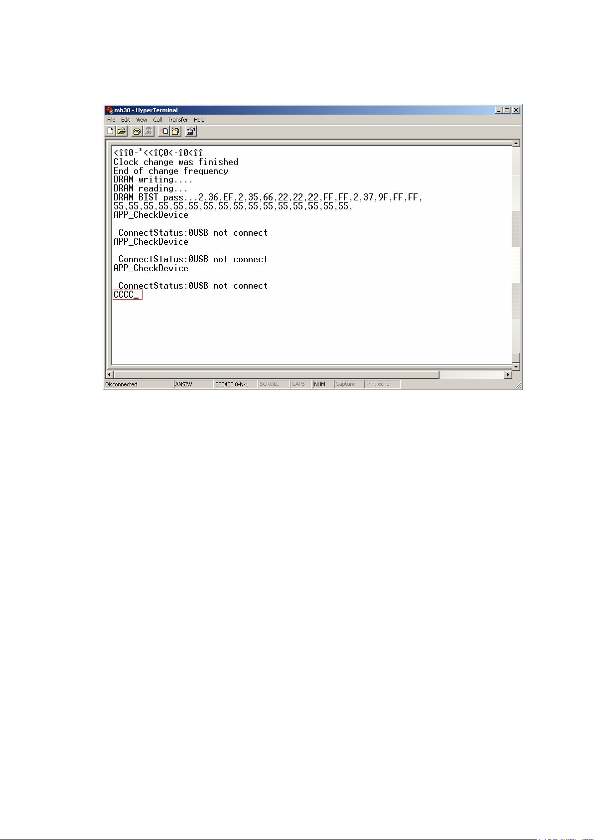
Figure 1. The Sample Output Before Sending The File
2. EEProm update
To Update eeprom content via uart scart,dsub9 or i2c with Mstar tool can used.
Serial connection settings are listed below:
- Bit per second: 9600
- Data bits: 8
- Parity: None
- Stop bits: 1
- Flow control: None
Programming menu item is choosed in the service menu and switch “HDCP Key Update
Mode” from off to on.
Page 9
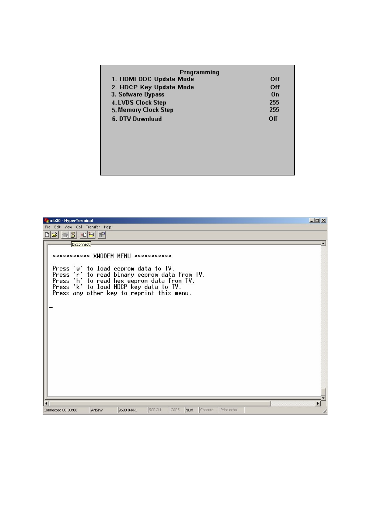
Figure 2. The Programming Service Menu
After then you must see Xmodem menu in the hyperterminal.To download hdcp key press
k or to download eeprom content press w.
Figure 3. Xmodem Menu
If the repeated “C” characters are seen you can transfer file content via select Transfer>Send File and choose “
Xmodem” protocol and click the “Send” button.
Page 10
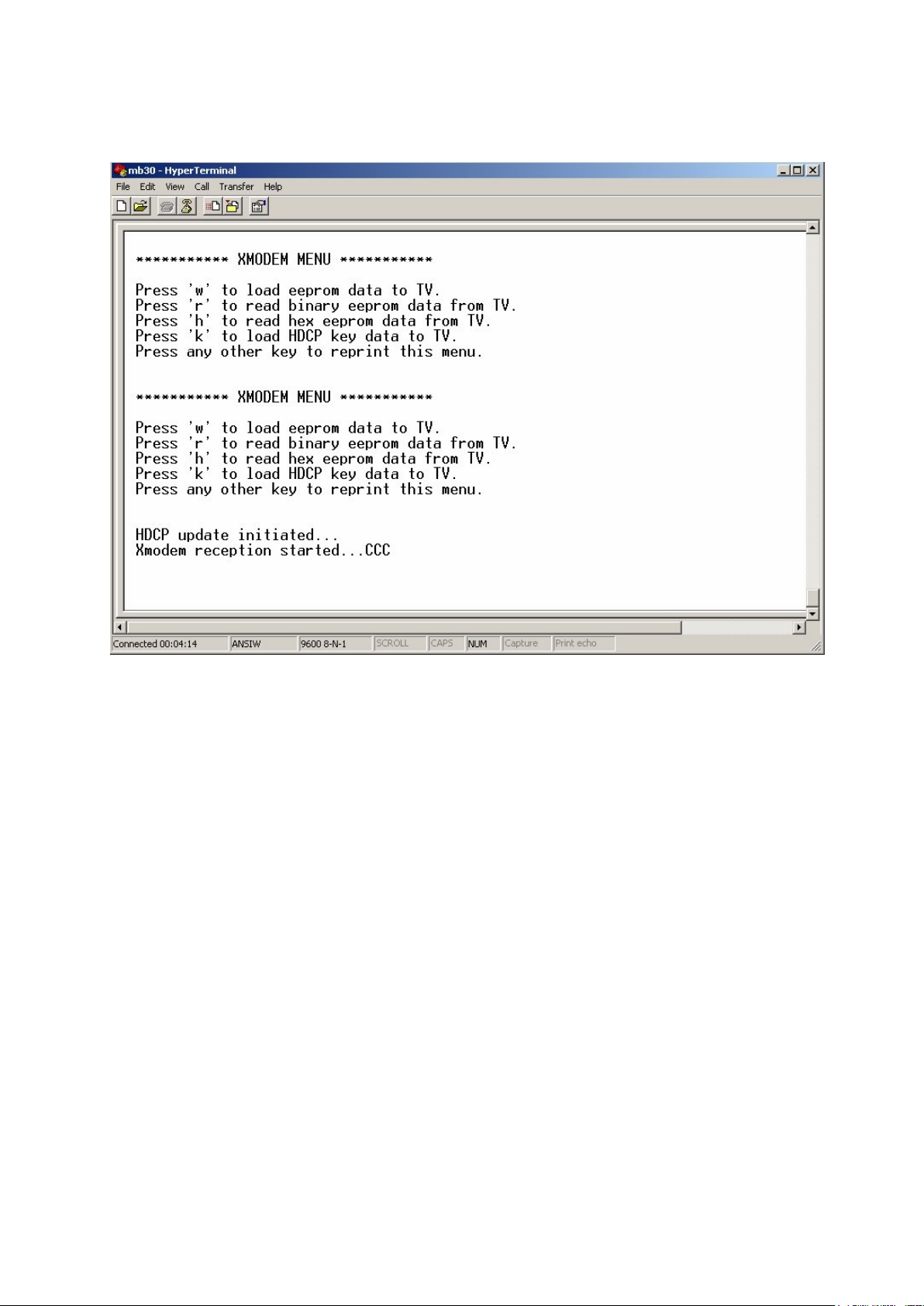
Figure 4. The Starting To Send
1.2. 17MB38 HDCP key upload procedure.
1) Turn on TV set.
2) Open a COM connection using fallowing parameters and select ISP COM Port No
Baud Rate: 9600 bps
Data Bits: 8
Stop Bits: 1
Parity: None
Flow Control: None
3) Enter service menu by pressing “1” “4” “6” 1” consecutively while main menu is
open
4) Select “9. Programming”
5) Select “HDMI HDCP Update Mode” yes.
6) On Hyper Terminal Window press “k”
7) Click on send file under Transfer Tab.
8) Select Xmodem and choose the HDCP key to be uploaded.
9) Press send button
10)Restart TV set
Page 11
1.3. 17MB38 Digital Software Update From SCART
Adjusting DTV Download Mode:
1. Power on the TV.
2. Exit the Stby Mode.
3. Enter the “Tv Menu”.
4. Enter “1461” for jumping to “Service Settings”.
5. Select “8. Programming” step.
6. Change “6. DTV Download” to “On”.
7. Switch to the Stby mode.
Adjusting HyperTerminal:
1. Connect the “MB38 SCART Interface” to SCART1 (bottom SCART plug).
2. Also connect the “MB38 SCART Interface” to PC.
3. Open “HyperTerminal”.
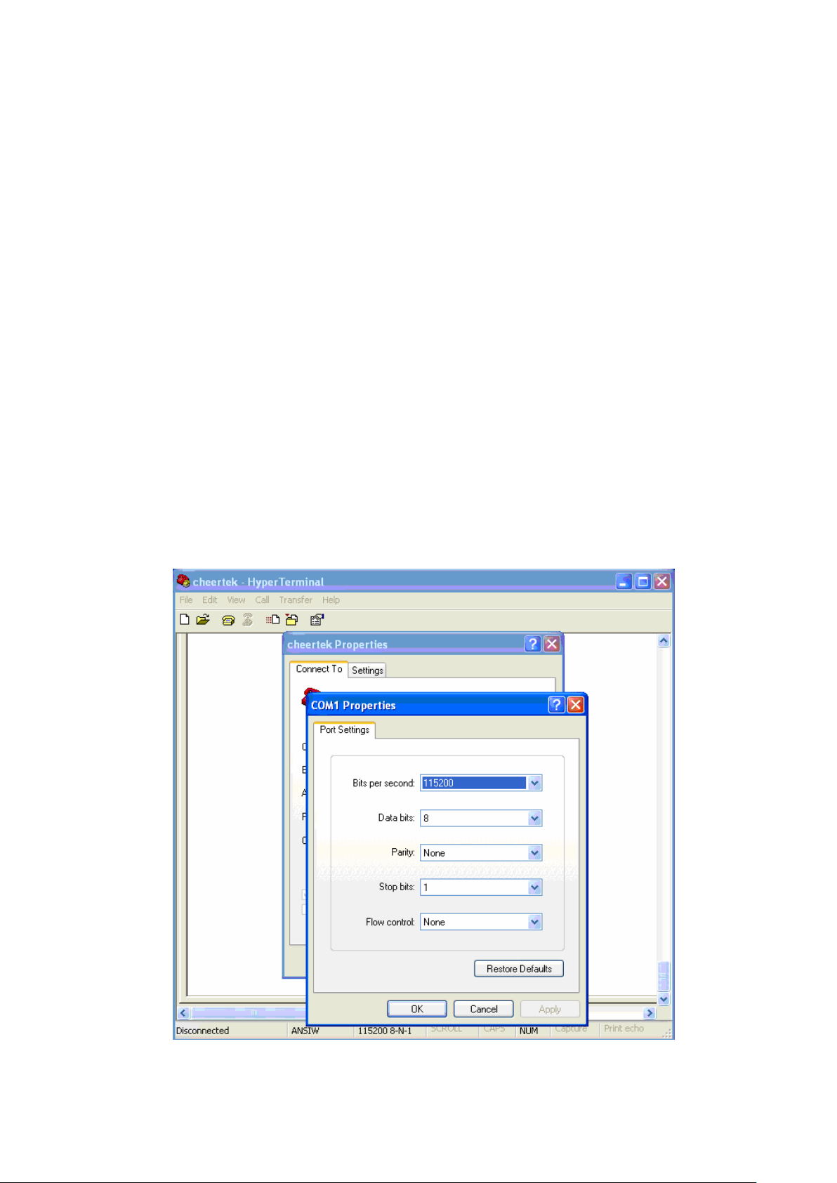
4. Determine the “COM” settings listed and showed below.
x Bit per second: 115200
x Data bits: 8
x Parity: None
x Stop bits: 1
x Flow control: None
COM Properties Window
Page 12
6. Click “OK”.
Software Updating Procedure
1. In the HyperTerminal Menu, click the “Connect” button.
2. Exit the Stby Mode.
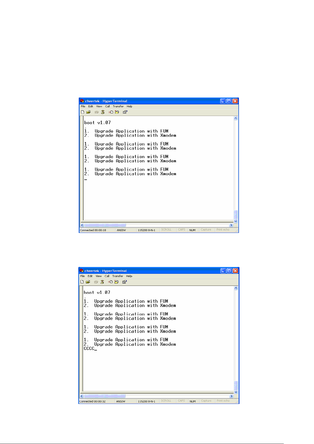
3. The “Space” button on the keyboard must be pressed, when the following window can
be seen.
Selection Window
4. Press the “2” button on the keyboard for choosing “2. Upgrade Application with
Xmodem”.
5. Repeating “C” characters are seen in the “HyperTerminal” menu.
Page 13
The Sample Output Before Sending The File
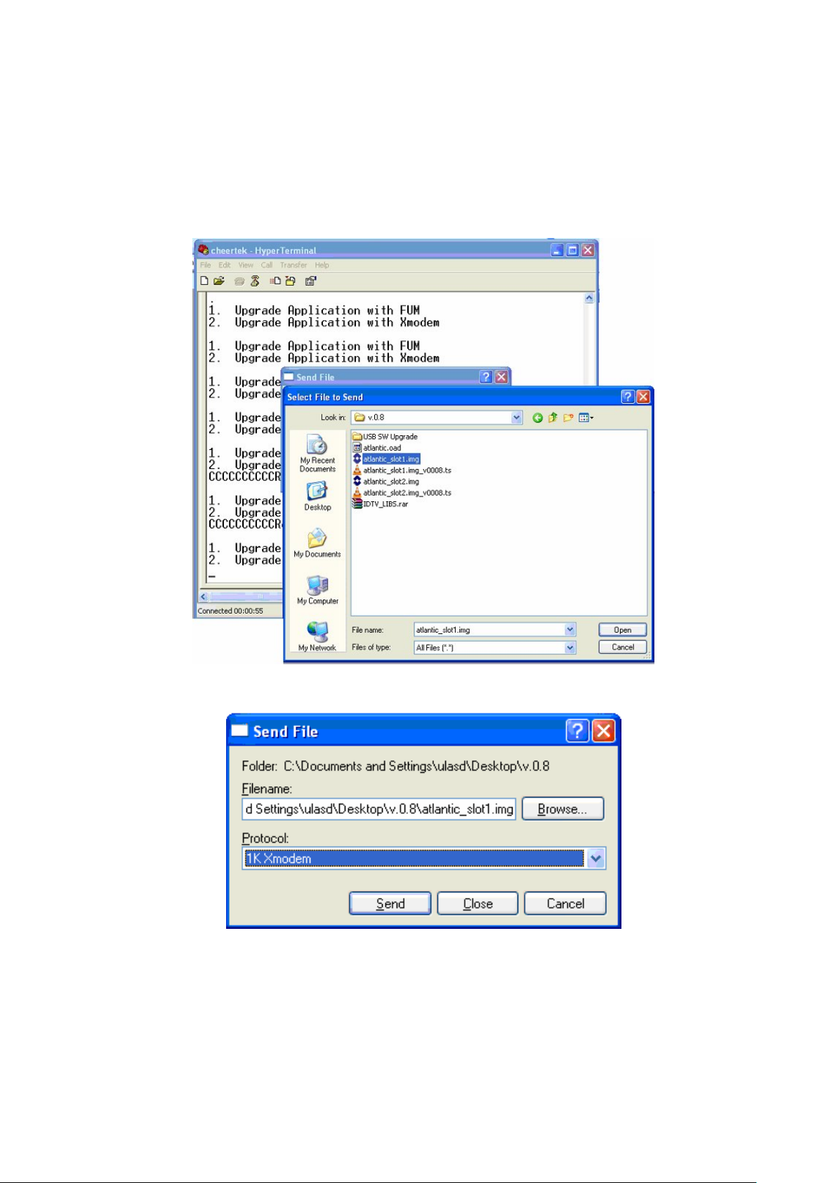
6. Click the “Send” button on the HyperTerminal
7. Select the “Filename
xxxx_slot1.img” using “Browse”.
8. Choose the “1K Xmodem” from “Protocol” option.
Selection of File
File and Protocol Selection Window
Note: In the Software updating Procedure section, when the first “C” character is seen,
the filename selection process must be finished before 10 seconds. If the process can not
be finished, the file sending operation will be cancelled. The following figure shows this
situation.
Page 14

Capture of Receving Data Failing
9. When sending the file the following window must be seen.
Capture of Sending Process
10. After the sending process the following HyperTerminal window must be seen.
Page 15

Capture of End of The Sending Process
11. For sending second program file, the Software Updating Procedure must be repeated
from the step
X. Select the “Filename xxxx_slot2.img” using “Browse”.
12. After sending the second program file, the Software Updating Procedure will be
succesful.
Note: After the File Sending Process,
1. Upgrade Application with FUM
2. Upgrade Application with Xmodem, options must be seen.
End of The Sending Process
Page 16

Checking Of The New Software
1. Turn off and on the TV.
2. Enter the “Setup” submenu in the “DTV Menu”.
3. Choose the “Configuration” option.
4. For controlling new software, check the “Receiver Upgrade” option.
1.4. 17MB38 Digital Software Update From USB
Software upgrade is possible via USB disk by folowing the steps below.
1. Copy the bin file, including higher version than the software loaded in flash, into the
USB flash memory root directory. This file should be named force_upgrade.bin .
2. Insert the USB disk.
3. Digital module performs version and CRC check. If version and CRC check is
successful, then a message prompt appears to notify user about new version. If the
user confirms loading of new version, upgrade.bin file is written into flash unused
slot.
4. Digital module disables the previous software in the flash and then a system reset
is performed.
5. After the reset, digital module starts with new software.
Page 17

3. TUNER
Samsung DTOS403LH122B tuner is used as the main part of the front-end. A horizontal
mounted and Digital Half-Nim tuner is used which covers 3 Bands(From 48MHz to
862MHz for COFDM, from 45.25MHz to 863.25MHz for CCIR CH). The tuning is available
through the digitally controlled I2C bus (PLL). Below you will find info about the tuner.
3.1. General description of DTOS403LH122B:
The Tuner covers 3 Bands(from 48MHz to 862MHz for COFDM, from 48.25MHz to
863.25MHz for CCIR CH). Band selection and Tuning are performed digitally via the I2C
bus.
3.2. Features of DTOS403LH122B:
x Digital Half-NIM tuner for COFDM
x Covers 3 Bands(From 48MHz to 862MHz for COFDM, from 48.25MHz to
863.25MHz for CCIR CH)
x Including IF AGC with SAW Filter
x Bandwidth Switching (7/8 MHz) possible
x DC/DC Converter built in for Tuning Voltage
x Internal(or External) RF AGC, Antenna Power Optional
3.3. Pinning
Page 18
3.4. AUDIO AMPLIFIER STAGE WITH MP7721General Description
17MB38 uses a 10W Class D Stereo Single Ended Audio Amplifer for audio. The MP7721
is a stereo 10W Class D Audio Amplif
integrated audio amplifiers which dramatically reduces solution size by integrating the
following:
x 180mSRZHU026)(7V
x Startup / Shutdown pop elimination
x Short circuit protection
x Mute / Standby
The MP7721 utilizes a single ended output structure capable of delivering 2 x 10W into
8
speakers. MPS Class D Audio Amplifiers exhibit the high fidelity of a Class A/B
amplifier at efficiencies greater than 90%. The circuit is based on the MPS’ proprietary
variable frequency topology that delivers low distortion, fast response time and operates
on a single power supply.
ier. It is one of MPS’ second generation of fully
3.5. Features
x 2 x 10W Output at VDD = 24V into a 8ORDG
x THD+N = 0.06% at 1W, 8
x 93% Efficiency at 10W
x Low Noise (190μV Typical)
x Switching Frequency Up to 1MHz
x 9.5V to 24V Operation from a Single Supply
x Integrated Startup and Shutdown Pop Elimination Circuit
x Thermal and Short Circuit Protection
x Integrated 180m6ZLWFKHV
x Mute/Standby Modes (Sleep)
x Thermally Enhanced 20-Pin TSSOP Package with Exposed Pad
Applications
x Surround Sound DVD Systems
x Televisions
x Flat Panel Monitors
x Multimedia Computers
x Home Stereo Systems
Page 19
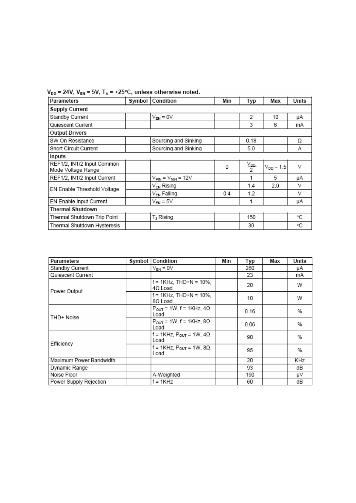
3.6. Absolute Ratings
3.6.1. Electrical Characteristics
3.6.2. Operating Specifications
Page 20
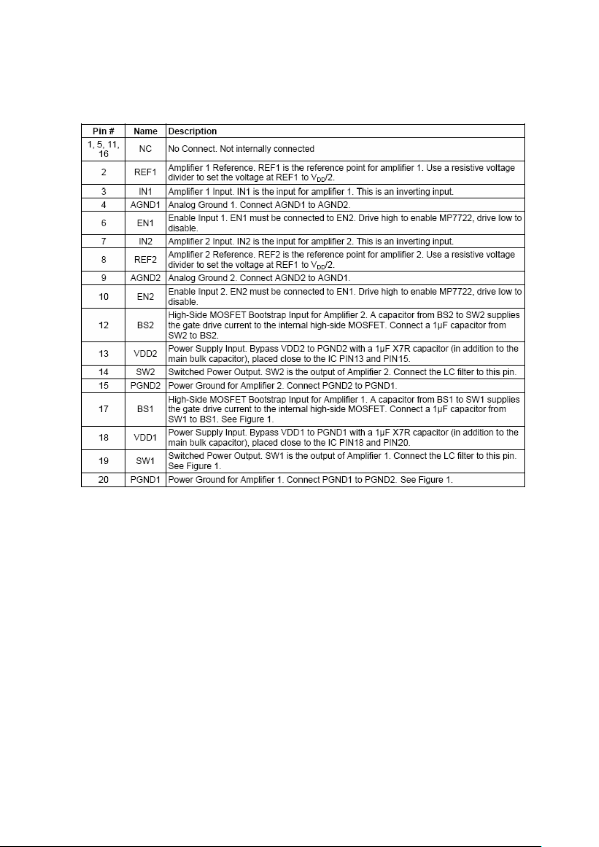
3.7. Pinning
4. POWER STAGE
The DC voltages required at various parts of the chassis and inverters are provided by a
main power supply unit. The power supply generates 24V, 12V, 5V, 3,3V and 5V, 3,3V
stand by mode DC voltages. Power stage which is on-chasis generates 1,26V stand by
voltage and 8V, 2.5V, 1,8V, 1,2V and 1V supplies for other different parts of the chassis.
Page 21
5. MICROCONTROLLER (MSTAR)
5.1. General Descripction
The MST6WB7GQ-3 is a high performance and fully integrated IC for multifunction LCD monitor/TV with resolutions up to full HD (1920x1080). It is configured
with an integrated triple-ADC/PLL, an integrated DVI/HDCP/HDMI receiver, a multistandard TV video and audio decoder, two video de-interlacers, two scaling engines, the
MStarACE-3 color engine, an on-screen display controller, an 8-bit MCU and a built-in
output panel interface. By use of external frame buffer, PIP/POP is provided for
multimedia applications. Furthermore, 3-D video decoding and processing are fulfilled
for high-quality TV applications. To further reduce system costs, the MST6WB7GQ-3
also integrates intelligent power management control capability for green-mode
requirements and spread-spectrum support for EMI management.
5.2. General Features
LCD TV controller with PIP/POP display functions
x Input supports up to UXGA & 1080P
x Panel supports up to full HD (1920x1080)
x TV decoder with 3-D comb filter
x Multi-standard TV sound demodulator and decoder
x 10-bit triple-ADC for TV and RGB/YPbPr
x 10-bit video data processing
x Integrated DVI/HDCP/HDMI compliant receiver
x High-quality dual scaling engines & dual 3-D video de-interlacers
x 3-D video noise reduction
x Full function PIP/PBP/POP
x MStarACE-3 picture/color processing engine
x Embedded On-Screen Display (OSD) controler engine
x Built-in MCU supports PWM & GPIO
x Built-in dual-link 8/10-bit LVDS transmitter
x 5-volt tolerant inputs
x Low EMI and power saving features
x 296-pin LQFP
Page 22

NTSC/PAL/SECAM Video Decoder
x Supports NTSC M, NTSC-J, NTSC-4.43, PAL (B,D,G,H,M,N,I,Nc), and SECAM
x Automatic TV standard detection
x Motion adaptive 3-D comb filter for NTSC/PAL
x 8 configurable CVBS & Y/C S-video inputs
x Supports Teletext level-1.5, WSS, VPS, Closed-caption, and V-chip
x Macrovision detection
x CVBS video output
Video IF for Multi-Standard Analog TV
x Digital low IF architecture
x Stepped-gain PGA with 26 dB tuning range and 1 dB tuning resolution
x Maximum IF analog gain of 37dB in addition to digital gain
x Programmable TOP to accommodate different tuner gain to optimize noise and
linearity performance
Multi-Standard TV Sound Decoder
x Supports BTSC/NICAM/A2/EIA-J demodulation and decoding
x FM stereo & SAP demodulation
x L/Rx4, mono, and SIF audio inputs
x L/Rx3 loudspeaker and line outputs
x Supports sub-woofer output
x Built-in audio output DAC’s
x Audio processing for loudspeaker channel, including volume, balance, mute, tone,
EQ, and virtual stereo/surround
x Optional advanced surround available (Dolby1, SRS2, BBE3… etc)
Digital Audio Interface
x I2S digital audio input & output
x S/PDIF digital audio input & output
x HDMI audio channel processing capability
x Programmable delay for audio/video synchronization
Analog RGB Compliant Input Ports
x Three analog ports support up to UXGA
x Supports HDTV RGB/YPbPr/YCbCr
x Supports Composite Sync and SOG (Sync-on-Green) separator
x Automatic color calibration
DVI/HDCP/HDMI Compliant Input Port
x Two HDMI input ports with built-in switch
x Supports TMDS clock up to 225MHz @ 1080P 60Hz with 12-bit deep-color
resolution
x Single link on-chip DVI 1.0 compliant receiver
x High-bandwidth Digital Content Protection(HDCP) 1.1 compliant receiver
Page 23
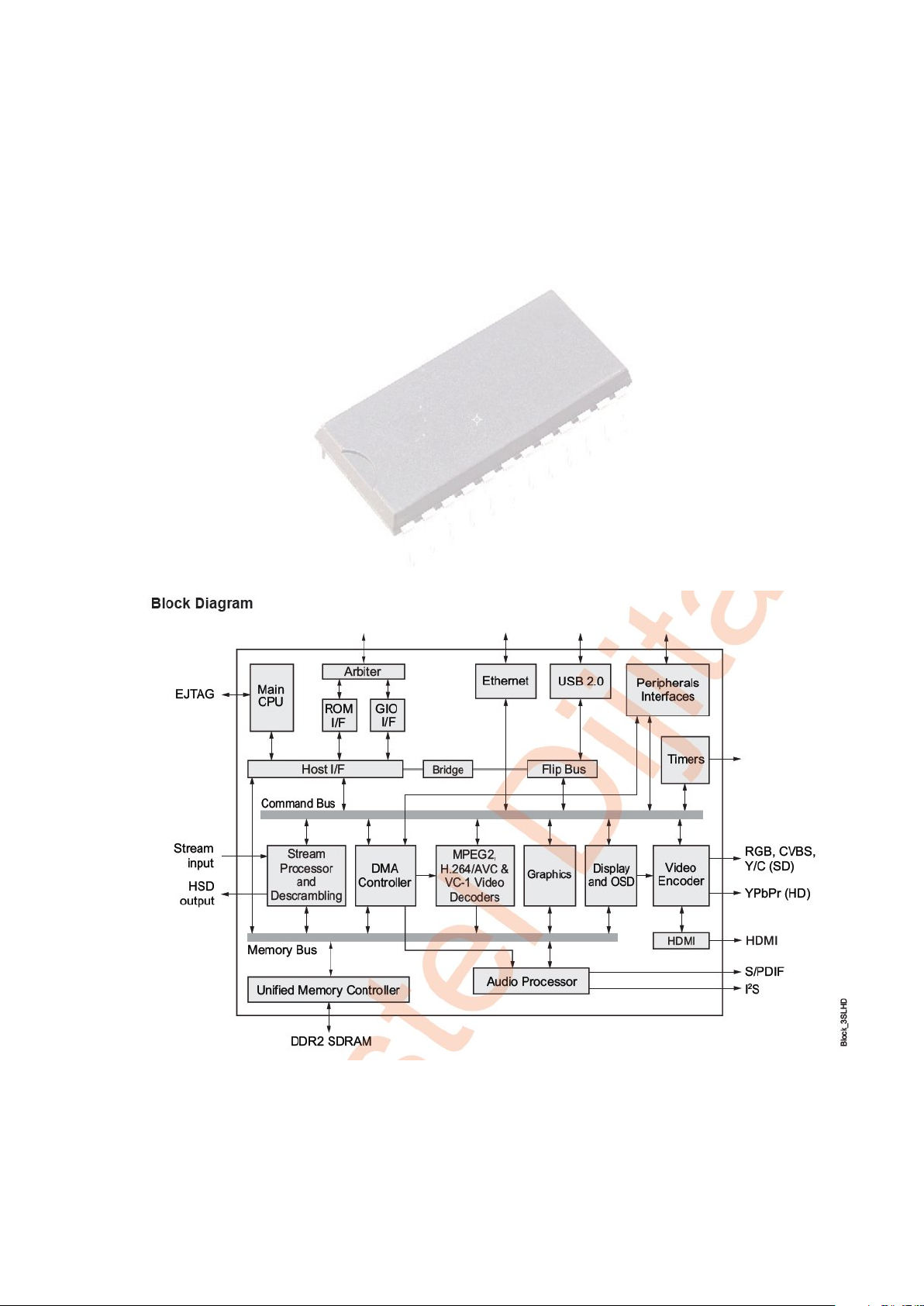
6. MPEG-2/MPEG-4 DVB Decoder – NEC EMMA3SL
6.1. General Description
The MC-10085/86/87/88 devices, EMMA3SL/HD, are part of the third generation of
multimedia processors based on NEC’s Enhanced MultiMedia Architecture (EMMA™). This
device provides nearly all the functionality required to realise a high performance and costeffective integrated digital TV.
NEC EMMA3SL integrates the functions of a TS de-multiplexer, a DMA controller, MPEG2,
H.264 (MPEG-4 part 10) and VC-1 video decoders, an audio processor, graphics and display
engines, a video encoder and DAC, and various interfaces to support peripheral modules.
The device has been designed with a memory interface using glueless logic which supports
DDR2 SDRAM. The MC-10085/86/87/88 incorporate a processor, two main buses and a
peripherals bus. The processor is a MIPS32 24KEc core and can access all modules within the
device.
Figure 6.1 Block Diagram of NEC EMMA3SL
Page 24

6.2 Features
Main Processor
- High Performance MIPS32 24KEc CPU core
- 32 bit RISC MIPS architecture
- Supports the MIPS16, MIPS-I, MIPS-II and MIPS-III instruction sets
- 16 KByte instruction cache, 16 KByte data cache
- 2 way cache accessing
- EJTAG debug support
Unified Memory Interface
- Supports 16/32 bit bus width DDR2-SDRAM
- Unified CPU/MPEG/Graphics memory
- Supports data rates up to 655 MHz
- Supports 256 ~ 2048 Mbit total memory
ROM/GIO Interface
- Total address area 64Mbyte for ROM
- Supports normal, page and flash ROM
- Supports NOR and NAND flash ROM
- 4 chip select signals for both ROM and GIO
- 16 MByte total address area for GIO
- Up to 4 Gbit NAND
- PCMCIA support
Stream Processor
- Supports MPEG2-TS (DVB)
- Four dedicated transport stream input ports – two serial and two parallel
- One further channel for input of transport streams via a CPU-controlled register
- Total maximum input bit rate of 108 Mbits/sec
- 36 PID filters
• 1 Video PIDs
• 2 Audio PIDs
• 1 PCR PIDs
• 32 general PIDs
- 32 section filters (8-Byte/16-Byte depth) in four configurable banks
- High Speed Data output port for interfacing to external devices
- DVB descrambling support
Descrambler
- Supports DES, 3DES and AES
DMA
- Supports DMA transfer between internal units and DDR2-SDRAM
Page 25

MPEG video decoder
- MPEG-2: MP@ML, MP@HL
- MPEG-4: ASP@L5 w/o QMC, GMC
- H.264/AVC: HP@L4.0, MP@L4.0, 3.2
- VC-1: AP@L3, AP@L2
- DivX Home Theatre Profile 3.11, 4.x, 5.x, 6.x (MC-10085/86 only)
Audio Processor
- MPEG-1 and -2, layer 1 and 2
- MPEG-4 HE-AAC V1L1, L2, V2 L2/L4
- Supports MPEG2 half-rate streams
- Dolby Digital Plus
- Support for downmixing Dolby Digital/Dolby Digital Plus to 2 ch PCM
- Dolby Digital Plus to Dolby Digital transcode
- DualMono L+R audio output
- SPDIF with IEC60958 output (Dolby Digital can be passed through to SPDIF)
- Sample rate conversion, test-tone and mixer
- Suports Audio Description
- 5.1 ch output, MP3 and WMA optional
Graphics engine
- 2-D and 1-D image data transfer
- Colour space conversion: RGB32 to YCbCr
- Colour expansion
- X-Y scaler
- Porter-Duff alpha compositing support
Display
- 6 graphics planes: background colour, live video for SD and HD, still picture
and two OSD planes
- 256-level alpha blending between all planes
- Real time scaler for live video and still planes supporting independent horizontal and vertical
scale factors between 8 and 1/4
- Anti-flicker filtering for OSD
- Independently blended output for VCR
Video Encoder
- 6 DACs for analog video output:
• 3 DACs for SD output: RGB, CVBS or Y/C
• 3 DACS for HD ouput: YPbPr
- PAL, SECAM and NTSC formats
- VBI insertion for Closed-Caption, Teletext, Video-ID, WSS, VPS and CGMS
- Support for Macrovision analog video copy protection (7.1L1 and AGC1.2) (MC-10086/88
only)
Page 26

HDMI Transmitter
- Industry-standard compliance:
• HDMI 1.3 with x.v. Colour
• DVI 1.0
• EIA/CEA-861D
• HDCP 1.1
- Integrated HDMI TMDS core running at 165 MHz (support up to 1.65 Gbps)
Peripherals support
- Two asynchronous 16550 UARTs
- One other UART
- Clocked Serial Interface
- Two ISO 7816-3 compliant Smart Card interfaces
- Two I2C compatible interfaces
- Two infrared receiver interfaces and one transmitter
- Programmable Pin Port shared with other peripherals (152 channels maximum)
Timers
- Two timers supporting input capture and output compare
- Two system timers, a real time clock and a watchdog timer
USB 2.0
- USB 2.0 high speed host controller/PHY interface – 1 channel
Ethernet
- 100BT Ethernet controller with integrated MAC and /RMII interface for external PHY
- Supports 10/100 Mbps and full duplex operation
Package
- 596-pin, 1 mm pitch PBGA (Plastic Ball Grid Array)
Page 27

6.3 Absolute Maximum Ratings
Page 28
7 SIL9185 3:1 HDMI 1.3 Switch
7.1 General Description
The SiI9185A is the first generation of TMDS switch device supporting Revision 1.3 of the
HDMI Specification (HDMI Consortium; June 2006). With three HDMI inputs and a single
output, the SiI9185A provides a low-cost method of adding additional HDMI ports to the
latest Digital TVs. New DTVs can easily connect to the many HDMI sources coming on
the market, including DVDs, STB, game consoles, PCs, camcorders, and digital still
cameras. The SiI9185A is a fully HDMI compliant device providing a simple, lowcost
method of retransmitting protected digital audio and video, giving end-users a truly alldigital experience. Built-in backward compatibility with DVI 1.0 allows HDMI systems to
connect to any DVI 1.0 source. The SiI9185A provides additional integrated features to
help lower system cost and provide enhanced features to the end consumer. To lower
system cost, the SiI9185A provides a complete solution for switching sink-side HDMI
signals. This includes DDC switching, individual HPD control, and 5V sense. The addition
of these features eliminates additional external components, helping to lower cost. For
source-side applications, the SiI9185A DDC switching can be bypassed with an external
4-channel I2C-bus switch(e.g., Texas Instruments PCA95445) to allow clock
stretching.
7.2 Features
x Three-input, single-output HDMI switcher
x Integrated TMDS® receiver and transmitt cores capable of receiving and
transmitting 2.25 Gbps:
x Support 60 Hz, 12-bit or 720p/1080i, 120 Hz, 12-bit
x Builcable support even at deep-color resolutions
x Pre-emphasi
x DVI 1.0, HDCP 1.1 and HDM compliant receiver and transmitter
x Uses HDMI-compliant TMDS core recovery and retransmission, unlike TMDS
switches, which use high-spee analog switches and degrade TMDS signals
x Built-in Cons support:
x HDM lowers cost for adding CEC support to DTV
x Integra requirements on system microcontrolle speeds design
Page 29
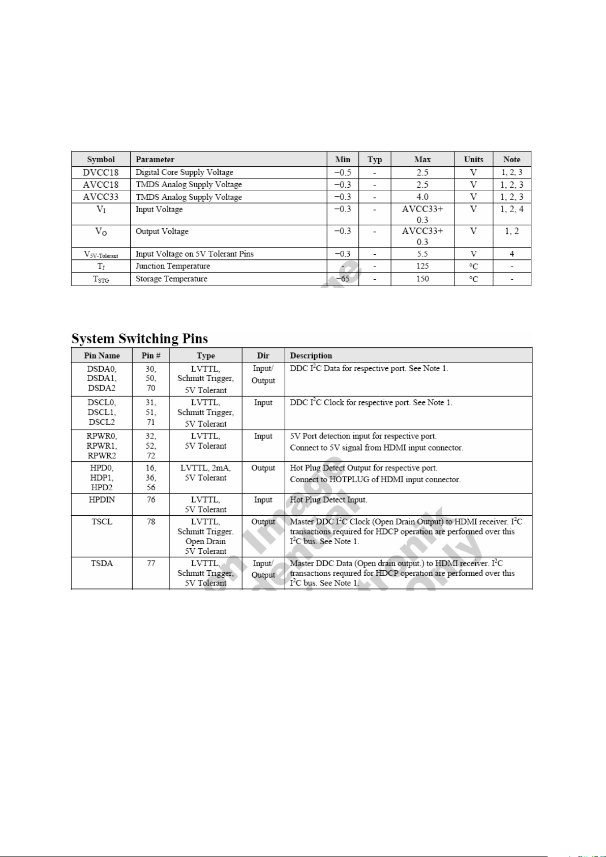
7.3 Absolute Maximum Ratings
7.4 Pinning
Page 30

Page 31

8 DVB-T/T2 DEMODULATOR – SONY CXD2820R
8.1 General Description
The Sony CXD2820R is a combined DVB-T2, DVB-T and DVB-C demodulator that conforms to
the ETSI EN 302-755 (second generation Terrestrial) ETSI EN 300-744 (Terrestrial) and ETSI EN
300-429 (Cable) standards.
The CXD2820R is a DVB-T2 demodulator offering class-leading performance, optimised BOM
requiring no external memory and low processor overhead. It includes a highly integrated dualcore DVB-T and DVB-C demodulator which complies with all relevant European performance
standards.
Figure 8.1 Block Diagram of SONY CXD2820R
Applications
• Set Top Boxes
• IDTV with Digital only or Hybrid Tuner Support
• PC TV
• PVRs and recordable DVD players
• Test equipment
Page 32

8.2 Features
General Features
• Single, 41MHz crystal (can be shared with CXD2813R analogue demod IC)
• High performance differential signal ADC
• RF power level monitor ADC
• Low IF and high IF (36MHz) mode input
• Fast 400kHz I2C compatible bus interface
• Quiet I2C interface for dedicated tuner control
• Automatic IF AGC and optional programmable RF AGC/GPIO functions
• Configurable parallel and serial MPEG-2 TS outputs with smoothing buffer
• 3.3V, 2.5V, 1.2V supplies
• Temperature range -20°C to +85°C
• 64 pin exposed-pad LQFP 10mm x 10mm package
• Supplied with full reference design, including software driver, PCB schematic/layouts, GUI and
documentation
Features DVB-T
• Complies with all European standards for static and portable equipment including NorDig
Unified 2.0, DTG 6.0, Ebook
• Smart Auto Acquisition controller with fast 2k/8k acquisition, low processor overhead and reacquisition mode
• Acquisition range ±600kHz
• Automatic spectral inversion
• Enhanced in the following areas
• SFN perf. with pre/post-cursive echoes inside/outside guard
• Impulse noise cancellation algorithm compliant with DTG & Ebook
• ACI protection and performance with CCI
• Advanced channel corrector for low multipath loss and enhanced Doppler performance
• Access to channel echo profile, channel and individual carrier SNR, constellation and TPS data
(inc cell identification) via I2C
Features DVB-T2
• Supports all DVB-T2 modes, including
• Single and multiple-PLPs
• SISO and MISO transmission
• Simple API
• Fully-automatic acquisition
• Fully-automatic L1-signalling decoding
• Automatic guard-interval detection
• Automatically-calculated constant-rate TS output (using L1 signalling and ISSY)
• Acquisition range ±600kHz
• Stream processor for automatic common- and data-PLP combination
• Null-packet insertion
• Access to channel echo profile and constellation via I2C
Page 33

8.3 Absolute Maximum Rating
Page 34

8.4 Pinning
Page 35

Page 36

Page 37

9 WINBOND W9425G6EH DDR SDRAM 128M
9.1 General Description
W9425G6EH is a CMOS Double Data Rate synchronous dynamic random access
memory (DDR SDRAM), organized as 4,194,304 words u 4 banks u 16 bits. W9425G6EH
delivers a data bandwidth of up to 500M words per second (-4). To fully comply with the
personal computer industrial standard, W9425G6EH is sorted into the following speed
grades: -4, -5, -5I, -6 and -6I. The -4 is compliant to the DDR500/CL3 and CL4
specification. The -5/-5I is compliant to the DDR400/CL3 specification (the -5I grade
which is guaranteed to support -40°C ~ 85°C). The -6/-6I is compliant to the
DDR333/CL2.5 specification (the -6I grade which is guaranteed to support -40°C ~ 85°C).
All Input reference to the positive edge of CLK (except for DQ, DM and CKE). The timing
reference point for the differential clock is when the CLK and CLK signals cross during a
transition. Write and Read data are synchronized with the both edges of DQS (Data
Strobe). By having a programmable Mode Register, the system can change burst length,
latency cycle, interleave or sequential burst to maximize its performance.
9.2 Features
- 2.5V r0.2V Power Supply for DDR333/400
- 2.6V r0.1V Power Supply for DDR500
- Up to 250 MHz Clock Frequency
- Double Data Rate architecture; two data transfers per clock cycle
- Differential clock inputs (CLK and CLK )
- DQS is edge-aligned with data for Read; center-aligned with data for Write
- CAS Latency: 2, 2.5, 3 and 4
- Burst Length: 2, 4 and 8
- Auto Refresh and Self Refresh
- Precharged Power Down and Active Power Down
- Write Data Mask
- Write Latency = 1
- 7.8μS refresh interval (8K/64 mS refresh)
- Maximum burst refresh cycle: 8
- Interface: SSTL_2
Page 38

9.3 Absolute Maximum Ratings
9.4 Pinning
Page 39

Page 40

10 ELPIDA EDE5116AJBG DDR SDRAM
10.1 General Description
There are 2 Elpida EDE5116AJBG (32M x 16 bits) DDR2 SDRAM used for NEC
EMMA3SL microcontroller functions and MPEG2/MPEG4 decoding functions. Data pins
are connected parallel and the address selection is varied for different memory access
locations.
10.2 Features
• Double-data-rate architecture; two data transfers per clock cycle
• The high-speed data transfer is realized by the 4 bits prefetch pipelined architecture
• Bi-directional differential data strobe (DQS and /DQS) is transmitted/received with data
for capturing data at the receiver
• DQS is edge-aligned with data for READs; centeraligned with data for WRITEs
• Differential clock inputs (CK and /CK)
• DLL aligns DQ and DQS transitions with CK transitions
• Commands entered on each positive CK edge; data and data mask referenced to both
edges of DQS
• Data mask (DM) for write data
• Posted /CAS by programmable additive latency for better command and data bus
efficiency
• Off-Chip-Driver Impedance Adjustment and On-Die-Termination for better signal quality
• Programmable RDQS, /RDQS output for making × 8 organization compatible to × 4
organization
• /DQS, (/RDQS) can be disabled for single-ended Data Strobe operation
11.3 Absolute Maximum Ratings
Page 41

11.4 Pinning
Page 42

11 Ethernet PHY - KSZ8041RNL
11.1 General Description
The KSZ8041RNL is a single supply 10Base-T/100Base-TX Physical Layer Transceiver
with RMII support. It uses a 25MHz crystal for its reference clock and outputs a 50MHz
RMII reference clock to the MAC.
The KSZ8041RNL employs a unique mixed signal design to extend cable reach while
reducing power consumption. HP Auto MDI/MDI-X provides the most robust solution for
eliminating the need to differentiate between crossover and straight-through cables.
Page 43

11.2 Features
• Single-chip 10Base-T/100Base-TX physical layer solution
• Fully compliant to IEEE 802.3u Standard
• Low power CMOS design, power consumption of <180mW
• HP auto MDI/MDI-X for reliable detection and correction for straight-through and crossover
cables with disable and enable option
• Robust operation over standard cables
• Power down and power saving modes
• RMII interface support with 50MHz reference clock output to MAC
• MIIM (MDC/MDIO) management bus to 6.25MHz for rapid PHY register configuration
• Interrupt pin option
• Programmable LED outputs for link, activity and speed
• ESD rating (6kV)
• Single power supply (3.3V)
• Built-in 1.8V regulator for core
• Available in 32-pin (5mm x 5mm) MLF® package
11.3 Absolute Maximum Ratings
Page 44

11.4 Pinning
Page 45

Page 46

12 SAW FILTER
12.1 IF Filter for Audio Applications – Epcos K9656M
12.1.1 Standart:
x B/G
x D/K
x I
x L/L’
12.1.2 Features:
x TV IF audio filter with two channels
x Channel 1 (L’) with one pass band for sound carriers at 40,40 MHz (L’) and 39,75
MHz (L’- NICAM)
x Channel 2 (B/G,D/K,L,I) with one pass band for sound carriers between 32,35 MHz
and 33,40 MHz
12.1.3 Pin configuration:
1 Input
2 Switching input
3 Chip carrier - ground
4 Output
5 Output
12.1.4 Frequency response:
Page 47

Page 48

12.2 IF Filter for Video Applications – Epcos K3958M
12.2.1 Standart:
x B/G
x D/K
x I
x L/L’
12.2.2 Features:
x TV IF filter with Nyquist slopes at 33.90 MHz and 38.90 MHz
x Constant group delay
Pin configuration:
1 Input
2 Input - ground
3 Chip - carrier ground
4 Output
5 Output
12.2.3 Frequency response:
Page 49

13 32K Smart Serial EEPROM – 24C32
13.1 General Description
The Microchip Technology Inc. 24C32 is a 4K x 8 (32K bit) Serial Electrically Erasable
PROM. This device has been developed for advanced, low power applications such as
personal communications or data acquisition. The 24C32 features an input cache for fast
write loads with a capacity of eight 8-byte pages, or 64 bytes. It also features a fixed 4Kbit block of ultra-high endurance memory for data that changes frequently. The 24C32 is
capable of both random and sequential reads up to the 32K boundary. Functional address
lines allow up to eight 24C32 devices on the same bus, for up to 256K bits address
space. Advanced CMOS technology makes this device ideal for low-power non-volatile
code and data applications. The 24C32 is available in the standard 8-pin plastic DIP and
8-pin surface mount SOIC package.
13.2 Features
x Voltage operating range: 4.5V to 5.5V
x Peak write current 3 mA at 5.5V
x Maximum read current 150 μA at 5.5V
x Standby current 1 μA typical
x Industry standard two-wire bus protocol, I2C compatible
x Including 100 kHz and 400 kHz modes
x Self-timed write cycle (including auto-erase)
x Power on/off data protection circuitry
x Endurance: 10,000,000 Erase/Write cycles guaranteed for High Endurance Block,
1,000,000 E/W cycles guaranteed for Standard Endurance Block
Page 50

x 8 byte page, or byte modes available
x 1 page x 8 line input cache (64 bytes) for fast write loads
x Schmitt trigger, filtered inputs for noise suppression
x Output slope control to eliminate ground bounce
x 2 ms typical write cycle time, byte or page
x Up to 8 chips may be connected to the same bus for up to 256K bits total memory
x Electrostatic discharge protection > 4000V
x Data retention > 200 years
x 8-pin PDIP/SOIC packages
x Temperature ranges: Commercial (C): 0°C to +70°C, Industrial (I): -40°C to +85°C
11.3 Absolute Maximum Ratings and Electrical Characteristics
Page 51

11.4 Pinning
Page 52

14 512K CMOS Serial Flash – MX25L512
14.1 General Description
The MX25L512 is a CMOS 524,288 bit serial Flash memory, which is configured as
65,536 x 8 internally. The MX25L512 feature a serial peripheral interface and software
protocol allowing operation on a simple 3-wire bus. The three bus signals are a clock
input (SCLK), a serial data input (SI), and a serial data output (SO). SPI access to the
device is enabled by CS# input. The MX25L512 provide sequential read operation on
whole chip. After program/erase command is issued, auto program/ erase algorithms
which program/ erase and verify the specified page or sector/block locations will be
executed. Program command is executed on page (256 bytes) basis, and erase
command is executes on chip or sector (4K-bytes). To provide user with ease of interface,
a status register is included to indicate the status of the chip. The status read
command can be issued to detect completion status of a program or erase operation via
WIP bit. When the device is not in operation and CS# is high, it is put in standby mode
and draws less than 10uA DC current. The MX25L512 utilize MXIC's proprietary memory
cell, which reliably stores memory contents even after 100,000 program and erase cycles.
14.2 Features
GENERAL
x Serial Peripheral Interface (SPI) compatible -- Mode 0 and Mode 3
x 524,288 x 1 bit structure
x 16 Equal Sectors with 4K byte each
x Any Sector can be erased individually
x Single Power Supply Operation
x 2.7 to 3.6 volt for read, erase, and program operations
x Latch-up protected to 100mA from -1V to Vcc +1V
x Low Vcc write inhibit is from 1.5V to 2.5V
PERFORMANCE
x High Performance
x Fast access time: 85MHz serial clock (15pF + 1TTL Load) and 66MHz serial clock
(30pF + 1TTL Load)
x Fast program time: 1.4ms(typ.) and 5ms(max.)/page (256-byte per page)
x Fast erase time: 60ms(typ.) and 120ms(max.)/sector (4K-byte per sector) ; 1s(typ.)
and 2s(max.)/chip(512Kb)
x Low Power Consumption
x Low active read current: 12mA(max.) at 85MHz, 8mA(max.) at 66MHz and
4mA(max.) at 33MHz
x Low active programming current: 15mA (max.)
x Low active erase current: 15mA (max.)
x Low standby current: 10uA (max.)
x Deep power-down mode 1uA (typical)
x Minimum 100,000 erase/program cycles
SOFTWARE FEATURES
Page 53

x Input Data Format
x 1-byte Command code
x Block Lock protection
x The BP0~BP1 status bit defines the size of the area to be software protected
against Program and Erase instructions.
x Auto Erase and Auto Program Algorithm
x Automatically erases and verifies data at selected sector
x Automatically programs and verifies data at selected page by an internal algorithm
that automatically times the program pulse widths (Any page to be programed
should have page in the erased state first)
x Status Register Feature
x Electronic Identification
x JEDEC 2-byte Device ID
x RES command, 1-byte Device ID
HARDWARE FEATURES
x SCLK Input
x Serial clock input
x SI Input
x Serial Data Input
x SO Output
x Serial Data Output
x WP# pin
x Hardware write protection
x HOLD# pin pause the chip without diselecting the chip
x PACKAGE
x 8-pin SOP (150mil)
x All Pb-free devices are RoHS Compliant
11.3 Absolute Maximum Ratings
Page 54

Page 55

15IC DESCRIPTIONS
15.1 LM1117
15.1.1 General Description
The LM1117 is a series of low dropout voltage regulators with a dropout of 1.2V at 800mA
of load current. It has the same pin-out as National Semiconductor’s industry standard
LM317. The LM1117 is available in an adjustable version, which can set the output
voltage from 1.25V to 13.8V with only two external resistors. In addition, it is also
available in five fixed voltages, 1.8V, 2.5V, 2.85V, 3.3V, and 5V. The LM1117 offers
current limiting and thermal shutdown. Its circuit includes a zener trimmed bandgap
reference to as-sure output voltage accuracy to within ±1%. The LM1117 series is
available in SOT- 223, TO-220, and TO-252 Dtantalum capacitor is required at the output to improve the transient response and
stability.
15.1.2 Features
x Available in 1.8V, 2.5V, 2.85V, 3.3V, 5V, and Adjustable Versions
x Space Saving SOT-223 Package
x Current Limiting and Thermal Protection
x Output Current 800mA
x Line Regulation 0.2% (Max)
x Load Regulation 0.4% (Max)
x Temperature Range
x LM1117 0°C to 125°C
x LM1117I -40°C to 125°C
3$. SDFNDJHV $ PLQLPXP RI ȝ)
15.1.3 Applications
x 2.85V Model for SCSI-2 Active Termination
x Post Regulator for Switching DC/DC Converter
x High Efficiency Linear Regulators 15
x 32” TFT TV Service Manual 10/01/2005
x Battery Charger
x Battery Powered Instrumentation
15.1.4 Absolute Maximum Ratings
Page 56

15.1.5 Pinning
15.2 74HCT4053
15.2.1 General Description
The 74HC4053; 74HCT4053 is a high-speed Si-gate CMOS device and is pin compatible
with the HEF4053B. It is specified in compliance with JEDEC standard no. 7A. The
74HC4053; 74HCT4053 is triple 2-channel analog multiplexer/demultiplexer with a
common enable input (E). Each multiplexer/demultiplexer has two independent
inputs/outputs (nY0 and nY1), a common input/output (nZ) and three digital select inputs
(Sn). With E LOW, one of the two switches is selected (low-impedance ON-state) by S1 to
S3. With E HIGH, all switches are in the high-impedance OFF-state, independent of S1 to
S3. VCC and GND are the supply voltage pins for the digital control inputs (S1 to S3 and
E). The VCC to GND ranges are 2.0 V to 10.0 V for 74HC4053 and 4.5 V to 5.5 V for
74HCT4053. The analog inputs/outputs (nY0 and nY1, and nZ) can swing between VCC
as a positive limit and VEE as a negative limit. VCC - VEE may not exceed 10.0 V.
For operation as a digital multiplexer/demultiplexer, VEE is connected to GND (typically
ground).
15.2.2 Features
x Low ON resistance:
x 80 W (typical) at VCC - VEE = 4.5 V
x 70 W (typical) at VCC - VEE = 6.0 V
x 60 W (typical) at VCC - VEE = 9.0 V
x Logic level translation:
x To enable 5 V logic to communicate with ±5 V analog signals
x Typical ‘break before make’ built in
x Complies with JEDEC standard no. 7A
x ESD protection: HBM EIA/JESD22-A114-C exceeds 2000 V, MM EIA/JESD22-
A115-A exceeds 200 V
x Multiple package options
x Specified from -40 °C to +85 °C and from -40 °C to +125 °C
15.2.3 Applications
x Analog multiplexing and demultiplexing
x Digital multiplexing and demultiplexing
x Signal gating
Page 57

15.2.4 Absolute Maximum Ratings
15.2.5 Pinning
Page 58

15.3 NUP4004M5
15.3.1 General Description
This 5-Pin bi-directional transient suppressor array is designed for applications requiring
transient overvoltage protection capability. It is intended for use in transient voltage and
ESD sensitive equipment such as computers, printers, cell phones, medical equipment,
and other applications. Its integrated design provides bi-directional protection for four
separate lines using a single TSOP-5 package. This device is ideal for situations where
board space is a premium.
15.3.2 Features
x Bi-directional Protection for Four Lines in a Single TSOP-5 Package
x Low Leakage Current
x Low Capacitance
x Provides ESD Protection for JEDEC Standards JESD22
x Machine Model = Class C
x Human Body Model = Class 3B
x Provides ESD Protection for IEC 61000-4-2, 15 kV (Air), 8 kV (Contact)
x This is a Pb-Free Device
15.3.3 Absolute Maximum Ratings
Page 59

15.3.4 Pinning
15.4 FDN336P
15.4.1 General Description
The ST24LC21 is a 1K bit electrically erasable programmable memory (EEPROM),
organized by 8 bits.This device can operate in two modes: Transmit Only mode and I2C
bidirectional mode. When powered, the device is in Transmit Only mode with EEPROM
data clocked out from the rising edge of the signal applied on VCLK. The device will
switch to the I2C bidirectional mode upon the falling edge of the signal applied on SCL
pin. The ST24LC21 cannot switch from the I2C bidirectional mode to the Transmit Only
mode (except when the power supply is removed). The device operates with a power
supply value as low as 2.5V. Both Plastic Dual-in-Line and Plastic Small Outline
packages are available.
15.4.2 Features
x 1 MILLION ERASE/WRITE CYCLES
x 40 YEARS DATA RETENTION
x 2.5V to 5.5V SINGLE SUPPLY VOLTAGE
x 400k Hz COMPATIBILITY OVER the FULL RANGE of SUPPLY VOLTAGE
x TWO WIRE SERIAL INTERFACE I2C BUS COMPATIBLE
x PAGE WRITE (up to 8 BYTES)
x BYTE, RANDOM and SEQUENTIAL READ MODES
x SELF TIMED PROGRAMMING CYCLE
x AUTOMATIC ADDRESS INCREMENTING
x ENHANCED ESD/LATCH UP PERFORMANCES
Page 60

15.4.3 Absolute Maximum Ratings
15.4.4 Pinning
15.5 TL062 -
15.5.1 General Description
Low-power JFET-input operational amplifier
15.5.2 Features
x Very Low Power Consumption
x Typical Supply Current . . . 200 μA (Per Amplifier)
x Wide Common-Mode and Differential Voltage Ranges
x Low Input Bias and Offset Currents
x Common-Mode Input Voltage Range Includes VCC+
x Output Short-Circuit Protection
x High Input Impedance . . . JFET-Input Stage
x Internal Frequency Compensation
x Latch-Up-Free Operation
x High Slew Rate . . . 3.5 V/μs Typ
Page 61

15.5.3 Absolute Maximum Ratings
15.5.4 Pinning
15.6 PI5V330
15.6.1 General Description
Pericom Semiconductor.s PI5V series of mixed signal video circuits are produced in the
Company.s advanced CMOS low-power technology, achieving industry leading
performance. The PI5V330 is a true bidirectional Quad 2-channel
multiplexer/demultiplexer that is recommended for both RGB and composite video
switching applications. The VideoSwitch. can be driven from a current output RAMDAC
or voltage output composite video source. Low ON-resistance and wide bandwidth
Page 62

make it ideal for video and other applications. Also this device has exceptionally high
current capability which is far greater than most analog switches offered today. A single
5V supply is all that is required for operation. The PI5V330 offers a high-performance,
low-cost solution to switch between video sources. The application section describes the
PI5V330 replacing the HC4053 multiplier and buffer/amplifier.
15.6.2 Features
x High-performance, low-cost solution to switch between video sources
x Wide bandwidth: 200 MHz
x Low ON-resistance: 3
x Low crosstalk at 10 MHz: .58 dB
x Ultra-low quiescent power (0.1 μA typical)
x Single supply operation: +5.0V
x Fast switching: 10 ns
x High-current output: 100 mA
x Packages available:
x 16-pin 300-mil wide plastic SOIC (S)
x 16-pin 150-mil wide plastic SOIC (W)
x 16-pin 150-mil wide plastic QSOP (Q)
15.6.3 Absolute Maximum Ratings
15.6.4 Pinning
Page 63

15.7 AZC099-04S
15.7.1 General Description
AZC099-04S is a high performance and low cost design which includes surge rated
diode arrays to protect high speed data interfaces. The AZC099-04S family has been
specifically designed to protect sensitive components, which are connected to data and
transmission lines, from over-voltage caused by Electrostatic Discharging (ESD),
Electrical Fast Transients (EFT), and Lightning.
AZC099-04S is a unique design which includes surge rated, low capacitance steering
diodes and a unique design of clamping cell which is an equivalent TVS diode in a
single package. During transient conditions, the steering diodes direct the transient to
either the power supply line or to the ground line. The internal unique design of clamping
cell prevents over-voltage on the power line, protecting any downstream components.
AZC099-04S may be used to meet the ESD immunity requirements of IEC 61000-4-2,
Level 4 (± 15kV air, ±8kV contact discharge).
15.7.2 Features
x ESD Protect for 4 high-speed I/O channels
x Provide ESD protection for each channel to IEC 61000-4-2 (ESD) ±15kV (air),
±8kV (contact) IEC 61000-4-4 (EFT) (5/50ns) Level-3, 20A for I/O, 40A for Power
IEC 61000-4-5 (Lightning) 4A (8/20
x 5V operating voltage /RZFDSDFLWDQFHS)W\SLFDO
x Fast turn-on and Low clamping voltage
x Array of surge rated diodes with internal equivalent TVS diode
x Small package saves board space
x Solid-state silicon-avalanche and active circuit triggering technology
ȝV
15.7.3 Absolute Maximum Ratings
Page 64

15.7.4 Pinning
15.8 TDA1308
15.8.1 General Description
The TDA1308; TDA1308A is an integrated class-AB stereo headphone driver contained
in an SO8, DIP8 or a TSSOP8 plastic package. The TDA1308AUK is available in an 8
bump wafer level chip-size package (WLCSP8). The device is fabricated in a 1 mm
Complementary Metal Oxide Semiconductor (CMOS) process and has been primarily
developed for portable digital audio applications. The difference between the TDA1308
and the TDA1308A is that the TDA1308A can be used at low supply voltages.
15.8.2 Features
x Wide temperature range
x No switch ON/OFF clicks
x Excellent power supply ripple rejection
x Low power consumption
x Short-circuit resistant
x High performance
x High signal-to-noise ratio
x High slew rate
x Low distortion
x Large output voltage swing
Page 65

15.8.3 Absolute Maximum Ratings
15.8.4 Pinning
15.9 ST3222
15.9.1 General Description
The ST3222 is a 3V powered EIA/TIA-232 and V.28/V.24 communications interface with
low power requirements and high data-rate capabilities. ST3222 has a proprietary low
dropout transmitter output stage providing true RS-232 performance from 3 to 3.6V
power supplies. The device requires only four small 0.1mF standard external capacitors
for operating from 3V supply. The ST3222 has two receivers and two drivers. The
ST3222 features a 1mA shutdown mode that reduces power consumption and extends
battery life in portable systems. Its receivers can remain active in shutdown mode,
allowing external devices such as modems to be monitored using only 1mA supply
current. The device is guaranteed to run at data rates of 250Kbps while maintaining RS232 output levels.
15.9.2 Features
x 300mA SUPPLY CURRENT
x 250Kbps MINIMUM GUARENTEED DATA RATE
x 6V/ms MINIMUM GUARANTEED SLEW RATE
x MEET EIA/TIA-232 SPECIFICATIONS DOWN TO 3V
x AVAILABLE IN SO-18 AND TSSOP20
Page 66

15.9.3 Absolute Maximum Ratings
15.9.4 Pinning
Page 67

15.10 LM358D
15.10.1 General Description
The LM158 series consists of two independent, high gain, internally frequency
compensated operational amplifiers which were designed specifically to operate from a
single power supply over a wide range of voltages. Operation from split power supplies
is also possible and the low power supply current drain is independent of the magnitude
of the power supply voltage. Application areas include transducer amplifiers, dc gain
blocks and all the conventional op amp circuits which now can be more easily
implemented in single power supply systems. For example, the LM158 series can be
directly operated off of the standard +5V power supply voltage which is used in digital
systems and will easily provide the required interface electronics without requiring the
additional ±15V power supplies. The LM358 and LM2904 are available in a chip sized
package (8-Bump micro SMD) using National’s micro SMD package technology.
15.10.2 Features
x Available in 8-Bump micro SMD chip sized package,
x Internally frequency compensated for unity gain
x Large dc voltage gain: 100 dB
x Wide bandwidth (unity gain): 1 MHz (temperature compensated)
x Wide power supply: Single supply: 3V to 32V or dual supplies: ±1.5V to ±16V
x Low supply current drain (500 μA)—essentially independent of supply voltage
x Low input offset voltage: 2 mV
x Input common-mode voltage range includes ground
x Differential input voltage range equal to the power supply voltage
x Large output voltage swing
Page 68

15.10.3 Absolute Maximum Ratings
15.10.4 Pinning
Page 69

15.11 74LCX244
15.11.1 General Description
The LCX244 contains eight non-inverting buffers with 3-STATE outputs. The device may
be employed as a memory address driver, clock driver and bus-oriented
transmitter/receiver. The LCX244 is designed for low voltage (2.5V or 3.3V) VCC
applications with capability of interfacing to a 5V signal environment. The LCX244 is
fabricated with an advanced CMOS technology to achieve high speed operation while
maintaining CMOS low power dissipation.
15.11.2 Features
x 5V tolerant inputs and outputs
x 2.3V to 3.6V VCC specifications provided
x 6.5ns Tpd max. (VCC=3.3V), 10μA ICCmax.
x Power down high impedance inputs and outputs
x Supports live insertion/withdrawal
x ±24mA output drive (VCC=3.0V)
x Implements patented noise/EMI reduction circuitry
x Latch-up performance exceeds 500mA
x ESD performance:Human body model>2000V, Machine model>200V
x Leadless DQFN package
15.11.3 Absolute Maximum Ratings
Page 70

15.11.4 Pinning
15.12 74LCX245
15.12.1 General Description
The LCX245 contains eight non-inverting bidirectional buffers with 3-STATE outputs and
is intended for bus oriented applications. The device is designed for low voltage (2.5V
and 3.3V) VCC applications with capability of interfacing to a 5V signal environment.
The T/R input determines the direction of data flow through the device. The OE input
disables both the A and B ports by placing them in a high impedance state.
The LCX245 is fabricated with an advanced CMOS technology to achieve high speed
operation while maintaining CMOS low power dissipation.
15.12.2 Features
x 5V tolerant inputs and outputs
x 2.3V to 3.6V VCC specifications provided
x 7.0ns tPDmax. (VCC=3.3V), 10μA ICCmax.
x Power down high impedance inputs and outputs
x Supports live insertion/withdrawal
x ±24mA output drive (VCC=3.0V)
x Implements patented noise/EMI reduction circuitry
x Latch-up performance exceeds 500mA
x ESD performance: Human body model>2000V, Machine model>200V
x Leadless DQFN package
Page 71

15.12.3 Absolute Maximum Ratings
15.12.4 Pinning
Page 72

15.13 FSA3157
15.13.1 General Description
The NC7SB3157 / FSA3157 is a high-performance, single- pole / double-throw (SPDT)
analog switch or 2:1 multiplexer/ de-multiplexer bus switch. The device is fabricated with
advanced sub-micron CMOS technology to achieve high-speed enable and disable
times and low on resistance. The break-beforemake select circuitry prevents disruption
of signals on the B Port due to both switches temporarily being enabled during select pin
switching. The device is specified to operate over the 1.65 to 5.5V VCC operating range.
The control input tolerates voltages up to 5.5V, independent of the VCC operating
range.
15.13.2 Features
x Useful in both analog and digital applications
x Space-saving, SC70 6-lead surface mount package
x Ultra-small, MicroPak™ Pb-free leadless package
x /RZ2Q5HVLVWDQFHȍRQW\SLFDODW99&&
x Broad VCC operating range: 1.65V to 5.5V
x Rail-to-rail signal handling
x Power-down, high-impedance control input
x Over-voltage tolerance of control input to 7.0V
x Break-before-make enable circuitry
x 250 MHz, 3dB bandwidth
15.13.3 Absolute Maximum Ratings
Page 73

15.13.4 Pinning
15.14 TSH343
15.14.1 General Description
The TSH343 is a triple single-supply video buffer featuring an internal gain of 6dB and a
large bandwidth of 280MHz. The main advantage of this circuit is that its input DC level
shifter allows for video signals on 75ȍ YLGHR OLQHV ZLWKRXW GDPDJH WR WKH
synchronization tip of the video signal, while using a single 5V power supply with no
input capacitor. The DC level shifter is internally fixed and optimized to keep the output
video signals between low and high output rails in the best position for the greatest
linearity. Chapter 4 of this datasheet gives technical support when using the TSH343 as
Y-Pb-Pr driver for video DAC output on a video line (see TSH344 for RGB signals). The
TSH343 is available in the compact SO8 plastic package for optimum space-saving.
15.14.2 Features
x Bandwidth: 280MHz
x 5V single-supply operation
x Internal input DC level shifter
x No input capacitor required
x Internal gain of 6dB for a matching between 3 channels
x AC or DC output-coupled
x Very low harmonic distortion
x 6OHZUDWH9ȝV
x 6SHFLILHGIRUȍDQGȍORDGV
x Tested on 5V power supply
x Data min. and max. are tested during production
Page 74

15.14.3 Absolute Maximum Ratings
15.14.4 Pinning
Page 75

15.15 MT48LC4M16A2TG8E
15.15.1 General Description
The 64Mb SDRAM is a high-speed CMOS, dynamic random-access memory containing
67,108,864 bits. It is internally configured as a quad-bank DRAM with a synchronous
interface (all signals are registered on the positive edge of the clock signal, CLK). Each
of the x4’s 16,777,216-bit banks is organized as 4,096 rows by 1,024 columns by 4 bits.
Each of the x8’s 16,777,216-bit banks is organized as 4,096 rows by 512 columns by 8
bits. Each of the x16’s 16,777,216-bit banks is organized as 4,096 rows by 256 columns
by 16 bits. Read and write accesses to the SDRAM are burst oriented; accesses start at
a selected location and continue for a programmed number of locations in a
programmed sequence. Accesses begin with the registration of an ACTIVE command,
which is then ollowed by a READ or WRITE command. The address bits registered
coincident with the ACTIVE command are used to select the bank and row to be
accessed (BA0, BA1 select the bank; A0-A11 select the row).
15.15.2 Features
x PC66-, PC100- and PC133-compliant
x 143 MHz, graphical 4 Meg x 16 option
x Fully synchronous; all signals registered on positive edge of system clock
x Internal pipelined operation; column address can be changed every clock cycle
x Internal banks for hiding row access/precharge
x Programmable burst lengths: 1, 2, 4, 8 or full page
x Auto Precharge, includes CONCURRENT AUTO PRECHARGE, and AutO
Refresh Modes
x Self Refresh Modes: standard and low power
x 64ms, 4,096-cycle refresh
x LVTTL-compatible inputs and outputs
x Single +3.3V ±0.3V power supply
15.15.3 Absolute Maximum Ratings
Page 76

15.15.4 Pinning
Page 77

15.16 MP1583
15.16.1 General Description
The MP1583 is a step-down regulator with a built in internal Power MOSFET. It
achieves 3A continuous output current over a wide input supply range with excellent
load and line regulation.
Current mode operation provides fast transient response and eases loop stabilization.
Fault condition protection includes cycle-by-cycle current limiting and thermal shutdown.
Adjustable soft-start reduces the stress on the input source at turn-on. In shutdown
mode the regulator draws 20μA of supply current.
The MP1583 requires a minimum number of readily available external components to
complete a 3A step down DC to DC converter solution.
15.16.2 Features
x 3A Output Current
x Programmable Soft-Start
x 100m,QWHUQDO3RZHU026)(76ZLWFK
x Stable with Low ESR Output Ceramic Capacitors
x Up to 95% Efficiency
x 20μA Shutdown Mode
x Fixed 385KHz frequency
x Thermal Shutdown
x Cycle-by-Cycle Over Current Protection
x Wide 4.75 to 23V operating Input Range
x Output Adjustable From 1.22 to 21V
x Under Voltage Lockout
x Available in 8 pin SOIC Package
x 3A Evaluation Board Available
15.16.3 Absolute Maximum Ratings
Page 78

15.16.4 Pinning
15.17 MP2112
15.17.1 General Description
The MP2112 is a 1MHz constant frequency, current mode, PWM step-down converter.
The device integrates a main switch and a synchronous rectifier for high efficiency
without an external Schottky diode. It is ideal for powering portable equipment that
powered by a single cell Lithium-Ion (Li+) battery. The MP2112 can supply 1A of load
current from a 2.5V to 6V input voltage. The output voltage can be regulated as low as
0.6V. The MP2112 can also run at 100% duty cycle for low dropout applications.
The MP2112 is available in a space-saving 6-pin QFN package.
15.17.2 Features
x High Efficiency: Up to 95%
x 1MHz Constant Switching Frequency
x 1A Available Load Current
x 2.5V to 6V Input Voltage Range
x Output Voltage as Low as 0.6V
x 100% Duty Cycle in Dropout
x Current Mode Control
x Short Circuit Protection
x Thermal Fault Protection
x <0.1μA Shutdown Current
x Space Saving 3mm x 3mm QFN6 Package
Page 79

15.17.3 Absolute Maximum Ratings
15.17.4 Pinning
Page 80

15.18 STLITE49M
15.18.1 General Description
The ST7LITE49M is a member of the ST7 microcontroller family. All ST7 devices are
based on a common industry-standard 8-bit core, featuring an enhanced instruction set.
The ST7LITE49M features FLASH memory with byte-by-byte In-Circuit Programming
(ICP) and In-Application Programming (IAP) capability. Under software control, the
ST7LITE49M device can be placed in Wait, Slow, or Halt mode, reducing power
consumption when the application is in idle or standby state. The enhanced instruction
set and addressing modes of the ST7 offer both power and flexibility to software
developers, enabling the design of highly efficient and compact application code. In
addition to standard 8-bit data management, all ST7 microcontrollers feature true bit
manipulation, 8x8 unsigned multiplication and indirect addressing modes. The
ST7LITE49M features an on-chip Debug Module (DM) to support In-Circuit Debugging
(ICD). For a description of the DM registers, refer to the ST7 ICC Protocol Reference
Manual.
15.18.2 Features
x Memories: 4 Kbytes single voltage extended Flash (XFlash) Program memory
with Read-out protection In-Circuit Programming and In-Application programming
(ICP and IAP) Endurance: 10K write/erase cycles guaranteed Data retention: 20
years at 55 °C, 384 bytes RAM, 128 bytes data EEPROM with read-out
protection, 300K write/erase cycles guaranteed, data retention: 20 years at 55 °C.
x Clock, Reset and Supply Management: 3-level low voltage supervisor (LVD) for
main supply and an auxiliary voltage detector (AVD) for safe power-on/off, Clock
sources: Internal trimmable 8 MHz RC oscillator, auto wake-up internal low
power, low frequency oscillator, crystal/ceramic resonator or external clock, Five
power saving modes: Halt, Active-Halt, Auto Wake-up from Halt, Wait and Slow
x I/O Ports: Up to 24 multifunctional bidirectional I/Os, 8 high sink outputs
x 5 timers: Configurable watchdog timer, Dual 8-bit Lite Timers with prescaler, 1
real time base and 1 input capture, Dual 12-bit Auto-reload Timers with 4 PWM
outputs, input capture, output compare, dead-time generation and enhanced one
pulse mode functions
x Communication interface: I²C multimaster interface
x A/D converter: 10 input channels
x Interrupt management: 13 interrupt vectors plus TRAP and RESET
x Instruction set: 8-bit data manipulation, 63 basic instructions with illegal opcode
detection, 17 main addressing modes, 8 x 8 unsigned multiply instructions
x Development tools: Full HW/SW development package, DM (Debug Module)
Page 81

15.18.3 Absolute Maximum Ratings
15.18.4 Pinning
Page 82

15.19 MAX809LTR
15.19.1 General Description
The MAX809 and MAX810 are cost-effective system supervisor circuits designed to
monitor VCC in digital systems and provide a reset signal to the host processor when
necessary. No external components are required. The reset output is driven active
within ~200msec of VCC falling through the reset voltage threshold. Reset is maintained
active for a timeout period which is trimmed by the factory after VCC rises above the
reset threshold. The MAX810 has an active-high RESET output while the MAX809 has
an active-low RESET output. Both devices are available in SOT-23 and SC-70
packages. The MAX809/810 are optimized to reject fast transient glitches on the VCC
line. Low supply current of 0.5 A (VCC = 3.2 V) makes these devices suitable for battery
powered applications.
15.19.2 Features
x Precision VCC Monitor for 1.5 V, 2.5 V, 3.0 V, 3.3 V, and 5.0 V Supplies
x Precision Monitoring Voltages from 1.2 V to 4.9 V Available in 100 mV Steps
x Four Guaranteed Minimum Power-On Reset Pulse Width Available (1 ms, 20 ms,
100 ms, and 140 ms)
Page 83

x RESET Output Guaranteed to VCC = 1.0 V.
x Low Supply Current
x Compatible with Hot Plug Applications
x VCC Transient Immunity
x No External Components
x Wide Operating Temperature: -40°C to 105°C
x Pb-Free Packages are Available
15.19.3 Absolute Maximum Ratings
15.19.4 Pinning
Page 84

16SERVICE MENU SETTINGS
In order to reach service menu, First Press “MENU” Then press the remote control
code, which is “1461”. In DTV mode, first press “MENU” and select “TV SETUP”.
Then, press “1461”.
16.1 Video Setup
Panel Info <..................................>
32_LC_SAC1
Blue Background <.....>
If “Menu” selected, “Blue Background” item is seen in “Feature”
menu.
If “Yes” selected, “Blue Background” is on and not seen in
“Feature” menu
Film Mode <.....>
If “Yes” selected, “Film Mode” feature is active.
Dynamic Contrast <.....>
If “Yes” selected, “Dynamic Contrast” feature is active.
Game Mode <...........>
If “Yes” selected, “Game Mode” feature is active
SRGB For PC <...........>
If “Yes” selected, PCs can use SRGB option.
Dynamic Noise Reduction<...........>
If “Yes” selected, “Dynamic Noise Reduction” feature is active
WSS Option<...........>
If “Yes” selected, WSS Option can be used
16.2 AudioSetup
BG<.....>
Europe
New Zelland
Australia
No
DK<.....>
I<.....>
L<.....>
Equalizer <.....>
If “Yes” selected, “Equalizer” item is seen in “Sound” menu.
Headphone <.....>
If “Yes” selected, “Headphone” item is seen in “Sound” menu.
Power On/Off Melody <.....>
If “Yes” selected, when power on/off conditions, the power on/off
melody can be heard.
Dynamic Bass <.....>Value between 0 to 12
Effect<.....> Value between 0 to 7
Audio Delay ,offset <.....> Value between 0 to 190
Audio Setup Cont...2
Page 85

Carrier mute<.......> Value between 0 to 28
Headphone Sound Select <.......>
Always Active Select
Always Inactive Select
Menu
Always Main Menu
Always PIP/PAP Window
Sound Mode Detect Time <.......>
Noise Reduction Threshold <.......> Value between 0 to 255
Noise Reduction Time <.......> Value between 0 to 15
AVL Attack Time <.......> Value between 0 to 255
AVL Release Time <.......> Value between 0 to 255
Prescales ( AVL On)
FM Prescale<.......> Value between 0 to 255
AM Prescale <.......> Value between 0 to 255
NICAM Prescale <.......> Value between 0 to 255
SCART Prescale <.......> Value between 0 to 255
FAV Prescale <.......> Value between 0 to 255
DTV Prescale <.......> Value between 0 to 255
HDMI Prescale <.......> Value between 0 to 255
YPbPr/PC Prescale <.......> Value between 0 to 255
An. USB Prescale <.......> Value between 0 to 255
Dig. USB Prescale <.......> Value between 0 to 255
Prescales ( AVL Off)
FM Prescale<.......> Value between 0 to 255
AM Prescale <.......> Value between 0 to 255
NICAM Prescale <.......> Value between 0 to 255
SCART Prescale <.......> Value between 0 to 255
FAV Prescale <.......> Value between 0 to 255
DTV Prescale <.......> Value between 0 to 255
HDMI Prescale <.......> Value between 0 to 255
YPbPr/PC Prescale <.......> Value between 0 to 255
An. USB Prescale <.......> Value between 0 to 255
Dig. USB Prescale <.......> Value between 0 to 255
Clipping Levels ( AVL On)
FM Clipping <.......>
AM Clipping <.......> Value between 0 to 255
NICAM Clipping <.......> Value between 0 to 255
SCART Clipping <.......> Value between 0 to 255
FAV Clipping <.......> Value between 0 to 255
DTV Clipping <.......> Value between 0 to 255
HDMI Clipping <.......> Value between 0 to 255
YPbPr/PC Clipping <.......> Value between 0 to 255
An. USB Clipping <.......> Value between 0 to 255
Dig. USB Clipping <.......> Value between 0 to 255
Clipping Levels ( AVL Off)
FM Clipping <.......> Value between 0 to 255
AM Clipping <.......> Value between 0 to 255
NICAM Clipping <.......> Value between 0 to 255
Value between 0 to 255
Value between 0 to 255
Page 86

SCART Clipping <.......> Value between 0 to 255
FAV Clipping <.......> Value between 0 to 255
DTV Clipping <.......> Value between 0 to 255
HDMI Clipping <.......> Value between 0 to 255
YPbPr/PC Clipping <.......> Value between 0 to 255
An. USB Clipping <.......> Value between 0 to 255
Dig. USB Clipping <.......> Value between 0 to 255
16.3 Service Scan/Tuning Setup
First Search for L/L’ <.......>
ATS Delay Time (ms) <.......> Value between 0 to +200
Main Tuner Setup
Tuner Type
LC_TDTC_GXX1D
Thomson DTT7543X
Philips TD1318AF-3
Samsung DTOs403LH172A
Generic ( Analog Only)
Control Byte <.......>
BSW1 <.......> Value between 0 to +255
BSW2 <.......> Value between 0 to +255
BSW3 <.......> Value between 0 to +255
Low-Mid – Low Byte <.......>
Low-Mid – High Byte <.......>
Mid-High – Low Byte <.......>
Mid-High – High Byte <.......>
S Band TOP <.......>
VIF TOP <.......>
VIF TOP SECAM <.......> Value between 0 to +15
VIF TOP DK<.......> Value between 0 to +15
Synch Threshold<.......> Value between 0 to +40
Value between 0 to +15
Value between 0 to +255
16.4 Options
Options-1
Power Up
Standby
Last state
TV Open Mode
Source
1st TV
Last Tv
First APS <.......>
APS Volume <.......> Value between 0 to +63
Burn In Mode <.......>
APS Test
If “Yes” selected, first time TV opens by asking APS.
If “Yes” selected, TV opens with Burn-In mode. This mode is
used in manufacturing.
Page 87

Autostore <.......>
Unicode Enabled <.......>
Files.
Options-2
Source List menu <.......>
when press “source” button.
RS232 for B2B <.......>
RS232 and vice versa.
RC Select <.......>
RC Group 1
RC Group 2
RC Group 3
RC Group 4
RC Group 5
RC Group 6
Double Digit Key <.......>
Protection <.......>
Led Type <.......>
1 Led 1 Color
1 Led 2 Color
2 Led 2 Color
1 Led 3 Color
2 Led 3 Color
200 Programme <.......>
If “Yes” selected, totaly 200 programmes can be used.
TouchPad <.......>
If “Yes” selected, TouchPad can be used.
Teletext Options
TXT Darkness <.......> Value between 0 to +63
TXT Type <.......>
Fasttext&Toptext
No
Default
Fastext
Toptext
TXT Language <.......>
Menu
West
East
Cyrillic
Turk/Gre
Arabic
Persian
If “Yes” selected, Channel is automatically stored.
If “Yes” selected,Unicode characters can be read in the USB
If “Yes” selected, Sorce List Menu appears on the screen
If “Yes” selected, Remote Control commandsthe TV via
If “Yes” selected, Double Digit Button on RC activates.
If “Yes” selected,short circuit protection activates.
Page 88

Auto
No Txt Warning <.......>
Txt Subtitle <.......>
Optional Features
Default Zoom <.......>
Menu
16:9
4:3
Panaromic
14:9 Zoom
Menu Timeout <.......>
Menu
15 Sec
30 Sec
60 Sec
No Time
Backlight <.......>
100 Step Slider <.......>
Analog USB Enabled <.......>
Menu Double Size <.......>
CEC Enable <.......>
Digital USB Hotplug <.......>
If “Yes” selected, “No Txt Transmission” warning appears on
the screen when pressing txt button from RC.
If “Yes” selected, Teletext subtitles can be seen.
If “Yes” selected, “Backlight” feature is active.
If “Yes” selected, 64 step sliders will become 100 step sliders.
If “Yes” selected, “Analog USB” option is active.
If “Yes” selected, menu sizes increases.
If “Yes” selected, “CEC” feature is active.
If “Yes” selected, “Digital USB Hotplug” feature is active.
PIP Options
Pip <......>
AV PIP
No PIP
PC PIP
Hotel Options <......>
Hotel TV <......>
If “Yes” selected, “Hotel TV” feature is active.
IR Smartloader <......>
If “Yes” selected, “IR Smartloader” feature is active.
16.5 External Source Settings
TV <.......>
DTV <.......>
Ext 2 <.......>
Ext 2 S <.......>
Page 89

FAV <.......>
BAV <.......>
S-Video <.......>
HDMI 1 <.......>
HDMI 2 <.......>
HDMI 3 <.......>
HDMI 4 <.......>
YPbPr <.......>
PC <.......>
16.6 Preset
User Ad.j
ADC Adj.
Service Adj.
All Adj.
Init Factory Channels.
16.7 NVM Edit
NVM-edit addr. (hex)
NVM-edit data (hex)
NVM-data dec
16.8 Programming
HDMI DDC Update Mode <.......>
HDCP Key Update Mode <.......>
Software Bypass <.......>
If “On” selected, speaker effects are bypassed.
LVDS Clock Step <.......> Value between 0 to +255
Memory Clock Step <.......> Value between 0 to +255
DTV Download <.......>
If “On” selected, DTV software can be updated from SCART.
DSUB9 Download <.......>
If “On” selected, DTV software can be updated from DSUB9.
16.9 Diagnostic
Eeprom I2C
Tuner I2C
IF I2C
HDMI I2C
DTV RS232
16.10 Product Info
Page 90

17 BLOCK DIAGRAM
Page 91

EXPLODED VIEW - L32VK06U
Page 92

EXPLODED VIEW - L42VK06U
Page 93

FOR ALL PARTS PLEASE MAKE
CONTACT WITH ASWO
FOR YOUR LOCAL OUTLET GO TO
www.aswo.com
Page 94

12345678
LG
AIF
12
A
B
DIF1
11
DIF2
10
IF_AGC
TU102 TDTC-G101D
RF_AGC
ANT_PWR
SDA
SCL
9
AS
8
NC
7
B2
6
5
4
3
B1
2
1
Samsung/Thomson
IFOUT-
11
IFOUT+
10
VT
9
IF_AGC
AIF_OUT
C
TU101
DTOS403LH172A
RF_AGC
+5V
SDA
SCL
SAS
8
7
6
5
4
3
2
BA
1
ANALOG_IF
TUN_DIG_IF1
TUN_DIG_IF2
IF_AGC_DVB_IN
S298
S299
S301
S300
S296
S297
S295
S294
S293
21
21
S302
21
21
21
21
21
21
33V_TUNER
21
1u
L116
33V_TUNER
IF_AGC_DVB_IN
5V_TUN
ANALOG_IF
SDA_TUNER
SCL_TUNER
RF_AGC
ADDRESS_SEL_TUNER
5V_TUN
SDA_TUNER
SCL_TUNER
RF_AGC
ACT_ANT
21
50V
47p
C626
ADDRESS_SEL_TUNER
21
S104
ACT_ANT
TUN_DIG_IF1
TUN_DIG_IF2
ACTIVE ANTENNA
OVER_CUR_DETECT
TP151
1
ACT_ANT
RF_AGC_A
SCL_TUNER
SDA_TUNER
5V_TUN
N.C.
R502
10k
1
2
21
C448
47u
16V
R482
4R7
TH101
2R1
21
Q102
FDN336P
C359
2
10u
1
10V
D121
21
1N4148
R111
21
12k
21
330R
F234
21
R504
2
1
2
1
5V_TUN
21
10k
R501
3
2
R622
1k
BC848B
Q115
21
3
1
R503
2
10k
21
ANT_CTRL
1
10k
R505
21
IF_AGC_DVB
T_AGC
IF_AGC_DVB_IN
100n
C136
10V
10k
1
2
This part must be placed near the tuner
IF_AGC_DVB
R1018
4k7
21
IDTV_SW
C586
47p
50V
C587
47p
50V
R126
47R
R127
47R
21
SCL_TUN
Q171
BC847B
21
SDA_TUN
TUNER SUPPLY OPTION
U123
LM1117
32
GND
OUTIN
VOUT
4
1
21
R408
1k
8V_VCC
F116
330R
21
1
C600
47u
2
16V
!!!En az 1.8 cm2 altta ve üstte soðutma alaný býrakýlmalý.
33V_TUNER
C532
1u
50V
SCL_TUN
SDA_TUN
SDA_TUN_DVB
SDA
R254
21
4k7
3
R595
2
1
22k
21
RF_AGC
10V
100n
C137
NEAR THE TUNER
AGC AND I2C SWITCH PART
100n
U115
74HCT4053
1
2Y1
2
2Y0
3
3Y1
4
3Z
5
3Y0
6
E
7
VEE
GND S3
VCC
1Y1
1Y0
2Z
1Z
S1
S2
1
2
SCL_TUN_DVB
SCL
RF_AGC_DVB
RF_AGC_A
5V_VCC
C128
21
10V
16
15
14
13
12
11
10
98
Q116
BC848B
330R
R460
330R
1K
2
1
5V_VCC
IDTV_SW
C360
2
10u
1
10V
21
21
S105
R624
21
1k
F159
330R
C134
2
100n
1
10V
Near Tuner
supply pin
21
A
5V_TUN
B
5V_TUN
C
50V
47p
21
C1081
L111
1u
L113
1u
R380
220R
21
21
L120
1u
1u
L119
C1080
21
47p
50V
21
1
2
C545
10n
16V
21
21
C520
47u
16V
21
R680
56R
T_DIG_IF2
T_DIG_IF1
21
4k7
R252
21
21
1k
R623
R1243
10R
OPTIONAL COIL
1u
1u
L101
21
1k2
2
21
21
3
Q144
BF799
1
21
10R
R384
C135
100n
10V
R483
2
1
Copper cooler should be added to EMITTER pad
680R
R735
L114
21
R125
47R
5V_TUN
C546
21
10n
16V
21
SIF_CTL
C547
21
10n
16V
21
R473
21
R474
6k8
6k8
5V_TUN
5V_TUN
21
3k3
R231
21
22k
R594
21
R209
21
100k
BA782
D145
21
R210
1
N.C.
100k
2
3
2
Q140
BSN20
Z101
IN1 OUT1
K9656M
IN2
OUT2
GND
3
Z102
IN1 OUT1
K3958M
IN2
2
GND
3
OUT2
2
C467
10u
WARNING!!! This part must be close to chip
C363
41
5
SIFP
SIFM
10u
10V
21
C131
100n
10V
10V
21
C132
21
100n
10V
21
3V3_STBY
3V3_VCC
F187
330R
F184
330R
C611
220u
1
6V3
21
21
C364
10V
C361
F186
330R
10u
10V
21
C510
2
100n
1
10V
F185
VIFM
41
2u2
L104
5
N.C.
WARNING!!! Saw filter outputs must be close the chip
3V3_VCC
5V_TUN
21
330R
VIFP
100n
4k7
R253
21
C5
21
21
WARNING!!! This part must be close to chip
C636
2
220n
1
10V
21
10V
10V
21
10u
100n
C597
220p
50V
C4
SIFP
SIFM
VIFM
VIFP
21
C620
50V
U138
100p
MST6WB7GQ-3
62
AVDD_MPLL
63
VR27
64
VR12
65
AVDD_RXS
66
GND_RXS
67
SIFP
68
SIFM
69
VIFM
70
VIFP
71
GND_RXV
72
AVDD_RXV
73
TAGC
4
T_AGC
D
E
F
D
TUN_DIG_IF2
TUN_DIG_IF1
8V_VCC
E
ANALOG_IF
OPSIONAL COIL
F
V-1 e gecerken yapilan updateler
Video SAW filitre cikislari caprazlandý
SCH NAME :
DRAWN BY :
PROJECT NAME :
TUNER
17mb38-1
SHEET:
29-01-2010_15:14
87654321
OF:
A3
191
AX M
Page 95

12345678
5V_VCC
21
1
TP287
21
A
20
321
4
NUP4004M5
D106
21
C105
50V
220p
SC1_CVBS_IN
TP361
5
19
18
75R
17
R640
21
16
15
14
50V
220p
21
C104
13
12
SC101
B
C
SCART1
11
SCART LT1
10
9
8
7
6
5
4
3
2
1
F196
321
21
600R
4
5
D103
50V
220p
21
C108
TP362
TP358
TP359
TP335
F195
600R
C478
1n
50V
21
SC1_B
TP363TP357
TP336
21
F194
600R
R596
22k
D140
21
C15V
21
R213
100R
NUP4004M5
TP286
21
TP345
TP341
50V
220p
C117
SC2_CVBS/Y_IN
220p
21
D
20
19
18
17
16
TP340
15
14
13
12
SC102
E
11
SCART LT1
10
TP337
9
8
7
TP338
TP343
21
C110
220p
5
D107
4
NUP4004M5
3
1
R256
21
4k7
R597
22k
D141
21
100n
21
C15V
50V
SC2_C_IN
2
C141
21
10V
R510
6
5
4
3
TP339
F203
600R
TP342
TP332
21
F200
600R
2
F
1
5
4
321
TP333
F201
SCART2
D108
NUP4004M5
600R
C486
21
1n
R215
50V
21
F199
100R
21
600R
C485
1n
50V
R214
100R
21
21
D112
21
C5V6
C106
220p
50V
TP346
50V
220p
C103
TP356
SC1_R
TP355
TP351
21
21
21
TP354
TP360
TP352
21
50V
1n
21
F198
C477
600R
F197
600R
SC1_AUD_R_IN
21
SC1_AUD_R_OUT
C475
21
1n
50V
C109
21
50V
SC2_CVBS_OUT
5V_STBY
3V3_STBY
10k
21
21
2
Q141
R509
21
10k
F202
21
600R
1n
50V
SC2_AUD_L_OUT
1
21
SC2_AUD_R_IN
50V
1n
21
C483
21
21
SC1_CVBS_OUT
D111
C5V6
47R
R128
SC1_PIN8
R255
21
4k7
C140
21
100n
10V
21
SC1_AUD_L_IN
R219
21
100R
3
TV_LINK
BSN20
3V3_VCC
SC2_PIN8
SC2_AUD_L_IN
C482
SC2_AUD_R_OUT
SC1_FB
21
C484
1n
50V
21
75R
21
R644
75R
21
R641
50V
220p
21
C107
75R
21
R643
SC1_AUD_L_OUT
JK104
JK105
R120
10k
D115
21
C5V6
D117
21
C5V6
D116
21
C5V6
6
BLK
5
4
RED
3
2
WHT
1
21
F215
600R
F207
21
600R
TP334
6
RED
5
4
WHT
3
2
BLK
1
21
PROG_EN
TX/SDA_SC
SC1_G
RX/SCL_SC
TP301
TP289
TP300
TP299
321
NUP4004M5
321
TP348
TP347
4
D110
S_VIDEO_C_IN
S-VIDEO IN
50V
220p
21
C115
S217
F208
600R
TP302
F209
600R
5
4
D109
NUP4004M5
COAXIAL SPDIF OUTPUT
SPDIF_OUT_COAXIAL
21
C479
21
1n
50V
21
C480
21
1n
50V
YPBPR/PC LINE INPUT
50V
1n
F204
21
600R
F205
600R
F206
21
21
TP344
600R
5
S221
R217
100R
R216
100R
R218
100R
C487
1n
50V
C488
21
C489
21
AUDIO LINE OUT
SUBWOOFER OUT
50V
21
220p
YPBPR_AUD_R_IN
YPBPR_AUD_L_IN
21
LINE_R_OUT
21
1n
50V
21
LINE_L_OUT
21
SUBW_OUT
SC2_CVBS_OUT
C5V6
C111
43
21
D113
JK102
21
5
C5V6
21
50V
D114
TP291TP290
220p
TP282
TP295
JK106
RED
WHT
YLW
TP283
SIDE AV INPUT
Optional YPbPr Connection
RCA_Y
RCA_PB
RCA_PR
These Jumpers can be placed under U129
21
6
5
4
3
2
1
C112
S_VIDEO_Y_IN
F216
21
600R
5
4
D105
S290
S289
S288
F211
21
600R
TP297
TP298
F212
600R
TP296
321
NUP4004M5
SW_Y
SW_PB
SW_PR
21
50V
1n
21
C473
50V
1n
21
C474
21
C113
15
14
13
12
11
10
9
VGA_DDC_5V
8
7
6
5
4
VGA CONNECTOR
3
2
1
CN118
SAV_AUD_R_IN
SAV_AUD_L_IN
SAV_CVBS
50V
220p
SPDIF_OUT_COAXIAL
21
21
21
321
NUP4004M5
4
D102
5
R506
10k
R507
10k
R511
R584
100R
8
7
6
54
2k2
2k2
R712
R711
21
21
TP304
C439
21
50V
27p
C437
R349
21
100R
27p
50V
21
C438
21
TP288
5
4
321
D101
NUP4004M5
TP305
TP303
TP306
D104
4
321
JK101
RED
BLU
GRN
6
5
4
3
2
1
NUP4004M5
TP284
21
50V
27p
YPBPR INPUT
5V_VCC
5V_SPDIF
SPDIF OUTPUT INTERFACE
R400
1k
100n
21
C229
21
10V
Q117
BC848B
S192
SCH NAME :
DRAWN BY :
10k
R1
R2
R3
R4
27p
5
C441
21
TP101
C138
2
100n
1
10V
1
2
3
VGA_VSNC
VGA_HSNC
50V
VGA_B
VGA_G
VGA_R
50V
27p
21
C442
75R
21
R637
75R
21
R638
R639
21
75R
C440
21
27p
50V
F118
21
330R
21
C366
21
4k7
R752
3
C602
2
21
21
100n
1
10V
4k7
R242
PROJECT NAME :
A/V INTERFACE
50V
1
TP103
TP292
D172
C5V1
10u
220p
3
1
TP104
TP294
RCA_PR
TP293
RCA_PB
10V
21
D146
BAV70
VGA_DDC_5V
8
VCC
A0
U112
7
6
54
1
A1
WP
ST24LC21
A2
SCL
GNDSDA
TP102
VGA INPUT
5V_VCC
21
33k
R683
C365
21
21
10u
10V
33k
R682
5V_SPDIF
C1007
C1010
100n
1u
10V
50V
R464
21
100R
C116
SPDIF_OUT
17mb38-1
87654321
1
2
3
1
TP105
RCA_Y
A3
SHEET:
08-12-2009_18:07
OF:
2
A
B
C
D
E
F
19
AX M
Page 96

12345678
A
B
C
D
E
F
B
Place 75R termination resistors
close to Paulo reference GNDs
A
SC2_C_IN
SC2_CVBS/Y_IN
S_VIDEO_C_IN
S_VIDEO_Y_IN
B
75R
R651
R650
75R
R653
75R
R652
75R
R654
75R
R143
47R
21
21
R142
47R
21
21
21
SC1_CVBS_IN
R649
C
D
SAV_CVBS
DVB_CVBS
SC1_B
SC1_G
SC1_R
SW_PB
SW_Y
SW_PR
21
75R
R664
21
75R
R665
21
75R
R667
21
75R
R666
21
75R
R656
21
75R
R657
21
75R
R655
21
75R
R141
47R
R140
47R
R137
47R
R138
47R
R139
47R
R149
47R
R148
47R
R403
470R
R147
47R
E
R659
21
VGA_B
VGA_G
F
VGA_R
75R
R658
21
75R
R660
21
75R
R829
47R
R831
47R
R404
470R
R830
47R
47R
R145
R144
47R
47R
R146
R773
470R
F218
U138
MST6WB7GQ-3
C150
100n
C420
47n
33k
C425
47n
C416
47n
21
10V
16V
21
16V
16V
R753
4k7
17
HSYNC1
18
VSYNC1
19
VCLAMP
20
REFP
21
REFM
21
22
BIN1P
23
SOGIN1
24
GIN1P
25
RIN1P
26
BIN0M
21
27
BIN0P
28
GIN0M
29
GIN0P
30
SOGIN0
31
RIN0P
32
AVDD_33_3
33
GND3
34
HSYNC0
35
VSYNC0
36
21
VSYNC2
37
BIN2P
38
SOGIN2
39
GIN2P
40
RIN2P
41
C1
42
Y1
43
C0
44
Y0
45
CVBS3
46
CVBS2
47
CVBS1
48
21
VCOM1
49
CVBS0
50
21
VCOM0
51
AVDD_33_4
52
CVBSOUT1
53
CVBSOUT0
54
GND4
21
R402
1
Q119
21
1
21
R777
2
3
3
1
75R
Q154
2N7002
2
3
BC848B
R620
300R
21
AVDD_AU_1
2
AVDD_AU_2
LINE_IN_0L
LINE_IN_0R
LINE_IN_1L
LINE_IN_1R
LINE_IN_2L
LINE_IN_2R
LINE_IN_3L
LINE_IN_3R
LINE_IN_MONO
LINE_OUT_3L
LINE_OUT_3R
LINE_OUT_2L
LINE_OUT_2R
LINE_OUT_1L
LINE_OUT_1R
LINE_OUT_0L
LINE_OUT_0R
21
SCART VIDEO OUTPUT AMPLIFIERS
39k
470R
R674
2
C378
21
10u
10V
21
15k
R467
R221
100R
21
VGA_HSNC
16V
47n
21
21
C0
C432
C434
21
47n
47n
21
C423
C422
21
47n
C424
21
47n
21
16V
16V
16V
16V
C612
Y0
21
BIN1P
SOGIN1
GIN1P
21
C1
Y1
21
RIN1P
BIN0P
GIN0P
21
CVBS1
RIN0P
SOGIN0
21
1n
C433
50V
21
47n
C435
21
47n
C421
21
47n
C418
21
47n
16V
16V
16V
16V
CVBS2
21
CVBS3
21
BIN0P
21
GIN0P
21
C152
21
100n
10V
AVDD_33
VGA_VSNC
C151
100n
10V
R133
47R
R134
47R
100n
SC1_FB
BIN2P
SOGIN2
GIN2P
RIN2P
21
21
21
SOGIN0
C143
21
10V
C1
Y1
C0
C419
47n
16V
R687
Y0
R132
47R
R131
47R
C144
21
100n
10V
R350
100R
R351
100R
F119
330R
CVBS3
CVBS2
CVBS1
21
R859
10k
21
21
R646
21
21
Q146
BC858B
75R
C417
21
47n
C428
21
47n
C426
21
47n
C490
21
C427
21
47n
C429
47n
16V
16V
16V
16V
1n
50V
16V
RIN0P
21
21
BIN2P
21
GIN2P
21
SOGIN2
AVDD_33
CVBS1_OUT
RIN2P
21
CVBS0_OUT
5V_VCC
21
BIN1P
C431
21
47n
16V
C491
1n
21
50V
GIN1P
21
SOGIN1
SC1_CVBS_OUT
C430
21
47n
16V
RIN1P
GAIN_SW1
GND5
AUVRM
AUVRP
AUVAG
AUCOM
74
75
76
77
78
79
80
81
82
83
84
85
86
87
88
89
90
91
92
93
94
95
96
97
CVBS0_OUT
SC2_CVBS_OUT
C148
21
AVDD_AU
100n
10V
10V
10u
21
10V
C369
AVDD_AU
10u
21
C368
C659
100n
16V
SUBW_R
SUBW_L
LINE_IN_0L
LINE_IN_0R
LINE_IN_1L
LINE_IN_1R
C149
S106
21
LINE_IN_2L
100n
10V
21
LINE_IN_2R
LINE_IN_3L
LINE_IN_3R
R686
21
33k
DSP_CH2_L
DSP_CH2_R
SC2_AUD_R_OUT
DSP_CH4_L
DSP_CH4_R
DSP_CH1_L
DSP_CH1_R
DSP_CH3_L
POP_MUTE
DSP_CH3_R
AVDD_AU
Pin79
C3
2
100n
1
SC2/LINE_OUT_R
10V
V+
Pin74
10V
C145
100n
2
1
21
F120
330R
AVDD_AU DECOUPLING CAPACITORS
3V3_VCC
C666
1u
16V
R645
GAIN_SW2
BC858B
75R
Q145
1
2
3
R619
300R
21
21
21
R754
4k7
C647
R741
21
16V
16V
20k
R740
20k
21
10V
10u
21
100n
C648
100n
SC1_AUD_R_OUT
C375
C649
16V
R739
20k
SC_1_R
100n
C373
21
10u
10V
LINE_R_OUT
3
BC848B
2
R522
10k
R751
21
3k3
C662
100n
16V
C646
100n
C367
16V
AUDIO PREAMPLIFIERS
Place close to Paulo
21
21
39k
470R
R673
3
2
21
1
15k
R468
R220
100R
21
Q155
2N7002
Q118
BC848B
21
75R
R778
1
R401
2
3
21
21
10u
C377
21
10u
10V
1
21
33k
10V
R737
20k
R684
Q121
21
33k
R685
R679
82k
10V
100n
21
C146
10V
10u
21
C372
21
21
CVBS1_OUT
8V_VCC
21
V+
R466
C121
220p
50V
R678
82k
R156
47R
R155
220p
C119
R676
SC1_L
21
1k8
21
21
V+
21
21
8V_VCC
47R
50V
21
21
82k
V+
8V_VCC
AUDIO OUTPUT FILTERS
SC_1_R
21
600R
C629
100n
16V
33k
R693
1k8
VDD
OUT2
IN2-
IN2+
8
7
6
54
21
21
C637
220n
10V
1
2
3
OUT1
U119
IN1-
TL062
IN1+
VSS
R465
C639
220n
10V
R692
21
33k
1
OUT1
U118
2
IN1-
OUT2
TL062
3
IN1+
IN2-
VSS
IN2+
R690
21
33k
F219
VDD
C631
100n
16V
21
R689
21
8
7
6
V+
54
21
33k
F217
600R
600R
C630
100n
16V
1
2
3
OUT1
U117
IN1-
TL062
IN1+
VSS
VDD
OUT2
IN2-
IN2+
8
7
6
V+
54
C443
21
27p
DVB_PR
50V
R661
75R
SW_PR
DVB_Y
C444
21
27p
R662
50V
21
75R
DSP_CH2_L
DSP_CH2_R
DSP_CH4_L
R224
100R
Place close to Paulo
R225
100R
SC2/LINE_OUT_L
R790
100R
R791
100R
DSP_CH4_R
21
SC2/LINE_OUT_R
21
R1203
100k
BC848B
21
10u
10V
C120
220p
50V
R677
82k
R153
47R
50V
220p
21
C118
R675
82k
DVB/YPBPR_SW
21
R228
100R
C555
R229
100R
C554
21
R626
1k
21
R625
1k
C376
R691
33k
R154
47R
21
Q173
8V_VCC
21
21
RCA_Y
21
21
21
21
C550
10n
21
21
R1206
BC848B
Q122
10V
10u
21
21
C374
21
R738
20k
21
BC848B
R736
20k
RCA_PR
SW_Y
16V
10n
16V
10n
21
16V
C551
21
10n
16V
470k
10u
21
C371
Q120
10V
21
C640
220n
10V
C638
220n
10V
21
100n
22k
R419
22k
R420
SUBW_R
AMP_MUTE
R1205
100R
3
2
1
SC1_AUD_L_OUT
C650
100n
16V
10V
10u
21
C370
LINE_L_OUT
3
2
1
C663
16V
R627
1k
21
21
22k
R415
SUBW_L
22k
R416
SUBW_OUT
R523
21
10k
21
3k3
R749
SC1_L
SC2_AUD_L_OUT
POP_MUTE
R521
21
10k
3k3
21
R750
SC2/LINE_OUT_L
21
1
IN
2
S1A
3
S2A
4
DA
5
S1B
6
S2B
7
DB
8
GND
HP_L
HP_R
SC2/LINE_OUT_L
21
SC2/LINE_OUT_R
21
SCH NAME :
DRAWN BY :
U129
PI5V330
VCC
S1D
S2D
S1C
S2C
POP_MUTE
AUDIO INPUT VOLTAGE DIVISION AND DC
Place close to PauloVIDEO TERMINATIONS AND DIFFERENTIAL TRACING
LINE_IN_0L
LINE_IN_0R
LINE_IN_1L
LINE_IN_1R
LINE_IN_2L
LINE_IN_2R
LINE_IN_3L
LINE_IN_3R
16
15
EN
14
13
12
DD
11
10
9
DC
C656
100n
16V
R513
10k
C655
100n
16V
R514
10k
C645
100n
16V
R515
10k
C644
100n
16V
R516
10k
C642
100n
16V
R517
10k
C643
100n
16V
R518
10k
C660
100n
16V
R519
10k
C661
100n
16V
R520
10k
10V
100n
21
C147
10u
C1006
10V
RCA_PB
DSP_CH1_L
DSP_CH1_R
DSP_CH3_L
DSP_CH3_R
PROJECT NAME :
21
21
21
21
21
21
21
21
R607
21
22k
C493
21
1n
R606
50V
22k
C492
21
1n
50V
R605
22k
C495
21
1n
50V
R603
22k
C494
21
1n
50V
R601
22k
C497
21
1n
50V
R600
22k
C496
21
1n
50V
R599
22k
C498
21
1n
50V
R598
22k
C499
21
1n
50V
DVB/YPBPR SWITCH
D167
C5V1
5V_VCC
F151
21
330R
R663
21
75R
SW_PB
R227
21
100R
R226
100R
C553
C552
21
10n
21
21
10n
R223
100R
R222
100R
16V
16V
C549
C548
17mb38-1
21
21
21
21
21
21
21
50V
R1202
R1201
21
21
21
21
MSTAR AUDIO&VIDEO
SC1_AUD_L_IN
SC1_AUD_R_IN
SC2_AUD_L_IN
SC2_AUD_R_IN
YPBPR_AUD_L_IN
YPBPR_AUD_R_IN
SAV_AUD_L_IN
SAV_AUD_R_IN
27p
21
C445
DVB_PB
C1013
220n
16V
16V
21
21
R414
R413
22k
22k
3
10V
MAIN_L
C1012
220n
10V
MAIN_R
21
21
OF:
4k7
R418
22k
4k7
22k
R417
10n
10n
SHEET:
28-01-2010_15:17
SUBW_L
SUBW_R
SC1_L
SC_1_R
A3
19
Page 97

12345678
S128
POP NOISE CIRCUIT
12V_VCC
5V_VCC
3V3_VCC
21
R236
24V_VCC
BC848B
C668
Q132
100n
50V
MUTE_HP_R
BC848B
3
1
Q134
A
2
5V_VCC
VDD_AUDIO
21
21
15k
R123
R1223
3
BC848B
Q133
1
15k
3k9
MUTE_HP_R
C624
2
2n2
1
9
8
7
3
2
1
C625
2n2
2
1
F20
50V
50V
6
5
4
600R
JK2
HEADPHONE AMPLIFIER
2
1
21
R238
20k
C386
10u
10V
1N4148
21
D126
21
50V
C123
220p
4k7
R424
100u
C541
C503
21
21
100u
1n
16V
B
HP_R
C537
2n2
50V
50V
C632
R423
2
220n
1
4k7
10V
21
21
1
OUTA
C122
21
220p
50V
2
3
20k
R237
21
C665
1u
16V
R211
100k
U128
INAN
OUTB
TDA1308T
INAP
INBN
VSS
INBP
VDD
21
8
R212
100k
7
6
54
1N4148
21
D125
50V
1n
C502
C540
21
16V
C633
21
220n
10V
R800
22R
1
2
2
1
8V_VCC
R801
HP_L
C538
2n2
50V
22R
21
4k7
R247
3V3_VCC
HP_DETECT
AMP_MUTE
AMP_EN
R722
10k
21
MUTE_HP_L
S127
S126
S227
2
3
2
1
21
21
21
1N4148
16V
100u
21
C453
R546
Q150
BC858B
R542
21
10k
R544
21
10k
D124
21
21
1N4148
10k
1
2
3
21
R541
21
100k
R729
C385
21
10u
10V
D127
21
10k
5V_VCC
A
B
C
PREAMPLIFIER
Preamplifier MP7722'ye yakýn olacak.
D
R539
21
10k
MAIN_R
10k
R547
E
MAIN_L
10k
R548
21
21
R695
33k
8V_VCC
21
21
33k
R697
1
2
3
4
U111
LM358D
OUT1
IN1-
IN1+
GND
R634
1k
OUT2
IN2-
IN2+
VCC
FEEDBACK_R
S205
21
VDD_AUDIO
1
C527
22u
2
50V
100k
21
SW1
BS1
NC4
SW2
BS2
NC3
VDD_AUDIO
20
19
18
17
16
15
14
13
12
1110
100n
C670
50V
C671
100n
50V
2
1
2
1
2
1
C465
470n
25V
C466
470n
25V
2
1
C349
1u
50V
1N4148
C345
1u
50V
D122
1N4148
C5V6
C5V6
D123
21
D118
21
D119
21
21
R731
21
C504
2
C348
2
1n
10u
1
1
50V
16V
1
2
1
21
C539
2n2
50V
2
3
4
5
6
7
8
9
C454
C667
100n
50V
3n3
50V
10k
R543
R549
C669
100n
50V
2
1
21
10k
C387
21
21
R732
100k
10u
10V
10V
10u
C388
2
1
21
C347
10u
16V
C664
21
1u
16V
R696
8
7
6
5
21
33k
R698
33k
21
21
R540
10k
VDD_AUDIO
100k
21
R728
2
1
R113
C505
1n
50V
R112
12k
12k
21
AMP_EN
21
AMP_EN
NC1
REF1
IN1
AGND1
NC2
EN1
IN2
REF2
AGND2
EN2
R730
100k
U124
MP7722
PGND1
VDD1
PGND2
VDD2
21
D131
1N5819
20k
R743
21
21
D132
21
21
D133
1N5819
20k
R744
1N5819
8
47R
R1216
1
1N5819
8
47R
R1214
1
D134
21
21
R398
120k
2
1
C581
22p
50V
L2
7
6
R2
R3R1R4
3
2
C560
2
390p
1
50V
21
54
R537
10u
10k
L1
21
21
R399
120k
10u
C582
22p
50V
2
1
7
6
54
R3R1R4
R538
10k
R2
3
2
C561
2
390p
1
50V
MUTE_HP_L
C609
C533
2
470n
1
25V
C610
C534
2
470n
1
25V
BC848B
Q135
35V
1m
21
35V
1m
21
47R
R1213
47R
R1215
3
1
SPK_OUT_R
8
7
2
1
8
1
R545
21
2
10k
6
54
R2
R3R1R4
3
C672
100n
50V
7
6
54
R2
R3R1R4
3
2
C673
100n
50V
CN115
1
2
3
4
SPK_OUT_L
POP_MUTE
C
D
E
VDD_AUDIO
S207
21
D142
F
24V_VCC
SS33
21
1m
21
35V
C460
35V
1m
21
VDD_AUDIO
C623
S204
21
1
C528
22u
2
50V
SPK_OUT_L
FEEDBACK_L
SPK_OUT_R
R1244
10k
R1245
10k
10k
R1247
10k
R1246
21
21
21
21
U307
1
2
A
B
GND
VCC
5
43
Y
R1248
S292
47R
3V3_VCC
SPK_SCD
F
SPEAKER OUT - SHORT CIRCUIT DETECTION
SCH NAME :
DRAWN BY :
PROJECT NAME :
AUDIO
17mb38-1
SHEET:
29-01-2010_14:04
OF:
4
A3
19
Page 98

8
65
3
12345678
9
TP377
KEYBOARD_INFO
S272
21
CN117
S277
A
24V_VCC
STBY_INFO_MST
STBY_INFO_ST
5V_VCC
21
S273
21
6V3
S274
100u
21
21
C507
3V3_LPW
17PW26 CONNECTOR
B
21
43
65
87
109
1211
1413
1615
1817
2019
2221
24V_VCC
6V3
100u
C506
3V3_VCC
3V3_LPW
R345
4k7
R339
4k7
R340
4k7
R341
4k7
21
21
21
5V_VCC
C51
21
3V3_VCC
12V_VCC
C1069
10u
10V
C1070
10u
10V
C130
100n
16V
C48
10n
16V
C332
1n
50V
10n
16V
L4
10u
D6
SS33
DNI
5V_STBY
12V_VCC
21
DIMMING
1
2
3
4
R377
100k
U304
MP2303A
BS
IN
SW
GND
S133
TH1
0R015
COMP
100nC235
8
SS
7
EN
FB
16V
6
5
%1
10k
R456
C53
16V
10n
R461
2k2
DNI
470pC362
EMMA3SL CORE VOLTAGE
TP18
A
50V
1V05
R406
R405
R371 // R372
32Kohm %1
C1067
10u
10V
C1068
10u
10V
B
2423
A/D DIMMING SELECTION
R479
NC
21
5V_VCC
TP378
16V
220u
W STBY uC
S209
S208
WO STBY uC
C599
5n6
50V
R397
33k
39k
C1060
10u
10V
C1071
21
21
C519
21
100n
10V
R244
21
C518
21
100n
2V6_VCC
3V3_STBY
10k
R1231
R1232
C1047
1u
50V
C1072
10u
C1045
10V
100n
3V3_STBY
3V3_STBY
21
3k9
NC
R573
910R
S210
21
6V3
21
220u
NC NC
1.8V
Optional 1.8V HDMI supply
F16
60R
10k
6
EN
U306
5
VIN
MP2012
43
PVIN
10V
FB
GND
SW
R1240
33R
1
2
L118
15u
C1054
NC
100n
50V
NC
5V_VCC
12V_VCC
PANEL_VCC_ON/OFF
VINB
43
MP2112
VINA
5
EN
6
C535
21
1n
50V
C464
21
C1064
10u
10V
R702
33k
C1063
10u
10V
21
1V8_SUPPLY
F170
60R
F171
60R
F172
60R
U23
R1237
510k
R1242
680k
C1074
10u
10V
21
21
21
R575
21
10k
100n
SW
GND
2
FB
1
SCH NAME :
DRAWN BY :
C1073
10u
10V
C309
10V
L110
10u
7
R1235
2M2
SPCAP Option
21
C618
220n
2
2
1
21
R249
POWER
C1058
21
25V
33k
R700
R205
47R
10k
R566
21
3
Q139
BC848B
1
C1065
10u
10V
200k
R818
180k
PROJECT NAME :
TP379
EMMA3SL DDR2 VOLTAGE
1.8V
220u
TP149
C1079
10u
1
10V
6
5
43
Q104
FDC642P
2
21
1
21
33k
R699
PANEL_VCC
PANEL SUPPLY SWITCH
1V26_STBY
C1066
10u
10V
NC
21
S134
17mb38-1
SHEET:
28-01-2010_15:13
OF:
5
A3
C
D
E
F
1
2625
2827
TP285
C5V6
D157
21
D156
C5V6
21
TK_PIN1
C
S218
D120
21
C5V6
2V6_VCC
1V05
1.8V
21
3
Q162
BC848B
3V3_VCC
10k
R912
R914
1k
R1000
10k
R913
10k
21
3
D159
BAW56
21
3
D158
BAW56
LOWER_SUP
Q163
BC848B
D
1V2
D2
BAW56
R344
4k7
R343
4k7
R342
4k7
21
BACKLIGHT_ON/OFF
21
STBY_ON/OFF
21
STBY_ON/OFF_NOT
MECH_SWITCH
2V5_XVDD
PAULO DECOUPLING
3V3_STBY
1V26_STBY
3V3_STBY
12V_VCC
F146
330R
F147
330R
F145
330R
S211
10V
10V
470u
C412
10V
21
16V
21
10u
21
10u
21
10u
21
21
21
C410
C409
C408
C307
2
100n
1
10V
C308
2
100n
1
10V
C306
2
100n
1
10V
C1062
VDDP
VDDC
AVDD_33
10u
10V
C1061
C358
10n
16V
10u
2
1
10V
1
2
3
4
U302
MP1583
BS
IN
SW
GND
5V_VCC
COMP
3V3_VCC
3V3_LPW
8
SS
7
EN
6
5
FB
NCNC
R706
21
5V_TUN
3V3_VCC
5V_VCC
S228
S291
33k
10k
R569
21
21
C1039
2
100n
1
10V
PROTECT_PANEL
3
Q137
E
2
1
BC848B
R708
21
33k
10k
21
R571
PANEL_VCC
21
3
D135
BAW56
21
3
D136
BAW56
3V3_STBY
R565
21
10k
PROTECT
TP150
1
Q136
C1040
100n
F
10V
3
2
2
1
1
BC848B
Q151
BC858B
R563
10k
1
3
21
21
R562
10k
R564
10k
21
2
21
3
D137
BAW56
21
3
D160
BAW56
21
8V_VCC
21
R705
33k
10k
R568
R570
10k
33k
R707
12V_VCC
21
21
24V_VCC
LOWER_SUP
SPK_SCD
SHORT CCT PROTECTION
MSTAR DDR SUPPLY
12V_VCC
3V3_STBY
3V3_VCC
F279
330R
F223
60R
F222
60R
D4
SS33
U122
LM1117
32
IN
GND
1
U121
LM1117
32
C406
IN
GND
OUT
VOUT
4
1
10V
21
21
21
1
2
10u
C470
47u
16V
21
4
OUT
VOUT
4
TP147
R797
1
1
2
100R
L106
15u
21
R411
R410
1k
2k
21
C1075
10u
10V
R378
10k
1V8_SUPPLY
C543
100u
16V
0R
21
21
R477
C1059
10u
10V
47R
10k
8V_VCC
R476
1k
21
Page 99

A
B
C
D
E
F
LED&VFD
A
B
3V3_LPW
3V3_STBY
C
D
E
F
12345678
2
1
CN106
2
1
CN119
R421
10k
3
2
1
Q130
BC848B
21
21
10k
BC858B
LED2
21
S197
21
5V_STBY
S117
S125
21
KEYBOARD & TOUCHPAD
R280
3
Q128
5V_STBY
UART1_RXD
4k7
R281
21
RX/SCL_SC
RX/SCL
5V_STBY
RX/SCL
TX/SDA
PROG_EN
21
4k7
R282
21
4k7
2
1
BC848B
R528
2
3
3
3
1
220R
4
4
Q148
21
R382
F225
600R
M74HC4052
1
2
3
4
5
6
7
7
6
5
D149
21
C5V6
5
S119
S118
S198
21
3
Q149
1
BC858B
21
220R
U127
VCC
1Y2
1Y1
1Y0
1Y3
21
N.C.
21
21
1Z
S0
S1
16
15
14
13
12
11
10
98
CN110
2Y0
2Y2
2Z
2Y3
2Y1
E
VEE
GND
S120
R164
R163
47R
47R
DEBUG SOCKET
9
8
D130
21
C5V6
3V3_STBY
21
5V_STBY
21
21
3V3_LPW
IR_MAIN
21
10k
R531
2
R381
C180
100n
1
2
3
4
10
C608
21
27p
50V
Q131
BC848B
21
10V
5V_STBY
TX/SDA
TX/SDA_SC
UART1_TXD
4k7
R284
5V_STBY
R552
21
10k
F228
600R
R527
21
10k
F229
21
F230
600R
600R
R851
33R
R526
21
10k
D148
21
C5V6
3
R422
2
10k
1
MECH_SWITCH
SW_UPDATE_SELECT
21
5V_STBY
3V3_STBY
21
R850
33R
3V3_STBY
VFD_CLK_STBY
21
3V3_STBY
21
LED1
D150
C5V6
F231
600R
TK_PIN1
VFD_CSB
LPW_SCL
VFD_DATA_STBY
LPW_SDA
STBY_ON/OFF_NOT
VDDP
C598
21
CN114
C5V6
1
220p
21
21
50V
CN130
PROG_EN
0
SW_UPDATE_SELECT
0
1
R608
21
22k
C177
C175
2
2
1
100n
10V
100n
1
10V
PIN272 PIN226PIN108 PIN110
LPW da 3v3 zener secilecek
D152
21
R167
47R
21
F280
KEYBOARD_INFO
60R
C1037
4
3
2
2
1
HC4052 DISABLE
HC4052 ENABLE1
DVB_SW_UPDATE
ANALOG_SW_UPDATE
4u7
16V
C1036
100n
10V
4
3
3V3_STBY
3V3_LPW
21
4k7
R759
2
C176
2
100n
1
10V
D151
C5V6
21
F188
600R
F281
60R
6
5
21
4k7
R265
STBY_ON/OFF
3
Q125
BC848B
1
VDDC
C174
2
100n
1
10V
21
KEYBOARD_STBY
3V3_STBY
3V3_LPW
VFD_CLK_STBY
VFD_DATA_STBY
C178
2
100n
1
10V
PROTECT_PANEL
BACKLIGHT_DIM
LED1
LED2
C447
21
27p
50V
X104
C446
21
27p
50V
DVB/YPBPR_SW
IDTV_SW
PROTECT
NVM_WP
VFD_CLK_STBY
HDMI_WP1
VFD_DATA_STBY
HDMI_CEC
HDMIA_5V
HDMI_OUT_5V
ANT_CTRL
VFD_CSB
PDP_IRQ
21
1M
R110
14.31818MHz
DVB_IRQ
3V3_STBY
3V3_STBY
S195
S194
21
S196
3V3_STBY
3V3_STBY
PDP_DISP_EN
SIF_CTL
STBY_ON/OFF_NOT
R748
47R
FRC_RST
3V3_VCC
DVB_RESET
FRC_ENABLE
3V3_VCC
GAIN_SW2
GAIN_SW1
3V3_VCC
3V3_VCC
3V3_VCC
3V3_STBY
3V3_VCC
21
R232
21
4k7
C529
220p
50V
MEGA_DCR
21
21
3V3_STBY
21
3V3_VCC
R274
4k7
3V3_VCC
3V3_VCC
R288
21
4k7
R268
21
4k7
R269
21
4k7
R270
21
4k7
4k7
21
R271
R840
4k7
R858
R283
4k7
21
4k7
R264
21
4k7
PDP_IRQ
2
21
21
R277
4k7
R276
4k7
21
R395
1k
USB_OCD
21
1k
R745
3
Q126
BC848B
1
21
S193
4k7
R758
R811
4k7
21
4k7
R756
R757
21
4k7
VDDP
VDDC
INT_SIL9185
5V_TOLERANT
21
5V_TOLERANT
R857
S122
21
S121
R160
47R
R267
21
4k7
21
PROG_EN
5V_TOLERANT
1k
5V_TOLERANT
R166
47R
3V3_VCC
21
5V_VCC
R233
C530
220p
R234
C531
220p
21
4k7
50V
4k7
50V
U138
MST6WB7GQ-3
GPIOL[0]
56
GPIOL[1]
21
57
GPIOL[2]
58
GPIOL[3]
59
GPIOL[4]
60
XOUT
61
XIN
98
GPIOD[0]
99
GPIOD[1]
100
GPIOD[2]
101
GPIOD[3]
102
GPIOD[4]
103
GPIOD[5]
104
GPIOD[6]
105
GPIOD[7]
106
GPIOD[8]
107
GPIOD[9]
108
VDDP1
109
GND6
110
VDDC1
111
GPIOD[10]
112
GPIOD[11]
113
GPIOD[12]
114
GPIOD[13]
115
GPIOD[14]
116
GPIOD[15]
117
GPIOD[16]
118
GPIOD[17]
149
GPIOR[0]
150
GPIOR[1]
151
GPIOR[2]
152
GPIOR[3]
153
GPIOR[4]
154
GPIOR[5]
155
GPIOR[6]
156
GPIOR[7]
157
GPIOR[8]
158
GPIOR[9]
159
GPIOR[10]
1
2
21
3
21
S123
21
3
2
21
1
21
Q147
BC858B
Q127
BC848B
R352
100R
R353
100R
R354
100R
R355
100R
3
DDCR_SDA
DDCR_SCL
DDCA_SDA
DDCA_SCL
GPIOB[0]
GPIOB[1]
GPIOT[0]
GPIOT[1]
GPIOT[2]
GPIOT[3]
GPIOE[3]
GPIOE[2]
GPIOE[1]
GPIOE[0]
GPIOM[0]
GPIOM[1]
GPIOM[2]
GPIOM[3]
21
21
21
21
SAR0
SAR1
SAR2
SAR3
PWM0
PWM1
INT
IRIN
PWM2
PWM3
GND14
VDDP4
HWRESET
VDDP7
GND17
C383
20455
205
206
207
208
209
210
211
212
213
214
215
221
222
223
224
225
226
227
228
229
230
243
272
273
274
275
276
277
278
279
280
281
21
10V
10u
21
N.C.
4k7
21
R293
3V3_STBY
KEYBOARD_STBY_OUT
SC1_PIN8
SC2_PIN8
For Internal CPU Selection
R524
10k
VDDP
R87
47R
3V3_STBY
4k7
21
R287
4k7
21
R286
4k7
21
R289
4k7
21
R290
10k
R532
4k7
21
R294
R1218
21
21
4k7
21
R278
OPTION2
R291
21
21
21
4k7
R292
21
4k7
R161
47R
R162
47R
VDDP
R273
21
4k7
SPK_SCD
R261
21
4k7
R262
21
4k7
R964
21
47R
R1036
21
4k7
DIMMING
SCH NAME :
DRAWN BY :
R742
21
20k
For Internal CPU Selection
4k7
21
R279
3V3_STBY
OVER_CUR_DETECT
BACKLIGHT_DIM
3V3_STBY
3V3_STBY
3V3_STBY
3V3_STBY
3V3_STBY
21
3V3_STBY
HP_DETECT
3V3_STBY
STBY_INFO_MST
4k7
3V3_STBY
3V3_VCC
3V3_VCC
3V3_STBY
R285
21
4k7
3V3_STBY
3V3_STBY
HDMI_RST
SDA_NVM
SCL_NVM
USB_ENA_A
5V_VCC
U103
24C32
1
E0
2
E1
3
E2
VSS
1
TP111
VCC
SCL
SDA
8
7
WC
6
54
TP350
TP353
PROJECT NAME :
LED-TOUCH PAD-DEBUG
SDA
SCL
TX/SDA
RX/SCL
S223
IR_IN
SW_UPDATE_SELECT
AMP_MUTE
DVB_RXD
DVB_TXD
R356
21
100R
3V3_STBY
C181
21
100n
10V
1
TP110
1
TP109
1
TP108
1
TP112
PROG_EN
SW_UPDATE_SELECT
17mb38-1
TV_LINK
C5V6
D174
10V
1
R724
100k
100n
2
21
C182
21
1
D155
1N4148
21
TP159
MAX809LTR
GND
RST
MAX810
U130
VCC
3
10V
100n
21
C183
Reset IC supplyi 3V3
3V3_STBY
NVM_WP
SCL_NVM
SDA_NVM
SHEET:
619
29-01-2010_16:11
A3
OF:
Page 100

A
A
B
C
D
E
F
SCZ
SDO
3V3_STBY
SERIAL FLASH
B
MDATA[0]
MDATA[1]
MDATA[2]
MDATA[3]
MDATA[4]
MDATA[5]
MDATA[6]
C
MDATA[7]
DQS0_M
LDM
WEZ
CASZ
RASZ
BA0_M
BA1_M
MADR[0]
D
MADR[1]
MADR[2]
MADR[3]
WARNING!!!DON'T USE VIA FOR DQS,MCLK,MCLKZ AND DATA SIGNALS
12345678
U138
120
121
122
123
124
125
126
127
128
129
130
131
132
133
134
135
136
137
138
139
140
141
142
143
144
145
146
147
148
MST6WB7GQ-3
AD[0]
AD[1]
AD[2]
AD[3]
WRZ
RDZ
ALE
BADR[1]
BADR[0]
RASZ
VDDC2
GND7
AVDD_MI_1
CASZ
WEZ
WADR[11]
WADR[10]
WADR[9]
WADR[8]
WADR[7]
WADR[6]
WADR[5]
WADR[4]
WADR[3]
WADR[2]
WADR[1]
WADR[0]
GND8
AVDD_MI_2
AVDD_MIPLL
5
AVDD_MI_3
MDATA[0]
MDATA[1]
MDATA[2]
MDATA[3]
AVDD_MI_4
MDATA[4]
MDATA[5]
MDATA[6]
MDATA[7]
AVDD_MI_5
MDATA[8]
MDATA[9]
MDATA[10]
MDATA[11]
AVDD_MI_6
MDATA[12]
MDATA[13]
MDATA[14]
MDATA[15]
AVDD_MI_7
SPI_SCK
SPI_SDI
SPI_SCZ
SPI_SDO
DQM0
DQS0
GND9
GND10
DQS1
DQM1
MCLKZ
MCLK
MCLKE
MVREF
GND13
VDDC3
160119
161
162
163
164
165
166
167
168
169
170
171
172
173
174
175
176
177
178
179
180
181
182
183
184
185
186
187
188
189
190
198
199
200
201
202
203
LDM
DQS0_M
VDDM
MDATA[0]
MDATA[1]
MDATA[2]
MDATA[3]
VDDM
MDATA[4]
MDATA[5]
MDATA[6]
MDATA[7]
VDDM
MDATA[8]
MDATA[9]
MDATA[10]
MDATA[11]
VDDM
MDATA[12]
MDATA[13]
MDATA[14]
MDATA[15]
VDDM
DQS1_M
UDM
R478
100R
R499
100R
MCLKE
SCK
SDI
SCZ
SDO
VDDC
VDDM
MCLKZ
MCLK
21
R536
10k
21
R535
2
1
10k
C501
1n
50V
2
1
C193
100n
10V
21
21
R367
100R
R368
100R
R366
100R
3
2
1
3
2
1
R4
R3
R2
R1
100R
R586
R4
R3
R2
R1
100R
R587
21
21
21
54
6
7
8
54
6
7
8
R359
100R
R362
100R
R105
22R
TP115
1
MDATA_0
MDATA_1
MDATA_2
MDATA_3
MDATA_4
MDATA_5
MDATA_6
MDATA_7
R363
100R
3
2
1
100R
R591
TP114
1
21
R365
21
21
21
R4
R3
R2
R1
TP113
1
100R
VDD_DMQ
R104
22R
R103
22R
21
R364
100R
54
6
7
8
TP119
1
MX25L512
1
CS#
2
SO
3
WP#
GND
VDD_DMC
VDD_DMQ
VDD_DMQ
VDD_DMC
21
21
21
VDD_DMC
U132
LDM1
WEZ1
CASZ1
RASZ1
MADR_0
MADR_1
MADR_2
MADR_3
VCC
HOLD#
SCLK
SI
TP118
TP117
1
1
4k7
R761
8
7
6
54
21
1
TP160
DDRAM
HY5DV281622DT-5
1
VDD1
2
DQ0
3
VDDQ
4
DQ1
5
DQ2
6
VSSQ
7
DQ3
8
DQ4
9
VDDQ2
10
DQ5
11
DQ6
12
VSSQ2
13
DQ7
14
NC1
15
VDDQ3
16
LDQS
NC2
VDD2
NC3
LDM
/WE
/CAS
/RAS
/CS
NC4
BS0
BS1
A10/AP
A0
A1
A2
A3
VDD3
U142
17
18
19
20
21
22
23
24
25
26
27
28
29
30
31
32
33
D169
TP116
1
C5V1
C184
2
100n
1
10V
R370
21
100R
100R
21
R369
66
VSS3
65
DQ15
64
VSSQ5
63
DQ14
62
DQ13
61
VDDQ5
60
DQ12
59
DQ11
58
VSSQ4
57
DQ10
56
DQ9
55
VDDQ4
54
DQ8
53
NC8
52
VSSQ3
51
UDQS
50
NC7
49
VREF
48
VSS2
47
UDM
46
/CK
45
CK
44
CKE
43
NC6
42
NC5
41
A11
40
A9
39
A8
38
A7
37
A6
36
A5
35
A4
34
VSS1
2
1
SCK
SDI
C605
10u
10V
F150
330R
VDD_DMQ
VDD_DMQ
UDM1
MCLKE1
MADR_11
MADR_9
MADR_8
MADR_7
MADR_6
MADR_5
MADR_4
21
1
2
3
3V3_STBY
MVREF_D
R360
100R
R361
100R
R590
100R
R1
R2
R3
R4
R358
100R
21
21
8
7
6
54
MDATA_15
MDATA_14
MDATA_13
MDATA_12
MDATA_11
MDATA_10
MDATA_9
MDATA_8
21
UDM
MCLKE
MADR[7]
MADR[6]
MADR[5]
MADR[4]
MADR_10
2V6_VCC
DQS1_M
R681
150R
VDDC
PIN129 PIN203
R4
54
R3
6
3
R2
7
2
R1
8
1
100R
R588
R4
54
R3
6
3
R2
7
2
R1
8
1
100R
R589
21
R592
100R
8
1
R1
7
2
R2
6
3
R3
54
R4
F125
330R
2
1
MCLKZ
MCLK
21
2
1
C194
100n
10V
MDATA[15]
MDATA[14]
MDATA[13]
MDATA[12]
MDATA[11]
MDATA[10]
MDATA[9]
MDATA[8]
MADR[11]
MADR[10]
MADR[9]
MADR[8]
C198
C469
10u
10V
2
1
C201
100n
10V
2
1
C202
100n
10V
2
1
C200
100n
10V
2
1
C199
100n
10V
2
1
100n
10V
2
1
C197
100n
10V
PIN131 PIN147 PIN162 PIN168 PIN173 PIN179 PIN184
C195
2
100n
1
10V
BACKLIGHT_ON/OFF
2
1
C196
100n
10V
VDDM
Q157
BC848B
BKL_ON/OFF
PANEL_VCC_ON/OFF
S216
R795
10k
R794
10k
BKL_ON/OFF
3V3_VCC
BKL_ON/OFF
3V3_VCC
3V3_VCC
3V3_VCC
R296
4k7
R295
4k7
DVB_SPDIF
SPDIF_OUT
21
S220
R357
100R
21
BA1_M
BA0_M
RASZ
VDDM
WEZ
MADR[11]
MADR[10]
MADR[9]
MADR[8]
MADR[7]
MADR[6]
MADR[5]
MADR[4]
MADR[3]
MADR[2]
MADR[1]
MADR[0]
F157
330R
VDDC
CASZ
VDDM
21
21
C213
2
100n
1
10V
R534
21
C203
100n
10V
10k
F162
2
1
60R
21
F163
60R
R533
1
2
10V
1
10k
100n
2
21
C211
C461
C212
2
220u
100n
1
6V3
10V
21
PIN13
1
C462
PIN3 PIN15
220u
2
6V3
MVREF_D
50V
1
1n
2
C500
PIN1PIN18 PIN33
C208
2
100n
1
10V
PIN38
C189
C210
PIN9
2
2
100n
10V
1
100n
10V
1
C191
2
100n
1
10V
PIN44
2
1
C204
100n
10V
VDD_DMC
PIN7
2
1
C186
100n
10V
PIN55PIN61
2
1
C190
100n
10V
VDD_DMQ
SCH NAME :
DRAWN BY :
PROJECT NAME :
MSTAR MEMORY
17mb38-1
SHEET:
05-12-2009_13:48
OF:
A3
197
VDD_DMQ
E
VDDM
F
VDDM
 Loading...