

Hitachi HTS543225L9A300, HTS543216L9A300, HTS543212L9A300, HTS543280L9SA00, HTS543232L9A300 User Manual
...
5K320 SATA OEM Specification
Hitachi Global Storage Technologies
Hard Disk Drive Specification
Hitachi Travelstar 5K320
2.5 inch SATA hard disk drive
Models: HTS543232L9A300, HTS543232L9SA00
HTS543225L9A300, HTS543225L9SA00
HTS543216L9A300, HTS543216L9SA00
HTS543212L9A300, HTS543212L9SA00
HTS543280L9A300, HTS543280L9SA00
Revision 1.5 9 Apr., 2010
1

5K320 SATA OEM Specification
st
1
Edition (Revision 1.0) (25 Feb 2008)
nd
2
Edition (Revision 1.1; Correction) (03 Apr 2008)
rd
3
Edition (Revision 1.2; Correction) (03 Apr 2008)
th
4
Edition (Revision 1.3; 250GB 4HD model added) (22 Jul 2008)
th
5
Edition (Revision 1.4) (09 Dec., 2009)
th
6
Edition (Revision 1.5) (09 Apr., 2010)
The following paragraph does not apply to the United Kingdom or any country where such
provisions are inconsistent with local law: HITACHI GLOBAL STORAGE TECHNOLOGIES
PROVIDES THIS PUBLICATION "AS IS" WITHOUT WARRANTY OF ANY KIND, EITHER
EXPRESS OR IMPLIED, INCLUDING, BUT NOT LIMITED TO, THE IMPLIED WARRANTIES
OF MERCHANTABILITY OR FITNESS FOR A PARTICULAR PURPOSE. Some states do not allow
disclaimer or express or implied warranties in certain transactions, therefore, this statement may
not apply to you.
This publication could include technical inaccuracies or typographical errors. Changes are
periodically made to the information herein; these changes will be incorporated in new editions of
the publication. Hitachi may make improvements or changes in any products or programs described
in this publication at any time.
It is possible that this publication may contain reference to, or information about, Hitachi products
(machines and programs), programming, or services that are not announced in your country. Such
references or information must not be construed to mean that Hitachi intends to announce such
Hitachi products, programming, or services in your country.
Technical information about this product is available by contacting your local Hitachi Global Storage
Technologies representative or on the Internet at http://www.hitachigst.com
Hitachi Global Storage Technologies may have patents or pending patent applications covering
subject matter in this document. The furnishing of this document does not give you any license to
these patents.
©Copyright Hitachi Global Storage Technologies
Note to U.S. Government Users —Documentation related to restricted rights —Use, duplication or
disclosure is subject to restrictions set forth in GSA ADP Schedule Contract with Hitachi Global
Storage Technologies.
2

5K320 SATA OEM Specification
Table of Contents
GENERAL.................................................................................................................................................9
1 INTRODUCTION .......................................................................................................................................9
1.1 Abbreviations.............................................................................................................................9
1.2 References ................................................................................................................................12
1.3 General caution .......................................................................................................................12
1.4 Drive handling precautions ....................................................................................................12
2 OUTLINE OF THE DRIVE.........................................................................................................................13
PART 1 FUNCTIONAL SPECIFICATION ...........................................................................................14
3 FIXED DISK SUBSYSTEM DESCRIPTION ..................................................................................................15
3.1 Control Electronics .................................................................................................................. 15
3.2 Head disk assembly data ........................................................................................................15
4 FIXED DISK CHARACTERISTICS ..............................................................................................................16
4.1 Formatted capacity by model number.................................................................................... 16
4.2 Data sheet ................................................................................................................................17
4.3 Cylinder allocation ..................................................................................................................17
4.4 Performance characteristics ...................................................................................................18
5 DATA INTEGRITY ...................................................................................................................................22
5.1 Data loss on power off .............................................................................................................22
5.2 Write Cache .............................................................................................................................22
5.3 Equipment status ....................................................................................................................22
5.4 WRITE safety...........................................................................................................................22
5.5 Data buffer test........................................................................................................................23
5.6 Error recovery..........................................................................................................................23
5.7 Automatic reallocation ............................................................................................................23
5.8 ECC ..........................................................................................................................................24
6 SPECIFICATION .....................................................................................................................................25
6.1 Environment ............................................................................................................................25
6.2 DC power requirements ..........................................................................................................27
6.3 Reliability.................................................................................................................................29
6.4 Mechanical specifications........................................................................................................32
6.5 Vibration and shock.................................................................................................................34
6.6 Acoustics...................................................................................................................................36
6.7 Identification labels.................................................................................................................37
6.8 Electromagnetic compatibility................................................................................................ 37
6.9 Safety........................................................................................................................................38
6.10 Packaging.................................................................................................................................38
6.11 Substance restriction requirements .......................................................................................38
7 ELECTRICAL INTERFACE SPECIFICATIONS ............................................................................................39
7.1 Cabling .....................................................................................................................................39
7.2 Interface connector ..................................................................................................................39
7.3 Signal definitions..................................................................................................................... 40
PART 2 INTERFACE SPECIFICATION...............................................................................................44
8 GENERAL ..............................................................................................................................................45
8.1 Introduction .............................................................................................................................45
8.2 Terminology .............................................................................................................................45
9 DEVIATIONS FROM STANDARD ..............................................................................................................46
10 PHYSICAL INTERFACE ......................................................................................................................... 46
11 REGISTERS ..........................................................................................................................................46
11.1 Register naming convention ...................................................................................................47
11.2 Command register ...................................................................................................................47
11.3 Device Control Register...........................................................................................................47
11.4 Device Register ........................................................................................................................48
11.5 Error Register .......................................................................................................................... 48
3

5K320 SATA OEM Specification
11.6
Features Register ....................................................................................................................48
11.7 LBA High Register ..................................................................................................................49
11.8 LBA Low Register....................................................................................................................49
11.9 LBA Mid Register....................................................................................................................49
11.10 Sector Count Register..........................................................................................................49
11.11 Status Register.....................................................................................................................49
12 GENERAL OPERATION DESCRIPTIONS ................................................................................................51
12.1 Reset Response ........................................................................................................................51
12.2 Diagnostic and Reset considerations...................................................................................... 52
12.3 Power-off considerations .........................................................................................................53
12.4 Sector Addressing Mode..........................................................................................................54
12.5 Power Management Feature ..................................................................................................54
12.6 Advanced Power Management (Adaptive Battery Life Extender 3) Feature...................... 56
12.7 Interface Power Management Mode (Slumber and Partial).................................................57
12.8 S.M.A.R.T. Function................................................................................................................57
12.9 Security Mode Feature Set .....................................................................................................58
12.10 Protected Area Function......................................................................................................64
12.11 Seek Overlap ........................................................................................................................67
12.12 Write Cache Function..........................................................................................................67
12.13 Reassign Function................................................................................................................67
12.14 48-bit Address Feature Set..................................................................................................68
12.15 Software Setting Preservation Feature Set .......................................................................69
12.16 Native Command Queuing..................................................................................................70
12.17 SMART Command Transport (SCT)...................................................................................70
13 COMMAND PROTOCOL .........................................................................................................................72
13.1 Data In Commands .................................................................................................................72
13.2 Data Out Commands...............................................................................................................72
13.3 Non-Data Commands .............................................................................................................. 73
13.4 DMA Data Transfer Commands.............................................................................................74
13.5 First-parity DMA Commands.................................................................................................74
14 COMMAND DESCRIPTIONS .................................................................................................................. 75
14.1 Check Power Mode (E5h/98h).................................................................................................79
14.2 Device Configuration Overlay (B1h) ......................................................................................80
14.3 Download Microcode (92h) ......................................................................................................84
14.4 Execute Device Diagnostic (90h) ............................................................................................86
14.5 Flush Cache (E7h) ...................................................................................................................87
14.6 Flush Cache Ext (EAh)............................................................................................................88
14.7 Format Track (50h: Vendor Specific) .....................................................................................89
14.8 Format Unit (F7h: Vendor Specific) .......................................................................................90
14.9 Identify Device (ECh) ..............................................................................................................91
14.10 Idle (E3h/97h).....................................................................................................................103
14.11 Idle Immediate (E1h/95h) .................................................................................................104
14.12 Initialize Device Parameters (91h) ...................................................................................105
14.13 Read Buffer (E4h) ..............................................................................................................106
14.14 Read DMA(C8h/C9h) .........................................................................................................107
14.15 Read DMA Ext (25h)..........................................................................................................108
14.16 Read FPDMA Queued (60h)..............................................................................................109
14.17 Read Log Ext(2Fh).............................................................................................................110
14.18 Read Multiple (C4h)...........................................................................................................118
14.19 Read Multiple Ext (29h) ....................................................................................................119
14.20 Read Native Max Address (F8h).......................................................................................120
14.21 Read Native Max Address Ext (27h) ................................................................................121
14.22 Read Sector(s) (20h/21h)....................................................................................................122
14.23 Read Sector(s) Ext (24h)....................................................................................................123
14.24 Read Verify Sector(s) (40h/41h) ........................................................................................124
14.25 Read Verify Sector(s) Ext (42h).........................................................................................125
14.26 Recalibrate (1xh)................................................................................................................126
14.27 Security Disable Password (F6h)......................................................................................127
4

5K320 SATA OEM Specification
14.28
Security Erase Prepare (F3h) ...........................................................................................128
14.29 Security Erase Unit (F4h) .................................................................................................129
14.30 Security Freeze Lock (F5h) ...............................................................................................131
14.31 Security Set Password (F1h).............................................................................................132
14.32 Security Unlock (F2h)........................................................................................................ 134
14.33 Seek (7xh) ........................................................................................................................... 135
14.34 Sense Condition (F0h : vendor specific)............................................................................ 136
14.35 Set Features (EFh).............................................................................................................137
14.36 Set Max Address (F9h) ......................................................................................................139
14.37 Set Max Address Ext (37h)................................................................................................141
14.38 Set Multiple (C6h)..............................................................................................................143
14.39 Sleep (E6h/99h) ..................................................................................................................144
14.40 S.M.A.R.T Function Set (B0h) ..........................................................................................145
14.41 Standby (E2h/96h) .............................................................................................................160
14.42 Standby Immediate (E0h/94h) .......................................................................................... 161
14.43 Write Buffer (E8h) .............................................................................................................162
14.44 Write DMA (CAh/CBh)...................................................................................................... 163
14.45 Write DMA Ext (35h).........................................................................................................164
14.46 Write DMA FUA Ext (3Dh)...............................................................................................165
14.47 Write FPDMA Queued (61h).............................................................................................166
14.48 Write Log Ext (3Fh)........................................................................................................... 167
14.49 Write Multiple (C5h)..........................................................................................................168
14.50 Write Multiple Ext (39h) ...................................................................................................169
14.51 Write Multiple FUA Ext (CEh)......................................................................................... 170
14.52 Write Sector(s) (30h/31h)...................................................................................................171
14.53 Write Sector(s) Ext (34h)...................................................................................................172
14.54 Write Uncorrectable Ext (45h).......................................................................................... 173
15 TIMINGS ............................................................................................................................................ 175
List of Figures
Figure 1. Limits of temperature and humidity 25
Figure 2. Mounting hole locations 32
Figure 3. Interface connector pin assignments 39
Figure 4. Parameter descriptions 42
Figure 5 Initial Setting 60
Figure 6 Usual Operation 61
Figure 7 Password Lost 62
Figure 8 Set Max security mode transition 66
Figure 9 Seek overlap 67
Figure 10 Selective self-test test span example 147
List of Tables
Table 1. Formatted capacity by model number. 16
Table 2. Data sheet 17
Table 3. Cylinder allocation 17
Table 4. Performance characteristics 18
Table 5. Mechanical positioning performance 19
Table 6. Full stroke seek time 19
Table 7. Single track seek time 19
Table 8. Latency time 19
Table 9. Drive ready time 20
Table 10. Operating mode 21
Table 11. Drive ready time 21
Table 12. Environmental condition 25
Table 13. Magnetic flux density limits 26
Table 14. DC Power requirements 27
5

5K320 SATA OEM Specification
Table 15. Power consumption efficiency 28
Table 16. Physical dimensions and weight 32
Table 17. Random vibration PSD profile breakpoints (operating) 34
Table 18. Swept sine vibration 34
Table 19. Random Vibration PSD Profile Breakpoints (nonoperating) 35
Table 20. Operating shock 35
Table 21. Nonoperating shock 35
Table 22. Weighted sound power 36
Table 23. Interface connector pins and I/O signals 40
Table 24 Register naming convention and correspondence 47
Table 25 Device Control Register 47
Table 26 Device Register 48
Table 27 Error Register 48
Table 28 Status Register 49
Table 29 Reset Response Table 51
Table 30 Default Register Values 52
Table 31 Diagnostic Codes 52
Table 32 Reset error register values 52
Table 33 Device’s behavior by ATA comm ands 53
Table 34 Power conditions 55
Table 35 Command table for device lock operation 63
Table 36 Command table for device lock operation - continued 64
Table 37 Set Max Set Password data content 66
Table 38 Preserved Software Setting 70
Table 39 SCT Action Code Supported 71
Table 40 Command set 75
Table 41 Command Set - continued 76
Table 42 Command Set (Subcommand) 77
Table 43 Check Power Mode Command (E5h/98h) 79
Table 44 Device Configuration Overlay Command (B1h) 80
Table 45 Device Configuration Overlay Features register values 80
Table 46 Device Configuration Overlay Data structure 82
Table 47 DCO error information definition 83
Table 48 Download Command (92h) 84
Table 49 Execute Device Diagnostic Command (90h) 86
Table 50 Flush Cache Command (E7h) 87
Table 51 Flush Cache EXT Command (EAh) 88
Table 52 Format Track Command (50h) 89
Table 53 Format Unit Command (F7h) 90
Table 54 Identify Device Command (ECh) 91
Table 55 Identify device information 92
Table 56 Identify device information --- Continued --- 93
Table 57 Identify device information --- Continued --- 94
Table 58 Identify device information --- Continued --- 95
Table 59 Identify device information --- Continued --- 96
Table 60 Identify device information --- Continued --- 97
Table 61 Identify device information --- Continued --- 98
Table 62 Identify device information --- Continued --- 99
Table 63 Identify device information --- Continued --- 101
Table 64 Number of cylinders/heads/sectors by models for HTS5432XXL9SA00 / HTS5432XXL9A300 102
Table 65 Idle Command (E3h/97h) 103
Table 66 Idle Immediate Command (E1h/95h) 104
Table 67 Initialize Device Parameters Command (91h) 105
Table 68 Read Buffer Command (E4h) 106
Table 69 Read DMA Command (C8h/C9h) 107
Table 70 Read DMA Ext Command (25h) 108
Table 71 Read FPDMA Queued Command (60h) 109
Table 72 Read Log Ext Command (2Fh) 110
Table 73 Log address definition 110
Table 74 General purpose Log Directory 111
Table 75 Extended comprehensive SMART error Log 112
6

5K320 SATA OEM Specification
Table 76 Extended Error log data structure 112
Table 77 Command data structure 113
Table 78 Error data structure 113
Table 79 Extended Self-test log data structure 114
Table 80 Extended Self-test log descriptor entry 115
Table 81 Command Error information 115
Table 82 Phy Event Counter Identifier 116
Table 83 Phy Event Counter informat ion 117
Table 84 Read Multiple Command (C4h) 118
Table 85 Read Multiple Ext Command (29h) 119
Table 86 Read Native Max Address Command (F8h) 120
Table 87 Read Native Max Address Ext Command (29h) 121
Table 88 Read Sector(s) Command (20h/21h) 122
Table 89 Read Sector(s) Ext Command (24h) 123
Table 90 Read Verify Sector(s) Command (40h/41 h ) 124
Table 91 Read Verify Sector(s) Ext Command (42h) 125
Table 92 Recalibrate Command (1xh) 126
Table 93 Security Disable Password Command (F6h) 127
Table 94 Password Information for Security Disable Password command 127
Table 95 Security Erase Prepare Command (F3h) 128
Table 96 Security Erase Unit Command (F4h) 129
Table 97 Erase Unit Information 129
Table 98 Security Freeze Lock Command (F5h) 131
Table 99 Security Set Password Command (F1h) 132
Table 100 Security Set Password Information 132
Table 101 Security Unlock Command (F 2h ) 134
Table 102 Security Unlock Informati on 134
Table 103 Seek Command (7xh) 135
Table 104 Sense Condition Command (F0h) 136
Table 105 Set Features Command (EFh) 137
Table 106 Set Max Address Command (F9h) 139
Table 107 Set Max Address Ext Command (37h) 141
Table 108 Set Multiple Command (C6h) 143
Table 109 Sleep Command (E6h/99h) 144
Table 110 S.M.A.R.T. Function Set Command (B 0h ) 145
Table 111 Log sector addresses 148
Table 112 Device Attribute Data Structure 150
Table 113 Individual Attribute Data Structure 151
Table 114 Status Flag Definitions 152
Table 115 Device Attribute Thresholds Data Structure 154
Table 116 Individual Threshold Data Str uctu re 155
Table 117 SMART Log Directory 155
Table 118 S.M.A.R.T. error log sector 156
Table 119 Error log data structure 156
Table 120 Command data structure 157
Table 121 Error data structure 157
Table 122 Self-test log data structure 158
Table 123 Selective self-test log data structure 159
Table 124 S.M.A.R.T. Error Codes 159
Table 125 Standby Command (E2h/96h ) 160
Table 126 Standby Immediate Comm and (E 0 h/ 9 4h ) 161
Table 127 Write Buffer Command (E8h) 162
Table 128 Write DMA Command (CAh/CBh) 163
Table 129 Write DMA Ext Command (35h) 164
Table 130 Write DMA FUA Ext Command (3Dh) 165
Table 131 Write FPDMA Queued Command (61h) 166
Table 132 Write Log Ext Command 167
Table 133 Write Multiple Command (C5h) 168
Table 134 Write Multiple Ext Command (39h) 169
Table 135 Write Multiple FUA Ext Command (CEh) 170
Table 136 Write Sector(s) Command (30h/31h) 171
7

5K320 SATA OEM Specification
Table 137 Write Sector(s) Ext Command (34h) 172
Table 138 Write Uncorrectable Ext Command (45h) 173
Table 139 Timeout Values 175
8

5K320 SATA OEM Specification
General
1 Introduction
This document describes the specifications of the HITACHI Travelstar 5K320, a 2.5-inch hard disk
drive with Serial ATA interface:
Drive
name
Travelstar
5K320-320
Travelstar
5K320-250
Travelstar
5K320-160
Travelstar
5K320-120
Travelstar
5K320-80
Model Number Max data
HTS543232L9A300 3.0
HTS543232L9SA00 1.5
HTS543225L9A300 3.0
HTS543225L9SA00 1.5
HTS543216L9A300 3.0
HTS543216L9SA00 1.5
HTS543212L9A300 3.0
HTS543212L9SA00 1.5
HTS543280L9A300 3.0
HTS543280L9SA00 1.5
1.1 Abbreviations
Abbreviation Meaning
32 KB 32 x 1024 bytes
transfer rate
(Gbps)
Capacity
(GB)
320 9.5 5400
250 9.5 5400
160 9.5 5400
120 9.5 5400
80 9.5 5400
Height (mm) Rotation
speed (rpm)
64 KB 64 x 1024 bytes
“ inch
A amp
AC alternating current
AT Advanced Technology
ATA Advanced Technology Attachment
Bels unit of sound power
BIOS Basic Input/Output System
°C degrees Celsius
CSA Canadian Standards Association
C-UL Canadian-Underwriters Laboratory
Cyl cylinder
DC direct current
DFT Drive Fitness Test
DMA Direct Memory Access
ECC error correction code
9

5K320 SATA OEM Specification
EEC European Economic Community
EMC electromagnetic compatibility
ERP Error Recovery Procedure
Esd electrostatic discharge
FCC Federal Communications Commission
FRU field replacement unit
G gravity, a unit of force
Gb 1 000 000 000 bits
GB 1 000 000 000 bytes
GND ground
h hexadecimal
HDD hard disk drive
Hz hertz
I Input
ILS integrated lead suspension
imped impedance
I/O Input/Output
ISO International Standards Organization
KB 1,000 bytes
Kbit/mm 1,000 bits per mm
Kbit/sq-mm 1000 bits per square mm
KHz kilohertz
LBA logical block addressing
Lw unit of A-weighted sound power
m meter
max. or Max. maximum
MB 1,000,000 bytes
Mbps 1,000,000 Bit per second
Mb/sec 1,000,000 Bit per second
MB/sec 1,000,000 bytes per second
MHz megahertz
MLC Machine Level Control
mm millimeter
ms millisecond
us, s microsecond
Nm Newton meter
No. or # number
oct/min oscillations per minute
O Output
10

5K320 SATA OEM Specification
OD Open Drain Programmed Input/Output
PIO Program I/O
POH power on hours
Pop. population
P/N part number
p-p peak-to-peak
PSD power spectral density
RES radiated electromagnetic susceptibility
RFI radio frequency interference
RH relative humidity
% RH per cent relative humidity
RMS root mean square
RPM revolutions per minute
RST reset
R/W read/write
sec second
Sect/Trk sectors per track
SELV secondary low voltage
S.M.A.R.T Self-monitoring, analysis, and reporting technology
Trk. track
TTL transistor-transistor logic
UL Underwriters Laboratory
V volt
VDE Verband Deutscher Electrotechniker
W watt
3-state transistor-transistor tristate logic
11
5K320 SATA OEM Specification
1.2 References
Serial ATA International Organization : Serial ATA Revision 2.6
1.3 General caution
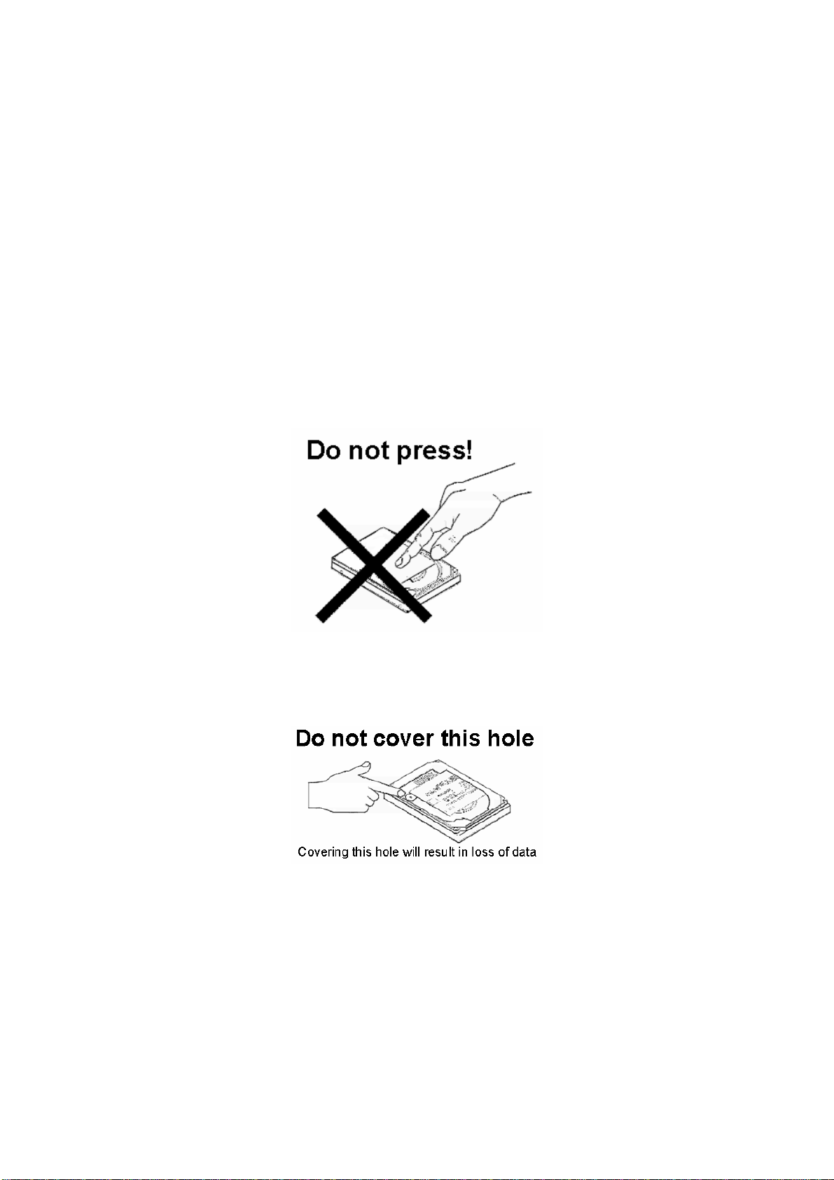
Do not apply force to the top cover (See figure below).
Do not cover the breathing hole on the top cover (See figure below).
Do not touch the interface connector pins or the surface of the printed circuit board.
The drive can be damaged by shock or ESD (Electric Static Discharge). Any damages incurred to
the drive after removing it from the shipping package and the ESD protective bag are the
responsibility of the user
1.4 Drive handling precautions
Do not press on the drive cover during handling.
12

5K320 SATA OEM Specification
2 Outline of the drive
2.5-inch, 9.5-mm Height
Perpendicular Recording
Formatted capacities of 320GB, 250GB, 160GB,120GB and 80GB(512 bytes/sector)
SATA Interface conforming to Serial ATA International Organization: Serial ATA Revision
2.6(15-February-2007)
Integrated controller
No-ID recording format
Coding : 100/102 2bit parity (199/200 RC Modulation Encoding)
Multi zone recording
Enhanced
Segmented Buffer with write cache
Fast data transfer rate
HTS5432xxL9A3xx model : up to 3.0Gbit/s
HTS5432xxL9SAxx model : up to 1.5Gbit/s
Media data transfer rate (max):
Average seek time: 12 ms for read
Closed-loop actuator servo (Embedded Sector Servo)
Rotary voice coil motor actuator
Load/Unload mechanism
Mechanical latch
ECC
10 bit 40 symbol non Interleaved Read Solomon code
Non interleave On-The –Fly correction
Included 2 symbol system ECC
8192 KB - Upper 1078KB is used for firmware
775 Mb/s
0.55 Watts at idle state
Power on to ready
3.5 sec
Operating shock
3920 m/sec2 (400 G)/2ms
1960 m/sec2 (200G)/1ms
Non operating shock
9800 m/sec2 (1000 G)/1ms
Bulk Encryption optional (HTS5432xxL9SAxx model only)
13

5K320 SATA OEM Specification
Part 1 Functional Specification
14

5K320 SATA OEM Specification
3 Fixed disk subsystem description
3.1 Control Electronics
The control electronics works with the following functions:
SATA Interface Protocol
Embedded Sector Servo
No-ID (TM) formatting
Multizone recording
Code: 100/102 bit parity (199/200 RC Modulation Encoding)
System ECC
Enhanced Adaptive Battery Life Extender
3.2 Head disk assembly data
The following technologies are used in the drive:
Femto Slider
Perpendicular recording disk a nd write head
TMR head
Integrated lead suspension (ILS)
Load/unload mechanism
Mechanical latch
15
5K320 SATA OEM Specification
4 Fixed disk characteristics
4.1 Formatted capacity by model number
Description
Physical Layout
Bytes per Sector 512 512
Number of Heads 4 4 / 3
Number of Disks 2 2
Logical Layout
Number of Heads 16 16
Number of Sectors/
Track
Number of
Cylinders
Number of Sectors 625,142,448 488,397,168
Total Logical Data
Bytes
Description
Physical Layout
Bytes per Sector 512 512 512
Number of Heads 2 2 1
Number of Disks 1 1 1
Logical Layout
Number of Heads 16 16 16
Number of Sectors/
Track
Number of
Cylinders
Number of Sectors 312,581,808 234,441,648 156,301,488
Total Logical Data
Bytes
HTS543232L9A300
HTS543232L9SA00
63 63
16,383 16,383
320,072,933,376 250,059,350,016
HTS543216L9A300
HTS543216L9SA00
63 63 63
16,383 16,383 16,383
160,041,885,696 120,034,123,776 80,026,361,856
HTS543225L9A300
HTS543225L9SA00
HTS543212L9A300
HTS543212L9SA00
HTS543280L9A300
HTS543280L9SA00
Table 1. Formatted capacity by model number.
16
5K320 SATA OEM Specification
4.2 Data sheet
Rotational Speed (RPM) 5400 5400 5400 5400 5400
Data transfer rates (buffer to/from
media) (Mbps)
Data transfer rates (Gbit/sec) 1.5/
Recording density (Kbit/mm) (Max)
(KBPI) (Max)
Track density (Ktrack/mm)(Max)
(KTPI)(Max)
Areal density (Kbit/sq-mm.- Max)
(Gbit/sq-inch - Max)
Number of zones 24 24 24 24 24
320
GB
729 775 729 674 729
3.0
1154 1207 1154 1066 1154
216 216
250 261
250
GB
1.5/
3.0
160
GB
1.5/
3.0
216
250
120
GB
1.5/
3.0
182
194
80
GB
1.5/
3.0
216
250
Table 2. Data sheet
4.3 Cylinder allocation
Data format is allocated by each head characteristics. Typical format is described below.
Zone
0 0 - 8187 1512
1 8188 - 12103 1476
2 12104 - 19045 1440
3 19046 - 26076 1404
4 26077 - 29903 1377
5 29904 - 35866 1350
6 35867 - 40672 1323
7 40673 - 49750 1269
8 49751 - 55624 1242
9 55625 - 59273 1224
10 59274 - 66126 1188
11 66127 - 72979 1134
12 72980 - 76717 1116
13 76718 - 85439 1080
14 85440 - 88910 1044
15 88911 - 92381 1026
16 92382 - 96831 999
17 96832 - 103239 972
18 103240 - 111160 918
19 111161 - 115432 891
20 115433 - 122374 864
21 122375 - 127625 810
22 127626 - 136258 756
23 136259 - 138305 729
Table 3. Cylinder allocation
160GB/p Mid BIP-Mid TPI format
Cylinder
No. of
Sectors/Trk
17

5K320 SATA OEM Specification
4.4 Performance characteristics
Drive performance is characterized by the following parameters:
Command Overhead
Mechanical Positioning
Seek Time
Latency
Data Transfer Speed
Buffering Operation (Look ahead/Write Cache)
Note: All the above parameters contribute to drive performance. There are other parameters which
contribute to the performance of the actual system. This specification defines the essential characteristics
of the drive. This specification does not include the system throughput as this is dependent upon the
system and the application.
The following table gives a typical value for each parameter.
Function
Average Random Seek Time - Read (ms) 12
Average Random Seek Time - Write (ms) 13
Rotational Speed (RPM) 5400
Power-on-to-ready (sec) 3.5
Command overhead (ms) 1.0
Disk-buffer data transfer (Mb/s) (max) 775
Buffer-host data transfer (Gbit/s) (max) 1.5 / 3.0
Table 4. Performance characteristics
4.4.1 Command overhead
Command overhead time is defined as the interval from the time that a drive receives a command to the
time that the actuator starts its motion.
18

5K320 SATA OEM Specification
4.4.2 Mechanical positioning
4.4.2.1 Average seek time (including settling)
Command Type Typical (ms) Max. (ms)
Read 12 14
Write 13 15
Table 5. Mechanical positioning performance
Typical and Max. are defined throughout the performance specification as follows:
Typical
Max.
The seek time is measured from the start of motion of the actuator to the start of a reliable read or write
operation. A reliable read or write operation implies that error correction/recovery is not employed to
correct arrival problems. The Average Seek Time is measured as the weighted average of all possible
seek combinations.
(max. + 1 – n)(Tn
Weighted Average = ––––––––––––––––––––––––––––
(max. + 1)(max)
Where: max. = maximum seek length
n = seek length (1-to-max.)
Tn
Tn
Average of the drive population tested at nominal environmental and voltage conditions.
Maximum value measured on any one drive over the full range of the environmental and
voltage conditions. (See section 6.1, "Environment" and section 6.2, "DC power
requirements" )
max.
in
out
+ Tn
n=1
= inward measured seek time for an n-track seek
= outward measured seek time for an n-track seek
in
out
)
4.4.2.2 Full stroke seek
Command Type Typical (ms) Max. (ms)
Read 20.0 25.0
Write 21.0 26.0
Table 6. Full stroke seek time
Full stroke seek time in milliseconds is the average time of 1000 full stroke seeks.
4.4.2.3 Single track seek time (without command overhead, including
settling)
Command Type Typical (ms) Maximum (ms)
Read 1.0 2.0
Write 1.1 2.2
Table 7. Single track seek time
Single track seek is measured as the average of one (1) single track seek from every track in both
directions (inward and outward).
4.4.2.4 Average latency
Rotational Speed
(RPM)
5400 11.1 5.5
Table 8. Latency time
Time for one revolution
(ms)
Average Latency
(ms)
19

5K320 SATA OEM Specification
4.4.2.5 Drive ready time
Condition Typical (sec) Max. (sec)
Power On To Ready 3.5 9.5
Table 9. Drive ready time
Ready
Power On To Ready
The condition in which the drive is able to perform a media access command
(for example—read, write) immediately.
This includes the time required for the internal self diagnostics.
20

5K320 SATA OEM Specification
4.4.3 Operating modes
Operating mode Description
Spin-Up
Seek
Write
Read
Performance idle
Active idle
Low power idle
Standby
Sleep
Table 10. Operating mode
Start up time period from spindle stop or power down.
Seek operation mode
Write operation mode
Read operation mode
The device is capable of responding immediately to media access requests. All
electronic components remain powered and the full frequency servo remain s
operational.
The device is capable of responding immediately to media access requests. Some
circuitry—including servo system and R/W electronics—is in power saving mode.
The head is parked near the mid-diameter the disk without servoing.
A device in Active idle mode may take longer to complete the execution of a
command because it must activate that circuitry.
The head is unloaded onto the ramp position. The spindle motor is rotating at full
speed.
The device interface is capable of accepting commands. The spindle motor is
stopped. All circuitry but the host interface is in power saving mode.
The execution of commands is delayed until the spindle becomes ready.
The device requires a soft reset or a hard reset to be activated. All electronics,
including spindle motor and host interface, are shut off.
4.4.3.1 Mode transition time
From To Transition
Time (typ)
Standby Idle 2.5 9.5
Table 11. Drive ready time
Transition Time
(max.)
4.4.3.2 Operating mode at power on
The device goes into Idle mode after power on or hard reset as an initial state..
4.4.3.3 Adaptive power save control
The transient timing from Performance Idle mode to Active Idle mode and Active Idle mode to Low Power
Idle mode is controlled adaptively according to the access pattern of the host system. The transient
timing from Low Power Idle mode to Standby mode is also controlled adaptively, if it is allowed by Set
Features Enable Advanced Power Management subcommand.
21

5K320 SATA OEM Specification
5 Data integrity
5.1 Data loss on power off
Data loss will not be caused by a power off during any operation except the write operation.
A power off during a write operation causes the loss of any received or resident data that has not
been written onto the disk media.
A power off during a write operation might make a maximum of one sector of data unreadable. This
state can be recovered by a rewrite operation.
5.2 Write Cache
When the write cache is enabled, the write command may complete before the actual disk write operation
finishes. This means that a power off, even after the write command completion, could cause the loss of
data that the drive has received but not yet written onto the disk.
In order to prevent this data loss, confirm the completion of the actual write operation prior to the power
off by issuing a
Soft reset
Hard reset
Flush Cache command
Standby command
Standby Immediate command
Sleep command
Confirm the command’s completion.
5.3 Equipment status
The equipment status is available to the host system any time the drive is not ready to read, write, or seek.
This status normally exists at the power-on time and will be maintained until the following conditions are
satisfied:
The access recalibration/tuning is complete.
The spindle speed meets the requirements for reliable operation.
The self-check of the drive is complete.
The appropriate error status is made available to the host system if any of the following conditions occur
after the drive has become ready:
The spindle speed lies outside the requirements for reliable operat ion.
The occurrence of a Write Fault condition.
5.4 WRITE safety
The drive ensures that the data is written into the disk media properly. The following conditions are
monitored during a write operation. When one of these conditions exceeds the criteria, the write operation
is terminated and the automatic retry sequence is invoked.
Head off track
External shock
Low supply voltage
Spindle speed out of tolerance
Head open/short
22

5K320 SATA OEM Specification
5.5 Data buffer test
The data buffer is tested at power on reset and when a drive self-test is requested by the host. The test
consists of a write/read '00'x and 'ff'x pattern on all buffers.
5.6 Error recovery
Errors occurring on the drive are handled by the error recovery procedure.
Errors that are uncorrectable after application of the error recovery procedure are reported to the host
system as nonrecoverable errors.
5.7 Automatic reallocation
The sectors that show some errors may be reallocated automatically when specific conditions are met.
The drive does not report any auto reallocation to the host system. The conditions for auto reallocation
are described below.
5.7.1 Nonrecovered write errors
When a write operation cannot be completed after the Error Recovery Procedure (ERP) is fully carried out,
the sectors are reallocated to the spare location. An error is reported to the host system only when the
write cache is disabled and the auto reallocation has failed.
5.7.2 Nonrecoverable read error
When a read operation fails after ERP is fully carried out, a hard error is reported to the host system. This
location is registered internally as a candidate for the reallocation. When a registered location is specified
as a target of a write operation, a sequence of media verification is performed automatically. When the
result of this verification meets the required criteria, this sector is reallocated.
5.7.3 Recovered read errors
When a read operation for a sector fails and is recovered at the spe cific ERP ste p, the sector is
reallocated automatically. A media verification sequence may be run prior to the reallocation according to
the predefined conditions.
23

5K320 SATA OEM Specification
5.8 ECC
The 10 bit symbol non interleaved ECC processor provides user data verification and correction
capability. The first 6 symbol of ECC are 4 check symbols for user data and the 2 symbol system ECC.
The other 34 symbols are Read Solomon ECC. Hardware logic corrects up to 16 symbols(20 bytes)
errors on-the-fly.
2 symbol System ECC is generated when HDC receives user data from HOST, and can correct up to 1
symbol(10bit) errors on-the-fly when one transfers to HOST.
24

5K320 SATA OEM Specification
6 Specification
6.1 Environment
6.1.1 Temperature and humidity
Operating conditions
Temperature
Relative humidity
Maximum wet bulb temperature
Maximum temperature gradient
Altitude
Nonoperating conditions
Temperature
Relative humidity
Maximum wet bulb temperature
Maximum temperature gradient
Altitude
Table 12. Environmental condition
The system is responsible for providing sufficient air movement to maintain surface tem peratures below
60°C at the center of top cover and below 63°C at the center of the drive circuit board assembly.
5 to 55°C (See note below)
8 to 90% noncondensing
29.4°C noncondensing
20°C/hour
–300 to 3048 m (10,000 ft)
–40 to 65°C
5 to 95% noncondensing
40°C noncondensing
20°C/hour
–300 to 12,192 m (40,000 ft)
The maximum storage period in the shipping package is one year.
Sp e c if ic a t ion ( E n v ir o n m e n t )
100
90
80
70
60
31'C/90%
41'C/95%
W etBulb 40'C
W e tBulb29.4'C
Non Operating
50
40
Relative Humidity (%)
30
20
10
0
-45-35-25-15 -5 5 15 25 35 45 55 65
Temperatur e (degC)
Operating
55'C/15%
Figure 1. Limits of temperature and humidity
65'C/23%
6.1.2 Corrosion test
The hard disk drive must be functional and show no signs of corrosion after being expose d to a
temperature humidity stress of 50°C/90%RH (relative humidity) for one week followed by a temperature
and humidity drop to 25'C/40%RH in 2 hours.
25

5K320 SATA OEM Specification
6.1.3 Radiation noise
The disk drive shall work without degradation of the soft error rate under the following magnetic flux
density limits at the enclosure surface.
Frequency (KHz) Limits (uT RMS)
DC 1500 0-p
0 < Frequency =< 60 500 RMS
60 < Frequency =<100 250 RMS
100 < Frequency =< 200 100 RMS
200 < Frequency =< 400 50 RMS
Table 13. Magnetic flux density limits
6.1.4 Conductive noise
The disk drive shall work without soft error degradation in the frequency range from DC to 20 Mhz
injected through any two of the mounting screw holes of the drive when an AC current of up to 45 mA
(p-p) is applied through a 50-ohm resistor connected to any two mounting screw holes.
26

5K320 SATA OEM Specification
6.2 DC power requirements
Connection to the product should be made in a safety extra low voltage (SELV) circuits. The voltage
specifications are applied at the power connector of the drive.
Item Requirements
Nominal supply +5 Volt dc
Supply voltage –0.3 Volt to 6.0 Volt
Power supply ripple (0–20
1
MHz)
Tolerance 2
Supply rise time 1–100 ms
Performance Idle average 3
Active Idle average 0.8
Low Power Idle average 0.55
Read average 4
Write average 1.8
Seek average 5
Standby 0.2
Sleep 0.1
Startup (maximum peak) 6
Average from power on to
ready
Table 14. DC Power requirements
Watts (RMS Typical)
7
100 mV p-p max.
±5%
1.7
1.8
2.2
5.0
3.8
Footnotes:
1. The maximum fixed disk ripple is measured at the 5 volt input of the drive.
2. The disk drive shall not incur damage for an over voltage condition of +25% (m aximum
3. The idle current is specified at an inner track.
4. The read/write current is specified based on three operations of 63 sector read/write per
5. The seek average current is specified based on three operations pe r 100 ms.
6. The worst case operating current includes motor surge.
7. “Typical” mean average of the drive population tested at nominal environmental and
duration of 20 ms) on the 5 volt nominal supply.
100 ms.
voltage conditions.
27

5K320 SATA OEM Specification
6.2.1 Power consumption efficiency
Capacity 320GB 250GB 160GB 120GB 80GB
Power Consumption Efficiency
(Watts/GB)
0.0017 0.0022 0.0034 0.0046 0.0069
Table 15. Power consumption efficiency
Note: Power consumption efficiency is calculated as Power Consumption of Low Power Idle Watt/
Capacity (GB).
28

5K320 SATA OEM Specification
6.3 Reliability
6.3.1 Data reliability
Probability of not recovering data is 1 in 10
ECC implementation
On-the-fly correction performed as a part of read channel function recovers up to 16 symbols of error in 1
sector (1 symbol is 10 bits).
14
bits read
6.3.2 Failure prediction (S.M.A.R.T.)
The drive supports Self-monitoring, analysis and reporting technology (S.M.A.R.T.) function. The details
are described in section 11.8, "S.M.A.R.T. Function" and in Section 13.32, "S.M.A.R.T. Function Set
(B0h)"
6.3.3 Cable noise interference
To avoid any degradation of performance throughput or error when the interface cable is route d on top or
comes in contact with the HDA assembly, the drive must be grounded electrically to the system frame by
four screws. The common mode noise or voltage level difference between the system frame and power
cable ground or AT interface cable ground should be in the allowable level specified in the power
requirement section.
6.3.4 Service life and usage condition
The drive is designed to be used under the following conditions:
The drive should be operated within specifications of shock, vibration, temperature, humidity, altitude,
and magnetic field.
The drive should be protected from ESD.
The breathing hole in the top cover of the drive should not be covered.
Force should not be applied to the cover of the drive.
The specified power requirements of the drive should be satisfied.
The drive frame should be grounded electrically to the system through four screws.
The drive should be mounted with the recommended screw depth and torque.
The interface physical and electrical requirements of the drive should satisfy Serial ATA Revision 2.6.
The power-off sequence of the drive should comply with the 6.3.6.2,"Required power-off
sequence.”
Service life of the drive is approximately 5 years or 20,000 power on hours, whichever comes first, under
the following assumptions:
Less than 333 power on hours per month.
Seeking/Writing/Reading operation is less than 20% of power on hours.
This does not represent any warranty or warranty period. Applicable warranty and warranty period are
covered by the purchase agreement.
29

5K320 SATA OEM Specification
6.3.5 Preventive maintenance
None.
6.3.6 Load/unload
The product supports a minimum of 600,000 normal load/unloads.
Load/unload is a functional mechanism of the hard disk drive. It is controlled by the drive micro code.
Specifically, unloading of the heads is invoked by the following commands:
Standby
Standby immediate
Sleep
Load/unload is also invoked as one of the idle modes of the drive.
The specified start/stop life of the product assumes that load/unload is operated normally, not in
emergency mode.
6.3.6.1 Emergency unload
When hard disk drive power is interrupted while the heads are still loaded the micro code cannot operate
and the normal 5-volt power is unavailable to unload the heads. In this case, normal unload is not
possible. The heads are unloaded by routing the back EMF of the spinning motor to the voice coil. The
actuator velocity is greater than the normal case and the unload process is inherently less controllable
without a normal seek current profile.
Emergency unload is intended to be invoked in rare situations. Because this operation is inherently
uncontrolled, it is more mechanically stressful than a normal unload.
The drive supports a minimum of 20,000 emergency unloads.
6.3.6.2 Required Power-Off Sequence
The required host system sequence for removing power from the drive is as follows:
Step 1: Issue one of the following commands.
Standby
Standby immediate
Sleep
Note: Do not use the Flush Cache command for the power off sequence because this command
does not invoke Unload.
Step 2: Wait until the Command Complete status is returned.
In a typical case 500 ms are required for the command to finish completion; however, the host system
time out value needs to be 30 seconds considering error recovery time.
Step 3: Terminate power to HDD.
This power-down sequence should be followed for entry into any system power-down state, system
suspend state, or system hibernation state. In a robustly designed system, emergency unload is limited
to rare scenarios, such as battery removal during operation.
6.3.6.3 Power switch design considerations
In systems that use the Travelstar 5K320 consideration should be given to the design of the system
power switch.
Hitachi recommends that the switch operate under control of the host system, as opposed to being
hardwired. The same recommendation is made for cover-close switches. When a hardwired switch is
30
 Loading...