

Hitachi HTDK-185-UK Service manual

SERVICE MANUAL
MANUEL D'ENTRETIEN
WARTUNGSHANDBUCH
CAUTION:
Before servicing this chassis, it is important that the service technician read the “Safety
Precautions” and “Product Safety Notices” in this service manual.
SM0154
HTD-K185UK
Data contained within this Service
manual is subject to alteration for
improvement.
ATTENTION:
Avant d’effectuer l’entretien du châassis, le technicien doit lire les «Précautions de sécurité»
et les «Notices de sécurité du produit» présentés dans le présent manuel.
VORSICHT:
Vor Öffnen des Gehäuses hat der Service-Ingenieur die „Sicherheitshinweise“ und „Hinweise
zur Produktsicherheit“ in diesem Wartungshandbuch zu lesen.
Les données fournies dans le présent
manuel d’entretien peuvent faire l’objet
de modifications en vue de perfectionner
le produit.
Die in diesem Wartungshandbuch
enthaltenen Spezifikationen können sich
zwecks Verbesserungen ändern.
SPECIFICATIONS AND PARTS ARE SUBJECT TO CHANGE FOR IMPROVEMENT
DVD AV Receiver and Digital Terrestrial TV Receiver
October 2004

A) HARDWARE
1. GENERAL DESCRIPTION
1.1 MT1379
The MT1379 Progressive Scan DVD-Player Combo Chip is a single-chip MPEG video
decoding chip that integrates audio/video stream data processing, TV encoder, four video
DACs with Macrovision, copy protection, DVD system navigation, system control and
housekeeping functions.
The features of this chip can be listed as follows;
General Features:
* Progressive scan DVD-player combo chip
* Integrated NTSC/PAL encoder,
* Built-in progressive video output
* DVD-Video, VCD 1.1, 2.0, and SVCD,
* Unified track buffer and A/V decoding buffer,
* Direct interface of 32-bit SDRAM,
* Servo controller and data channel processing.
Video Related Features:
* Macrovision 7.1 for NTSC/PAL interlaced video,
* Simultaneous composite video and S-video outputs, or composite and YUV outputs,
or composite and RGB outputs.
* 8-bit CCIR 601 YUV 4:2:2 output.
* Decodes MPEG video and MPEG2 main profile at main level.
* Maximum input bit rate of 15Mbits/sec.
Audio Related Features:
* Dolby Digital (AC-3) and Dolby Pro Logic
* Dolby Digital S/PDIF digital audio output
* High-Definition Compatible Digital. (HDCD) decoding
* Dolby Digital Class A and HDCD certified
* SRS True Surround
* CD-DA
* MP3

1.2 Memory
SDRAM Memory Interface
The MT1379 provides a glueless 16-bit interface to DRAM memory devices used as
OSD, MPEG stream and video buffer memory for a DVD player. The maximum amount of
memory support is 16 MB of Synchronous DRAM (SDRAM). The memory interface is
configurable in depth to support 128-Mb addressing. The memory interface controls
access to both external SDRAM memories, which can be the sole unified external
read/write memory acting as program and data memory as well as various decoding and
display buffers.
1.3 Drive Interfaces
The MT1379 supports the DV34 interface, and other RF and servo interfaces used
by many types of DVD loaders. These interfaces meet the specifications of many DVD
loader manufacturers.
1 . 4 Front Panel
The front panel is based around a Futaba VFD and a common NEC front panel
controller chip, (uPD16311). The MT1379 controls the uPD16311 using several control
signals, (clock, data, chip select). The infrared remote control signal is passed directly to
the MT1379 for decoding.
1.5 Rear Panel
A typical rear panel is included in the reference design. This rear panel supports:
• Six channel or two channel audio outputs,
• Optical and coax SPDIF outputs,
• Composite, S-Video, and SCART outputs.
The six-video signals used to provide CVBS, S-Video, and RGB are generated by the
MT1379's internal video DAC, The video signals are buffered by external circuitry.
Six channel audio output by the MT1379 in the form of three I2S (or similar) data
streams. The S/ PDIF serial stream is also generated by the MT1379 output by the rear
panel. The six channel audio DACs (AK4356, PCM1606) are used for six channel audio
output with MT1379, and similarly AK4382A, CS4392 Audio DACs are used for two
channel audio output with MT1379.
12-pin DDX board output jack gives out the amplified audio. Digital Audio is processed
in the DDX-8228 IC and then amplified in the DDX-2050 Power Amplifier ICs.
2. SYSTEM BLOCK DIAGRAM AND MT1379 PIN DECRIPTION
2.1 MT1379 Pin Description
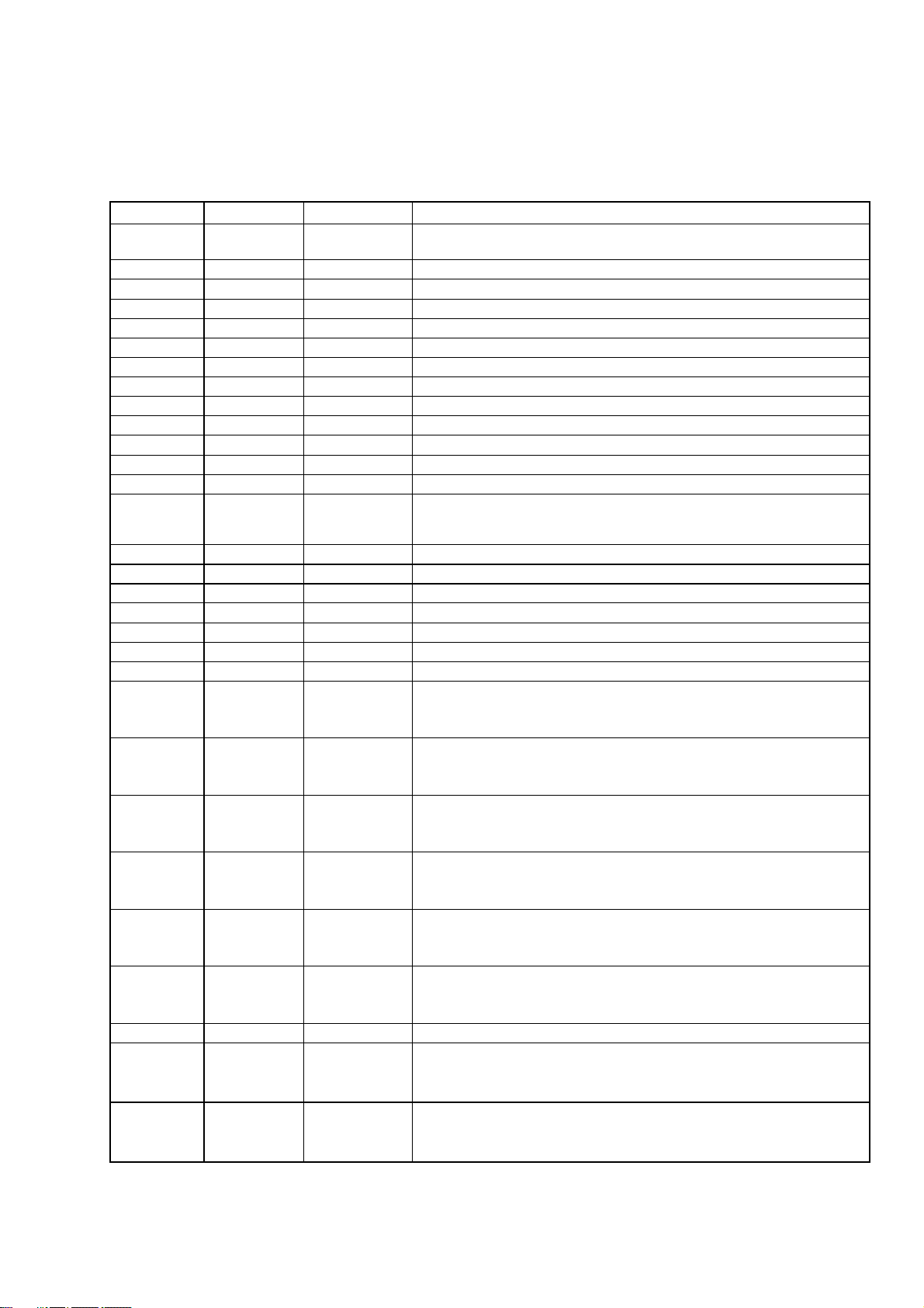
Pin Number Symbol Type Description
1 IREF Analog Input
2 PLLVSS Ground Ground pin for data PLL and related analog circuitry
3 LPIOP Analog Output Positive output of the low pass filter
4 LPION Analog Output Negative output of the low pass filter
5 LPFON Analog output Negative output of loop filter amplifier
6 LPFIP Analog Input Positive input of loop filter amplifier
7 LPFIN Analog Input Negative input of loop filter amplifier
8 LPFOP Analog Output Positive output of loop filter amplifier
9 JITFO Analog Output RF jitter meter output
10 JITFN Analog Input Negative input of the operation amplifier for RF jigger meter
11 PLLVDD3 Power 3.3V power pin for data PLL and related analog circuitry
12 FOO Analog Output Focus servo output. PDM output of focus servo compensator
13 TRO Analog Output Tracking servo output. PDM output of tracking servo compensator
14 TROPENPWM Analog Output
15 PWMOUT1 Analog Output The 1st general PWM output
16 PWMOUT2 Analog Output The 2nd general PWM output
17 DVDD2 Power 2.5V power pin for internal fully digital circuitry
18 DMO Analog Output Disk motor control output. PWM output
19 FMO Analog Output Feed motor control. PWM output
20 DVSS Ground Ground pin for internal fully digital circuitry
21 FG Input ^1 Motor Hall sensor input
22 HIGHAO
Inout 2-16 MA,
SR PU
Current reference input. It generates reference current for data PLL. Connect
an external 100K resistor to this pin and PLLVSS.
Tray open output, controlled by microcontroller. This is PWM output
for TRWMEN27hRW2=1 or is digital output for TRWMEN27hRW2=0
Microcontroller address 8
23 HIGHA1
24 HIGHA2
25 HIGHA3
26 HIGHA4
27 HIGHA5
28 DVSS Ground Ground pin for internal digital circuitry
29 HIGHA6
30 HIGHA7
Inout 2-16
MA, SR PU
Inout 2-1 6MA,
SR PU
Inout 2-16MA,
SR PU
Inout 2-16MA,
SR PU
Inout 2-16MA,
SR PU
Inout 2-16MA,
SR PU
Inout 2-16MA,
SR PU
Microcontroller address 9
Microcontroller address 10
Microcontroller address 11
Microcontroller address 12
Microcontroller address 13
Microcontroller address 14
Microcontroller address 15
31 AD7
Inout 2-16MA,
SR
Microcontroller address/data 7
32 AD6
33 ADS
34 AD4
35 DVDD3 Power 3.3V power pin for internal digital circuitry
36 ADS
37 AD2
38 AD1
39 ADO
40 IOAO
41 IOA1
42 DVDD2 Power 2.5V power pin for internal digital circuitry
43 IOA2
Inout 2-16MA,
SR
Inout 2-16MA,
SR
Inout 2-16MA,
SR
Inout 2-16MA,
SR
Inout 2-16MA,
SR
Inout 2-16MA,
SR
Inout 2-16MA,
SR
Inout 2-16MA,
SR PU
Inout 2-16MA,
SR PU
Inout 2-16MA,
SR PU
Microcontroller address/data 6
Microcontroller address/data 5
Microcontroller address/data 4
Microcontroller address/data 3
Microcontroller address/data 2
Microcontroller address/data 1
Microcontroller address/data 0
Microcontroller address 0 / IO
Microcontroller address 1 / IO
Microcontroller address 2 / IO
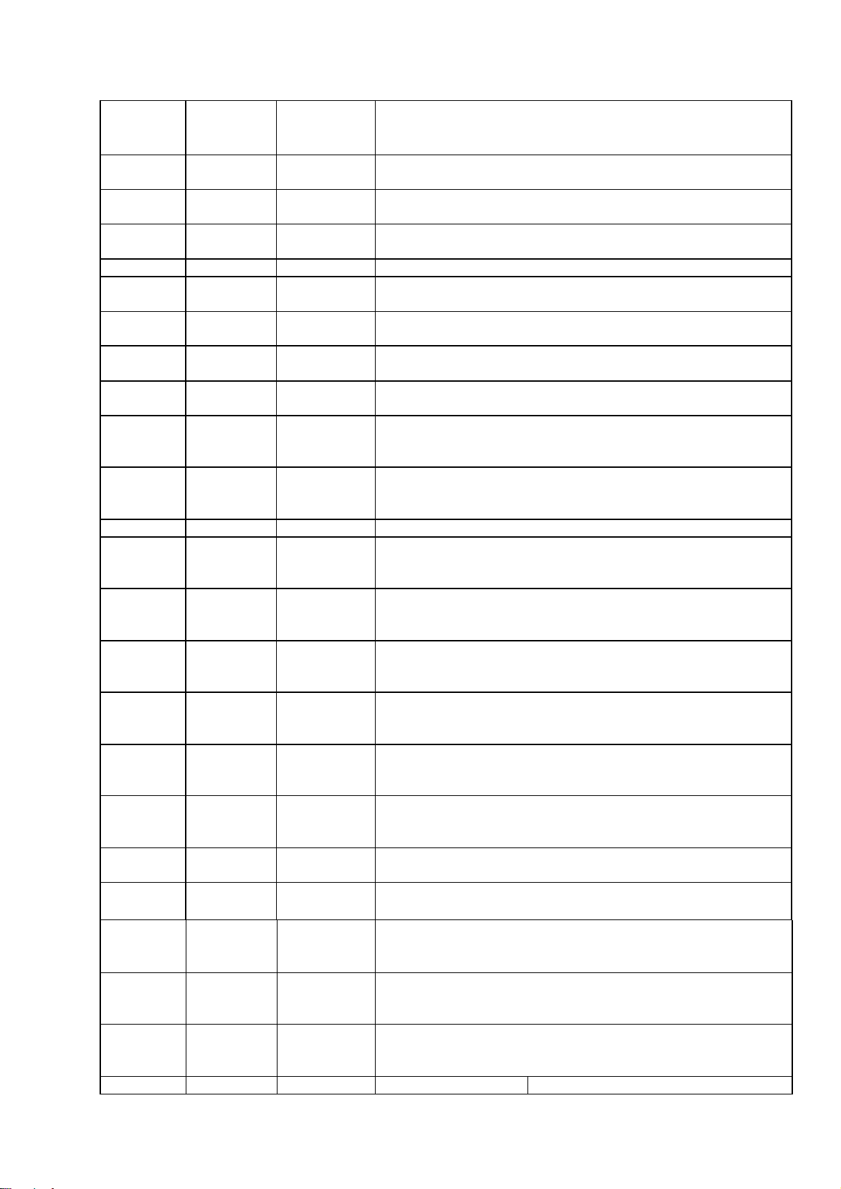
44
45 IOA4
46 IOA5
47 IOA6
48 IOA7
49 A16
50 A17
51 IOA18
52 IOA19
Inout 2-16 MA,
SR PU
Inout 2-16MA,
SR PU
Inout 2-16MA,
SR PU
Inout 2-16MA,
SR PU
Inout 2-16MA,
SR PU
Output
2-16MA, SR
Output
2-16MA, SR
Inout 2-16MA,
SR SMT
Inout 2-16MA,
SR SMT
Microcontroller address 3 / IO
Microcontroller address 4 / IO
Microcontroller address 5 / IO
Microcontroller address 6 / IO
Microcontroller address 7 / IO
Flash address 16
Flash address 17
Flash address 18 /IO
Flash address 19 /IO
53 IOA20
54 APLLVSS Ground
Inout 2-16MA,
SR SMT
Flash address 20 / IO OR
Video in Data PortB 0
Ground pin for audio clock
circuitry
55 APLLVDD3 Power
56 ALE
57 IOOE#
Inout 2-16MA,
SR PU, SMT
Inout 2-16MA,
SR SMT
3.3V Power pin for audio clock circuitry
Microcontroller address latch enable
Flash output enable, active low / IO
58 IOWR#
59 IOCS#
60 DVSS Ground
61 UP1_2
62 UP1_3
63 UP1_4
64 UP1_5
65 UP1_6
66 DVDD3 Power 3.3V power pin for internal digital circuitry
67 UP1_7
68 UP3_0
69 UP3_1
70 INTO#
Inout 2-16MA,
SR SMT
Inout 2-16MA,
SR PU, SMT
Inout 4MA,
SR PU,
SMT
Inout 4MA,
SR PU, SMT
Inout 4MA,
SR PU,
SMT
Inout 4MA,
SR PU,
SMT
Inout 4MA,
SR PU,
SMT
Inout 4MA,
SR PU,
SMT
Inout 4MA,
SR PU,
SMT
Inout 4MA,
SR PU,
SMT
Inout 2-16MA,
SR PU, SMT
Flash write enable, active low / IO
Flash chip select, active low / IO
Ground pin for internal digital circuitry
Microcontroller port 1-2
Microcontroller port 1-3
Microcontroller port 1-4
Microcontroller port 1-5
Microcontroller port 1-6
Microcontroller port 1-7
Microcontroller port 3-0
Microcontroller port 3-1
Microcontroller interrupt 0, active low
71 IR
72 DVDD2 Power 2.5V power pin for internal digital circuitry
73 UPS 4 Inout Microcontroller port 3-4
74 UPS 5 Inout Microcontroller port 3-5
75 UWR#
76 URD#
77 DVSS Ground Ground pin for internal digital circuitry
78 RD7 Inout DRAM data 7
79 RD6 Inout DRAM data 6
80 RD5 Inout DRAM data 5
81 RD4 Inout DRAM data 4
82 DVDD2 Power 2.5V power pin for internal digital circuitry
Input SMT
Inout 2-16MA,
SR PU, SMT
Inout 2-16MA,
SR PU, SMT
IR control signal input
Microcontroller write strobe, active low
Microcontroller read strobe, active low
83 RD3 Inout DRAM data 3
84 RD2 Inout DRAM data 2
85 RD1 Inout DRAM data 1
86 RDO Inout DRAM data 0
87
88 CAS#
89 RAS#
90 RCS#
91 BAO
92 DVSS Ground Ground pin for internal digital circuitry
93 RD15
94 RD14
95 RD13
96 RD12
97 DVDD3 Power 3.3V power pin for internal digital circuitry
98 RD11
99 RD10
100 RD9
101 RD8
102 DVSS Ground Ground pin for internal digital circuitry
103 CLK
104 CLE
105 RA11
106 RA9
107 RA8
108 DMVDD3 Power 3.3V Power pin for DRAM clock circuitry
109 DMVSS Ground Ground pin for DRAM clock circuitry
110 RA7
111 DVDD3 Power I % 3.3V power pin for internal digital circuitry
RWE#
Output
2-16MA, SR
Output
2-16MA, SR
Output
2-16MA, SR
Output
2-16MA, SR
Output
2-1 6MA, SR
Inout 2-16MA,
SR PU/PD,
SMT
Inout 2-16MA,
SR PU/PD,
SMT
Inout 2-16MA,
SR PU/PD,
SMT
Inout 2-16MA,
SR PU/PD,
SMT
Inout 2-16MA,
SR PU/PD,
SMT
Inout 2-16MA,
SR PU/PD,
SMT
Inout 2-16MA,
SR PU/PD,
SMT
Inout 2-16MA,
SR PU/PD,
SMT
Output
2-1 6MA, SR
Output
2-16MA, SR
Output
2-16MA, SR
Output
2-16MA, SR
Output
2-16MA, SR
Output
2-16MA, SR
DRAM Write enable, active low
DRAM column address strobe, active low
DRAM row address strobe, active low
DRAM chip select, active low
DRAM bank address 0
DRAM data 15
DRAM data 14
DRAM data 13
DRAM data 12
DRAM data 11
DRAM data 10
DRAM data 9
DRAM data 8
DRAM clock
DRAM clock enable
DRAM address bit 1 1 or audio serial data 3 (channel 7/8)
DRAM address 9
DRAM address 8
DRAM address 7
112 RA6
113 RA5
114 RA4
115 DVSS Ground Ground pin for internal digital circuitry
116 DQM1
117 DQMO
118 BA1
119 RA10
120 DVDD2 Power 2.5V power pin for internal digital circuitry
121 RAO
122 RA1
123 RA2
124 RA3
125
126
127
128
129
130
131
132
133
134
DVSS
RD31
RD30
RD29
RD28
DVDD3
RD27
RD26
RD25
RD24
135
136
137
DVSS
DQM3
DQM2
Output
2-16MA, SR
Output
2-16MA, SR
Output
2-16MA, SR
Output
2-16MA, SR
Output
2-16MA, SR
Output
2-16MA, SR
Output
2-16MA, SR
Output
2-16MA, SR
Output
2-16MA, SR
Output
2-16MA, SR
Output
2-16MA, SR
Ground
Inout 2-16MA,
SR PU/PD,
SMT
Inout 2-16MA,
SR PU/PD,
SMT
Inout 2-16MA,
SR PU/PD,
SMT
Inout 2-16MA,
SR PU/PD,
SMT
Power
Inout 2-16MA,
SR PU/PD,
SMT
Inout 2-16MA,
SR PU/PD,
SMT
Inout 2-16MA,
SR PU/PD,
SMT
Inout 2-16MA,
SR PU/PD,
SMT
Ground
Output
2-1 6MA, SR
Output
2-1 6MA, SR
DRAM address 6
DRAM address 5
DRAM address 4
Mask for DRAM input/output byte 1
Mask for DRAM input/output byte 0
DRAM bank address 0
DRAM address lO
DRAM address 0
DRAM address 1
DRAM address 2
DRAM address 3
Ground pin for internal digital circuitry
DRAM data 31
DRAM data 30
DRAM data 29
DRAM data 28
3.3V power pin for internal digital circuitry
DRAM data 27
DRAM data 26
DRAM data 25
DRAM data 24
Ground pin for internal digital circuitry
Mask for DRAM input/output byte 3
Mask for DRAM input/output byte 2
138
139
140
141
142
143 RD19
144 RD18
145 DVSS Ground Ground pin for internal digital circuitry
146 RD17
147 RD16
148 ABCK
149 ALRCK
150 DVDD3 Power 3.3V power pin for internal digital circuitry
151 ACLK
152 MC DATA Input Microphone serial input
153 SPDIF
RD23
RD22
DVDD2
RD21
RD20
Inout 2-16MA,
SR PU/PD,
SMT
Inout 2-16MA,
SR PU/PD,
SMT
Power
Inout 2-16MA,
SR PU/PD,
SMT
Inout 2-16MA,
SR PU/PD,
SMT
Inout 2-16MA,
SR PU/PD,
SMT
Inout 2-16MA,
SR PU/PD,
SMT
Inout 2-16MA,
SR PU/PD,
SMT
Inout 2-16MA,
SR PU/PD,
SMT
Output
4MA
Inout 4MA,
PD, SMT
Inout
4MA
Output 2-16MA,
SR : ON/OFF
DRAM data 23 / Videoin
Data PortA 7
DRAM data 22 / Videoin
Data PortA 6
2.5V power pin for internal digital circuitry
DRAM data 21 / Videoin
Data PortA 5
DRAM data 20 / Videoin
Data PortA 4
DRAM data 19 /
Videoin Data PortA 3
DRAM data 18 /
Videoin Data PortA 2
DRAM data 17 /
Videoin Data PortA 1
DRAM data 16 /
Videoin Data PortA 0
Audio bit clock
(1 ) Audio left/right channel clock
(2) Trap value in power-on reset :
1 : use external 373 0: use internal 373
Audio DAC master clock (384/256 audio sample frequency)
SPDIF output
154 ASDATAO
155 ASDATA1
156
ASDATA2
157 ASDATA3
158 ASDATA4
159 DACVDDC Power 3.3V power pin for VIDEO DAC circuitry
160 VREF Analog input
161 FS Analog output
Inout 4MA
PDSMT
Inout 4MA
PD SMT
Inout 4MA
PD SMT
Inout 4MA
PD SMT
Inout 4MA
PD SMT
(1 ) Audio serial data 0 (left/right channel)
(2) Trap value in power-on reset :
1 : manufactory test mode 0 : normal operation
(1) Audio serial data 1 (surround left/surround right channel)
(2) Trap value in power-on reset :
1 : manufactory test mode 0 : normal operation
(1 ) Audio serial data 2 (center/left channel)
(2) Trap value in power-on reset :
1 : manufactory test mode 0 : normal operation
(1 ) Audio serial data 3 (surround left/surround right channel)
(2) Trap value in power-on reset :
1 : manufactory test mode 0 : normal operation OR Videoin Data PortB 1
(1 ) Audio serial data 4 (center/left channel)
(2) Trap value in power-on reset :
1 : manufactory test mode 0 : normal operation OR Videoin Data PortB 2
Bandgap reference voltage
Full scale adjustment
162 YUVO/CIN
163 DACVSSC Ground
164 YUV1/C
165 DACVDDB Power 3.3V power pin for VIDEO DAC circuitry
166 YUV2/Y
167 DACVSSB Ground Ground pin for VIDEO DAC circuitry
168 YUV3/CVBS
169 DACVDDA Power 3.3V power pin for VIDEO DAC circuitry
170 YUV4/G
171 DACVSSA Ground Ground pin for VIDEO DAC circuitry
172 YUV5/B
173 YUV6/R
174 ICE
175 BLANK#
176 VSYN
177 YUV7
178 DVSS Ground Ground pin for internal digital circuitry
179 HSYN
180 SPMCLK Input
181 SPDATA Input
182 DVDD2 Power 2.5V power pin for internal digital circuitry
183 SPLRCK Input
184 SPBCK Input
185 DVDD3 Power 3.3V power pin for internal digital circuitry
186 XTALO Output Crystal output
187 XTALI Input Crystal input
188 PRST
189 DVSS Ground Ground pin for internal digital circuitry
190 VFO13 Output The 1st, 3rd header VFO pulse output
191 IDGATE Output Header detect signal output
192 DVDD3 Power 3.3V power pin for internal digital circuitry
Output
4MA, SR
Output
4MA, SR
Output
4MA, SR
Output
4MA, SR
Output
4MA, SR
Output
4MA, SR
Output
4MA, SR
Input PD,
SMT
Inout 4MA,
SR SMT
Inout 4MA,
SR SMT
Inout 4MA,
SR SMT
Inout I4MA,
SR SMT
Input PD,
SMT
Video data output bit 0 /
Compensation capacitor
Ground pin for VIDEO DAC circuitry
Video data output bit 1 /
Analog chroma output
Video data output bit 2 /
Analog Y output
Video data output bit 3 /
Analog composite output
Video data output bit 4 /
Green or Y
Video data output bit 5 /
Blue or CB
Video data output bit 6 / Red
or CR
Microcontroller ICE mode enable
Video blank area, active low /
Videoin Field_601
Vertical sync / Videoin
Vsync_601
Video data output bit 7 / Videoin Data
PortB 3
Horizontal sync /
Videoin Hsync_601
Audio DAC master clock of SPDIF input /
Videoin Data PortB 4
Audio data of SPDIF input /
Videoin Data PortB 5
Audio left/right channel clock of SPDIF input /
Videoin Data PortB 6
Audio bit clock of SPDIF input /
Videoin Data PortB 7
Power on reset input, active high
193 UDGATE Output DVD_RAM recording data gate signal output
194 WOBSI Input Wobble signal input
195 SDATA Output RF serial data output
196 SDEN Output RF serial data latch enable
197 SLCK Output RF serial clock output
198 EDO Input Flag of defect data input status
199 ADCVSS Ground Ground pin for ADC circuitry
200 ADIN Analog Input General A/D input
201 RFSUBI Analog Input RF subtraction signal input terminal
202 TEZISLV Analog Input Tracking error zero crossing low pass input
203 TEI Analog Input Tracking error input
204 CSO Analog Input Central servo input
205 FEI Analog Input Focus error input
206 RFLEVEL Analog Input Sub beam add input or RFRP low pass input
207 RFRP DC A Input RF ripple detect input
208 RFRP AC Analog Input RF ripple detect input (through AC coupling)
209 HRFZC Analog Input High frequency RF ripple zero crossing
210 PWMVREF A Input A reference voltage input for PWM circuitry. A typical value of 4.0 v
211 PWM2VREF A Input A reference voltage input for PWM circuitry. A typical value of 2.0 v
212 ADCVDD3 Power 3.3V power pin for ADC circuitry
213 RFDTSLVP Analog Output Positive RF data slicer level output
214 RFDTSLVN Analog Output Negative RF data slicer level output
215 RFIN Analog Input Negative input of RF differential signal
216 RFIP Analog Input Positive input of RF differential signal
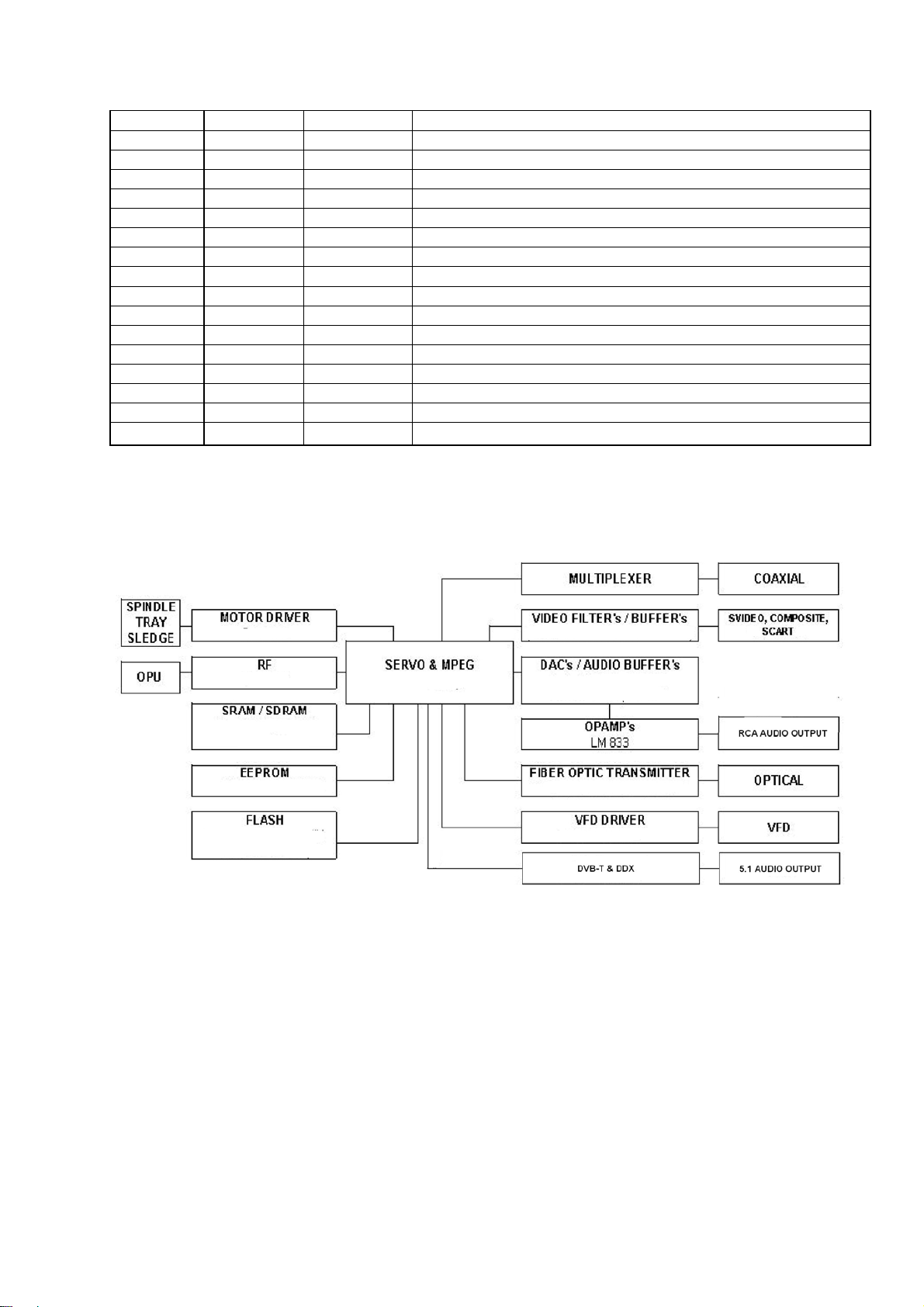
2.2 System Block Diagram
A sample system block diagram for AV1100 board design is shown in the following figure:
3. AUDIO OUTPUT
The MT1379 supports two-channel and six-channel analog audio output. In a system
configuration with six analog outputs, the front left and right channels can be configured
to provide the stereo (2 channel) outputs and Dolby Surround, or the left and rig ht fron t
channels for a 5.1 channel surround system.
The MT1379 also provides digital output in SPDIF format. The board supports both
optical and coaxial SPDIF outputs,
4. AUDIO DACS
The MT1379 supports several variations of an PS type bus, varying the order of the
data bits (leading or no leading zero bit, left or right alignment within frame, and M SB or

LSB first) is possible using the MT1379 internal configuration registers. The I2S format
uses four stereo data lines and three clock lines. The PS data and clock lines can be
connected directly to one or more audio DAC to generate analog audio output.
The two-channel DAC is a CS4392, The DACs support up to 192kHz sampling rate.
The outputs of the DACs are differential, not single ended so a buffering circuit is
required. The buffer circuits use National LM833 op-amps to perform the low-pass
filtering and the buffering,
5 VIDEO INTERFACE
5.1 Video Display Output
The video output section controls the transfer of video frames stored in memory to the
internal TV encoder of the MT1379, The outp u t s e c ti o n c o n si s t s o f a p ro g r a mm a b le C R T
controller capable of operating either in Master or Slave mode.
The video output section features internal line buffers which allow the outgoing
luminance and chrominance data to match the internal clock rates with external pixel
clock rates, easily facilitating YUV 4:2:2 to YUV 4:2:0 component and sample
conversion, A polyphase filter achieves arbitr ary horizontal decimation and interpolation.
Video Bus
The video bus has 8 YUV data pins that transfer luminance and chrominance (YUV)
pixels in CCIR601 pixel format (4:2:2), In this format, there are half as many
chrominance (U or V) pixels per line as luminance (Y) pixels; there are as many
chrominance lines as luminance,
Video Post-Processing
The MT1379 video post-processing circuitry provides support for the color conversion,
scaling, and filtering functions through a combination of special hardware and software.
Horizontal up-sampling and filtering is done with a programmable, 7-tap polyphase filter
bank for accurate non-integer interpolations. Vertical scaling is achieved by repeating
and dropping lines in accordance with the applicable scaling ratio.
Video Timing
The video bus can be clocked either by double pixel clock, and clock qualifier or by a
single pixel clock. The double clock typically is used for TV displays, the single for
computer displays.

6 FLASH MEMORY
The decoder board supports 70ns Flash memories. Currently 4 configurations are
supported:
•FLASH_512K_8b
•FLASH_1024K_8b
•FLASH_512Kx2_8b
•FLASH_512Kx2_16b
The MT1379 permits both 3- and 16-bit common memory I/O accesses with a removable
storage card via the host interface.
7 SERIAL EEPROM MEMORY
An I2G serial EEPROM is used to store user configuration (i,e, language preferences,
speaker setup, etc.) and software configuration. Industry standard EEPROM range in size
from 1kbit to 253kbit and share the same IC footprint and pinout. The default dev ice is 2 kbit,
256kx 8, SOIC8 SGS Thomson ST24C02M1 or equivalent.
8 AUDIO INTERFACE AUDIO SAMPLING RATE AND PLL COMPONENT CONFIGURATION
The MT1379 audio mode configuration is selectable, allowing it to interface directly with
low-cost audio DACs and ADCs. The audio port provides a standard PS interface input and
output and S/PDIF (IEC958) audio output. Stereo mode is in PS format while six channels
Dolby Digital (5,1 channel) audio output can be channeled through the S/PDIF. The S/PDIF
interface consists of a bi-phase mark encoder, which has low skew. The transmit I2S
interface supports the 112, 128, 192, 256, 384, and 5 12 sampling frequency formats, where
sampling frequency Fs is usually 32 kHz, 44.1 kHz, 48 kHz, 96 kHz, or 192 kHz, The audio
samples for the PS transmit interface can be 16, 18, 20, 24, and 32-bit samples.
For Linear PCM audio stream format, the MT1379 supports 48 kHz and 96 kHz. Dolby
Digital audio only supports 48 kHz. The MT1379 incorporates a built-in programmable analog
PLL in the device architecture in order to generate a master audio clock, The MCLK pin is for
the audio DAC clock and can either be an output from or an input to the MT1379. Audio data
out (TSD) and audio frame sync (TWS) are clocked out of the MT1379 based on the audio
transmit bit clock (TBCK), Audio receive bit clock (RBCK) is used to cloc k in au dio dat a in
(RSD) and audio receive frame sync (RWS),

9
FRONT
PANEL
9.1 VFD CONTROLLER
The VFD controller is a NEC uPD 16311. This controller is not a processor, but does
include a simple state machine which scans the VFD and reads the front panel button matrix.
The 16311 also includes RAM so it can store the current state of all the VFD icons and
segments. Therefore, the 16311 need only be accessed when the VFD status changes and
when the button status is read. The MT1379 can control this chip directly using PIO pins or
can allow the front panel PIC to control the VFD,
10 CONNECTORS
10.1 Scart Connectors
Cable between VCR and TV (Scart)
TV VCR
Audio Right Out 1 2 Audio Right In
Audio Right In 2 1 Audio Right Out
Audio Left Out 3 6 Audio Left In
Audio Left In 6 3 Audio Left Out
Audio Ground 4 4 Audio Ground
Red 15 15 Red
Red Ground 13 13 Red Ground
Green 11 11 Green
Green Ground 9 9 Green Ground
Blue 7 7 Blue
Blue Ground 5 5 Blue Ground
Status / 16:9 8 8 Status / 16:9
Reserved 10 10 Reserved
Reserved 12 12 Reserved
Fast Blanking Ground 14 14 Fast Blanking Ground
Fast Blanking 16 16 Fast Blanking
Video Out Ground 17 18 Video In Ground
Video In Ground 18 17 Video Out Ground
Video Out 19 20 Video In
Video In 20 19 Vide o Out
Ground 21 21 Ground
Some cheaper SCART cables use unshielded wires, which is just about acceptable for
short cable lengths. For longer lengths, shi elded co -ax cable be come essential,

Scart Signals:
• Audio signals
0.5V RMS, <1K output impedance, >10K input impedance.
• Red, Green, Blue
O.7 Vpp ±2dB, 75R input and output impedance. Note that the Red connection
(pin20) can alternatively carry the S-Video Chrominance signal, which is 0.3V.
• Composite Video / CSync
1 Vpp including sync, ±2dB, 75R input and output impedance. Bandwidth = 25Hz to
4.8MHz for normal TV Video de-emphasis to CCIR405.1 (625-l ine TV)
Fast Blanking
75R input and output impedance. This control voltage allows devices to over-ride the
composite video input with RGB inputs, for example when inserting closed caption text. It is
called fast because this can be done at the same speeds as other video signals, which is why
it requires the same 75R impedances.
• 0 to 0.4V: TV is driven by the composite video input signal (pin 19). Left unconnected, it
\s pulled to 0V by its 75R termination.
• 1V to 3V: the TV is driven by the signals Red, Green, Blue and composite sync. The
latter is sent to the TV on pin 19. This signal is useful when using a TV to display the
RGB output of devices such as home computers with TV-compatible f rame r ates. Tying
the signal to 5V via 1 DDR forms a potential divider with the 75R termination, holding
the signal at around 2V. Alternatively, if a TTL level (0 to 5V) negative sync pulse is
available, this will be high during the display periods, so this can drive the blanking
signal via a suitable resistor.
Control Voltage
0 to 2V = TV, Normal.
5 to 8V = TV wide screen
9.5 to 12V = AV mode
11. CIRCUIT DESCRIPTION
11.1 POWER SUPPLY:
• Socket PL800 is the220VAC input.
• 3.15A fuse F1 is used to protect the device against short circuit.
•Voltage is rectified by using diode D805 and capacitor C815 (330uF) a DC volt age is
produced. (310-320V DC).
 Loading...