

Page 1

查询HB56TW432D Series,供应商
HB56TW432D Series,
HB56TW433D Series
4,194,304-word × 32-bit High Density Dynamic RAM Module
Description
The HB56TW432D is a 4M × 32 dynamic RAM Small Outline Dual In-line Memory Module
(S.O.DIMM), mounted 8 pieces of 16-Mbit DRAM (HM51W16400) sealed in TSOP package. The
HB56TW433D is a 4M × 32 dynamic RAM Small Outline Dual In-line Memory Module (S.O.DIMM),
mounted 8 pieces of 16-Mbit DRAM (HM51W17400) sealed in TSOP package. An outline of the
HB56TW432D, HB56TW433D is 72-pin Zig Zag Dual tabs socket type compact and thin package.
Therefore, the HB56TW432D, HB56TW433D make high density mounting possible without surface mount
technology. The HB56TW432D, HB56TW433D provide common data inputs and outputs. Decoupling
capacitors are mounted on the module board.
ADE-203-732A (Z)
Rev.1.0
Feb. 27, 1997
Features
• 72-pin Zig Zag Dual tabs socket type
Outline: 59.69 mm (Length) × 25.40 mm (Height) × 3.80 mm (Thickness)
Lead pitch: 1.27 mm
• Single 3.3 V (±0.3 V) supply
• High speed
Access time: t
• Low power dissipation
Active mode: 2.59/2.30/2.02 W (max) (HB56TW432D Series)
Standby mode (TTL): 57.6 mW (max)
• Fast page mode capability
= 50/60/70 ns (max)
RAC
t
= 13/15/18 ns (max)
CAC
2.88/2.59/2.30 W (max) (HB56TW433D Series)
(CMOS): 2.88 mW (max) (L-version)
Page 2

HB56TW432D Series, HB56TW433D Series
• Refresh period
4096 refresh cycles: 64 ms (HB56TW432D Series)
128 ms (L-version)
2048 refresh cycles: 32 ms (HB56TW433D Series)
128 ms (L-version)
• 4 variations of refresh
RAS-only refresh
CAS-before-RAS refresh
Hidden refresh
Self refresh (L-version)
Ordering Information
Type No. Access time Package Contact pad
HB56TW432D-5
HB56TW432D-6
HB56TW432D-7
HB56TW432D-5L
HB56TW432D-6L
HB56TW432D-7L
HB56TW433D-5
HB56TW433D-6
HB56TW433D-7
HB56TW433D-5L
HB56TW433D-6L
HB56TW433D-7L
50 ns
60 ns
70 ns
50 ns
60 ns
70 ns
50 ns
60 ns
70 ns
50 ns
60 ns
70 ns
72-pin small outline DIMM Gold
2
Page 3
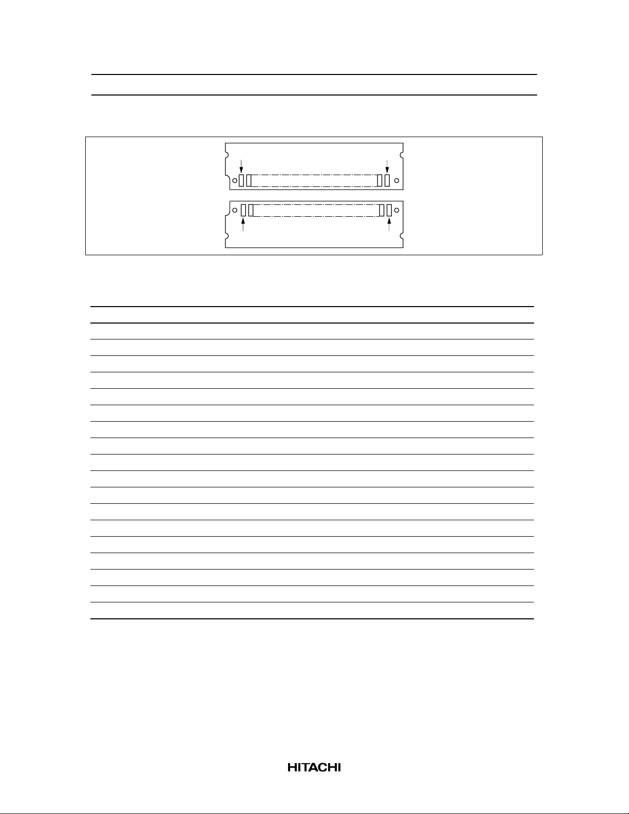
Pin Arrangement
HB56TW432D Series, HB56TW433D Series
1 pin 71 pin
Front side
Back side
72 pin2 pin
Pin Arrangement
Front side Back side
Pin No. Pin name Pin No. Pin name Pin No. Pin name Pin No. Pin name
1V
SS
3 DQ1 39 V
5 DQ3 41 CE2 6 DQ4 42 CE3
7 DQ5 43 CE1 8 DQ6 44 RE0
9 DQ7 45 NC 10 V
11 PD1 47 WE 12 A0 48 NC
13 A1 49 DQ20 14 A2 50 DQ21
15 A3 51 DQ22 16 A4 52 DQ23
17 A5 53 DQ24 18 A6 54 DQ25
19 A10 55 NC 20 NC 56 DQ27
21 DQ9 57 DQ28 22 DQ10 58 DQ29
23 DQ11 59 DQ31 24 DQ12 60 DQ30
25 DQ13 61 V
27 DQ15 63 DQ33 28 A7 64 DQ34
29 A11 (NC)*
31 A8 67 PD3 32 A9 68 PD4
33 NC 69 PD5 34 RE2 70 PD6
35 DQ16 71 PD7 36 NC 72 V
Note: 1. A11: HB56TW432D, NC: HB56TW433D
37 DQ18 2 DQ0 38 DQ19
SS
CC
1
65 NC 30 V
4 DQ2 40 CE0
CC
46 NC
26 DQ14 62 DQ32
CC
66 PD2
SS
3
Page 4

HB56TW432D Series, HB56TW433D Series
Pin Description
Pin name Function
A0 to A11 (HB56TW432D) Address inputs:
Row address: A0 to A11
Column address: A0 to A9
Refresh address: A0 to A11
A0 to A10 (HB56TW433D) Address inputs:
Row address: A0 to A10
Column address: A0 to A10
Refresh address: A0 to A10
DQ0 to DQ7, DQ9 to DQ16,
DQ18 to DQ25, DQ27 to DQ34
RE0, RE2 Row address strobe (RAS)
CE0 to CE3 column address strobe (CAS)
WE Read/Write enable
V
CC
V
SS
PD1 to PD7 Presence detect
NC No connection
Data-in/Data-out
Power supply
Ground
Presence Detect Pin Arrangement
Function
Pin No. Pin name 50 ns 60 ns 70 ns
11 PD1 NC NC NC
66 PD2 NC NC NC
67 PD3 V
SS
68 PD4 NC NC NC
69 PD5 V
70 PD6 V
SS
SS
71 PD7 NC NC NC
PD7 (L-version) V
SS
V
SS
V
NC V
NC NC
V
SS
V
SS
SS
SS
4
Page 5
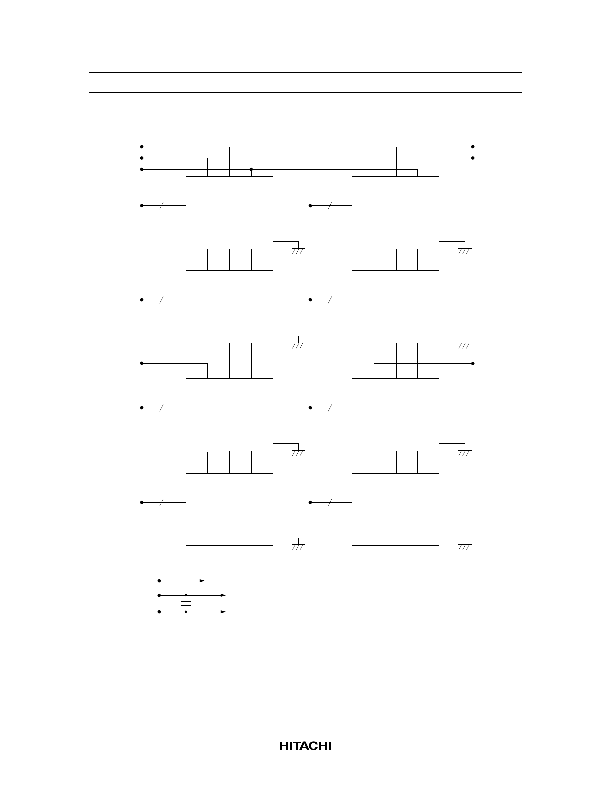
Block Diagram
2
3
2
HB56TW432D Series, HB56TW433D Series
RE0
CE0
WE
DQ0
to
DQ3
DQ4
to
DQ7
CE1
DQ9
to
DQ12
RE
CE
CAS RAS WE
4
I/O1 to I/O4
D0
DQ18
to
DQ21
4
OE
CAS RAS WE
4
I/O1 to I/O4 I/O1 to I/O4
D1
DQ22
to
DQ25
4
OE
CAS RAS WE
I/O1 to I/O4
D4
CAS RAS WE
D5
OE
OE
CE
CAS RAS WE
4
I/O1 to I/O4 I/O1 to I/O4
D2
DQ27
to
DQ30
4
CAS RAS WE
D6
DQ13
to
DQ16
A0 to An
V
V
CC
SS
OE
CAS RAS WE
4
I/O1 to I/O4
D3
DQ31
to
DQ34
4
OE
D0 to D7
D0 to D7
Note: D0 to D7: HM51W16400 (HB56TW432D)
HM51W17400 (HB56TW433D)
CAS RAS WE
I/O1 to I/O4
D7
OE
OE
0.22 µF × 8 pcs
D0 to D7
5
Page 6

HB56TW432D Series, HB56TW433D Series
Absolute Maximum Ratings
Parameter Symbol Value Unit
Voltage on any pin relative to V
Supply voltage relative to V
SS
SS
V
T
V
CC
Short circuit output current Iout 50 mA
Power dissipation Pt 8 W
Operating temperature Topr 0 to +70 °C
Storage temperature Tstg –55 to +125 °C
Recommended DC Operating Conditions (Ta = 0 to 70°C)
Parameter Symbol Min Typ Max Unit Note
Supply voltage V
Input high voltage V
Input low voltage V
Note: 1. All voltage referred to VSS.
SS
VCC3.0 3.3 3.6 V 1
IH
IL
000 V
2.0 — VCC +0.3 V 1
–0.3 — 0.8 V 1
–0.5 to +4.6 V
–0.5 to +4.6 V
6
Page 7

HB56TW432D Series, HB56TW433D Series
DC Characteristics (Ta = 0 to 70°C, VCC = 3.3 V ± 0.3V, VSS = 0 V) (HB56TW432D)
50 ns 60 ns 70 ns
Parameter Symbol Min Max Min Max Min Max Unit Test conditions Notes
Operating current I
Standby current I
Standby current
I
CC1
CC2
CC2
(L-version)
RAS-only refresh
I
CC3
current
Standby current I
CAS-before-RAS
I
CC5
CC6
refresh current
Fast page mode
I
CC7
current
Battery backup current
I
CC10
(Standby with CBR
refresh) (L-version)
Self refresh mode
I
CC11
current (L-version)
Input leakage current I
Output leakage current I
Output high voltage V
Output low voltage V
LI
LO
OH
OL
Notes: 1. ICC depends on output load condition when the device is selected, ICC max is specified at the
output open condition.
2. Address can be changed once or less while RAS = V
3. Address can be changed once or less while CAS = V
— 720 — 640 — 560 mA tRC = min 1, 2
— 16 — 16 — 16 mA TTL interface
RAS, CAS = V
IH
Dout = High-Z
— 8 — 8 — 8 mA CMOS interface
RAS, CAS ≥ V
– 0.2 V
CC
Dout = High-Z
— 0.8 — 0.8 — 0.8 mA CMOS interface
RAS, CAS ≥ V
– 0.2 V
CC
Dout = High-Z
— 720 — 640 — 560 mA tRC = min 2
—40—40—40mARAS = VIH, CAS = V
1
IL
Dout = enable
— 720 — 640 — 560 mA tRC = min
— 640 — 560 — 480 mA tPC = min 1, 3
— 2.4 — 2.4 — 2.4 mA CMOS interface
Dout = High-Z
CBR refresh:
t
= 31.3 µs
RC
t
≤ 0.3 µs
RAS
— 1.6 — 1.6 — 1.6 mA CMOS interface
RAS, CAS ≤ 0.2 V
Dout = High-Z
–10 10 –10 10 –10 10 µA 0 V ≤ Vin ≤ 4.6 V
–10 10 –10 10 –10 10 µA 0 V ≤ Vout ≤ 4.6 V
Dout = disable
2.4 VCC2.4 VCC2.4 VCCV High Iout = –2 mA
0 0.4 0 0.4 0 0.4 V Low Iout = 2 mA
.
IL
.
IH
7
Page 8

HB56TW432D Series, HB56TW433D Series
DC Characteristics (Ta = 0 to 70°C, VCC = 3.3 V ± 0.3V, VSS = 0 V) (HB56TW433D)
50 ns 60 ns 70 ns
Parameter Symbol Min Max Min Max Min Max Unit Test conditions Notes
Operating current I
Standby current I
Standby current
I
CC1
CC2
CC2
(L-version)
RAS-only refresh
I
CC3
current
Standby current I
CAS-before-RAS
I
CC5
CC6
refresh current
Fast page mode
I
CC7
current
Battery backup current
I
CC10
(Standby with CBR
refresh) (L-version)
Self refresh mode
I
CC11
current (L-version)
Input leakage current I
Output leakage current I
Output high voltage V
Output low voltage V
LI
LO
OH
OL
Notes: 1. ICC depends on output load condition when the device is selected, ICC max is specified at the
output open condition.
2. Address can be changed once or less while RAS = V
3. Address can be changed once or less while CAS = V
— 800 — 720 — 640 mA tRC = min 1, 2
— 16 — 16 — 16 mA TTL interface
RAS, CAS = V
IH
Dout = High-Z
— 8 — 8 — 8 mA CMOS interface
RAS, CAS ≥ V
– 0.2 V
CC
Dout = High-Z
— 0.8 — 0.8 — 0.8 mA CMOS interface
RAS, CAS ≥ V
– 0.2 V
CC
Dout = High-Z
— 800 — 720 — 640 mA tRC = min 2
—40—40—40mARAS = VIH, CAS = V
1
IL
Dout = enable
— 800 — 720 — 640 mA tRC = min
— 720 — 640 — 560 mA tPC = min 1, 3
— 2.4 — 2.4 — 2.4 mA CMOS interface
Dout = High-Z
CBR refresh:
t
= 62.5 µs
RC
t
≤ 0.3 µs
RAS
— 1.6 — 1.6 — 1.6 mA CMOS interface
RAS, CAS ≤ 0.2 V
Dout = High-Z
–10 10 –10 10 –10 10 µA 0 V ≤ Vin ≤ 4.6 V
–10 10 –10 10 –10 10 µA 0 V ≤ Vout ≤ 4.6 V
Dout = disable
2.4 VCC2.4 VCC2.4 VCCV High Iout = –2 mA
0 0.4 0 0.4 0 0.4 V Low Iout = 2 mA
.
IL
.
IH
8
Page 9

HB56TW432D Series, HB56TW433D Series
Capacitance (Ta = 25°C, VCC = 3.3 V ± 0.3 V)
Parameter Symbol Typ Max Unit Notes
Input capacitance (Address) C
Input capacitance (WE)C
Input capacitance (CAS)C
Input capacitance (RAS)C
I/O capacitance (DQ) C
I!
I2
I3
I4
I/O
Notes: 1. Capacitance measured with Boonton Meter or effective capacitance measuring method.
2. CAS = V
to disable Dout.
IH
—68pF1
—76pF1
—29pF1
—43pF1
— 17 pF 1, 2
AC Characteristics (Ta = 0 to 70˚C, VCC = 3.3 V ± 0.3 V, VSS = 0 V) *1, *2, *
Test Conditions
• Input rise and fall times: 5 ns
• Input levels: 0 V, 3.0 V
• Input timing reference levels: 0.8 V, 2.0 V
• Output timing reference levels: 0.8 V, 2.0 V
• Output load: 1 TTL gate + CL (100 pF) (Including scope and jig)
17
9
Page 10

HB56TW432D Series, HB56TW433D Series
Read, Write, and Refresh Cycles (Common parameters)
50 ns 60 ns 70 ns
Parameter Symbol Min Max Min Max Min Max Unit Notes
Random read or write cycle
time
RAS precharge time t
CAS precharge time t
RAS pulse width t
CAS pulse width t
Row address setup time t
Row address hold time t
Column address setup time t
Column address hold time t
RAS to CAS delay time t
RAS to column address
delay time
RAS hold time t
CAS hold time t
CAS to RAS precharge time t
CAS delay time from Din t
Transition time (rise and fall) t
Refresh period
( HB 5 6 TW4 32 D: 4 ,0 9 6 cycl e s)
Refresh period
( HB 5 6 TW4 32 D: 4 ,0 9 6 cycl e s)
(L-version)
Refresh period
( HB 5 6 TW4 33 D: 2 ,0 4 8 cycl e s)
Refresh period
( HB 5 6 TW4 33 D: 2 ,0 4 8 cycl e s)
(L-version)
t
t
t
t
t
t
RC
RP
CP
RAS
CAS
ASR
RAH
ASC
CAH
RCD
RAD
RSH
CSH
CRP
DZC
T
REF
REF
REF
REF
90 — 110 — 130 — ns
30 — 40 — 50 — ns
8 — 10 — 10 — ns
50 10000 60 10000 70 10000 ns
13 10000 15 10000 18 10000 ns
0—0—0—ns
8 — 10 — 10 — ns
0—0—0—ns
8 — 10 — 15 — ns
18 37 20 45 20 52 ns 3
13 25 15 30 15 35 ns 4
13 — 15 — 18 — ns
50 — 60 — 70 — ns
5—5—5—ns
0—0—0—ns
350350350ns5
—64—64—64ms
— 128 — 128 — 128 ms
—32—32—32ms
— 128 — 128 — 128 ms
10
Page 11

HB56TW432D Series, HB56TW433D Series
Read Cycle
50 ns 60 ns 70 ns
Parameter Symbol Min Max Min Max Min Max Unit Notes
Access time from RAS t
Access time from CAS t
Access time from address t
Read command setup time t
Read command hold time to
CAS
Read command hold time to
RAS
Column address to RAS lead
time
Column address to CAS lead
time
CAS to output in low-Z t
Output data hold time t
Output buffer turn-off time t
CAS to Din delay time t
t
t
t
t
RAC
CAC
AA
RCS
RCH
RRH
RAL
CAL
CLZ
OH
OFF
CDD
— 50 — 60 — 70 ns 6, 7
— 13 — 15 — 18 ns 7, 8, 15
— 25 — 30 — 35 ns 7, 9, 15
0—0—0—ns
0—0—0—ns10
5—5—5—ns10
25 — 30 — 35 — ns
25 — 30 — 35 — ns
0—0—0—ns
3—3—3—ns
—13—15—15ns11
13 — 15 — 18 — ns
Write Cycle
50 ns 60 ns 70 ns
Parameter Symbol Min Max Min Max Min Max Unit Notes
Write command setup time t
Write command hold time t
Write command pulse width t
Data-in setup time t
Data-in hold time t
WCS
WCH
WP
DS
DH
0—0—0—ns12
8 — 10 — 15 — ns
8 — 10 — 10 — ns
0—0—0—ns13
8 — 10 — 15 — ns 13
11
Page 12

HB56TW432D Series, HB56TW433D Series
Refresh Cycle
50 ns 60 ns 70 ns
Parameter Symbol Min Max Min Max Min Max Unit Notes
CAS setup time
(CBR refresh cycle)
CAS hold time
(CBR refresh cycle)
WE setup time
(CBR refresh cycle)
WE hold time
(CBR refresh cycle)
RAS precharge to CAS hold
time
Fast Page Mode Cycle
Parameter Symbol Min Max Min Max Min Max Unit Notes
Fast page mode cycle time t
Fast page mode RAS pulse
width
Access time from CAS
precharge
RAS hold time from CAS
precharge
t
CSR
t
CHR
t
WRP
t
WRH
t
RPC
PC
t
RASP
t
CPA
t
CPRH
5—5—5—ns
8 — 10 — 10 — ns
0—0—0—ns
8 — 10 — 10 — ns
5—5—5—ns
50 ns 60 ns 70 ns
35 — 40 — 45 — ns
— 100000 — 100000 — 100000 ns 14
— 30 — 35 — 40 ns 7, 15
30 — 35 — 40 — ns
Self Refresh Mode (L-version)
50 ns 60 ns 70 ns
Parameter Symbol Min Max Min Max Min Max Unit Notes
RAS pulse width
(Self refresh)
RAS precharge time
(Self refresh)
CAS hold time (Self refresh) t
12
t
RASS
t
RPS
CHS
100 — 100 — 100 — µs
90 — 110 — 130 — ns
–50 — –50 — –50 — ns
Page 13

HB56TW432D Series, HB56TW433D Series
Notes: 1. AC measurements assume tT = 5 ns.
2. An initial pause of 200 µs is required after power up followed by a minimum of eight initialization
cycles (any combination of cycles containing RAS-only refresh cycle or CAS -before-RAS
refresh). If the internal refresh counter is used, a minimum of eight CAS -before-RAS refresh
cycles are required.
3. Operation with the t
reference point only; if t
controlled exclusively by t
4. Operation with the t
reference point only; if t
controlled exclusively by t
5. V
(min) and VIL (max) are reference levels for measuring timing of input signals. Also, transition
IH
times are measured between V
6. Assumes that t
recommended value shown in this table, t
7. Measured with a load circuit equivalent to 1 TTL loads and 100 pF.
8. Assumes that t
9. Assumes that t
10.Either t
11.t
OFF
or t
RCH
RRH
(max) defines the time at which the outputs achieve the open circuit condition and are not
referred to output voltage levels.
12.Early write cycle only (t
13.These parameters are referred to CAS leading edge in early write cycles.
14.t
defines RAS pulse width in Fast page mode cycles.
RASP
15.Access time is determined by the longest among t
16.When output buffers are enabled once, sustain the low impedance state until valid data is
obtained. When output buffer is turned on and off within a very short time, generally it causes
large V
17.All the V
/ VSS line noise, which causes to degrade VIH min./ VIL max level.
CC
and VSS pins shall be supplied with the same voltages.
CC
18.Please do not use t
transition state from normal operation mode to self refresh mode. If t
precharge time should use t
19.If you use distributed CBR refresh mode with 15.6 µs interval in normal read/write cycle, CBR
refresh should be executed within 15.6 µs immediately after exiting from and before entering into
self refresh mode.
20.If you use RAS only refresh or CBR burst refresh mode in normal read/write cycle, 4096 or 2048
cycles (4096 cycles: HB56TW432D Series, 2048 cycles: HB56TW433D Series) of distributed
CBR refresh with 15.6 µs interval should be executed within 64 or 32 ms (64 ms: HB56TW432D
Series, 32 ms: HB56TW433D Series) immediately after exiting from and before entering into the
self refresh mode.
21.Repetitive self refresh mode without refreshing all memory is not allowed. Once you exit from
self fresh mode, all memory cells need to be refreshed before re-entering the self refresh mode
again.
22.XXX: H or L (H: V
///////: Invalid Dout
When the address, clock and input pins are not described on timing waveforms, their pins must
be applied V
or VIL.
IH
(max) limit insures that t
RCD
is greater than the specified t
RCD
.
CAC
(max) limit insures that t
RAD
is greater than the specified t
RAD
.
AA
(min) and VIL (max).
IH
≤ t
≥ t
≥ t
RCD
RCD
RAD
(max) and t
(max) and t
(max) and t
RCD
RCD
RAD
must be satisfied for a read cycles.
≥ t
WCS
timing, 10 µs ≤ t
RASS
(min) ≤ VIN ≤ VIH (max), L: VIL (min) ≤ VIN ≤ VIL (max))
IH
(min)).
WCS
instead of tRP.
RPS
RAD
RCD
RCD
(max) can be met, t
RAC
(max) can be met, t
RAC
≤ t
(max). If t
RAD
exceeds the value shown.
RAC
+ t
(max) ≥ t
CAC
+ t
(max) ≤ t
CAC
AA
≤ 100 µs. During this period, the device is in
RASS
(max) limit, then access time is
RCD
(max) limit, then access time is
RAD
or t
RCD
+ tAA (max).
RAD
+ tAA (max).
RAD
, t
and t
CAC
is greater than the maximum
RAD
.
CPA
(max) is specified as a
RCD
(max) is specified as a
RAD
≥ 100 µs, then RAS
RASS
13
Page 14
HB56TW432D Series, HB56TW433D Series
Timing Waveforms*
Read Cycle
RAS
CAS
t
ASR
Address
22
t
CSH
t
RCD
t
T
t
RAD
t
t
RAH
ASCtCAH
Row Column
t
RC
t
RAS
t
t
t
t
RSH
CAS
RAL
CAL
t
CRP
t
RP
WE
Din
Dout
t
RCS
t
RAC
t
DZC
t
AA
t
t
CAC
CLZ
High-Z
Dout
t
t
OFF
OH
t
t
CDD
RCH
t
RRH
14
Page 15

Early Write Cycle
RAS
HB56TW432D Series, HB56TW433D Series
t
RC
t
RAS
t
RP
CAS
Address
WE
t
T
t
ASRtRAH
t
RCD
t
ASCtCAH
t
WCS
t
DS
t
CSH
t
RSH
t
CAS
t
CRP
ColumnRow
t
WP
t
WCH
t
DH
Din
Dout
Din
High-Z*
t
WCS WCS
*
(min)
t
15
Page 16

HB56TW432D Series, HB56TW433D Series
RAS-Only Refresh Cycle
t
RC
t
RAS
RAS
t
T
t
CRP
CAS
t
ASR
t
RAH
t
RPC
t
RP
t
CRP
Address
Dout
t
OFF
Row
High-Z
16
Page 17

CAS-Before-RAS Refresh Cycle
RAS
HB56TW432D Series, HB56TW433D Series
t
RC
t
RP
t
RAS
t
RP
CAS
WE
Address
Dout
t
t
RPC
CP
t
OFF
t
CSR
t
t
T
WRP
t
t
WRH
CHR
t
High-Z
CP
t
RPCtCRP
17
Page 18

HB56TW432D Series, HB56TW433D Series
Hidden Refresh Cycle
RAS
CAS
Address
WE
t
ASR
t
RC
t
RAS
t
T
t
RSH
t
RCD
t
RAH
t
RAD
t
ASC
t
RAL
t
CAH
t
RP
t
RAS
t
RC
t
RP
t
RAS
t
CHR
t
RC
t
RP
t
CRP
ColumnRow
t
t
RCS
t
RRH
WRP
t
WRH
t
WRP
t
WRH
Din
Dout
t
RAC
t
DZC
t
CDD
High-Z
t
CAC
t
AA
t
OFF
t
CLZ
t
OH
Dout
18
Page 19

Fast Page Mode Read Cycle
,
RAS
t
T
t
CAS
t
RAD
t
ASRtRAH
RCD
t
t
ASC
HB56TW432D Series, HB56TW433D Series
CSH
t
CAS
t
CAL
t
CAH CAH
t
t
CP
t
RASP
ASC
t
CPRH
t
PC
t
CAS
t
CAL
t
CP
tt
t
t
RSH
t
t
RAL
t
CAL
CAHASC
CAS
t
RP
t
CRP
Address
WE
Din
Dout
Row
Column 1 Column 2 Column N
tt
RCS
t
DZC
t
RAC
t
t
t
AA
CAC
CLZ
RCH
t
CDD
tt t
RCS RCS
t
RCH
t
DZC
t
t
OHtAA
t
OFF
CPA
High-ZHigh-Z
t
CAC
t
CLZ
t
CDD
t
t
OH
DZC
t
OFF
t
CPA
t
AA
t
CAC
t
CLZ
High-Z
RRH
t
RCH
t
t
OH
CDD
t
OFF
Dout NDout 2Dout 1
19
Page 20

HB56TW432D Series, HB56TW433D Series
Fast Page Mode Early Write Cycle
RAS
CAS
Address
WE
t
RASP
t
T
t
ASRtRAH
t
RCD
t
t
CSH
t
CAS
ASCtCAH
t
PC
t
CP
t
ASCtCAH
t
CAS
t
CP
t
ASCtCAH
Row Column 1 Column 2 Column N
ttt
t
WCS
t
WCH
t
WCS
t
WCH
t
WCS
t
RP
t
RSH
t
CAS
WPWPWP
t
WCH
t
CRP
20
Din
Dout
t
t
DS
DH
t
t
DS
DH
t
Din 1 Din 2 Din N
High-Z*
DS
*
t
DH
t
t
WCS WCS
(min)
Page 21

HB56TW432D Series, HB56TW433D Series
Self Refresh Cycle (L-version)*
t
RP
RAS
t
t
CSR
WRPtWRH
CAS
WE
Dout
t
RPC
t
CP
t
OFF
18, 19, 20, 21
T
t
RASS
t
CHS
t
RPS
t
CRP
t
High-Z
21
Page 22

HB56TW432D Series, HB56TW433D Series
Physical Outline
Unit :
mm
inch
Front side
2 – R3.00 min
2 – R0.118 min
Back side
2 – R2.00 ± 0.10
2 – R0.079 ± 0.004
5.00
0.197
R2.00
R0.079
3.18
0.125
7.62
0.300
2.00
0.079
8.25
0.325
2 – Ø1.80
2 – Ø0.071
59.69
2.350
51.66
2.034
Component area
(front)
1
44.45
1.750
44.45
1.750
272
Component area
(back)
71
A
3.00 min
0.118 min
3.00 min
0.118 min
1.80
0.071
17.78
0.700
25.40
1.000
3.18 min
0.125 min
3.80 max
0.150 max
3.18 min
0.125 min
1.00 ± 0.10
0.039 ± 0.004
22
Detail A
2.54 min
0.100 min
1.00±0.05
0.039±0.002
0.25 max
0.010 max
1.27 typ
0.050 typ
Page 23

HB56TW432D Series, HB56TW433D Series
When using this document, keep the following in mind:
1. This document may, wholly or partially, be subject to change without notice.
2. All rights are reserved: No one is permitted to reproduce or duplicate, in any form, the whole or part of
this document without Hitachi’s permission.
3. Hitachi will not be held responsible for any damage to the user that may result from accidents or any
other reasons during operation of the user’s unit according to this document.
4. Circuitry and other examples described herein are meant merely to indicate the characteristics and
performance of Hitachi’s semiconductor products. Hitachi assumes no responsibility for any intellectual
property claims or other problems that may result from applications based on the examples described
herein.
5. No license is granted by implication or otherwise under any patents or other rights of any third party or
Hitachi, Ltd.
6. MEDICAL APPLICATIONS: Hitachi’s products are not authorized for use in MEDICAL
APPLICATIONS without the written consent of the appropriate officer of Hitachi’s sales company.
Such use includes, but is not limited to, use in life support systems. Buyers of Hitachi’s products are
requested to notify the relevant Hitachi sales offices when planning to use the products in MEDICAL
APPLICATIONS.
Hitachi, Ltd.
Semiconductor & IC Div.
Nippon Bldg., 2-6-2, Ohte-machi, Chiyoda-ku, Tokyo 100, Japan
Tel: Tokyo (03) 3270-2111
Fax: (03) 3270-5109
For further information write to:
Hitachi America, Ltd.
Semiconductor & IC Div.
2000 Sierra Point Parkway
Brisbane, CA. 94005-1835
U S A
Tel: 415-589-8300
Fax: 415-583-4207
Hitachi Europe GmbH
Electronic Components Group
Continental Europe
Dornacher Straße 3
D-85622 Feldkirchen
München
Tel: 089-9 91 80-0
Fax: 089-9 29 30 00
Hitachi Europe Ltd.
Electronic Components Div.
Northern Europe Headquarters
Whitebrook Park
Lower Cookham Road
Maidenhead
Berkshire SL6 8YA
United Kingdom
Tel: 0628-585000
Fax: 0628-778322
Hitachi Asia Pte. Ltd.
16 Collyer Quay #20-00
Hitachi Tower
Singapore 0104
Tel: 535-2100
Fax: 535-1533
Hitachi Asia (Hong Kong) Ltd.
Unit 706, North Tower,
World Finance Centre,
Harbour City, Canton Road
Tsim Sha Tsui, Kowloon
Hong Kong
Tel: 27359218
Fax: 27306071
23
Page 24

HB56TW432D Series, HB56TW433D Series
Revision Record
Rev. Date Contents of Modification Drawn by Approved by
1.0 Feb. 27, 1997 Initial issue
24
 Loading...