

Page 1

H8S/2345 Series
H8S/2345, H8S/2344, H8S/2343,
H8S/2341, H8S/2340
TM
H8S/2345 F-ZTAT
Hardware Manual
ADE-602-129A
Rev. 2.0
1/12/98
Hitachi, Ltd.
Page 2

Cautions
1. Hitachi neither warrants nor grants licenses of any rights of Hitachi’s or any third party’s
patent, copyright, trademark, or other intellectual property rights for information contained in
this document. Hitachi bears no responsibility for problems that may arise with third party’s
rights, including intellectual property rights, in connection with use of the information
contained in this document.
2. Products and product specifications may be subject to change without notice. Confirm that you
have received the latest product standards or specifications before final design, purchase or
use.
3. Hitachi makes every attempt to ensure that its products are of high quality and reliability.
However, contact Hitachi’s sales office before using the product in an application that
demands especially high quality and reliability or where its failure or malfunction may directly
threaten human life or cause risk of bodily injury, such as aerospace, aeronautics, nuclear
power, combustion control, transportation, traffic, safety equipment or medical equipment for
life support.
4. Design your application so that the product is used within the ranges guaranteed by Hitachi
particularly for maximum rating, operating supply voltage range, heat radiation characteristics,
installation conditions and other characteristics. Hitachi bears no responsibility for failure or
damage when used beyond the guaranteed ranges. Even within the guaranteed ranges,
consider normally foreseeable failure rates or failure modes in semiconductor devices and
employ systemic measures such as fail-safes, so that the equipment incorporating Hitachi
product does not cause bodily injury, fire or other consequential damage due to operation of
the Hitachi product.
5. This product is not designed to be radiation resistant.
6. No one is permitted to reproduce or duplicate, in any form, the whole or part of this document
without written approval from Hitachi.
7. Contact Hitachi’s sales office for any questions regarding this document or Hitachi
semiconductor products.
Page 3

Main Amendments and Additions in this Edition
Page Item Revision
Throughout • H8S/2344, H8S/2341, and H8S/2340 added; F-ZTAT version of current H8S/2345
added. Generic name adopted: H8S/2345 Series, H8S/2345 F-ZTAT Hardware
Manual.
• Notes added where necessary indicating that the H8S/2340 is a ROMless version,
and only supports MCU operating modes 1, 4, and 5.
• Notes added where necessary indicating that the H8S/2345 F-ZTAT version only
supports MCU operating modes 4 to 7, 10, 11, 14, and 15 (and that modes 1 to 3
(normal modes) cannot be used).
• Notes added where necessary indicating that the FWE pin applies only to the FZTAT version, and that this pin is WDTOVF in the ZTAT, mask ROM, and ROMless
versions.
• Notes added where necessary indicating that the TFP-100G package is under
development.
1 to 5 1.1 Overview Amended (Information on newly added
products)
9 to 13 Table 1.2 Pin Functions in Each
Operating Mode
14 to 20 Table 1.3 Pin Functions Amended
69 to 72 3.1 Overview Amended (Description of F-ZTAT and
74 System Control Register 2 (SYSCR2) (F-
ZTAT Version Only)
76 3.3.7 Mode 7 Note 2 amended
76, 77 3.3.8 Mode 8 to 3.3.13 Mode 15 New
78 Table 3.3 Pin Functions in Each Mode Amended (Mode 10, 11, 14, and 15 pin
Amended
• PROM mode pin names partially
changed
• Flash memory mode pin names added
• Addition of F-ZTAT version operating
mode settings by pins MD2-MD0
• FWE pin description added
ROMless versions added)
New
descriptions added)
79 to 90 3.5 Memory Map in Each Operating Mode Amended (Information on newly added
products)
107 Table 5.3 Correspondence between
Interrupt Sources and IPR Settings
141 6.2.5 Bus Control Register L (BCRL) Description of bit 5 amended
Note amended
Page 4

Page Item Revision
160 Figure 6.14 Example of Wait Insertion
Timing
273 8.12.2 Register Configuration, Port G
Data Direction Register (PGDDR)
294 to 309 9.2.3 Timer I/O Control Register (TIOR) Amended (Register name added to tables)
420 12.2.5 Serial Mode Register (SMR) Description of bit 3 amended
429 to 431 Table 12.3 BRR Settings for Various Bit
Rates (Asynchronous Mode)
441 Figure 12.2 Data Format in Asynchronous
Communication (Example with 8-Bit Data,
Parity, Two Stop Bits)
461 Figure 12.15 Sample SCI Initialization
Flowchart
467 Figure 12.20 Sample Flowchart of
Simultaneous Serial Transmit and Receive
Operations
478, 479 13.2.2 Serial Status Register (SSR) Description of bits 4 and 2 amended
481 13.2.4 Serial Control Register (SCR) Description of bits 1 and 0 amended
483 Figure 13.2 Schematic Diagram of Smart
Card Interface Pin Connections
484 Figure 13.3 Smart Card Interface Data
Format
488, 489 Table 13.5 Examples of Bit Rate B (bit/s)
for Various BRR Settings (When n = 0)
Table 13.6 Examples of BRR Settings for
Bit Rate B (bit/s) (When n = 0)
491 to 493 13.3.6 Data Transfer Operations, Serial
Data Transmission
497, 498 13.3.7 Operation in GSM Mode Amended (Old section 13.3.7, Example of
510 14.2.3 A/D Control Register (ADCR) Description of bits 7 and 6 amended
519 to 524 14.6 Usage Notes (1) Amendment of setting range for analog
529 15.2.2 D/A Control Register (DACR) Bit 5 description amended
532 15.4 Usage Notes New
Amended
Description amended
Amendments to some Error column
entries (values not entered for error of 3%
or above)
Amended
Note added
Note amended
Amended
Amended
Amended (ø = 20.00 MHz column added)
Amended
Use in Software Standby Mode, replaced
with new section)
power supply pins etc.
(2) Deletion of module stop mode
interrupts
Page 5

Page Item Revision
533 16.1 Overview Description amended (Information on
newly added products)
534 Figure 16.1 Block Diagram of RAM
Title of figure amended
(H8S/2345, Advanced Mode)
535 16.3 Operation Description amended (Information on
newly added products)
Whole of
section 17
Whole of
section 20
Section 17 ROM
New flash memory description added, complete revision of section contents and layout
Section 20 Electrical Characteristics
Previous text used as electrical characteristics for ZTAT, mask ROM, and ROMless
versions; new F-ZTAT version electrical characteristics added.
"Preliminary" notation deleted and "TBD" replaced with values for ZTAT, mask ROM,
and ROMless versions.
666 Figure 20.9 Reset Input Timing Amended
669 Figure 20.12 Basic Bus Timing (Three-
State Access)
675 Figure 20.24 SCK Clock Input Timing Amended (t
Amended (t
specification)
WDS
specification)
SCKW
677 to 752 Appendix A Instruction Set Amended (Replaced with latest version)
753 to 759 B.1 Addresses Amended (Addition of registers used by F-
ZTAT version)
760 to 858 B.2 Functions Amended
• Addition of registers used by F-ZTAT
version
• Amendment of note on interrupt priority
registers A-K
893 Table F.1 H8S/2345 Series Product Code
Lineup
Amended (Information on newly added
products)
Page 6

Preface
The H8S/2345 Series is a series of high-performance microcontrollers with a 32-bit H8S/2000
CPU core, and a set of on-chip supporting functions required for system configuration.
The H8S/2000 CPU can execute basic instructions in one state, and is provided with sixteen 16-bit
general registers with a 32-bit internal configuration, and a concise and optimized instruction set.
The CPU can handle a 16 Mbyte linear address space (architecturally 4 Gbytes). Programs based
on the high-level language C can also be run efficiently.
The address space is divided into eight areas. The data bus width and access states can be selected
for each of these areas, and various kinds of memory can be connected fast and easily.
1
On-chip memory consists of large-capacity ROM and RAM. With regard to on-chip ROM
single power supply flash memory (F-ZTAT™
2
*
), PROM (ZTAT™
2
*
), and mask ROM versions
are available, providing a quick and flexible response to conditions from ramp-up through fullscale volume production, even for applications with frequently changing specifications.
On-chip supporting functions include a 16-bit timer pulse unit (TPU), 8-bit timers, watchdog timer
(WDT), serial communication interface (SCI), A/D converter, D/A converter, and I/O ports.
An on-chip data transfer controller (DTC) is also provided, enabling high-speed data transfer
without CPU intervention.
*
,
Use of the H8S/2345 Series enables compact, high-performance systems to be implemented easily.
This manual describes the hardware of the H8S/2345 Series. Refer to the H8S/2600 Series and
H8S/2000 Series Programming Manual for a detailed description of the instruction set.
Notes: 1. The H8S/2345, H8S/2344, H8S/2343, and H8S/2341 have on-chip ROM.
The H8S/2340 does not have on-chip ROM.
2. F-ZTAT (Flexible-ZTAT) is a trademark of Hitachi, Ltd.
ZTAT is a trademark of Hitachi, Ltd.
Page 7

Contents
Section 1 Overview........................................................................................................... 1
1.1 Overview............................................................................................................................ 1
1.2 Block Diagram................................................................................................................... 6
1.3 Pin Description.................................................................................................................. 7
1.3.1 Pin Arrangement .................................................................................................. 7
1.3.2 Pin Functions in Each Operating Mode................................................................ 9
1.3.3 Pin Functions........................................................................................................ 14
Section 2 CPU..................................................................................................................... 21
2.1 Overview............................................................................................................................ 21
2.1.1 Features ................................................................................................................ 21
2.1.2 Differences between H8S/2600 CPU and H8S/2000 CPU .................................. 22
2.1.3 Differences from H8/300 CPU............................................................................. 23
2.1.4 Differences from H8/300H CPU.......................................................................... 23
2.2 CPU Operating Modes ...................................................................................................... 24
2.3 Address Space.................................................................................................................... 29
2.4 Register Configuration ......................................................................................................30
2.4.1 Overview.............................................................................................................. 30
2.4.2 General Registers.................................................................................................. 31
2.4.3 Control Registers.................................................................................................. 32
2.4.4 Initial Register Values.......................................................................................... 34
2.5 Data Formats...................................................................................................................... 35
2.5.1 General Register Data Formats ............................................................................ 35
2.5.2 Memory Data Formats.......................................................................................... 37
2.6 Instruction Set.................................................................................................................... 38
2.6.1 Overview.............................................................................................................. 38
2.6.2 Instructions and Addressing Modes ..................................................................... 39
2.6.3 Table of Instructions Classified by Function........................................................ 41
2.6.4 Basic Instruction Formats..................................................................................... 51
2.7 Addressing Modes and Effective Address Calculation..................................................... 52
2.7.1 Addressing Mode.................................................................................................. 52
2.7.2 Effective Address Calculation.............................................................................. 55
2.8 Processing States ............................................................................................................... 59
2.8.1 Overview.............................................................................................................. 59
2.8.2 Reset State............................................................................................................ 60
2.8.3 Exception-Handling State .................................................................................... 61
2.8.4 Program Execution State...................................................................................... 64
2.8.5 Bus-Released State............................................................................................... 64
2.8.6 Power-Down State................................................................................................ 64
i
Page 8

2.9 Basic Timing...................................................................................................................... 65
2.9.1 Overview.............................................................................................................. 65
2.9.2 On-Chip Memory (ROM, RAM) ......................................................................... 65
2.9.3 On-Chip Supporting Module Access Timing....................................................... 67
2.9.4 External Address Space Access Timing............................................................... 68
Section 3 MCU Operating Modes................................................................................ 69
3.1 Overview............................................................................................................................ 69
3.1.1 Operating Mode Selection (F-ZTAT™ Version)................................................. 69
3.1.2 Operating Mode Selection (ZTAT, Mask ROM, and No On-Chip ROM
Versions) .............................................................................................................. 70
3.1.3 Register Configuration ......................................................................................... 72
3.2 Register Descriptions......................................................................................................... 72
3.2.1 Mode Control Register (MDCR).......................................................................... 72
3.2.2 System Control Register (SYSCR) ...................................................................... 73
3.2.3 System Control Register 2 (SYSCR2) (F-ZTAT Version Only) ......................... 74
3.3 Operating Mode Descriptions............................................................................................ 75
3.3.1 Mode 1 (ZTAT, Mask ROM, and No On-Chip ROM Versions Only)................ 75
3.3.2 Mode 2
3.3.3 Mode 3
3.3.4 Mode 4
3.3.5 Mode 5
3.3.6 Mode 6
3.3.7 Mode 7
3.3.8 Modes 8 and 9 (F-ZTAT Version Only) .............................................................. 76
3.3.9 Mode 10 (F-ZTAT Version Only)........................................................................ 77
3.3.10 Mode 11 (F-ZTAT Version Only)........................................................................ 77
3.3.11 Modes 12 and 13 (F-ZTAT Version Only) .......................................................... 77
3.3.12 Mode 14 (F-ZTAT Version Only)........................................................................ 77
3.3.13 Mode 15 (F-ZTAT Version Only)........................................................................ 77
3.4 Pin Functions in Each Operating Mode............................................................................. 78
3.5 Memory Map in Each Operating Mode............................................................................. 79
1
*
(ZTAT and Mask ROM Versions Only).............................................. 75
1
*
(ZTAT and Mask ROM Versions Only).............................................. 75
2
*
.............................................................................................................. 75
2
*
.............................................................................................................. 76
1
*
.............................................................................................................. 76
1
*
.............................................................................................................. 76
Section 4 Exception Handling........................................................................................ 91
4.1 Overview............................................................................................................................ 91
4.1.1 Exception Handling Types and Priority ............................................................... 91
4.1.2 Exception Handling Operation............................................................................. 92
4.1.3 Exception Vector Table........................................................................................ 92
4.2 Reset.................................................................................................................................. 94
4.2.1 Overview.............................................................................................................. 94
4.2.2 Reset Types .......................................................................................................... 94
4.2.3 Reset Sequence..................................................................................................... 95
4.2.4 Interrupts after Reset ............................................................................................ 96
ii
Page 9

4.2.5 State of On-Chip Supporting Modules after Reset Release ................................. 96
4.3 Traces ................................................................................................................................ 97
4.4 Interrupts............................................................................................................................ 98
4.5 Trap Instruction ................................................................................................................. 99
4.6 Stack Status after Exception Handling.............................................................................. 100
4.7 Notes on Use of the Stack.................................................................................................. 101
Section 5 Interrupt Controller........................................................................................ 103
5.1 Overview............................................................................................................................ 103
5.1.1 Features ................................................................................................................ 103
5.1.2 Block Diagram...................................................................................................... 104
5.1.3 Pin Configuration ................................................................................................. 105
5.1.4 Register Configuration ......................................................................................... 105
5.2 Register Descriptions......................................................................................................... 106
5.2.1 System Control Register (SYSCR) ..................................................................... 106
5.2.2 Interrupt Priority Registers A to K (IPRA to IPRK)............................................ 107
5.2.3 IRQ Enable Register (IER) .................................................................................. 108
5.2.4 IRQ Sense Control Registers H and L (ISCRH, ISCRL)..................................... 109
5.2.5 IRQ Status Register (ISR).................................................................................... 110
5.3 Interrupt Sources................................................................................................................ 111
5.3.1 External Interrupts................................................................................................ 111
5.3.2 Internal Interrupts................................................................................................. 112
5.3.3 Interrupt Exception Handling Vector Table......................................................... 112
5.4 Interrupt Operation............................................................................................................ 116
5.4.1 Interrupt Control Modes and Interrupt Operation................................................ 116
5.4.2 Interrupt Control Mode 0...................................................................................... 119
5.4.3 Interrupt Control Mode 2...................................................................................... 121
5.4.4 Interrupt Exception Handling Sequence .............................................................. 123
5.4.5 Interrupt Response Times..................................................................................... 125
5.5 Usage Notes....................................................................................................................... 126
5.5.1 Contention between Interrupt Generation and Disabling..................................... 126
5.5.2 Instructions that Disable Interrupts ...................................................................... 127
5.5.3 Times when Interrupts are Disabled..................................................................... 127
5.5.4 Interrupts during Execution of EEPMOV Instruction.......................................... 127
5.6 DTC Activation by Interrupt ............................................................................................. 128
5.6.1 Overview.............................................................................................................. 128
5.6.2 Block Diagram...................................................................................................... 128
5.6.3 Operation.............................................................................................................. 129
Section 6 Bus Controller.................................................................................................. 131
6.1 Overview............................................................................................................................ 131
6.1.1 Features ................................................................................................................ 131
6.1.2 Block Diagram...................................................................................................... 132
iii
Page 10

6.1.3 Pin Configuration ................................................................................................. 133
6.1.4 Register Configuration ......................................................................................... 133
6.2 Register Descriptions......................................................................................................... 134
6.2.1 Bus Width Control Register (ABWCR)............................................................... 134
6.2.2 Access State Control Register (ASTCR).............................................................. 135
6.2.3 Wait Control Registers H and L (WCRH, WCRL).............................................. 136
6.2.4 Bus Control Register H (BCRH).......................................................................... 139
6.2.5 Bus Control Register L (BCRL)........................................................................... 141
6.3 Overview of Bus Control................................................................................................... 142
6.3.1 Area Partitioning .................................................................................................. 142
6.3.2 Bus Specifications................................................................................................ 144
6.3.3 Memory Interfaces................................................................................................ 145
6.3.4 Advanced Mode.................................................................................................... 145
6.3.5 Areas in Normal Mode (ZTAT, Mask ROM, and No On-Chip ROM
Versions Only)...................................................................................................... 146
6.3.6 Chip Select Signals............................................................................................... 147
6.4 Basic Bus Interface............................................................................................................ 148
6.4.1 Overview.............................................................................................................. 148
6.4.2 Data Size and Data Alignment ............................................................................. 148
6.4.3 Valid Strobes........................................................................................................ 150
6.4.4 Basic Timing ........................................................................................................ 151
6.4.5 Wait Control......................................................................................................... 159
6.5 Burst ROM Interface ......................................................................................................... 161
6.5.1 Overview.............................................................................................................. 161
6.5.2 Basic Timing ........................................................................................................ 161
6.5.3 Wait Control......................................................................................................... 163
6.6 Idle Cycle........................................................................................................................... 164
6.6.1 Operation.............................................................................................................. 164
6.6.2 Pin States in Idle Cycle ........................................................................................ 167
6.7 Bus Release........................................................................................................................ 167
6.7.1 Overview.............................................................................................................. 167
6.7.2 Operation.............................................................................................................. 167
6.7.3 Pin States in External Bus Released State............................................................ 168
6.7.4 Transition Timing................................................................................................. 169
6.7.5 Usage Note ........................................................................................................... 170
6.8 Bus Arbitration.................................................................................................................. 170
6.8.1 Overview.............................................................................................................. 170
6.8.2 Operation.............................................................................................................. 170
6.8.3 Bus Transfer Timing ............................................................................................ 171
6.8.4 External Bus Release Usage Note........................................................................ 171
6.9 Resets and the Bus Controller............................................................................................ 171
iv
Page 11

Section 7 Data Transfer Controller .............................................................................. 173
7.1 Overview............................................................................................................................ 173
7.1.1 Features ................................................................................................................ 173
7.1.2 Block Diagram...................................................................................................... 174
7.1.3 Register Configuration ......................................................................................... 175
7.2 Register Descriptions......................................................................................................... 176
7.2.1 DTC Mode Register A (MRA)............................................................................. 176
7.2.2 DTC Mode Register B (MRB) ............................................................................. 178
7.2.3 DTC Source Address Register (SAR).................................................................. 179
7.2.4 DTC Destination Address Register (DAR).......................................................... 179
7.2.5 DTC Transfer Count Register A (CRA) .............................................................. 179
7.2.6 DTC Transfer Count Register B (CRB) ............................................................... 180
7.2.7 DTC Enable Registers (DTCER) ......................................................................... 180
7.2.8 DTC Vector Register (DTVECR)........................................................................ 181
7.2.9 Module Stop Control Register (MSTPCR) .......................................................... 182
7.3 Operation ........................................................................................................................... 183
7.3.1 Overview.............................................................................................................. 183
7.3.2 Activation Sources................................................................................................ 185
7.3.3 DTC Vector Table................................................................................................ 186
7.3.4 Location of Register Information in Address Space ............................................ 189
7.3.5 Normal Mode........................................................................................................ 190
7.3.6 Repeat Mode ........................................................................................................ 191
7.3.7 Block Transfer Mode............................................................................................ 192
7.3.8 Chain Transfer...................................................................................................... 194
7.3.9 Operation Timing ................................................................................................. 195
7.3.10 Number of DTC Execution States........................................................................ 196
7.3.11 Procedures for Using DTC ................................................................................... 198
7.3.12 Examples of Use of the DTC................................................................................ 199
7.4 Interrupts............................................................................................................................ 201
7.5 Usage Notes....................................................................................................................... 201
Section 8 I/O Ports ............................................................................................................ 203
8.1 Overview............................................................................................................................ 203
8.2 Port 1.................................................................................................................................. 208
8.2.1 Overview.............................................................................................................. 208
8.2.2 Register Configuration ......................................................................................... 209
8.2.3 Pin Functions........................................................................................................ 210
8.3 Port 2.................................................................................................................................. 219
8.3.1 Overview.............................................................................................................. 219
8.3.2 Register Configuration ......................................................................................... 219
8.3.3 Pin Functions........................................................................................................ 221
8.4 Port 3.................................................................................................................................. 230
8.4.1 Overview.............................................................................................................. 230
v
Page 12

8.4.2 Register Configuration ......................................................................................... 230
8.4.3 Pin Functions........................................................................................................ 233
8.5 Port 4.................................................................................................................................. 235
8.5.1 Overview.............................................................................................................. 235
8.5.2 Register Configuration ......................................................................................... 236
8.5.3 Pin Functions........................................................................................................ 236
8.6 Port A................................................................................................................................. 237
8.6.1 Overview.............................................................................................................. 237
8.6.2 Register Configuration ......................................................................................... 238
8.6.3 Pin Functions........................................................................................................ 241
8.6.4 MOS Input Pull-Up Function............................................................................... 242
8.7 Port B................................................................................................................................. 243
8.7.1 Overview.............................................................................................................. 243
8.7.2 Register Configuration ......................................................................................... 244
8.7.3 Pin Functions........................................................................................................ 246
8.7.4 MOS Input Pull-Up Function............................................................................... 248
8.8 Port C................................................................................................................................. 249
8.8.1 Overview.............................................................................................................. 249
8.8.2 Register Configuration ......................................................................................... 250
8.8.3 Pin Functions........................................................................................................ 252
8.8.4 MOS Input Pull-Up Function............................................................................... 254
8.9 Port D................................................................................................................................. 255
8.9.1 Overview.............................................................................................................. 255
8.9.2 Register Configuration ......................................................................................... 256
8.9.3 Pin Functions........................................................................................................ 258
8.9.4 MOS Input Pull-Up Function............................................................................... 259
8.10 Port E................................................................................................................................. 260
8.10.1 Overview.............................................................................................................. 260
8.10.2 Register Configuration ......................................................................................... 261
8.10.3 Pin Functions........................................................................................................ 263
8.10.4 MOS Input Pull-Up Function ............................................................................... 264
8.11 Port F ................................................................................................................................. 265
8.11.1 Overview.............................................................................................................. 265
8.11.2 Register Configuration ......................................................................................... 266
8.11.3 Pin Functions........................................................................................................ 269
8.12 Port G................................................................................................................................. 271
8.12.1 Overview.............................................................................................................. 271
8.12.2 Register Configuration ......................................................................................... 272
8.12.3 Pin Functions........................................................................................................ 275
Section 9 16-Bit Timer Pulse Unit (TPU).................................................................. 277
9.1 Overview............................................................................................................................ 277
9.1.1 Features ................................................................................................................ 277
vi
Page 13

9.1.2 Block Diagram...................................................................................................... 281
9.1.3 Pin Configuration ................................................................................................. 282
9.1.4 Register Configuration ......................................................................................... 284
9.2 Register Descriptions......................................................................................................... 286
9.2.1 Timer Control Register (TCR) ............................................................................. 286
9.2.2 Timer Mode Register (TMDR) ............................................................................ 291
9.2.3 Timer I/O Control Register (TIOR) ..................................................................... 293
9.2.4 Timer Interrupt Enable Register (TIER) .............................................................. 310
9.2.5 Timer Status Register (TSR)................................................................................ 313
9.2.6 Timer Counter (TCNT) ........................................................................................ 316
9.2.7 Timer General Register (TGR) ............................................................................ 317
9.2.8 Timer Start Register (TSTR)................................................................................ 318
9.2.9 Timer Synchro Register (TSYR).......................................................................... 319
9.2.10 Module Stop Control Register (MSTPCR) .......................................................... 320
9.3 Interface to Bus Master...................................................................................................... 321
9.3.1 16-Bit Registers.................................................................................................... 321
9.3.2 8-Bit Registers...................................................................................................... 321
9.4 Operation ........................................................................................................................... 323
9.4.1 Overview.............................................................................................................. 323
9.4.2 Basic Functions .................................................................................................... 324
9.4.3 Synchronous Operation........................................................................................ 330
9.4.4 Buffer Operation .................................................................................................. 332
9.4.5 Cascaded Operation.............................................................................................. 336
9.4.6 PWM Modes ........................................................................................................ 338
9.4.7 Phase Counting Mode .......................................................................................... 343
9.5 Interrupts............................................................................................................................ 349
9.5.1 Interrupt Sources and Priorities............................................................................ 349
9.5.2 DTC Activation.................................................................................................... 351
9.5.3 A/D Converter Activation .................................................................................... 351
9.6 Operation Timing .............................................................................................................. 352
9.6.1 Input/Output Timing ............................................................................................ 352
9.6.2 Interrupt Signal Timing........................................................................................ 356
9.7 Usage Notes....................................................................................................................... 360
Section 10 8-Bit Timers ..................................................................................................... 371
10.1 Overview............................................................................................................................ 371
10.1.1 Features ................................................................................................................ 371
10.1.2 Block Diagram...................................................................................................... 372
10.1.3 Pin Configuration ................................................................................................. 373
10.1.4 Register Configuration ......................................................................................... 373
10.2 Register Descriptions......................................................................................................... 374
10.2.1 Timer Counters 0 and 1 (TCNT0, TCNT1).......................................................... 374
10.2.2 Time Constant Registers A0 and A1 (TCORA0, TCORA1) ............................... 374
vii
Page 14

10.2.3 Time Constant Registers B0 and B1 (TCORB0, TCORB1)................................ 375
10.2.4 Time Control Registers 0 and 1 (TCR0, TCR1) .................................................. 375
10.2.5 Timer Control/Status Registers 0 and 1 (TCSR0, TCSR1).................................. 377
10.2.6 Module Stop Control Register (MSTPCR) .......................................................... 380
10.3 Operation ........................................................................................................................... 381
10.3.1 TCNT Incrementation Timing.............................................................................. 381
10.3.2 Compare Match Timing ....................................................................................... 382
10.3.3 Timing of External RESET on TCNT.................................................................. 384
10.3.4 Timing of Overflow Flag (OVF) Setting.............................................................. 384
10.3.5 Operation with Cascaded Connection .................................................................. 385
10.4 Interrupts............................................................................................................................ 386
10.4.1 Interrupt Sources and DTC Activation................................................................. 386
10.4.2 A/D Converter Activation .................................................................................... 386
10.5 Sample Application ........................................................................................................... 387
10.6 Usage Notes....................................................................................................................... 388
10.6.1 Contention between TCNT Write and Clear........................................................ 388
10.6.2 Contention between TCNT Write and Increment ................................................ 389
10.6.3 Contention between TCOR Write and Compare Match ...................................... 390
10.6.4 Contention between Compare Matches A and B ................................................. 391
10.6.5 Switching of Internal Clocks and TCNT Operation............................................. 391
10.6.6 Usage Note ........................................................................................................... 393
Section 11 Watchdog Timer ............................................................................................. 395
11.1 Overview............................................................................................................................ 395
11.1.1 Features ................................................................................................................ 395
11.1.2 Block Diagram...................................................................................................... 396
11.1.3 Pin Configuration ................................................................................................. 397
11.1.4 Register Configuration ......................................................................................... 397
11.2 Register Descriptions......................................................................................................... 398
11.2.1 Timer Counter (TCNT) ........................................................................................ 398
11.2.2 Timer Control/Status Register (TCSR)................................................................ 398
11.2.3 Reset Control/Status Register (RSTCSR)............................................................ 400
11.2.4 Notes on Register Access ..................................................................................... 402
11.3 Operation ........................................................................................................................... 404
11.3.1 Watchdog Timer Operation.................................................................................. 404
11.3.2 Interval Timer Operation...................................................................................... 406
11.3.3 Timing of Setting Overflow Flag (OVF).............................................................. 406
11.3.4 Timing of Setting of Watchdog Timer Overflow Flag (WOVF) ......................... 407
11.4 Interrupts............................................................................................................................ 408
11.5 Usage Notes....................................................................................................................... 408
11.5.1 Contention between Timer Counter (TCNT) Write and Increment ..................... 408
11.5.2 Changing Value of CKS2 to CKS0...................................................................... 408
11.5.3 Switching between Watchdog Timer Mode and Interval Timer Mode................ 409
viii
Page 15

11.5.4 System Reset by WDTOVF Signal...................................................................... 409
11.5.5 Internal Reset in Watchdog Timer Mode ............................................................. 409
Section 12 Serial Communication Interface (SCI) .................................................... 411
12.1 Overview............................................................................................................................ 411
12.1.1 Features ................................................................................................................ 411
12.1.2 Block Diagram...................................................................................................... 413
12.1.3 Pin Configuration ................................................................................................. 414
12.1.4 Register Configuration ......................................................................................... 415
12.2 Register Descriptions......................................................................................................... 416
12.2.1 Receive Shift Register (RSR)............................................................................... 416
12.2.2 Receive Data Register (RDR) .............................................................................. 416
12.2.3 Transmit Shift Register (TSR).............................................................................. 417
12.2.4 Transmit Data Register (TDR) ............................................................................. 417
12.2.5 Serial Mode Register (SMR)................................................................................ 418
12.2.6 Serial Control Register (SCR).............................................................................. 421
12.2.7 Serial Status Register (SSR)................................................................................. 425
12.2.8 Bit Rate Register (BRR)....................................................................................... 428
12.2.9 Smart Card Mode Register (SCMR) .................................................................... 437
12.2.10 Module Stop Control Register (MSTPCR) .......................................................... 438
12.3 Operation ........................................................................................................................... 439
12.3.1 Overview.............................................................................................................. 439
12.3.2 Operation in Asynchronous Mode........................................................................ 441
12.3.3 Multiprocessor Communication Function............................................................ 452
12.3.4 Operation in Clocked Synchronous Mode ........................................................... 460
12.4 SCI Interrupts .................................................................................................................... 468
12.5 Usage Notes....................................................................................................................... 469
Section 13 Smart Card Interface...................................................................................... 473
13.1 Overview............................................................................................................................ 473
13.1.1 Features ................................................................................................................ 473
13.1.2 Block Diagram...................................................................................................... 474
13.1.3 Pin Configuration ................................................................................................. 475
13.1.4 Register Configuration ......................................................................................... 476
13.2 Register Descriptions......................................................................................................... 477
13.2.1 Smart Card Mode Register (SCMR) .................................................................... 477
13.2.2 Serial Status Register (SSR)................................................................................. 478
13.2.3 Serial Mode Register (SMR)................................................................................ 480
13.2.4 Serial Control Register (SCR).............................................................................. 481
13.3 Operation ........................................................................................................................... 482
13.3.1 Overview.............................................................................................................. 482
13.3.2 Pin Connections.................................................................................................... 482
13.3.3 Data Format.......................................................................................................... 484
ix
Page 16

13.3.4 Register Settings................................................................................................... 486
13.3.5 Clock .................................................................................................................... 488
13.3.6 Data Transfer Operations ..................................................................................... 490
13.3.7 Operation in GSM Mode...................................................................................... 497
13.4 Usage Note ........................................................................................................................ 498
Section 14 A/D Converter ................................................................................................. 503
14.1 Overview............................................................................................................................ 503
14.1.1 Features ................................................................................................................ 503
14.1.2 Block Diagram...................................................................................................... 504
14.1.3 Pin Configuration ................................................................................................. 505
14.1.4 Register Configuration ......................................................................................... 506
14.2 Register Descriptions......................................................................................................... 507
14.2.1 A/D Data Registers A to D (ADDRA to ADDRD).............................................. 507
14.2.2 A/D Control/Status Register (ADCSR)................................................................ 508
14.2.3 A/D Control Register (ADCR)............................................................................. 510
14.2.4 Module Stop Control Register (MSTPCR) .......................................................... 511
14.3 Interface to Bus Master...................................................................................................... 512
14.4 Operation ........................................................................................................................... 513
14.4.1 Single Mode (SCAN = 0)..................................................................................... 513
14.4.2 Scan Mode (SCAN = 1) ....................................................................................... 515
14.4.3 Input Sampling and A/D Conversion Time.......................................................... 517
14.4.4 External Trigger Input Timing ............................................................................. 518
14.5 Interrupts............................................................................................................................ 519
14.6 Usage Notes....................................................................................................................... 519
Section 15 D/A Converter ................................................................................................. 525
15.1 Overview............................................................................................................................ 525
15.1.1 Features ................................................................................................................ 525
15.1.2 Block Diagram...................................................................................................... 526
15.1.3 Pin Configuration ................................................................................................. 527
15.1.4 Register Configuration ......................................................................................... 527
15.2 Register Descriptions......................................................................................................... 528
15.2.1 D/A Data Registers 0 and 1 (DADR0, DADR1).................................................. 528
15.2.2 D/A Control Register (DACR)............................................................................. 528
15.2.3 Module Stop Control Register (MSTPCR) .......................................................... 530
15.3 Operation ........................................................................................................................... 531
15.4 Usage Notes....................................................................................................................... 532
Section 16 RAM ................................................................................................................... 533
16.1 Overview............................................................................................................................ 533
16.1.1 Block Diagram...................................................................................................... 534
16.1.2 Register Configuration ......................................................................................... 534
x
Page 17

16.2 Register Descriptions......................................................................................................... 535
16.2.1 System Control Register (SYSCR) ...................................................................... 535
16.3 Operation ........................................................................................................................... 535
16.4 Usage Note ........................................................................................................................ 535
Section 17 ROM................................................................................................................... 537
17.1 Overview.............................................................................................................................. 537
17.1.1 Block Diagram........................................................................................................ 537
17.1.2 Register Configuration............................................................................................ 538
17.2 Register Descriptions............................................................................................................ 538
17.2.1 Mode Control Register (MDCR)............................................................................ 538
17.2.2 Bus Control Register L (BCRL)............................................................................. 539
17.3 Operation.............................................................................................................................. 539
17.4 PROM Mode ........................................................................................................................ 542
17.4.1 PROM Mode Setting.............................................................................................. 542
17.4.2 Socket Adapter and Memory Map.......................................................................... 542
17.5 Programming........................................................................................................................ 545
17.5.1 Overview ................................................................................................................ 545
17.5.2 Programming and Verification............................................................................... 545
17.5.3 Programming Precautions ...................................................................................... 549
17.5.4 Reliability of Programmed Data............................................................................. 550
17.6 Overview of Flash Memory.................................................................................................. 551
17.6.1 Features................................................................................................................... 551
17.6.2 Block Diagram........................................................................................................ 552
17.6.3 Flash Memory Operating Modes............................................................................ 553
17.6.4 Pin Configuration.................................................................................................... 558
17.6.5 Register Configuration............................................................................................ 559
17.7 Register Descriptions............................................................................................................ 560
17.7.1 Flash Memory Control Register 1 (FLMCR1)....................................................... 560
17.7.2 Flash Memory Control Register 2 (FLMCR2)....................................................... 563
17.7.3 Erase Block Registers 1 and 2 (EBR1, EBR2)....................................................... 564
17.7.4 System Control Register 2 (SYSCR2).................................................................... 565
17.7.5 RAM Emulation Register (RAMER) ..................................................................... 566
17.8 On-Board Programming Modes........................................................................................... 568
17.8.1 Boot Mode.............................................................................................................. 569
17.8.2 User Program Mode................................................................................................ 573
17.9 Programming/Erasing Flash Memory.................................................................................. 575
17.9.1 Program Mode — Preliminary —.......................................................................... 576
17.9.2 Program-Verify Mode — Preliminary — .............................................................. 577
17.9.3 Erase Mode — Preliminary —............................................................................... 579
17.9.4 Erase-Verify Mode — Preliminary — ................................................................... 579
17.10 Flash Memory Protection................................................................................................... 581
17.10.1 Hardware Protection............................................................................................. 581
xi
Page 18

17.10.2 Software Protection.............................................................................................. 581
17.10.3 Error Protection.................................................................................................... 582
17.11 Flash Memory Emulation in RAM..................................................................................... 585
17.11.1 Emulation in RAM ............................................................................................... 585
17.11.2 RAM Overlap ....................................................................................................... 586
17.12 Interrupt Handling when Programming/Erasing Flash Memory........................................ 587
17.13 Flash Memory Writer Mode............................................................................................... 588
17.13.1 Writer Mode Setting............................................................................................. 588
17.13.2 Socket Adapters and Memory Map...................................................................... 589
17.13.3 Writer Mode Operation ........................................................................................ 590
17.13.4 Memory Read Mode............................................................................................. 592
17.13.5 Auto-Program Mode............................................................................................. 596
17.13.6 Auto-Erase Mode.................................................................................................. 598
17.13.7 Status Read Mode................................................................................................. 599
17.13.8 Status Polling........................................................................................................ 601
17.13.9 Writer Mode Transition Time .............................................................................. 602
17.13.10 Notes On Memory Programming ....................................................................... 602
17.14 Flash Memory Programming and Erasing Precautions...................................................... 603
Section 18 Clock Pulse Generator .................................................................................. 609
18.1 Overview............................................................................................................................ 609
18.1.1 Block Diagram...................................................................................................... 609
18.1.2 Register Configuration ......................................................................................... 609
18.2 Register Descriptions......................................................................................................... 610
18.2.1 System Clock Control Register (SCKCR)............................................................ 610
18.3 Oscillator............................................................................................................................ 611
18.3.1 Connecting a Crystal Resonator ........................................................................... 611
18.3.2 External Clock Input ............................................................................................ 613
18.4 Duty Adjustment Circuit.................................................................................................... 615
18.5 Medium-Speed Clock Divider........................................................................................... 615
18.6 Bus Master Clock Selection Circuit .................................................................................. 615
Section 19 Power-Down Modes...................................................................................... 617
19.1 Overview.............................................................................................................................. 617
19.1.1 Register Configuration............................................................................................ 618
19.2 Register Descriptions............................................................................................................ 619
19.2.1 Standby Control Register (SBYCR)....................................................................... 619
19.2.2 System Clock Control Register (SCKCR).............................................................. 620
19.2.3 Module Stop Control Register (MSTPCR) ............................................................ 621
19.3 Medium-Speed Mode........................................................................................................... 622
19.4 Sleep Mode........................................................................................................................... 623
19.5 Module Stop Mode............................................................................................................... 623
19.5.1 Module Stop Mode................................................................................................. 623
xii
Page 19

19.5.2 Usage Notes............................................................................................................ 624
19.6 Software Standby Mode....................................................................................................... 625
19.6.1 Software Standby Mode ......................................................................................... 625
19.6.2 Clearing Software Standby Mode .......................................................................... 625
19.6.3 Setting Oscillation Stabilization Time after Clearing Software Standby Mode..... 626
19.6.4 Software Standby Mode Application Example...................................................... 626
19.6.5 Usage Notes............................................................................................................ 627
19.7 Hardware Standby Mode...................................................................................................... 628
19.7.1 Hardware Standby Mode........................................................................................ 628
19.7.2 Hardware Standby Mode Timing ........................................................................... 628
19.8 ø Clock Output Disabling Function...................................................................................... 629
Section 20 Electrical Characteristics.............................................................................. 631
20.1 Electrical Characteristics of F-ZTAT Version .................................................................. 631
20.1.1 Absolute Maximum Ratings................................................................................. 631
20.1.2 DC Characteristics................................................................................................ 632
20.1.3 AC Characteristics................................................................................................ 639
20.1.4 A/D Conversion Characteristics........................................................................... 646
20.1.5 D/A Conversion Characteristics........................................................................... 647
20.1.6 Flash Memory Characteristics.............................................................................. 648
20.2 Electrical Characteristics of ZTAT, Mask ROM, and No On-chip ROM Versions.......... 650
20.2.1 Absolute Maximum Ratings................................................................................. 650
20.2.2 DC Characteristics................................................................................................ 651
20.2.3 AC Characteristics................................................................................................ 656
20.2.4 A/D Conversion Characteristics........................................................................... 663
20.2.5 D/A Conversion Characteristics........................................................................... 664
20.3 Operation Timing .............................................................................................................. 665
20.3.1 Clock Timing........................................................................................................ 665
20.3.2 Control Signal Timing.......................................................................................... 666
20.3.3 Bus Timing........................................................................................................... 667
20.3.4 Timing for On-Chip Supporting Modules............................................................ 673
20.4 Usage Note ........................................................................................................................ 676
Appendix A Instruction Set.............................................................................................. 677
A.1 Instruction List................................................................................................................... 677
A.2 Instruction Codes............................................................................................................... 701
A.3 Operation Code Map.......................................................................................................... 715
A.4 Number of States Required for Instruction Execution...................................................... 719
A.5 Bus States During Instruction Execution........................................................................... 733
A.6 Condition Code Modification............................................................................................ 747
xiii
Page 20

Appendix B Internal I/O Register.................................................................................. 753
B.1 Addresses........................................................................................................................... 753
B.2 Functions............................................................................................................................ 760
Appendix C I/O Port Block Diagrams.......................................................................... 859
C.1 Port 1 Block Diagram........................................................................................................ 859
C.2 Port 2 Block Diagram........................................................................................................ 863
C.3 Port 3 Block Diagram........................................................................................................ 867
C.4 Port 4 Block Diagram........................................................................................................ 870
C.5 Port A Block Diagram ....................................................................................................... 871
C.6 Port B Block Diagram ....................................................................................................... 872
C.7 Port C Block Diagram ....................................................................................................... 873
C.8 Port D Block Diagram ....................................................................................................... 874
C.9 Port E Block Diagram........................................................................................................ 875
C.10 Port F Block Diagram........................................................................................................ 876
C.11 Port G Block Diagram ....................................................................................................... 884
Appendix D Pin States....................................................................................................... 888
D.1 Port States in Each Mode .................................................................................................. 888
Appendix E Timing of Transition to and Recovery from Hardware
Standby Mode
.............................................................................................. 892
Appendix F Product Code Lineup................................................................................. 893
Appendix G Package Dimensions.................................................................................. 894
xiv
Page 21

Section 1 Overview
1.1 Overview
The H8S/2345 Series is a series of microcomputers (MCUs: microcomputer units), built around
the H8S/2000 CPU, employing Hitachi's proprietary architecture, and equipped with peripheral
functions on-chip.
The H8S/2000 CPU has an internal 32-bit architecture, is provided with sixteen 16-bit general
registers and a concise, optimized instruction set designed for high-speed operation, and can
address a 16-Mbyte linear address space. The instruction set is upward-compatible with H8/300
and H8/300H CPU instructions at the object-code level, facilitating migration from the H8/300,
H8/300L, or H8/300H Series.
On-chip peripheral functions required for system configuration include data transfer controller
(DTC) bus masters, ROM and RAM memory, a16-bit timer-pulse unit (TPU), 8-bit timer,
watchdog timer (WDT), serial communication interface (SCI), A/D converter, D/A converter, and
I/O ports.
The on-chip ROM
2
(ZTAT™
*
), or mask ROM, with a capacity of 128, 96, 64, or 32 kbytes. ROM is connected to the
1
*
is either single power supply flash memory (F-ZTAT™
2
*
), PROM
CPU via a 16-bit data bus, enabling both byte and word data to be accessed in one state.
Instruction fetching has been speeded up, and processing speed increased.
Seven operating modes, modes 1 to 7, are provided, and there is a choice of address space and
single-chip mode or external expansion mode.
The features of the H8S/2345 Series are shown in Table 1.1.
Notes: 1. The H8S/2345, H8S/2344, H8S/2343, and H8S/2341 have on-chip ROM. The
H8S/2340 does not have on-chip ROM.
2. F-ZTAT™ is a trademark of Hitachi, Ltd.
ZTAT is a trademark of Hitachi, Ltd.
1
Page 22

Table 1.1 Overview
Item Specification
CPU
Bus controller
Data transfer
controller (DTC)
16-bit timer-pulse
unit (TPU)
• General-register machine
Sixteen 16-bit general registers (also usable as sixteen 8-bit registers
or eight 32-bit registers)
• High-speed operation suitable for realtime control
Maximum clock rate: 20 MHz
High-speed arithmetic operations
8/16/32-bit register-register add/subtract: 50 ns
16 × 16-bit register-register multiply : 1000 ns
32 ÷ 16-bit register-register divide : 1000 ns
• Instruction set suitable for high-speed operation
Sixty-five basic instructions
8/16/32-bit move/arithmetic and logic instructions
Unsigned/signed multiply and divide instructions
Powerful bit-manipulation instructions
• Two CPU operating modes
Normal mode: 64-kbyte address space (ZTAT, mask ROM, and
ROMless versions only)
Advanced mode: 16-Mbyte address space
• Address space divided into 8 areas, with bus specifications settable
independently for each area
• Chip select output possible for areas 0 to 3
• Choice of 8-bit or 16-bit access space for each area
• 2-state or 3-state access space can be designated for each area
• Number of program wait states can be set for each area
• Burst ROM directly connectable
• External bus release function
• Can be activated by internal interrupt or software
• Multiple transfers or multiple types of transfer possible for one activation
source
• Transfer is possible in repeat mode, block transfer mode, etc.
• Request can be sent to CPU for interrupt that activated DTC
• 6-channel 16-bit timer on-chip
• Pulse I/O processing capability for up to 16 pins'
• Automatic 2-phase encoder count capability
2
Page 23

Table 1.1 Overview (cont)
Item Specification
8-bit timer
2 channels
Watchdog timer
Serial
communication
interface (SCI)
2 channels
A/D converter
D/A converter
I/O ports
Memory
• 8-bit up-counter (external event count capability)
• Two time constant registers
• Two-channel connection possible
• Watchdog timer or interval timer selectable
• Asynchronous mode or synchronous mode selectable
• Multiprocessor communication function
• Smart card interface function
• Resolution: 10 bits
• Input: 8 channels
• High-speed conversion: 6.7 µs minimum conversion time (at 20 MHz
operation)
• Single or scan mode selectable
• Sample and hold circuit
• A/D conversion can be activated by external trigger or timer trigger
• Resolution: 8 bits
• Output: 2 channels
• 71 I/O pins, 8 input-only pins
• Flash memory, PROM, or mask ROM
• High-speed static RAM
Interrupt controller
Product Name ROM RAM
H8S/2345 128 kbytes 4 kbytes
H8S/2344 96 kbytes 4 kbytes
H8S/2343 64 kbytes 2 kbytes
H8S/2341 32 kbytes 2 kbytes
H8S/2340 — 2 kbytes
• Nine external interrupt pins (NMI, IRQ0 to IRQ7)
• 43 internal interrupt sources
• Eight priority levels settable
3
Page 24

Table 1.1 Overview (cont)
Item Specification
Power-down state
Operating modes
• Medium-speed mode
• Sleep mode
• Module stop mode
• Software standby mode
• Hardware standby mode
• Eight MCU operating modes (F-ZTAT version)
CPU
Operating
Mode
0— — — — —
1
2
3
4 Advanced On-chip ROM disabled Disabled 16 bits 16 bits
5
6 On-chip ROM enabled
7 Single-chip mode — —
8— — — — —
9
10 Advanced Boot mode Enabled 8 bits 16 bits
11 — —
12 — — — — —
13
14 Advanced User-programmable Enabled 8 bits 16 bits
15
Mode Description
expansion mode
expansion mode
mode
External Data Bus
On-Chip
ROM
Enabled 8 bits 16 bits
Initial
Value
8 bits 16 bits
——
Maximum
Value
4
Page 25

Table 1.1 Overview (cont)
Item Specification
Operating modes
Clock pulse
generator
Packages
Product lineup Model Name
• Seven MCU operating modes (ZTAT, mask ROM, and ROMless versions)
CPU
Operating
Mode
1 Normal On-chip ROM disabled
2* On-chip ROM enabled
3* Single-chip mode Enabled —
4 Advanced On-chip ROM disabled
5 On-chip ROM disabled
6* On-chip ROM enabled
7* Single-chip mode Enabled —
Note: * Not used on ROMless versions.
• Built-in duty correction circuit
• 100-pin plastic TQFP (TFP-100B, TFP-100G*)
• 100-pin plastic QFP (FP-100A, FP-100B)
Mask ROM
Version F-ZTAT™ ZTAT™
HD6432345 HD64F2345 HD6472345 128 k/4 k TFP-100B
HD6432344 — — 96 k/4 k TFP-100G*
HD6432343 — — 64 k/2 k FP-100A
HD6432341 — — 32 k/2 k FP-100B
HD6412340
(ROMless
versions)
Mode Description
expansion mode
expansion mode
expansion mode
expansion mode
expansion mode
— — —/2 k
External Data Bus
On-Chip
ROM
Disabled 8 bits 16 bits
Enabled 8 bits 16 bits
Disabled 16 bits 16 bits
Disabled 8 bits 16 bits
Enabled 8 bits 16 bits
Initial
Value
ROM/RAM
(Bytes) Packages
Maximum
Value
Note: * TFP-100G is under development.
5
Page 26
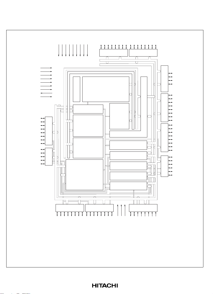
1.2 Block Diagram
5
4
Figure 1.1 shows an internal block diagram of the H8S/2345 Series.
15
14
13
12
11
10
9
8
7
6
/D
/D
/D
/D
1
0
7
6
PE
PE
PD
PD
VCCVCCVCCVSSVSSVSSVSSVSSV
/D
/D
/D
/D
/D
7
SS
PD
PD
/D
6
5
4
3
2
PD
PD
PD
PD
5
4
3
2
1
/D
/D
5
4
PE
PE
0
/D
/D
/D
/D
3
2
1
0
PE
PE
PE
PE
MD
2
MD
1
MD
0
EXTAL
XTAL
STBY
RES
WDTOVF (FWE)
NMI
PF7/ø
PF
/AS
6
PF
/RD
5
PF
/HWR
4
PF
/LWR/IRQ3
3
PF
/WAIT/IRQ2
2
PF
/BACK/IRQ1
1
PF
/BREQ/IRQ0
0
PG4/CS0
PG
/CS1
3
PG
/CS2
2
PG
/CS3/IRQ7
1
PG
/ADTRG/IRQ6
0
Port D
*1
generator
Clock pulse
H8S/2000 CPU
Interrupt controller
DTC
*2
Port
F
ROM
RAM
Port
G
TPU
8-bit timer
D/A converter
A/D converter
WDT
SCI
Port E
Internal data bus
Internal address bus
Bus controller
Port
A
Port
B
Peripheral data bus
Peripheral address bus
Port
C
Port
3
PA
3/A19
PA2/A
18
PA1/A
17
PA0/A
16
PB7/A
15
PB6/A
14
PB5/A
13
PB4/A
12
PB3/A
11
PB2/A
10
PB1/A
9
PB0/A
8
PC7/A
7
PC6/A
6
PC5/A
5
PC4/A
4
PC3/A
3
PC2/A
2
PC1/A
1
PC0/A
0
P3
/SCK1/IRQ
5
P34/SCK0/IRQ
P33/RxD1
P3
/RxD0
2
P3
/TxD1
1
P3
/TxD0
0
22
/TIOCA0/A
P1
20
0
21
/TIOCB0/A
/TIOCC0/TCLKA/A
1
P1
P1
23
/TIOCD0/TCLKB/A
2
3
P1
/TIOCA1
/TIOCB1/TCLKC
4
5
P1
P1
/TIOCA2
/TIOCB2/TCLKD
6
7
P1
P1
/TIOCA3
/TIOCB3
0
1
P2
P2
/TIOCC3/TMRI0
/TIOCD3/TMCI0
/TIOCA4/TMRI1
2
3
4
P2
P2
P2
/TIOCB4/TMCI1
/TIOCA5/TMO0
/TIOCB5/TMO1
5
6
7
P2
P2
P2
ref
V
AVCCAV
Notes: 1. Functions as WDTOVF pin on ZTAT, mask ROM, and ROMless versions.
Functions as FWE pin on F-ZTAT version, not as WDTOVF pin.
2. Not present on ROMless version.
Figure 1.1 Block Diagram
6
Port 4Port 2Port 1
SS
/AN7/DA1
/AN6/DA0
/AN5
/AN4
/AN3
/AN2
/AN1
7
6
5
P4
P4
P4
/AN0
4
3
2
1
P4
0
P4
P4
P4
P4
Page 27

1.3 Pin Description
1.3.1 Pin Arrangement
Figures 1.2 and 1.3 show the pin arrangement of the H8S/2345 Series.
)
*
/BACK/IRQ1
/WAIT/IRQ2
/LWR/IRQ3
/HWR
/RD
/AS
PF0/BREQ/IRQ0
AV
V
P40/AN0
P41/AN1
P42/AN2
P43/AN3
P44/AN4
P45/AN5
P46/AN6/DA0
P47/AN7/DA1
AV
V
P24/TIOCA4/TMRI1
P25/TIOCB4/TMCI1
P26/TIOCA5/TMO0
P27/TIOCB5/TMO1
PG0/ADTRG/IRQ6
PG1/CS3/IRQ7
PG2/CS2
PG3/CS1
PG4/CS0
V
P10/TIOCA0/A
P11/TIOCB0/A
1
2
3
PF
PF
PF
75747372717069686766656463626160595857565554535251
76
77
CC
78
ref
/ø
4
5
6
7
PF
SS
PF
PF
PF
V
EXTAL
XTAL
VCCSTBY
NMI
79
80
81
82
83
84
85
86
87
SS
88
SS
89
90
91
92
93
94
95
96
97
98
CC
99
20
100
21
123456789
22
23
/TIOCA1
/TIOCA2
4
6
P1
P1
/TIOCB1/TCLKC
/TIOCB2/TCLKD
5
7
P1
/TIOCC0/TCLKA/A
/TIOCD0/TCLKB/A
2
3
P1
P1
P1
101112131415161718192021222324
SS
V
/TxD0
/TxD1
/RxD0
/RxD1
0
1
2
3
P3
P3
P3
P3
/SCK0/IRQ4
/SCK1/IRQ5
4
5
P3
P3
RES
0
/D
0
PE
MD2WDTOVF (FWE
1
2
/D
/D
1
2
PE
PE
/TIOCD3/TMCI0
3
P2
3
/D
3
PE
1MD0
MD
SS
V
4
/D
4
PE
19
/A
/TIOCC3/TMRI0
/TIOCB3
/TIOCA3
3
2
1
0
P2
P2
PA
P2
5
6
7
8
/D
/D
/D
/D
5
6
7
0
PE
PE
PE
PD
18
17
/A
/A
2
1
PA
PA
50
PA0/A
V
SS
PB7/A
PB6/A
PB5/A
PB4/A
PB3/A
PB2/A
PB1/A
PB0/A
V
CC
PC7/A
PC6/A
PC5/A
PC4/A
PC3/A
PC2/A
PC1/A
PC0/A
V
SS
PD7/D
PD6/D
PD5/D
PD4/D
PD3/D
16
15
14
13
12
11
10
9
8
7
6
5
4
3
2
1
0
15
14
13
12
11
49
48
47
46
45
44
43
42
41
40
39
38
37
36
35
34
33
32
31
30
29
28
27
26
25
9
10
/D
1
/D
2
PD
PD
Note: * Functions as WDTOVF pin on ZTAT, mask ROM, and ROMless versions.
Functions as FWE pin on F-ZTAT version, not as WDTOVF pin.
Figure 1.2 Pin Arrangement (FP-100B, TFP-100B, TFP-100G*: Top View)
Note: TFP-100G is under development.
7
Page 28

ref
V
/BREQ/IRQ0
AVCCPF
0
/BACK/IRQ1
/WAIT/IRQ2
1
PF
PF
2
/LWR/IRQ3
/HWR
3
PF
PF
)
*
19
18
17
16
/A
/A
/A
PA
/A
3
2
1
0
SS
PA
PA
PA
V
/RD
/AS
/ø
4
5
6
7
SS
PF
PF
PF
V
EXTAL
XTAL
VCCSTBY
NMI
RES
MD2WDTOVF (FWE
/TIOCD3/TMCI0
/TIOCC3/TMRI0
/TIOCB3
2
P2
/TIOCA3
1
P2
P2
P2
1MD0
3
MD
0
P40/AN0
P41/AN1
P4
/AN2
2
P43/AN3
P44/AN4
P4
/AN5
5
P46/AN6/DA0
P47/AN7/DA1
AV
V
P24/TIOCA4/TMRI1
P25/TIOCB4/TMCI1
P2
/TIOCA5/TMO0
6
P27/TIOCB5/TMO1
PG0/ADTRG/IRQ6
PG
/CS3/IRQ7
1
PG2/CS2
PG3/CS1
PG4/CS0
V
8079787776757473727170696867666564636261605958575655545352
81
82
83
84
85
86
87
88
89
SS
90
SS
91
92
93
94
95
96
97
98
99
100
CC
1234567891011121314151617181920212223242526272829
0
1
2
3
4
5
6
7
8
20
21
22
23
/TIOCA0/A
/TIOCB0/A
0
1
P1
P1
/TIOCC0/TCLKA/A
/TIOCD0/TCLKB/A
2
3
P1
P1
V
/TIOCA1
/TIOCA2
4
6
P1
P1
/TIOCB1/TCLKC
/TIOCB2/TCLKD
5
7
P1
P1
SS
/TxD0
/TxD1
0
P3
P3
1
/RxD0
/RxD1
2
3
P3
P3
/SCK0/IRQ4
/SCK1/IRQ5
4
P3
P3
/D
PE
SS
/D
/D
/D
/D
V
1
2
3
4
PE
PE
5
PE
PE
/D
0
PE
5
/D
6
PE
/D
PE
9
/D
/D
7
0
1
PD
PD
/D
PD
51
PB7/A
50
49
48
47
46
45
44
43
42
41
40
39
38
37
36
35
34
33
32
31
30
10
11
12
13
/D
/D
/D
2
3
4
5
PD
PD
PD
PB6/A
PB5/A
PB4/A
PB3/A
PB2/A
PB1/A
PB0/A
V
CC
PC7/A
PC6/A
PC5/A
PC4/A
PC3/A
PC2/A
PC1/A
PC0/A
V
SS
PD7/D
PD6/D
15
14
13
12
11
10
9
8
7
6
5
4
3
2
1
0
15
14
* Functions as WDTOVF pin on ZTAT, mask ROM, and ROMless versions.
Note:
Functions as FWE pin on F-ZTAT version, not as WDTOVF pin.
Figure 1.3 Pin Arrangement (FP-100A: Top View)
8
Page 29

1.3.2 Pin Functions in Each Operating Mode
Table 1.2 shows the pin functions of the H8S/2345 Series in each of the operating modes.
Table 1.2 Pin Functions in Each Operating Mode
Pin No. Pin Name
FP-100B,
TFP-100B,
TFP-100G FP-100A
13P1
Mode
1
*
1
/
2
TIOCC0/
TCLKA
24P1
/
3
TIOCD0/
TCLKB
35P1
46P1
/
4
TIOCA1
/
5
TIOCB1/
TCLKC
57P1
68P1
/
6
TIOCA2
/
7
TIOCB2/
TCLKD
79VSSV
810P3
911P3
/TxD0 P30/TxD0 P30/TxD0 P30/TxD0 P30/TxD0 P30/TxD0 P30/TxD0 NC NC
0
/TxD1 P31/TxD1 P31/TxD1 P31/TxD1 P31/TxD1 P31/TxD1 P31/TxD1 NC NC
1
Mode
*
2
P1
TIOCC0/
TCLKA
P1
TIOCD0/
TCLKB
P14/
TIOCA1
P1
TIOCB1/
TCLKC
P16/
TIOCA2
P1
TIOCB2/
TCLKD
SS
1, *2
2
3
5
7
Mode
*
3
/
P1
TIOCC0/
TCLKA
/
P1
TIOCD0/
TCLKB
P14/
TIOCA1
/
P1
TIOCB1/
TCLKC
P16/
TIOCA2
/
P1
TIOCB2/
TCLKD
V
SS
Mode4Mode5Mode
1, *2
/
2
/
P1
2
TIOCC0/
TCLKA/
A
22
/
3
/
P1
3
TIOCD0/
TCLKB/
A
23
P14/
TIOCA1
/
5
/
P1
5
TIOCB1/
TCLKC
P16/
TIOCA2
/
7
/
P1
7
TIOCB2/
TCLKD
V
SS
P12/
TIOCC0/
TCLKA/
A
22
P13/
TIOCD0/
TCLKB/
A
23
P14/
TIOCA1
/
P1
5
TIOCB1/
TCLKC
P16/
TIOCA2
/
P1
7
TIOCB2/
TCLKD
V
SS
2
*
6
P12/
TIOCC0/
TCLKA/
A
22
P13/
TIOCD0/
TCLKB/
A
23
P14/
TIOCA1
/
P1
5
TIOCB1/
TCLKC
P16/
TIOCA2
/
P1
7
TIOCB2/
TCLKD
V
SS
Mode
2
*
7
P12/
TIOCC0/
TCLKA
P13/
TIOCD0/
TCLKB
P14/
TIOCA1
/
P1
5
TIOCB1/
TCLKC
P16/
TIOCA2
/
P1
7
TIOCB2/
TCLKD
V
SS
10 12 P32/RxD0 P32/RxD0 P32/RxD0 P32/RxD0 P32/RxD0 P32/RxD0 P32/RxD0 NC NC
11 13 P33/RxD1 P33/RxD1 P33/RxD1 P33/RxD1 P33/RxD1 P33/RxD1 P33/RxD1 NC NC
12 14 P34/
SCK0/
IRQ4
13 15 P35/
SCK1/
IRQ5
14 16 PE0/D0PE0/D0PE
15 17 PE1/D1PE1/D1PE
16 18 PE2/D2PE2/D2PE
17 19 PE3/D3PE3/D3PE
18 20 V
SS
19 21 PE4/D4PE4/D4PE
/
P3
4
SCK0/
IRQ4
/
P3
5
SCK1/
IRQ5
V
SS
/
P3
4
SCK0/
IRQ4
/
P3
5
SCK1/
IRQ5
0
1
2
3
V
SS
4
/
P3
4
SCK0/
IRQ4
/
P3
5
SCK1/
IRQ5
/
P3
4
SCK0/
IRQ4
/
P3
5
SCK1/
IRQ5
/
P3
4
SCK0/
IRQ4
/
P3
5
SCK1/
IRQ5
P3
SCK0/
IRQ4
P3
SCK1/
IRQ5
PE0/D0PE0/D0PE0/D0PE
PE1/D1PE1/D1PE1/D1PE
PE2/D2PE2/D2PE2/D2PE
PE3/D3PE3/D3PE3/D3PE
V
SS
V
SS
V
SS
V
PE4/D4PE4/D4PE4/D4PE
/
4
/
5
0
1
2
3
SS
4
Flash
Memory
PROM
Writer
3
*
Mode
Mode
NC NC
NC NC
NC NC
NC NC
NC NC
NC NC
V
V
SS
NC NC
NC NC
NC NC
NC NC
NC NC
NC NC
V
V
SS
NC NC
4
*
SS
SS
9
Page 30

Table 1.2 Pin Functions in Each Operating Mode (cont)
Pin No. Pin Name
FP-100B,
TFP-100B,
TFP-100G FP-100A
Mode
*
1
20 22 PE5/D5PE5/D5PE
21 23 PE6/D6PE6/D6PE
22 24 PE7/D7PE7/D7PE
23 25 D
24 26 D
25 27 D
26 28 D
27 29 D
28 30 D
29 31 D
30 32 D
31 33 V
32 34 A
33 35 A
34 36 A
35 37 A
36 38 A
37 39 A
38 40 A
39 41 A
40 42 V
41 43 A
42 44 A
43 45 A
44 46 A
45 47 A
46 48 A
47 49 A
48 50 A
49 51 V
8
9
10
11
12
13
14
15
SS
0
1
2
3
4
5
6
7
CC
8
9
10
11
12
13
14
15
SS
50 52 PA
51 53 PA
1
0
1
Mode
*
2
D
8
D
9
D
10
D
11
D
12
D
13
D
14
D
15
V
SS
1, *2
Mode
3
PD
PD
PD
PD
PD
PD
PD
PD
V
PC0/A0PC
PC1/A1PC
PC2/A2PC
PC3/A3PC
PC4/A4PC
PC5/A5PC
PC6/A6PC
PC7/A7PC
V
CC
V
PB0/A8PB
PB1/A9PB
PB2/A10PB
PB3/A11PB
PB4/A12PB
PB5/A13PB
PB6/A14PB
PB7/A15PB
V
PA
PA
SS
V
PA
0
PA
1
Mode4Mode5Mode
1, *2
*
PE5/D5PE5/D5PE5/D5PE
5
PE6/D6PE6/D6PE6/D6PE
6
PE7/D7PE7/D7PE7/D7PE
7
D
0
1
2
3
4
5
6
7
SS
0
1
2
3
4
5
6
7
CC
0
1
2
3
4
5
6
7
SS
0
1
8
D
9
D
10
D
11
D
12
D
13
D
14
D
15
V
SS
A
0
A
1
A
2
A
3
A
4
A
5
A
6
A
7
V
CC
A
8
A
9
A
10
A
11
A
12
A
13
A
14
A
15
V
SS
A
16
A
17
D
8
D
9
D
10
D
11
D
12
D
13
D
14
D
15
V
SS
A
0
A
1
A
2
A
3
A
4
A
5
A
6
A
7
V
CC
A
8
A
9
A
10
A
11
A
12
A
13
A
14
A
15
V
SS
A
16
A
17
2
*
6
D
8
D
9
D
10
D
11
D
12
D
13
D
14
D
15
V
SS
Mode
7
PD
PD
PD
PD
PD
PD
PD
PD
V
PC0/A0PC
PC1/A1PC
PC2/A2PC
PC3/A3PC
PC4/A4PC
PC5/A5PC
PC6/A6PC
PC7/A7PC
V
CC
V
PB0/A8PB
PB1/A9PB
PB2/A10PB
PB3/A11PB
PB4/A12PB
PB5/A13PB
PB6/A14PB
PB7/A15PB
V
SS
V
PA0/A16PA
PA1/A17PA
Flash
Memory
PROM
2
*
5
6
7
0
1
2
3
4
5
6
7
SS
0
1
2
3
4
5
6
7
CC
0
1
2
3
4
5
6
7
SS
0
1
Writer
3
*
Mode
Mode
NC NC
NC NC
NC NC
EO0FO
EO1FO
EO2FO
EO3FO
EO4FO
EO5FO
EO6FO
EO7FO
V
V
SS
EA
FA
0
EA
FA
1
EA
FA
2
EA
FA
3
EA
FA
4
EA
FA
5
EA
FA
6
EA
FA
7
V
V
CC
EA
FA
8
OE FA
EA
FA
10
EA
FA
11
EA
FA
12
EA
FA
13
EA
FA
14
EA
FA
15
V
V
SS
EA
FA
16
V
NC
CC
4
*
0
1
2
3
4
5
6
7
SS
0
1
2
3
4
5
6
7
CC
8
9
10
11
12
13
14
15
SS
16
10
Page 31

Table 1.2 Pin Functions in Each Operating Mode (cont)
Pin No. Pin Name
FP-100B,
TFP-100B,
TFP-100G FP-100A
Mode
*
1
52 54 PA
53 55 PA
54 56 P20/
TIOCA3
55 57 P21/
TIOCB3
56 58 P22/
TIOCC3/
TMRI0
57 59 MD
58 60 MD
59 61 P23/
TIOCD3/
TMCI0
Mode
1
2
3
2
PA
PA
*
P20/
TIOCA3
P21/
TIOCB3
P2
TIOCC3/
TMRI0
MD
0
MD
1
P2
TIOCD3/
TMCI0
60 62 WDTOVF WDTOVF WDTOVF WDTOVF
61 63 MD
MD
2
1, *2
2
3
2
3
Mode
*
3
PA
PA
P20/
TIOCA3
P21/
TIOCB3
/
P2
TIOCC3/
TMRI0
MD
0
MD
1
/
P2
TIOCD3/
TMCI0
MD
2
Mode4Mode5Mode
1, *2
A
2
3
18
A
19
P20/
TIOCA3
P21/
TIOCB3
/
2
/
P2
2
TIOCC3/
TMRI0
MD
0
1
/
3
0
MD
1
/
P2
3
TIOCD3/
TMCI0
5
*
)
(FWE
MD
2
2
A
18
A
19
P20/
TIOCA3
P21/
TIOCB3
/
P2
2
TIOCC3/
TMRI0
MD
0
MD
1
/
P2
3
TIOCD3/
TMCI0
WDTOVF
5
*
(FWE
MD
2
2
*
6
PA2/A18PA
PA3/A19PA
P20/
TIOCA3
P21/
TIOCB3
P2
2
TIOCC3/
TMRI0
MD
MD
P2
3
TIOCD3/
TMCI0
WDTOVF
)
(FWE
MD
Mode
2
*
7
2
3
P20/
TIOCA3
P21/
TIOCB3
/
/
P2
2
TIOCC3/
TMRI0
MD
0
1
/
0
MD
1
/
P2
3
TIOCD3/
TMCI0
WDTOVF
5
*
)
2
(FWE
MD
5
*
)
2
62 64 RES RES RES RES RES RES RES V
63 65 NMI NMI NMI NMI NMI NMI NMI EA
64 66 STBY STBY STBY STBY STBY STBY STBY V
65 67 V
CC
V
CC
V
CC
V
CC
V
CC
V
CC
V
CC
66 68 XTAL XTAL XTAL XTAL XTAL XTAL XTAL NC XTAL
67 69 EXTAL EXTAL EXTAL EXTAL EXTAL EXTAL EXTAL NC EXTAL
68 70 V
SS
V
SS
V
SS
V
SS
V
SS
V
SS
V
SS
69 71 PF7/ø PF7/ø PF7/ø PF7/ø PF7/ø PF7/ø PF7/ø NC NC
70 72 AS AS PF
71 73 RD RD PF
72 74 HWR HWR PF
AS AS AS PF
6
RD RD RD PF
5
HWR HWR HWR PF
4
6
5
4
73 75 LWR LWR PF3/IRQ3 LWR LWR LWR PF3/IRQ3 NC NC
74 76 PF2/
WAIT/
IRQ2
75 77 PF1/
BACK/
IRQ1
/
PF
2
WAIT/
IRQ2
/
PF
1
BACK/
IRQ1
/IRQ2 PF2/
PF
2
/IRQ1 PF1/
PF
1
WAIT/
IRQ2
BACK/
IRQ1
/
PF
2
WAIT/
IRQ2
/
PF
1
BACK/
IRQ1
/
PF
2
WAIT/
IRQ2
/
PF
1
BACK/
IRQ1
/IRQ2 CE V
PF
2
/IRQ1 PGM V
PF
1
Flash
Memory
PROM
Writer
3
*
Mode
Mode
V
NC
CC
NC NC
NC OE
NC CE
NC WE
V
V
SS
SS
V
V
SS
SS
NC V
CC
NC FWE
V
V
SS
SS
RES
PP
V
9
CC
V
SS
CC
V
V
CC
CC
V
V
SS
SS
NC NC
NC NC
NC NC
CC
SS
4
*
11
Page 32

Table 1.2 Pin Functions in Each Operating Mode (cont)
Pin No. Pin Name
FP-100B,
TFP-100B,
TFP-100G FP-100A
Mode
*
1
76 78 PF0/
BREQ/
IRQ0
77 79 AV
78 80 V
Mode
1
*
2
PF
BREQ/
IRQ0
AV
CC
ref
V
ref
1, *2
0
CC
Mode
*
3
/
PF
AV
V
ref
Mode4Mode5Mode
1, *2
/IRQ0 PF0/
0
BREQ/
IRQ0
AV
CC
CC
V
ref
/
PF
0
BREQ/
IRQ0
AV
CC
V
ref
2
*
6
/
PF
0
BREQ/
IRQ0
AV
CC
V
ref
Mode
2
*
7
/IRQ0 NC V
PF
0
AV
CC
V
ref
79 81 P40/AN0 P40/AN0 P40/AN0 P40/AN0 P40/AN0 P40/AN0 P40/AN0 NC NC
80 82 P41/AN1 P41/AN1 P41/AN1 P41/AN1 P41/AN1 P41/AN1 P41/AN1 NC NC
81 83 P42/AN2 P42/AN2 P42/AN2 P42/AN2 P42/AN2 P42/AN2 P42/AN2 NC NC
82 84 P43/AN3 P43/AN3 P43/AN3 P43/AN3 P43/AN3 P43/AN3 P43/AN3 NC NC
83 85 P44/AN4 P44/AN4 P44/AN4 P44/AN4 P44/AN4 P44/AN4 P44/AN4 NC NC
84 86 P45/AN5 P45/AN5 P45/AN5 P45/AN5 P45/AN5 P45/AN5 P45/AN5 NC NC
85 87 P46/AN6/
DA0
86 88 P47/AN7/
DA1
87 89 AV
88 90 V
SS
89 91 P24/
TIOCA4/
TMRI1
90 92 P25/
TIOCB4/
TMCI1
91 93 P26/
TIOCA5/
TMO0
92 94 P27/
TIOCB5/
TMO1
93 95 PG0/
IRQ6/
ADTRG
94 96 PG1/IRQ7 PG1/IRQ7 PG1/IRQ7 PG1/CS3/
95 97 PG
96 98 PG
97 99 PG4/CS0 PG4/CS0 PG
P46/AN6/
DA0
P47/AN7/
DA1
AV
SS
V
SS
P2
TIOCA4/
TMRI1
P2
TIOCB4/
TMCI1
P2
TIOCA5/
TMO0
P2
TIOCB5/
TMO1
PG
IRQ6/
ADTRG
PG
2
PG
3
P46/AN6/
DA0
P47/AN7/
DA1
AV
SS
V
SS
/
P2
4
TIOCA4/
TMRI1
/
P2
5
TIOCB4/
TMCI1
/
P2
6
TIOCA5/
TMO0
/
P2
7
TIOCB5/
TMO1
/
PG
0
IRQ6/
ADTRG
PG
2
PG
3
P46/AN6/
DA0
P47/AN7/
DA1
AV
SS
V
SS
/
P2
4
TIOCA4/
TMRI1
/
P2
5
TIOCB4/
TMCI1
/
P2
6
TIOCA5/
TMO0
/
P2
7
TIOCB5/
TMO1
/
PG
0
IRQ6/
ADTRG
P46/AN6/
DA0
P47/AN7/
DA1
AV
SS
/
4
SS
V
SS
/
P2
4
TIOCA4/
TMRI1
/
5
/
P2
5
TIOCB4/
TMCI1
/
6
/
P2
6
TIOCA5/
TMO0
/
7
/
P2
7
TIOCB5/
TMO1
/
0
PG
0
IRQ6/
/
ADTRG
PG1/CS3/
IRQ7
PG2/CS2 PG2/CS2 PG2/CS2 PG
2
PG3/CS1 PG3/CS1 PG3/CS1 PG
3
PG4/CS0 PG4/CS0 PG4/CS0 PG
4
IRQ7
P46/AN6/
DA0
P47/AN7/
DA1
AV
SS
V
SS
/
P2
4
TIOCA4/
TMRI1
/
P2
5
TIOCB4/
TMCI1
/
P2
6
TIOCA5/
TMO0
/
P2
7
TIOCB5/
TMO1
/
PG
0
IRQ6/
ADTRG
PG1/CS3/
IRQ7
P46/AN6/
DA0
P47/AN7/
DA1
AV
SS
V
SS
/
P2
4
TIOCA4/
TMRI1
/
P2
5
TIOCB4/
TMCI1
/
P2
6
TIOCA5/
TMO0
/
P2
7
TIOCB5/
TMO1
/
PG
0
IRQ6/
ADTRG
PG1/IRQ7 NC NC
2
3
4
Flash
Memory
PROM
Writer
3
*
Mode
Mode
V
V
CC
V
V
CC
NC NC
NC NC
V
V
SS
V
V
SS
NC NC
NC V
NC NC
NC NC
NC NC
NC NC
NC NC
NC NC
4
*
SS
CC
CC
SS
SS
CC
12
Page 33

Table 1.2 Pin Functions in Each Operating Mode (cont)
Pin No. Pin Name
FP-100B,
TFP-100B,
TFP-100G FP-100A
98 100 V
Mode
*
1
CC
99 1 P10/
TIOCA0
100 2 P11/
TIOCB0
Notes: 1. Modes 1 to 3 are not available on the F-ZTAT version.
2. Modes 2, 3, 6, and 7 are not available on the ROMless version.
3. ZTAT version only.
4. F-ZTAT version only.
5. The FWE pin is only used on the F-ZTAT version. It cannot be used as a WDTOVF pin
on the F-ZTAT version.
Mode
1
*
2
V
CC
P10/
TIOCA0
P11/
TIOCB0
1, *2
Mode
1, *2
*
3
V
CC
P10/
TIOCA0
P11/
TIOCB0
Mode4Mode5Mode
V
CC
P10/
TIOCA0/
A
20
P11/
TIOCB0/
A
21
V
CC
P10/
TIOCA0/
A
20
P11/
TIOCB0/
A
21
2
*
6
V
CC
P10/
TIOCA0/
A
20
P11/
TIOCB0/
A
21
Mode
2
*
7
V
CC
P10/
TIOCA0
P11/
TIOCB0
Flash
Memory
PROM
Writer
3
*
Mode
Mode
V
V
CC
NC NC
NC NC
4
*
CC
13
Page 34

1.3.3 Pin Functions
Table 1.3 outlines the pin functions of the H8S/2345 Series.
Table 1.3 Pin Functions
Pin No.
FP-100B,
TFP-100B,
Type Symbol
Power V
CC
V
SS
Clock XTAL 66 68 Input Connects to a crystal oscillator.
EXTAL 67 69 Input Connects to a crystal oscillator.
ø 69 71 Output System clock: Supplies the system
TFP-100G FP-100A I/O Name and Function
40, 65,9842, 67,
100
Input Power supply: For connection to the
power supply. All V
connected to the system power
supply.
7, 18,
31, 49,
68, 88
9, 20,
33, 51,
70, 90
Input Ground: For connection to ground
(0 V). All V
pins should be
SS
connected to the system power
supply (0 V).
See section 18, Clock Pulse
Generator, for typical connection
diagrams for a crystal oscillator and
external clock input.
The EXTAL pin can also input an
external clock.
See section 18, Clock Pulse
Generator, for typical connection
diagrams for a crystal oscillator and
external clock input.
clock to an external device.
pins should be
CC
14
Page 35

Table 1.3 Pin Functions (cont)
FP-100B,
TFP-100B,
Type Symbol
Operating mode
control
MD2 to
MD
0
TFP-100G FP-100A I/O Name and Function
61, 58,5763, 60,59Input Mode pins: These pins set the
Pin No.
operating mode.
The relation between the settings of
pins MD
to MD0 and the operating
2
mode is shown below. These pins
should not be changed while the
H8S/2345 Series is operating.
• F-ZTAT Version
Operating
FWE MD2MD1MD
0
Mode
0 000—
1—
10—
1—
1 0 0 Mode 4
1 Mode 5
1 0 Mode 6
1 Mode 7
1 000—
1—
1 0 Mode 10
1 Mode 11
100—
1—
1 0 Mode 14
1 Mode 15
15
Page 36

Table 1.3 Pin Functions (cont)
Pin No.
FP-100B,
TFP-100B,
Type Symbol
Operating mode
control
MD2 to
MD
0
System control RES 62 64 Input Reset input: When this pin is driven
STBY 64 66 Input Standby: When this pin is driven low,
BREQ 76 78 Input Bus request: Used by an external
BACK 75 77 Output Bus request acknowledge: Indicates
*
FWE
TFP-100G FP-100A I/O Name and Function
61, 58,5763, 60,59Input
• ZTAT, mask ROM, and ROMless
versions
MD2MD1MD
000—
1 Mode 1
1 0 Mode 2*
1 Mode 3*
1 0 0 Mode 4
1 Mode 5
1 0 Mode 6*
1 Mode 7*
Note: * Not used on ROMless
version.
low, the chip is reset. The type of
reset can be selected according to
the NMI input level. At power-on, the
NMI pin input level should be set
high.
a transition is made to hardware
standby mode.
bus master to issue a bus request to
the H8S/2345 Series.
that the bus has been released to an
external bus master.
1
60 62 Input Flash write enable: Enables or
disables writing to flash memory.
Operating
Mode
0
16
Page 37

Table 1.3 Pin Functions (cont)
Pin No.
FP-100B,
TFP-100B,
Type Symbol
Interrupts NMI 63 65 Input Nonmaskable interrupt: Requests a
IRQ7 to
IRQ0
Address bus A23 to
A
0
Data bus D15 to
D
0
Bus control CS3 to
CS0
AS 70 72 Output Address strobe: When this pin is low,
RD 71 73 Output Read: When this pin is low, it
HWR 72 74 Output High write: A strobe signal that writes
LWR 73 75 Output Low write: A strobe signal that writes
WAIT 74 76 Input Wait: Requests insertion of a wait
TFP-100G FP-100A I/O Name and Function
nonmaskable interrupt. When this pin
is not used, it should be fixed high.
94, 93,
13, 12,
73 to 76
2, 1,
100, 99,
53 to 50,
48 to 41,
96, 95,
15, 14,
75 to 78
4 to 1,
55 to 52,
50 to 43,
41 to 34
Input Interrupt request 7 to 0: These pins
request a maskable interrupt.
Output Address bus: These pins output an
address.
39 to 32
30 to 19,
17 to 14
32 to 21,
19 to 16
I/O Data bus: These pins constitute a
bidirectional data bus.
94 to 97 96 to 99 Output Chip select: Signals for selecting
areas 3 to 0.
it indicates that address output on the
address bus is enabled.
indicates that the external address
space can be read.
to external space and indicates that
the upper half (D
to D8) of the data
15
bus is enabled.
to external space and indicates that
the lower half (D
to D0) of the data
7
bus is enabled.
state in the bus cycle when
accessing external 3-state address
space.
17
Page 38

Table 1.3 Pin Functions (cont)
FP-100B,
TFP-100B,
Type Symbol
16-bit timerpulse unit
TCLKD to
TCLKA
(TPU)
TIOCA0,
TIOCB0,
TIOCC0,
TIOCD0
TIOCA1,
TIOCB1
TIOCA2,
TIOCB2
TIOCA3,
TIOCB3,
TIOCC3,
TIOCD3
TIOCA4,
TIOCB4
TIOCA5,
TIOCB5
8-bit timer TMO0,
TMO1
TMCI0,
TMCI1
TMRI0,
TMRI1
Watchdog
WDTOVF
timer (WDT)
TFP-100G FP-100A I/O Name and Function
6, 4, 2, 1 8, 6, 4, 3 Input Clock input D to A: These pins input
99, 100,
1, 2
3, 4 5, 6 I/O Input capture/ output compare match
5, 6 7, 8 I/O Input capture/ output compare match
54 to 56,5956 to 58,61I/O Input capture/ output compare match
89, 90 91, 92 I/O Input capture/ output compare match
91, 92 93, 94 I/O Input capture/ output compare match
91, 92 93, 94 Output Compare match output: The compare
59, 90 61, 92 Input Counter external clock input: Input
56, 89 58, 91 Input Counter external reset input: The
2
*
60 62 Output Watchdog timer overflows: The
Pin No.
an external clock.
1 to 4 I/O Input capture/ output compare match
A0 to D0: The TGR0A to TGR0D
input capture input or output compare
output, or PWM output pins.
A1 and B1: The TGR1A and TGR1B
input capture input or output compare
output, or PWM output pins.
A2 and B2: The TGR2A and TGR2B
input capture input or output compare
output, or PWM output pins.
A3 to D3: The TGR3A to TGR3D
input capture input or output compare
output, or PWM output pins.
A4 and B4: The TGR4A and TGR4B
input capture input or output compare
output, or PWM output pins.
A5 and B5: The TGR5A and TGR5B
input capture input or output compare
output, or PWM output pins.
match output pins.
pins for the external clock input to the
counter.
counter reset input pins.
counter overflows signal output pin in
watchdog timer mode.
18
Page 39

Table 1.3 Pin Functions (cont)
Pin No.
FP-100B,
TFP-100B,
Type Symbol
Serial
communication
interface (SCI)
Smart Card
TxD1,
TxD0
RxD1,
RxD0
interface
SCK1
SCK0
A/D converter AN7 to
AN0
ADTRG 93 95 Input A/D conversion external trigger input:
D/A converter DA1, DA0 86, 85 88, 87 Output Analog output: D/A converter analog
A/D converter
AV
CC
and D/A
converters
AV
SS
V
ref
I/O ports P17 to
P1
0
P27 to
P2
0
TFP-100G FP-100A I/O Name and Function
9, 8 11, 10 Output Transmit data (channel 0, 1):
Data output pins.
11, 10 13, 12 Input Receive data (channel 0, 1):
Data input pins.
13, 12 15, 14 I/O Serial clock (channel 0, 1):
Clock I/O pins.
86 to 79 88 to 81 Input Analog 7 to 0: Analog input pins.
Pin for input of an external trigger to
start A/D conversion.
output pins.
77 79 Input This is the power supply pin for the
A/D converter and D/A converter.
When the A/D converter and D/A
converter are not used, this pin
should be connected to the system
power supply (+5 V).
87 89 Input This is the ground pin for the A/D
converter and D/A converter.
This pin should be connected to the
system power supply (0 V).
78 80 Input This is the reference voltage input pin
for the A/D converter and D/A
converter.
When the A/D converter and D/A
converter are not used, this pin
should be connected to the system
power supply (+5 V).
6 to 1,
100, 99
8 to 1 I/O Port 1: An 8-bit I/O port. Input or
output can be designated for each bit
by means of the port 1 data direction
register (P1DDR).
92 to 89,
59,
56 to 54
94 to 91,
61,
58 to 56
I/O Port 2: An 8-bit I/O port. Input or
output can be designated for each bit
by means of the port 2 data direction
register (P2DDR).
19
Page 40

Table 1.3 Pin Functions (cont)
FP-100B,
TFP-100B,
Type Symbol
I/O ports P35 to
P3
0
P47 to
P4
0
PA3 to
PA
0
PB7 to
PB
0
PC7 to
PC
0
PD7 to
PD
0
PE7 to
PE
0
PF7 to
PF
0
PG4 to
PG
0
Notes: 1. F-ZTAT version only.
2. Applies to ZTAT, mask ROM, and ROMless versions only.
TFP-100G FP-100A I/O Name and Function
13 to 8 15 to 10 I/O Port 3: A 6-bit I/O port. Input or
86 to 79 88 to 81 Input Port 4: An 8-bit input port.
53 to 50 55 to 52 I/O Port A: An 4-bit I/O port. Input or
48 to 41 50 to 43 I/O Port B: An 8-bit I/O port. Input or
39 to 32 41 to 34 I/O Port C: An 8-bit I/O port. Input or
30 to 23 32 to 25 I/O Port D: An 8-bit I/O port. Input or
22 to 19,
17 to 14
69 to 76 71 to 78 I/O Port F: An 8-bit I/O port. Input or
97 to 93 99 to 95 I/O Port G: A 5-bit I/O port. Input or
Pin No.
24 to 21,
19 to 16
output can be designated for each bit
by means of the port 3 data direction
register (P3DDR).
output can be designated for each bit
by means of the port A data direction
register (PADDR).
output can be designated for each bit
by means of the port B data direction
register (PBDDR).
output can be designated for each bit
by means of the port C data direction
register (PCDDR).
output can be designated for each bit
by means of the port D data direction
register (PDDDR).
I/O Port E: An 8-bit I/O port. Input or
output can be designated for each bit
by means of the port E data direction
register (PEDDR).
output can be designated for each bit
by means of the port F data direction
register (PFDDR).
output can be designated for each bit
by means of the port G data direction
register (PGDDR).
20
Page 41

Section 2 CPU
2.1 Overview
The H8S/2000 CPU is a high-speed central processing unit with an internal 32-bit architecture that
is upward-compatible with the H8/300 and H8/300H CPUs. The H8S/2000 CPU has sixteen 16-bit
general registers, can address a 16-Mbyte (architecturally 4-Gbyte) linear address space, and is
ideal for realtime control.
2.1.1 Features
The H8S/2000 CPU has the following features.
• Upward-compatible with H8/300 and H8/300H CPUs
Can execute H8/300 and H8/300H object programs
• General-register architecture
Sixteen 16-bit general registers (also usable as sixteen 8-bit registers or eight 32-bit
registers)
• Sixty-five basic instructions
8/16/32-bit arithmetic and logic instructions
Multiply and divide instructions
Powerful bit-manipulation instructions
• Eight addressing modes
Register direct [Rn]
Register indirect [@ERn]
Register indirect with displacement [@(d:16,ERn) or @(d:32,ERn)]
Register indirect with post-increment or pre-decrement [@ERn+ or @–ERn]
Absolute address [@aa:8, @aa:16, @aa:24, or @aa:32]
Immediate [#xx:8, #xx:16, or #xx:32]
Program-counter relative [@(d:8,PC) or @(d:16,PC)]
Memory indirect [@@aa:8]
• 16-Mbyte address space
Program: 16 Mbytes
Data: 16 Mbytes (4 Gbytes architecturally)
21
Page 42

• High-speed operation
All frequently-used instructions execute in one or two states
Maximum clock rate : 20 MHz
8/16/32-bit register-register add/subtract : 50 ns
8 × 8-bit register-register multiply : 600 ns
16 ÷ 8-bit register-register divide : 600 ns
16 × 16-bit register-register multiply : 1000 ns
32 ÷ 16-bit register-register divide : 1000 ns
• Two CPU operating modes
Normal mode (Supported on ZTAT, mask ROM, and ROMless versions only)
Advanced mode
• Power-down state
Transition to power-down state by SLEEP instruction
CPU clock speed selection
2.1.2 Differences between H8S/2600 CPU and H8S/2000 CPU
The differences between the H8S/2600 CPU and the H8S/2000 CPU are as shown below.
• Register configuration
The MAC register is supported only by the H8S/2600 CPU.
• Basic instructions
The four instructions MAC, CLRMAC, LDMAC, and STMAC are supported only by the
H8S/2600 CPU.
• Number of execution states
The number of execution states of the MULXU and MULXS instructions.
Internal Operation
Instruction Mnemonic H8S/2600 H8S/2000
MULXU MULXU.B Rs, Rd 3 12
MULXU.W Rs, ERd 4 20
MULXS MULXS.B Rs, Rd 4 13
MULXS.W Rs, ERd 5 21
There are also differences in the address space, CCR and EXR register functions, power-down
state, etc., depending on the product.
22
Page 43

2.1.3 Differences from H8/300 CPU
In comparison to the H8/300 CPU, the H8S/2000 CPU has the following enhancements.
• More general registers and control registers
Eight 16-bit expanded registers, and one 8-bit control register, have been added.
• Expanded address space
Normal mode supports the same 64-kbyte address space as the H8/300 CPU. (ZTAT, mask
ROM, and ROMless versions only)
Advanced mode supports a maximum 16-Mbyte address space.
• Enhanced addressing
The addressing modes have been enhanced to make effective use of the 16-Mbyte address
space.
• Enhanced instructions
Addressing modes of bit-manipulation instructions have been enhanced.
Signed multiply and divide instructions have been added.
Two-bit shift instructions have been added.
Instructions for saving and restoring multiple registers have been added.
A test and set instruction has been added.
• Higher speed
Basic instructions execute twice as fast.
2.1.4 Differences from H8/300H CPU
In comparison to the H8/300H CPU, the H8S/2000 CPU has the following enhancements.
• Additional control register
One 8-bit control register has been added.
• Enhanced instructions
Addressing modes of bit-manipulation instructions have been enhanced.
Two-bit shift instructions have been added.
Instructions for saving and restoring multiple registers have been added.
A test and set instruction has been added.
• Higher speed
Basic instructions execute twice as fast.
23
Page 44
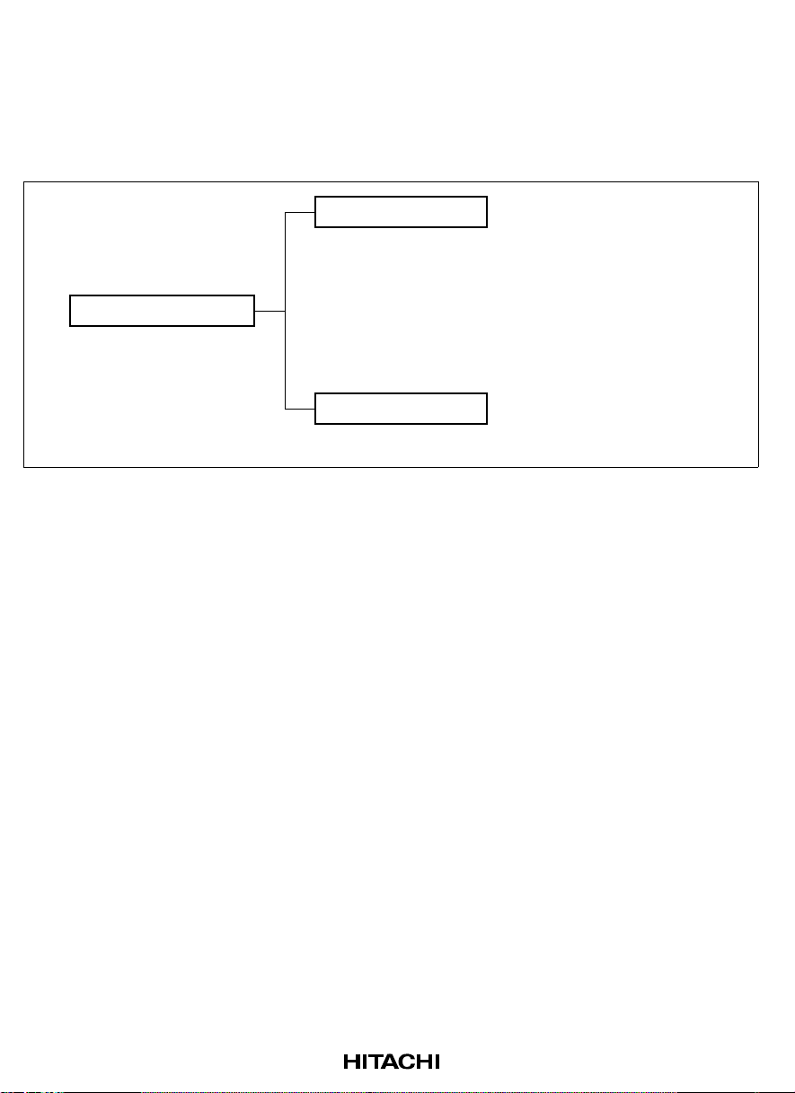
2.2 CPU Operating Modes
The H8S/2000 CPU has two operating modes: normal and advanced. Normal mode supports a
maximum 64-kbyte address space. Advanced mode supports a maximum 16-Mbyte total address
space (architecturally a maximum 16-Mbyte program area and a maximum of 4 Gbytes for
program and data areas combined). The mode is selected by the mode pins of the microcontroller.
Normal mode
(Supported on ZTAT,
mask ROM, and ROMless
versions only)
CPU operating modes
Advanced mode
Maximum 64 kbytes, program
and data areas combined
Maximum 16-Mbytes for
program and data areas
combined
Figure 2.1 CPU Operating Modes
(1) Normal Mode (ZTAT, Mask ROM, and ROMless Versions Only)
The exception vector table and stack have the same structure as in the H8/300 CPU.
Address Space: A maximum address space of 64 kbytes can be accessed.
Extended Registers (En): The extended registers (E0 to E7) can be used as 16-bit registers, or as
the upper 16-bit segments of 32-bit registers. When En is used as a 16-bit register it can contain
any value, even when the corresponding general register (Rn) is used as an address register. If the
general register is referenced in the register indirect addressing mode with pre-decrement (@–Rn)
or post-increment (@Rn+) and a carry or borrow occurs, however, the value in the corresponding
extended register (En) will be affected.
Instruction Set: All instructions and addressing modes can be used. Only the lower 16 bits of
effective addresses (EA) are valid.
24
Page 45

Exception Vector Table and Memory Indirect Branch Addresses: In normal mode the top area
starting at H'0000 is allocated to the exception vector table. One branch address is stored per 16
bits. The configuration of the exception vector table in normal mode is shown in figure 2.2. For
details of the exception vector table, see section 4, Exception Handling.
H'0000
H'0001
H'0002
H'0003
H'0004
H'0005
H'0006
H'0007
H'0008
H'0009
H'000A
H'000B
Power-on reset exception vector
Manual reset exception vector
(Reserved for system use)
Exception vector 1
Exception vector 2
Exception
vector table
Figure 2.2 Exception Vector Table (Normal Mode)
The memory indirect addressing mode (@@aa:8) employed in the JMP and JSR instructions uses
an 8-bit absolute address included in the instruction code to specify a memory operand that
contains a branch address. In normal mode the operand is a 16-bit word operand, providing a 16bit branch address. Branch addresses can be stored in the top area from H'0000 to H'00FF. Note
that this area is also used for the exception vector table.
25
Page 46

Stack Structure: When the program counter (PC) is pushed onto the stack in a subroutine call,
and the PC, condition-code register (CCR), and extended control register (EXR) are pushed onto
the stack in exception handling, they are stored as shown in figure 2.3. When EXR is invalid, it is
not pushed onto the stack. For details, see section 4, Exception Handling.
SP
Notes: 1.
PC
(16 bits)
(a) Subroutine Branch (b) Exception Handling
When EXR is not used it is not stored on the stack.
2.
SP when EXR is not used.
3.
Ignored when returning.
SP
*2
(SP )
Reserved
*1
EXR
CCR
*3
CCR
PC
(16 bits)
*1,*3
Figure 2.3 Stack Structure in Normal Mode
(2) Advanced Mode
Address Space: Linear access is provided to a 16-Mbyte maximum address space (architecturally
a maximum 16-Mbyte program area and a maximum 4-Gbyte data area, with a maximum of 4
Gbytes for program and data areas combined).
Extended Registers (En): The extended registers (E0 to E7) can be used as 16-bit registers, or as
the upper 16-bit segments of 32-bit registers or address registers.
Instruction Set: All instructions and addressing modes can be used.
26
Page 47

Exception Vector Table and Memory Indirect Branch Addresses: In advanced mode the top
area starting at H'00000000 is allocated to the exception vector table in units of 32 bits. In each 32
bits, the upper 8 bits are ignored and a branch address is stored in the lower 24 bits (figure 2.4).
For details of the exception vector table, see section 4, Exception Handling.
H'00000000
H'00000003
H'00000004
H'00000007
H'00000008
H'0000000B
H'0000000C
H'00000010
Reserved
Power-on reset exception vector
Reserved
Manual reset exception vector
Exception vector table
(Reserved for system use)
Reserved
Exception vector 1
Figure 2.4 Exception Vector Table (Advanced Mode)
The memory indirect addressing mode (@@aa:8) employed in the JMP and JSR instructions uses
an 8-bit absolute address included in the instruction code to specify a memory operand that
contains a branch address. In advanced mode the operand is a 32-bit longword operand, providing
a 32-bit branch address. The upper 8 bits of these 32 bits are a reserved area that is regarded as
H'00. Branch addresses can be stored in the area from H'00000000 to H'000000FF. Note that the
first part of this range is also the exception vector table.
27
Page 48

Stack Structure: In advanced mode, when the program counter (PC) is pushed onto the stack in a
subroutine call, and the PC, condition-code register (CCR), and extended control register (EXR)
are pushed onto the stack in exception handling, they are stored as shown in figure 2.5. When
EXR is invalid, it is not pushed onto the stack. For details, see section 4, Exception Handling.
SP
Notes: 1.
EXR
CCR
PC
*1
*1,*3
Reserved
PC
(24 bits)
SP
*2
(SP )
Reserved
(24 bits)
(a) Subroutine Branch (b) Exception Handling
When EXR is not used it is not stored on the stack.
2.
SP when EXR is not used.
3.
Ignored when returning.
Figure 2.5 Stack Structure in Advanced Mode
28
Page 49

2.3 Address Space
Figure 2.6 shows a memory map of the H8S/2000 CPU. The H8S/2000 CPU provides linear
access to a maximum 64-kbyte address space in normal mode*, and a maximum 16-Mbyte
(architecturally 4-Gbyte) address space in advanced mode.
H'0000
H'FFFF
(a) Normal Mode
H'00000000
H'00FFFFFF
H'FFFFFFFF
*
Figure 2.6 Memory Map
Program area
Data area
Cannot be
used by the
H8S/2345
Series
(b) Advanced Mode
Note: * ZTAT, mask ROM, and ROMless versions only.
29
Page 50

2.4 Register Configuration
2.4.1 Overview
The CPU has the internal registers shown in figure 2.7. There are two types of registers: general
registers and control registers.
General Registers (Rn) and Extended Registers (En)
15 07 07 0
ER0
ER1
ER2
ER3
ER4
ER5
ER6
ER7 (SP)
Control Registers (CR)
E0
E1
E2
E3
E4
E5
E6
E7
23 0
R0H
R1H
R2H
R3H
R4H
R5H
R6H
R7H
PC
R0L
R1L
R2L
R3L
R4L
R5L
R6L
R7L
Legend
SP:
PC:
EXR:
T:
I2 to I0:
CCR:
I:
UI:
Note: * In the H8S/2345 Series, this bit cannot be used as an interrupt mask.
Stack pointer
Program counter
Extended control register
Trace bit
Interrupt mask bits
Condition-code register
Interrupt mask bit
User bit or interrupt mask bit*
H:
U:
N:
Z:
V:
C:
Half-carry flag
User bit
Negative flag
Zero flag
Overflow flag
Carry flag
Figure 2.7 CPU Registers
30
76543210
T
————
76543210
IUIHUNZVCCCR
I2 I1 I0EXR
Page 51

2.4.2 General Registers
The CPU has eight 32-bit general registers. These general registers are all functionally alike and
can be used as both address registers and data registers. When a general register is used as a data
register, it can be accessed as a 32-bit, 16-bit, or 8-bit register. When the general registers are used
as 32-bit registers or address registers, they are designated by the letters ER (ER0 to ER7).
The ER registers divide into 16-bit general registers designated by the letters E (E0 to E7) and R
(R0 to R7). These registers are functionally equivalent, providing a maximum sixteen 16-bit
registers. The E registers (E0 to E7) are also referred to as extended registers.
The R registers divide into 8-bit general registers designated by the letters RH (R0H to R7H) and
RL (R0L to R7L). These registers are functionally equivalent, providing a maximum sixteen 8-bit
registers.
Figure 2.8 illustrates the usage of the general registers. The usage of each register can be selected
independently.
• Address registers
• 32-bit registers • 16-bit registers • 8-bit registers
E registers (extended registers)
(E0 to E7)
ER registers
(ER0 to ER7)
R registers
(R0 to R7)
RH registers
(R0H to R7H)
RL registers
(R0L to R7L)
Figure 2.8 Usage of General Registers
31
Page 52

General register ER7 has the function of stack pointer (SP) in addition to its general-register
function, and is used implicitly in exception handling and subroutine calls. Figure 2.9 shows the
stack.
Free area
SP (ER7)
Stack area
Figure 2.9 Stack
2.4.3 Control Registers
The control registers are the 24-bit program counter (PC), 8-bit extended control register (EXR),
and 8-bit condition-code register (CCR).
(1) Program Counter (PC): This 24-bit counter indicates the address of the next instruction the
CPU will execute. The length of all CPU instructions is 2 bytes (one word), so the least significant
PC bit is ignored. (When an instruction is fetched, the least significant PC bit is regarded as 0.)
(2) Extended Control Register (EXR): This 8-bit register contains the trace bit (T) and three
interrupt mask bits (I2 to I0).
Bit 7—Trace Bit (T): Selects trace mode. When this bit is cleared to 0, instructions are executed
in sequence. When this bit is set to 1, a trace exception is generated each time an instruction is
executed.
Bits 6 to 3—Reserved: These bits are reserved. They are always read as 1.
32
Page 53

Bits 2 to 0—Interrupt Mask Bits (I2 to I0): These bits designate the interrupt mask level (0 to
7). For details, refer to section 5, Interrupt Controller.
Operations can be performed on the EXR bits by the LDC, STC, ANDC, ORC, and XORC
instructions. All interrupts, including NMI, are disabled for three states after one of these
instructions is executed, except for STC.
(3) Condition-Code Register (CCR): This 8-bit register contains internal CPU status
information, including an interrupt mask bit (I) and half-carry (H), negative (N), zero (Z),
overflow (V), and carry (C) flags.
Bit 7—Interrupt Mask Bit (I): Masks interrupts other than NMI when set to 1. (NMI is accepted
regardless of the I bit setting.) The I bit is set to 1 by hardware at the start of an exceptionhandling sequence. For details, refer to section 5, Interrupt Controller.
Bit 6—User Bit or Interrupt Mask Bit (UI): Can be written and read by software using the
LDC, STC, ANDC, ORC, and XORC instructions. With the H8S/2345 Series, this bit cannot be
used as an interrupt mask bit.
Bit 5—Half-Carry Flag (H): When the ADD.B, ADDX.B, SUB.B, SUBX.B, CMP.B, or NEG.B
instruction is executed, this flag is set to 1 if there is a carry or borrow at bit 3, and cleared to 0
otherwise. When the ADD.W, SUB.W, CMP.W, or NEG.W instruction is executed, the H flag is
set to 1 if there is a carry or borrow at bit 11, and cleared to 0 otherwise. When the ADD.L,
SUB.L, CMP.L, or NEG.L instruction is executed, the H flag is set to 1 if there is a carry or
borrow at bit 27, and cleared to 0 otherwise.
Bit 4—User Bit (U): Can be written and read by software using the LDC, STC, ANDC, ORC, and
XORC instructions.
Bit 3—Negative Flag (N): Stores the value of the most significant bit (sign bit) of data.
Bit 2—Zero Flag (Z): Set to 1 to indicate zero data, and cleared to 0 to indicate non-zero data.
Bit 1—Overflow Flag (V): Set to 1 when an arithmetic overflow occurs, and cleared to 0 at other
times.
Bit 0—Carry Flag (C): Set to 1 when a carry occurs, and cleared to 0 otherwise. Used by:
• Add instructions, to indicate a carry
• Subtract instructions, to indicate a borrow
• Shift and rotate instructions, to store the value shifted out of the end bit
The carry flag is also used as a bit accumulator by bit manipulation instructions.
33
Page 54

Some instructions leave some or all of the flag bits unchanged. For the action of each instruction
on the flag bits, refer to Appendix A.1, List of Instructions.
Operations can be performed on the CCR bits by the LDC, STC, ANDC, ORC, and XORC
instructions. The N, Z, V, and C flags are used as branching conditions for conditional branch
(Bcc) instructions.
2.4.4 Initial Register Values
Reset exception handling loads the CPU's program counter (PC) from the vector table, clears the
trace bit in EXR to 0, and sets the interrupt mask bits in CCR and EXR to 1. The other CCR bits
and the general registers are not initialized. In particular, the stack pointer (ER7) is not initialized.
The stack pointer should therefore be initialized by an MOV.L instruction executed immediately
after a reset.
34
Page 55

2.5 Data Formats
The CPU can process 1-bit, 4-bit (BCD), 8-bit (byte), 16-bit (word), and 32-bit (longword) data.
Bit-manipulation instructions operate on 1-bit data by accessing bit n (n = 0, 1, 2, …, 7) of byte
operand data. The DAA and DAS decimal-adjust instructions treat byte data as two digits of 4-bit
BCD data.
2.5.1 General Register Data Formats
Figure 2.10 shows the data formats in general registers.
Data Type Register Number Data Format
1-bit data
1-bit data
4-bit BCD data
4-bit BCD data
Byte data
Byte data
RnH
RnL
RnH
RnL
RnH
RnL
70
76543210 Don’t care
Don’t care 76543210
70
70
MSB LSB
43
Don’t care
Don’t care
MSB
Figure 2.10 General Register Data Formats
70
Don’t careUpper Lower
Upper
Don’t care
43
Lower
LSB
70
70
35
Page 56

Data Type Register Number Data Format
Word data
Word data
15
MSB LSB
Longword data
31
MSB
Legend
ERn:
General register ER
En:
General register E
Rn:
General register R
RnH:
General register RH
RnL:
General register RL
MSB:
Most significant bit
LSB:
Least significant bit
Rn
En
ERn
16
En Rn
15
MSB LSB
0
15
0
0
LSB
36
Figure 2.10 General Register Data Formats (cont)
Page 57

2.5.2 Memory Data Formats
Figure 2.11 shows the data formats in memory. The CPU can access word data and longword data
in memory, but word or longword data must begin at an even address. If an attempt is made to
access word or longword data at an odd address, no address error occurs but the least significant
bit of the address is regarded as 0, so the access starts at the preceding address. This also applies to
instruction fetches.
Data Type Data Format
Address
70
1-bit data
Address L
76543210
Byte data
Word data
Longword data
Address L
Address 2M
Address 2M + 1
Address 2N
Address 2N + 1
Address 2N + 2
Address 2N + 3
MSB LSB
MSB
LSB
MSB
LSB
Figure 2.11 Memory Data Formats
When ER7 is used as an address register to access the stack, the operand size should be word size
or longword size.
37
Page 58

2.6 Instruction Set
2.6.1 Overview
The H8S/2000 CPU has 65 types of instructions. The instructions are classified by function in
table 2.1.
Table 2.1 Instruction Classification
Function Instructions Size Types
Data transfer MOV BWL 5
POP*1, PUSH*
LDM, STM L
MOVFPE, MOVTPE*
Arithmetic ADD, SUB, CMP, NEG BWL 19
operations
ADDX, SUBX, DAA, DAS B
INC, DEC BWL
ADDS, SUBS L
MULXU, DIVXU, MULXS, DIVXS BW
EXTU, EXTS WL
TAS B
Logic operations AND, OR, XOR, NOT BWL 4
Shift SHAL, SHAR, SHLL, SHLR, ROTL, ROTR, ROTXL, ROTXR BWL 8
Bit manipulation BSET, BCLR, BNOT, BTST, BLD, BILD, BST, BIST, BAND,
BIAND, BOR, BIOR, BXOR, BIXOR
Branch Bcc*2, JMP, BSR, JSR, RTS — 5
System control TRAPA, RTE, SLEEP, LDC, STC, ANDC, ORC, XORC, NOP — 9
Block data transfer EEPMOV — 1
Notes: B-byte size; W-word size; L-longword size.
1. POP.W Rn and PUSH.W Rn are identical to MOV.W @SP+, Rn and MOV.W Rn,
@-SP. POP.L ERn and PUSH.L ERn are identical to MOV.L @SP+, ERn and MOV.L
ERn, @-SP.
2. Bcc is the general name for conditional branch instructions.
3. Cannot be used in the H8S/2345 Series.
1
3
WL
B
B14
38
Page 59

2.6.2 Instructions and Addressing Modes
Table 2.2 indicates the combinations of instructions and addressing modes that the H8S/2600 CPU
can use.
Table 2.2 Combinations of Instructions and Addressing Modes
Addressing Modes
Function Instruction
@(d:32,ERn)
#xx
Rn
@ERn
@(d:16,ERn)
Data MOV BWL BWL BWL BWL BWL BWL B BWL — BWL ————
transfer
Arithmetic ADD, CMP BWL BWL ————————————
operations
Logic
operations
Shift — BWL ————————————
Bit manipulation — B B — — — B B — B ————
Branch Bcc, BSR —————————— ——
POP, PUSH —————————————WL
LDM, STM ————————————— L
MOVFPE*,
MOVTPE*
SUB WLBWL————————————
ADDX, SUBX B B ————————————
ADDS, SUBS — L ————————————
INC, DEC — BWL ————————————
DAA, DAS — B ————————————
MULXU,
DIVXU
MULXS,
DIVXS
NEG —BWL————————————
EXTU, EXTS — WL ————————————
TAS ——B ———————————
AND, OR,
XOR
NOT —BWL————————————
JMP, JSR ———————— ——— —
RTS —————————————
———————B ——————
—BW————————————
—BW————————————
BWLBWL————————————
Note: *Cannot be used in the H8S/2345 Series.
@–ERn/@ERn+
@aa:8
@aa:16
@aa:24
@aa:32
@(d:8,PC)
@(d:16,PC)
@@aa:8
—
39
Page 60
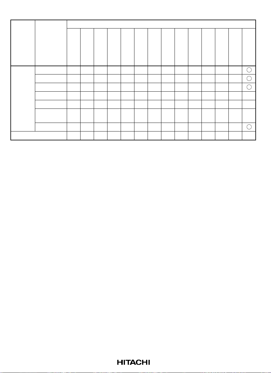
Table 2.2 Combinations of Instructions and Addressing Modes (cont)
Addressing Modes
Function Instruction
@(d:32,ERn)
#xx
Rn
@ERn
@(d:16,ERn)
System TRAPA —————————————
control
Block data transfer —————————————BW
RTE —————————————
SLEEP —————————————
LDC B BWWWW—W—W————
STC —BWWWW—W—W————
ANDC, ORC,
XORC
NOP —————————————
B—————————————
Legend:
B: Byte
W: Word
L: Longword
@–ERn/@ERn+
@aa:8
@aa:16
@aa:24
@aa:32
@(d:8,PC)
@(d:16,PC)
@@aa:8
—
40
Page 61

2.6.3 Table of Instructions Classified by Function
Table 2.3 summarizes the instructions in each functional category. The notation used in table 2.3 is
defined below.
Operation Notation
Rd General register (destination)*
Rs General register (source)*
Rn General register*
ERn General register (32-bit register)
(EAd) Destination operand
(EAs) Source operand
EXR Extended control register
CCR Condition-code register
N N (negative) flag in CCR
Z Z (zero) flag in CCR
V V (overflow) flag in CCR
C C (carry) flag in CCR
PC Program counter
SP Stack pointer
#IMM Immediate data
disp Displacement
+ Addition
– Subtraction
× Multiplication
÷ Division
∧ Logical AND
∨ Logical OR
⊕ Logical exclusive OR
→ Move
¬ NOT (logical complement)
:8/:16/:24/:32 8-, 16-, 24-, or 32-bit length
Note: *General registers include 8-bit registers (R0H to R7H, R0L to R7L), 16-bit registers (R0 to
R7, E0 to E7), and 32-bit registers (ER0 to ER7).
41
Page 62

Table 2.3 Instructions Classified by Function
Type Instruction Size* Function
Data transfer MOV B/W/L (EAs) → Rd, Rs → (Ead)
Moves data between two general registers or between a
general register and memory, or moves immediate data
to a general register.
MOVFPE B Cannot be used in the H8S/2345 Series.
MOVTPE B Cannot be used in the H8S/2345 Series.
POP W/L @SP+ → Rn
Pops a register from the stack. POP.W Rn is identical to
MOV.W @SP+, Rn. POP.L ERn is identical to MOV.L
@SP+, ERn.
PUSH W/L Rn → @–SP
Pushes a register onto the stack. PUSH.W Rn is
identical to MOV.W Rn, @–SP. PUSH.L ERn is identical
to MOV.L ERn, @–SP.
LDM L @SP+ → Rn (register list)
Pops two or more general registers from the stack.
STM L Rn (register list) → @–SP
Pushes two or more general registers onto the stack.
Note: *Size refers to the operand size.
B: Byte
W: Word
L: Longword
42
Page 63

Table 2.3 Instructions Classified by Function (cont)
Type Instruction Size* Function
Arithmetic
operations
Note: *Size refers to the operand size.
B: Byte
W: Word
L: Longword
ADD
SUB
ADDX
SUBX
INC
DEC
ADDS
SUBS
DAA
DAS
MULXU B/W Rd × Rs → Rd
MULXS B/W Rd × Rs → Rd
DIVXU B/W Rd ÷ Rs → Rd
B/W/L Rd ± Rs → Rd, Rd ± #IMM → Rd
Performs addition or subtraction on data in two general
registers, or on immediate data and data in a general
register. (Immediate byte data cannot be subtracted from
byte data in a general register. Use the SUBX or ADD
instruction.)
B Rd ± Rs ± C → Rd, Rd ± #IMM ± C → Rd
Performs addition or subtraction with carry or borrow on
byte data in two general registers, or on immediate data
and data in a general register.
B/W/L Rd ± 1 → Rd, Rd ± 2 → Rd
Increments or decrements a general register by 1 or 2.
(Byte operands can be incremented or decremented by
1 only.)
L Rd ± 1 → Rd, Rd ± 2 → Rd, Rd ± 4 → Rd
Adds or subtracts the value 1, 2, or 4 to or from data in a
32-bit register.
B Rd decimal adjust → Rd
Decimal-adjusts an addition or subtraction result in a
general register by referring to the CCR to produce 4-bit
BCD data.
Performs unsigned multiplication on data in two general
registers: either 8 bits × 8 bits → 16 bits or 16 bits ×
16 bits → 32 bits.
Performs signed multiplication on data in two general
registers: either 8 bits × 8 bits → 16 bits or 16 bits ×
16 bits → 32 bits.
Performs unsigned division on data in two general
registers: either 16 bits ÷ 8 bits → 8-bit quotient and 8-bit
remainder or 32 bits ÷ 16 bits → 16-bit quotient and 16bit remainder.
43
Page 64

Table 2.3 Instructions Classified by Function (cont)
Type Instruction Size* Function
Arithmetic
operations
Note: *Size refers to the operand size.
B: Byte
W: Word
L: Longword
DIVXS B/W Rd ÷ Rs → Rd
Performs signed division on data in two general
registers: either 16 bits ÷ 8 bits → 8-bit quotient and 8-bit
remainder or 32 bits ÷ 16 bits → 16-bit quotient and 16-
bit remainder.
CMP B/W/L Rd – Rs, Rd – #IMM
Compares data in a general register with data in another
general register or with immediate data, and sets CCR
bits according to the result.
NEG B/W/L 0 – Rd → Rd
Takes the two's complement (arithmetic complement) of
data in a general register.
EXTU W/L Rd (zero extension) → Rd
Extends the lower 8 bits of a 16-bit register to word size,
or the lower 16 bits of a 32-bit register to longword size,
by padding with zeros on the left.
EXTS W/L Rd (sign extension) → Rd
Extends the lower 8 bits of a 16-bit register to word size,
or the lower 16 bits of a 32-bit register to longword size,
by extending the sign bit.
TAS B @ERd – 0, 1 → (<bit 7> of @Erd)
Tests memory contents, and sets the most significant bit
(bit 7) to 1.
44
Page 65

Table 2.3 Instructions Classified by Function (cont)
Type Instruction Size* Function
Logic
operations
Shift
operations
Note: *Size refers to the operand size.
B: Byte
W: Word
L: Longword
AND B/W/L Rd ∧ Rs → Rd, Rd ∧ #IMM → Rd
Performs a logical AND operation on a general register
and another general register or immediate data.
OR B/W/L Rd ∨ Rs → Rd, Rd ∨ #IMM → Rd
Performs a logical OR operation on a general register
and another general register or immediate data.
XOR B/W/L Rd ⊕ Rs → Rd, Rd ⊕ #IMM → Rd
Performs a logical exclusive OR operation on a general
register and another general register or immediate data.
NOT B/W/L ¬ (Rd) → (Rd)
Takes the one's complement of general register
contents.
SHAL
SHAR
SHLL
SHLR
ROTL
ROTR
ROTXL
ROTXR
B/W/L Rd (shift) → Rd
Performs an arithmetic shift on general register contents.
1-bit or 2-bit shift is possible.
B/W/L Rd (shift) → Rd
Performs a logical shift on general register contents.
1-bit or 2-bit shift is possible.
B/W/L Rd (rotate) → Rd
Rotates general register contents.
1-bit or 2-bit rotation is possible.
B/W/L Rd (rotate) → Rd
Rotates general register contents through the carry flag.
1-bit or 2-bit rotation is possible.
45
Page 66

Table 2.3 Instructions Classified by Function (cont)
Type Instruction Size* Function
Bitmanipulation
instructions
Note: *Size refers to the operand size.
B: Byte
BSET B 1 → (<bit-No.> of <EAd>)
Sets a specified bit in a general register or memory
operand to 1. The bit number is specified by 3-bit
immediate data or the lower three bits of a general
register.
BCLR B 0 → (<bit-No.> of <EAd>)
Clears a specified bit in a general register or memory
operand to 0. The bit number is specified by 3-bit
immediate data or the lower three bits of a general
register.
BNOT B ¬ (<bit-No.> of <EAd>) → (<bit-No.> of <EAd>)
Inverts a specified bit in a general register or memory
operand. The bit number is specified by 3-bit immediate
data or the lower three bits of a general register.
BTST B ¬ (<bit-No.> of <EAd>) → Z
Tests a specified bit in a general register or memory
operand and sets or clears the Z flag accordingly. The
bit number is specified by 3-bit immediate data or the
lower three bits of a general register.
BAND
BIAND
BOR
BIOR
B
B
B
B
C ∧ (<bit-No.> of <EAd>) → C
ANDs the carry flag with a specified bit in a general
register or memory operand and stores the result in the
carry flag.
C ∧ ¬ (<bit-No.> of <EAd>) → C
ANDs the carry flag with the inverse of a specified bit in
a general register or memory operand and stores the
result in the carry flag.
The bit number is specified by 3-bit immediate data.
C ∨ (<bit-No.> of <EAd>) → C
ORs the carry flag with a specified bit in a general
register or memory operand and stores the result in the
carry flag.
C ∨ ¬ (<bit-No.> of <EAd>) → C
ORs the carry flag with the inverse of a specified bit in a
general register or memory operand and stores the
result in the carry flag.
The bit number is specified by 3-bit immediate data.
46
Page 67

Table 2.3 Instructions Classified by Function (cont)
Type Instruction Size* Function
Bitmanipulation
instructions
Note: *Size refers to the operand size.
B: Byte
BXOR
BIXOR
BLD
BILD
BST
BIST
B
B
B
B
B
B
C ⊕ (<bit-No.> of <EAd>) → C
Exclusive-ORs the carry flag with a specified bit in a
general register or memory operand and stores the
result in the carry flag.
C ⊕ ¬ (<bit-No.> of <EAd>) → C
Exclusive-ORs the carry flag with the inverse of a
specified bit in a general register or memory operand
and stores the result in the carry flag.
The bit number is specified by 3-bit immediate data.
(<bit-No.> of <EAd>) → C
Transfers a specified bit in a general register or memory
operand to the carry flag.
¬ (<bit-No.> of <EAd>) → C
Transfers the inverse of a specified bit in a general
register or memory operand to the carry flag.
The bit number is specified by 3-bit immediate data.
C → (<bit-No.> of <EAd>)
Transfers the carry flag value to a specified bit in a
general register or memory operand.
¬ C → (<bit-No.> of <EAd>)
Transfers the inverse of the carry flag value to a
specified bit in a general register or memory operand.
The bit number is specified by 3-bit immediate data.
47
Page 68

Table 2.3 Instructions Classified by Function (cont)
Type Instruction Size* Function
Branch
instructions
Bcc — Branches to a specified address if a specified condition
is true. The branching conditions are listed below.
Mnemonic Description Condition
BRA(BT) Always (true) Always
BRN(BF) Never (false) Never
BHI High C ∨ Z = 0
BLS Low or same C ∨ Z = 1
BCC(BHS) Carry clear C = 0
BCS(BLO) Carry set (low) C = 1
BNE Not equal Z = 0
BEQ Equal Z = 1
BVC Overflow clear V = 0
BVS Overflow set V = 1
BPL Plus N = 0
BMI Minus N = 1
BGE Greater or equal N ⊕ V = 0
BLT Less than N ⊕ V = 1
BGT Greater than Z∨(N ⊕ V) = 0
BLE Less or equal Z∨(N ⊕ V) = 1
(high or same)
48
JMP — Branches unconditionally to a specified address.
BSR — Branches to a subroutine at a specified address.
JSR — Branches to a subroutine at a specified address.
RTS — Returns from a subroutine
Page 69

Table 2.3 Instructions Classified by Function (cont)
Type Instruction Size* Function
System control TRAPA — Starts trap-instruction exception handling.
instructions
Note: *Size refers to the operand size.
B: Byte
W: Word
RTE — Returns from an exception-handling routine.
SLEEP — Causes a transition to a power-down state.
LDC B/W (EAs) → CCR, (EAs) → EXR
Moves the source operand contents or immediate data
to CCR or EXR. Although CCR and EXR are 8-bit
registers, word-size transfers are performed between
them and memory. The upper 8 bits are valid.
STC B/W CCR → (EAd), EXR → (EAd)
Transfers CCR or EXR contents to a general register or
memory. Although CCR and EXR are 8-bit registers,
word-size transfers are performed between them and
memory. The upper 8 bits are valid.
ANDC B CCR ∧ #IMM → CCR, EXR ∧ #IMM → EXR
Logically ANDs the CCR or EXR contents with
immediate data.
ORC B CCR ∨ #IMM → CCR, EXR ∨ #IMM → EXR
Logically ORs the CCR or EXR contents with immediate
data.
XORC B CCR ⊕ #IMM → CCR, EXR ⊕ #IMM → EXR
Logically exclusive-ORs the CCR or EXR contents with
immediate data.
NOP — PC + 2 → PC
Only increments the program counter.
49
Page 70

Table 2.3 Instructions Classified by Function (cont)
Type Instruction Size Function
Block data
transfer
instruction
EEPMOV.B
EEPMOV.W——
if R4L ≠ 0 then
Repeat @ER5+ → @ER6+
R4L–1 → R4L
Until R4L = 0
else next;
if R4 ≠ 0 then
Repeat @ER5+ → @ER6+
R4–1 → R4
Until R4 = 0
else next;
Transfers a data block according to parameters set in
general registers R4L or R4, ER5, and ER6.
R4L or R4: size of block (bytes)
ER5: starting source address
ER6: starting destination address
Execution of the next instruction begins as soon as the
transfer is completed.
50
Page 71

2.6.4 Basic Instruction Formats
The CPU instructions consist of 2-byte (1-word) units. An instruction consists of an operation
field (op field), a register field (r field), an effective address extension (EA field), and a condition
field (cc).
Figure 2.12 shows examples of instruction formats.
(1) Operation field only
op
(2) Operation field and register fields
op
(3) Operation field, register fields, and effective address extension
op
EA (disp)
(4) Operation field, effective address extension, and condition field
op cc EA (disp) BRA d:16, etc
rn
rn rm
rm
NOP, RTS, etc.
ADD.B Rn, Rm, etc.
MOV.B @(d:16, Rn), Rm, etc.
Figure 2.12 Instruction Formats (Examples)
(1) Operation Field: Indicates the function of the instruction, the addressing mode, and the
operation to be carried out on the operand. The operation field always includes the first four bits of
the instruction. Some instructions have two operation fields.
(2) Register Field: Specifies a general register. Address registers are specified by 3 bits, data
registers by 3 bits or 4 bits. Some instructions have two register fields. Some have no register
field.
(3) Effective Address Extension: Eight, 16, or 32 bits specifying immediate data, an absolute
address, or a displacement.
(4) Condition Field: Specifies the branching condition of Bcc instructions.
51
Page 72

2.7 Addressing Modes and Effective Address Calculation
2.7.1 Addressing Mode
The CPU supports the eight addressing modes listed in table 2.4. Each instruction uses a subset of
these addressing modes. Arithmetic and logic instructions can use the register direct and
immediate modes. Data transfer instructions can use all addressing modes except program-counter
relative and memory indirect. Bit manipulation instructions use register direct, register indirect, or
absolute addressing mode to specify an operand, and register direct (BSET, BCLR, BNOT, and
BTST instructions) or immediate (3-bit) addressing mode to specify a bit number in the operand.
Table 2.4 Addressing Modes
No. Addressing Mode Symbol
1 Register direct Rn
2 Register indirect @ERn
3 Register indirect with displacement @(d:16,ERn)/@(d:32,ERn)
4 Register indirect with post-increment
Register indirect with pre-decrement
5 Absolute address @aa:8/@aa:16/@aa:24/@aa:32
6 Immediate #xx:8/#xx:16/#xx:32
7 Program-counter relative @(d:8,PC)/@(d:16,PC)
8 Memory indirect @@aa:8
@ERn+
@–ERn
(1) Register Direct—Rn: The register field of the instruction specifies an 8-, 16-, or 32-bit
general register containing the operand. R0H to R7H and R0L to R7L can be specified as 8-bit
registers. R0 to R7 and E0 to E7 can be specified as 16-bit registers. ER0 to ER7 can be specified
as 32-bit registers.
(2) Register Indirect—@ERn: The register field of the instruction code specifies an address
register (ERn) which contains the address of the operand on memory. If the address is a program
instruction address, the lower 24 bits are valid and the upper 8 bits are all assumed to be 0 (H'00).
(3) Register Indirect with Displacement—@(d:16, ERn) or @(d:32, ERn): A 16-bit or 32-bit
displacement contained in the instruction is added to an address register (ERn) specified by the
register field of the instruction, and the sum gives the address of a memory operand. A 16-bit
displacement is sign-extended when added.
52
Page 73

(4) Register Indirect with Post-Increment or Pre-Decrement—@ERn+ or @-ERn:
• Register indirect with post-increment—@ERn+
The register field of the instruction code specifies an address register (ERn) which contains the
address of a memory operand. After the operand is accessed, 1, 2, or 4 is added to the address
register contents and the sum is stored in the address register. The value added is 1 for byte
access, 2 for word transfer instruction, or 4 for longword transfer instruction. For word or
longword transfer instruction, the register value should be even.
• Register indirect with pre-decrement—@-ERn
The value 1, 2, or 4 is subtracted from an address register (ERn) specified by the register field
in the instruction code, and the result becomes the address of a memory operand. The result is
also stored in the address register. The value subtracted is 1 for byte access, 2 for word transfer
instruction, or 4 for longword transfer instruction. For word or longword transfer instruction,
the register value should be even.
(5) Absolute Address—@aa:8, @aa:16, @aa:24, or @aa:32: The instruction code contains the
absolute address of a memory operand. The absolute address may be 8 bits long (@aa:8), 16 bits
long (@aa:16), 24 bits long (@aa:24), or 32 bits long (@aa:32).
To access data, the absolute address should be 8 bits (@aa:8), 16 bits (@aa:16), or 32 bits
(@aa:32) long. For an 8-bit absolute address, the upper 24 bits are all assumed to be 1 (H'FFFF).
For a 16-bit absolute address the upper 16 bits are a sign extension. A 32-bit absolute address can
access the entire address space.
A 24-bit absolute address (@aa:24) indicates the address of a program instruction. The upper 8
bits are all assumed to be 0 (H'00).
Table 2.5 indicates the accessible absolute address ranges.
Table 2.5 Absolute Address Access Ranges
Absolute Address Normal Mode
Data address 8 bits (@aa:8) H'FF00 to H'FFFF H'FFFF00 to H'FFFFFF
16 bits (@aa:16) H'0000 to H'FFFF H'000000 to H'007FFF,
32 bits (@aa:32) H'000000 to H'FFFFFF
Program instruction
address
Note: *ZTAT, mask ROM, and ROMless versions only.
24 bits (@aa:24)
*
Advanced Mode
H'FF8000 to H'FFFFFF
53
Page 74

(6) Immediate—#xx:8, #xx:16, or #xx:32: The instruction contains 8-bit (#xx:8), 16-bit
(#xx:16), or 32-bit (#xx:32) immediate data as an operand.
The ADDS, SUBS, INC, and DEC instructions contain immediate data implicitly. Some bit
manipulation instructions contain 3-bit immediate data in the instruction code, specifying a bit
number. The TRAPA instruction contains 2-bit immediate data in its instruction code, specifying a
vector address.
(7) Program-Counter Relative—@(d:8, PC) or @(d:16, PC): This mode is used in the Bcc and
BSR instructions. An 8-bit or 16-bit displacement contained in the instruction is sign-extended and
added to the 24-bit PC contents to generate a branch address. Only the lower 24 bits of this branch
address are valid; the upper 8 bits are all assumed to be 0 (H'00). The PC value to which the
displacement is added is the address of the first byte of the next instruction, so the possible
branching range is –126 to +128 bytes (–63 to +64 words) or –32766 to +32768 bytes (–16383 to
+16384 words) from the branch instruction. The resulting value should be an even number.
(8) Memory Indirect—@@aa:8: This mode can be used by the JMP and JSR instructions. The
instruction code contains an 8-bit absolute address specifying a memory operand. This memory
operand contains a branch address. The upper bits of the absolute address are all assumed to be 0,
so the address range is 0 to 255 (H'0000 to H'00FF in normal mode, H'000000 to H'0000FF in
advanced mode). In normal mode* the memory operand is a word operand and the branch address
is 16 bits long. In advanced mode the memory operand is a longword operand, the first byte of
which is assumed to be all 0 (H'00).
Note that the first part of the address range is also the exception vector area. For further details,
refer to section 4, Exception Handling.
Note: * ZTAT, mask ROM, and ROMless versions only.
54
Page 75
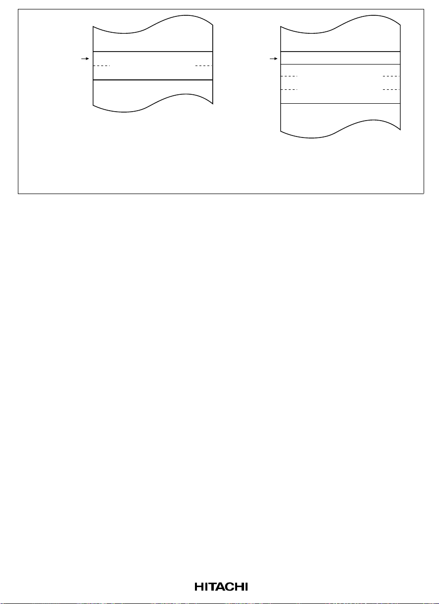
Specified
by @aa:8
Branch address
Specified
by @aa:8
Reserved
Branch address
(a) Normal Mode
Note: * ZTAT, mask ROM, and ROMless versions only.
*
(b) Advanced Mode
Figure 2.13 Branch Address Specification in Memory Indirect Mode
If an odd address is specified in word or longword memory access, or as a branch address, the
least significant bit is regarded as 0, causing data to be accessed or instruction code to be fetched
at the address preceding the specified address. (For further information, see section 2.5.2, Memory
Data Formats.)
2.7.2 Effective Address Calculation
Table 2.6 indicates how effective addresses are calculated in each addressing mode. In normal
mode* the upper 8 bits of the effective address are ignored in order to generate a 16-bit address.
Note: * ZTAT, mask ROM, and ROMless versions only.
55
Page 76

Table 2.6 Effective Address Calculation
Addressing Mode and
No.
Instruction Format
Effective Address
Calculation Effective Address (EA)
1 Register direct (Rn)
op rm rn
2 Register indirect (@ERn)
31 0
General register contents
rop
3 Register indirect with displacement
@(d:16, ERn) or @(d:32, ERn)
31 0
General register contents
op r
disp
31 0
Sign extension disp
4 Register indirect with post-increment or pre-decrement
• Register indirect with post-increment @ERn+
31 0
General register contents
Operand is general register
contents.
31 0
24 23
Don’t
care
31 0
24 23
Don’t
care
31 0
24 23
Don’t
care
op
r
• Register indirect with pre-decrement @–ERn
op
r
56
1, 2, or
4
31 0
General register contents
Operand
Size
Byte
Word
Longword
Value
Added
1
2
4
1, 2, or
4
31 0
24 23
Don’t
care
Page 77

Table 2.6 Effective Address Calculation (cont)
Addressing Mode and
No.
Instruction Format
5 Absolute address
@aa:8
op abs
@aa:16
op
@aa:24
op
@aa:32
op
abs
abs
abs
Effective Address
Calculation Effective Address (EA)
24 23
31 08 7
Don’t
care
31 016 15
Don’t
care
31 0
Don’t
care
31 0
Don’t
care
24 23
24 23
24 23
H'FFFF
Sign
exten-
sion
6 Immediate #xx:8/#xx:16/#xx:32
op
IMM
7 Program-counter relative
@(d:8, PC)/@(d:16, PC)
op disp
23
23
Sign
exten-
sion
PC contents
disp
Operand is immediate data.
0
0
31 0
24 23
Don’t
care
57
Page 78
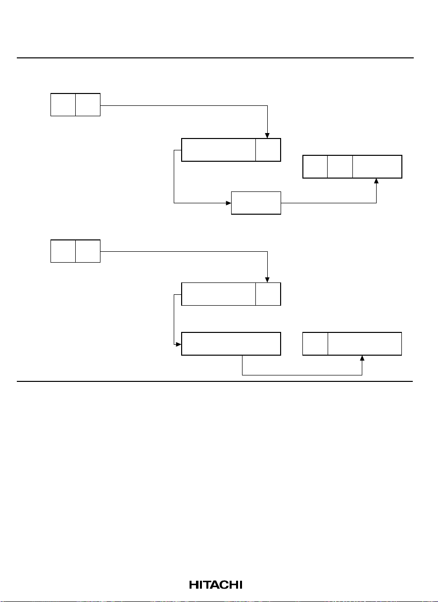
Table 2.6 Effective Address Calculation (cont)
Addressing Mode and
No.
Instruction Format
8 Memory indirect @@aa:8
• Normal mode
op abs
*
• Advanced mode
op abs
Effective Address
Calculation Effective Address (EA)
31 8 7
H'000000
15
Memory
contents
31 8 7
H'000000
abs
abs
0
31 0
24 23
Don’t
H'00
care
0
0
0
16 15
31
Memory contents
Note: *ZTAT, mask ROM, and ROMless versions only.
58
31 0
Don’t
care
24 23
0
Page 79
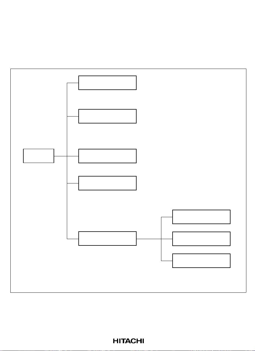
2.8 Processing States
2.8.1 Overview
The CPU has five main processing states: the reset state, exception handling state, program
execution state, bus-released state, and power-down state. Figure 2.14 shows a diagram of the
processing states. Figure 2.15 indicates the state transitions.
Reset state
The CPU and all on-chip supporting modules have been
initialized and are stopped.
Exception-handling
state
A transient state in which the CPU changes the normal
processing flow in response to a reset, interrupt, or trap
instruction.
Processing
states
Note: *The power-down state also includes a medium-speed mode, module stop mode etc.
Program execution
state
The CPU executes program instructions in sequence.
Bus-released state
The external bus has been released in response to a bus
request signal from a bus master other than the CPU.
Sleep mode
Power-down state
CPU operation is stopped
to conserve power.*
Software standby
mode
Hardware standby
mode
Figure 2.14 Processing States
59
Page 80

y
End of bus
request
Bus-released state
End of
exception
handling
Exception-handling state
RES = high
End of bus request
Program execution
Bus
request
Request for
exception
handling
External interrupt
Bus request
state
Interrupt
request
SLEEP
instruction
with
SSBY = 1
SLEEP
instruction
with
SSBY = 0
Sleep mode
Software standby mode
Reset state
Notes: 1.2.From any state except hardware standby mode, a transition to the reset state occurs whenever RES
goes low. A transition can also be made to the reset state when the watchdog timer overflows.
From an
*1
state, a transition to hardware standby mode occurs when STBY goes low.
STBY = high, RES = low
Hardware standby mode
Power-down state
*2
Figure 2.15 State Transitions
2.8.2 Reset State
When the RES input goes low all current processing stops and the CPU enters the reset state. The
CPU enters the power-on reset state when the NMI pin is high, or the manual reset state when the
NMI pin is low. All interrupts are masked in the reset state. Reset exception handling starts when
the RES signal changes from low to high.
The reset state can also be entered by a watchdog timer overflow. For details, refer to section 11,
Watchdog Timer.
60
Page 81

2.8.3 Exception-Handling State
The exception-handling state is a transient state that occurs when the CPU alters the normal
processing flow due to a reset, interrupt, or trap instruction. The CPU fetches a start address
(vector) from the exception vector table and branches to that address.
(1) Types of Exception Handling and Their Priority
Exception handling is performed for traces, resets, interrupts, and trap instructions. Table 2.7
indicates the types of exception handling and their priority. Trap instruction exception handling is
always accepted, in the program execution state.
Exception handling and the stack structure depend on the interrupt control mode set in SYSCR.
Table 2.7 Exception Handling Types and Priority
Priority Type of Exception Detection Timing Start of Exception Handling
High Reset Synchronized with clock Exception handling starts
immediately after a low-to-high
transition at the RES pin, or
when the watchdog timer
overflows.
Trace End of instruction
execution or end of
exception-handling
sequence*
1
Interrupt End of instruction
execution or end of
exception-handling
sequence*
2
Trap instruction When TRAPA instruction
is executed
Low
Notes: 1. Traces are enabled only in interrupt control mode 2. Trace exception-handling is not
executed at the end of the RTE instruction.
2. Interrupts are not detected at the end of the ANDC, ORC, XORC, and LDC instructions,
or immediately after reset exception handling.
3. Trap instruction exception handling is always accepted, in the program execution state.
When the trace (T) bit is set to
1, the trace starts at the end of
the current instruction or current
exception-handling sequence
When an interrupt is requested,
exception handling starts at the
end of the current instruction or
current exception-handling
sequence
Exception handling starts when
a trap (TRAPA) instruction is
executed*
3
61
Page 82

(2) Reset Exception Handling
After the RES pin has gone low and the reset state has been entered, when RES goes high again,
reset exception handling starts. The CPU enters the power-on reset state when the NMI pin is high,
or the manual reset state when the NMI pin is low. When reset exception handling starts the CPU
fetches a start address (vector) from the exception vector table and starts program execution from
that address. All interrupts, including NMI, are disabled during reset exception handling and after
it ends.
(3) Traces
Traces are enabled only in interrupt control mode 2. Trace mode is entered when the T bit of EXR
is set to 1. When trace mode is established, trace exception handling starts at the end of each
instruction.
At the end of a trace exception-handling sequence, the T bit of EXR is cleared to 0 and trace mode
is cleared. Interrupt masks are not affected.
The T bit saved on the stack retains its value of 1, and when the RTE instruction is executed to
return from the trace exception-handling routine, trace mode is entered again. Trace exceptionhandling is not executed at the end of the RTE instruction.
Trace mode is not entered in interrupt control mode 0, regardless of the state of the T bit.
(4) Interrupt Exception Handling and Trap Instruction Exception Handling
When interrupt or trap-instruction exception handling begins, the CPU references the stack pointer
(ER7) and pushes the program counter and other control registers onto the stack. Next, the CPU
alters the settings of the interrupt mask bits in the control registers. Then the CPU fetches a start
address (vector) from the exception vector table and program execution starts from that start
address.
Figure 2.16 shows the stack after exception handling ends.
62
Page 83

Normal mode
*1
SP
(a) Interrupt control mode 0 (b) Interrupt control mode 2
Advanced mode
SP
CCR
*2
CCR
PC
(16 bits)
CCR
PC
(24 bits)
SP
SP
EXR
Reserved
CCR
*2
CCR
PC
(16 bits)
EXR
Reserved
CCR
PC
(24 bits)
*2
*2
(c) Interrupt control mode 0 (d) Interrupt control mode 2
Notes: 1. ZTAT, mask ROM, and ROMless versions only.
2. Ignored when returning.
Figure 2.16 Stack Structure after Exception Handling (Examples)
63
Page 84

2.8.4 Program Execution State
In this state the CPU executes program instructions in sequence.
2.8.5 Bus-Released State
This is a state in which the bus has been released in response to a bus request from a bus master
other than the CPU. While the bus is released, the CPU halts operations.
There is one other bus master in addition to the CPU: the data transfer controller (DTC).
For further details, refer to section 6, Bus Controller.
2.8.6 Power-Down State
The power-down state includes both modes in which the CPU stops operating and modes in which
the CPU does not stop. There are three modes in which the CPU stops operating: sleep mode,
software standby mode, and hardware standby mode. There are also two other power-down
modes: medium-speed mode, and module stop mode. In medium-speed mode the CPU and other
bus masters operate on a medium-speed clock. Module stop mode permits halting of the operation
of individual modules, other than the CPU. For details, refer to section 19, Power-Down State.
(1) Sleep Mode: A transition to sleep mode is made if the SLEEP instruction is executed while
the software standby bit (SSBY) in the standby control register (SBYCR) is cleared to 0. In sleep
mode, CPU operations stop immediately after execution of the SLEEP instruction. The contents of
CPU registers are retained.
(2) Software Standby Mode: A transition to software standby mode is made if the SLEEP
instruction is executed while the SSBY bit in SBYCR is set to 1. In software standby mode, the
CPU and clock halt and all MCU operations stop. As long as a specified voltage is supplied, the
contents of CPU registers and on-chip RAM are retained. The I/O ports also remain in their
existing states.
(3) Hardware Standby Mode: A transition to hardware standby mode is made when the STBY
pin goes low. In hardware standby mode, the CPU and clock halt and all MCU operations stop.
The on-chip supporting modules are reset, but as long as a specified voltage is supplied, on-chip
RAM contents are retained.
64
Page 85
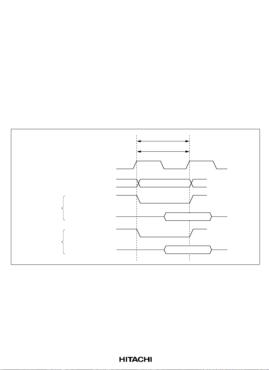
2.9 Basic Timing
2.9.1 Overview
The CPU is driven by a system clock, denoted by the symbol ø. The period from one rising edge
of ø to the next is referred to as a "state." The memory cycle or bus cycle consists of one, two, or
three states. Different methods are used to access on-chip memory, on-chip supporting modules,
and the external address space.
2.9.2 On-Chip Memory (ROM, RAM)
On-chip memory is accessed in one state. The data bus is 16 bits wide, permitting both byte and
word transfer instruction. Figure 2.17 shows the on-chip memory access cycle. Figure 2.18 shows
the pin states.
Bus cycle
T1
ø
Internal address bus
Read
access
Write
access
Internal read signal
Internal data bus
Internal write signal
Internal data bus
Figure 2.17 On-Chip Memory Access Cycle
Address
Read data
Write data
65
Page 86

Bus cycle
g
T1
ø
UnchangedAddress bus
AS
RD
HWR, LWR
Data bus
Hi
High
High
High
h-impedance state
Figure 2.18 Pin States during On-Chip Memory Access
66
Page 87
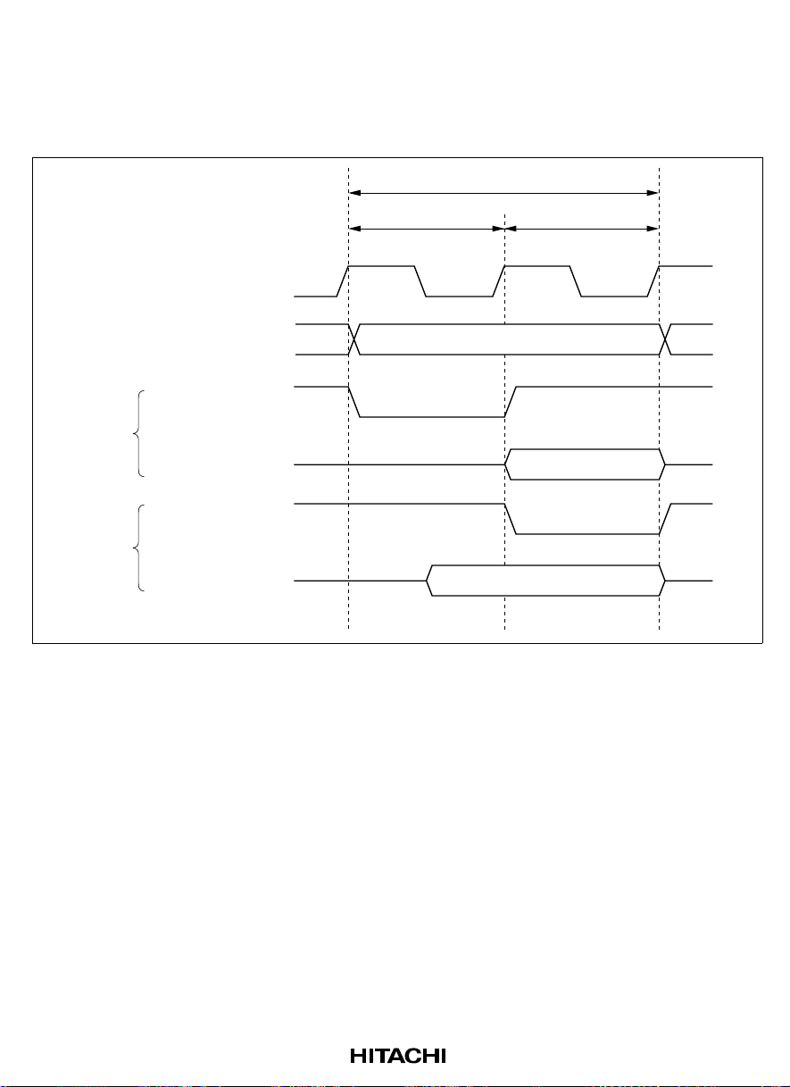
2.9.3 On-Chip Supporting Module Access Timing
The on-chip supporting modules are accessed in two states. The data bus is either 8 bits or 16 bits
wide, depending on the particular internal I/O register being accessed. Figure 2.19 shows the
access timing for the on-chip supporting modules. Figure 2.20 shows the pin states.
Bus cycle
T1 T2
ø
Internal address bus
Internal read signal
Read
access
Internal data bus
Internal write signal
Write
access
Internal data bus
Figure 2.19 On-Chip Supporting Module Access Cycle
Address
Read data
Write data
67
Page 88

Bus cycle
T1 T2
ø
Address bus
AS
RD
HWR, LWR
Data bus
Unchanged
High
High
High
High-impedance state
Figure 2.20 Pin States during On-Chip Supporting Module Access
2.9.4 External Address Space Access Timing
The external address space is accessed with an 8-bit or 16-bit data bus width in a two-state or
three-state bus cycle. In three-state access, wait states can be inserted. For further details, refer to
section 6, Bus Controller.
68
Page 89

Section 3 MCU Operating Modes
3.1 Overview
3.1.1 Operating Mode Selection (F-ZTAT™ Version)
The H8S/2345 Series has eight operating modes (modes 4 to 7, 10, 11, 14 and 15). These modes
are determined by the mode pin (MD2 to MD0) and flash write enable pin (FWE) settings. The
CPU operating mode and initial bus width can be selected as shown in table 3.1.
Table 3.1 lists the MCU operating modes.
Table 3.1 MCU Operating Mode Selection (F-ZTAT™ Version)
External Data
MCU CPU
Operating
Mode FWE MD
0 0000— — — — —
11
210
31
4 1 0 0 Advanced On-chip ROM disabled, Disabled 16 bits 16 bits
51
6 1 0 On-chip ROM enabled,
7 1 Single-chip mode — —
8 1000— — — — —
91
10 1 0 Advanced Boot mode Enabled 8 bits 16 bits
11 1 — —
12 100— — — — —
13 1
14 1 0 Advanced User program mode Enabled 8 bits 16 bits
15 1 — —
MD1MD
2
Operating
Mode Description
0
expanded mode
expanded mode
On-Chip
ROM
Enabled 8 bits 16 bits
Bus
Initial
Width
8 bits 16 bits
Max.
Width
The CPU's architecture allows for 4 Gbytes of address space, but the H8S/2345 Series actually
accesses a maximum of 16 Mbytes.
69
Page 90

Modes 4 to 6 are externally expanded modes that allow access to external memory and peripheral
devices.
The external expansion modes allow switching between 8-bit and 16-bit bus modes. After program
execution starts, an 8-bit or 16-bit address space can be set for each area, depending on the bus
controller setting. If 16-bit access is selected for any one area, 16-bit bus mode is set; if 8-bit
access is selected for all areas, 8-bit bus mode is set.
Note that the functions of each pin depend on the operating mode.
Modes 10, 11, 14, and 15 are boot modes and user program modes in which the flash memory can
be programmed and erased. For details, see section 17, ROM.
The H8S/2345 Series can only be used in modes 4 to 7, 10, 11, 14, and 15. This means that the
flash write enable pin and mode pins must be set to select one of these modes.
Do not change the inputs at the mode pins during operation.
3.1.2 Operating Mode Selection (ZTAT, Mask ROM, and ROMless Versions)
The H8S/2345 Series has seven operating modes (modes 1 to 7). These modes enable selection of
the CPU operating mode, enabling/disabling of on-chip ROM, and the initial bus width setting, by
setting the mode pins (MD2 to MD0).
Table 3.2 lists the MCU operating modes.
70
Page 91

Table 3.2 MCU Operating Mode Selection
MCU CPU
Operating
Mode MD
0 000— — — —
1 1 Normal On-chip ROM disabled,
2* 1 0 On-chip ROM enabled,
3* 1 Single-chip mode —
4 1 0 0 Advanced On-chip ROM disabled,
5 1 8 bits 16 bits
6* 1 0 On-chip ROM enabled,
7* 1 Single-chip mode —
Note: *Not used on ROMless version.
MD1MD
2
Operating
Mode Description
0
expanded mode
expanded mode
expanded mode
expanded mode
On-Chip
ROM
Disabled 8 bits 16 bits
Enabled 8 bits 16 bits
Disabled 16 bits 16 bits
Enabled 8 bits 16 bits
External Data Bus
Initial
Width
Max.
Width
The CPU's architecture allows for 4 Gbytes of address space, but the H8S/2345 Series actually
accesses a maximum of 16 Mbytes.
Modes 1, 2, and 4 to 6 are externally expanded modes that allow access to external memory and
peripheral devices.
The external expansion modes allow switching between 8-bit and 16-bit bus modes. After program
execution starts, an 8-bit or 16-bit address space can be set for each area, depending on the bus
controller setting. If 16-bit access is selected for any one area, 16-bit bus mode is set; if 8-bit
access is selected for all areas, 8-bit bus mode is set.
Note that the functions of each pin depend on the operating mode.
The H8S/2345 Series can be used only in modes 1 to 7. This means that the mode pins must be
set to select one of these modes. Do not change the inputs at the mode pins during operation.
71
Page 92

3.1.3 Register Configuration
The H8S/2345 Series has a mode control register (MDCR) that indicates the inputs at the mode
pins (MD2 to MD0), and a system control register (SYSCR) and a system control register 2
(SYSCR2)*2 that control the operation of the H8S/2345 Series. Table 3.3 summarizes these
registers.
Table 3.3 MCU Registers
Name Abbreviation R/W Initial Value Address*
Mode control register MDCR R Undetermined H'FF3B
System control register SYSCR R/W H'01 H'FF39
System control register 2*2SYSCR2 R/W H'00 H'FF42
Notes: 1. Lower 16 bits of the address.
2. The SYSCR2 register can only be used in the F-ZTAT version. In the ZTAT, mask
ROM, and ROMless versions, this register cannot be written to and will return an
undefined value of read.
1
3.2 Register Descriptions
3.2.1 Mode Control Register (MDCR)
Bit
Initial value
R/W
Note: * Determined by pins MD
7
:
—
1
:
—
:
MDCR is an 8-bit read-only register that indicates the current operating mode of the H8S/2345
Series.
6
—
0
—
to MD0.
2
—
—
5
0
—
—
4
0
—
—
3
0
2
MDS2
—*
R
1
MDS1
—*
R
0
MDS0
—*
R
Bit 7—Reserved: Read-only bit, always read as 1.
Bits 6 to 3—Reserved: Read-only bits, always read as 0.
Bits 2 to 0—Mode Select 2 to 0 (MDS2 to MDS0): These bits indicate the input levels at pins
MD2 to MD0 (the current operating mode). Bits MDS2 to MDS0 correspond to MD2 to MD0.
MDS2 to MDS0 are read-only bits-they cannot be written to. The mode pin (MD2 to MD0) input
levels are latched into these bits when MDCR is read. These latches are canceled by a power-on
reset, but are retained after a manual reset.
72
Page 93

3.2.2 System Control Register (SYSCR)
Bit
Initial value
R/W
7
:
—
0
:
R/W
:
6
—
0
R/W
5
INTM1
0
R/W
4
INTM0
0
R/W
3
NMIEG
0
R/W
2
—
0
R/W
1
—
0
R/W
0
RAME
1
R/W
Bits 7 and 6—Reserved: Only 0 should be written to these bits.
Bits 5 and 4—Interrupt Control Mode 1 and 0 (INTM1, INTM0): These bits select the control
mode of the interrupt controller. For details of the interrupt control modes, see section 5.4.1,
Interrupt Control Modes and Interrupt Operation.
Bit 5 Bit 4
INTM1 INTM0 Control Mode Description
0 0 0 Control of interrupts by I bit (Initial value)
1 — Setting prohibited
1 0 2 Control of interrupts by I2 to I0 bits and IPR
1 — Setting prohibited
Interrupt
Bit 3—NMI Edge Select (NMIEG): Selects the valid edge of the NMI interrupt input.
Bit 3
NMIEG Description
0 An interrupt is requested at the falling edge of NMI input (Initial value)
1 An interrupt is requested at the rising edge of NMI input
Bits 2 and 1—Reserved: Only 0 should be written to these bits.
Bit 0—RAM Enable (RAME): Enables or disables the on-chip RAM. The RAME bit is
initialized when the reset status is released. It is not initialized in software standby mode.
Bit 0
RAME Description
0 On-chip RAM is disabled
1 On-chip RAM is enabled (Initial value)
73
Page 94

3.2.3 System Control Register 2 (SYSCR2) (F-ZTAT Version Only)
Bit:76543210
— — — — FLSHE — — —
Initial value : 0 0 0 0 0 0 0 0
R/W : — — — — R/W — — —
SYSCR2 is an 8-bit readable/writable register that performs on-chip flash memory control.
SYSCR2 is initialized to H'00 by a reset and in hardware standby mode.
SYSCR2 can only be accessed in the F-ZTAT version. In other versions, this register cannot be
written to and will return an undefined value if read.
Bits 7 to 4—Reserved: Read-only bits, always read as 0.
Bit 3—Flash Memory Control Register Enable (FLSHE): Controls CPU access to the flash
memory control registers (FLMCR1, FLMCR2, EBR1, and EBR2). For details, see section 17,
ROM.
Bit 3
FLSHE Description
0 Flash control registers are not selected for addresses H'FFFFC8 to H'FFFFCB
(Initial value)
1 Flash control registers are selected for addresses H'FFFFC8 to H'FFFFCB
Bits 2 to 0—Reserved: Read-only bits, always read as 0.
74
Page 95

3.3 Operating Mode Descriptions
3.3.1 Mode 1 (ZTAT, Mask ROM, and ROMless Versions Only)
The CPU can access a 64-kbyte address space in normal mode. The on-chip ROM is disabled, and
8-bit bus mode is set, immediately after a reset.
Ports B and C function as an address bus, port D functions as a data bus, and part of port F carries
bus control signals. However, note that if 16-bit access is designated by the bus controller, the bus
mode switches to 16 bits and port E becomes a data bus.
1
3.3.2 Mode 2
The CPU can access a 64-kbyte address space in normal mode. The on-chip ROM is enabled, and
8-bit bus mode is set. immediately after a reset.
Ports B and C function as input ports immediately after a reset. They can each be set to output
addresses by setting the corresponding bits in the data direction register (DDR) to 1. Port D
functions as a data bus, and part of port F carries bus control signals. However, note that if 16-bit
access is designated by the bus controller, the bus mode switches to 16 bits and port E becomes a
data bus.
The amount of on-chip ROM that can be used is limited to 56 kbytes.
*
(ZTAT and Mask ROM Versions Only)
1
3.3.3 Mode 3
*
(ZTAT and Mask ROM Versions Only)
The CPU can access a 64-kbyte address space in normal mode. The on-chip ROM is enabled, but
external addresses cannot be accessed.
All I/O ports are available for use as input-output ports.
The amount of on-chip ROM that can be used is limited to 56 kbytes.
2
3.3.4 Mode 4
*
The CPU can access a 16-Mbyte address space in advanced mode. The on-chip ROM is disabled.
Pins P13 to P10, ports A, B and C function as an address bus, ports D and E function as a data bus,
and part of port F carries bus control signals. Pins P13 to P10 function as inputs immediately after a
reset. Each of these pins can be set to output addresses by setting the corresponding bit in the data
direction register (DDR) to 1.
The initial bus mode after a reset is 16 bits, with 16-bit access to all areas. However, note that if
8-bit access is designated by the bus controller for all areas, the bus mode switches to 8 bits.
75
Page 96

2
3.3.5 Mode 5
*
The CPU can access a 16-Mbyte address space in advanced mode. The on-chip ROM is disabled.
Pins P13 to P10, ports A, B and C function as an address bus, port D function as a data bus, and
part of port F carries bus control signals. Pins P13 to P10 function as inputs immediately after a
reset. They can each be set to output addresses by setting the corresponding bits in the data
direction register (DDR) to 1.
The initial bus mode after a reset is 8 bits, with 8-bit access to all areas. However, note that if at
least one area is designated for 16-bit access by the bus controller, the bus mode switches to 16
bits and port E becomes a data bus.
1
3.3.6 Mode 6
*
The CPU can access a 16-Mbyte address space in advanced mode. The on-chip ROM is enabled.
Pins P13 to P10, ports A, B and C function as input ports immediately after a reset. They can each
be set to output addresses by setting the corresponding bits in the data direction register (DDR) to
1. Port D functions as a data bus, and part of port F carries bus control signals.
The initial bus mode after a reset is 8 bits, with 8-bit access to all areas. However, if any area is
designated as 16-bit access space by the bus controller, 16-bit bus mode is set and port E becomes
a data bus.
1
3.3.7 Mode 7
*
The CPU can access a 16-Mbyte address space in advanced mode. The on-chip ROM is enabled,
but external addresses cannot be accessed.
All I/O ports are available for use as input-output ports.
Notes: 1. Not used on ROMless version.
2. The upper address pins (A23 to A20) cannot be used as outputs in modes 4 or 5
immediately after a reset. To use the upper address pins (A23 to A20) as outputs, it is
necessary to first set the corresponding bits in the port 1 data direction register
(P1DDR) to 1.
3.3.8 Modes 8 and 9 (F-ZTAT Version Only)
Modes 8 and 9 are not supported in the H8S/2345 Series, and must not be set.
76
Page 97

3.3.9 Mode 10 (F-ZTAT Version Only)
This is a flash memory boot mode. For details, see section 17, ROM.
MCU operation is the same as in mode 6.
3.3.10 Mode 11 (F-ZTAT Version Only)
This is a flash memory boot mode. For details, see section 17, ROM.
MCU operation is the same as in mode 7.
3.3.11 Modes 12 and 13 (F-ZTAT Version Only)
Modes 12 and 13 are not supported in the H8S/2345 Series, and must not be set.
3.3.12 Mode 14 (F-ZTAT Version Only)
This is a flash memory user program mode. For details, see section 17, ROM.
MCU operation is the same as in mode 6.
3.3.13 Mode 15 (F-ZTAT Version Only)
This is a flash memory user program mode. For details, see section 17, ROM.
MCU operation is the same as in mode 7.
77
Page 98

3.4 Pin Functions in Each Operating Mode
The pin functions of ports 1 and A to F vary depending on the operating mode. Table 3.3 shows
their functions in each operating mode.
Table 3.3 Pin Functions in Each Mode
3
Mode 6
Mode 10
Mode 14
/T/A P
Port Mode 1
1
Port 1 P13 to P10P
*
/T P
2
*
Mode 2
1
*
/T P
3
*
Mode 3
1
*
/T P
3
*
Mode 4 Mode 5
1
*
/T/A P
1
*
Port A PA3 to PA0PP P AAP
1
Port B A P
Port C A P
*
/AP AAP
1
*
/AP AAP
*
*
*
1
*
/T/A P
1
*
/A P
1
*
/A P
1
*
/A P
4
4
Port D D D P D D D P
Port E P
Port F PF
7
1
*
/D P
P/C
1
*
1
*
/D P P/D P
P/C
1
*
1
*
P
/C P/C
1
*
/D P
1
*
P/C
1
*
1
*
/D P
1
*
P/C
PF6 to PF3CC P CCC P
PF2 to PF0P
1
*
/C P
1
*
/C P
1
*
/C P
1
*
/C P
1
*
/C
Legend
P: I/O port
T: Timer I/O
A: Address bus output
D: Data bus I/O
C: Control signals, clock I/O
Notes: 1. After reset
2. Not used on F-ZTAT.
3. Not used on ROMless version.
4. Applies to F-ZTAT version only.
Mode 7
Mode 11
Mode 15
1
*
/T
1
*
P
/C
3
*
4
*
4
*
78
Page 99

3.5 Memory Map in Each Operating Mode
Memory maps for the H8S/2345, H8S/2344, H8S/2343, H8S/2341, and H8S/2340 are shown in
figure 3.1 to figure 3.5.
The address space is 64 kbytes in modes 1 to 3 (normal modes)*, and 16 Mbytes in modes 4 to 7,
10, 11, 14, and 15 (advanced modes). The on-chip ROM capacity of the H8S/2345 is 128 kbytes,
that of the H8S/2344 96 kbytes, and that of the H8S/2343 64 kbytes. However, only 56 kbytes are
available in modes 2 and 3 (normal modes)*.
The address space is divided into eight areas for modes 4 to 6, 10, and 14. For details, see section
6, Bus Controller.
Note: * Not available on F-ZTAT version.
79
Page 100

Mode 1
*2
(normal expanded mode
with on-chip ROM disabled)
(normal expanded mode
with on-chip ROM enabled)
Mode 2
*2
(normal single-chip mode)
H'0000 H'0000 H'0000
Mode 3
*2
External address
On-chip ROM
On-chip ROM
space
H'DFFF
H'E000
External address
H'DFFF
space
H'EC00
On-chip RAM
*1
H'EC00
On-chip RAM
H'EC00
*1
On-chip RAM
H'FBFF
H'FC00
H'FE40 H'FE40
H'FF08 H'FF08
H'FF28 H'FF28 H'FF28
H'FFFF
External address
space
Internal I/O registers
External address
space
Internal I/O registers
H'FC00
H'FFFF
External address
space
Internal I/O registers
External address
space
Internal I/O registers Internal I/O registers
H'FE40
H'FF07
H'FFFF
Internal I/O registers
Notes: 1. External addresses can be accessed by clearing the RAME bit in SYSCR to 0.
2. Not available on F-ZTAT version.
80
Figure 3.1 Memory Map in Each Operating Mode in the H8S/2345
 Loading...