

Page 1
NOVEMBER, 1999 Prepared by: ALVIE RODGERS C.E.T.
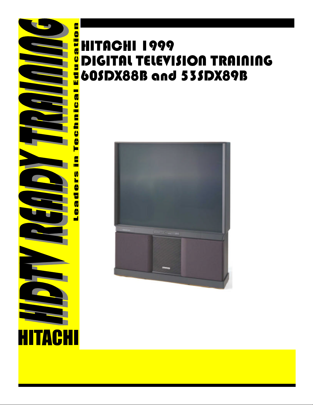
This training package is geared specifically to the 60SDX88B progressive scan HDTV capable set. The necessary understanding that the 60SDX88B requires a Set-Top-Box to receive SDTV and HDTV signals is important. The 60SDX88B does NOT have a DM-1
module. This module is built into the 61HDX98B which allows this set to receive all
ATSC formats as well as Direct TV, NTSC, SDTV or HDTV.
The 60SDX88B has a built in FLEX converter that translates any input into either 480P for
NTSC or SDTV and/or 1080I for HDTV. It does have Component Inputs.
The Power Supplies are the same for either set.
The Deflection circuit is very similar between the two sets.
The Signal PWB is very similar between the two sets, minus the differences mentioned
above.
Digital Convergence is the same between the two sets.
61HDX98B is a DP-85 chassis with a 16X9 aspect screen.
60SDX88B and the 50SDX89B is a DP-86 chassis with a 3X4 aspect screen.
CONTENTS... 1999 DP-86 HDTV Ready Projection Television Information
Page 2
DP-86 BLANK PAGE “NOTES”
BLANK PAGE
Page 3
60SDX88B DP86 CHASSIS TRAINING and INFORMATION
CONTENTS
SECTION PAGE
1): GENERAL BLOCK DIAGRAMS, SECTION:
• Power Supply Block Diagram --------------------------------------------------------------- 01-01
• AV Selector Block Diagram ----------------------------------------------------------------- 01-02
• Signal Processing Block Diagram ---------------------------------------------------------- 01-03
• System Control Block Diagram ------------------------------------------------------------- 01-04
• 2H Video Block Diagram -------------------------------------------------------------------- 01-05
• AV Selector Block Explanation ------------------------------------------------------------- 01-06
• Deflection Circuit Block Diagram ---------------------------------------------------------- 01-07
• CRT Block Diagram -------------------------------------------------------------------------- 01-08
• Audio Output Block Diagram --------------------------------------------------------------- 01-09
• Rear Panel Diagram -------------------------------------------------------------------------- 01-10
• 16X9 Displayed on 4X3 Screen ------------------------------------------------------------- 01-11
2): POWER SUPPLY INFORMATION, SECTION:
• Sub Power Supply SHUT DOWN Block Diagram --------------------------------------- 02-01
• Sub Power Supply SHUT DOWN Circuit Diagram -------------------------------------- 02-02
• Sub Power Supply Visual Trouble Shooting LED's Diagram -------------------------- 02-03
• Sub Power Supply Distribution Diagram -------------------------------------------------- 02-04
• Deflection and High Voltage Power Supply SHUT DOWN Block Diagram --------- 02-05
• Deflection and High Voltage Power Supply SHUT DOWN Circuit Diagram -------- 02-06
• Deflection Power Supply Visual Trouble Shooting LED's Diagram ------------------ 02-07
• Deflection Power Supply Distribution Diagram ------------------------------------------ 02-08
3): HORIZONTAL DRIVE, SECTION:
• Horizontal Drive Circuit Diagram --------------------------------------------------------- 03-01
4): VIDEO SIGNAL INFORMATION:
• Video Signal Main and Terminal Circuit Diagram -------------------------------------- 04-01
• ABL Circuit Diagram ------------------------------------------------------------------------- 04-02
• Horizontal and Vertical SWEEP LOSS DETECTION Circuit ------------------------ 04-03
5): AUDIO CIRCUIT INFORMATION:
• Audio Signal Main and Terminal Board Circuit Diagram ----------------------------- 05-01
• Audio SURROUND Board Circuit Diagram ---------------------------------------------- 05-02
• Front Left & Right Graphic EQ Circuit Diagram -------------------------------------- 05-03
• Center Graphic EQ Circuit Diagram ------------------------------------------------------ 05-04
• Audio and Video MUTE Circuit Diagram ------------------------------------------------ 05-05
• Audio MUTE Surround Board Circuit Diagram ----------------------------------------- 05-06
• Audio MUTE Audio Output Board Circuit Diagram ------------------------------------ 05-07
6): DIGITAL CONVERGENCE CIRCUIT INFORMATION:
• Digital Convergence INTER-CONNECTION Diagram -------------------------------- 06-01
• Digital Convergence OVERLAY DIMENSIONS Information ------------------------ 06-02
• Digital Convergence REMOTE CONTROL Button Identification ------------------- 06-03
CONTENTS PAGE (A-1)
Page 4
60SDX88B DP86 CHASSIS TRAINING and INFORMATION
CONTENTS
SECTION PAGE
7): MICROPROCESSOR
• Microprocessor Port Block Diagram ..........................................................................07-01
• Microprocessor Data Communications Block Diagram .............................................07-02
8): PWB INFORMATION
• Signal PWB ...................................................................................................................08-01
• Deflection PWB ............................................................................................................08-02
• Control PWB ................................................................................................................08-03
• CRT PWB .....................................................................................................................08-04
• SUB POWER PWB ......................................................................................................08-05
9): MISCELLANEOUS INFORMATION
• Flex Converter Information and Diagram ....................................................................09-01
• 60SDX88B Component and Parts Identification ......................................................09-02
• Overlay Part Numbers Diagram ..................................................................................09-04
• 53SBX89B Component Identification ........................................................................09-05
CONTENTS PAGE (A-2)
Page 5

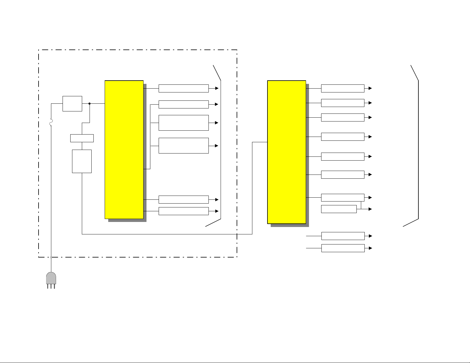
BLOCK DIAGRAM EXPLANATION POWER SUPPLY BLOCK
The 61HDX98B utilizes two switching power supplies.
DP-85's stand by switching mode operation is different
from AP-7X and 8X chassis's. Switching frequency of
AP-7X and 8X chassis is dropped to 20kHz during
stand by mode. But the DP-85's power supply is not
dropped during stand by mode. DP-85's is operated
about 100kHz.
Normally Power Supply switching is operated as following.
T901: 25- 56 kHz (Normal)
100-200 kHz (Stand by)
TP91 30- 53 kHz (normal)
POWER SUPPLY UTILIZED FOR THE DIGITAL AND SIGNAL CIRCUITS:
(Sub Power Supply PWB)
This supplies power primarily to the Digital circuits, i.
e. DM-1 module. This supply runs anytime the set is
plugged into an AC outlet.
The voltages produced are;
• +33V,
• Power for the Satellite dish which is switched be-
tween 13V and 19V dependant upon the channel
being received.
• Stand By 12V also called A12V
• TV9V
• TV5V
• 3.3V
• -5V
POWER SUPPLY UTILIZED FOR THE DEFLECTION, AUDIO and DIGITAL CONVERGENCE CIRCUITS: (Deflection PWB)
This supply only operates when the set is turned ON.
When the ON command is received from the DM-1
module, relay S-901 energizes and delivers AC to the
main bridge rectifier D903 located on the Sub Power
Supply PWB.
This supplies power primarily to the Deflection circuit
for the collector of the High Voltage generation circuit
and the collector of the Deflection Output transistor.
Also, the Convergence output amps and the Audio
output amps derive their voltages from here as well.
The voltages produced are;
• +130V used for Deflection and High Voltage cir-
cuits.
• 220V used for the collectors of the R, G, B drivers
on the CRT PWB and the Velocity Modulation
circuits.
• 6.3V to drive the CRT Heaters.
• +28V for the Convergence, Velocity modulation
and Audio Out circuit.
• +13V for Vertical.
• -13V for Vertical and also converted down to
the –5V for the Digital Convergence Unit.
The TV9V supply generated from the Power Supply
for Digital listed above, is regulated down to +5V for
the Digital Convergence Unit and the A12V for the
Power Supply for Digital is used as a switched On/Off
for the Deflection Vcc by the Rainforest IC.
Page 01-01
Page 6
DP86 POWER SUPPLY BLOCK DIAGRAM
Fuse
Line
Filter
Relay
Line
Filter
R
POWER SUB
P.W.B.
STAND BY
35V
I901
Sub
Switching
Regulator
EE42
24.5V
R/F 28V
C21V
+33VS Reg
A12V Sw. Reg.
9V Sw. Reg.
TV9V
5V Sw. Reg.
TV5V
28V
21V
To Signal Block
POWER DEFLECTION
SWITCHED
IP01
Main
Switching
Regulator
EE49
P.W.B.
(130V) Reg
220V
6.3V
+28V
-28V
+13V Reg.
-13V Sw. Reg.
-5V Reg.
Def. +B V1&V2
CRT &
Vm Out
Heater
Convergence
Velocity Mod.
Convergence
Vertical
Vertical (M13)
DCU
Block
To Deflection
AC108-
PAGE 01-02
132V/
60Hz.
AC Inlet Type
+5V Reg.TV9V
DCU
HVcc12VA12V
Page 7

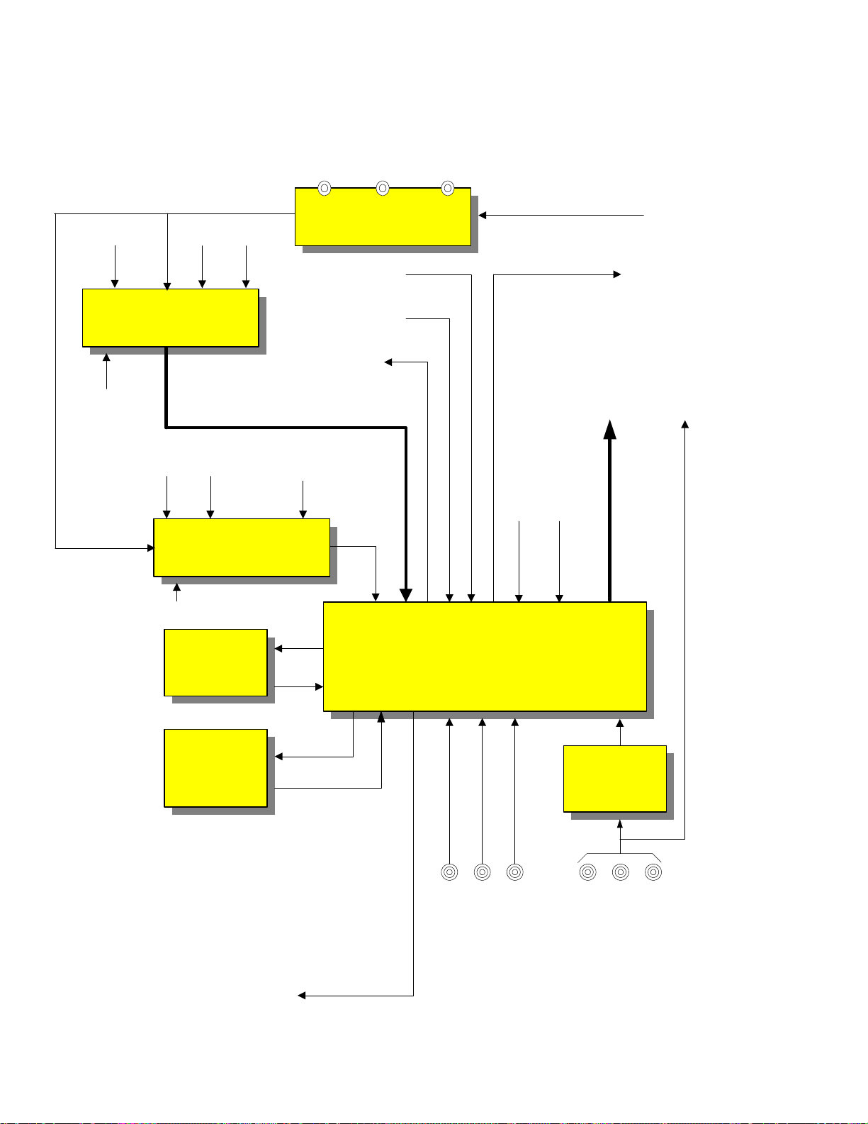
BLOCK DIAGRAM EXPLANATION FRONT END
The 61HDX98B utilizes a non-repairable Front End
Assembly called the DM-1 Module. This module contains the main System control center, NTSC Front
End, Direct TV Receiver and ATSC Tuner. The block
diagram indicates the internal blocks contained within
the Front End Assembly, hear after called the DM-1.
Starting counterclockwise from the upper left.
SATELLITE:
This represents the Direct TV satellite dish connection
to the back of the set.
SATELLITE TUNER/IF:
This is the internal IRD, (Integrated Receiver and Decoder). This receives the satellite signal from the LNB
(Low Noise Block) located on the Dish. This block
converts the signal to a usable signal for decoding.
SATELLITE CARD and SATELLITE LINK
BLOCK:
To receive Direct TV signals, the customer is required
to insert an active Security Card into the back of the
set. This care contains a programmable chip that contains the consumer’s information and the channels that
the consumer is allowed to receive. Also, this card is
used when billing information is retrieved by Direct
TV.
LINK/MIX:
This block passes the particular signal that the customer has decided to view on screen. Either the Direct
TV signal or the ATSC tuner.
TERRESTRIAL:
This indicates the outside antenna the consumer has
erected to receive NTSC signals as well as ATSC signals.
CABLE:
This is the input from the consumer’s cable signal.
HD/NTSC TUNER/IF SPLITTER:
This block receives the Terrestrial signal and dependant upon which source the consumer has decided to
view, processes the signal through the appropriate
tuner.
• HD: Receives the Terrestrial Signal and routes it
to the ATSC tuner. This tuner is capable of receiving all 18 ATSC formats.
• NTSC: Receives the Terrestrial Signal and route
it to the NTSC Tuner.
• The NTSC signal is routed out of this block on the
line labeled Composite Video to the Signal Selector IC which selects the appropriate signal according to the consumer’s choice. Either Tuner,
AVX1, 2 or 3 and/or S-In 1,2 or 3.
• The NTSC audio IF signal is routed to the MTS
STEREO DECODER.
• SPLITTER:
• The splitter routes the NTSC signal out to the RF
Out PinP Tuner path to the PinP Tuner.
MTS STEREO DECODER:
Decodes the NTSC Audio IF signal an decodes it into
Left Total and Right Total. This signal is routed to the
Dolby® Pro-Logic decoder.
HDTV LINK:
This block routs the ATSC signal received by the
ATSC tuner to the Link Mix.
NTSC YUV A/D:
This block receives the NTSC luminance and chroma
signals and converters them to a digital signal to be
utilized by the MPEG VIDEO decoder.
FROM MAIN MICRO:
This is communication in and out for the SubMicroprocessor. Information such as the Selector IC
selection, power on/off commands, etc.., are routed
from the ARM/Transport or Main Microprocessor section.
SD-A/V:
This is the output of the AC-3 digital audio to be used
by an off board AC-3 decoder.
MODEM:
Direct TV polls the Direct TV receiver section through
the customer’s phone lines and determines such things
as Pay for View authorization, customer’s information, Card authorization and billing information.
ARM/TRANSPORT:
The Arm/Transport block receives all signals from Direct TV, ATSC. It also receives the Infrared remote control signals, Front panel Key data, and Slave Microprocessor information. This is the Main Microprocessor section of the DM-1 module. Dynamic RAM and ROM information is processed from Soft ward load into ROM
and determines the state of the Television. Information
from ATSC and/or Direct TV is routed to the MPEG
VIDEO DECODER.
Page 01-03
Page 8

BLOCK DIAGRAM EXPLANATION FRONT END
MPEG VIDEO DECODER, NTSC UPCONVERSION, OSD:
What ever signal is requested by the consumer as the
source for viewing is processed through this block and is
output to the YUV D/As.
YUV/DAs:
This block takes the digital signals provided to it and
converts them to an analog signal which is usable by the
signal processing circuits.
All signals are routed out through the line labeled 2.14
YUV/YIQ, (NTSC Signal up converted to 480P or 2.14
HYPBPR which is the HDTV output as 1080I.
MPEG/AC-3 AUDIO DECODER:
This block processes the audio component from the
ARM/TRANSPORT or the block A/Ds AUDIO, which
is the NTSC audio processed by the Pro Logic decoding
circuit, labeled as 5.1, (Front Left, Front Right, Center,
Rear Left and Rear Right + Sub Woofer audio also called
LFE. Then this block processes the signal and outputs all
audio to the Audio D/As.
AUDIO D/As:
This block is the Digital to Analog converter which converts the digital audio signal sent to it by the ARM/
TRANSPORT block and converts it to a usable analog
signal to be processed by the audio output section.
The audio labeling is comprised of the following:
L/R = Audio Front Left and Right
LS/RS = Rear or Surround audio Left and Right
C/LFE = C for Center and LFE for Sub Woofer, also
called Low Frequency Effects.
Page 01-04
Page 9
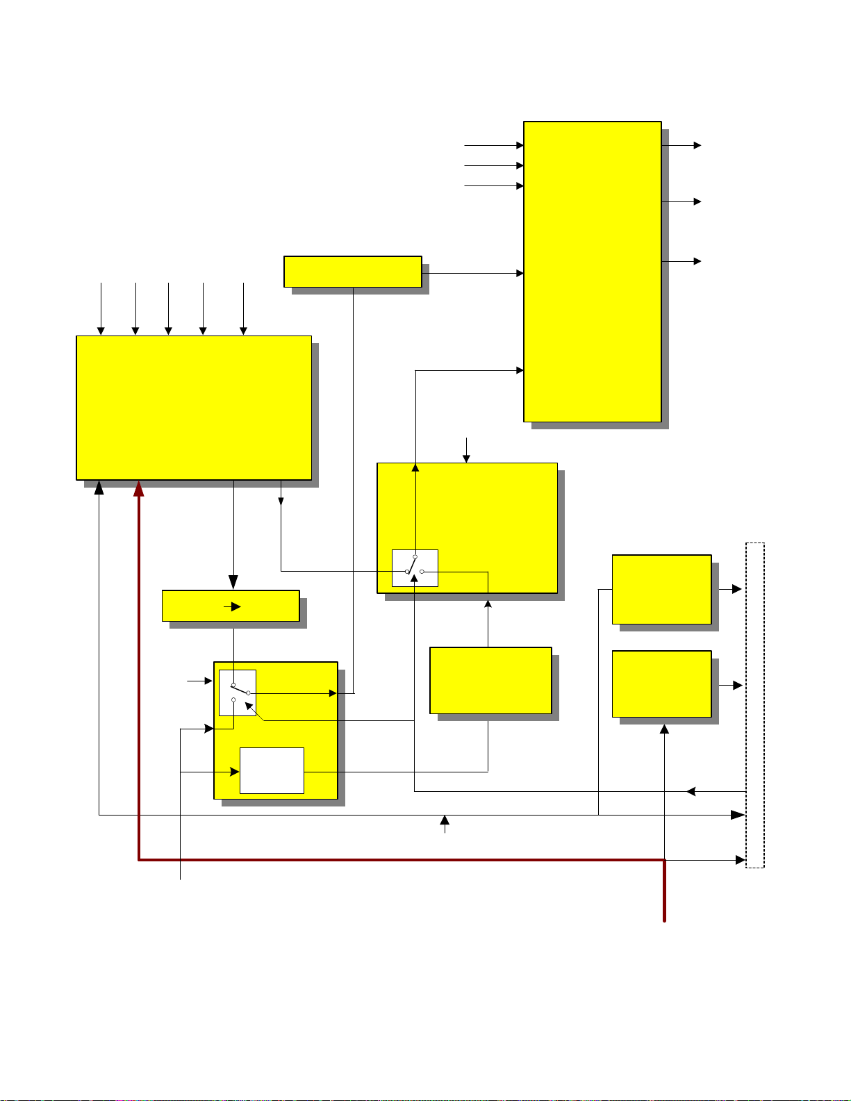
A/V SELECTOR BLOCK DP85 CHASSIS
TERMINAL P.W.B.
Antenna
A
Out to
Converter
Antenna
B
VT+33V
Main
Tuner U002
Lock
Clock
Data
Enable
+5V +9V
Comp. Video (Main) R/L (Main)
+5V +9V
Tuner U003
VT+33V
C/V
Det.
RF
Antenna
Switch Box
Video 4 V4, S4, L/R4
PinP Video and MonoAudio
Selected L/R
(NTSC Main Audio)
Lock/Clock
Data/Enable
Video
PinP
Mono
C Video
C/V Det
PinP
9V
AUDIO/VIDEO
SELECTOR
TA8851BN
Video D YC
To 3DYC
I2C
Ant
From Micro
PinP Video
to PinP Unit
YUV
2 Line
Y/C
for PinP
PinP L/R Out
To Audio Out PWB
PinP V
PinP YC
Video One In
Video Two In
V1 S1 L/R1
V2 S2 L/R2
Video Three In
V3 S3 L/R3
YUV Det
C/V
Det.
YUV
Y
CR/PR
CB/PB
YUV In
480I/480P/1080I
PAGE 01-05
Page 10

BLOCK DIAGRAM EXPLANATION A/V SELECTOR
C. VIDEO (MAIN) and R/L (AUDIO MAIN):
NTSC Video and NTSC Audio is routed from the
DM-1 Block diagram. They are shown in the Block
Diagram as one line, but they are separate signals.
Anytime a signal is routed from the DM-1 or going to
the DM-1 module, they must be sent through a DM-1
I/F block. This block reduces the noise by a noise cancellation process. This process uses the output of a
comparator and routes the output back to the negative
input to subtract the noise. It also level shifts the signal
to make it useable by the circuit to which it is routed.
DM-1 I/F BA4558:
This is the noise cancellation and level shift block.
AUDIO/VIDEO SELECTOR TA8851BN:
This is the selector IC. Dependant upon the customer’s
viewing preference, the DM-1 will communicate via
I2C bus communications and select the NTSC signal
which is sent to the demodulator. The demodulator
prepares the NTSC signal for the DM-1 module.
This IC selects the following inputs;
Main tuner
Video One, Two or Three
S-In One, Two or Three
PinP Video and Audio outputs. This can be any of the
input provided above except the PinP has it’s own
tuner.
Note: PinP isn’t available when the customer has selected Direct TV or ATSC as it’s source. This is because, as will be shown later, the PinP Video is super
exposed upon the NTSC video only.
Any video source selected for the Main picture will be
routed to the 3D Y/C module.
Note: There are NO Component inputs on this set.
Page 01-06
Page 11
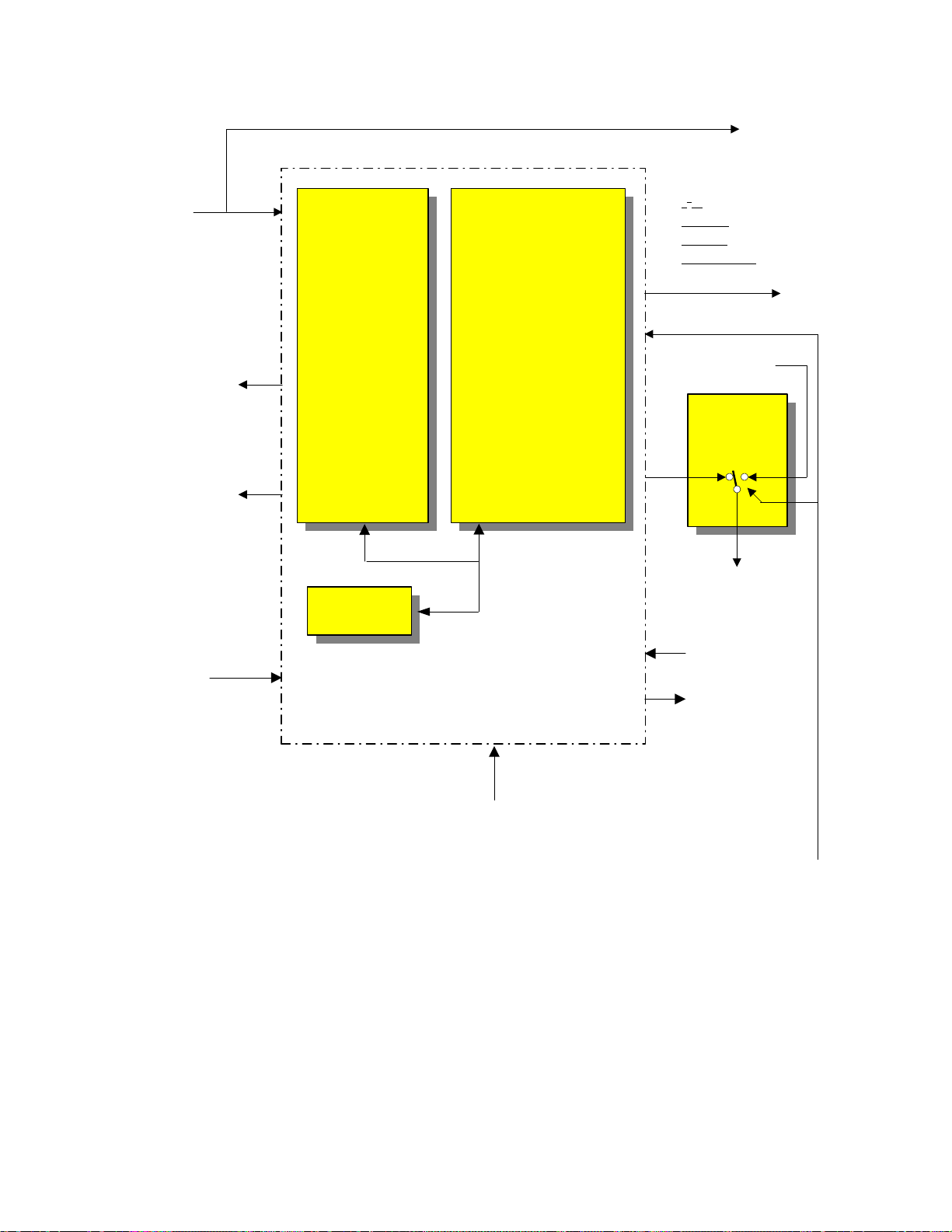
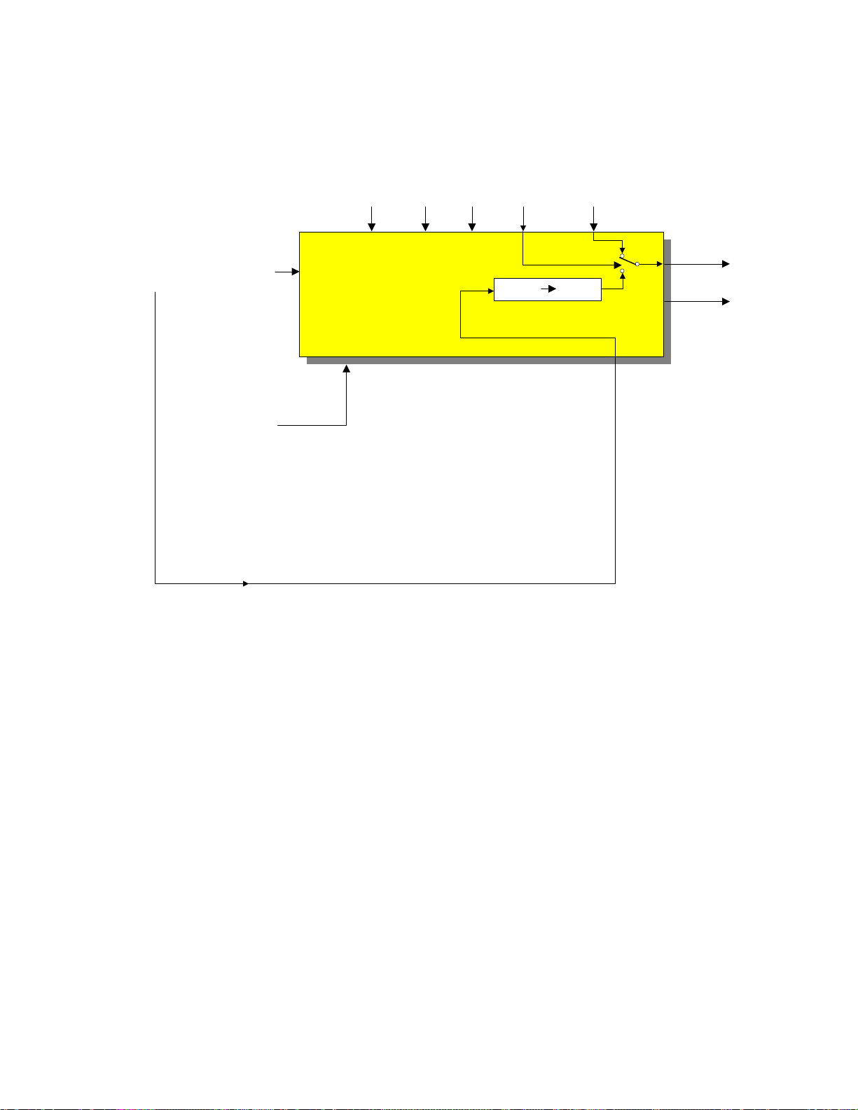
DP86 CHASSIS SYSTEM CONTROL & SIGNAL PROCESSING BLOCK
Clock/
Data/
Enable
PinP
YC
I2C +5V +9V +3.3V
3D Y/C Unit
and
PinP Unit
HC3152
VIDEO
YC
YUV
HV
6dB Amp
YUV
Clock/Data/
Enable
+9V
+5V
HC140538CP
HV
+5V
2H Sync
Selector
FC
UNIT
HC5125
Flex
Converter
2H YUV
H V
HV Blk
Clamp
YUV YIQ
+5V
YUV
Y
YUV
BA7657F
YUV Selector
Sync
Sep
V Sync
Sep.
PinP Y/C from Selector
IC
SIGNAL P.W.B.
HV
Sync
YUV Switch
PinP
Sync Det.
PinP V
To Microprocessor
Main
Sync Det.
Main Video/S-YC
from Selector IC
PAGE 01-07
Page 12

BLOCK DIAGRAM EXPLANATION
SYSTEM CONTROL AND SIGNAL PROCESSING
MAIN VIDEO FROM SELECTOR IC:
At the bottom left hand side is shown the Main Video
from Selector label. This is the NTSC video from the
selector IC. This is routed to two blocks.
3D Y/C:
The 3D Y/C separates luminance from the chroma. It
also add the 3D effect, (if the 3D Y/C is turned on
within the menu). Noise is canceled and the two separate components are output to the Video/Chroma Demodulator.
VIDEO/CHROMA DEMODULATOR:
This IC decodes the signal down to it’s Luminance and
Chroma. components and outputs it as 1HYIQ.
DM-1 I/F:
Noise cancellation and level shifting preparing the signal for the DM-1 module.
1HYIQ:
1HY = Standard NTSC format luminance. (Also
known as 480I).
I and Q = Standard NTSC format, demodulated
chroma components.
SYNC DET.:
Separates the Sync signal from the composite video signal.
SYNC DET.:
This block outputs composite sync to the PinP unit which
is used for timing for display. This is specifically related
to the Demodulator, D/As and Read/Write clock. The
Read/Write clock also is controlled by the frequency of
the Subcarrier also called fsc.
The Composite sync is also sent to the DM-1 on the line
labeled as 1H Composite Sync. The DM-1 uses this signal for OSD positioning, auto channel detection and AFC
loop activation.
TV uCOM MICROPROCESSOR:
This is the slave Microprocessor or Sub-Microprocessor.
This IC is in constant communications with the DM-1
module. The slave uP. Receives or outputs the following
signals;
HBLK: = Input; this is the Horizontal Blanking signal.
Used for Service OSD signal creation timing.
S.WIDE: = Output; when the customer watches regular
NTSC 4X3 aspect source, they have a choice of viewing
the signal in one of 4 ways.
Normal: This will display a standard 4X3 picture
with black panels on each side of the picture.
Fill: This will expand the picture to fill the screen.
The top and bottom will be cropped.
Full: This will expand the picture side ways and fill
the screen. However the picture will be non-linear.
Smooth Wide: This will keep the center of the picture linear and stretch the outside edges to fill the
screen.
With the four choices above, the DM-1 module controls
the signal for 3 of them; Normal, Fill and Full. However,
during Smooth Wide, the deflection circuit is switched to
perform the stretching of the sides. The slave Microprocessor outputs S.Wide during this time.
CUT OFF: = Output; labeled as V. Stop, during the Ser-
vice adjustments for Cut Off, (Screen Background controls), the vertical must be collapsed. This output causes
the B+ to the vertical output IC front end to be grounded
and grounds the vertical trigger pulse called V. Saw.
D. SIZE: = Output; labeled as Digicon Size, during
Smooth Wide mode, the Digital Convergence Unit, hear
after called DCU, must know that the set is in the distorted deflection mode. This signal tells the DCU just
that.
MAGIC SW: = Input; when the customer presses the
Magic Focus button on the control panel, the DCU notifies the slave micro. That it is busy performing Magic
Focus. The slave micro. Notifies the DM-1 module and
the DM-1 module ignores infrared pulses from the remote control.
CLOSED CAP. DATA: = Input; This input receives the
composite sync signal and decodes the Closed Caption
Data. (Data Slice line 21) and the communicates with the
DM-1 Module. The DM-1 Module actually introduces
the Closed Caption Characters into the Video stream.
F. PANEL: = Output, Dependant upon the customer’s
menu selection, will determine the IRE level of the side
panels when 4X3 Normal mode is used. By raising the
side panel IRE levels, the 4X3 picture won’t burn in the
CRT’s.
MAIN SYNC DET: = Input; this is used for detecting the
Closed Caption Data. This information is routed to the
DM-1 module for OSD generation. NOTE: the submicro. Doesn’t produce OSD characters for Closed Caption.
PinP SYNC DET: = Input; PinP tuner sync is routed to
the sub-micro. And is used during PinP tuner channel
Page 01-08
Page 13

BLOCK DIAGRAM EXPLANATION
SYSTEM CONTROL AND SIGNAL PROCESSING
selection to activate AFC.
MAIN SYNC DET. = Input; This input is used for Service OSD positioning and Auto Programming channel
detection.
PinP SYNC DET. = Input; This input is used for judgement of the Slave Microprocessor to determine the AFC
Loop activity of the PinP Tuner.
MUTE (Audio): = Output; during channel change, external video selection with no input, power up or power
off, and loss of Vertical Blanking, the audio and video
are muted.
V.MUTE (Video): = Output; during child lock, channel
change, or power on/off, the video is muted.
POWER: = Output; when the front power button or the
remote power button is pressed, the DM-1 module notifies the sub-micro. And the sub-micro. Outputs a power
on/off command to the relay driver Q-007. Outputs high
for ON and low for OFF.
OSD & OSD BLK: = Output, this is the on screen characters for the Service Menu only. OSD Blk is OSD
blanking. This cleans us the video where the OSD is to
be inserted.
HV BLK: = Input; this inputs are utilized by the Microprocessor for Service OSD positioning.
HV BLK PH: = Output; during Service Adjustment and
in the NTSC normal mode. This picture doesn’t fill the
screen. The areas on the side of the picture are called
Side Panels. This can be adjusted. The HV BLK PH,
controls the timing of the side panel OSD outputs.
SIDE PANEL APL FROM 2H VIDEO PWB: = Input;
the Microprocessor receives a pulse created within the
2H video PWB. This pulse represents the timing pulse
for the Side Panel OSD production.
Blocks continued;
OSD MIX: Only the Service menu OSD is output from
the Slave Microprocessor. The Digital convergence unit
puts out OSD characters as well. This characters product
the Service Grid and other text during Digital Convergence adjustments and/or Magic Focus. The two OSD
sources are received by the OSD Mix. This is comprised
of a quad Or Gate and outputs the signal to be superimposed upon the video signal path from the DM-1 Module.
PinP VIDEO FROM SELECTOR IC: The video from
the PinP tuner is routed to the PinP unit and the Sub Microprocessor for Closed Caption decoding.
Page 01-09
Page 14
DP86 CHASSIS SYSTEM CONTROL BLOCK
IR From
Control Panel
IR
I2C
YUV Switch
DAC
M62392
MTS
F. MONO
ANT
UV/IQ Sel
YUV Sel
SYNC On/Off
CUT OFF
31/33
To Deflection (DCU)
TV uCOM
Microprocessor
IR In
Dimmer
Key In
D. Size
Main Tuner Enable
PinP Tuner Enable
Sync Det
P.Blk.
Mute (Audio)
V.Mute (Video)
FH Det
FV Det
Power On/Off
OSD & OSD Blk
I2C
I2C
Cut Off
D. Size
31.57/33.75
To Deflection
Busy
Digital OSD
OSD RGB Ys
OSD
Select
IR
RGB Ys
OSD
Main Sync Det
PinP Sync Det
MEMORY
Main Video from Selector IC
CCD Video
Main
SIGNAL P.W.B.
HV BLK
YM
Busy
PAGE 01-10
Page 15

BLOCK DIAGRAM EXPLANATION 2H VIDEO
The 2H Video PWB is similar to the Rainforest circuits used in the past. The YUV/YIQ
(480P) and/or the Y-PR/PB (1080I) is routed
through another DM-1 Interface IC for noise
cancellation and level shifting and into the
Rainforest chip, IX01. Here the signal is prepared for the CRT’s. Pedestal level detection,
Chroma preparation, OSD RGB from either
the DCU or the Slave Microprocessor is input
here.
Remember that the OSD for Customer usage
such as the Channel numbers, clock, Main
Menu, etc.. is generated by the DM-1 Module.
Also, ABL controls the brightness and
Contrast; as well as the color level at this
chip.
The Velocity modulation control signal is
produced from the Rainforest IC. This signal
is a representative of the Peak White components of luminance and drives the Velocity
Modulation coils on each CRT.
Page 01-11
Page 16
2H PWB BLOCK DP86 CHASSIS
2H VIDEO P.W.B.
OSD RGBYSI2C YM ABL
YUV/YIQ/
Y PB PR
+9V
Clamp
HV Blk
RGB PROCESSOR
TA1276AN
Clamp
H/V Blk.
YUV RGB
YUV
YIQ
YPBPR
RGB
VM
PAGE 01-12
Page 17

BLOCK DIAGRAM EXPLANATION DEFLECTION BLOCK
The 61HDX98B deflection circuit differs from conventional Hitachi product. It utilizes in a sense, two
horizontal output circuits. One for Deflection and on
for High Voltage. The notations around the Block diagram will be described in a counter clock wise fashion
as best a possible.
CUT OFF:
Cut of collapses the Vertical circuit during I2C Bus
alignments, during CRT Set Up.
I2C:
Communication from the Sub Microprocessor I001
during sweep variations due to Standard/NTSC 480P
mode and 1080I High Definition mode.
ABL:
ABL voltage is generated by monitoring the current
through the flyback transformer. This voltage will
fluctuate down when the scene is bright and up when
the scene is dark. The ABL voltage will manipulate
the screen brightness and contrast to prevent blooming
under these conditions.
HV SYNC:
The composite sync is routed into the Sync processor
which determines the sweep condition for the signal
being provided.
H and V BLK:
Horizontal and Vertical Blanking is developed within
the Deflection circuit. The Horizontal Blanking pulse
operates around 13V P/P and is produced by taking a
sample pulse from the Deflection transformer T752.
The Vertical Blanking pulse is generated from the
Vertical output IC, I601 pin 7. This pulse normally
operates at 23V P/P.
IR:
The Infrared Pulses coming from the remote control
are routed through the Deflection PWB to the Digital
Convergence Unit. During DCAM (Digital Convergence Adjustment Mode), the Remote Control provides manipulation pulses for the DCU.
DIG RGB BUSY:
This indicates Digital RGB and BUSY.
Digital RGB represents the on screen characters produced by the DCU for generating the Digital Convergence adjustment grid and text produced during certain conditions such as Magic Focus, Sensor Initialization, Data Storage, etc…
Busy notifies the sub Microprocessor I901 which in
turn notifies the DM-1 module that the DCU has entered the DCAM. During this time, the DM-1 module
ignores the remote control commands.
MAGIC SW:
When the customer presses the Magic Focus button on
the front of the set, it produces a command for the
DCU to begin the Magic Focus process.
D SIZE:
Digital Size is a control signal for raster enlargement
when MAGIC FOCUS is operated. Raster enlargement is required for the MAGIC FOCUS PATTERN
to hit the photo sensors.
This signal is output from DCU and input to the Sub
Microprocessor I901. The Sub Microprocessor controls the I702 on the DEF.SUB PWB) for enlarging
raster size.
In case of AP-85, this control signal is called "A.
SIZE". It's the same function between DIG.SIZE and
A.SIZE.
S WIDE:
Smooth Wide is a condition entered through the Menu
by the customer while watching an NTSC 4X3 aspect
video source and the customer wants to fill the screen.
TO CONVERGENCE YOKES:
The DCU provides compensation signal for deflection
abnormalities to the convergence output IC. The Convergence output IC in turn, amplify the signals and
rout them to the convergence yokes.
+26V, 26VP and RETRACE PULSE:
The positive 26V and the negative 26V is routed to the
Deflection transformer I752. They enter the transformer as a pure DC voltage. A 15V P/P horizontal
pulse is added to the DC voltage and leaves as +26VP
and –26VP. From here these voltages are routed to the
Convergence output section and they are rectified.
They become +33V and -33V respectively. This process prevents the need for another power supply.
+B 130V:
The Deflection transformer receives the 130V V1 DC
source.
DF OUT:
Generated from the I702 on the Sub Deflection PWB
and the Horizontal Blanking pulses, a Dynamic Focus
waveform is created. This is a parabolic waveform that
Page 01-13
Page 18

BLOCK DIAGRAM EXPLANATION DEFLECTION BLOCK
is superimposed upon the static focus voltage to compensate for beam shape abnormalities which occur on
the outside edges of the screen because the beam has
to travel further to those locations.
HV PARABOLA:
Described above.
SCREEN 700V: 700V Supplied to the screen grids on
the CRT’s.
FOCUS 9KV:
Focus voltage supplied to the CRT’s.
32Kv HV:
32,000 volts DC supplied to the CRT’s anodes.
TO DEFLECTION YOKES:
Horizontal and Vertical deflection wave forms driving
the deflection yokes.
INTERNAL BLOCKS DESCRIPTION
HV CONTROL:
The uPc1344C IC generates the horizontal drive signal
utilized by the High Voltage circuit. The HV control
IC receives it’s locking pulse from the Deflection circuit. A feed back voltage is sampled from the High
Voltage Regulation Detector circuit and compared
with a reference voltage to maintain an accurate 32KV
on the CRT’s.
VERTICAL OUTPUT:
The vertical output utilized in the 61HDX98B operates
differently from previous chassis. This circuit utilizes
a +13V and a –13V to generate the waveform to drive
the vertical deflection yokes. A pump up circuit is utilized to product the retrace pulse for the vertical deflection yoke. It’s at this time when a higher pulse is
needed because the beam has to travel from the bottom
of the screen to the top very rapidly. The vertical output IC receives it’s trigger pulse from the ramp generator.
SYNC PROCESSOR:
The Sync Processor located in I702 on the Sub Deflection PWB, detects the horizontal sync rate for the displayed signal, either 480P or 1080I.
VERTICAL RAMP GENERATOR:
I702 on the Sub Deflection PWB generates the Vertical Saw signal. This signal is controlled by several
factors. The Sync Processor detection and I2C data
communication.
DIST CONTROL:
Distortion control is another signal produce by I702
and sent to the Side Pin cushion circuit. These compensation parabolic wave forms are combined with the
horizontal circuit to compensate for Side pincushion
errors.
H-SIZE SIDE-PIN CONTROL:
This circuit generates the Side Pincushion Distortion
compensation pulse which is impressed onto a coil
located in the output side of the Deflection Output section and compensates for Pin Cushion distortion.
HORZ. DRIVE and HORZ. OUT:
This circuit comprises the Drive and Output for the
Deflection output circuit.
S-CORRECT (SMOOTH MODE):
During Smooth mode, the deflection circuit is manipulated so that the outside 1/3 of the picture is stretched
to fill the screen. The center 2/3 of the picture is left
undistorted. When an S Wide signal is received, a capacitor is switched off on the output side of the Deflection output circuit.
PHOTO SENSOR:
There are 8 sensors located on the internal outside
edges of the cabinet. These Photo Cells receive the
light patterns being generated during MAGIC FOCUS
or SENSOR INITIALIZATION and deliver this voltage to the Sensor Distribution circuit.
SENSOR DISTRIBUTION:
This represents the amplifiers that receive the Photo
receivers (Photo Cells) inputs during Magic Focus operation.
DIGITAL CONV. UNIT:
This is the Digital Convergence Unit. This is a nonrepairable unit. It contains the distortion compensation
wave form generation circuits, RAM, ROM and D/A’s
for the convergence circuit.
SERVICE SWITCH:
When the set needs a convergence alignment, the Ser-
Page 01-14
Page 19

BLOCK DIAGRAM EXPLANATION DEFLECTION BLOCK
vice Switch is pressed. This switch is located on the
deflection PWB. By removing the front speaker grill,
the Service Technician has access to this switch.
CONV. OUT:
The Convergence output block represents the two (2)
Convergence output IC’s. These two IC’s contain the
amplifiers for the Red, Green and Blue convergence
outputs.
HDT T752:
Represents the Deflection output transformer. By
separating the Deflection circuit from the High Voltage, any distortions that would be generated by fluctuations within the High Voltage won’t be visible
within deflection.
DYNAMIC FOCUS OUT:
This circuit amplifies the parabolic signals provided
by the Deflection circuit and I702 on the Sub Deflection PWB and impresses these wave forms onto the
static DC voltage use for focus. This keeps the beam
as sharp or focused as possible in the corners of the
screen.
HIGH VOLTAGE REGULATION DETECTOR:
This circuit monitors a feed back voltage produced
from the High Voltage Flyback transformer and routes
an output signal to two circuits.
1.) A sample voltage is sent to the Horizontal Driver
IC for regulation of the High Voltage and;
2.) If the High Voltage climbs too high, a shut down
signal is produced to shut down the power supply until
a repair can be made.
FOCUS PACK:
The focus pack receives the Focus voltage and the
High Voltage and distributes them to the CRT’s.
FBT TH01:
Is the main Flyback Transformer producing High
Voltage.
Page 01-15
Page 20

H Blk
HV Pulse Shape
HD74LS221P
HV Control
(uPC1394C)
DP86 DEFLECTION BLOCK DIAGRAM
To Deflection YokesTo Deflection Yokes
HV DRIVE
HV OUT
(IMB12-140)
ABL
32Kv
HV
High Voltage
Transformer
ABL
Cut
Off
I2C
HV Sync
V Blk
IR
Dig RGB
Busy
HV Blk
PAGE 01-15
C
2
I
SYNC.
PROCESSOR
H Blk
PHOTO
SENSOR
SENSOR
DISTRIBUTION
From uP
Magic SW
uPC1885
H Drive
/ 8
VERTICAL
OUT
LA7648
VERTICAL
RAMP
GEN.
Busy
Dig RGB
8
/
DC couple
/
3
S Corrected
V-SAW
CONTROL
H Blk
IR
DIGITAL
CONV.
UNIT
DIST.
HV Blk
6
/
V Parabola
Saw
HORZ.
DRIVE
2SC3116
SERVICE
SWITCH
Size Regulation
+
Diode
Modulator
Control
H-SIZE
SIDE-PIN
CONTROL
HORZ.
OUT
2SC5413
REGULATION
Vcp
VOLTAGE
DETECTOR
Parabola
1100V
+26V,
-26V
HV
+
H Blk
FBT
THO1HIGH
FOCUS
PACK
Focus
12Kv
DYNAMIC
FOCUS OUT
2SC4686X3
Deflection Transformer
HDT
T752
Retrace Pulse
+
+26P,
-26P
CONV.
OUT
3
/
/
3
DF
Out
+B (130V)
34v, -34v
6
/
To Convergence
Yokes
Focus
(9KV)
Screen
(700V)
D Size
31.5/33.75
Page 21

220V
9V
DP86 CRT PWB BLOCK DIAGRAM
Beam Shape, Beam Alignment,
Focus, VM Coil,
CPT P.W.B. (R)
VIDEO OUTPUT
R
AMP
Deflection and Convergence Yokes
R
220V
9V
220V
9V
220V
26V
CPT P.W.B. (G)
VIDEO OUTPUT
G
CPT P.W.B. (B)
VIDEO OUTPUT
B
VM OUT P.W.B.
G
AMP
B
AMP
VM OUT
PAGE 01-16
RGB
VM
SCREEN
FOCUS CONV.
Def.
Yokes
30KV
HV
Page 22

AUDIO OUTPUT SECTION DP86 CHASSIS
+9V
HiFi Out L/R
Transmitter Out
FL/FR
RL/RR
PinP L/R
SELECTOR
MC14052
PinP L/R
FR
to Spk
FL
SL/RS
FL/R
From
Audio/Video
Selector IC
I2C
+9V
CONTROL
TDA9860
Graphic Equalizer
Perfect
Volume
L/R
Pro Logic
Decoder
Passive
Decoder
H/H-L/R
L/R/C/LFE/LS/RS
L/R/C
R
H/H-L/R
H/H-LS/
RS
L/R
L R
Front
Audio
FL/R
Amp
TA5200AH
28V
Center
Audio Amp
21V
Sub Woofer
Rear
R
Audio
L
Amp
TA5200AH
Audio Out PWB
C
SL/RS
28V
I2C
CONTROL
C
Clock
Data
+9V
SL/RS
I2C
CONTROL
Surround PWB
+9V
Clock
Data
L/R/C/LFE/LS/RS
+9V
I2C
TDA9860
Graphic Equalizer
TDA9860
L/R/C/LFE/LS/RS
PinP L/R
C/LFE
H/MS
H/H-LS/RS
PinP L/R
From
Selector IC
+9V
Ext. Decoder In
PAGE 01-17
Page 23

REAR SPEAKER
8 ONLY
+
+
DP86 REAR PANEL (60SDX88B)
ANT A
PAGE 01-18
R L
-
EXT. DECODER INPUT
LS C
RS LFE R
R L
AUDIO TO HI-FI
R L
R L
WIRELESS OUT
-
L
SUB
WOOFER
To
Converter
ANT B
S-
VIDEOS-VIDEO
VIDEO
(MONO)
AUDIO AUDIO AUDIO
INPUT 1 INPUT 2
VIDEO VIDEO
(MONO)
L
R
COMPONENT VIDEO
(MONO)
L
R
INPUT 3
Y PBC
VIDEO
(MONO)
L
R
AUDIO
MONITOR OUT
PRC
B
R
L
S-
VIDEO
R
Page 24

A 16X9 ASPECT IMAGE DISPLAYED ON A 4X3 ASPECT SCREEN
UNDERSTANDING TOP AND BOTTOM
PANELS:
When a 16X9 Aspect (1.7777 to 1) images is
shown on the DP-86 set with a 4X3 Aspect
(1.3333 to 1), ordinarily there would be top
and bottom panels that are black. If the set
were to continuously operate in this fashion,
it’s possible that the area of the screen that
has images would age and the area that doesn’t display an image, i.e. the top and bottom
panels, wouldn’t.
In other words, the image may burn onto the
screen. To prevent this from happening, the
top and bottom panels are replaced with On
Screen Display that are gray in nature.
(Above black IRE level.) This allows the top
and bottom to age at the same rate as the used
portion of the CRT surface.
UNDERSTANDING LETTERBOX:
Letter box is commonly used with DVD or
when the broadcast wants to display the complete panoramic view of the theater. This
means that the image which is something
other that 4X3 is created in a 4X3 environment. Of course, the same situation as described above exist, except this one has an
exception. The exception is this, the area of
the top and bottom panels is active video.
Even though it’s black, the TV doesn’t know
if it’s top and bottom panels or video. So the
top and bottom panels in this situation are
black.
RULE OF THUMB:
If the top and bottom panels are BLACK,
then the screen can not be manipulated using
Screen Format in the menu.
This will help when confronting consumers
that question why they can’t manipulate the
screen in this condition.
USING A SET TOP BOX:
When using a Set Top Box to receive ATSC
signals and imputing these signals into the
Component input, many times the broadcasters are converting NTSC signals into ATSC
for broadcast. This causes a similar problem.
In other words, the 4X3 NTSC original signal
is modified to fit into the 16X9 ATSC environment and again the Top and Bottom Panels will be BLACK. Nothing can be done using Screen Manipulation to elevate this problem.
Page 01-19
Page 25

DP-86 CHASSIS DISPLAYING A (16x9) IMAGE ON (4X3) DISPLAY
Top and Bottom Pannels are OSD Generated
Top Pannel
Slightly
above
black
to avoid
16X9
burning
an image
Bottom Pannel
PAGE 01-20
Page 26

DP86 SUB POWER SUPPLY SHUTDOWN BLOCK
(SIGNAL) LOW VOLTAGE
I901
ShutDown Pin (7)
I905
on Power Supply
7 3 2
Photocoupler
Driver &
Output IC
Shut Down SCR
+5V Too Hi Det.
+9V Too Hi Det.
TV5V Short Det.
TV9V Short Det.
+12VS Too Hi Det.
PAGE 02-01
Page 27

I901
ShutDown Pin (7)
on Power Supply
Driver &
Output IC
5
R908
D905
DP86 SUB POWER SUPPLY SHUTDOWN DIAGRAM
(SIGNAL) LOW VOLTAGE
DIGITAL & SIGNAL
POWER SUPPLY SHUT-DOWN
Active High
7 3 2
I905
Photocoupler
D908
Run B+
R919
Red LED
Shut Down
Identification
D959
DIGITAL & SIGNAL
POWER SUPPLY SHUT-DOWN
Active Low
Q913
ShutDown
S.C.R.
TV5V Short Det.
R907
D964
1/2 AC In
Start Up B+
No Start Up B+ = Off
Normal = Glowing
Blinks during Shutdown because
of the internal current draw.
15.1V ~ 22.5V pin 5 I901
TV5V Too Hi Det.
TV9V Too Hi Det.
+12VS Too Hi Det.
+5V
+9V
+12VS
D974
D975
D936
Q917
STBY +12V
Off
Off
Q914
D972
D925
TV9V Short Det.
On
R9A
0
On
C
E
Off
E C
B
D958
PQS1
B
TV5V
TV9V
Vcc
Q916
Power5
On
+12VS is the same as A12V or SB12V
PAGE 02-02
Page 28

DP86 CHASSIS L.E.D. (VISUAL TROUBLE DETECTION) DIODES
(SUB POWER PWB) SIGNAL POWER SUPPLY 5 GREEN L.E.D.s and 1 RED L.E.D.
(6 Total L.E.Ds. for visual trouble sensing observation)
D908 is a RED L.E.D.
Off = No I901 B+
On (Mid) = I901 B+
On (Bright) = Shutdown
PAGE 02-03
D908
R919
Audio
F/R 28V
R927
D919
Center 21V
Osc B+
1.9V
Audio
R928
D920
ALL GREEN L.E.D.s
Start Up or Run
24.2V
Driver/Output IC
100% Dead Time &
7
IC B+ Detection
TV 9V
R945
D930
5
I901
TV 5V
R9E3
D971
R916
+12VS
D928
24.2V
1.9V
R956
4
3
Vcc
I905
I905 Shutdown
Photocoupler
5 Shut Down
Inputs
1
2
Q913
Shutdown
SCR
Page 29

AC Plug
AC Input
DP86 SUB POWER SUPPLY DISTRIBUTION DIAGRAM
(SIGNAL) LOW VOLTAGE
Live Cold
Protector
E994 : 7K
Rectifier
+28V : D911
D919 : F28
FT / REAR +28V
Audio
+28V
PAGE 02-04
FUSE
F901
Noise Filter
L901, 2, 3
Rectifier
D901
Protector
E992: 7K
Switching
Control
I901
D908:
Protect Red LED
To
Deflection
Power Supply
Protection
Block
Switching
Transformer
T901
Feedback
I904
Protect
I905
AC Clock
I906
RELAY
S901
Relay
S902
Relay
S903
DP86
Only
AC Clock
60Hz
Protector
E995 : 7K
Protector
E996 : 5K
Voltage
Control
24, 5V
Q915
Rectifier
+21V : D912
Rectifier
+35V : D918
Rectifier
+24V, 5:D914
TV ON/OFF
Switch
Q914, Q918
TV Main ON/OFF
ON = LO
OFF = Hi
D920 : C21
A12V
Regulator
+12 : I907
Regulator
TV9V : I908
Regulator
TV5V : I914
Protector
SCR: Q913
= RED OR GREEN L.E.D.
STAND BY +12V
D928 : +12V
D930 : TV9V
D971 : TV5V
Short Circuit
Detector
CENTER +21V
D
D
"D"
D925:
<4V
D972:
<4V
Audio
+21V
33VS :
D936 : >14.7V
ZD
D975 : >10.8V
ZD
D974 : >6.7V
ZD
Over
Voltage
Detector
+33V
+12VS
+9V
+5V
Page 30

DP86 DEFLECTION POWER SUPPLY SHUTDOWN
BLOCK DIAGRAM
IP01
ShutDown Pin (7)
on Power Supply
Driver &
Output IC
220V Short Det.
Heater
Short Det.
13V
Short Det.
28V Short Det.
Deflection B+ (130V)
Excessive Current Det.
IP06
Photocoupler
QP06
QP05
ShutDown
S.C.R.
DP25
Heater Too
High Det.
-M13V
Loss Det.
-M28V
Loss Det
Deflection B+ (130V)
Excessive Voltage Det.
DP23
DP34
X-RAY
PROTECT
Flyback
Excessive
Current Det.
Heater Loss
Det.
Excessive
High Voltage
Det.
Deflection
Transformer
Failure Det.
Side Pin
Failure Low
Det.
Q754
Side Pin
Failure High
Det.
High Voltage
Stability Too
High Det.
PAGE 02-05
Page 31

DP86 DEFLECTION POWER SUPPLY SHUTDOWN DIAGRAM
TP91
DP11
13
CP16
IP01
ShutDown Pin (7)
on Power Supply
Driver &
Output IC
200V Short Det.
DP37
220V
Heater
DP36
DP35 ?
QP04
RP31
0.47
DP17
DP19
IP06
Photocoupler
Excessive High
Voltage Det.
DP35 May Not Be in Set.
Deflection B+ (130V)
Excessive Current Det.
DP18
DP23
QP05
ShutDown
S.C.R.
DP25
DP34
Deflection B+ 130V
Deflection B+ (130V)
Excessive Voltage Det.
Deflection Flyback
Excessive Current Det.
Flyback
TH01
9
QH03
10
DH24
5
DH31
QH07
DH30
RH23
1.2
Heater
DH25
DH26
DH27
Doesn't
go to
CRT's
Heater Loss Det.
DP30
13V
DP31
28V
DP27
DP26
RP45 RP44
-M28V
-28V Loss Det. -13V Loss Det.
+28V
Deflection B+ 130V V1
DP29
DP28
RP41 RP40
-M13V
Q777
QP06
13V Short Det.
28V Short Det.
+13V
6
1
DP33
DP32
Heater from Def. Power Supply. Goes
to CRT's
Heater To High Det.
7
8
T752
H.Blk
X-RAY
PROTECT
RP42
D759
C769
QH06
High Voltage Stability Too
D753
D757
Deflection Transformer
D754
Side Pin Failure High
Q754
D756
Inoperative Det.
High Det.
Det.
D760
Side Pin
Failure
Low Det.
PAGE 02-06
Page 32

13V
DP86 CHASSIS L.E.D. (VISUAL TROUBLE DETECTION) DIODES
DEFLECTION PWB 5 GREEN L.E.D.s and 1 RED L.E.D.
(6 Total L.E.Ds. for visual trouble sensing observation)
130V
+28V
Deflection B+
RP39
-M28V-M13V
DP06 is a RED L.E.D.
Off = No IP01 B+
On (Mid) = IP01 B+
On (Bright) = Shutdown
PAGE 02-07
RP23
DP15
DP06
Osc B+
1.9V
RP37
ALL GREEN L.E.D.s
Start Up or Run
24.2V
5
IP01
Driver/Output IC
100% Dead Time &
7
IC B+ Detection
RP38
RP60
24.2V
1.9V
RP26
DP16DP22DP20
4
3
Vcc
IP06
IP06 Shutdown
Photocoupler
16 Shut Down
Inputs
RP46
DP21
1
2
QP05
Shutdown
SCR
RP17
Page 33

DP86 DEFLECTION POWER SUPPLY DISTRIBUTION DIAGRAM
Power Supply
Block
Protector
EP91: 4K
Switching
Control
IP01
PAGE 02-08
DP06:
Protect
Red LED
Live Cold
Switching
Transformer
TP91
Feedback
IP05
Protect
IP06
Protector
EP92: 4K
Protector
EP93: 5K
Protector
EP94: 7K
Protector
EP95: 7K
Protector
EP96: 7K
Protector
EP97: 7K
Voltage Control
+130V: IP04
Rectifier
+220V:DP07
Rectifier
+7V:DP08
Rectifier
+15V:DP09
Rectifier
+15V:DP10
Rectifier
+28V:DP12
Rectifier
-28V:DP13
Rectifier
+130V:DP11
Regulator
+6.3V: IP02
Regulator
+13V: IP03
Regulator
-13V: QP01
Protector
EP96: 7K
Protector
SCR: QP05
DP36, DP37:<4V
D
DP35: <4V DP32: >7.4V
D
DP15: +13V DP30: <5V
D
DP16: M-13V DP28: > -13V
D
DP20: +28V DP31: <5V
D
DP21: -28V
DP22: +130V QP04: >1.4V
Protect In
DP25: >-24V
D
D
Short
Circuit
Detector
Over
Voltage
Detector
Power
On/Off
ZD
DP28: >20V
ZD
DP26:
>32V
ZD
DP18:
>166V
ZD
HVcc
Switch
QP08
Video +220V
Heater
+6.3V
Vert/HVcc:
+13V
Vert:
-13V
Conver:
+28V
Conver:
-28V
Deflection
+130V
HVcc
+12V
DP-85 Deflection
Circuit Protection
Page 34

DP86 SERIES CHASSIS HORIZONTAL DRIVE
CIRCUIT
Q701
PDD1
7
9
To I001 OSD
Position
To PinP
Unit
I702
H Out
18 16
29
FBP In
17
26
PSD2
6
H.Blk.
HVCC
Switched AVCC
Osc.
H. Sync In
Q755
C771
To Convergence Circuit
To Sweep Loss Det. Circuit
IH01
A1
1
Q751
C770
Q2
28V
12
3
1
T751
10
6
4
130V V1
IH02
Osc
Q777
Drive
H. Def. Yoke R
H. Def. Yoke G
H. Def. Yoke B
T752
1
6
QH08 QH01
7
8
11
12
9
10
Def.
H Pulse
+28V
+28P
M28V
M28P
QH09
7
To Side Pin Circuit
To Dynamic Focus
To Deflection Loss
To X-Ray Protect
130V V2
TH01
9
High
Voltage
10
PAGE 03-01
12
13
Clamp
QH10
14
E
r
r
o
r
1
Ref. V.
FBP In
QH05
QH04
HV Sample
12
QH06
HV Sample too High
X-Ray Protect
Page 35

4V
Avx 4 In
S-4 In
DP-86 SERIES CHASSIS VIDEO SIGNAL PATH (Main & Terminal)
Front Control PWB
Signal PWB 1 of 2
U002
Main Tuner
S Det.
Aux Input 4
Q036
18
Terminal PWB
PFT
V4V
S-Y4
S-C4
9
5
3
PST1
8
Lum/Audio Selector IC
I301
19
21
23
TV1V
Main
Video
5
NTSC
VOut2
YIn2
CIn2
Vout1
Yin1
PinP Yout2
34
PinP C Cout2
32
36
38
46
48
4
V In
1
Y Out
C Out
330
C309
Q312 Q313
Line
Comb
Filter
Q303
2
Q306
Q305
Monitor Out
PinP VY
PinP C
PST2
1
3
U004
18
16
PinP
Unit
And
3DYC
PinP TUNER (Mono)
V1
Aux Inputs
S-1 In
V2
S-2 In
V3
PZC
QX23
1
R
To CRT PWB
QX28
3
PAGE 04-01
G
QX33
5
B
U003
Always PinP
IX01
43
Rain
forest
42
41
2H Video PWB
23
53
52
51
S Det.
S Det.
Y2 In
QX10
U/Q In
QX08
V/I In
QX09
Q039
3
PSZ2
16
18
20
Q061
Q062
Q063
TV2V
S-Y1
S-C1
S-Y2
S-C2
U006
FLEX
Conv.
2
7
9
11
13
15
17
50
PFC1PFC2
113
314
215
PinP
Video
Q042
Yout1
Cout1
1HY
Q043
1HV
1HU
44
42
Component
I013
21
15
19
Y/S Monitor Out
Inputs
U
V
Y
1
1
7
2
1
5
11
2
1
3
9
2
PST3
11
13
9
Q048
Q019
Q046
Q301
Q302
SIGNAL PWB
Q049
V
U
Q051
Q054
Q050
SIGNAL PWB 2 of 2
Yout1
Cout1
2 of 2
Q067
Q052
Q053
11
13
18
20
12
10
8
Yout
V(R-Y)
U(B-Y)
Page 36

DP86 CHASSIS A.B.L. CIRCUIT DIAGRAM
See uP
Data
Signal
Path
PSZ2
RX78
RX79
QX14
RX80
9V
DX02
RX82
ABL
9
DX01
CX21
CX20
RX81
CX24
CX39
PSZ1
QX54
16
SDA2
SCL2
17 28
RH22
High Voltage B+ 130V V2
QH03
See XRay Protect
RH23
CH18
RH24
To QH01
Collector of Horz.
Output Transistor
45
27
SDA2
IX01
Rainforest
IC
SCL2
TH01
B+
C
ABL
3
2H Video
PWB
or
Signal Sub
PWB
To Anodes
To
Focus
RH67
LH03
PAGE 04-02
Signal
PWB
PSD2
1
ABL Pull-Up Resistors
Deflection PWB
Deflection B+ 130V V1
[ Current Path ]
13V
RH59RH58
Clamp
As Brightness goes Up, ABL Voltage goes Down. (Inverse Proportional)
CH25
RH56
DH33
CH31
Page 37

DP86 SWEEP & AC LOSS DETECTION CIRCUIT
12V
Vertical
Blanking
From
Pin 9 I601
V. Blk.
24V P/P
Horizontal
Blanking
From
Q755 Emitter
CN04
H. Blk.
11.6V P/P
SPOT
From Pin 9
of Micro I001
Cut Off
Vertical
Output IC
I601
Invert Input
Non Invert
Input
5V
R604
R605
CN01
CN03
6
4
RN02
RN11
RN12
PSD
2
2
3
RN03
QN01
RN01
12V
RN09
QN05
Prevents CRT Burn
DN09
Q610
Vert SAW
R602
Q601
Q602
Stops Vertical Drive
during Cut Off
adjustment, I2C
DN01
RN10
DN04
DN05
RN04
CN02
RN06
QN03
DN06
RN13
Spot Inhibit
QN07
QN06
8.57V
DN02
DN03
RN07
0V
RN08
DN11
DN10
RN16
RN15
CN05
DN07
9.72V
RN17
QN02
A12V
8.57V
CN06
RN05
QN04
DN12
DN16
DN14
DH41
Horz. 13V Loss/
Start Up Horizontal
Drive Killer
QH02
14
1
13 Error Out
12
Heater
Voltage
from
TH01
7
Stops High Voltage
Drive Signals From
being produced
during 13V start up
RN14
DN08
RN17
RH30
High Voltage
Driver IC
IH02
Reference
Feed Back
Error In
Drive
From I906 Pin 3
AC Photo Coupler
10V P/
P
ACK 5V
RN18
PAGE 04-03
Page 38

60SDX88B (DP-86 CHASSIS) AUDIO SIGNAL PATH
(Main, Terminal & Audio Output)
4L
Avx 4 In
4R
Page 05-01
Center L Spk
Center R Spk
Aux Input 4
Microprocessor
Front Left Spk
Front Right Spk
Front Control PWB
U002
Main Tuner
I001
Signal PWB 1 of 2
Left Rear Spk Jack
Right Rear Spk Jack
Surround PWB
2 of 2
PL
2
PR
2
PCL
2
PCR
2
27
1 of 2
26
SCL1
47
SDA1
43
PSP2
5
7
Center Left Out
Center Right Out
5
6
PST1
5
4
PST3
Terminal PWB
PFV
Terminal PWB
8
7
TV 1 Left
TV 1 Right
1L
Aux Inputs
1R
2L
2R
3L
3R
Rear Left
Rear Right
FT/Audio Output IC
12
I401
FL
7
FR
11
2
4
SCL1
SDA1
AVX 1
AVX 2
AVX 3
Front Left
Front Right
20
22
Lum/Audio
Selector IC
4
Tuner
Audio
6
27
26
8
10
14
16
51
49
Rear Output IC
12
I403
7
Q403
12
7
I402
Center Audio
Output IC
I301
Main Audio
PinP
Audio
Out
PinP
Audio
In
2
4
Left Monitor Out
Right Monitor Out
Signal PWB 2 of 2
Left Total
Right Total
PinP Left
PinP Right
Left Select
Right Select
PSU1
1
2
9
10
45
43
35
33
PST1
10
11
L
13
R
14
1
1
2 of 2
Mono PinP
PinP Tuner
20
U003
(See Surround Audio Signal Path)
3
PAS2
Rear Left
Rear Right
F L Out
Main Audio
D414
Front Speaker Off
D415
Mute
2
F R Out
Center
4
Audio Output PWB
8
9
1
2
4
(See Surround Audio Signal Path)
Page 39

60SDX88B DP86 CHASSIS SURROUND AUDIO SIGNAL PATH
PAS2
1 of 2
RL
8
RR
9
S Out
S In
9 8
3
8
IS02
Center
PSU1
1
2
9
10
L
1
R
Perfect
10
Volume
PinP Left
PinP Right
IS06
Passive
Decoder
IS08
28
30
LFE
LFE Out
See Audio Signal Path (Main & Terminal)
PAS2
2 of 2
Center Out
4
15
1
PinP
Audio
Control
C Out
C In
(Rear)
13
R Mix Out (Off/Matrix/Hall)
15
L Mix Out (Off/Matrix/Hall)
16
(Rear)
10
L inR in
IS04
2
Buffer
6
External Decoder In
32
1
3
20
13
5
24
23
R Out
L/R
Ext LFE In
Ext C In
Center
PinP Audio L&R to
Transmitter
Out circuit
LFE
Rear Left to Transmitter Out Circuit HiFi (R) L
Rear Right to Transmitter Out Circuit HiFi (R) R
L-R Amp
Rear
6
IS07
IS05
34
Pro
Logic
Decoder
L
1
7
9
R
10
L Out
R Out
35
Center
Out
37
36
3
5
28 30
IS01
Audio
H/MRH/ML
Ext LS In
Ext RS In
Ft L Out
24
Ft R Out
9
Control
Ext FL In
Ext FR In
Ext LFE In
Ext C In
1
32
CSG1 CSG2
23
10
18
15
Front L
Front R
7
Ft L In
Ft R In
H/MRS
S M/H R In
H/MLS
Rear
Rear Audio Control
IS03
30
RL Out
Rear
RR Out
28
24
RL RR
23
1
Rear R In
32
9 10
See
Graphic
EQ
Circuit
IG01~15
RR Out
18
15
9
10
RR In
IS10
1
3
Sub Woofer Buffer
5
7
PAGE 05-02
1
2
F L Out
F R Out
Front Right and Left to
Transmitter Out circuit
Page 40

60SDX88B DP86 FRONT AUDIO RIGHT & LEFT
For continuation of Front Left and Right Audio signal flow, see 60SDX88B DP-86 Chassis
Surround Audio Signal Path Diagram (Surround and Main/Terminal)
FRONT
AUDIO CONTROL IC
IS01
FR In
FL Out
FR Out
10
23FL In
24
9
GRAPHIC EQUALIZER CIRCUIT
-
Left
Front
Vcc
Right
Front
FL In
FR In
GEQ Clock
17 16
IG02
Front EQ
IN1L
2
IN2L
3
Left EQ
15
5V
Right EQ
IN2R
26
27
IN1R
2
3
5
6
Data
4
5
6
7
8
9
10
19
20
21
22
23
24
25
+
IG01
Buffer
+
-
10KHz
4.5KHz
2KHz
1KHz
400Hz
150Hz
60Hz
60Hz
150Hz
400Hz
1KHz
2KHz
4.5KHz
10KHz
1
FL GEQ
Front Graphic Equalizer
FR GEQ
7
Determines the Frequency Characteristics
controled by Customers OSD Menu.
"See Microprocessor Data Communication
Path" Diagram for more details.
IG09
IG08
IG07
IG06
IG05
IG04
IG03
PAGE 05-03
Page 41

For continuation of Front Left and Right Audio signal flow, see 60SDX88B DP-86 Chassis
Surround Audio Signal Path Diagram (Surround and Main/Terminal)
CENTER/LFE/PinP
AUDIO CONTROL IC
IS02
23Center In
Center
Out
24
60SDX88B DP86 CENTER
GRAPHIC EQUALIZER CIRCUIT
-
C Out
GEQ Clock
17 16
2
3
5
6
Data
+
IG10
Buffer
+
-
1
C GEQ
Center Graphic Equalizer
7
Determines the Frequency Characteristics
controled by Customers OSD Menu.
"See Microprocessor Data Communication
Path" Diagram for more details.
Vcc
Center EQ
IN1L
2
IN2L
3
15
5V
IN2R
26
27
IN1R
IG11
10
19
20
21
22
23
24
25
4
5
6
7
8
9
1
7
1
7
1
7
1
10KHz
4.5KHz
2KHz
1KHz
400Hz
150Hz
60Hz
IG15
IG14
IG13
IG12
PAGE 05-04
Page 42

DP86 Series Chassis AUDIO and VIDEO MUTE Circuit
Also see Mute Circuit Diagram (Surround and Audio Output PWB)
I001
V MUTE
Micro
Processor
16
A5V
A5V
RO21
RO22
D031
A12V
ROA6
ROA7
D032
D030
R0A4
R155
R0A5
Q033
PDS2
2
R0A2
R0A3
D034
C048
R0A8
Horizontal & Vertical
Sweep Loss Det.
AC Loss Det.
(From Deflection PWB)
"SPOT"
Q034
V. Mute
R0A9
R0Z3
Q035
V Mute 2
HVBlk
Ph
V Mute
D039
PSZ1
20
PSZ2
14
PZC
7
PZC
7
2H Video PWB
RXE8
Spot
Spot
RY04
DX05
CRT PWBs
Grounds Bias to Q8A3,
Q853 & Q803
Rainforest
FBP
25
In
IX01
PAGE 05-05
MUTE
17
RO23
RO24
R085
9V
Q007
Mute 2
24
ROE2
Signal PWB
U002
Main Tuner
Mute
PDS1
16
15
V Mute 2
Surround PWB
Mute 2
Page 43

DP86 MUTE CIRCUIT DIAGRAM (SURROUND PWB)
Also see Audio and Video Mute Circuit Diagram
Also see Mute Circuit Diagram (Audio Output PWB)
VMUTE2
MUTE2
PSU1
16
15
Transmiter Right
DS20 DS21
Transmiter Left
DS22 DS23
Fixed/Variable Right
DS24 DS25
VMUTE2
Fixed/Variable
DS26 DS27
Left
QS05
RSC6
QS06
RSC6
QS11
RSF4
QS12
RSC4
RSC5
RSF2
RSF3
CS86RSH3CS73
CS87RSH4CS74
CS84RSH1CS77
CS85RSH2CS78
Transmiter Right
Out
Transmiter Left
Out
Hi-Fi Variable
Right Out
Hi-Fi Variable
Left Out
MUTE2
DS28
DS29
PSA1
VMUTE2
MUTE2 MUTE
4
5
VMUTE
LFE/Sub
Woofer
DS30
RSF5
QS14
RSF9
See Audio
Output Mute
Circuit
Diagram
RSF8
CS83CS82
LFE/Sub
Woofer Out
PAGE 05-06
Page 44

DP86 MUTE CIRCUIT DIAGRAM (AUDIO OUTPUT PWB)
Also see Audio and Video Mute Circuit Diagram
Also see Mute Circuit Diagram (Surround PWB)
MUTE
Ft Spk Off
VMUTE 4
PAS1
5
1
D412
D413
D414
D415
D424
Front Right
Front Left
R418
C409
Rear Right
R415
Q401
R416
Q402
R417
Q403
Q409
R448
R412C401
R413C402
R444C440
R420
C403
R414
C404
R415
C442
R446
4
2
11
C409
4
Front
Right
Front Audio
Output IC
Front
Left
Mute
Rear
Right
Rear Audio
Output IC
I401
Rear Spk
Off
Center
Spk Off
R413C402
Rear Left
C404
Rear
2
Left
I403
Q410
3
D425
D426
D427
D418
R450
C447
Rear Left
R451
R449
Q411
R452
R431C423
Q406
2
D419
D420
D421
R436
C429
R437
R449
Q407
R438
R447
C425
R433
11
C448
2
11
C430
Mute
Center Audio Output IC
Center
I402
Center Audio
Output IC
Mute
PAGE 05-07
Page 45

DP-86 CHASSIS "DIGITAL CONVERGENCE" INTERCONNECTION CIRCUIT DIAGRAM
I002
Memory
Signal PWB
HMO1
IR Receiver
1
3
2
QM01
SK01
Ft. Control
PWB
Sensor
PWB
LED
PAGE 06-01
S0-S7
8 Total
Sensors
5V
5
6
Q006
PFS
2
3
3
SDA
SCL
IR In
2
I001
3
Main Up
1
35
Key Out2
30
IR Out
MAG SW
IR
Key In2
Q021
PSD4
+5V
N/C
Gnd
Gnd
S7
S6
S5
S4
S3
S2
S1
S0
1
2
3
4
5
6
7
PDS1
1
2
3
4
5
6
7
8
9
10
11
12
OSD B
OSD G
OSD R
OSD Blk
+5V
Deflection PWB
BUSY
OSD R
IR-In
OSDG
ADJ
OSDB
STAT
OSD B
42
OSD G
43
OSD R
54
51
Busy 2
Signal PWB
SK01
"DCAM" Digital
Convergence Mode
QK06
QK07
QK08
5V Digital
Deflection PWB
UPB
Dig OSD B
UPG
Dig OSD G
UPR
Dig OSD R
Q069
+5V SRAM
5
3
2
1
12
13
-5V
+5V
HBlk
D Size
V Sync
1 of 2 PDS
Gnd
S7
S6
S5
S4
S3
S2
S1
S0
B
I004
C
A
A B C
1
PDG
2
3
4
5
6
7
8
9
10
11
Convergence
12
13
14
15
"Mounted on
1
2
3
4
5
6
7
8
9
10
11
OSD
4
15
14
10 911
UKDG
HC2112
P/N
CS00222
Digital
Unit
"DCU"
Deflection
PWB"
BTX
GTX
RTX
+5V
Q012
Q013
Q014
Q020
PDS 2of 2
BV
12
BH
13
Gnd
14
GV
15
GH
16
Gnd
17
RV
18
RH
19
Mute
20
IK02
PSZ1
OSD B
13
OSD G
12
OSD R
11
OSD Blk
Normal
"Lo"
1
3
-33V-27P
CYH+
CYH+
QX33
QX28
QX23
CYV+
CYVCYH+
CYH-
CYH+
CYH-
CYV-
CYV+
CYH-
CYH-
PZC
5
B
To CRTs
3
G
1
R
To Blue Convergence Yokes
PCB
2
1
4
3
PCG
4
To Green Convergence Yokes To Red Convergence Yokes
1
1
2
PCR
2
1
4
3
QX17
QX16
QX15
+27P
+33V
+28V
2
IX01
33
Rainforest
34
35
3214
10
BV
5
15 16
IK05
BH
14
GH
6
817 12
817 12
GV
15 16
IK04
RV
14 13
RH
6 7
10 5
+27P +33V
41
42
43
18
-
+
11
-
+
+
+
+
+
13
9
7
4
4
18
-
11
-
8
-
Deflection PWB
Page 46

DIGITAL CONVERGENCE OVERLAY DIMENSIONS
60SDX88B DP86 CHASSIS
(66.0)
[59.0]
(131.9)
[118]
60SDX88B Screen Jig Part Number:
53SDX89B Screen Jig Part Number:
(102.1) [102.1]
Part Number H310355A Progressive Mode
Part Number H312181A HD Mode
Part Number H310359 Progressive Mode
Part Number H312184A HD Mode
(1227.2)
[1227.2]
H. SIZE
BR
(925.4)
[925.4]
(1.0)
[49.7]
V. SIZE
CENTERING OFFSET
RED = (Left of Center) 15mm
BLUE = (Right of Center) 25mm
HORIZONTAL SIZE
Progressive Mode = 1190
HD Mode = 1190
Centering Offset
60 Inch Dimensions
Only
VERTICAL SIZE
Progressive Mode = 770
HD Mode = 795
(Progressive Mode)
[HD Mode]
UNIT: mm
Page 06-02
Page 47

DP86 SERIES CHASSIS "CLU-617MP" REMOTE CONTROL
REMOTE PERSONALITY WHILE IN THE
DIGITAL CONVERGENCE ADJUSTMENT MODE "D.C.A.M.
To Clear R.A.M. data.
Turn set OFF.
Press and hold the Service Button on
deflection P.W.B. Then Power
*
Button.
POWER
D.C.A.M.
Digital convergence adjustment
mode
"PIP" = "ROM READ"
Reads old R.O.M. data.
(Last data stored in R.O.M.
(Press 2 times)
"PIP CH" = "INITIALIZE"
Perform after
STORE & before EXIT
[MOVE + PIP CH]
"HELP" = "PHASE"
*
(Aligns Cursor to Grid)
"INFO" = "CALCULATION"
(Calculates mid-points)
"MENU" = "REMOVE COLOR"
Removes color
not being adjusted.
(Will NOT remove GREEN )
"RECALL" ="GREEN adjust"
Digital Cursor Blinks GREEN
3x3 adjustment mode
*
(Press 5 times), can only be
entered when R.A.M. is cleared.
"MOVES DIGITAL CURSOR"
Moves Adjustment Point
(2) Up, (4) Left,
(5) Down, (6) Right
"INPUT" = "BLUE adjust"
Digital Cursor Blinks BLUE
13 x 9 adjustment mode
(Press 5 times)
TV SATCABLE
PIP M OVESWAP
PIP CH FRZHELP
TV / CABLE / SAT
V C R
FAV
CH
AUDIO
3
6
9
SLEEPINPUT
LAST
MUTE
VOL CH
INFO EXIT
GUIDE
RECALL C.S.
FAV
REC SELECT
1
4
7
MENU
CH
SVCS SCHED
2
5
8
0
HITACHI
CLU-617MP
"SWAP" = "ROM WRITE"
(STORE)
Stores data into R.O.M..
(Press 2 times)
"MOVE" = "RASTER ADJ"
Used to align Red and Blue
raster with Green.
(2 Additional lines will Appear)
"EXIT" = "ENTER & EXIT"
Enter or Exit the D.C.A.M.
Must initially enter D.C.A.M. with
Service Button on chassis.
L
I
G
H
T
Toggles between External Video
and Internally generated Cross
hatch. After exiting the DCAM,
(Press 5X)
set can change channels or
external video source.
"CURSOR KEYS" =
"(ADJUSTMENT)"
Adjust the selected color at
the current stopping position.
Up
Down
Left
Right
" 0 " = "RED adjust"
Digital Cursor Blinks RED
7x5 adjustment mode
(Press 5 times)
PAGE 06-03
Page 48

DP86 SYSTEM CONTROL PORT DESCRIPTION
I001
Side Panel APL
+5V VDD
Dimmer
VRef
HSync
OSD Blk
fH Det
SD Sel
CREF1
Mute
VPH2
Power On/Off
OSD X1
OSDX0
FVDET
IRef
P.Blk.
SCL2
VSync
VDD (+5V)
OSC In
OSC Out
VSS (Gnd)
IRIn
V. Mute
CCD In2
CCD In1
Ft. Panel Control Keys
U002
3DYC/
PinP Unit
SCL3
SDA3
6
49
22
Main Tuner Enable
4
47
39
Tuner Clock
(SAP) Key In 2
41
29
19
23
17
21
53
37
36
9
PinP Enable
Reset Switch
46
40
45
55
61
62
63
64
38
1
16
27
26
AD
5
KeyIn
57
3DPClock
18
3DPEnable
57
3DPData
Dolby Enable
Tuner Data
AFC
Sync Det
AFC
SCL1
SDA1
SCL2
SDA2
Reset
OSD B
OSD G
OSD R
Halftone
AC In
Test
FC Enable
Data/
KeyOut4
Clock/
KeyOut3
CRef2
KeyIn1
28
30
10
34
35
11
60
59
50
54
44
43
42
48
33
52
14
15
13
12
20
32
CLOCK
DATA
ENABLE
8
AFC
DATA
CLOCK
ENABLE
7
3
AFC
SCL
I002
2
SDA
SCL
SDA
IS01
SCL
I301
U002
MAIN
TUNER
U003
PinP
TUNER
EEPROM
Front
Audio Control
AV SW
SDA
SCL
SDA
SCL
I003
I702
Expander
D/A
Deflection
SDA
SCL
SDA
SCL
SDA
SCL
SDA
SCL
SDA
SCL
SDA
SCL
SDA
Data
Clock
Data
Clock
IS02
IS03
IX01
U006
IS05
IS06
IG02
IG11
LFE/Center/
PinP Audio
Control
Rear Audio
Control
Rainforest
IC
FLEX
Converter
ProLogic
Decoder
Passive
Decoder
Front L/R
Graphic
Equalizer
Center
Graphic
Equalizer
Power
Page 07-01
Page 49

DP86 CHASSIS MICROPROCESSOR DATA COMMUNICATIONS CIRCUIT DIAGRAM
IOO1
Micro
Processor
Page 07-02
Clock
Data
FCENAble
SCL2
SDA2
SCL3
SDA3
3DPEnable
MENABLE
TUDATA
TUCLOCK
PENABLE
SDA1
SCL1
PFC1
12
13
60
59
15Dolby Enable
PYC1
3DPClock
56
3DPData
57
3DPEnable
10
30
28
11 17
16
15
2
3
SDA
5
SCL
6
11
12
1314
2
3
5
4
618
6
5
4
Clock
Data
FCENAble
SCL2
SDA2
3DPClock
3DPData
3DPEnable
Enable
Data
Clock
Enable
Data
Clock
IOO2
EEPROM
U006
FLEX
Conv.
Unit
I003
D/A
Expander
U004
3DY/C
PinP
Unit
U002
Tuner 1
Main
U003
Tuner 2
Pinp
PSU1
PSD1
1
2
12
13
14
4
5
6
7
PSZ1
16
17
16
17
2H Video PWB
SDA2
27
SCL2
26
42
Clock
41
Data
Enable
40
4
Enable
3
Data
Clock
2
SCL1
SDA1
IX01
Rainforest
RGB
Processor
IS05
Prologic
Decoder
IS06
Passive
Decoder
CLOCK
IS01
Front
Audio Control
PST3
5
4
SCL2
SDA2
DATA
27
26
Sub Deflection PWB
Sweep Control
PDD2
9
8
Terminal PWB
SCL1
SDA1
4
3
Surround PWB
16
Center/LFE/PinP
17
Audio Control
16
17
Audio Control
16
17
16
17
Equalizer
Equalizer
I301
A/V Select
I702
SCL2
SDA2
IS02
IS03
Rear
IG02
Front
IG11
Center
Page 50

60SDX88B DP86 CHASSIS SIGNAL PWB
SURROUND
PWB
QS2
FS
QS1
MICROPROCESSOR
I001
P1
2H
VIDEO
PWB
U002
Main
Tuner
U003
PinP
Tuner
TERMINAL
PWB
REAR
VIEW
U006
FLEX
Conv.
U004
3D/
YC
(PinP)
QS4
PAGE 08-01
Page 51

60SDX88B DP86 CHASSIS DEFLECTION PWB
CONVERGENCE
HEAT SINK
Digital
Convergence Unit
SK01:
SERVICE
SWITCH
DS1
YOKE PLUGS
MB MRMG
DP22
+B 130V
CR
QH01
CG
TH01
FBT
CB
DF
High Voltage ADJ.
DO NOT ADJUST
RH44
QD1
REAR
VIEW
DEFLECTION SUB PWB
I601
DP20
+28V
DP21
-28V
DC1
DP16 +13V
-13V
DP15
SD4
TP91
QD2
DP06
PROTECTION (RED)
PAGE 08-02
Page 52

R L V
60SDX88B DP86 CHASSIS CONTROL PWB
DP86 CONTROL SUB P.W.B.
CH UP
BROWSE
VOL UP
FAVCH
CH DOWN
BROWSE
S
VOL
DOWN
FAVCH
MENU/
SELECT
EFC1
POWER
INPUT
REMOTE CONTROL
LIGHT RECEIVER
MO1
DP86 CONTROL PWB
AUTO DIGICON
(MAGIC FOCUS)
FT
EFC1
DM09
POWER
LED
HM01
QM02
DIMMER CONTROL
LIGHT RECEIVER
FS
PAGE 08-03
Page 53

60SDX88B DP86 CHASSIS CRT PWB
GND
P851
R879
P852
E851
GND
Cathode
GREEN
GND
E801
E8A1
P801
R829
P802
Cathode
RED
P8A1
P8A2
Cathode
BLUE
PAGE 08-04
Page 54

60SDX88B DP86 CHASSIS SUB POWER PWB
D9
AUDIO Ft / Rear +28V
D9
AUDIO Cent +21V
D9
PROTECTION (RED)
QS4
QS2
D971
TV+5V
D930
TV+9V
QD2QS1
QD1
PA
REAR
VIEW
QA1
D928
STAND
BY +12V
T901
PAGE 08-05
Page 55

60SDX88B FLEX CONVERTER VIDEO / CHROMA / RGB Processing
Pin Description: See drawings as shown below.
Function: See drawings as shown below.
Signal Flow: See below.
Video / Chroma / RGB Key Components
No. Circuit No. P/N Name Functions PWB
1
2
3
4
5
6
U002 HC00311 V6-A30FT Main Tuner Signal
I301 CP00742U TA8851BN Selector IC Terminal
U004 CS00192 HC3152 3DYC/PinP Signal
I013 CK08521R BA7657F-E2 YUV Switch Signal
U006 CS00185 HC5125 Flex Converter Signal
IX01 CP04712U TA1276AN YC Processor 2H/Sub Video
U002
Tuner / IF
Video
Input
Jacks
V
AV Switch
I301
V/S
YC
Separation
3DYC
PinP
U004
Y/C
YUV
I013
YUV
Switch
Progressive
Scan
Flex
Conv.
U006
ALL
480P or
1080I
YC
Proc.
IX01
YUV
RGB
YUVYUVYUVY/C
RGB
S-In
Jacks
NTSC
Y Cr/Cb
YUV
1080i / 480P
Only one set of component inputs.
Either NTSC Y Cr/Cb or
DTV Y Pr/Pb 480P or 1080I
Y Cr/Cb
Y Pr/Pb
Page 09-01
Page 56

60SDX88B Chassis DP-86 Component Identification
Description Part Number Description Part Number
MAIN CHASSIS UE05111
SIGNAL PWB JT08661
• MICROPROCESSOR I001 (CP06342U)
• MEMORY (Service Adjustments) I002 (CP05272U)
• RESET IC I005 (2000541)
• 5 Volt REGULATOR (Prescaler) I008 (CP05571)
• POWER ON/OFF (Relay Driver) Q008 (2325691R)
• 5 Volt REGULATOR (Micro. B+) Q009 (2312171)
MAIN TUNER U002 (HC00311)
PinP TUNER U003 (2429691)
3D/YC COMB and PinP UNIT U004 (CS00192)
FLEX CONVERTER U006 (CS00185)
TERMINAL PWB JT08691
A/V SELECT IC I301 (CP00742U)
• +9V REGULATOR I302 (CP05572)
• 2-Line Comb for PinP I304 (CW00022)
SURROUND PWB JT08701
• Front Audio Control IS01 (2020001)
• LFE/PinP/Center Audio Control IS02 (2020001)
• Rear Audio Control IS03 (2020001)
• Pro Logic Decoder IS05 (CP00801U)
• Passive Decoder IS06 (CP00791U)
• Perfect Volume IS08 (CP02601)
• Transmitter Audio Control IS09 (CK06362R)
• Front Graphic Equalization IG02 (CP02771U)
• Center Graphic Equalization IG11 (CP02771U)
SIGNAL SUB PWB/2H PWB Comes w/Signal PWB
• Rainforest IC IX01 (CP04712U)
Page 09-02
• Red Output QX23 (2320637M)
• Green Output QX28 (2320637M)
• Blue Output QX33 (2320637M)
• VM Output QX41 (2320647M)
POWER / DEFLECTION PWB JT08681
• Bridge Rectifier (On Sub Power PWB) D903 (2338313)
• RAW 150Vdc Protector EP91 (AZ00109M)
• 220V (Screen Voltage) Protector EP92 (AZ00107M)
• Heater Protector EP93 (AZ00108M
• +24V Protector EP94 (AZ00109M)
• M13V Protector EP95 (AZ00109M)
• +28V Protector (Convergence) EP96 (AZ00109M)
• M28V Protector (Convergence) EP97 (AZ00109M)
• 130V Protector (Deflection) EP98 (AZ00104M)
• High Voltage Driver IC IH01 (2362161)
• High Voltage Driver IC (Regulator) IH02 (2366721)
• +5V Regulator (for DCU) IK01 (CP05571)
• +5V Regulator (for SRAM DCU) IK03 (CP05571)
• Convergence Output (RH, RV & GV) IK04 (CZ00431)
• Convergence Output (GH, BH & BV) IK05 (CZ00431)
• Switching Regulator (Driver IC) IP01 (CZ00451)
• Heater Regulator IP02 (CP05141)
• +13 Regulator IP03 (CP03924F)
• 130V Regulator IP04 (2381344)
• 130V Regulator (Photo Coupler) IP05 (2000465)
• Shut Down (Photo Coupler) IP06 (2000465)
• Vertical Output I601 (CZ00761U)
• Side Pin Cushion (Comparator) I651 (2365452)
• Horizontal Output (High Voltage) QH01 (2390851)
• –13 Regulator (M13V) QP01 (2312171)
• Shut Down SCR QP05 (2323782R)
• Horizontal Vcc ON/OFF SW QP08 (2327461)
• 130V B+ Excessive Current Sensor QP04 (2321112M)
• Horizontal Output (Deflection) Q777 (CF01891F)
• Deflection Power Supply Relay (On Sub Power PWB) S901 (FJ00071)
• Flyback Transformer (High Voltage) TH01 (BW00633)
• Deflection Transformer T752 (BT01231)
Page 57

60SDX88B Chassis DP-86 Component Identification
Description Part Number Description Part Number
DIGITAL Convergence Unit (UKDG) CS00222
SUB POWER PWB (Process Power) JT08671
• BRIDGE RECTIFIER D901 (2338313)
• RAW 150V PROTECTOR E992 (AZ00109M)
• FRONT/REAR AUDIO 28V PROTECTOR E994 (AZ00109M)
• CENTER +21V PROTECTOR E995 (AZ00109M)
• +33V PROTECTOR E996 (AZ00108M)
• MAIN FUSE F901 (2722359)
• SWITCHING REGULATOR I901 (CZ00451)
• REGULATOR FEEDBACK (Photo Coupler) I904 (2000465)
• TV9V REGULATOR I908 (CP03923F)
• TV5V REGULATOR I914 (CP03922F)
• SHUT DOWN (Photo Coupler) I905 (2000465)
• CLOCK (AC Photo Coupler) I906 (2000465)
• STAND BY 12V (A12V) REGULATOR I907 (CP03924F)
• ON/OFF CONTROL Q914 (2320591M)
• SHUT DOWN SCR Q913 (2323782R)
• AUDIO RELAY DRIVER Q918 (2320663M)
• ON/OFF RELAY (Deflection B+) S901 (FJ00071)
• AUDIO RELAY S902 (FJ00071)
CONTROL PANEL PWB UE05141
• INFRARED RECEIVER HM01 (CZ00522)
VELOCITY MODULATION PWB
Comes with CRT PWB’s JT00711
AUDIO OUTPUT PWB JT08871
• FRONT AUDIO OUTPUT IC I401 (2004751)
• CENTER AUDIO OUTPUT IC I402 (2004751)
Page 09-03
• REAR AUDIO OUTPUT IC I403 (2004751)
SUB DEFLECTION PWB Comes w/Deflection PWB
• HORIZONTAL Vcc REGULATOR I701 (CP05571)
• HORIZONTAL DRIVE AND VERTICAL DRIVE IC I702 (CZ00751U)
• VERTICAL PARABOLA IC (Comparator) I703 (2362602)
CRT PWB
Comes with Velocity Modulation PWB JT08711
• RED DRIVER Q805 (2312372F)
• GREEN DRIVER Q855 (2312372F)
• BLUE DRIVER Q8A5 (2312372F)
CRT Sockets
• RED CRT SOCKET E801 (EY00601)
• GREEN CRT SOCKET E851 (EY00601)
• BLUE CRT SOCKET E8A1 (EY00601)
REMOTE CONTROL CLU-617MP HL00717
SCREEN ASSY. KR00631
BLUE CRT ASSY. UE04516
GREEN CRT ASSY UE04515
RED CRT ASSY UE04514
MIRROR FRONT SURFACE KS00163
FOCUS PACK TYPE MHF116 AZ00005
DEFLECTION YOKE BY01221
SOLAR BATTERY (MF Sensors) FT00011
CONVERGENCE JIG Progressive H310355
CONVERGENCE JIG HD H312181A
SBB LENS Assy. Blue UX03076
SBB LENS Assy. Green UX03075
SBB LENS Assy. Red UX03074
Ultra Shield KR00727
SPEAKER GRILL (Right) 32110063
SPEAKER GRILL (Left) 32110064
Page 58

DIGITAL CONVERGENCE OVERLAY SCREEN JIG PART NUMBERS
Service Jigs for PTV’s:
H310351 No Longer Used
H310352 No Longer Used
H310353 46” (UX, SBX, FX)
H310354 50” (UX, SBX, FX)
H310355 60” (UX, SBX, FX)
H310356 55” (UX, SBX, FX)
H312181A 60SDX88B, HD Mode
H312182A 61HDX98B, Full Mode
H312183A 61HDX98B, Smooth Wide Mode
H312184A 53SDX89B, HD mode
H310357 70” (UX, FX)
H310358 61” (SBX)
H310359 53” (SBX)
NOTE: Only models with Digital Convergence need jig screen.
Standard (UX, FX and SBX) PTV needs only ONE Jig screen per model.
53SBX59B H310359
61SBX59B H310358
50CX29B N/A (Analog Convergence)
SDX and HDX need TWO screen jigs: Due to different Display Formats:
60SDX88B H310355 (Progressive Mode) and H312181A (HD Mode)
53SDX89B H310359 (Progressive Mode) and H312184A (HD Mode)
61HDX98B H312182A (Full Mode) and H312183A (Smooth/Wide Mode)
PAGE 09-04
Page 59

53SDX89B Chassis DP-86 Component Identification
Description Part Number Description Part Number
MAIN CHASSIS UE05111
SIGNAL PWB JT08661
• MICROPROCESSOR I001 (CP06342U)
• MEMORY (Service Adjustments) I002 (CP05272U)
• RESET IC I005 (2000541)
• 5 Volt REGULATOR (Prescaler) I008 (CP05571)
• 5 Volt REGULATOR (Micro. B+) Q009 (2312171)
• POWER ON/OFF (Relay Driver) Q008 (2325691R)
MAIN TUNER U002 (HC00311)
PinP TUNER U003 (2429691)
3D/YC COMB and PinP UNIT U004 (CS00192)
FLEX CONVERTER U006 (CS00185)
TERMINAL PWB JT08691
A/V SELECT IC I301 (CP00742U)
• +9V REGULATOR I302 (CP05572)
• 2-Line Comb for PinP I304 (CW00022)
SURROUND PWB JT08701
• Front Graphic Equalization IG02 (CP02771U)
• Center Graphic Equalization IG11 (CP02771U)
• Front Audio Control IS01 (2020001)
• LFE/PinP/Center Audio Control IS02 (2020001)
• Rear Audio Control IS03 (2020001)
• Pro Logic Decoder IS05 (CP00801U)
• Passive Decoder IS06 (CP00791U)
• Perfect Volume IS08 (CP02601)
• Transmitter Audio Control IS09 (CK06362R)
SIGNAL SUB PWB/2H PWB Comes w/Signal PWB
• Rainforest IC IX01 (CP04712U)
Page 09-05
• Red Output QX23 (2320637M)
• Green Output QX28 (2320637M)
• Blue Output QX33 (2320637M)
• VM Output QX41 (2320647M)
POWER / DEFLECTION PWB JT08681
• RAW 150Vdc Protector EP91 (AZ00109M)
• 220V (Screen Voltage) Protector EP92 (AZ00107M)
• Heater Protector EP93 (AZ00108M
• +24V Protector EP94 (AZ00109M)
• M13V Protector EP95 (AZ00109M)
• +28V Protector (Convergence) EP96 (AZ00109M)
• M28V Protector (Convergence) EP97 (AZ00109M)
• 130V Protector (Deflection) EP98 (AZ00104M)
• Bridge Rectifier (On Sub Power PWB) D903 (2338313)
• High Voltage Driver IC IH01 (2362161)
• High Voltage Driver IC (Regulator) IH02 (2366721)
• +5V Regulator (for DCU) IK01 (CP05571)
• +5V Regulator (for SRAM DCU) IK03 (CP05571)
• Convergence Output (RH, RV & GV) IK04 (CZ00431)
• Convergence Output (GH, BH & BV) IK05 (CZ00431)
• Switching Regulator (Driver IC) IP01 (CZ00451)
• Heater Regulator IP02 (CP05141)
• +13 Regulator IP03 (CP03924F)
• 130V Regulator IP04 (2381344)
• 130V Regulator (Photo Coupler) IP05 (2000465)
• Shut Down (Photo Coupler) IP06 (2000465)
• Vertical Output I601 (CZ00761U)
• Side Pin Cushion (Comparator) I651 (2365452)
• Horizontal Output (High Voltage) QH01 (2390851)
• –13 Regulator (M13V) QP01 (2312171)
• 130V B+ Excessive Current Sensor QP04 (2321112M)
• Shut Down SCR QP05 (2323782R)
• Horizontal Vcc ON/OFF SW QP08 (2327461)
• Horizontal Output (Deflection) Q777 (CF01891F)
• Deflection Power Supply Relay (On Sub Power PWB) S901 (FJ00071)
• Flyback Transformer (High Voltage) TH01 (BW00633)
• Deflection Transformer T752 (BT01231)
Page 60

53SDX89B Chassis DP-86 Component Identification
Description Part Number Description Part Number
DIGITAL Convergence Unit (UKDG) CS00224
SUB POWER PWB (Process Power) JT08671
• BRIDGE RECTIFIER D901 (2338313)
• MAIN FUSE F901 (2722359)
• RAW 150V PROTECTOR E992 (AZ00109M)
• FRONT/REAR AUDIO 28V PROTECTOR E994 (AZ00109M)
• CENTER +21V PROTECTOR E995 (AZ00109M)
• +33V PROTECTOR E996 (AZ00108M)
• SWITCHING REGULATOR I901 (CZ00451)
• REGULATOR FEEDBACK (Photo Coupler) I904 (2000465)
• SHUT DOWN (Photo Coupler) I905 (2000465)
• CLOCK (AC Photo Coupler) I906 (2000465)
• STAND BY 12V (A12V) REGULATOR I907 (CP03924F)
• TV9V REGULATOR I908 (CP03923F)
• TV5V REGULATOR I914 (CP03922F)
• SHUT DOWN SCR Q913 (2323782R)
• ON/OFF CONTROL Q914 (2320591M)
• AUDIO RELAY DRIVER Q918 (2320663M)
• ON/OFF RELAY (Deflection B+) S901 (FJ00071)
• AUDIO RELAY S902 (FJ00071)
CONTROL PANEL PWB UE05141
• INFRARED RECEIVER HM01 (CZ00523)
VELOCITY MODULATION PWB
Comes with CRT PWB’s JT00711
AUDIO OUTPUT PWB JT08871
• FRONT AUDIO OUTPUT IC I401 (2004751)
• CENTER AUDIO OUTPUT IC I402 (2004751)
Page 09-06
• REAR AUDIO OUTPUT IC I403 (2004751)
SUB DEFLECTION PWB Comes w/Deflection PWB
• HORIZONTAL Vcc REGULATOR I701 (CP05571)
• HORIZONTAL DRIVE AND VERTICAL DRIVE IC I702 (CZ00751U)
• VERTICAL PARABOLA IC (Comparator) I703 (CP00401)
CRT PWB
Comes with Velocity Modulation PWB JT08711
• RED DRIVER Q805 (2312372F)
• GREEN DRIVER Q855 (2312372F)
• BLUE DRIVER Q8A5 (2312372F)
CRT Sockets
• RED CRT SOCKET E801 (EY00601)
• GREEN CRT SOCKET E851 (EY00601)
• BLUE CRT SOCKET E8A1 (EY00601)
REMOTE CONTROL CLU-617MP HL00715
SCREEN ASSY. KR01162
BLUE CRT ASSY. UE04513
GREEN CRT ASSY UE04512
RED CRT ASSY UE04511
MIRROR FRONT SURFACE KS02021
FOCUS PACK TYPE MHF116 AZ00005
DEFLECTION YOKE BY01221
SOLAR BATTERY (MF Sensors) FT00011
CONVERGENCE JIG Progressive H310359
CONVERGENCE JIG HD H312184
SBB LENS Assy. Blue UX03066
SBB LENS Assy. Green UX03065
SBB LENS Assy. Blue UX03064
Ultra Shield KR01291
SPEAKER GRILL (Right) PH07411
 Loading...