

Page 1
NOVEMBER, 1999 Prepared by: ALVIE RODGERS C.E.T.
This training package is geared specifically to the 61HDX98B HDTV. However, most of
the material will cross over to the 60SDX88B progressive scan HDTV capable set. The
necessary understanding that the 60SDX88B requires a Set-Top-Box to receive SDTV and
HDTV signals is important. The 60SDX88B does NOT have a DM-1 module. This module
is built into the 61HDX98B which allows this set to receive all ATSC formats as well as
Direct TV, NTSC, SDTV or HDTV. It does not have Component Inputs.
The 60SDX88B has a built in FLEX converter that translates any input into either 480P for
NTSC or SDTV and/or 1080I for HDTV. It does have Component Inputs.
The Power Supplies are the same for either set.
The Deflection circuit is very similar between the two sets.
The Signal PWB is very similar between the two sets, minus the differences mentioned
above.
Digital Convergence is the same between the two sets.
61HDX98B is a DP-85 chassis with a 16X9 aspect screen.
60SDX88B is a DP-86 chassis with a 3X4 aspect screen.
SEE DP-86 TRAINING SECTION IN THE BACK OF THE PACKAGE.
CONTENTS... 1999 DP-85 HDTV Projection Television Information
Page 2
DP-85 CHASSIS TRAINING and INFORMATION” HDTV
CONTENTS
”SECTION” “PAGE”
1): GENERAL BLOCK DIAGRAMS, SECTION:
• Power Supply Block Explanation --------------------------------------------------------- 01-01
• Power Supply Block Diagram ------------------------------------------------------------- 01-02
• DM-1 Module Front End Block Explanation -------------------------------------------- 01-03
• DM-1 Module Front End Block Diagram ------------------------------------------------ 01-05
• AV Selector Block Explanation ------------------------------------------------------------ 01-06
• AV Selector Block Diagram ---------------------------------------------------------------- 01-07
• System Control Block Explanation ------------------------------------------------------- 01-08
• System Control Block Diagram ----------------------------------------------------------- 01-10
• 2H Video Block Explanation --------------------------------------------------------------- 01-11
• 2H Video Block Diagram ------------------------------------------------------------------- 01-12
• Deflection Circuit Block Explanation ---------------------------------------------------- 01-13
• Deflection Circuit Block Diagram -------------------------------------------------------- 01-16
• CRT Block Diagram ------------------------------------------------------------------------- 01-17
• Audio Output Block Diagram ------------------------------------------------------------- 01-18
• Rear Panel Diagram ------------------------------------------------------------------------- 01-19
• 4X3 Displayed on 16X9 Four Possible Modes ------------------------------------------- 01-20
2): POWER SUPPLY INFORMATION, SECTION:
• Digital Circuit Power Supply SHUT DOWN Block Diagram -------------------------- 02-01
• Digital Circuit Power Supply SHUT DOWN Circuit Diagram ------------------------- 02-02
• Digital Circuit Power Supply Visual Trouble Shooting LED's Diagram ------------- 02-03
• Digital Circuit Power Supply Distribution Diagram -------------------------------------- 02-04
• Deflection and High Voltage Power Supply SHUT DOWN Block Diagram --------- 02-05
• Deflection and High Voltage Power Supply SHUT DOWN Circuit Diagram -------- 02-06
• Deflection Power Supply Visual Trouble Shooting LED's Diagram ------------------ 02-07
• Deflection Power Supply Distribution Diagram ------------------------------------------ 02-08
3): HORIZONTAL DRIVE, SECTION:
• Horizontal Drive Circuit Diagram --------------------------------------------------------- 03-01
4): VIDEO SIGNAL INFORMATION:
• Video Signal Main and Terminal Circuit Diagram -------------------------------------- 04-01
• ABL Circuit Diagram ------------------------------------------------------------------------- 04-02
• Horizontal and Vertical SWEEP LOSS DETECTION Circuit ------------------------ 04-03
5): AUDIO CIRCUIT INFORMATION:
• Audio Signal Main and Terminal Board Circuit Diagram ----------------------------- 05-01
• Audio SURROUND Board Circuit Diagram ---------------------------------------------- 05-02
• Audio and Video MUTE Circuit Diagram ------------------------------------------------ 05-03
• Audio MUTE Surround Board Circuit Diagram ----------------------------------------- 05-04
• Audio MUTE Audio Output Board Circuit Diagram ------------------------------------ 05-05
6): DIGITAL CONVERGENCE CIRCUIT INFORMATION:
• Digital Convergence INTER-CONNECTION Diagram -------------------------------- 06-01
CONTENTS PAGE (A-1)
Page 3
DP-85 CHASSIS TRAINING and INFORMATION” HDTV
CONTENTS
”SECTION” “PAGE”
• Digital Convergence OVERLAY Information -------------------------------------------- 06-02
• Digital Convergence OVERLAY DIMENSIONS --------------------------------------- 06-03
• Digital Convergence REMOTE CONTROL Button Identification ------------------- 06-04
7): MICROPROCESSOR
• Microprocessor Port Definitions ......................................................................................07-01
• Microprocessor Data Port Block Diagram .......................................................................07-03
• Microprocessor Data Communications Block Diagram ...................................................07-04
8): ADJUSTMENTS
• Adjustment Order ...............................................................................................................08-01
2
• I
C Bus Alignments in the Field ...........................................................................................08-02
• Centering Magnets Location ...............................................................................................08-06
• Pre Heat Run Condition .......................................................................................................08-07
• Cut Off and Focus Adjustment ............................................................................................08-08
• Digital Convergence Unit Crosshatch Phase ......................................................................08-09
• Horizontal Position “Coarse” Adjustment ..........................................................................08-10
• Raster Tilt (Deflection Yoke) Adjustment ..........................................................................08-11
• Beam Alignment Adjustment ..............................................................................................08-12
• Centering Magnet and Beam Shape Magnet Identifications ............................................08-13
• Static Centering and Center Adjustment ........................................................................08-14
• Horizontal Blanking Phase Adjustment ..............................................................................08-15
• Horizontal & Vertical Size Adjustment ................................................................................08-16
• Trapezoid Distortion Adjustment .......................................................................................08-17
• Side Pincushion Distortion Adjustment ..............................................................................08-18
• Beam Form Adjustment ......................................................................................................08-19
• Optical System Alignment (Lens) ........................................................................................08-20
• Blue Defocus Adjustment ....................................................................................................08-21
• Red, Green and Blue White Balance Tracking .....................................................................08-22
• Sub Brightness Adjustment Alternate Method .....................................................................08-23
• Horizontal Position “Fine” Adjustment ...............................................................................08-24
DIGITAL CONVERGENCE ALIGNMENT PROCEDURE
• Digital Convergence Overlay Smooth and Full .................................................................08-25
• (3X3) and (7X5) Stopping positions .....................................................................................08-26
• (13X9) Stopping positions ....................................................................................................08-27
• Digital Convergence Remote Control .................................................................................08-28
• Clearing RAM Data . ............................................................................................................08-29
• Raster Centering .................................................................................................................08-30
FULL MODE
• Green 3X3 Adjustment ......................................................................................................................08-31
• Red and Blue 3X3 Adjustment ..........................................................................................................08-32
• Green 7X5 Adjustment ......................................................................................................................08-33
CONTENTS PAGE (A-2)
Page 4

DP-85 CHASSIS TRAINING and INFORMATION” HDTV
ADJUSTMENTS CONTINUED
”SECTION” “PAGE”
• Red and Blue 7X5 Adjustment ..........................................................................................................08-34
• Green 13X9 Adjustment ....................................................................................................................08-35
• Red and Blue 13X9 Adjustment ........................................................................................................08-36
• Storing New Dig. Conv. Data ...........................................................................................................08-37
• Magic Focus Initialization ................................................................................................................08-38
SMOOTH MODE
Change Screen Format to SMOOTH Mode and repeat steps below.
• Green 7X5 Adjustment (If necessary) ...............................................................................................08-33
• Red and Blue 7X5 Adjustment (If necessary) ...................................................................................08-34
• Green 13X9 Adjustment ....................................................................................................................08-35
• Red and Blue 13X9 Adjustment ........................................................................................................08-36
• Storing New Dig. Conv. Data ...........................................................................................................08-37
• Magic Focus Initialization ................................................................................................................08-38
• Static Centering Adjustment .......................................................................................................... 08-39
Minor Digital Convergence Adjustment
• Minor Adjustments Needed ............................................................................................................08-40
• Accessing Digital Convergence Error Codes ..................................................................................08-41
Adjustments Continued
• Memory Initialization Procedure .......................................................................................................08-42
9): TROUBLE SHOOTING
• No Raster No Power ..........................................................................................................................09-01
• A and B: No Relay Click, Def. Red LED Blinking ...................................................................09-02
• C and R: No Red LED B+ .........................................................................................................09-03
• D, E and F: All LED’s going off at the same time Def. and Power PWB ................................09-04
• G One LED going off a little before the others Dig. and Sig. Power PWB ..............................09-05
• DM-1 Trouble Shooting Figure .......................................................................................................09-06
• DM-1 Troubleshooting Checks ........................................................................................................09-07
• DM-1 Waveforms used for Troubleshooting ..................................................................................09-08
• DM-1 Video Waveforms Troubleshooting Checks ........................................................................09-08
• Deflection Waveforms Troubleshooting Checks ............................................................................09-10
• Other Key Waveforms Troubleshooting Checks ............................................................................09-13
• Smart Card Troubleshooting Checks .............................................................................................09-18
10): COMPONENT IDENTIFICATION AND PARTS INFORMATION
• Component and Parts Identification ...............................................................................................10-01
CONTENTS
CONTENTS PAGE (A-3)
Page 5

BLOCK DIAGRAM EXPLANATION POWER SUPPLY BLOCK
The 61HDX98B utilizes two switching power supplies.
DP-85's stand by switching mode operation is different
from AP-7X and 8X chassis's. Switching frequency of
AP-7X and 8X chassis is dropped to 20kHz during
stand by mode. But the DP-85's power supply is not
dropped during stand by mode. DP-85's is operated
about 100kHz.
Normally Power Supply switching is operated as following.
T901: 25- 56 kHz (Normal)
100-200 kHz (Stand by)
TP91 30- 53 kHz (normal)
POWER SUPPLY UTILIZED FOR THE DIGITAL AND SIGNAL CIRCUITS:
(Sub Power Supply PWB)
This supplies power primarily to the Digital circuits, i.
e. DM-1 module. This supply runs anytime the set is
plugged into an AC outlet.
The voltages produced are;
• +33V,
• Power for the Satellite dish which is switched be-
tween 13V and 19V dependant upon the channel
being received.
• Stand By 12V also called A12V
• TV9V
• TV5V
• 3.3V
• -5V
POWER SUPPLY UTILIZED FOR THE DEFLECTION, AUDIO and DIGITAL CONVERGENCE CIRCUITS: (Deflection PWB)
This supply only operates when the set is turned ON.
When the ON command is received from the DM-1
module, relay S-901 energizes and delivers AC to the
main bridge rectifier D903 located on the Sub Power
Supply PWB.
This supplies power primarily to the Deflection circuit
for the collector of the High Voltage generation circuit
and the collector of the Deflection Output transistor.
Also, the Convergence output amps and the Audio
output amps derive their voltages from here as well.
The voltages produced are;
• +130V used for Deflection and High Voltage cir-
cuits.
• 220V used for the collectors of the R, G, B drivers
on the CRT PWB and the Velocity Modulation
circuits.
• 6.3V to drive the CRT Heaters.
• +28V for the Convergence, Velocity modulation
and Audio Out circuit.
• +13V for Vertical.
• -13V for Vertical and also converted down to
the –5V for the Digital Convergence Unit.
The TV9V supply generated from the Power Supply
for Digital listed above, is regulated down to +5V for
the Digital Convergence Unit and the A12V for the
Power Supply for Digital is used as a switched On/Off
for the Deflection Vcc by the Rainforest IC.
Page 01-01
Page 6
DP85 POWER SUPPLY BLOCK
DIAGRAM
Fuse
Line
Filter
Relay
Line
Filter
R
POWER SUB P.W.B.
STAND BY
35V
L. NB Sw. Reg.
A12V Sw. Reg.
I901
Sub
Switching
Regulator
EE42
24.5V
-7V
R/F 28V
C21V
9V Sw. Reg. TV9V
5V Sw. Reg. TV5V
3.3V Sw. Reg.
3.3V Sw. Reg.
+33VS Reg
Power Fail
-5V Sw. Reg.
28V
21V
SWITCHED
Switching
Regulator
To Signal Block
POWER DEFLECTION P.W.B.
(130V) Reg
220V
6.3V
IP01
Main
EE49
+28V
-28V
+13V Reg.
-13V Sw. Reg.
-5V Reg.
Def. +B V1&V2
CRT &
Vm Out
Heater
Convergence
Velocity Mod.
Audio Out
Convergence
Vertical
To Deflection Block
Vertical (M13)
DCU
AC108-
132V/
Page 01-02
60Hz.
AC Inlet Type
+5V Reg.TV9V
DCU
HVcc12VA12V
Page 7

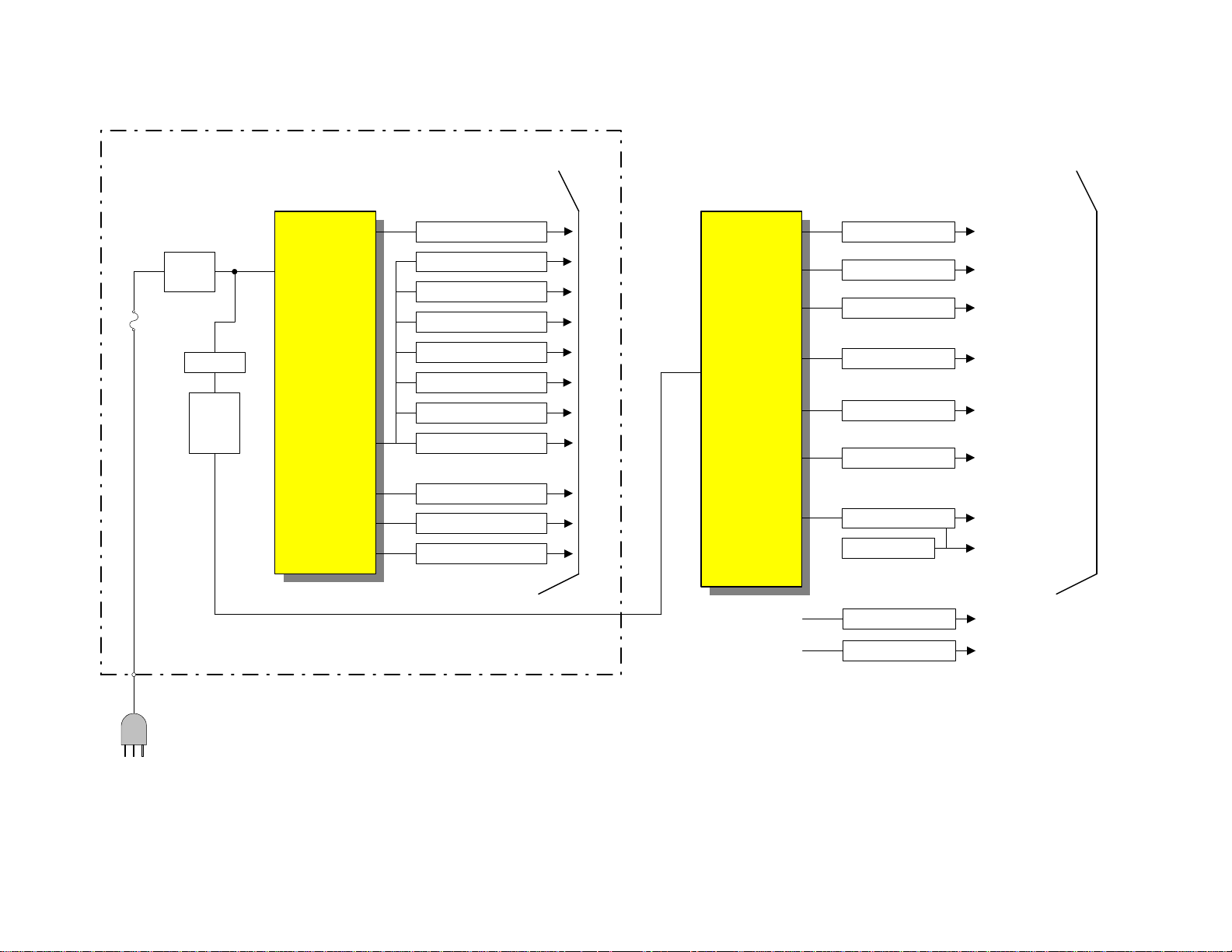
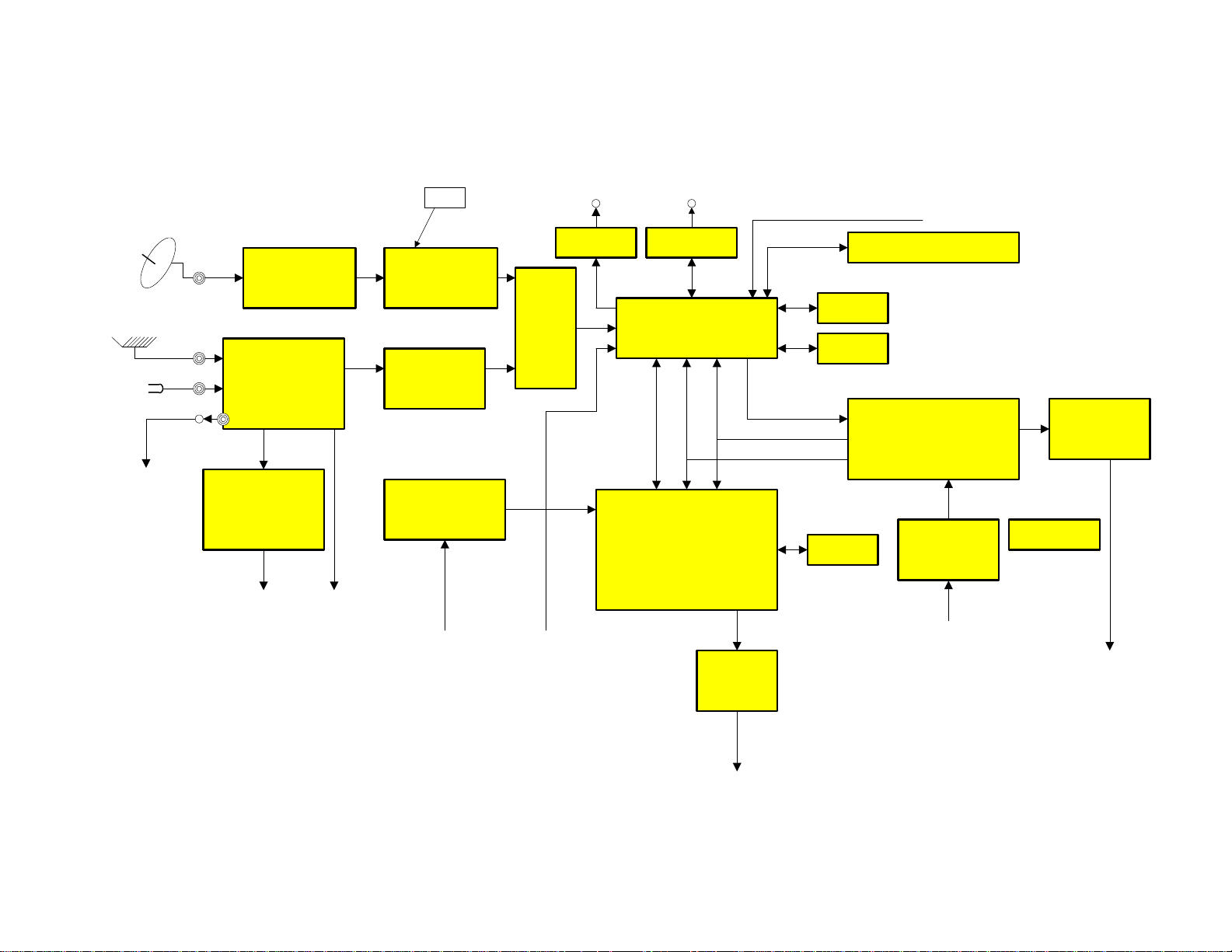
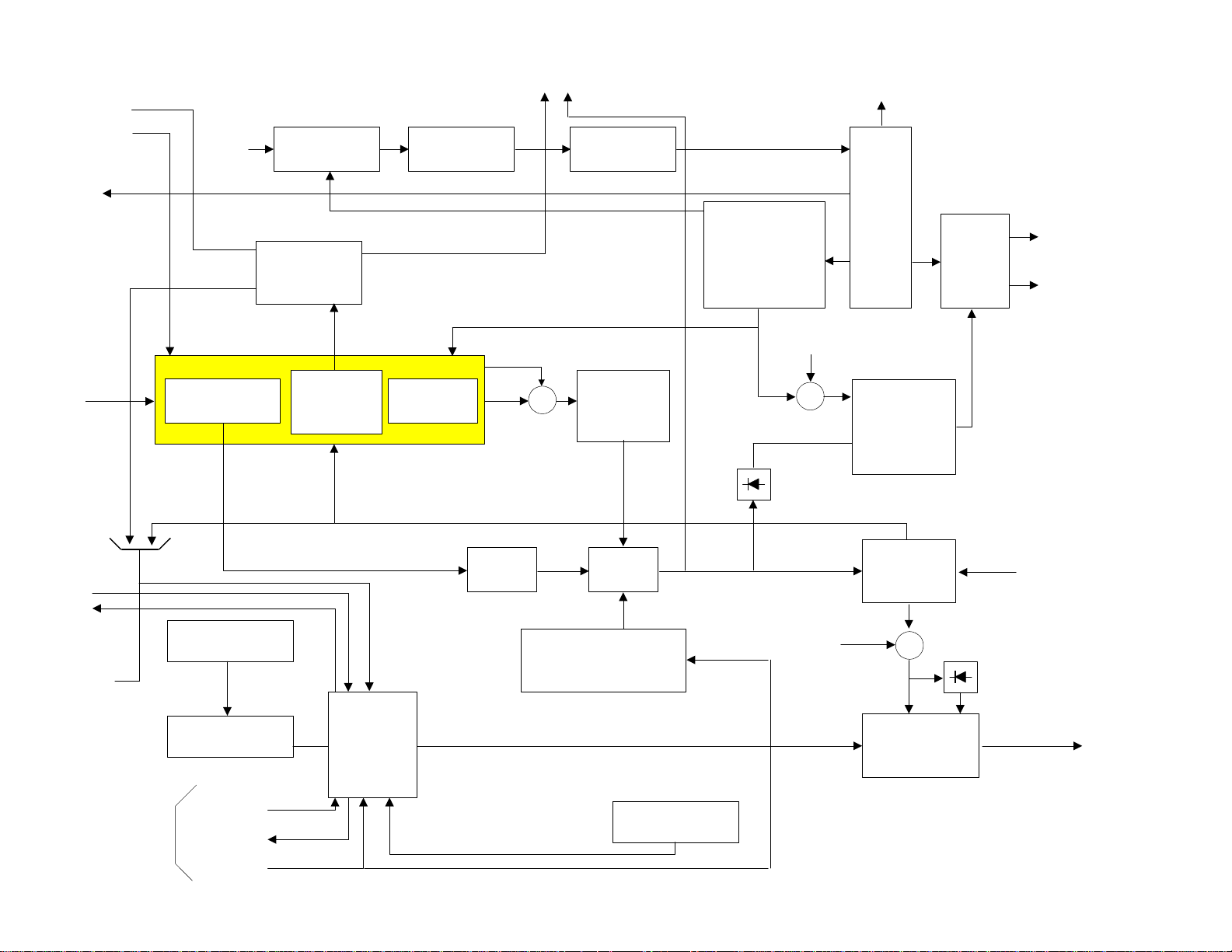
BLOCK DIAGRAM EXPLANATION FRONT END
The 61HDX98B utilizes a non-repairable Front End
Assembly called the DM-1 Module. This module contains the main System control center, NTSC Front
End, Direct TV Receiver and ATSC Tuner. The block
diagram indicates the internal blocks contained within
the Front End Assembly, hear after called the DM-1.
Starting counterclockwise from the upper left.
SATELLITE:
This represents the Direct TV satellite dish connection
to the back of the set.
SATELLITE TUNER/IF:
This is the internal IRD, (Integrated Receiver and Decoder). This receives the satellite signal from the LNB
(Low Noise Block) located on the Dish. This block
converts the signal to a usable signal for decoding.
SATELLITE CARD and SATELLITE LINK
BLOCK:
To receive Direct TV signals, the customer is required
to insert an active Security Card into the back of the
set. This care contains a programmable chip that contains the consumer’s information and the channels that
the consumer is allowed to receive. Also, this card is
used when billing information is retrieved by Direct
TV.
LINK/MIX:
This block passes the particular signal that the customer has decided to view on screen. Either the Direct
TV signal or the ATSC tuner.
TERRESTRIAL:
This indicates the outside antenna the consumer has
erected to receive NTSC signals as well as ATSC signals.
CABLE:
This is the input from the consumer’s cable signal.
HD/NTSC TUNER/IF SPLITTER:
This block receives the Terrestrial signal and dependant upon which source the consumer has decided to
view, processes the signal through the appropriate
tuner.
• HD: Receives the Terrestrial Signal and routes it
to the ATSC tuner. This tuner is capable of receiving all 18 ATSC formats.
• NTSC: Receives the Terrestrial Signal and route
it to the NTSC Tuner.
• The NTSC signal is routed out of this block on the
line labeled Composite Video to the Signal Selector IC which selects the appropriate signal according to the consumer’s choice. Either Tuner,
AVX1, 2 or 3 and/or S-In 1,2 or 3.
• The NTSC audio IF signal is routed to the MTS
STEREO DECODER.
• SPLITTER:
• The splitter routes the NTSC signal out to the RF
Out PinP Tuner path to the PinP Tuner.
MTS STEREO DECODER:
Decodes the NTSC Audio IF signal an decodes it into
Left Total and Right Total. This signal is routed to the
Dolby® Pro-Logic decoder.
HDTV LINK:
This block routs the ATSC signal received by the
ATSC tuner to the Link Mix.
NTSC YUV A/D:
This block receives the NTSC luminance and chroma
signals and converters them to a digital signal to be
utilized by the MPEG VIDEO decoder.
FROM MAIN MICRO:
This is communication in and out for the SubMicroprocessor. Information such as the Selector IC
selection, power on/off commands, etc.., are routed
from the ARM/Transport or Main Microprocessor section.
SD-A/V:
This is the output of the AC-3 digital audio to be used
by an off board AC-3 decoder.
MODEM:
Direct TV polls the Direct TV receiver section through
the customer’s phone lines and determines such things
as Pay for View authorization, customer’s information, Card authorization and billing information.
ARM/TRANSPORT:
The Arm/Transport block receives all signals from Direct TV, ATSC. It also receives the Infrared remote control signals, Front panel Key data, and Slave Microprocessor information. This is the Main Microprocessor section of the DM-1 module. Dynamic RAM and ROM information is processed from Soft ward load into ROM
and determines the state of the Television. Information
from ATSC and/or Direct TV is routed to the MPEG
VIDEO DECODER.
Page 01-03
Page 8

BLOCK DIAGRAM EXPLANATION FRONT END
MPEG VIDEO DECODER, NTSC UPCONVERSION, OSD:
What ever signal is requested by the consumer as the
source for viewing is processed through this block and is
output to the YUV D/As.
YUV/DAs:
This block takes the digital signals provided to it and
converts them to an analog signal which is usable by the
signal processing circuits.
All signals are routed out through the line labeled 2.14
YUV/YIQ, (NTSC Signal up converted to 480P or 2.14
HYPBPR which is the HDTV output as 1080I.
MPEG/AC-3 AUDIO DECODER:
This block processes the audio component from the
ARM/TRANSPORT or the block A/Ds AUDIO, which
is the NTSC audio processed by the Pro Logic decoding
circuit, labeled as 5.1, (Front Left, Front Right, Center,
Rear Left and Rear Right + Sub Woofer audio also called
LFE. Then this block processes the signal and outputs all
audio to the Audio D/As.
AUDIO D/As:
This block is the Digital to Analog converter which converts the digital audio signal sent to it by the ARM/
TRANSPORT block and converts it to a usable analog
signal to be processed by the audio output section.
The audio labeling is comprised of the following:
L/R = Audio Front Left and Right
LS/RS = Rear or Surround audio Left and Right
C/LFE = C for Center and LFE for Sub Woofer, also
called Low Frequency Effects.
Page 01-04
Page 9
DP85 FRONT END
BLOCK
Satellite
Terrestrial
Cable
RF Out
PinP
Tuner
DM-1 Module
SATELLITE
TUNER/IF
HD/NTSC
TUNER/IF
SPLITTER
MTS
STEREO
DECODER
L/R
Composite
Video
SATELLITE
VSB
Satellite
Card
LINK
HDTV
LINK
NTSC YUV
A/D
1HYIQ
SD-A/V MODEM
LINK
MIX
MPEG VIDEO
UPCONVERSION
From
Main
Micro
PhoneSD-
ARM/
TRANSPORT
DECODER
NTSC
OSD
YUV
D/As
IR from Ft. Panel
Dimmer, AD, Key In
DRAM
ROM
Data
Address
Handshake
SRAM
From Main Micro
NRSS/ISO7815
MPEG/AC-3
AUDIO
DECODER
5.1 Audio
Digital
A/D's
AUDIO
L/R
AUDIO
D/A's
EEROM
L/R
LS/RS
C/LFE
Page 01-05
2.14YUV/YIQ
2.14 HYPBPR
To 2H Video Circuit
Page 10

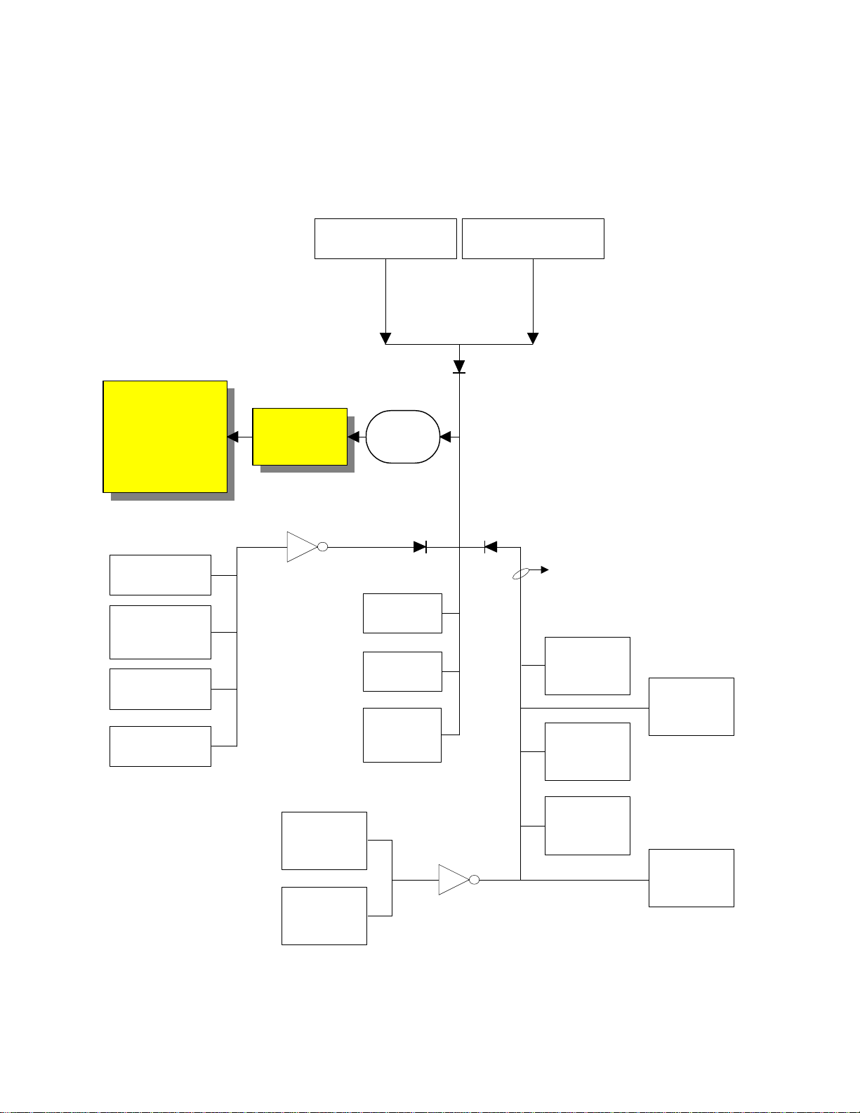
BLOCK DIAGRAM EXPLANATION A/V SELECTOR
C. VIDEO (MAIN) and R/L (AUDIO MAIN):
NTSC Video and NTSC Audio is routed from the
DM-1 Block diagram. They are shown in the Block
Diagram as one line, but they are separate signals.
Anytime a signal is routed from the DM-1 or going to
the DM-1 module, they must be sent through a DM-1
I/F block. This block reduces the noise by a noise cancellation process. This process uses the output of a
comparator and routes the output back to the negative
input to subtract the noise. It also level shifts the signal
to make it useable by the circuit to which it is routed.
DM-1 I/F BA4558:
This is the noise cancellation and level shift block.
AUDIO/VIDEO SELECTOR TA8851BN:
This is the selector IC. Dependant upon the customer’s
viewing preference, the DM-1 will communicate via
I2C bus communications and select the NTSC signal
which is sent to the demodulator. The demodulator
prepares the NTSC signal for the DM-1 module.
This IC selects the following inputs;
Main tuner
Video One, Two or Three
S-In One, Two or Three
PinP Video and Audio outputs. This can be any of the
input provided above except the PinP has it’s own
tuner.
Note: PinP isn’t available when the customer has selected Direct TV or ATSC as it’s source. This is because, as will be shown later, the PinP Video is super
exposed upon the NTSC video only.
Any video source selected for the Main picture will be
routed to the 3D Y/C module.
Note: There are NO Component inputs on this set.
Page 01-06
Page 11
C. Video (Main)
R/L (Audio Main)
A/V SELECTOR BLOCK DP85
CHASSIS
TERMINAL P.W.B.
DM-1
I/F
B4558
Comp. Video (Main) R/L (Main)
RF from DM-1
Tuner U001
VT+33V
Video 4 V4, S4, L/R4
PinP Video and
Selected L/R
(NTSC Main Audio)
+5V +9V
PinP
Lock
Clock
Data
Enable
MonoAudio
PinP
Video
Mono
AUDIO/VIDEO
SELECTOR
TA8851BN
PinP Video
to PinP Unit
Video D YC
To 3DYC
9V
I2C
PinP L/R Out
To Audio Out PWB
Video One In
Video Two In
V1 S1 L/R1
V2 S2 L/R2
V3 S3 L/R3
Video Three In
Page 01-07
Page 12

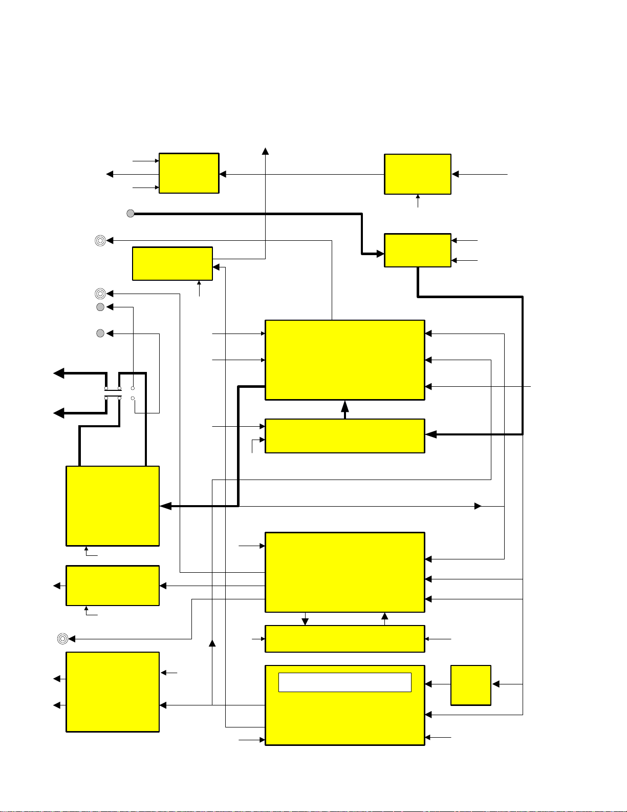
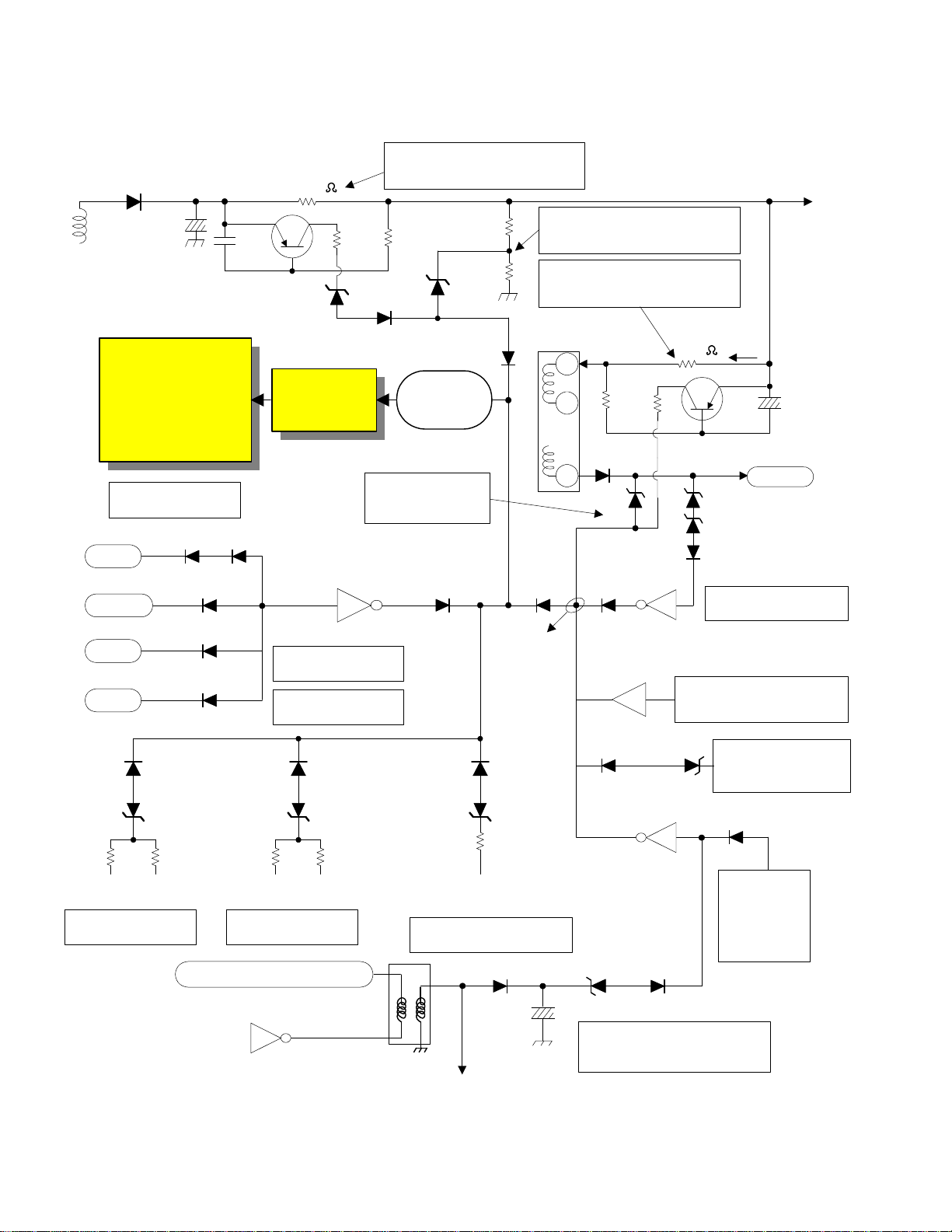
BLOCK DIAGRAM EXPLANATION
SYSTEM CONTROL AND SIGNAL PROCESSING
MAIN VIDEO FROM SELECTOR IC:
At the bottom left hand side is shown the Main Video
from Selector label. This is the NTSC video from the
selector IC. This is routed to two blocks.
3D Y/C:
The 3D Y/C separates luminance from the chroma. It
also add the 3D effect, (if the 3D Y/C is turned on
within the menu). Noise is canceled and the two separate components are output to the Video/Chroma Demodulator.
VIDEO/CHROMA DEMODULATOR:
This IC decodes the signal down to it’s Luminance and
Chroma. components and outputs it as 1HYIQ.
DM-1 I/F:
Noise cancellation and level shifting preparing the signal for the DM-1 module.
1HYIQ:
1HY = Standard NTSC format luminance. (Also
known as 480I).
I and Q = Standard NTSC format, demodulated
chroma components.
SYNC DET.:
Separates the Sync signal from the composite video signal.
SYNC DET.:
This block outputs composite sync to the PinP unit which
is used for timing for display. This is specifically related
to the Demodulator, D/As and Read/Write clock. The
Read/Write clock also is controlled by the frequency of
the Subcarrier also called fsc.
The Composite sync is also sent to the DM-1 on the line
labeled as 1H Composite Sync. The DM-1 uses this signal for OSD positioning, auto channel detection and AFC
loop activation.
TV uCOM MICROPROCESSOR:
This is the slave Microprocessor or Sub-Microprocessor.
This IC is in constant communications with the DM-1
module. The slave uP. Receives or outputs the following
signals;
HBLK: = Input; this is the Horizontal Blanking signal.
Used for Service OSD signal creation timing.
S.WIDE: = Output; when the customer watches regular
NTSC 4X3 aspect source, they have a choice of viewing
the signal in one of 4 ways.
Normal: This will display a standard 4X3 picture
with black panels on each side of the picture.
Fill: This will expand the picture to fill the screen.
The top and bottom will be cropped.
Full: This will expand the picture side ways and fill
the screen. However the picture will be non-linear.
Smooth Wide: This will keep the center of the picture linear and stretch the outside edges to fill the
screen.
With the four choices above, the DM-1 module controls
the signal for 3 of them; Normal, Fill and Full. However,
during Smooth Wide, the deflection circuit is switched to
perform the stretching of the sides. The slave Microprocessor outputs S.Wide during this time.
CUT OFF: = Output; labeled as V. Stop, during the Ser-
vice adjustments for Cut Off, (Screen Background controls), the vertical must be collapsed. This output causes
the B+ to the vertical output IC front end to be grounded
and grounds the vertical trigger pulse called V. Saw.
D. SIZE: = Output; labeled as Digicon Size, during
Smooth Wide mode, the Digital Convergence Unit, hear
after called DCU, must know that the set is in the distorted deflection mode. This signal tells the DCU just
that.
MAGIC SW: = Input; when the customer presses the
Magic Focus button on the control panel, the DCU notifies the slave micro. That it is busy performing Magic
Focus. The slave micro. Notifies the DM-1 module and
the DM-1 module ignores infrared pulses from the remote control.
CLOSED CAP. DATA: = Input; This input receives the
composite sync signal and decodes the Closed Caption
Data. (Data Slice line 21) and the communicates with the
DM-1 Module. The DM-1 Module actually introduces
the Closed Caption Characters into the Video stream.
F. PANEL: = Output, Dependant upon the customer’s
menu selection, will determine the IRE level of the side
panels when 4X3 Normal mode is used. By raising the
side panel IRE levels, the 4X3 picture won’t burn in the
CRT’s.
MAIN SYNC DET: = Input; this is used for detecting the
Closed Caption Data. This information is routed to the
DM-1 module for OSD generation. NOTE: the submicro. Doesn’t produce OSD characters for Closed Caption.
PinP SYNC DET: = Input; PinP tuner sync is routed to
the sub-micro. And is used during PinP tuner channel
Page 01-08
Page 13

BLOCK DIAGRAM EXPLANATION
SYSTEM CONTROL AND SIGNAL PROCESSING
selection to activate AFC.
MAIN SYNC DET. = Input; This input is used for Service OSD positioning and Auto Programming channel
detection.
PinP SYNC DET. = Input; This input is used for judgement of the Slave Microprocessor to determine the AFC
Loop activity of the PinP Tuner.
MUTE (Audio): = Output; during channel change, external video selection with no input, power up or power
off, and loss of Vertical Blanking, the audio and video
are muted.
V.MUTE (Video): = Output; during child lock, channel
change, or power on/off, the video is muted.
POWER: = Output; when the front power button or the
remote power button is pressed, the DM-1 module notifies the sub-micro. And the sub-micro. Outputs a power
on/off command to the relay driver Q-007. Outputs high
for ON and low for OFF.
OSD & OSD BLK: = Output, this is the on screen characters for the Service Menu only. OSD Blk is OSD
blanking. This cleans us the video where the OSD is to
be inserted.
HV BLK: = Input; this inputs are utilized by the Microprocessor for Service OSD positioning.
HV BLK PH: = Output; during Service Adjustment and
in the NTSC normal mode. This picture doesn’t fill the
screen. The areas on the side of the picture are called
Side Panels. This can be adjusted. The HV BLK PH,
controls the timing of the side panel OSD outputs.
SIDE PANEL APL FROM 2H VIDEO PWB: = Input;
the Microprocessor receives a pulse created within the
2H video PWB. This pulse represents the timing pulse
for the Side Panel OSD production.
Blocks continued;
OSD MIX: Only the Service menu OSD is output from
the Slave Microprocessor. The Digital convergence unit
puts out OSD characters as well. This characters product
the Service Grid and other text during Digital Convergence adjustments and/or Magic Focus. The two OSD
sources are received by the OSD Mix. This is comprised
of a quad Or Gate and outputs the signal to be superimposed upon the video signal path from the DM-1 Module.
PinP VIDEO FROM SELECTOR IC: The video from
the PinP tuner is routed to the PinP unit and the Sub Microprocessor for Closed Caption decoding.
Page 01-09
Page 14
DP-85 CHASSIS SYSTEM CONTROL & SIGNAL PROCESSING
BLOCK
PinP
Unit
PinP
Video
3D
Y/C
Unit
Y/C
Y/C
H Sync
V Sync
1 H Composite
Sync
I2C
Closed Cap. Data
Digital OSD / Busy
TV uCOM
Microprocessor
HBlk
S. Wide
Cut. Off
D. Size
Magic Sw.
F Panel
Main Sync Det
PinP Sync Det
Mute (Audio)
V.Mute (Video)
Power
OSD & OSD Blk
for Service Menu
OSD RGB Ys
OSD
MIX
+
RGB Ys
OSD
AD8056
VIDEO/
CHROMA
DEMOD
YIQ
Mix
YIQ
1HYIQ
DM-1
I/F
Clamp
I2C
Sync Det.
Y
MEMORY
Sync Det.
PinP
Sync Det.
I2C
HV BLK
H BLK PH
Side Panel
APL
from 2H
Video PWB
Page 01-10
PinP Video from Selector
IC
PinP V
SIGNAL P.W.B.
CCD Video
CCD Video
PinP
Main Video from Selector IC
Main
Page 15

BLOCK DIAGRAM EXPLANATION 2H VIDEO
The 2H Video PWB is similar to the Rainforest circuits used in the past. The YUV/YIQ
(480P) and/or the Y-PR/PB (1080I) is routed
through another DM-1 Interface IC for noise
cancellation and level shifting and into the
Rainforest chip, IX01. Here the signal is prepared for the CRT’s. Pedestal level detection,
Chroma preparation, OSD RGB from either
the DCU or the Slave Microprocessor is input
here.
Remember that the OSD for Customer usage
such as the Channel numbers, clock, Main
Menu, etc.. is generated by the DM-1 Module.
Also, ABL controls the brightness and
Contrast; as well as the color level at this
chip.
The Velocity modulation control signal is
produced from the Rainforest IC. This signal
is a representative of the Peak White components of luminance and drives the Velocity
Modulation coils on each CRT.
Page 01-11
Page 16
2 H VIDEO BLOCK DP-85
CHASSIS
2H VIDEO P.W.B.
OSD RGBABLI2C
YUV/YIQ/
Y PB PR
2.14 HV SYNC
YUV/YIQ/
Y PB PR
2.14 HV SYNC
+9V
+5V
DM-1
I/F
+5V -5V
RGB PROCESSOR
TA1276AN
Clamp H/V Blk.
YUV RGB
Y
YUV
YIQ
YPBPR
APL
DETECT
RGB
VM
SPANEL
Side Panel
APL
2.14 HV SYNC
CLAMP
GEN.
Clamp
HV. Blk.
Gen.
HBLK PH
HV Blk
+9V
2.14 SYNC
Page 01-12
Page 17

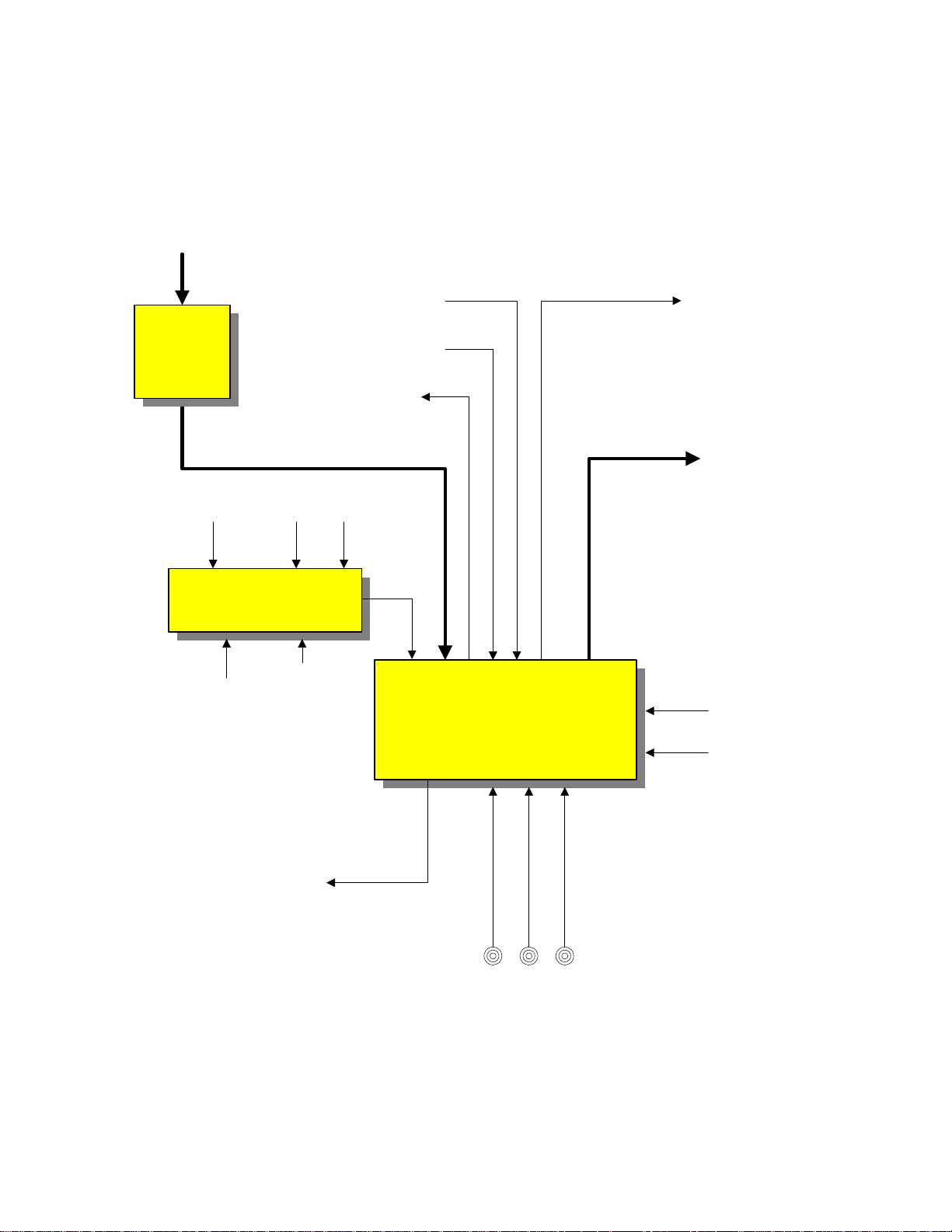
BLOCK DIAGRAM EXPLANATION DEFLECTION BLOCK
The 61HDX98B deflection circuit differs from conventional Hitachi product. It utilizes in a sense, two
horizontal output circuits. One for Deflection and on
for High Voltage. The notations around the Block diagram will be described in a counter clock wise fashion
as best a possible.
CUT OFF:
Cut of collapses the Vertical circuit during I2C Bus
alignments, during CRT Set Up.
I2C:
Communication from the Sub Microprocessor I001
during sweep variations due to Standard/NTSC 480P
mode and 1080I High Definition mode.
ABL:
ABL voltage is generated by monitoring the current
through the flyback transformer. This voltage will
fluctuate down when the scene is bright and up when
the scene is dark. The ABL voltage will manipulate
the screen brightness and contrast to prevent blooming
under these conditions.
HV SYNC:
The composite sync is routed into the Sync processor
which determines the sweep condition for the signal
being provided.
H and V BLK:
Horizontal and Vertical Blanking is developed within
the Deflection circuit. The Horizontal Blanking pulse
operates around 13V P/P and is produced by taking a
sample pulse from the Deflection transformer T752.
The Vertical Blanking pulse is generated from the
Vertical output IC, I601 pin 7. This pulse normally
operates at 23V P/P.
IR:
The Infrared Pulses coming from the remote control
are routed through the Deflection PWB to the Digital
Convergence Unit. During DCAM (Digital Convergence Adjustment Mode), the Remote Control provides manipulation pulses for the DCU.
DIG RGB BUSY:
This indicates Digital RGB and BUSY.
Digital RGB represents the on screen characters produced by the DCU for generating the Digital Convergence adjustment grid and text produced during certain conditions such as Magic Focus, Sensor Initialization, Data Storage, etc…
Busy notifies the sub Microprocessor I901 which in
turn notifies the DM-1 module that the DCU has entered the DCAM. During this time, the DM-1 module
ignores the remote control commands.
MAGIC SW:
When the customer presses the Magic Focus button on
the front of the set, it produces a command for the
DCU to begin the Magic Focus process.
D SIZE:
Digital Size is a control signal for raster enlargement
when MAGIC FOCUS is operated. Raster enlargement is required for the MAGIC FOCUS PATTERN
to hit the photo sensors.
This signal is output from DCU and input to the Sub
Microprocessor I901. The Sub Microprocessor controls the I702 on the DEF.SUB PWB) for enlarging
raster size.
In case of AP-85, this control signal is called "A.
SIZE". It's the same function between DIG.SIZE and
A.SIZE.
S WIDE:
Smooth Wide is a condition entered through the Menu
by the customer while watching an NTSC 4X3 aspect
video source and the customer wants to fill the screen.
TO CONVERGENCE YOKES:
The DCU provides compensation signal for deflection
abnormalities to the convergence output IC. The Convergence output IC in turn, amplify the signals and
rout them to the convergence yokes.
+26V, 26VP and RETRACE PULSE:
The positive 26V and the negative 26V is routed to the
Deflection transformer I752. They enter the transformer as a pure DC voltage. A 15V P/P horizontal
pulse is added to the DC voltage and leaves as +26VP
and –26VP. From here these voltages are routed to the
Convergence output section and they are rectified.
They become +33V and -33V respectively. This process prevents the need for another power supply.
+B 130V:
The Deflection transformer receives the 130V V1 DC
source.
DF OUT:
Generated from the I702 on the Sub Deflection PWB
and the Horizontal Blanking pulses, a Dynamic Focus
waveform is created. This is a parabolic waveform that
Page 01-13
Page 18

BLOCK DIAGRAM EXPLANATION DEFLECTION BLOCK
is superimposed upon the static focus voltage to compensate for beam shape abnormalities which occur on
the outside edges of the screen because the beam has
to travel further to those locations.
HV PARABOLA:
Described above.
SCREEN 700V: 700V Supplied to the screen grids on
the CRT’s.
FOCUS 9KV:
Focus voltage supplied to the CRT’s.
32Kv HV:
32,000 volts DC supplied to the CRT’s anodes.
TO DEFLECTION YOKES:
Horizontal and Vertical deflection wave forms driving
the deflection yokes.
INTERNAL BLOCKS DESCRIPTION
HV CONTROL:
The uPc1344C IC generates the horizontal drive signal
utilized by the High Voltage circuit. The HV control
IC receives it’s locking pulse from the Deflection circuit. A feed back voltage is sampled from the High
Voltage Regulation Detector circuit and compared
with a reference voltage to maintain an accurate 32KV
on the CRT’s.
VERTICAL OUTPUT:
The vertical output utilized in the 61HDX98B operates
differently from previous chassis. This circuit utilizes
a +13V and a –13V to generate the waveform to drive
the vertical deflection yokes. A pump up circuit is utilized to product the retrace pulse for the vertical deflection yoke. It’s at this time when a higher pulse is
needed because the beam has to travel from the bottom
of the screen to the top very rapidly. The vertical output IC receives it’s trigger pulse from the ramp generator.
SYNC PROCESSOR:
The Sync Processor located in I702 on the Sub Deflection PWB, detects the horizontal sync rate for the displayed signal, either 480P or 1080I.
VERTICAL RAMP GENERATOR:
I702 on the Sub Deflection PWB generates the Vertical Saw signal. This signal is controlled by several
factors. The Sync Processor detection and I2C data
communication.
DIST CONTROL:
Distortion control is another signal produce by I702
and sent to the Side Pin cushion circuit. These compensation parabolic wave forms are combined with the
horizontal circuit to compensate for Side pincushion
errors.
H-SIZE SIDE-PIN CONTROL:
This circuit generates the Side Pincushion Distortion
compensation pulse which is impressed onto a coil
located in the output side of the Deflection Output section and compensates for Pin Cushion distortion.
HORZ. DRIVE and HORZ. OUT:
This circuit comprises the Drive and Output for the
Deflection output circuit.
S-CORRECT (SMOOTH MODE):
During Smooth mode, the deflection circuit is manipulated so that the outside 1/3 of the picture is stretched
to fill the screen. The center 2/3 of the picture is left
undistorted. When an S Wide signal is received, a capacitor is switched off on the output side of the Deflection output circuit.
PHOTO SENSOR:
There are 8 sensors located on the internal outside
edges of the cabinet. These Photo Cells receive the
light patterns being generated during MAGIC FOCUS
or SENSOR INITIALIZATION and deliver this voltage to the Sensor Distribution circuit.
SENSOR DISTRIBUTION:
This represents the amplifiers that receive the Photo
receivers (Photo Cells) inputs during Magic Focus operation.
DIGITAL CONV. UNIT:
This is the Digital Convergence Unit. This is a nonrepairable unit. It contains the distortion compensation
wave form generation circuits, RAM, ROM and D/A’s
for the convergence circuit.
SERVICE SWITCH:
When the set needs a convergence alignment, the Ser-
Page 01-14
Page 19

BLOCK DIAGRAM EXPLANATION DEFLECTION BLOCK
vice Switch is pressed. This switch is located on the
deflection PWB. By removing the front speaker grill,
the Service Technician has access to this switch.
CONV. OUT:
The Convergence output block represents the two (2)
Convergence output IC’s. These two IC’s contain the
amplifiers for the Red, Green and Blue convergence
outputs.
HDT T752:
Represents the Deflection output transformer. By
separating the Deflection circuit from the High Voltage, any distortions that would be generated by fluctuations within the High Voltage won’t be visible
within deflection.
DYNAMIC FOCUS OUT:
This circuit amplifies the parabolic signals provided
by the Deflection circuit and I702 on the Sub Deflection PWB and impresses these wave forms onto the
static DC voltage use for focus. This keeps the beam
as sharp or focused as possible in the corners of the
screen.
HIGH VOLTAGE REGULATION DETECTOR:
This circuit monitors a feed back voltage produced
from the High Voltage Flyback transformer and routes
an output signal to two circuits.
1.) A sample voltage is sent to the Horizontal Driver
IC for regulation of the High Voltage and;
2.) If the High Voltage climbs too high, a shut down
signal is produced to shut down the power supply until
a repair can be made.
FOCUS PACK:
The focus pack receives the Focus voltage and the
High Voltage and distributes them to the CRT’s.
FBT TH01:
Is the main Flyback Transformer producing High
Voltage.
Page 01-15
Page 20
Cut Off
I2C
HV Control
(uPC1344C)
DP-85 DEFLECTION BLOCK
HV DRIVE
(MC3415IP)
DIAGRAM
To Deflection YokesTo Deflection Yokes
HV OUT
(IMB12-140)
ABL
32Kv
HV
High Voltage
Transformer
HV Sync
V Blk
IR
Dig RGB
Busy
HV Blk
Page 01-16
ABL
H Blk
From uP
C
2
I
SYNC.
PROCESSOR
H Drive
PHOTO
SENSOR
/ 8
SENSOR
DISTRIBUTION
Magic SW
D Size
VERTICAL
OUT
LA7648
VERTICAL
RAMP
GEN.
Busy
Dig RGB
8
/
DC couple
/
S Corrected
V-SAW
H Blk
IR
DIGITAL
CONV.
UNIT
3
DIST.
CONTROL
HV Blk
6
/
V Parabola
Saw
Modulator
HORZ.
DRIVE
Size Regulation
Control
H-SIZE
+
Diode
(SMOOTH MODE)
SIDE-PIN
CONTROL
HORZ.
OUT
S-CORRECT
SERVICE
SWITCH
REGULATION
Vcp
S Wide
VOLTAGE
DETECTOR
Parabola
1100V
+26V,
HV
+
26V
FBT
THO1HIGH
FOCUS
PACK
Focus
12Kv
DYNAMIC
FOCUS OUT
2SC4686X3
Deflection Transformer
HDT
T752
+
CONV.
OUT
DF
Out
Retrace Pulse
34v, -34v
6
/
To Convergence
3
Focus
/
(9KV)
Screen
/
(700V)
3
+B (130V)
Yokes
S Wide
Page 21
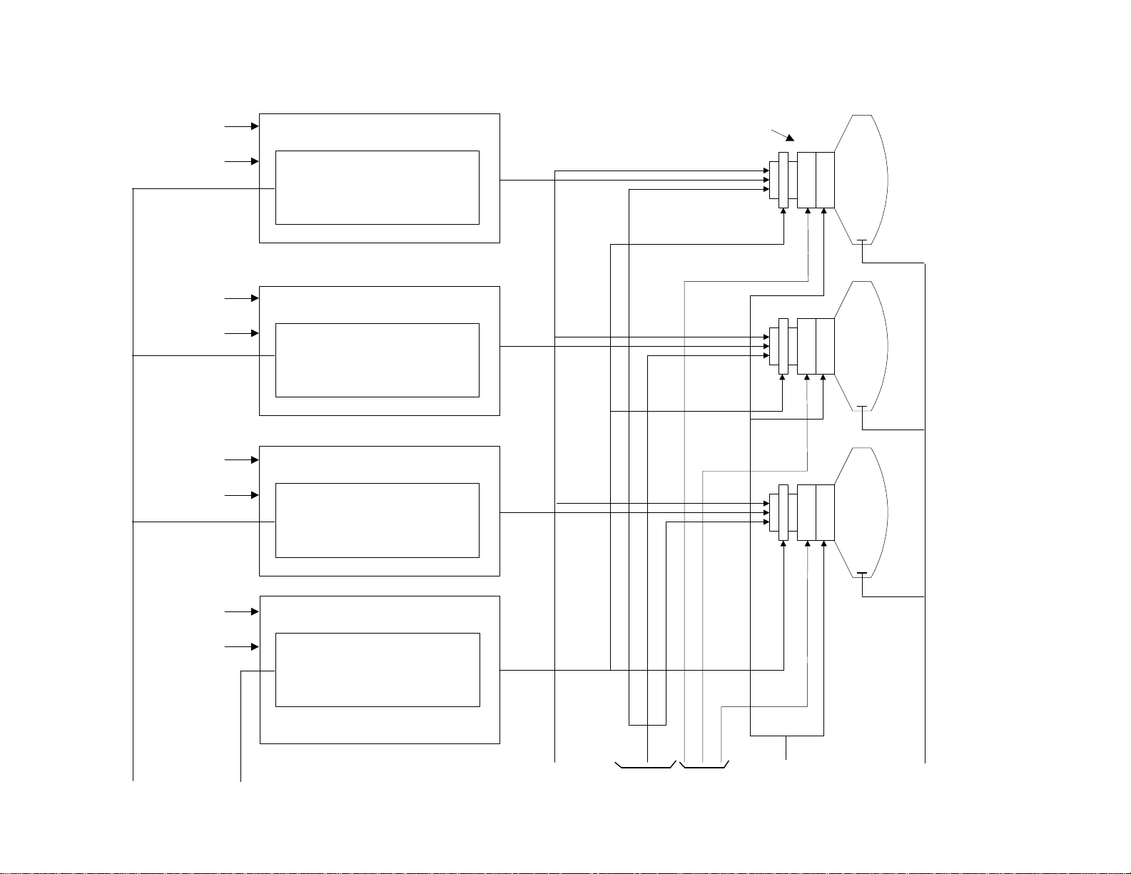
220V
12V
CPT P.W.B. (R)
VIDEO OUTPUT
AMP
DP-85 CRT PWB BLOCK DIAGRAM
Beam Shape, Beam Alignment,
Focus, VM Coil,
Deflection and Convergence Yokes
R
220V
12V
220V
12V
220V
26V
CPT P.W.B. (G)
VIDEO OUTPUT
AMP
CPT P.W.B. (B)
VIDEO OUTPUT
AMP
VM OUT P.W.B.
VM OUT
G
B
Page 01-17
RGB
VM
SCREEN
FOCUS CONV.
Def.
Yokes
30KV
HV
Page 22
AUDIO OUTPUT SECTION DP-85
CHASSIS
To
Headphone
Jack
L/R
From DM-1
TL/TR
Fixed Vari
Out L/R
FR Ext
Out
FL Ext
Out
FR
to Spk
FL
+9V
-9V
DM-1
I/F
Headphone
Amp
+9V
+9V
Clock
Data
I2C
HL/R
HL/R
L/R LS/RS/C/LFE
TL/TR
CONTROL
Graphic Equalizer
Perfect
Volume
+9V
DM-1
I/F
L/R
RL/RR
PinP L/R
L/R
From
Audio/Video
Selector IC
+9V
9V
PinP L/R
From
Selector IC
L R
Front
Audio
Amp
26V
Center
Audio Amp
21V
Sub Woofer
Rear
R
Audio
L
Amp
FL/R
28V
Clock
Data
RL/RR
HP L/R
I2C
+9V
I2C
L/R
C
LFE
CONTROL
Graphic Equalizer
Headphone L/R
CONTROL
FL/FR
L/R
C/LFE
+9V
L+C
R+C
+9V
L/R
C
LS/RS
Page 01-18
Page 23
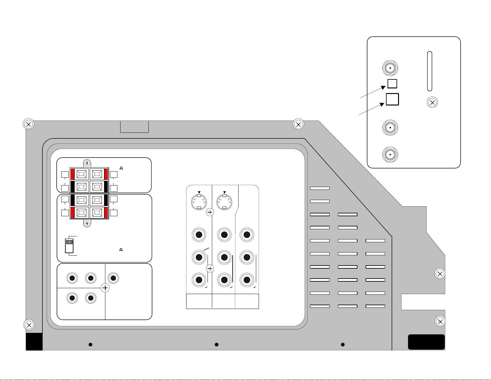
DP-85 REAR PANEL (61HDX98B)
DSS IN
DM-1 MODULE
Rear Panel 1
SMART
CARD
SLOT
AC-3 Jack
Telephone
Interface
ANT B
ANT A
REAR SPEAKER
8 ONLY
+
R
-
-
R
+
INT.
EXT.
+
L
-
-
L
+
FRONT SPEAKER
8 ONLY
S-VIDEO S-VIDEO
VIDEO
(MONO)
VIDEO VIDEO
(MONO)
L
(MONO)
L
L
Page 01-19
TRANSMITTER
OUT
R L
R L
FIX/VARIABLE
OUT
LFE/SUB
WOOFER OUT
R
AUDIO AUDIO AUDIO
INPUT 1 INPUT 2
R
INPUT 3
R
Page 24
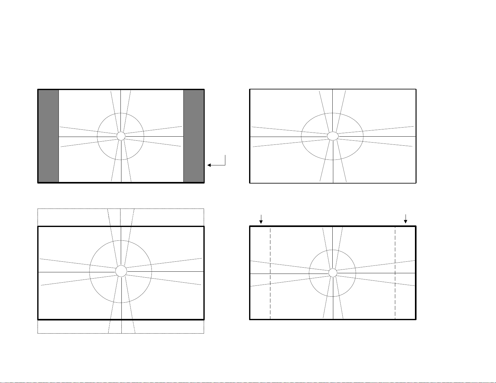
DP-85 CHASSIS 4 MODES TO DISPLAY A (4x3) IMAGE ON (16X9) DISPLAY
DM-1 Module controls the video content for Normal, Full and Fill modes,
while the deflection circuit is manipulated for the Smooth Wide mode.
NORMAL MODE (4x3) FULL MODE (4x3)
Side PanelSide Panel
Normal Mode 4X3 with Black Mask (Linear)
FILL MODE (4x3)
Cropped
Slightly
above
black
to avoid
4X3
burning
an image
Full Mode 4X3 Stretched to fit (Non-Linear)
Stretched Stretched
SMOOTH WIDE MODE (4x3)
Linear
Linear
Page 01-20
Cropped
Fill Mode 4X3 Cropped (Linear)
Deflection Circuit remains at 33.75KHz for all modes, (NTSC & SDTV = 540P, HDTV = 1080I. (Labeled in schematic as 2.14H)
Smooth Wide Mode 4X3 Center (Linear)
Outside edges Stretched to fit (Non-Linear)
Page 25

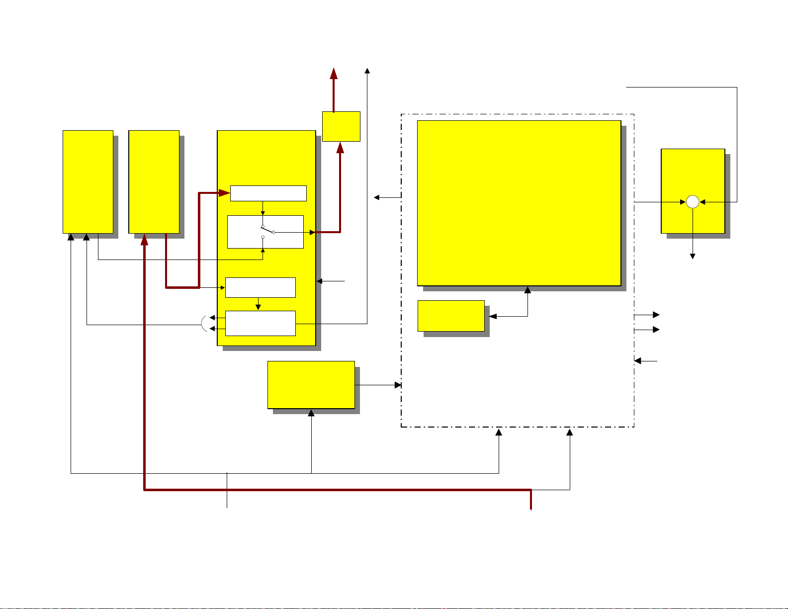
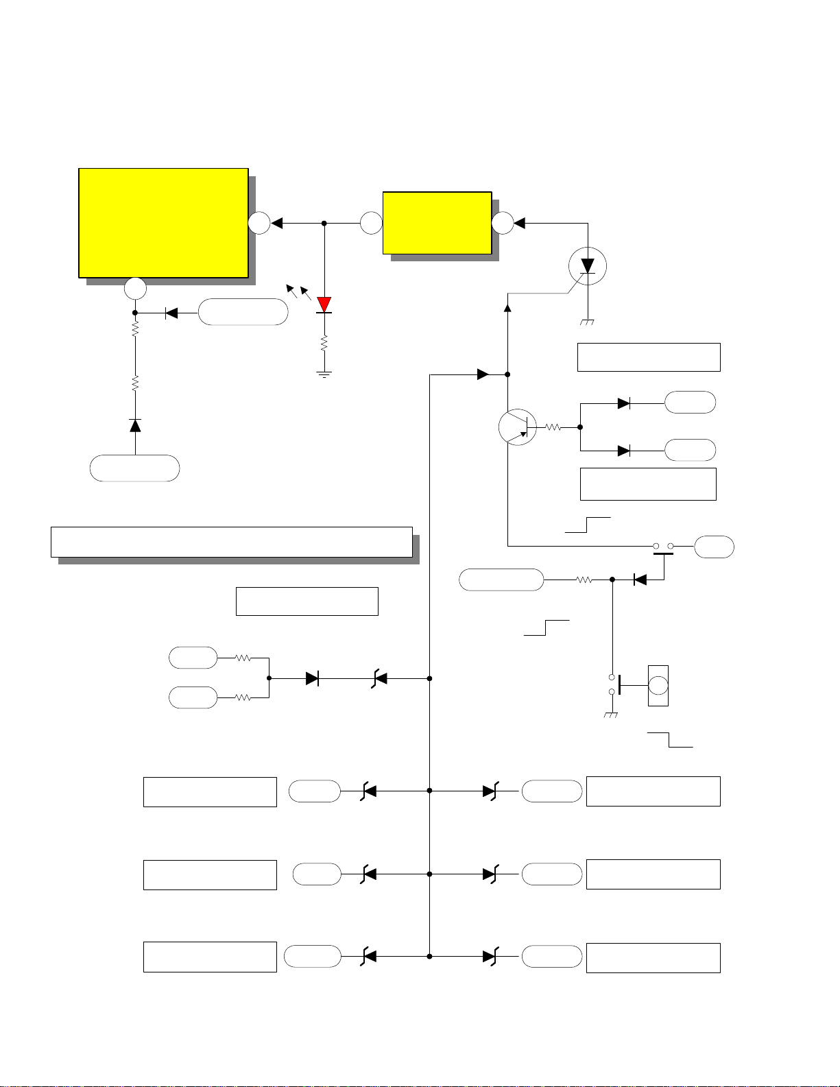
DP-85 DIGITAL CIRCUIT POWER SUPPLY SHUTDOWN BLOCK
I901
ShutDown Pin (7)
I905
on Power Supply
7 3 2
Photocoupler
Driver &
Output IC
Shut Down SCR
+5V Short Det.+3.3V Short Det.
+9V Short Det.-5V Loss Det.
+3.3Vs Too Hi Det.+5V Too Hi Det.
+5Vs Too Hi Det.+9V Too Hi Det.
+12VS Too Hi Det.D3.3V Too Hi Det.
Page 02-01
Page 26
DP-85 DIGITAL CIRCUIT POWER SUPPLY SHUTDOWN DIAGRAM
DIGITAL & SIGNAL
I901
ShutDown Pin (7)
on Power Supply
Driver &
Output IC
5
R907
D905
POWER SUPPLY SHUT-DOWN
Active High
7 3 2
I905
Photocoupler
D908
Run B+
R919
Red LED
Shut Down
Identification
DIGITAL & SIGNAL
POWER SUPPLY SHUT-DOWN
Active Low
Q913
ShutDown
S.C.R.
TV 5V Short Det.
R908
D964
1/2 AC In
Start Up B+
NOTE: +12VS is the same as A12V and STBY12V
No Start Up B+ = Off
Normal = Glowing
Blinks during Shutdown because
of the internal current draw.
15.1V ~ 22.5V pin 5 I901
-5V Loss Det.
R975
-5VS
R976
+5VS
D974
TV 5V Too Hi Det.
+5V +3.3Vs
Q917
D972
+5V
D925
+9V
TV 9V Short Det.
On
STBY +12V
Off
R9A
0
E C
B
Vcc
Q916
D958
On
D953D952
Off
Q914
B
Off
PQS1
Power5
On
C
E
D934
+3.3V Too Hi Det.
TV 9V Too Hi Det.
D3.3V Too Hi Det.
+9V
D3.3V
D975
D938
D933
D936
+5Vs
+12VS
+5V Too Hi Det.
+12VS Too Hi Det.
Page 02-02
Page 27
Audio
F/R 28V
R927
DP-85 CHASSIS L.E.D. (VISUAL TROUBLE DETECTION) DIODES
(SUB POWER PWB) DIGITAL POWER SUPPLY 10 GREEN L.E.D.s and 1 RED L.E.D.
(11 Total L.E.Ds. for visual trouble sensing observation)
LNB Power
Audio
Center 21V
R928
TV 9V
R945
TV 5V
R9E3
+12VS
R956
13V/19V
R939
+5VS
R965
-5VS
+3.3VS
R966
D3.3V
R972
R969
D919
D908 is a RED L.E.D.
Off = No I901 B+
On (Mid) = I901 B+
On (Bright) = Shutdown
Page 02-03
D920
D908
R919
D930
Osc B+
1.9V
D971
ALL GREEN L.E.D.s
D928 D924
Start Up or Run
24.2V
5
I901
Driver/Output IC
100% Dead Time &
7
IC B+ Detection
R916
D943
24.2V
1.9V
D962 D945
D947
Vcc
I905
4
3
I905 Shutdown
Photocoupler
12 Shut Down
Inputs
1
2
Q913
Shutdown
SCR
Page 28
DP-85 DIGITAL CIRCUIT POWER SUPPLY DISTRIBUTION DIAGRAM
Page 02-04
AC Plug
AC Input
FUSE
F901
Noise Filter
L901, 2, 3
Rectifier
D901
Protector
E992: 7K
Switching
Control
I901
D908:
Protect Red LED
To
Deflection
Power Supply
Protection
Block
Live Cold
Switching
Transformer
T901
Feedback
I904
Protect
I905
AC Clock
I906
RELAY
S901
Relay
S902
Relay
S903
DP86
Only
AC Clock
60Hz
Protector
E994 : 7K
Protector
E995 : 7K
Protector
E996 : 5K
Voltage
Control
24, 5V
Q915
Rectifier
+28V : D911
Rectifier
+21V : D912
Rectifier
+35V : D918
Rectifier
+24V, 5:D914
TV ON/OFF
Switch
Q914, Q918
TV Main ON/OFF
ON = LO
OFF = Hi
D919 : F28
D920 : C21
A12V
Regulator
+12 : I907
Regulator
TV9V : I908
Regulator
TV5V : I914
Protector
SCR: Q913
= RED OR GREEN L.E.D.
STAND BY +12V
D928 : +12V
D930 : TV9V
D971 : TV5V
Short Circuit
Detector
REAR +28V
CENTER +21V
D
D
"D"
D925:
<4V
D925:
<4V
Audio
+28V
Audio
+21V
33VS :
D936 : >14.7V
ZD
D975 : >10.8V
ZD
D933 : >6.7V
ZD
Over
Voltage
Detector
+33V
+12VS
+9V
+5V
Page 29
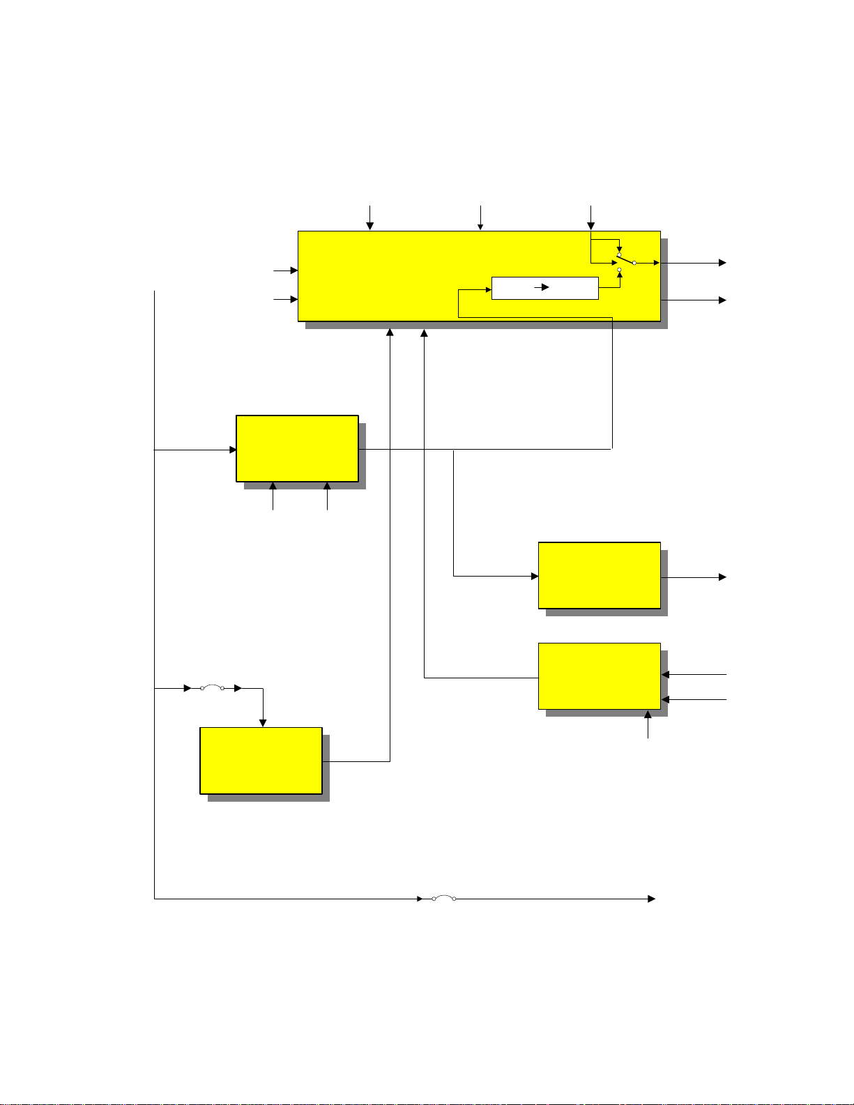
DP-85 DEFLECTION POWER SUPPLY SHUTDOWN
BLOCK DIAGRAM
IP01
ShutDown Pin (7)
on Power Supply
Driver &
Output IC
220V Short Det.
Heater
Short Det.
13V
Short Det.
28V Short Det.
Deflection B+ (130V)
Excessive Current Det.
IP06
Photocoupler
QP06
QP05
ShutDown
S.C.R.
DP25
Heater Too
High Det.
-M13V
Loss Det.
-M28V
Loss Det
Deflection B+ (130V)
Excessive Voltage Det.
DP23
DP34
X-RAY
PROTECT
Flyback
Excessive
Current Det.
Heater Loss
Det.
Excessive
High Voltage
Det.
Deflection
Transformer
Failure Det.
Side Pin
Failure Low
Det.
Q754
Side Pin
Failure High
Det.
High Voltage
Stability Too
High Det.
Page 02-05
Page 30
DP-85 DEFLECTION POWER SUPPLY SHUTDOWN DIAGRAM
TP91
DP11
13
CP16
IP01
ShutDown Pin (7)
on Power Supply
Driver &
Output IC
200V Short Det.
DP37
220V
Heater
DP36
DP35 ?
QP04
RP31
0.47
DP17
DP19
IP06
Photocoupler
Excessive High
Voltage Det.
DP35 May Not Be in Set.
Deflection B+ (130V)
Excessive Current Det.
DP18
DP23
QP05
ShutDown
S.C.R.
DP25
DP34
Deflection B+ 130V
Deflection B+ (130V)
Excessive Voltage Det.
Deflection Flyback
Excessive Current Det.
Flyback
TH01
9
QH03
10
DH24
5
DH31
QH07
DH30
RH23
1.2
Heater
DH25
DH26
DH27
Heater Loss Det.
Doesn't
go to
CRT's
DP30
13V
DP31
28V
DP27
DP26
RP45 RP44
-M28V
-28V Loss Det. -13V Loss Det.
+28V
Deflection B+ 130V V1
DP29
DP28
RP41 RP40
-M13V
Q777
QP06
13V Short Det.
28V Short Det.
+13V
6
1
DP33
DP32
Heater from Def. Power Supply. Goes
to CRT's
Heater To High Det.
7
8
T752
H.Blk
X-RAY
PROTECT
RP42
D759
C769
QH06
High Voltage Stability Too
D753
D757
Deflection Transformer
D754
Q754
D756
Inoperative Det.
High Det.
Side Pin Failure High
Det.
D760
Side Pin
Failure
Low Det.
Page 02-06
Page 31

13V
DP-85 CHASSIS L.E.D. (VISUAL TROUBLE DETECTION) DIODES
DEFLECTION PWB 5 GREEN L.E.D.s and 1 RED L.E.D.
(6 Total L.E.Ds. for visual trouble sensing observation)
130V
+28V
Deflection B+
RP39
-M28V-M13V
DP06 is a RED L.E.D.
Off = No IP01 B+
On (Mid) = IP01 B+
On (Bright) = Shutdown
Page 02-07
RP23
DP15
RP17
DP06
Osc B+
1.9V
RP37
ALL GREEN L.E.D.s
Start Up or Run
24.2V
5
IP01
Driver/Output IC
100% Dead Time &
7
IC B+ Detection
RP38
RP60
24.2V
1.9V
RP26
DP16DP22DP20
4
3
Vcc
IP06
IP06 Shutdown
Photocoupler
16 Shut Down
Inputs
RP46
DP21
1
2
QP05
Shutdown
SCR
Page 32

DP-85 DEFLECTION POWER SUPPLY DISTRIBUTION DIAGRAM
Page 02-08
Power Supply
Block
Protector
EP91: 4K
Switching
Control
IP01
DP06:
Protect
Red LED
Live Cold
Switching
Transformer
TP91
Feedback
IP05
Protect
IP06
Protector
EP92: 4K
Protector
EP93: 5K
Protector
EP94: 7K
Protector
EP95: 7K
Protector
EP96: 7K
Protector
EP97: 7K
Voltage Control
+130V: IP04
Rectifier
+220V:DP07
Rectifier
+7V:DP08
Rectifier
+15V:DP09
Rectifier
+15V:DP10
Rectifier
+28V:DP12
Rectifier
-28V:DP13
Rectifier
+130V:DP11
Regulator
+6.3V: IP02
Regulator
+13V: IP03
Regulator
-13V: QP01
Protector
EP96: 7K
Protector
SCR: QP05
DP36,
DP37:<4V
D
DP35: <4V DP32: >7.4V
D
DP15: +13V DP30: <5V
D
DP16: M-13V DP28: > -13V
D
DP20: +28V DP31: <5V
D
DP21: -28V
DP22: +130V QP04: >1.4V
Protect In
DP25: >-24V
D
D
Short
Circuit
Detector
On/Off
Over
Voltage
Detector
Power
ZD
DP28: >20V
ZD
DP26:
>32V
ZD
DP18:
>166
V
ZD
HVcc
Switch
QP08
Video
+220V
Heater
+6.3V
Vert/HVcc:
+13V
Vert:
-13V
Conver:
+28V
Conver:
-28V
Deflection
+130V
HVcc
+12V
DP-85 Deflection
Circuit Protection
Page 33

DM-1
Module
Power On/Off
by Remote or
Front Pannel
DP-85 DEFLECTION Vcc PRODUCTION CIRCUIT
PQD2
From I907 A12V Reg.
5
5
I001
Slave Micro
Power On/Off
Q007
53
Power ON
Driver
(Relay Driver)
A12V
PQS1
Other Power
On/Off Circuits
3
DEFLECTION PWBSUB POWER PWBSIGNAL PWB
A12V or STBY +12V
Start Up Power
QP08
23
3
I702
DVccVRef-In
I701
5V Reg.
I703
Comp.
1
1
2
DP41
1
PDD1
8
SUB DEFLECTION PWB
Run Power
RP66
13V
From IP03
13V Reg.
Page 02-09
Page 34

DP-85 SERIES CHASSIS HORIZONTAL DRIVE
CIRCUIT
Q701
PDD1
7
9
To I001 OSD
Position
To PinP
Unit
I702
H Out
18 16
29
FBP In
17
26
PSD2
6
H.Blk.
AVCC
Switched AVCC
Osc.
H. Sync In
Q751
Q755
To Convergence Circuit
To Sweep Loss Det. Circuit
C770
C771
IH01
Q1
A1
1
28V
12
T751
3
1
10
6
4
Osc
Q777
130V V1
IH02
Drive
H. Def. Yoke R
H. Def. Yoke G
H. Def. Yoke B
T752
1
6
QH08 QH01
7
8
H Pulse
11
12
9
10
QH09
Def.
+28V
+28P
M28V
M28P
7
To Side Pin Circuit
To Dynamic Focus
To Deflection Loss
To X-Ray Protect
130V V2
TH01
9
High
Voltage
10
Page 03-01
12
13
Clamp
E
QH10
14
1
Ref. V.
FBP In
QH05
QH04
HV Sample
12
QH06
HV Sample too High
X-Ray Protect
r
r
o
r
Page 35

DP-85 SERIES CHASSIS VIDEO SIGNAL PATH (Main & Terminal)
V1
Aux Inputs
V2
V3
4V
Avx 4 In
S-4 In
PinP TUNER (Mono)
S-1 In
S-2 In
Front Control PWB
DM-1
Digital Control Center
U001
Always PinP
S Det.
Aux Input 4
PMT1
Signal PWB
20
S Det.
S Det.
Terminal PWB
2
S-Y4
S-C4
Q202
PST1
3
S-Y1
S-C1
S-Y2
S-C2
PFV
8
5
3
I201
3
+
-
2
PinP Video
Terminal
PWB
1
20
21
23
5
3
7
9
11
13
15
17
50
Main Video
NTSC
I301
Yout1
Cout1
Lum/Audio
Selector IC
PinP V Out
36
44
42
Q035
Q301
3DY
Q302
3DC
Q039
PST1
11
13
Q034
6
C In
40
Y In
20
3
2
PMZ
I008
Y Out
I009
+
-
PCX
11
13
9
7
B-Y
Out
R-Y
Out
PST2
Comp/S-Y
S-C
3DY
3DC
Y1 In
29
B-Y1 In
30
R-Y1 In
31
21
22
1
PMS2
1
Q041
Q040
3DYC
Comb
Filter
I011
3
+
-
2
I010
3
+
-
2
U002
11
5
6
7
1
1
PinP V
Y
I
Q
PinP
Unit
Page 04-01
PZC
B
1
To CRT PWB
G
3
R
5
Signal Sub PWB
QX23
QX28
QX33
41
42
43
IX01
Rainforest
IC
53
51
52
Y
V/PR
U/PB
QX07
QX08
QX09
V/PR
U/PB
IX02
Y
1
QX01
3
+
-
2
Y
1
14
Y
DM1
IX03
1
1
QX03
3
+
-
2
QX05
3
+
-
2
V/PR
U/PB
3
5
PWB
ATSC/
NTSC
12
10
V (Cr)
U (Cb)
Page 36

DP-85 CHASSIS A.B.L. CIRCUIT DIAGRAM
See uP
Data
Signal
Path
PSZ2
RX78
RX79
QX14
RX80
9V
DX02
RX82
ABL
9
DX01
CX21
CX20
RX81
CX24
CX39
PSZ1
SDA2
16
SCL2
17 28
RH22
High Voltage B+
130V V2
QH03
See XRay Protect
RH23
CH18
Collector of Horz.
Output Transistor
Rainforest
45
27
SDA2
SCL2
To QH01
IX01
IC
B+
C
TH01
Signal Sub
PWB
To Anodes
To
Focus
ABL
3
Page 04-02
Signal
PWB
PSD2
1
ABL Pull-Up Resistors
Deflection PWB
Deflection B+ 130V
V1
[ Current Path ]
13V
RH59RH58
Clamp
As Brightness goes Up, ABL Voltage goes Down. (Inverse Proportional)
CH25
RH56
DH33
Page 37

DP-85 SWEEP & AC LOSS DETECTION CIRCUIT
12V
Vertical
Blanking
From
Pin 9 I601
V. Blk.
24V P/P
Horizontal
Blanking
From
Q755 Emitter
CN04
H. Blk.
11.6V P/P
SPOT
From Pin 9
of Micro I001
Cut Off
Vertical
Output IC
I601
Invert Input
Non Invert
Input
5V
CN01
R604
R605
QN01
RN01
RN02
CN03
QN05
RN11
RN12
PSD
2
2
3
Vert SAW
R602
5
4
Q601
Q602
Stops Vertical Drive
during Cut Off
adjustment, I2C
RN03
12V
RN10
RN09
DN04
DN05
Prevents CRT Burn
Q610
RN04
DN01
CN02
QN03
DN06
RN13
Spot Inhibit
QN07
RN06
8.57V
DN02
DN03
RN07
0V
RN08
DN11
RN16
RN15
CN05
DN07
9.72V
RN17
QN02
12V
8.57V
CN06
RN05
QN04
DN16
DN14
DN09
DN10
QN06
Horz. 13V Loss/
Start Up Spot Killer
QH02
14
1
13 Error Out
12
7
Stops High Voltage
Drive Signals From
being produced
during 13V start up
RN14
DN08
RN17
RH40
High Voltage
Driver IC
IH02
Reference
Feed Back
Error In
Drive
From I906 Pin 3
AC Photo Coupler
10V P/
P
ACK 5V
RN18
Page 04-03
Page 38

DP-85 SERIES CHASSIS AUDIO SIGNAL PATH
(Main, Terminal & Audio Output)
Page 05-01
4L
Avx 4 In
4R
NOTE: The J31101 Lum type connector Pins are
Aux Input 4
opposite of PMT1. They are correct here.
Front Control PWB
DM-1
Digital Control Center
I001
Microprocessor
Signal PWB 1 of 2
Surround PWB 2 of 2
Left Rear Spk Jack
Right Rear Spk Jack
External Right Spk Jack
External Left Spk Jack
Front Left Spk
Front Right Spk
PL
2
PR
2
Int.
Spk.
SS01
Center Spk
J31101
SCL1
47
SDA1
43
Ext.
Spk.
2
5
PMT1
7
4
PST3
5
4
PSP1
5
7
1
3
PCL
2
PFV
8
7
L-Audio (NTSC)
R-Audio (NTSC)
Terminal PWB
Rear Left
Rear Right
12
I401
FT/
Audio
Output
7
IC
Center
Terminal PWB
I202
3
+
-
2
5
+
-
6
2
4
11
12
1
7
SCL1
SDA1
Front Left
Front Right
I402
Center Audio
Output IC
20
22
Lum/Audio
Selector IC
6
Main Audio
4
27
26
Rear Output IC
12
I403
7
Q403
2
11
I301
Main Audio
PinP
Audio
Out
PinP
Audio
In
2
4
11
D414
D415
Q407
8
AVX 1
10
14
AVX 2
16
51
AVX 3
49
PST1
45
43
L
35
R
33
1
3
Audio Output PWB
D420
D421
Mute (PAS1 Pin 5)
D426
D427
Center Speaker Off
(PAS1 Pin 2)
Q411
Front Speaker Off (PAS1 Pin 1)
Mute (PAS1 Pin 5)
Left Total
10
Right Total
11
PinP Left
13
PinP Right
14
1
Mono PinP
Rear Speaker Off (PAS1 Pin 3)
Mute (PAS1 Pin 5)
Main Audio
Signal PWB
Left Select
Right Select
Signal PWB
2 of 2
20
PinP Tuner
Rear Left
Rear Right
F L Out
F R Out
LFE/SW
Sub Woofer
Center
1L
1R
2L
2R
3L
3R
PSU1
1
2
9
10
PAS2
8
9
1
2
4
6
Aux Inputs
(See Surround Audio Signal Path)
(See Surround Audio Signal Path)
Page 39

Right
Front
Left
Front
PAS2
2
1
DP85 SURROUND AUDIO SIGNAL
PATH
ISO1
Ft\
30
28
PinP Audio
PSU1
10
9
R
L
See Main Audio
Selector/Signal
PWB
Trans-
mitter
Audio
Cont
Rt
2
Selected Audio
Lt
1
Selected Audio
10
1
ISO8
Perfect
Volume
8
3
QS03 QS04
13
20
QS01 QS12
Transmitter
Out Jacks
FL/FR/RL/RR/PinP L/R
IG01
R
L
15
18
23
10
1
7
3
+
L Ft
-
2
R Ft
5
+
-
6
MAIN AUDIO
NOTE:
The connector Pins on
the DM-1 are backwards
compared to PMS1.
PMS1
R
1
1
3
L
1
3
2
3
2
IS10
+
-
IS09
+
-
Right
Total
In
Left
Total
In
MODULE
DM-1
To Audio Output PWB
Fixed/Vari
Audio Out L
Fixed/Vari
Audio Out R
Sub Woofer
LFE/
6
Sw
Center
4
To Audio Output PWB
R Ft + Center
L Ft + Center
Rear Right
Rear Left
QS13
LFE/Sw
IS12
1
7
Center
32
1
QS07QS08
QS09QS10
+
-
+
-
Center
3
2
5
6
13
CENT/LFE
20
15
18
Graphic EQ
ISO2
Mix/Vari
Audio
Cont.
R Ft
L Ft
R Ft
L Ft
5
3
1
32
1
IG15
Graphic EQ
LFE
(Sub Woofer)
Center
R Ft
L Ft
3
+
-
2
1
7
7
1
Center
IS07
IS05
LFE
(Sub
5
3
+
-
2
5
+
-
6
5
+
-
6
3
+
-
2
7
15
13
Woofer)
Center
R Ft
(Right
Front)
L Ft
(Left
Front)
MODULE
DM-1
9
10
Rear Right
Rear Left
5
6
3
2
IS04
+
-
+
-
7
1
2
3
6
5
IS06
IS11
+
-
+
-
Right
5
+
-
6
3
+
-
2
11
9
Rear
Left
Rear
PHP
1
7
1
3
To
Head
Phone
Jacks
R Ft +
7
1
Center
L Ft +
Center
Rear Right
Rear Left
32
1
15
18
ISO3
Rear/
Head-
Phone
Audio
Cont.
5
3
20
R R
L R
HPL
HPR
13
Page 05-02
Page 40

DP-85 Series Chassis AUDIO and VIDEO MUTE Circuit
Also see Mute Circuit Diagram (Surround and Audio Output PWB)
I001
V MUTE
Micro
Processor
MUTE
56
10
A5V
RO10
RO52
RO51
R145
D009
9V
A12V
RO93
Q022
RO92
D008
Mute 2
D010
R095
RO70
R094
Q008
PSD2
6
R096
R097
D011
C012
R098
V. Mute
"SPOT"
Horizontal & Vertical
Sweep Loss Det.
AC Loss Det.
(From Deflection PWB)
Q009
R099
Q010
V Mute 2
V Mute
Mute
2H Video PWB
From QZ13 and IZ07
HVBlk
PSZ2
Spot
14
DX05
PZC
7
PZC
7
Spot
Grounds Bias to Q8A3,
PSU1
16
V Mute 2
15
Mute 2
Rainforest
IX01
RY04
CRT PWBs
Q853 & Q803
Surround PWB
25
FBP
In
Page 05-03
Signal PWB
Page 41

DP-85 MUTE CIRCUIT DIAGRAM (SURROUND PWB)
Also see Audio and Video Mute Circuit Diagram
Also see Mute Circuit Diagram (Audio Output PWB)
VMUTE2
MUTE2
PSU1
16
15
Transmiter Right
DS20 DS21
Transmiter Left
DS22 DS23
Fixed/Variable Right
DS24 DS25
VMUTE2
Fixed/Variable
DS26 DS27
Left
QS05
RSC6
QS06
RSC7
QS11
RSF4
QS12
RSC4
RSC5
RSF2
RSF3
CS86RSH3CS73
CS87RSH4CS74
CS84RSH1CS77
CS85RSH2CS78
Transmiter Right
Out
Transmiter Left
Out
Fixed/Variable
Right Out
Fixed/Variable
Left Out
MUTE2
DS28
DS29
PSA1
VMUTE2
MUTE2 MUTE
4
5
VMUTE
LFE/Sub
Woofer
DS30
RSF5
QS14
RSF9
See Audio
Output Mute
Circuit
Diagram
RSF8
CS83CS82
LFE/Sub
Woofer Out
Page 05-04
Page 42

DP-85 MUTE CIRCUIT DIAGRAM (AUDIO OUTPUT PWB)
Also see Audio and Video Mute Circuit Diagram
Also see Mute Circuit Diagram (Surround PWB)
MUTE
Ft Spk Off
VMUTE 4
PAS1
5
1
D412
D413
D414
D415
D424
Front Right
Front Left
R418
C409
Rear Right
R415
Q401
R416
Q402
R417
Q403
Q409
R448
R412C401
R413C402
R444C440
R420
C403
R414
C404
R415
C442
R446
4
2
11
C409
4
Front
Right
Front Audio
Output IC
Front
Left
Mute
Rear
Right
Rear Audio
Output IC
I401
I403
Rear Spk
Off
Center
Spk Off
R413C402
Rear Left
C404
Rear
2
Left
Q410
3
D425
D426
D427
D418
R450
C447
Rear Left
R451
R449
Q411
R452
R431C423
Q406
2
D419
D420
D421
R436
C429
R437
R449
Q407
R438
R447
C425
R433
11
C448
2
11
C430
Mute
Center Audio Output IC
I402
Center
Center Audio
Output IC
Mute
Page 05-05
Page 43

DP-85 CHASSIS "DIGITAL CONVERGENCE" INTERCONNECTION CIRCUIT DIAGRAM
DM-1
2 4
9
5V
2
HMO1
IR Receiver
3
Ft. Control
Sensor
8 Total
Page 06-01
Sensors
PMF
1
QM05
PWB
PWB
LED
S0-S7
12
11
10
9
3
4
5
6
IR In
7
Out
QM01
I002
PMS2
IR
PFS
2
Memory
IP
IR
Out
I001
Main Up
19
23
17
21
57
Busy
44 Auto Conv. Sw.
Q002
PSD4
1
2
3
4
5
6
7
PDS1
+5V
1
N/C
2
Gnd
3
Gnd
4
S7
5
S6
6
S5
7
S4
8
S3
9
S2
10
S1
11
S0
12
OSD B
OSD G
OSD R
+5V
Deflection PWB
BUSY
OSD R
IR-In
OSDG
ADJ
OSDB
STAT
Adj B
42
Adj G
43
Adj R
54
OSD Blk
51
Busy 2
Signal PWB
SK01
"DCAM" Digital
Convergence Mode
QK0
6
QK0
7
QK0
8
5V Digital
Deflection PWB
Adj B
Dig OSD B
Adj G
Dig OSD G
Adj R
Dig OSD R
+5V SRAM
10
9
4
5
1
2
12
13
-5V
+5V
HBlk
D Size
V Sync
1 of 2 PDS
Gnd
S7
S6
S5
S4
S3
S2
S1
S0
B
I105
G
R
OSD Blk
1
PDG
2
3
4
5
6
7
8
9
10
11
12
13
14
15
UKDG
HC2111ASY
Convergence
"DCU"
"Mounted on
Deflection
1
2
3
4
5
6
7
8
9
10
11
D/H OSD Sel
BTX
8
GTX
6
RTX
3
OSD
11
Digital
Unit
PWB"
Q012
Q013
Q014
Q011
Blk
Signal PWB
PDS 2of 2
12
13
14
15
16
17
18
19
20
PSZ1
BV
BH
Gnd
GV
GH
Gnd
RV
RH
Mute
IK02
OSD B
13
OSD G
12
OSD R
11
OSD Blk
Normal
"Lo"
1
2
3
QX17
+27P
+33V
QX16
+28V
I501
33
Rainforest
34
QX15
35
3214
10
BV
5
15 16
IK05
BH
14
GH
6
817 12
817 12
GV
15 16
IK04
RV
14 13
RH
6 7
10 5
+27P +33V
Deflection PWB
PZC
QX33
QX28
5
B
To CRTs
3
G
41
42
QX23
43
1
R
To Blue Convergence Yokes
PCB
CYV+
CYVCYH+
CYH-
CYH+
CYH-
CYV-
CYV+
CYH+
CYH-
CYH-
2
1
4
3
PCG
4
To Green Convergence Yokes To Red Convergence Yokes
1
1
2
PCR
2
1
4
3
18
-
+
11
-
+
13
9
-
+
+
+
+
7
4
-33V-27P
4
18
-
11
-
CYH+
8
-
Page 44

DIGITAL CONVERGENCE OVERLAY AND MAGIC FOCUS
4 MODES TO DISPLAY A (4x3) IMAGE ON (16X9) DISPLAY
1
NORMAL MODE (4x3) FULL MODE (4x3)
Normal Mode 4X3 with Black Mask
DIGITAL CONVERGENCE ALIGNMENT
When performing a complete
Digital Convergence Alignment,
it is necessary to utilize an Overlay.
The 61HDX98B will require 2 (two)
different overlays.
One overlay will be utilized for any of the following:
1.) Normal mode
2.) Full mode
3.) Fill mode
(Liner)
3
FILL MODE (4x3)
2
Full Mode 4X3 Stretched to fit (Non-
Liner)
Cropped
And a different overlay will be utilized for:
4.) Smooth Wide Mode
After completion of Digital Convergence Alignment,
Memory Store must be performed. After Memory
Store, Sensor Initialization must be performed as
well.
Sensor Initialization must be performed after
the Digital Convergence alignment data is STORED
for any one of the following modes:
1.) Normal mode
2.) Full mode
3.) Fill mode
Also, Sensor Initialization must be performed after
the Digital Convergence alignment data is STORED
for the following
4.) Smooth Wide Mode mode
MAGIC FOCUS (AUTO DIGITAL CONVERGENCE)
Customer's function
When the customer presses the magic focus button,
it will be necessary for them to perform Magic Focus
in similar fashion.
Pressing Magic Focus will correct any one of the
following Modes:
1.) Normal mode
2.) Full mode
3.) Fill mode
Cropped
4
Fill Mode 4X3 Cropped
(Liner)
SMOOTH WIDE MODE
(4x3)
Liner
Liner
Magic Focus must also be pressed for:
4.) Smooth Wide Mode mode
Deflection Circuit remains at 23.75KHz for all modes, even HDTV 16X9. (Labeled in schematic as 2.14H)
Stretched Stretched
Smooth Wide Mode 4X3 Center (Liner) Outside edges Stretched to fit (Non-
Liner)
Page 06-02
Page 45

DIGITAL CONVERGENCE OVERLAY DIMENSIONS
20 88 113.4 2088113.4113.4113.4113.4113.4113.4113.4
41
49
97
97
DIGITAL CONVERGENCE OVERLAY FULL MODE
1350
H. SIZE
97
97
97
97
49
41
46.7
47.8
95.5
26 119 269511910710710710410411495
BR
762
Centering Offset
Part Number H312182A
V. SIZE
DIGITAL CONVERGENCE OVERLAY SMOOTH MODE
1350
H. SIZE
95.5
95.5
95.5
95.5
95.5
47.8
46.7
BR
762
Centering Offset
Part Number H312221
V. SIZE
Page 06-03
Page 46

DP85 SERIES CHASSIS "CLU-614MP" REMOTE CONTROL
REMOTE PERSONALITY WHILE IN THE
DIGITAL CONVERGENCE ADJUSTMENT MODE D.C.A.M.
To Clear R.A.M. data.
*
Turn set OFF.
Press and hold the Service Button on
deflection P.W.B. Then Power
Button.
POWER
D.C.A.M.
Digital convergence adjustment
mode
"PIP" = "ROM READ"
Reads old R.O.M. data.
(Last data stored in R.O.M.
(Press 2 times)
"PIP CH" = "INITIALIZE"
Perform after
STORE & before EXIT
[SWAP + PIP CH]
"ANT" = "PHASE"
*
(Aligns Cursor to Grid)
"INFO" = "CALCULATION"
(Calculates mid-points)
"MENU" = "REMOVE COLOR"
Removes color
not being adjusted.
(Will NOT remove GREEN )
"USER" ="GREEN adjust"
Digital Cursor Blinks GREEN
3x3 adjustment mode
*
(Press 5 times), can only be
entered when R.A.M. is cleared.
"MOVES DIGITAL CURSOR"
Moves Adjustment Point
(2) Up, (4) Left,
(5) Down, (6) Right
"INPUT" = "BLUE adjust"
Digital Cursor Blinks BLUE
13 x 9 adjustment mode
(Press 5 times)
TV SATCABLE
DTV/SAT
PIP CH M OVEANT
LAST
MUTE
VOL CH
INFO EXIT
GUIDE
USER HELP
MENU
FAV
CH
SVCS SCHED
REC SELECT
1
4
7
2
5
8
SWAPPIP
TV / CABLE / SAT
V C R
AUDIO
FAV
CH
3
6
9
C.S.INPUT
0
HITACHI
CLU-614MP
"SWAP" = "ROM WRITE"
(STORE)
Stores data into R.O.M..
(Press 2 times)
"MOVE" = "RASTER ADJ"
Used to align Red and Blue
raster with Green.
(2 Additional lines will Appear)
"EXIT" = "ENTER & EXIT"
Enter or Exit the D.C.A.M.
Must initially enter D.C.A.M. with
Service Button on chassis.
L
I
G
H
T
Toggles between External Video
and Internally generated Cross
hatch. After exiting the DCAM,
(Press 5X)
set can change channels or
external video source.
"CURSOR KEYS" =
"(ADJUSTMENT)"
Adjust the selected color at
the current stopping position.
Up
Down
Left
Right
" 0 " = "RED adjust"
Digital Cursor Blinks RED
7x5 adjustment mode
(Press 5 times)
PAGE 06-04
Page 47

DP-85 CHASSIS SLAVE MICROPROCESSOR I-001 PIN/PORT DESCRIPTION
Pin No. ID Port Identification Function Active
1 HSYNC OSD H. Pulse Receives Horizontal Blanking pulses 5VP/P for Service OSD positioning Pulse
2 VSYNC OSD V.Pulse Receives Vertical Blanking pulses 5VP/P for Service OSD positioning Pulse
3 AD4 AFC Receives the AFC S-Curve signal produced by the PinP tuner indicating the accuracy of the PinP tuning. Signal
5 TIM2 PIP Sync Det Detection of PinP Tuner Sync for Auto Programming and AFC Low
6 P43 AC (50/60 Hz) Detection of A/C line frequency from Schmitt Amp Q015 and Q016 Pulse
7 AD3 Side Panel APL Timing Pulse input for OSD creation of Side Panels Pulse
8 AD2 Dimmer (Not Used) n/a
9 P26 V.STOP Cutoff. This output Stops the Vertical circuit and shuts off the Spot circuit High
10 P27 CH Change Mute Mutes Audio through Q022 to Surround PWB during channel change High
11 PWM4 H.BLK-HP Outputs a control signal to the RC network attached to IZ06 controlling the phase of the Side Pannel pulses. High
12 P50 MAIN/PinP Outputs a control signal to I012 for selection of Main Sync or PinP Sync. High
13 P01 SCL Clock for the EEPROM Data
14 P47 Smooth Wide Outputs control signal to Q753 and I751 to switch deflection to Smooth Wide High
15 P02 SDA Data for the EEPROM Data
16 P51 4:3 When Fill, Full or Smooth Wide mode is selected in NTSC, output high to prevent generation of Mask Pulse
17 SIN Tx Data output from Slave Micro to DM-1 module Data
18 N/A N/A No Connection
19 INT1 Request Request data from/to the DM-1 Module Data
20 N/A N/A No Connection
21 SOUT Rx Data input from DM-1 module to Slave Micro Data
22 N/A N/A No Connection
23 SCLK Clock Clock for the DM-1 data transmission Data
24 Avcc Avcc +5V
25 HLF HLF
26 RVCO TRVCO Resistive Fixed
27 VHOLD VHOLD Fixed by Capacitor
28 CVIN C. Video Input Input for Composite Video for Closed Caption detection. However, the DM-1 module actually generates the Closed Caption charac-
29 CNVSS CNVSS
30 OSC In OSC in
31 OSC Out OSC Out
32 VSS Ground Ground
33 Vcc Vcc +5V
34 OSC In OSC In
Page 07-01
35 OSC Out OSC Out
since no side panels are used.
ters.
High
Signal
Page 48

DP-85 CHASSIS SLAVE MICROPROCESSOR I-001 PIN/PORT DESCRIPTION
Pin No. ID Port Identification Function Active
36 CVIN Reset Reset active Low. Reset by I003 during first AC power application and by Q026 when the DM-1 module resets the Slave Microproc-
37 P31 CLOCK Clock for the PinP Tuner data communications Data
38 P30 DATA Data for the PinP Tuner for Channel change, Programmable Divider, band selection, etc.. Data
39 P03 ENABLE Enables the reception of data by the PinP Tuner Data
40 P16 Headphone SEL Det Active Low detects the insertion of the Headphone Jack Low
41 P15 LOCK Notifies the Slave Micro by a Low, when the PinP tuner PLL Phase Detector is locked Low
42 SDA2 SDA Data for controlling the 1H Video, 2.14 Video Processor, PinP, LFE/Center Audio Control, Headphone/Rear Audio Control, 3DYC
43 SDA1 SDA Data for the PinP/Front audio controller and AV switch IC Data
44 P67 Auto
Convergence SW
45 SCL2 SCL Clock for controlling the 1H Video/Chroma, 2.14 Video Processor, PinP, LFE/Center Audio Control, Headphone/Rear Audio Control,
46 P66 P.BLK. (Not Used) n/a
47 SCL1 SCL Clock for the PinP/Front audio controller and AV switch IC Data
48 P65 Data Data to control the Front L/R and Center Graphic Equalizer Data
49 P10 KEYIN Not Used. n/a
50 P20 KEYIN Notification of the OEM in which the chassis is used. Diode D002 identifies it as Hitachi by feeding back Key Out2 pulses from pin
53 P20 Power ON/OFF When the DM-1 Module instructs the Slave Micro. to turn ON, this output goes high High
54 P62 Clock Clock for data communications to control the Front L/R and Center Graphic Equalizer Data
55 P07 Auto Convergence Size When Magic Focus is initialized or run, the deflection size is widened to guarantee light strikes the Photo cells. High
56 P61 V.MUTE Mutes Audio and Video through Q008 and Q010 to Sub Video and Surround PWB during channel change High
57 P06 Auto
Convergence Busy
58 P60 UV/IQ Not Used. n/a
59 P05 HOR. Det Receives a High when the 130V line is drawing excessive current. Shuts off relay. High
60 P04 Run Supply Det. (Not Used) n/a
61 OSC Blk OSD (Blk) Outputs a pulse slight wider and in time with the OSD characters to clean up video where character will be displayed. Pulse
62 B OSD (B) Outputs Blue characters for the Service Menu Pulse
63 G OSD (G) Outputs Green characters for the Service Menu Pulse
64 R OSD (R) Outputs Red characters for the Service Menu Pulse
essor.
and Deflection IC's.
When the Magic Focus switch is pressed, the DM-1 module notifies the Slave Micro.
Then the Slave Micro outputs a high from this pin to the DCU to start Magic Focus.
3DYC and Deflection IC's.
38.
Whe the DCU is activated by the Service Only switch, this pin is notified via Q002. After notification,
the Slave Microprocessor notifies the DM-1 module via data to ignore Infrared commands.
Low
Data
High
Data
Data
High
Page 07-02
Page 49

DP-85 SYSTEM CONTROL PORT DESCRIPTION
U001
AC (50/60 Hz)
PIP Sync Det
Side Panel APL
(N/A) Dimmer
CH Change Mute
Smooth Wide
H.BLK-HP
Arm Up
DM-1
Rx SOUT
Auto Convergence SW P67
Power On/Off P20
V.MUTE P61
V.STOP P26
(N/A) P.BLK P66
Headphne SEL Det P16
HOR. Det P05
(N/A) Run Supply Det
Auto Convergence Busy
Auto Convergence Size
OSD (Blk)
6
P43
TIM2
AD3
AD2
P27
P47
7
8
10
14
PWM4
INT1Request
19
SCLKClock
17
SINTx
44
53
56
9
46
40
59
60
P04
57
P06
55
P07
OSC Blk
49
47
43
45
42
37
38
39
41
3
50
13
15
SCL1
SDA1
SCL2
SDA2
AD4
P10/
I001
5
11
23
21
130V Ex. Current
61
P31
P30
P03
P15
P23
P01
P02
CLOCK
DATA
ENABLE
LOCK
AFC
KEYIN
SCL
SDA
SCL
SDA
SCL
SDA
SCL
SDA
SCL
SDA
SCL
SDA
SCL
SDA
SCL
SDA
I002
IS01
I008
IX01
U002
I301
IS02
IS03
PINP
TUNER
EEPROM
PINP/Front
Audio Control
1H Video/
Chroma
2.14H Video
Processor
PinP
AV SW
LFE/Center
Audio Control
Headphone/Rear
Audio Control
OSD (B)
OSD (G)
OSD (R)
OSD H.Pulse
OSD V.Pulse
(N/A) UV/IQ
4:3
MAIN/PinP
C. Video Input
62
B
63
G
64
R
HSYNC
VSYNC
58
P60
16
P51
12
P50
CVIN
28
SCL
U301
3D Y/C
SDA
SCL
I702
Deflection
SDA
1
IG02
2
48
54
P65
P62
Data
Clock
Front L/R
Graphic
Equalizer
IG11
Data
Center
Graphic
36
Clock
ResetCVIN
Equalizer
Page 07-03
Page 50

DP-85 CHASSIS MICROPROCESSOR DATA COMMUNICATIONS CIRCUIT DIAGRAM
IOO1
Micro Processor
SCL2
SDA2
NOTE:
J22600 Lum type connector
Pins on the DM-1 are
backwards compared to
PMS2.
ICP TX
ICP REQUEST
ICP RX
ICPCLK
SDA3
SCL3
45
42
17
19
21
23
15
13
PMS2
5
3
6
4
10
12
9
11
5
6
U002
2
1
PCX
3
2
J22600
SDA3
SCL3
SDA2
SCL2
SCL2
SDA2
PinP
UNIT
3D Y/C
UNIT
DM-1
MODULE
IOO2
EEPROM
SDA2
I008
1H Video/
Chroma
3334
SCL2
PSZ1
17
16
PSU1
4
5
PSD1
1
2
26
27
PDD2
9
8
2H Video PWB
SCL2
SDA2
IX01
Rainforest
SCL2
SDA2
Sub Deflection PWB
I702
Sweep Control
SCL2
4
SDA2
3
Surround PWB
16
Center/LFE
17
Audio Control
16
Rear/Headphone
17
Audio Control
IS02
IS03
Page 07-04
GEQ CLOCK
GEQ DATA 13
PinP Tuner Enable
PinP Tuner Data
PinP Tuner Clock
SDA1
54
48
39
38
37
43SCL1
47
17
Enable
16
Data
15 Clock
U001
Tuner 2
(Mono)
Pinp
12
GEQ CLOCK
GEQ DATA
27
26
SCL1
SDA1
6
7
IS01
Front/Transmit
Audio Control
16
17
16
17
Terminal PWB
IG02
Front
Equalizer
IG11
Center
Equalizer
I301
PST3
5
4
27
26
SDA1
A/V Select
SCL1
Page 51

DP-85 SERVICE ADJUSTMENT ORDER “PREHEAT BEFORE BEGINNING”
Order Adjustment Item Screen Format Signal DCU Data
1
Cut Off FULL
2
Pre Focus FULL
3
DCU Phase Data Setting FULL
4
DCU Phase Data Setting SMOOTH
5
Horz. Position Adj. (Coarse) FULL
6
Horz. Position Adj. (Coarse) SMOOTH
7
Raster Tilt FULL
8
Beam Alignment FULL
9
Raster Position FULL
10
Horz. Blanking Phase FULL
11
Horz. Size Adjust FULL
12
Vertical Size Adjust FULL
13
Trapezoid FULL
14
Side Pin FULL
NTSC
NTSC
NTSC
NTSC
NTSC
NTSC
NTSC
CLEAR
NTSC
NTSC
CLEAR
NTSC
NTSC
NTSC
NTSC
NTSC
CLEAR
CLEAR
CLEAR
CLEAR
15
Horz. Size Adj. SMOOTH
16
Vertical Size Adjust SMOOTH
17
Trapezoid SMOOTH
18
Side Pin SMOOTH
19
Beam Form NORMAL
20
Lens Focus Adjust FULL
21
Static Focus Adjust FULL
22
Blue Defocus FULL
23
White Balance Adjustment FULL
24
Sub Brightness Adjustment FULL
25
Horz. Position Adjustment FULL
26
Horz. Position Adjustment SMOOTH
27
Convergence Alignment FULL
28
Convergence Alignment SMOOTH
29
Magic Focus Initialize FULL
30
Magic Focus Initialize SMOOTH
NTSC
NTSC
NTSC DCU Grid
NTSC
NTSC
NTSC
NTSC
NTSC
NTSC
NTSC Color Bar
NTSC
NTSC
NTSC
NTSC
NTSC
NTSC
CLEAR
CLEAR
CLEAR
CLEAR
CLEAR to start
It is necessary to follow the order when performing an alignment on the 61HDX98B
PAGE 08-0 1
Page 52

DP-85 I2C SERVICE MODE Page 1 of 4 Total of 117 Adj. with 13 Field Adjustments
OSD
(Text)
ADJ.
RANGE
INIT.
VALUE
CONTROLLED
DEVICE
YES
YES
YES
YES
YES
YES
YES
YES
YES
YES
YES
YES
YES
No.
1 SERVIC SERVICE Off/On Off
2 SUBBRT SUB BRIGHTNESS 0~255 127
3 HBLKPH
4 HPOS-F H. Position (Full) 0~127 76
5 SPIN Side Pin (Full) 0~63 22
6 TRAP Trapezoid (Full) 0~63 25
7 HSIZ H. Size (Full) 0~127 30
8 VSIZ-F V. Size (Full) 0~127 46
9 H-POS-S H. Position (Smooth) 0~127 76
10 SPIN-S Side Pin (Smooth) 0~63 18
11 TRAP-S Trapezoid (Smooth) 0~63 26
12 HSIZ-S H. Size (Smooth) 0~127 58
13 VSIZ-S V. Size (Smooth) 0~127 47
14 PHPOSI PIP H. Position (CENTER) 0~63 14 PinP Unit
15 PVPOSI PIP V. Position (CENTER) 0~63 12 PinP Unit
16 CONT Contrast (CENTER) 0~127 63 UNI-COLOR -18dB to 0dB TA1276AN
17 CONT-T Contrast (Center offset) Theater Mode 0~127 63 UNI-COLOR -18dB to 0dB TA1276AN
18 BRT-YIQ Brightness YIQ TA1276AN
19 BRT-T Black Level (Center offset) Theater Mode 0~255 127 -40IRE to +40IRE TA1276AN
20 C-YIQ Color (Center) (NTSC-YIQ) 0~127 63 Color Min -20dB to +4dB TA1276AN
21 C-170 Color (Center) (SMPTE-170M) 0~127 63 TA1276AN
22 C-709 Color (Center) (ITU-R709) 0~127 63 TA1276AN
23 T-YIQ Tint (Center) (NTSC-YIQ) 0~127 63 TINT -32deg to +32deg TA1276AN
24 T-170 Tint (Center) (SMPTE-170M) 0~127 63 TA1276AN
25 T-709 Tint (Center) (ITU-R709) 0~127 63 TA1276AN
26 S-NTSC Sharpness (Center) (NTSC) 0~127 63 Sharpness Min -20dB to +14dB TA1276AN
27 S-SDTV Sharpness (Center) (SDTV) 0~127 18 TA1276AN
28 S-HDTV Sharpness (Center) (HDTV) 0~127 63 TA1276AN
29 S-T Sharpness (Center offset) Theater Mode 0~127 63 SHARPNESS -20dB to +14dB TA1276AN
30 G-9300 Green Drive (9300K) 0~127 63 DRIVE -5dB to 0dB to +3dB TA1276AN
H. BLK. PHASE
ADJUSTMENT ITEMS
0~63 32
ADJ. VARIABLE RANGE
-40IRE to +40IRE TA1276AN
uPc1885
uPc1885
uPc1885
uPc1885
uPc1885
uPc1885
uPc1885
uPc1885
uPc1885
uPc1885
Only adjust those adjustments with a YES in the ADJ column.
Page 08-02
Page 53

DP-85 I2C SERVICE MODE Page 2 of 4 Total of 117 Adj. with 13 Field Adjustments
OSD
(Text)
ADJ.
RANGE
INIT.
VALUE
CONTROLLED
DEVICE
No.
ADJUSTMENT ITEMS
ADJ. VARIABLE RANGE
31 B-9300 Blue Drive (9300K) 0~127 63 TA1276AN
32 G-7500 Green Drive (7500K) 0~127 54 TA1276AN
33 B-7500 Blue Drive (7500K) 0~127 46 TA1276AN
34 R-CUT Red Cutoff 0~255 127 R CUTOFF 2V to 2.5V to 3V TA1276AN
35 G-CUT Green Cutoff 0~255 127 G CUTOFF 2V to 2.5V to 3V TA1276AN
36 B-CUT Blue Cutoff 0~255 127 B CUTOFF 2V to 2.5V to 3V TA1276AN
37 HFVM H. F/V Min. OSC Frequency (Full) 0~63 8 uPc1885
38 HFVO H. F/V OSC Frequency (Full) 0~63 31 uPc1885
39 SPB-F Side Pin Balance (Full) 0~31 15
40 HDTY-F H. Duty (Full) 0~31 15
uPc1885
uPc1885
41 SPC Side Pin Corner (Full) 0~63 31 uPc1885
42 ----- Don't Care
43 VSL-F V.S. Linearity (Full) 0~31 15 uPc1885
44 VCL-F V.C. Linearity (Full) 0~31 15 uPc1885
45 ----- Don't Care
46 ----- Don't Care
47 ----- Don't Care
48 RGBBRT RGB Black Level (Digital Convergence) 0~127 63 -4dB to 0dB to +3dB TA1276AN
49 RGBCNT RGB Contrast (Digital Convergence) 0~127 90 -18dB to 0dB TA1276AN
50 WPSL White Peak Suppressing Level (WPSL) 0~1 1 0:130IRE 1:110IRE TA1276AN
51 HIBRT High Bright Color (HIBRT) 0~1 0
52 CGAMMA Color Gamma Correction Point 0~3 0
53 CLIMIT Color Limiter Level (CLR) 0~1 0
54 SUBCNT Sub Contrast 0~31 16
55 YGAMMA Y-Gamma CURVE 0~3 0
56 CDE CDE 0~1 1
57 RPHYIQ (R-Y) Phase (NTSC-YIQ) 0~3 2
58 RBGYIQ (R-Y) / (B-Y) Gain (NTSC-YIQ) 0~3 0
59 GPHYIQ (G-Y) Phase (NTSC-YIQ) 0~3 2
60 GBGYIQ (G-Y) / (B-Y) Gain (NTSC-YIQ) 0~3 0
0:Off 1:On
0:Off 1:O.2Vp-p 2:0.4Vp-p 3:0.6vp-p
0: 1.8Vp-p 1: 2.2Vp-p
-3dB to +3dB
0:Off 1:-2.5dB 2:-4.8dB 3:-6.5dB
0:On 1:Off
0:90deg 1:92deg 2:94deg 3:112deg
0:0.56 1:0.68 2:0.79 3:0.86
0:236deg 1:240deg 2:244deg 3:253deg
0:0.30 1:0.34 2:0.40 3:0.45
TA1276AN
TA1276AN
TA1276AN
TA1276AN
TA1276AN
TA1276AN
TA1276AN
TA1276AN
Only adjust those adjustments with a YES in the ADJ column.
Page 08-03
Page 54

DP-85 I2C SERVICE MODE Page 3 of 4 Total of 117 Adj. with 13 Field Adjustments
OSD
(Text)
ADJ.
RANGE
INIT.
VALUE
CONTROLLED
DEVICE
No.
61 RPH170 (G-Y) Phase (SMPTE-170M) 0~3 0
62 RBG170 (R-Y) / (B-Y) Gain (SMPTE-170M) 0~3 2
63 GPH170 (G-Y) Phase (SMPTE-170M) 0~3 2
64 GBG170 (G-Y) / (B-Y) Gain (SMPTE-170M) 0~3 3
65 RPH709 (R-Y) Phase (ITU-R709) 0~3 0
66 RBG709 (R-Y) / (B-Y) Gain (ITU-R709) 0~3 3
67 GPH709 (G-Y) Phase (ITU-R709) 0~3 2
68 GBG709 (G-Y) / (B-Y) Gain (ITU-R709) 0~3 0
69 OSDACL OSD-ACL (OS-ACL) 0~1 1
70 RGBACL RGB-ACL (TX-ACL) 0~1 0
71 SVM-PH VSM PHASE 0~3 3
ADJUSTMENT ITEMS
ADJ. VARIABLE RANGE
0:90deg 1:92deg 2:94deg 3:112deg
0:0.56 1:0.68 2:0.79 3:0.86
0:236deg 1:240deg 2:244deg 3:253deg
0:0.30 1:0.34 2:0.40 3:0.45
0:90deg 1:92deg 2:94deg 3:112deg
0:0.56 1:0.68 2:0.79 3:0.86
0:236deg 1:240deg 2:244deg 3:253deg
0:0.30 1:0.34 2:0.40 3:0.45
0:On 1:Off
0:Gain1/2 2:Normal
0:-40ns 1:-20ns 2:0ns 3:+20ns
TA1276AN
TA1276AN
TA1276AN
TA1276AN
TA1276AN
TA1276AN
TA1276AN
TA1276AN
TA1276AN
TA1276AN
TA1276AN
72 PIPVOL PinP Volume
73 APC-NT APACON PEAK f0 (NTSC) 0~7 7
74 APC-SD APACON PEAK f0 (SDTV) 0~7 6
0:Off 1:4MHz 2:3.3MHz 4:2.5MHz
5:Off 6:13MHz 7:10MHz 8:8MHz
TA1276AN
TA1276AN
75 APC-HD APACON PEAK f0 (HDTV) 0~7 5 TA1276AN
76 SVMLMT Velocity Modulation Limit 0~1 0
77 DCR-PO D.C. Restoration Point 0~7 0
78 DCR-RA D.C. Restoration Rate 0~7 0
79 DCR-LI D.C. Restoration Limit 0~3 0
80 BSP
81 ABSP
82 BSP-T
83 ABSP-T
84 YGM-PO
85 STRCNT
86 STRCSD
Black Stretch Start Point
APL to Black Stretch Start Point
Black Stretch Start Point (Theater)
APL to Black Stretch Start Point (Theater)
Y-Gamma Point
0~7 2
0~3 1
0~7 0
0~3 0
0~1 0
0:Parabola Modulation OFF 1:On
0:0% to 7:42%
0:100% to 7:130%
0:100% 1:87% 2:73% 3:60%
0:22IRE to 7.56IRE
0:0dB to 3:1.5dB
0:22IRE to 7.56IRE
0:0dB to 3:1.5dB
0:100IRE 1:95IRE
TA1276AN
TA1276AN
TA1276AN
TA1276AN
TA1276AN
TA1276AN
TA1276AN
TA1276AN
TA1276AN
87 STRCHD
88 RGB-GM
89 BLC
90 BSG
RGB-Gamma
Black Level Automatic Correction (B.L.C.)
Black Stretch Gain (B.S.G.)
0~1 1
0~1 1
0~1 1
0:OFF 1:ON
0:OFF 1:ON
0:ON 1:OFF
TA1276AN
TA1276AN
TA1276AN
Only adjust those adjustments with a YES in the ADJ column.
Page 08-04
Page 55

DP-85 I2C SERVICE MODE Page 4 of 4 Total of 117 Adj. with 13 Field Adjustments
OSD
(Text)
ADJ.
RANGE
INIT.
VALUE
CONTROLLED
DEVICE
No.
91 BDL
92 DADV
93 DAS
94 ABLV
95 ABLS
96 ABLV-T
97 ABLS-T
98 TINT-P
99 CLR-P
100 TNT-NT
101 CNT-NT
102 CLR-NT
103 CCD-D
104 CCD-S
105 CCD-W
106 CCD-C
107 CCD-SD
108 CCD-CD
Black Detection Level (B.D.L.)
Dynamic ABL Detection Voltage
Dynamic ABL Sensitivity
ABL Detection Voltage
ABL Sensitivity
ABL Detection Voltage (Theater)
ABL Sensitivity (Theater)
Tint (PinP)
Color (PinP)
Tint (Main Picture) NTSC
Contrast (Main Picture) NTSC
Color (Main Picture) NTSC
CCD Data Slice Line (00E0H)
CCD Start Bit Position (00E1H)
CCD Window Position (00E2)
CCD Clock Line Counter (00E6H)
CCD Start Bit Position (00E7H)
CCD Clock Line Detection (00E9H)
ADJUSTMENT ITEMS
ADJ. VARIABLE RANGE
0~1 1
0~7 0
0~7 0
0~7 0
0~7 0
0~7 0
0~7 0
0:3IRE to 1:0IRE
0:MIN 7:MAX
0:MIN 7:MAX
0:MIN 7:MAX
0:MIN 7:MAX
0:MIN 7:MAX
0:MIN 7:MAX
TA1276AN
TA1276AN
TA1276AN
TA1276AN
TA1276AN
TA1276AN
TA1276AN
0~255 160 PinP Unit
0~255 121 PinP Unit
0~127 56 TA1270AF
0~31 27 TA1270AF
0~31 12 TA1270AF
0~255 17
0~255 210
0~255 41
0~255 5
0~255 1
0~255 108
109 YNR
110 YOUTGM
111 ----- Don't Care
112 RESET
Initial Set
113 ----- Don't Care
114 HFV H. F/V (Full) 0~255 243 uPc1885
115 VPOS-F V. Position (Full) 0~127 63 uPc1885
116 VMAX-F V. Output Max. Size (Full) 0~31 18 uPc1885
117 VSM-GA VSM GAIN 0~3 0
0:0dB 1:-6dB 2:-9dB 3:Off
TA1276AN
Only adjust those adjustments with a YES in the ADJ column.
Page 08-05
Page 56

DP-85 SERIES CHASSIS MAGNETS, SCREEN CONTROLS and FOCUS BLOCK ASSEMBLY
DP-85 MAGNETS
Adjustment Points
FRONT
RED CRT GREEN CRT BLUE CRT
4
5
(1)
Centering magnet RED
(2)
Centering magnet GREEN
(3)
Centering magnet BLUE
(4)
Beam Form Magnets
21 3
4
6
5
(5)
Beam Alignment magnets
(6)
Focus Block Assembly RED, GREEN &
4
5
BLUE
Also: Drive Adjustment controls for
RED, GREEN & BLUE
PAGE 08-0 6
Page 57

PRE HEAT RUN CONDITION DP-85 Series Chassis.
PRESET EACH ADJUSTMENT
VR TO CONDITION AS
SHOWN:
A) Before Pre Heat Run.
1) Red and Green Drive VR on
the CRT PWB. (Not on Blue
CRT).
Pre set
12~2
between the
12 o’clock
and 2 o’clock
position.
DRIVE VR
2) SCREEN VR ON FOCUS
PACK.
Pre Set fully counter
clockwise.
SCREEN VR
3) Focus VR on focus pack
Pre Set fully clockwise.
FOCUS VR
Projection Front View
RED CRT GREEN CRT BLUE CRT
Screen VR
R G B
Focus VR
R G B
FOCUS PACK
PAGE 08-0 7
Page 58

CUT OFF and FOCUS ADJUSTMENT DP-85 CHASSIS
ADJUSTMENT PREPARATION:
A) Pre Heat Run should be
finished.
ADJUSTMENT PROCEDURE:
1) Go to I
2
C ADJ. Mode. (With
power ON, press the TV/
SAT and the CURSOR
DOWN [q] button. The
Service Menu is displayed.)
2) Choose SERVICE item [1]
of I2C ADJ. Mode. (Select
CURSOR RIGHT [u] and
the Vertical will collapses).
3) Adjust any Screen VR.
Screen VR should be turned
clockwise gradually until
that particular color is
barely visible.
4) Repeat for the other two
colors.
FOCUS ADJUSTMENT:
1) Short the 2pin subminiature connector on the
CRT PWB (TS), to remove
any color not being
adjusted and adjust one
color at a time. (The
adjustment order of R, G
and B is just an example.)
2) Adjust the Focus VR for
Red until maximum Focus is
achieved.
3) Repeat for Blue and Green.
4) To Return to Service Menu,
press the CURSOR RIGHT
[u] key on remote.
Screen VRs
Focus VRs
Projection Front View
RED CRT GREEN CRT BLUE CRT
Screen VR
R G B
Focus VR
R G B
FOCUS PACK
PAGE 08-0 8
Page 59

DP-85 CHASSIS
DCU CROSS-HATCH PHASE SETTING ADJUSTMENT PROCEDURE
Adjustment Preparation:
1) Cut Off adjustment should
be finished.
2) Video Control: Brightness
90%, Contrast Max.
Adjustment Procedure:
1) Receive any NTSC signal.
2) Screen Format is FULL
3) Press and Hold the
SERVICE ONLY switch on
the deflection PWB.
4) Press the ANT key on the
Remote, then press the
EXIT key. (This is the
Phase adjustment mode).
5) Adjust data value using the
keys indicated in the chart,
until the data matches the
values indicated in the
chart.
Exiting Adjustment Mode:
6) Press Help key on remote
control.
7) Press SWAP key TWICE to
store the information.
8) When Green dots are
displayed, press the 8 key
on remote.
9) Press the SERVICE ONLY
switch to return to normal
mode.
SMOOTH Mode Adjustment
Mode:
10) Change the Display Format
to SMOOTH/WIDE Mode.
11) Repeat steps 3 through 9
for the SMOOTH/WIDE
mode.
PHASE MODE (FULL and SMOOTH/WIDE)
Display Format
ADJUST USING
4 and 6 keys on Remote
2 and 5 keys on Remote
Cursor Left t and Right u on Remote
Cursor Up p and Down q on Remote
Address Data Value
PH-H B9
PH-V 07
CR-H 4E
CR-V 0C
PAGE 08-0 9
Page 60

DP-85 CHASSIS
HORIZONTAL POSITION “COARSE” ADJUSTMENT PROCEDURE
Adjustment Preparation:
1) Cut Off adjustment
should be finished.
2) Video Control: Brightness 90%, Contrast
Max.
Adjustment Procedure
NORMAL MODE:
1) Receive any NTSC
crosshair signal.
2) Screen Format is NOR-
MAL
3) Press the SERVICE
ONLY switch on the
deflection PWB and
display the Digital Convergence Crosshatch
pattern.
4) Mark the center of the
Digital Convergence
Crosshatch Pattern
with finger and press
the SERVICE ONLY
switch to return to
normal mode.
5) Enter the I2C Bus alignment menu and select
Item [4] HPOS-F and
adjust the data so that
the center of Video
matches the location
of the Digital Crosshatch pattern noted in
step {4}.
6) Write down the data
value.
7) Exit from the I2C
Menu.
SMOOTH/WIDE Mode
Adjustment:
1) Receive any NTSC
crosshair signal.
2) Screen Format is
SMOOTH.
3) Press the SERVICE
ONLY switch on the
deflection PWB and
display the Digital Convergence Crosshatch
pattern.
4) Mark the center of the
Digital Convergence
Crosshatch Pattern
with finger and press
the SERVICE ONLY
switch to return to
normal mode.
5) Enter the I2C Bus alignment menu and select
Item [9] HPOS-S and
adjust the data to the
same value as the data
value entered for the
NORMAL mode Step
{6}.
6) Press the MENU button
on remote to exit service menu mode.
PAGE 08-10
Page 61

DP-85 CHASSIS
RASTER TILT (Deflection Yoke) ADJUSTMENT PROCEDURE
Adjustment Preparation:
1) The set can face any
direction.
2) Receive the CrossHatch Signal
3) VIDEO CONTROLS:
Factory Preset.
4) SCREEN FORMAT:
should be FULL mode.
5) The lens focus should
have been coarse adjusted.
6) The electrical focus
should have been
coarse adjusted.
7) The Digital Convergence RAM should be
cleared.
(Turn power off, press
and hold the SERVICE
ONLY switch, then
press the POWER button).
The Service Only
switch is on the Deflection PWB.
Adjustment Procedure :
GREEN:
1) Apply covers to the
RED and BLUE lenses
or short the 2P Sub
Mini connector [TS] on
each CRT PWB to produce only GREEN.
2) Turn the Green defle ction yoke and adjust
the TILT until the
green is level. [+/-
2mm tolerance]. See
diagram.
RED:
1) Remove cover from
RED CRT and align
RED with GREEN.
2) [+/- 1mm tolerance
when compared to
Green]
BLUE:
1) Remove cover from
BLUE and cover the
RED CRT. Align BLUE
with GREEN.
2) [+/- 1mm tolerance
when compared to
Green]
3) REMOVE ALL COVERS.
4) Turn the power off.
l = ñ 2mm
l
Vertical Center axis of
Cross-Hair signal
PAGE 08-11
Page 62

BEAM ALIGNMENT for DP-85 CHASSIS
ADJUSTMENT
(WARNING: Remove all rings, watches and jewelry to avoid shock.)
Preparation for adjustment:
1) Adjust at least 30 minutes
after turning on power
switch.
2) Raster inclination, centering, horizontal and vertical
amplitudes and optical focus adjustment should be
completed.
3) Brightness: 90%
Contrast Max.
4) Receive cross hatch signals,
or dot pattern
RASTER TILT adjustment
should be finished.
5) SCREEN FORMAT should
be FULL mode.
Adjustment procedure:
1) Green (G) tube beam alignment adjustment:
Short-circuit 2P subminiature connector plug pins of
Red (R) and Blue (B) on the
CRT boards and project
only Green (G).
2) Put Green (G) tube beam
alignment magnet to the
cancel state as shown in
Figure 1.
Fig. 1
The figure shows that the
long and short knobs of the
2P magnet are aligned, this is
the cancel state.
3) Turn the Green (G) static
focus VR counterclockwise
all the way and make sure
of position of cross hatch
center on screen.
4) Turn Green (G) static focus
VR clockwise all the way.
5) Turn two Beam alignment
magnet in any desired direction and move cross
hatch center to position
found in step (3).
(See Figure 2 below).
6) If image position does not
shift when Green static focus VR is turned, adjustment complete.
7) If image position does
move, repeat steps [2]
through [6].
8) Conduct beam alignment
for Red and Blue in the
same way.
9) Red (R) focus on focus
pack.
10) Blue (B) focus on focus
pack.
11) Upon completion of adjust-
ment, place a small
amount of white paint on
the beam alignment magnets, to assure they don’t
move. (If available).
BEAM SHAPE
Preparation for adjustment
IMPORTANT: Screen format
should be “NORMAL“.
1) The beam alignment should
have been completed
PICTURE TUBE SIDE
Figure 2
2) The Yoke Tilt, centering,
horizontal/vertical amplitude
and optical focus adjustments should have been
completed.
3) Brightness: 90%, Contrast:
Max..
4) Input a NTSC DOT signal.
Adjustments procedure:
1) Green CRT beam shape adjustment.
2) Short-circuit 2P sub-mini
connectors on Red and Blue
CRT PWB to project only
the Green beam.
3) Turn the green static focus
VR fully clockwise.
4) Make the dot at the screen
center a true circle as
shown in Figure 2 on page
01-19, using the 4-Pole
magnet shown in Figure 2
bellow.
5) Also adjust the Red and
Blue CRT beam shapes according to the steps (1) to
(3).
6) After the adjustment is
completed, return R, G and
B static VRs to the Best Focus point.
TABS
BEAM SHAPE &
ALIGNMENT MAGNET
4-POLE BEAM SHAPE
CORRECTION MAGNET
ZERO FIELD SPACER
(NO ADJUSTMENT)
2-POLE BEAM
ALIGNMENT MAGNET
PAGE 08-12
Page 63

DP-85 CHASSIS CENTERING MAGNET vs. BEAM FORM MAGNET
ADJUSTMENT
NOTE:
The Centering Magnet and Beam Form and Beam Alignment magnets are shown on the
right to avoid confusion when adjusting.
Figure 1 shows the Centering magnet. This magnet is normally made of metal and is
located up against the back side of the yoke assembly.
(Not down on the neck of the CRT)
CENTERING MAGNET
Figure 1
Figure 2 shows the Beam Form and Alignment magnet. This magnet is normally made of
plastic and is located close to the CRT PWB on the neck of the CRT.
BEAM FORM & ALIGNMENT MAGNET
PICTURE TUBE SIDE
Figure 2
TABS
4-POLE BEAM SHAPE
CORRECTION MAGNET
ZERO FIELD SPACER
(NO ADJUSTMENT)
2-POLE BEAM
ALIGNMENT MAGNET
PAGE 08-13
Page 64

RED, GREEN and BLUE CENTERING FOR THE DP-85 CHASSIS
Centering adjustment using the
Centering Magnets.
1) Display a Cross-Hair signal from
an external generator.
2) Contrast: Maximum Brightness:
Center
3) The focus adjustment should have
been completed.
4) The electrical focus should have
been adjusted.
5) Yoke Tilt should have been
completed.
6) The convergence DCU RAM
should have been CLEARED.
(With Power OFF, press and
hold the Service Switch down,
then press power. When picture
appears, press the Service
Switch again to bring up the
DCU Crosshatch.)
Adjustment procedure:
1) Select the Green adjustment
mode, “Recall” on the remote
control. “See Digital
Convergence adjustment
procedure”.
2) Apply the Digital convergence
overlay.
3) Press the “Menu” button on the
remote to turn off Red and Blue.
4) Adjust the centering magnets for
G on the back side of the
Deflection Yoke and align the
center of the G Crosshatch to the
center of the overlay.
5) Select Red adjustment Mode,
“0” on the remote control.
6) Adjust the R centering magnet
and align the center of R with the
left centering offset mark on the
overlay.
7) Select Blue adjustment Mode,
“Input” on the remote control.
8) Adjust the B centering magnet
and align the center of B with the
Right centering offset mark on
the overlay.
Offset Measurements.
The actual measurements for Red
and Blue offset are as follows:
Red is aligned 10 mm left of center
Blue is aligned 30 mm right of
center.
Geometric
Center of
Screen
Red
Red offset = 10mm
Green
Blue
Blue offset = 30mm
PAGE 08-14
Page 65

HORIZONTAL BLANKING PHASE ADJUSTMENT DP-85 CHASSIS
This adjustment is only necessary when the 2H video PWB
is repaired or replaced.
Adjustment Preparation.
1) VIDEO control : Factory
Preset.
2) Beam Form adj. Complete.
3) Receive any NTSC signal,
resolution chart would be
best.
FULL MODE NTSC
Adjustment procedure:
1) Go to I
mode. (Press the TV/SAT
2
C Service Adj.
and Channel Down button
4) Select item [3] (HBLKPH)
5) Adjust until l2 is equal with
together to display Service
Adj. Mode.)
2) Choose item [7] (HSIZE-F)
with the remote up/down
keys, and NOTE the current
data value. Reduce to minimum.
3) Display only Green by
shorting the sub mini 2pin
connector on the Red and
Blue CRT PWB.
6) Choose item [7] (HSIZE-F)
7) Return item [7] data value
Note: Only this side moves with adjustment.
with the remote up/down
keys.
l1. (See figure below).
with remote up/down keys.
with the one noted in step
(2) of Adjustment Procedure.
1
l
l 2=l 1
This point has no video
l
2
PAGE 08-15
Page 66

HORIZONTAL & VERTICAL SIZE ADJUSTMENT PROCEDURE DP-85 CHASSIS
VERTICAL SIZE:
(Display Mode FULL or
SMOOTH/WIDE as Depicted)
1) Install the correct Overlay
dependant upon the Display Mode being adjusted.
2) Input any NTSC Signal.
3) Digital Convergence RAM
should be cleared. With
Power Off, press and hold
the Service Only Switch on
the Deflection PWB, then
press Power. (See Page 08-
25).
4) Project only the Green
raster.
5) Press the “EXIT” button on
remote control 5 times to
exit DCAM and access
turner video.
6) Enter I2C Service Mode and
choose Item [8] (VSIZ-F)
• FOR SMOOTH/WIDE MODE
• [Smooth/Wide select Item
[13] (VSIZ-S)]
6) Adjust data value using left
and right cursor on remote
control until raster matches
the top and bottom mark
on the overlay.
7) Press the “MENU” key on
remote control to exit Service Menu.
HORIZONTAL SIZE:
(Display Mode FULL or
SMOOTH/WIDE as Depicted)
1) Enter I2C Service Mode and
choose Item [7] (HSIZ-F)
• FOR SMOOTH/WIDE MODE
• Smooth/Wide select Item
[12] (HSIZ-S)
2) Adjust data value using left
and right cursor until the
5th line from center
matches the lines indicated
on the left and right hand
side of the overlay.
3) Press the “MENU” key on
remote control to exit Service Menu.
NOTE: Centering magnet may
be moved to facilitate.
Distance is important, not centering.
NOTE: There are two different
overlays used during this process.
Alternate Method:
Adjust Horizontal and Vertical
Size until the size matches the
chart below.
VERTICAL
Size of Screen
61 Inch 770 +/- 5mm
Full Mode Smooth Mode
Distance of l
VERTICAL SIZE
Distance of l
690 +/- 5mm
HORIZONTAL
Size of Screen
61 Inch 1130 +/- 5mm 1115 +/- 5mm
Full Mode Smooth Mode
Distance of l
HORIZONTAL SIZE
l
Note: Use 5th line from Center.
Distance of l
PAGE 08-16
Page 67

TRAPEZOID DISTORTION ADJUSTMENT DP-85 CHASSIS
Adjustment Preparation.
1) VIDEO control : Factory
Preset.
2) SIDE PIN adjustment should
be finished..
3) Digital Convergence RAM
should be cleared. With
Power Off, press and hold
the Service Only Switch on
the Deflection PWB, then
press Power. (See Page 08-
25).
4) Display only Green by selecting Green adj. Mode,
“USER”, and the pressing
the “MENU” key to turn off
Red and Blue.
5) Press the “EXIT” button on
remote control 5 times to
exit DCAM and access
turner video.
Adjustment procedure FULL
MODE:
1) Receive any NTSC signal
and Display Format is set to
FULL mode.
2) Go to I
mode. (Press the TV/SAT
2
C Service Adj.
and Channel Down button
together to display Service
Adj. Mode.)
3) Choose item [6] (TRAP-F)
with the remote up/down
keys.
4) Adjust Trapezoid as shown.
5) Press “MENU” key on remote to exit Service Menu.
Adjustment procedure
SMOOTH/WIDE MODE:
1) Receive any NTSC signal
and Display Format is set to
SMOOTH/WIDE mode.
2) Go to I
mode. (Press the TV/SAT
2
C Service Adj.
and Channel Down button
together to display Service
Adj. Mode.)
3) Choose item [11] (TRAP-S)
with the remote up/down
keys.
4) Adjust Trapezoid as shown.
5) Exit Service Mode by pressing the “MENU” key.
6) Power off to exit DCU
cleared mode.
Adjust Trapezoid in both FULL and SMOOTH
Mode until side lines are vertically straight.
PAGE 08-17
Page 68

SIDE PIN DISTORTION ADJUSTMENT DP-85 CHASSIS
Adjustment Preparation.
1) VIDEO control : Factory
Preset.
2) SIDE PIN adjustment should
be finished..
3) Digital Convergence RAM
should be cleared. With
Power Off, press and hold
the Service Only Switch on
the Deflection PWB, then
press Power. (See Page 08-
25).
4) Display only Green by selecting Green adj. Mode,
“USER”, and then pressing
the “MENU” key to turn off
Red and Blue.
5) Press the “EXIT” button on
remote control 5 times to
exit DCAM and access
turner video.
Adjustment procedure FULL
MODE:
1) Receive any NTSC signal
and screen format is set to
FULL mode.
2) Go to I
mode. (Press the TV/SAT
2
C Service Adj.
and Channel Down button
together to display Service
Adj. Mode.)
3) Choose item [5] (SPIN-F)
with the remote up/down
keys.
4) Adjust Side Pin as shown.
5) Press the “MENU” key on
remote to exit Service Adjustment Mode.
Adjustment procedure
SMOOTH MODE:
1) Receive any NTSC signal
and screen format is set to
SMOOTH mode.
2) Go to I
mode. (Press the TV/SAT
2
C Service Adj.
and Channel Down button
together to display Service
Adj. Mode.)
3) Choose item [10] (SPIN-S)
with the remote up/down
keys.
4) Adjust Side Pin as shown.
5) Exit Service Mode by pressing the “MENU” key.
6) Power off to exit DCU
cleared mode.
Adjust Side Pin in both FULL and SMOOTH Mode
until side lines are vertically straight.
PAGE 08-18
Page 69

BEAM FORM ADJUSTMENT for the DP-85 CHASSIS
ADJUSTMENT
BEAM FORM
Preparation for adjustment
1) IMPORTANT: Screen for-
mat should be “NORMAL“.
2) The beam alignment should
have been completed.
2) The Yoke Tilt, centering,
horizontal/vertical amplitude
and optical focus adjustments should have been
completed.
3) Brightness: 90%, Contrast:
Max..
4) Input a NTSC DOT signal.
Adjustments procedure:
1) Green CRT beam shape adjustment.
2) Short-circuit 2P sub-mini
connectors on Red and Blue
CRT PWB to project only
the Green beam.
3) Turn the green static focus
VR fully clockwise.
4) Make the dot at the screen
center a true circle as
shown in Figure 2, using
the 4-Pole magnet shown in
Figure 1.
5) Also adjust the Red and
Blue CRT beam shapes according to the steps (1) to
(3).
6) After the adjustment is
completed, return R, G and
B static VRs to the Best Focus point.
BEAM ALIGNMENT AND FORM MAGNETS
PICTURE TUBE SIDE
TABS
4-POLE BEAM SHAPE
CORRECTION MAGNET
ZERO FIELD SPACER
(NO ADJUSTMENT)
2-POLE BEAM
ALIGNMENT MAGNET
Figure 1
TRUE CIRCLE
DEGREE a/b
b
SPECIFICATION
a: 0.9
b: 1.1
a
Figure 2
PAGE 08-19
Page 70

OPTICAL SYSTEM ADJUSTMENTS DP-85 CHASSIS
L
ens Cyli nder
Focus adjustment
DP-8X Series Chassis:
Preparation for adjustment
1) Receive the Cross-hatch
pattern signal.
2) The electrical focus adjustment should have been
completed.
3) Deflection Yoke tilt should
have been adjusted.
4) Brightness = 50%
• Contrast = 60% to 70%
Adjustment procedure
4) Short the 2pin sub-
miniature connector on the
CRT P.W.B. TS, to produce
only the color being adjusted and adjust one at a
time. (The adjustment order
of R, G and B is just an example.)
2) (See Fig. 1) Loosen the fi x-
ing screw on the lens assembly so that the lens cylinder can be turned. (Be
careful not to loosen the
screw too much, as this
may cause movement of
the lens cylinder when
tightening.)
3) Rotate the cylinder back
and forth to obtain the best
focus point, while observing the Cross-Hatch.
(Observe the center of the
screen).
• Hint: Located just below
the screen are the two center speakers. These speakers are mounted on two
wooden panels. Remove
the panels to allow access
to the focus rings on the
Lenses.
4) After completing optical focus, tighten the fixing
screws for each lens.
5) When adjusting the Green
Optical focus, be very careful. Green is the most dominant of the color guns and
any error will be easily
seen.
6) Repeat Electrical Focus if
necessary.
FIXING SCREW
LENS ASSEMBLY R, G, B.
Fig. 1
PAGE 08-20
Page 71

BLUE DEFOCUS ADJUSTMENT PROCEDURE
Adjustment Preparation:
1) Video Control: Brightness
90%, Contrast Max.
2) Dynamic Focus check
should be finished.
3) SCREEN FORMAT should
be FULL mode.
Adjustment Procedure
NORMAL MODE:
1) Receive any NTSC crosshatch signal.
2) Screen Format is FULL
3) Turn the B FOCUS VR fully
clockwise.
4) Adjust BLUE defocus according to the following
specifications.
1mm on each side equaling
2mm total.
See figure.
DP-85 CHASSIS
Blue Defocus “Sticking Out”
Center of Blue crosshatch line
Screen VR
R G B
Focus VR
R G B
FOCUS PACK
Blue Focus VR on
FOCUS PACK
PAGE 08-21
Page 72

ADJUSTING THE RED, GREEN AND BLUE WHITE BALANCE AND TRACKING
for DP-85 Chassis
Note: When Vertical is collapsed, make adjustments quickly because the image can burn on the CRTs phosphors.
White balance adjustment
1) Screen adjustment
2) High brightness white bal-
ance
3) Low brightness white bal-
ance
Adjustment VRs:
Screen adjustment VRs on Focus
Block
Drive adjustment VRs on CRT P.
W.B.
Red Drive = R829R
Green Drive = R879G
Preparation for adjustment
1) Start adjustment 20 min-
utes or more after the
power is turned on.
2) Turn the brightness and
black level OSD to minimum by remote control.
3) Receive a tuner signal, (any
channel, B/W would be
best).
4) Set the drive adjustment
VRs (Red R829R and Green
R879G) to their mechanical
centers.
Adjustment procedure
1) Go to I
power ON, press DTV/SAT
and Cursor Down buttons
at the same time. Service
Menu is displayed.)
2) Choose SERVICE item
2
C ADJ. Mode. (With
Number [1] of I
Mode. (Select ON by Cur-
2
C ADJ.
sor Right and the Vertical
will collapses).
3) Gradually turn the screen
adjustment VRs (red, green,
blue) clockwise and set
them where the red, green
and blue lines are equal and
just barely visible.
4) Return Service item on I2C
Screen VRs
Focus VRs
Projection Front View
RED CRT GREEN CRT BLUE CRT
ADJ to Off by Cursor Right.
Number [1].
Adjust the Sub Brightness
Number [2] SUBBRT using
I2C Bus alignment procedure so only the slightest
white portions of the raster
can be seen.
Continued on Next Page
5) Input a gray scale signal
Screen VR
R G B
Focus VR
R G B
FOCUS PACK
W
Y
CY G MG
R BL
75%
A7 A6 A5 A4 A3 A2 A1
B
D
Q
I
W 100%
BLK
The background is set to black.
perform the adjustment without
observing the boundary parts.
The background is set to
lighter black.
PAGE 08-22
Page 73

ADJUSTING THE RED, GREEN AND BLUE WHITE BALANCE AND TRACKING
for DP-85 Chassis
Note: When Vertical is collapsed, make adjustments quickly because the image can burn on the CRTs phosphors.
into any Video input and
select that input using the
INPUT button on the remote or front control
panel.
6) Turn the Brightness and
Contrast OSD all the way
up.
7) Make the whites as white
as possible using the drive
W
Y
CY G MG
75%
A7 A6 A5 A4 A3 A2 A1
B
D
Q
I
W 100%
SUB BRIGHTNESS ADJUSTMENT FOR THE DP-85 CHASSIS
adjustment VRs (red,
green).
8) Set the Brightness and
Contrast to minimum.
9) Adjust the low brightness
areas to black and white,
using screen adjustment
VRs (red, green, blue).
10) Check the high brightness
whites again. If not OK,
R BL
The background is set to black.
perform the adjustment without
observing the boundary parts.
The background is set to
lighter black.
BLK
ALTERNATE METHOD
repeat steps 6 through 9.
11) Press the MENU key on
remote to Exit Service
Menu.
ALTERNATE METHOD:
ADJUSTMENT PREPARATION:
(Coarse Adjustment)
1) Start adjustment 20 minutes or more after the
power is turned on.
2) Receive a tuner signal.
3) Set the contrast and color
controls to minimum.
4) Set the brightness to minimum position on the display.
5) The room light should be
very low.
ADJUSTMENT PROCEDURE
1) Go to I2C ADJ. Mode. (With
power ON, press TV/SAT
and Cursor Down buttons
at the same time. Service
Menu is displayed.)
2) Adjust Sub Brightness
Number [2] SUBBRT, so
that only the brightest
points of the picture can be
seen on screen, using I2C
Bus alignment procedure.
3) (Also see White Balance
Tracking).
4) Press the MENU key to exit
Service Menu
USING A GENERATOR:
1) Use the input signal shown
above, (GRAY SCALE)
2) Adjust Sub Brightness
Number [2], so that the
points A1 and A2 sink to
black and A3 is slightly
visible, using I2C Bus alignment procedure.
3) Press the MENU key to exit
Service Menu
PAGE 08-23
Page 74

DP-85 SERIES CHASSIS
HORIZONTAL POSITION “FINE” ADJUSTMENT PROCEDURE
Adjustment Preparation:
1) Video Control: Brightness
90%, Contrast Max.
Adjustment Procedure
NORMAL MODE:
1) Receive any NTSC crosshatch signal.
2) Screen Format is FULL
3) Enter the I2C Bus alignment
menu and select Item [4]
HPOS-F
4) Adjust the data so that the
Left and Right hand side
are equal as noted in the
figure on the right.
5) Press the “MENU” button
to exit from the Service
Menu.
SMOOTH Mode Adjustment:
1) Receive any NTSC crosshatch signal.
2) Display Format is
SMOOTH/WIDE mode.
3) Enter the I2C Bus alignment
menu and select Item [9]
HPOS-S
4) Adjust the data using the
left and right cursor keys,
but DO NOT balance the
Left and Right hand side.
Smooth mode with have a
FULL MODE:
Balance left and right side display position.
shift due to the DM-1 module. This is normal. (See figure below).
5) Press the “MENU” button
to exit from the Service
Menu.
SMOOTH MODE:
Do not Balance left and right side display position.
Screen WILL shift left 6 to 7mm)
A BA=B
A B
PAGE 08-24
Page 75

DIGITAL CONVERGENCE OVERLAY FULL AND SMOOTH MODE DP-85
Red and Blue Centering Offset is necessary to free up memory in the Digital Convergence Unit.
It is important to offset the Red and Blue centering during Magnet Centering. Failure to do so, could produce a
Memory Overrun error. Red Offset = 10mm and Blue Offset = 30mm for Normal and Smooth /Wide Mode.
Green is Geometrically centered.
DIGITAL CONVERGENCE OVERLAY FULL MODE
1350
20 88 113.4 2088113.4113.4113.4113.4113.4113.4113.4
41
49
97
97
H. SIZE
97
97
97
97
49
41
26 119 2695119107107107104104114
95
46.7
47.8
95.5
95.5
BR
Centering Offset
V. SIZE
H312182A = Full Mode JIG Screen Kit
DIGITAL CONVERGENCE OVERLAY SMOOTH MODE
1350
H. SIZE
762
95.5
95.5
95.5
95.5
47.8
46.7
V. SIZE
BR
762
Centering Offset
H312221 = Smooth/Widel Mode JIG Screen Kit
PAGE 08-25
Page 76

DP-85 DIGITAL CONVERGENCE
3
19
33
34
ADJUSTMENT POINT STOPPING POSITIONS
3 X 3 MODE (9 stopping positions)
(NOTE: This mode can only be activated when the Digital RAM is cleared, see Page 8-12)
To clear the RAM: PRESS AND HOLD THE SERVICE ONLY SWITCH (Service only switch is located on
the deflection PWB), THEN PRESS AND HOLD THE POWER BUTTON. . The set will come on in Video
mode with cleared RAM data. Press Service Only Switch again.
Set will have no convergence correction. Press “USER” 5 times to access the 3 X 3 Mode.
NOTE: Old ROM data can be restored by pressing the PIP button TWICE.
The set will be restored to the last condition when data was stored.
This mode should
only be needed
when a complete
Digital
convergence
adjustment is
necessary.
2
4
5
MUST USE OVERLAY IN THIS MODE
1
6
9
Begin with Green
8
7
in this mode
5 X 7 MODE (35 stopping positions)
DIGITAL CONVERGENCE CURSOR STOPPING POINTS.
Press the “0” button on the remote 5 times. The raster will blink and the cursor will flash indicating 5 X 7
MODE.
18
1617
35
23
20
21
22
3
11
12
24 25
4
5
2
1
6
26 27
910
8
7
15
14
13
28 29
32
31
30
Note: Grid will actually be slightly different than shown.
PAGE 08-26
Page 77

DP-85 DIGITAL CONVERGENCE
787980
818283
112
113
114
115
116
117
ADJUSTMENT POINT STOPPING POSITIONS
13 X 9 MODE (117 stopping positions)
Press the “INPUT” button on the CLU-914MP remote 5 times to activate the 117 stopping positions.
The raster will blink and the cursor will flash indicating 13 X 9 MODE.
NOTE:
This is the normal mode when entering the digital convergence adjustment mode.
84
51
50
49
464748
7785
76
75
74
73
111
86
87
88
89
90
91
92
Sometimes during adjustment, S-Distortion can occur. This is when the line has a noticeable wavy
appearance at a certain location. If this is encountered, enter the (5X7) mode and readjust the line. Then
perform Calculation. It may be necessary to return to the (3X3) mode as well.
Note: Store will also perform Calculation.
52
53
54
55
56
57
93 94
36
37
38
39
40 41
58
26
27
28
29
30
12
13
14
15
16
59 60
95
96
1011
3
4
2
1
5 6 7
17
61
18
62 63
97 98
25
9
8
19
99
24
23
22
21
20
64 65
100
101
35
34
33
32
31
45
44
43
42
72
71
70
69
68
66
67
102 103
110
109
108
107
106
105
104
PAGE 08-27
Page 78

DP-85 SERIES CHASSIS "CLU-614MP" REMOTE CONTROL
REMOTE PERSONALITY WHILE IN THE
DIGITAL CONVERGENCE ADJUSTMENT MODE "D.C.A.M.
To Clear R.A.M. data.
Turn set OFF.
Press and hold the Service Button on
deflection P.W.B. Then Power
*
Button.
"PIP" = "ROM READ"
Reads old R.O.M. data.
(Last data stored in R.O.M.
(Press 2 times)
"PIP CH" = "INITIALIZE"
Perform after
STORE & before EXIT
[SWAP + PIP CH]
"ANT" = "PHASE"
*
(Aligns Cursor to Grid)
"INFO" = "CALCULATION"
(Calculates mid-points)
"MENU" = "REMOVE COLOR"
Removes color
not being adjusted.
(Will NOT remove GREEN )
"USER" ="GREEN adjust"
Digital Cursor Blinks GREEN
3x3 adjustment mode
*
(Press 5 times), can only be
entered when R.A.M. is cleared.
"MOVES DIGITAL CURSOR"
Moves Adjustment Point
(2) Up, (4) Left,
(5) Down, (6) Right
"INPUT" = "BLUE adjust"
Digital Cursor Blinks BLUE
13 x 9 adjustment mode
(Press 5 times)
POWER
TV SATCABLE
DTV/
SAT
PIP CH MOVEANT
MUTE
VOL CH
INFO EXIT
GUIDE
USER HELP
MENU
FAV
CH
SVCS SCHED
REC SELECT
1
4
7
INPUT
TV / CABLE / SAT
LAST
2
5
8
FAV
CH
SWAPPIP
V C R
AUDIO
3
6
9
C.S.
0
HITACHI
CLU-614MP
D.C.A.M.
Digital convergence adjustment
mode
"SWAP" = "ROM WRITE"
(STORE)
Stores data into R.O.M..
(Press 2 times)
"MOVE" = "RASTER ADJ"
Used to align Red and Blue
raster with Green.
(2 Additional lines will Appear)
"EXIT" = "ENTER & EXIT"
Enter or Exit the D.C.A.M.
Must initially enter D.C.A.M. with
Service Button on chassis.
L
I
Toggles between External Video
G
H
T
Up
Down
Left
Right
(Press 5X)
and Internally generated Cross
hatch. After exiting the DCAM,
set can change channels or
external video source.
"CURSOR KEYS" =
"(ADJUSTMENT)"
Adjust the selected color at
the current stopping position.
" 0 " = "RED adjust"
Digital Cursor Blinks RED
7x5 adjustment mode
(Press 5 times)
FRONT CONTROL PANEL
PAGE 08-28
Page 79

DP-85 DIGITAL CONVERGENCE ALIGNMENT PROCEDURES
Digital Convergence Alignment
Center the Overlay Jig geometrically on the screen
Receive any NTSC signal (Crosshair if possible)
Set SCREEN FORMAT TO FULL mode
Clear RAM data (DCU RAM)
Service only
switch
is on the
deflection
PWB.
No DCU Correction added
results in severe
pincushion distortion
Use the Centering
Magnets closest to
the Yoke
Front View
R
G
Press and hold the
Button, then press the
simultaneously until the set is on.
When video appears, press
SWITCH
again.
SERVICE SWITCH
POWER
Center Magnet Adjustments
Select the External Center Cross Signal by
pressing the
Remote
B
INPUT
EXIT
button 5 times, then the
button .
Align the
individual center crosses
to their respective marks
on the Overlay using the
Yoke Center Magnets
Red =
Left 10mm
Green =
Center
G,R,B
Blue =
Right 30mm
Button
SERVICE
Internal
Digital
"Cross Hatch
Signal" is
projected
External Selected Center
Cross with no DCU center
data
R G B
A
Geometric Center of Screen
PAGE 08-29
Page 80

DP-85 DIGITAL CONVERGENCE ALIGNMENT PROCEDURES
A
Static Centering Alignments
(Moves Entire Raster)
Internal Cross Hatch
Press the Remote "MOVE"
button (
extra lines will appear
at top and bottom
)
Extra Lines
appear
indicating
Raster Mode
Signal selected
Press the Remote Cursor
buttons to match the
selected Crosshatch
(red and blue) to the
green.
Press the Remote
"MOVE "
to
exit Static Centering.
(
extra lines will disappear)
button
Remote
Adjust Color Up
Adjust
Color
Left
MENU
FAV
CH
Adjust Color Down
FAV
CH
Adjust
Color
Right
Align "Red" and "Blue" static centers
"Green" should already be centered
B
PAGE 08-30
Page 81

DP-85 DIGITAL CONVERGENCE ALIGNMENT PROCEDURES
B
Convergence 3x3 Point Adjustment Mode
(Green Coarse Alignment)
"USER" Button
is used for
selecting the
3X3
Adjustment
Mode (when
pressed 5
times).
Cursor blinks
at intervals
of 3 to
indicate the
3X3
Adjustment
Mode
Press the Remote
button to enter the Green
Adjustment Mode
Press the Remote
button 5
Use the Remote
buttons to move the Adjustment
Point location
times
3X3 Adjustment Mode
Press the Remote
MENU
project
tube only
blinking cursor)
Buttons
to adjust the lines so that
the green cross hatch align
with the Overlay (Jig)
Before Adjustment
"USER"
to enter the
button to
the green
2, 4, 5, 6
(intersection of
and the
USER
number
Cursor
(The 3X3 Mode
can only be
entered when
the DCU RAM
data is cleared)
Green Only
Remote
USER
Selects GREEN
3X3 Mode =
9 Adjustment Points
Remote
MENU
FAV
CH
Adjusted by cursor keys
After Adjustment
FAV
CH
Remote
2
4 5
6
Moves location of
Adjustment Point
(Intersection of
blinking cursor)
Lines symmetrically
aligned at Adjustment
Points
C
Continue on next page
PAGE 08-31
Page 82

DP-85 DIGITAL CONVERGENCE ALIGNMENT PROCEDURES
C
Before Calculation
Press the Remote
to Calculate points in between the
adjustment points
"INFO"
button
Calculation
points to prevent "S" Distortion
Convergence 3x3 Mode (9 Point) Adjustment
(Red / Blue Coarse Alignment)
After interpolation, press the Remote
Green always
projected
Crosshatch is
yellow when the
red and green
crosshatches align
to select the Red Convergence Adjustment Mode
Cursor
blinks RED
Selects RED
Press the Remote
the adjustment point, and the
to converge the selected color onto green
2,4,5,6
averages the error between the
"0"
button
Remote
654
987
0
buttons to move
Cursor
buttons
Cursor Blinks Blue
Crosshatch is cyan when the blue
and green crosshatches align
White internal crosshatch
should be projected
Press the Remote
"
INFO
interpolate as often as
" button to
necessary
Has the Blue
3x3 Convergence
Mode been
aligned?
Yes
Press Menu
Button
Selects
Blue
No
D
Remote
INPUT
Press the Remote
"
INPUT
Select the Blue
Convergence
Adjustment Mode
C.S.
0
" button to
654
987
PAGE 08-32
Page 83

DP-85 DIGITAL CONVERGENCE ALIGNMENT PROCEDURES
D
Convergence 7x5 Point Adjustment
(Green Only Alignment)
Remote
654
987
Press the Remote
five times to enter the 7X5 mode
Press the Remote
to project
" 0 "
button
" USER"
the green only
INPUT
Selects the 7X5
button
Selects GREEN
C.S.
0
mode
Remote
USER
Use the Remote
perform convergence point adjustment at every
other intersection of the crosshatch
35 convergence adjustment points
in 7X5 mode
Press the Remote
to interpolate points in between
the adjustment points
Cursor
and
E
2,4,5,6
Adjust
"INFO"
Color
Left
button
buttons to
Remote
Adjust Color Up
MENU
FAV
CH
Adjust Color Down
FAV
CH
Adjust
Color
Right
PAGE 08-33
Page 84

DP-85 DIGITAL CONVERGENCE ALIGNMENT PROCEDURES
E
Remote
Convergence 7x5 Point Adjustment
(Red/Blue Alignment)
INPUT
654
987
C.S.
0
Perform
adjustment
at every
other
intersection
Cursor blinks red
at intervals of 2
to indicate the
7x5 mode
Press the Remote
the Red/Green Crosshatch
Press the Remote Cursor and
buttons to perform convergence
point adjustment at every other
intersection of the crosshatch
" 0 "
Press the
Remote
button to
interpolate as
often as
necessary
button to project
2,4,5,6
"INFO"
Press the Remote
Cursor Blinks Blue
"INPUT"
button to select the Blue
Convergence Adjustment
Mode
White Internal
Crosshatch
should be
projected
Has the Blue
7X5 Convergence Mode
been aligned?
Yes
Press Menu Button
F
Selects Blue for
adjustment
INPUT
Remote
654
987
C.S.
0
PAGE 08-34
Page 85

DP-85 DIGITAL CONVERGENCE ALIGNMENT PROCEDURES
F
Convergence 13X9 Point Adjustment
(Green Only Alignment)
Remote
USER
Selects GREEN
117 convergence
adjustment points in
13X9 mode
Press the Remote
button five times to
enter the 13X9 mode
Press the Remote
button to project
the green only
Use the Remote
buttons to perform convergence
point adjustment at every other
intersection of the crosshatch
" INPUT "
Cursor
"USER"
and
2,4,5,6
Selects the
13X9 mode
INPUT
Remote
Adjust Color Up
Remote
654
987
C.S.
0
Adjust
Color
FAV
Left
CH
Press the Remote "INFO " button
to interpolate points in between
the adjustment points
MENU
FAV
CH
Adjust Color Down
Adjust
Color
Right
G
PAGE 08-35
Page 86

DP-85 DIGITAL CONVERGENCE ALIGNMENT PROCEDURES
G
Press the Remote
Perform
adjustment
at every
intersection
Cursor blinks red
indicating the
13X9 mode
Adjust Color Up
Adjust
Color
FAV
Left
CH
Adjust Color Down
White Internal
Crosshatch
should be
projected
Convergence 13X9 (117 Point)
Adjustment
Mode and to project
Remote
MENU
FAV
CH
(Red/Blue Alignment)
" 0 "
button to enter RED Adjustment
the Red/Green
Press the Remote Cursor and
2,4,5,6
convergence point adjustment at
every intersection of the
crosshatch
Adjust
Color
Right
buttons to perform
Press the
Remote
13X9 Convergence
"I
button to
interpolate as
often as
necessary
Has the Blue
Mode been
aligned?
Yes
NFO
Crosshatch
"
Press the Remote
button to select the Blue
Convergence Adjustment
INPUT
Cursor Blinks Blue
Mode
No
Selects Blue for
adjustment
Remote
0
"INPUT"
Remote
INPUT
654
987
C.S.
654
987
C.S.
0
Press the Menu Button
to Display all colors
H
PAGE 08-36
Page 87

DP-85 DIGITAL CONVERGENCE ALIGNMENT PROCEDURES
H
Store New Convergence Data in Rom
Press the Remote "SWAP"
button twice to begin the ROM
Write mode = STORE
ROM WRITE?
1
This screen is projected at the first
press of SWAP button
3
This screen appears with a series of
green dots indicating a successful
Write to Rom or Store.
Note: If Red dots appear, retry the
process. If Red dots appear the
second time, replace the Digital
Convergence module.
2
Screen goes blank for several
seconds at the second push of
the SWAP button
!!!! WARNING !!!!
Initialization must be done after a
Write to Rom, (STORE) in order
for MAGIC FOCUS to operate.
If this is not done, when the
MAGIC FOCUS button is pressed,
the Static Centering Mode will be
entered.
Return to the Digital Conv.
Adjustment Mode and Initialize
the Magic focus.
Press the Remote "SWAP"
button to return to the Digital
Convergence Adjustment mode
I
PAGE 08-37
Page 88

DP-85 DIGITAL CONVERGENCE ALIGNMENT PROCEDURES DP-85 DIGITAL CONVERGENCE ALIGNMENT PROCEDURES
I
Magic Focus Initialization
Press the Remote
ROM WRITE?
Again the screen projects
"ROM WRITE"
press of
This screen appears with a series
of green dots indicating sucessful
sensor Data Initialization
at the first
"SWAP"
1
button
Press the Remote "PIP CH" button
to begin the Initialization Mode
3
"SWAP"
2
button once
MAGIC FOCUS
Screen projects
different light
patterns during the
Initialization Mode
Press the
with Digital Convergence Setup for
Press the "
Change the screen format to
After completing
"Menu"
Install the Smooth/Wide Overlay. Press the Service
Return to
Button to return to Crosshatch. Finished
Service Only Switch
Only switch to enter the DCAM.
(D)
and align to the Overlay.
"NORMAL
adjustments, operation complete.
" to Exit to Normal Mode
"SMOOTH/WIDE"
and
SMOOTH/WIDE"
"Normal Mode"
mode.
mode
.
PAGE 08-38
Page 89

DP-85 DIGITAL CONVERGENCE ALIGNMENT PROCEDURES
Additional MINOR Adjustments
Available to the Service Technician
CENTER
Press and Hold
Focus
seconds until
button for 5
"CENTER"
appears on Screen
Release Button
Internal
or
Crosshair
Center Cross
should appear.
CENTER
ADJUSTMENT
Magic
Static
or
Center
alignment
is off.
Screen goes black
for several seconds.
Remote
Adjust Color Up
Adjust
Color
Left
MENU
FAV
CH
Adjust Color Down
STATIC
Press and hold the
Focus
until "
button for 10 seconds
STATIC
Screen.
Release Button
Internal crosshatch
should appear.
Adjust
FAV
Color
CH
Right
STATIC
ADJUSTMENT
Magic
" appears on
Center Cross will blink
indicating which Color can
be adjusted. Adjust using the
cursor keys on the Remote.
To select other color, press
the Menu Button.
Press "MAGIC FOCUS Button" to Exit to normal Mode
Center Cross will blink
indicating which Color can
be adjusted. Adjust using the
cursor keys on the Remote.
To select other color, press
the Menu Button.
PAGE 08-39
Page 90

DP-85 DIGITAL CONVERGENCE ALIGNMENT PROCEDURES
Convergence Touchup
Overlays NOT required!
Convergence Point Adjustment
IMPORTANT:
Begin in FULL mode.
Enter the Service Mode by pressing the "
Switch
" on Deflection PWB.
Press the "
Press following for Selected Color to Adjust;
USER
=
Green
Press "0" five times to select the
Press
"INPUT"
Note: 3X3 mode can not be entered without clearing ROM data.
Press
"2, 4, 5, 6"
Press cursor Up / Down / Left / Right to Adjust Convergence
five times to select the
When adjustment is complete,
DATA by pressing the
MENU
" button to Remove
colors not being adjusted.
0 = Red INPUT = Blue
7X5
Mode
to move Adjustment Point
SWAP
Service Only
13X9
Mode
STORE
the New
button twice.
After Storing, initialize the
button ONCE and then press the
See "Complete Digital Convergence Alignment procedure" for more
MAGIC FOCUS
details.
by pressing the
PIP CH
button.
SWAP
1 2
Press the Service Only Switch
to Exit to Normal mode.
Set display mode
to Smooth/Wide mode
After Smooth/Wide
has been completed
Touch Up
complete
PAGE 08-40
Page 91

MAGIC FOCUS ERROR CODES FOR THE DP-85 CHASSIS
CONVERGENCE ERRORS:
If an error message or code appears while performing MAGIC FOCUS or initialize (SWAP and PinP CH in
Digital Convergence Adjustment Mode, follow this confirmation and repair method.
♦ Turn on Power and receive any signal.
♦ Press the Service Only Switch on the Power/Deflection PWB.
♦ Press PIP and then the PinP CH buttons on the remote control.
♦ Error code will be displayed in bottom right corner of screen.
♦ If there is no error, and INITIAL OK will appear on screen.
ERROR!!
Error Code
X
No. 1 3
5) Follow repair table for errors.
ERROR!!.
CONNECT1!
Error
Code
1 VF Error Replace DCU
2
*2
3*2 A/D Level Same as Error Code 2
Error
Display
Code
Connect 1 1. Darken Outside Light
2. Placing of Sensor
3. Is pattern hitting sensor?
4. Check connection and solder bridge of sensor
5. Replace Sensor.
6. Replace Sensor PWB.
7. Sensor Connector check.
8. Replace DCU.
9. Adjustment check (H/V size, centering).
Countermeasure
Error Message
Sensor Position
Application
Initialize Magic
Focus
X X
X
—
X X
4 Over Flow 1. Check the placement
2. Adjustment check (H/V size, centering).
3. Conv. Amp. Gain check*1 (check resistor values
only)
5 Convergence Same as Error Code 4
7 Operation Same as Error Code 4
9 Connect 2 Same as Error Code 2
10 Noise Input strong field. Strong signal. Check the wiring of
connector between sensor and DCU
11 Sync Input strong field. Strong signal. Check the wiring of
connector between sensor and DCU
*1 = RK 42, 46, 50, 54, 58, 62 check these resistors. *2 = Sensor Position
X
X
X X
— X
X X
X X
X X
PAGE 08-41
Page 92

MEMORY INITIALIZATION PROCEDURE for the DP-85 CHASSIS
HDTV POWER ON
PROCEDURES
(Requires Remote Control):
1. Turn off TV.
2. Unplug power cord (or turn off
power strip).
3. Wait approximately 30 seconds.
4. Plug in power cord (or turn on
power strip).
5. Wait for about 20 seconds.
6. Turn on TV.
7. Press front panel [TV/SAT] button once for Satellite programming.
8. Enter the HDTV channel number,
then press the [Select] or [Menu]
button.
Initialization as in the past. Service
Adjustment Data will be erased.
All Service Adjustment Data will be
lost.
EEPROM REPLACEMENT:
When the EEPROM is replaced, new
data for the Service I2C will be involved. Before operating the set the
EEPROM must be initialized.
To Initialize the EEPROM:
1) If possible, write down the data
values for all Service Adjustments.
2) With Power Off remove the old
EEPROM and install the new
EEPROM.
3) With Power ON, Short circuit pin
justment must be checked and
aligned according to adjustment
section.
9. Wait up to two minutes, depending on antenna strength, for channel programming to download.
10. The HDTV loop tape program
should appear on the screen.
IMPORTANT:
Do not perform the normal Memory
1 and 2 of the PP1 Connector for
at least 5 seconds.
4) Investigate all adjustments. If data
was obtainable from the previous
EEPROM, enter same data values
into new EEPROM.
5) If no data was available from previous EEPROM, each service ad-
PAGE 08-42
Page 93

TROUBLE SHOOTING (NO RASTER NO POWER DP-8X Series Chassis.
DP-85 CHASSIS TROUBLESHOOTING
1.) No Raster and No Power (How to check Diagnosis LED's)
No
Raster
B
No
(Deflection PWB)
Is Red LED
"Blinking"?
Protection
Yes
(Control PWB)
Is Power
Indicator Red LED
"on"? DM09
Yes
(Power PWB)
Is Click shound of
relay heard?
S901
Yes
(Deflection PWB)
Check Diagnosis
Red LED
No
A
No
Is Red LED "OFF"?
No means ON but
NOT Blinking.
If Blinking, go to
"B"
(Power PWB)
Check
DIAGNOSIS
Red LED
(Power PWB)
Protection
No
Yes
C
(Deflection PWB)
1. Trun OFF Power SW.
2. Turn ON again after several
minutes and carefull observe
ALL green LED's
(Deflection PWB)
Did 5 green LED's
turn OFF
same Time?
No
Yes
D
(Deflection PWB)
1. Trun OFF Power SW.
2. Turn ON again after several
minutes and carefull observe
ALL green LED's
Didn't
Light at
(Deflection PWB)
ALL
Did 5 green LED's
turn OFF
same Time?
No
Yes
F
G E
R
PAGE 09-0 1
Page 94

TROUBLE SHOOTING (NO RASTER NO POWER DP-8X Series Chassis.
DP-85 CHASSIS TROUBLESHOOTING
1.) No Raster and No Power
A
(Signal PWB)
Is Voltage
at pin (33) of
I001 5V?
(Signal PWB)
Is Voltage
at pin (53) of
I0015Vdc?
(Signal PWB)
Check Q007
(Power PWB)
D960, S901
(Signal PWB)
No Relay Click Heard
Yes
No
Yes
No
(Power PWB)
Green LEDs Should be ON
(Signal PWB)
Check
Q001, D007,
L001, L004
(Signal PWB)
Is Voltage
at pin (6) of I001?
AC Clock In
2.5Vdc?
Yes
(Signal PWB)
Check I001
I003 Reset IC
X001 Crystal
No
(Signal PWB)
Check
Q015, Q016
I003 Reset IC
X001 Crystal
(Power PWB)
I906, D909
(Deflection PWB)
B
(Deflection PWB)
Is Voltage at pin (5)
of IP01 21V-24V?
Yes
(Deflection PWB)
Has Protector
EP91 blown
Yes
(Deflection PWB)
Check
IP01, DP04,
Replace EP91
No
No
(Deflection PWB)
(Deflection PWB)
Check
DP02, RP05,
RP06, CP05
Check
IP01
PAGE 09-0 2
Page 95

TROUBLE SHOOTING (NO RASTER NO POWER DP-8X Series Chassis.
DP-85 CHASSIS TROUBLESHOOTING
1.) No Raster and No Power
(Power PWB)
C
All HOT Ground All HOT Ground
(Power PWB)
Check D907
Replace I901
(Power PWB)
Check
I901, D961,
Shorts on B+ Lines
Replace E992
Yes
(Power PWB)
No
Is Voltage at pin (5) of
I901 21V-24V?
(Power PWB)
R
All HOT Ground All HOT Ground
Yes
(Power PWB)
No
Has protector
E992 blown
(Power PWB)
Check
F901, R902,
D963, R907
R908, C914, I901
(Power PWB)
Check
I901, R912,
R913, R914
PAGE 09-0 3
Page 96

TROUBLE SHOOTING (NO RASTER NO POWER DP-8X Series Chassis.
DP-85 CHASSIS TROUBLESHOOTING
1.) No Raster and No Power
(Deflection PWB)
D
All LED's Going OF
at the same time.
(Deflection PWB)
Does raster appear
with G and K of QP05
shorted?
Yes
No
(Deflection PWB)
Is base voltage
Q751 normal?
(0.45Vdc)
Yes
(Sub Deflection PWB)
Check I702
No
pin (18) Hout.
pin (16) Def HVcc
pin (3) -SDA2 (Data)
pin (4) -SCL2 (Clock)
(Deflection PWB)
Q701, QP08, DP41
(Deflection PWB)
Check
QP05
E
(Power PWB)
Does raster appear
with G and K of
Q913 shorted?
(Power PWB)
Check Q913
(Deflection PWB)
F
(Power PWB)
All LED's Going OF
at the same time.
Yes
(Deflection PWB)
Are voltages of both
ends of T751
(primary side) normal?
No
(Power PWB)
Q913, I905, D954, D961,
I904, Q915, D955
(Deflection PWB)
DP22 (+130V)
Check
EP98, DP11,
Q777, QH01, TH01,
DH11,etc.
28V
Yes
Check
(Deflection PWB)
No
Check
T751, R754, R755,
EP96, LP13
(Deflection PWB)
Q777, QH01,T751, T752
(Deflection PWB)
DP15 (+13V)
Check
EP94, IP03,
Vertical Out I601, Q655,
Q656, etc.
Check
(Deflection PWB)
Find which LED is
going Dark or OFF.
(Other LED's are going OFF a little
latter)
One LED Going OFF a little before the
others.
(Deflection PWB)
DP16 (-13V)
Check
EP95, QP01,
Vertical Out I601, QK01,
UKDG,etc.
(Deflection PWB)
DP15 (+28V)
Check
EP96, DP12,
IK04, IK05, etc.
(Deflection PWB)
DP21 (-28V)
Check
EP97, DP13,
IK04, IK05, etc.
PAGE 09-0 4
Page 97

TROUBLE SHOOTING (NO RASTER NO POWER DP-8X Series Chassis.
DP-85 CHASSIS TROUBLESHOOTING
1.) No Raster and No Power (GREEN LED's going OFF)
(Power)
Find which LED is going Dark and OFF
(Other LED's are going OFF a little later)
(Power)
D924 is Dark
(LNB)
(Power)
D943 is Dark
(+5VS)
(Power)
D962 is Dark
(-5VS)
(Power)
D928 is Dark
(-5VS)
PMQ1,
PMQ2, PMQ3
disconnect
PMQ1,
PMQ2, PMQ3
disconnect
PMQ1,
PMQ2, PMQ3
disconnect
PMQ1,
PMQ2, PMQ3
disconnect
(Power)
Is D924
dark?
(Power)
Is D943
dark?
(Power)
Is D962
dark?
(Power)
Is D928
dark?
One LED Going OFF a little
G
before the others.
Dark
Bright
Dark
Bright
Dark
Bright
Dark
Bright
(Power)
Check LNB line
I912, Q904, Q903
D926, D921, etc.
Check DM-1
(Power)
Check +5VS line
I909, D942, etc.
Check DM-1
(Power)
Check -5VS line
Q909, etc.
Check DM-1
Check Standby
+12V line
(Power) D927, I907
(Signal PWB) Q001,
I001, etc
Check DM-1
(Power)
D945 is Dark
(+3.3VS)
(Power)
D947 is Dark
(D+3.3VS)
(Power)
D971 (TV5V)
Check D970,
I914, Q914, etc.
PMQ1,
PMQ2, PMQ3
disconnect
PMQ1,
PMQ2, PMQ3
disconnect
(Power)
D930 (TV9V)
Check D929,
I908, Q914, etc.
(Power)
Is D945
dark?
Bright
(Power)
Is D947
dark?
Bright
(Power)
(Audio R+21V)
Check +21V line
E995, D912,
I402, etc.
Dark
Dark
D920
(Power)
Check +3.3VS line
I911, D946, etc.
Check DM-1
Check Standby
D+3.3VS line
I911, D946, etc
Check DM-1
(Power)
D919
(Audio F+28V)
Check +28V line
E994, D911,
I401, I403, etc.
PAGE 09-0 5
Page 98

DP-85 HDTV DM-1 TO CHASSIS INTERFACE
DM-1
Module
PMQ2
Molex type
PMQ3
Molex type
PMT1
D:LUMBP
PMS1
LUM18P
TV Reset
13
GND (IP)
1
PMS2
LUM14P
CV. Sync
7
H. Sync
2
LUM12P
V. Sync
4
PMZ
Power Fail >20V
9
2
3
8
6
10
7 7
2
5
4
6
8
10
12
14
12
11
10
9
1
3
5
12 12
10
8
+33VS
+12VS
-5VS
+3.3VS
+5VS
VIDEO (NTSC)
L-Audio (NTSC)
R-Audio (NTSC)
Right (Front)
Left (Front)
R_Sur (R-Rear)
L_Sur (L-Rear)
Center
LFE (Sub Woofer)
IP.Request
IP.Clock
IP.TX
IP.RX
Y
V (Cr)
U (Cb)
2H.Y
2H.PR
2H. PB
9
2
3
8
6
10
2
5
4
6
8
10
12
14
12
11
10
9
1
3
5
10
8
PTV MAIN CHASSIS
Power Supplies
from
PTV to DM-1
Power Supplies
from
PTV to DM-1
NTSC (1H)
AUDIO &
VIDEO
ATSC
Dolby Digital 5.1
(6-Ch Audio)
Digital
Communications
NTSC IN
(1H) Video
ALL SIGNALS
FROM DM-1
1080I/480P
NOTE:
All pins shown in
the Schematic for
the Lum type
connectors
between the DM-1
module and the
main chassis are
backwards .
The pins
depicted here
are correct.
NOTE:
Lum type
connectors are
backwards:
PMF, PMS1, PMS2,
PMT1 and PMZ
All Molex type
connectors are
O.K.
PMQ1, PMQ2 and
PMQ3
WARNING:
All signals except "data communications" have matching "reference" output. To measure,
hook scope probe to convenient ground and measure signal. The "reference" for any
given signal is the same but 180 degrees out of phase. Always consult the schematic for
the actual pin number of the desired signal.
scope to the REF line will cause damage to components.
All analog signals between DM-1 and PTV Chassis are differential outputs.
Connecting the ground clip of a grounded
PAGE 09-0 6
Page 99

DM-1 TROUBLESHOOTING SYMPTOMS, and ACTIONS (See drawing Page 09-06)
SYMPTOM ACTION COMMENTS
Suspected failure of DM-1.
(Power L.E.D. does not blink
twice when AC Power is applied.) Note: New DM-1 modules
do NOT blink the power LED.
DM-1 boots up OK but TV does
not turn on. (Power LED blinks
twice when AC Power is applied). Note: New DM-1 modules
do NOT blink the power LED.
Chassis powers on, OSD present but no video.
PWR_FAIL must be
>20vdc. Check all power
supplies (+5, +3.3, -5,
+12 & +33VDC) from
PTV to DM-1.
(See drawing) PMQ-2,
PMQ-3
Check communications
activity between DM-1 &
PTV on PMS-2
(See drawing for pin #'s).
1. Check signal sources.
2. Apply ATSC/BSS
signal, check for
"Link Locked LED"
(inside DM-1).
3. If Link LED is on (Link
Locked), check
2H-Y, H&V at PMZ.
(See drawing)
Power L.E.D. blinks
twice when AC Pwr.
is applied if DM-1
boots up properly.
Note: New DM-1
modules do NOT
blink the power LED.
DM-1 turns on PTV
Chassis.
Functional DM-1 will
generate OSD without a signal source
attached.
Chassis powers on, but no
OSD. Power LED blinks twice
when AC Power is applied,
(DM-1 is functional).
Note: New DM-1 modules do
NOT blink the power LED.
Video from ATSC/BSS plays
OK, but RF NTSC does not
play.
Check 2H-Y, H&V at
PMZ (See drawing). If
signals OK, troubleshoot PTV chassis.
1. Check RF NTSC signal
source.
2. Check NTSC
composite video at
PMT-1 (See drawing)
3. Check Sync, Y, R-Y &
B-Y at PMS-2
(See drawing)
A functional DM-1
will always make
OSD if chassis is OK.
Must press button
on remote to see
OSD.
Make sure active
channel selected.
Page 09-07
Page 100

WAVEFORMS FOR DM-1 TROUBLESHOOTING (See Page 09-06 for DC Voltages)
After checking all the DC voltages between the DM-1 and the Main chassis, investigate the Waveforms.
Check on Connector PMS2 Pin 3 (IP. Request)
Check on Connector PMS2 Pin 4 (IP. Clock)
WARNING!
If measuring from any PMZ Connector as Reference, other that Ground, make sure the Scope isn’t grounded.
Damage to the DM-1 module will occur. Reference Pin example: Pin 2,4,6,8,10, & 12
Check on Connector PMS2 Pin 5 (IP. TX)
Waveform only available during Power On and Off
Check on Connector PMS2 Pin 6 (IP. RX)
WAVEFORMS FOR DM-1 VIDEO TROUBLESHOOTING
(See Page 09-06 for DC Voltages)
Check on Connector PMT1 Pin 1 (Video NTSC)
Check on Connector PMS2 Pin 14 (NTSC Y) Check on Connector PMS2 Pin 10 (NTSC U Cb)
Check on Connector PMS2 Pin 12 (NTSC V Cr)
Page 09-08
 Loading...