

Page 1

HITACHI
PROJECTION
May 2006 (ver b)
TELEVISION
2005 MODEL RELEASE
DIGITAL HD READY PTV
Model Chassis Remote P/N
51F710A
57F710A
65F710A
51F710R
57F710R
DP-55 CLU-4351UG2 HL02072
DP-55 CLU-4351UG2 HL02072
DP-55 CLU-4351UG2 HL02072
DP-57 CLU-4351UG2 HL02072
DP-57 CLU-4351UG2 HL02072
Service Web Site
CONTENTS... 2006 DP-5X Chassis Projection Television Information
http://www.hitachiserviceusa.com
Materials Prepared by… Alvie Rodgers C.E.T. (Chamblee, GA.)
Page 2

DP-5X BLANK PAGE “USE FOR NOTES”
BLANK PAGE
Page 3

May 2006 (ver b)
TOPICS PAGE
SECTION (1) POWER SUPPLY DIAGRAMS:
DP-5X TABLE OF CONTENTS
• Deflection B+ 115V Regulation Circuits Diagram ------------------------------------------------- 01-01
• PROTECT_O VP Sh ut do wn Block Diagram ------------------------------------------------------ 01-02
• PROTECT_OVP (A) Shutdown Circuit Diagram ------------------------------------------------ 01-03
• PROTECT_OVP (A to B) Shutdown Circuit Diagram ------------------------------------------ 01-04
• PROTECT_OVP (B to C) Shutdown Circuit Diagram ------------------------------------------ 01-05
• PROTECT_O CP Sh ut do wn Circuit Diagram ----------------------------------------------------- 01-06
• PROTECT_OVP (C) Shutdown Circuit Diagram ------------------------------------------------ 01-07
SECTION (2) VIDEO CIRCUIT INFORMATION:
• Video Signal Selection Circuit Diagram ------------------------------------- ----------- ------------ 02-01
• Video Signal from Di gital Module Circuit Diagram ---------------------------------------------- 02-02
• Video Mute Circuit Diagram -------------------------------------------------------------------------- 02-03
• ABL Circuit Explanation ------------------------------------------------------------------------------- 02-04
• ABL Circuit Di agram ----------------------------------------------------------------------------------- 02-05
SECTION (3) AUDIO CIRCUIT INFORMATION:
Materials prepared by
Alvie Rodgers C.E.T.
• Audio Signal Selection Circuit Diagram ------------------------------------------------------------ 03-01
• Audio Mute for Output Section Circuit Diagram ------------------------------------------------- 03-02
• Audio Mute for Monitor Out Circuit Diagram ---------------------------------------------------- 03-02
SECTION (4) DEFLECTION CIRCUIT:
• Sweep Loss Detection Circuit Diagram -------------------------------------------------------------- 04-01
SECTION (5) DIGITAL CONVERGENCE CIRCUIT INFORMATION:
• Digital Convergence Interconnect Circuit Diagram ---------------------------------------------- 05-01
• CLU-4351UG2 Remote Control ---------------------------------------------------------------------- 05-02
• CLU-3842WL Re mote Control ----------------------------------------------------------------------- 05-03
• Remote into DCAM Explanation -------------------------------- -------------------- ---------------- 05-04
• Service Only Switch Location ----------------------------------- ------------------ ------------------ 05-05
• Accessing the Service Only Switch ------------------------------------------------------------------ 05-06
• Entering DCAM via Magic Focus -------------------------- -------------------------------- --------- 05-07
• 51” Overlay Grid Dimensions and Part Number ----------- ------- ------- ------- ---- ------- ------- 05-08
• 57” Overlay Grid Dimensions and Part Number ----------- ------- ------- ------- ---- ------- ------- 05-09
• 65” Overlay Grid Dimensions and Part Number ----------- ------- ------- ------- ---- ------- ------- 05-10
• Magic Focus Tune Up via the Customer’s Menu -------------------------------------------------- 05-11
Continued on Next Page
Table of Contents Page 1 of 2
Page 4

May 2006 (ver b)
This Section Must be Downloaded separately, as it's contents change frequently.
TOPICS PAGE
SECTION (6) CHASSIS PICTURES:
DP-5X TABLE OF CONTENTS
• Main Chassis Picture ----------------------- ------------------------------------------- ---------------- 06-01
• Power PWB and Control PWB Pictures ---------------------------------------------------------- 06-02
• Signal PWB Picture ------------------------------------------------------------------------------------ 06-03
• Deflection PWB Picture ------------------------------------------------------------------------------- 06-04
• Digital PWB and CRT PWB Pictures -------------------------------------------------------------- 06-05
• Rear Audio / Video Input-Output Panel, Front Inputs and Remote Control -------------- 06-06
SECTION (7) TROUBLESHOOTING:
• Signal Power Supply Voltage Check ---------------------------------------- ----------------------- 07-01
• Deflection Power Supply Voltage Check ------------------------------------- --------------------- 07-02
Materials prepared by
Alvie Rodgers C.E.T.
• Confused DCU Crosshatch --------------------------------------------------------------------------- 07-03
• No DCU Crosshatch ----------------------------- ---------------------- ------------------------- ------- 07-04
• CRT Phosphor Burn Prevention -------------------------------------------------------------------- 07-05
SECTION (8) KEY PARTS
• Key Component Parts List ------------------------------------------- -------------------------------- 08-01
• PWBs, CRTs, Screen, Screen Frames, Tuner Part Numbers --------------------------------- 08-03
SECTION (9) THINGS YOU SHOULD KNOW:
• See the index for this section after the Section 9 Divider. -------------------------------------- 09-00
Table of Contents Page 2 of 2
Page 5

POWER SUPPLY
INFORMATION
DP-5X
CHASSIS INFORMATION
SECTION 01
Page 6

DP-5X BLANK PAGE “USE FOR NOTES”
BLANK PAGE
Page 7
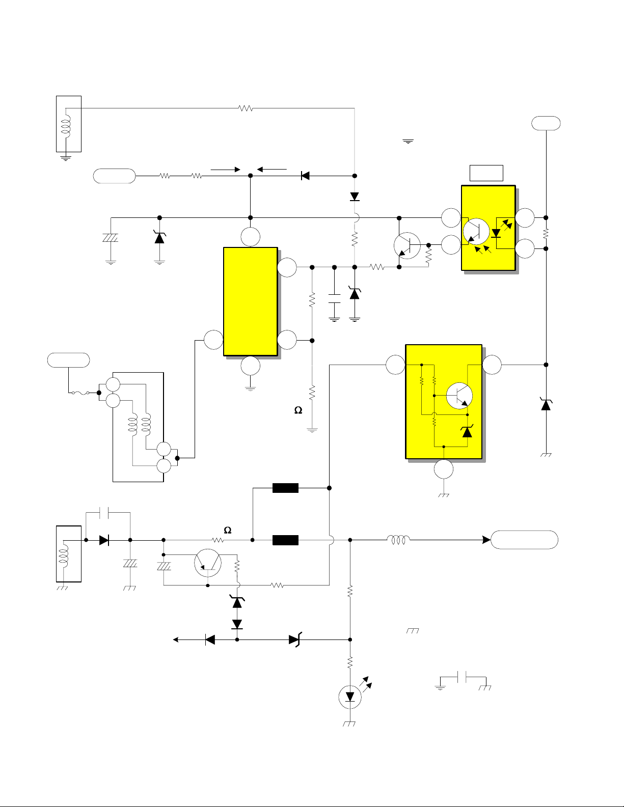
TP01
DP-5X CHASSIS POWER SUPPLY SW +115V REGULATION
High Voltage Power Supply
9
7.5P/P
8
1 of 3
Supplied from Relay S903
AC Supplied from
Relay S903
Raw B+ from DP01 Pin 1
150V
FP01
AC
From LP06 pin 4
CP07
TP01
1
2
5A
DP02
163.6V
RP02RP01
Start Up
19.3V
Output IC
3 2
DS
RP11
4
VIn
OCP/FB
IP01
Driver/
Gnd
5
Run
Osc B+
1
RP09
RP05
0.05
DP03
2.3V
RP10
CP09
DP04
QP01
RP12
DP05
B+ 115V
Hot Ground from
pin 8 of TP01
FB
19.3V
4.4V
RP14
IP02
4
3
Regulator
Photocoupler
IP40
1 2
12V
11.3V
1
RP51
2
10.4V
11.2V
DP53
TP01
17
16
3 of 3
CP45
DP46
CP51
2 of 3
CP59
X-Ray
Protect
5
6
QP41
RP47
0.39
DP55
DP56
DP57
RP49
EP46
0.5K
3K
EP45
RP48
DP58
RP55
Deflection
B+ 115V
RP54
DP59
LP47
3
0.85A
SW +115V
Cold Ground from
pin 16 of TP01
CP01
Page 01-01
Page 8
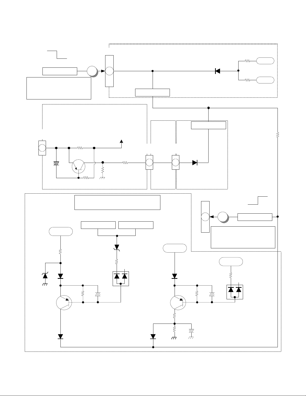
DP-5X PROTECT-OVP SHUTDOWN BLOCK DIAGRAM
Signal Power
Sheet 14
From QJ06
RE35 Current Sensor
VM 220V
Over Current Det.
PPT3
10.5V
Turns on Relay S902
3
D950
10.5V Too High Det.
Activated De t .
To Q943
DJ14
Prot-OCP
Power 1
D990D988
PPT3
Turns on Relay S901
Signal Power
Sheet 14
7
C
RJ16
To Q942
Power 3
Q980
AC Too High Det.
< Protect >
< Prot >
10.5V Loss Det.
D951
D959
DJ09
PPT3
2
From Q901 / I905
Signal Power
Sheet 14
From QJ02
DM/Power/IF
Sheet 4
QE08
ERG1
7
AB
< VM Port > < CRT Prot >
Green
Red CRT
Sheet 12
CRT
Sheet 11
RP40
Def + 28V
DP48
Def - 28V
RP41
From Voltage Divider
RP54, RP55 off
Def. +115V
Current Sensor RP47
From QP41 off
Def. +115V
Deflection Power
Sheet 15
VM Overcurrent
Detection
PCT
DX15
3
RGB Processor
Sheet 6
DP60
Def -28V Loss
Detection
Excessive Def. B +
Detection
DP56DP55
Excessive Def. B +
Current Detection
< Prot-OVP > < Prot-OVP >
B
1
PDT3
DP61
R632
A
DP57DP58
High Voltage Det.
-5V Loss Detection
DC33
-5V Loss Det.
DC/DEF/IF
Sheet 7
D608
Vert. 26V
Overcurrent Det .
DH15
Excessive
RC51
+ 5V
- 5V
RC50
From Q604
and Current Sensor
R609
From DH13, CH17
off Pin 7 of Flyback
Deflection
Sheet 17
PAGE 01-02
Page 9
CP45
TP01
DP46
17
CP51
16
Deflection B+ (115V)
Excessive Current Det.
CP59
DP-5X PROTECT-OVP (A) DIAGRAM
EP46
500
3K
EP45
RP54
RP55
QP41
RP47
0.39 Ohm
RP48
DP55
RP49
DP58
Deflection B+ 115V
Def +115V
Deflection B+ (115V)
Excessive Voltage Det.
DP59
TP01
TP01
13
15
14
10K
EP41
10K
EP40
RP53
SW-28V Short or Loss Det.
CP41
DP42
CP47
CP40
DP40
CP46
CP63
DP48
RP40
-
+
LP40
+
RP46
DP56
D926
LP41
CP52
1
CP53
Def 7.5V
2
A
RP41
-
+
+
-
DP60
DP61
QP40
3
PROT-OVP
2000
EP47
LP43
LP42
LP46
See Protect-OVP (A to B)
Shutdown Circuit Diagram
for continuation.
0.65A
1.26A
PDC1
3
0.69A
SW -28V
KPGnd
SW +28V
Def 6.3V
DP50
DP51
PAGE 01-03
Page 10
DP-5X PROTECT-OVP (A to B) SHUTDOWN DIAGRAM
RH32 allows ABL fluctuations to
manipulate the Trigger Point of Shut
Down as screen brightness varies. ABL
is inverse proportionate to brightness.
This prevents false triggering.
Vertical Output Circuit
I601
Vs
10
L603
C604
Q604
ABL
Excessive Hi
Def +28V
R629 0.68 Ohm
Voltage Det.
ABL Voltage
Too High Det.
LH01
RH21
RH32
RH24
DH15
1
3
A
Flyback
TH01
8
RH25
< Prot-OVP >
High Voltage
Sensing Circuit
5OP
RH23
LH06
DH13
RH26
DH14
77
OVP
1
Stops H. Drive
29.01V
CH17
Any fluctuations in High Voltage will
also be reflected by the 50P output P/P.
By monitoring the 50P (50 Pulse) rises
in High Voltage will be sensed. If High
Voltage climbs too high, DH15 will fire
and trigger a shut down event.
See Protect-OVP (A)
Shutdown Circuit Diagram
for Inputs.
Hi Volt
H. Drive
IH01
R630
C610
Excessive Vertical
Current Det .
If the Vertical Output IC has a problem,
R629 will sense the current rise. The
voltage drop will be reflected at the base
of Q604 turning it on and producing a
Shut Down high.
R631
D608
R632
1
Deflection Sheet 17
PDT3
1
Active
Normal
5
B
< Prot-OVP >
See Power Supply Shut Down
Circuit Diagram for continuation.
See Protect-OVP (B to C)
Shutdown Circuit Diagram
for continuation.
PAGE 01-04
Page 11
DP-5X PROTECT-OVP (B to C) SHUTDOWN DIAGRAM
Active
Normal
< Prot-OVP >
See Protect-OVP (A to B)
Shutdown Circuit Diagram
for inputs.
CRT +220V Excessive
Current Detection
PDC1
Def
+220V
1
CE10
From Deflection
Sheet 17
5
B
RED CRT PWB Sheet 12
RE35
2.2 Ohm
QE08
RE29
PDT3
1
To CRT 220V
To VM Circuit
RE31
RE34
VM PORT
15
< Prot-OVP >
6
GREEN
CRT PWB
Sheet 11
ERG1
A B
7
VM PORT
PCT
3
CRT PROT
-5V Loss Detection
< Prot-OVP >
DX15
1
DC33
-5V Loss Det.
On DC/DEF/IF Sheet 7
7
RGB
Processor
Sheet 6
RC51
+ 5V
- 5V
RC50
RJ16
DJ16
QJ06
Def + 7.5V
See Protect-OCP Shutdown Circuit
Diagram for Inputs
From DC/DEF-I/F
Sheet 7
From RGB Processor
< Prot-OCP > < Prot-OCP >
2
DJ04
RJ32
RJ31
DJ15
RJ3O
DJ06
CJ08
OVC Activated
Detection
DJ15
Sheet 6
DJ09
QJ02
RJ18
RJ19
Sig + 5.6V
PPT3
7
DJ08
RJ17
Sig +10.5 V Loss
Detection
CJ03
Normal
10
C
< Prot-OVP >
See Protect-OVP (C)
Shutdown Circuit Diagram
for Continuation.
Sig + 10.5V
RJ08
CJ04
DJ07
From DM/POWER/I/F
Sheet 4
Active
3
PAGE 01-05
Page 12
DP-5X PROTECT-OCP DIAGRAM
1
< Prot-OCP >
RGB Processor
Sheet 6
Shuts Off VM
Driver Circu it
through QX20
QX26
RY13
RY14
CX58
VM Gain
Cont
Deflection +10.5V
Short Detection
On Deflection
Sheet 17
PCT
2
Green
CRT PWB
Sheet 11
Gain
Cont
D723
EGB1
8
Def 10.5V
Blue CRT PWB
Sheet 10
To VM Output
Circuit QEA6
CEC1
ba
REF6
Gain
Cont
PDT3
1
2
VM Excessive
Current Detection
15 Ohm
REF4
REF5
REE9
Def 10.5VDef 10.5V
0.15A
On Deflection Power
Sheet 15
On DC/DEF/IF
Sheet 7
REF1
QEA8
< Prot-OCP >
REF2
ERG2b
2
VM
+220V
On DM/POWER/IF
Sheet 4
DJ16
QJ06
DJ15
Def + 7.5V
2
RJ32
DJ15
RJ3O
OVC Activated
Detection
PROT-OVP
< Prot-OCP >
2
DJ04
RJ31
DJ06
CJ08
See Protect-OVP (B to C)
Shutdown Circuit Diagram
for continuation.
PAGE 01-06
Page 13

DP-5X PROTECT-OVP (C) SHUTDOWN CIRCUIT
For
Signal
Power
Supply
D902
Relay
Driver
SBY +5V
AC
Q943
From Sub
Micro
Pin 20, Q021, Q025 Pin 81
Power 12Power 3
6
onoff
S90207
D941
R944
D946
D945
R941
From Digital
Module
onoff
R947R946
SBY +5V
D942
D958
S903
R943
D944
AC
2.2 ohm
F904
PPT3
PPT3
D940
Q942
R940
3
SBY +5V
S901
S904
D943
11 12 13
For
AC
Signal &
Deflection
Power
Supply
S902
S903
Relay
Driver
Audio B+
Audio
Vcc
Audio Vcc
See Protect-OVP (B to C)
Shutdown Circuit Diagram
AC
Hot
Ground
AC 175 On
Raw B+
D902
AC
for Inputs.
R924
R925
D915
9V
R927
C916
<PROTECT>
1
2
4
5
T902
(8.9V ~ 9.3V)
R926
C
7
Normal
10
Active
Page 01-07
D950
R980
Q980
R945
D951
C980
C981
To Sub Power
D948D947
Q981
R982
R981
12
R942
Q944
Relay
Driver
Q901
Sig +10.5V
Run B+ 16V
D988
D990
1
Excessive Sig +10.5V
Voltage Detection
I905
2
1 3
R923
D959
AC Voltage Too High
SBY 5V
4
1
10
Detection
Page 14

DP-5X BLANK PAGE “USE FOR NOTES”
BLANK PAGE
Page 15

VIDEO
INFORMATION
DP-5X
CHASSIS INFORMATION
SECTION 02
Page 16

DP-5X BLANK PAGE “USE FOR NOTES”
BLANK PAGE
Page 17
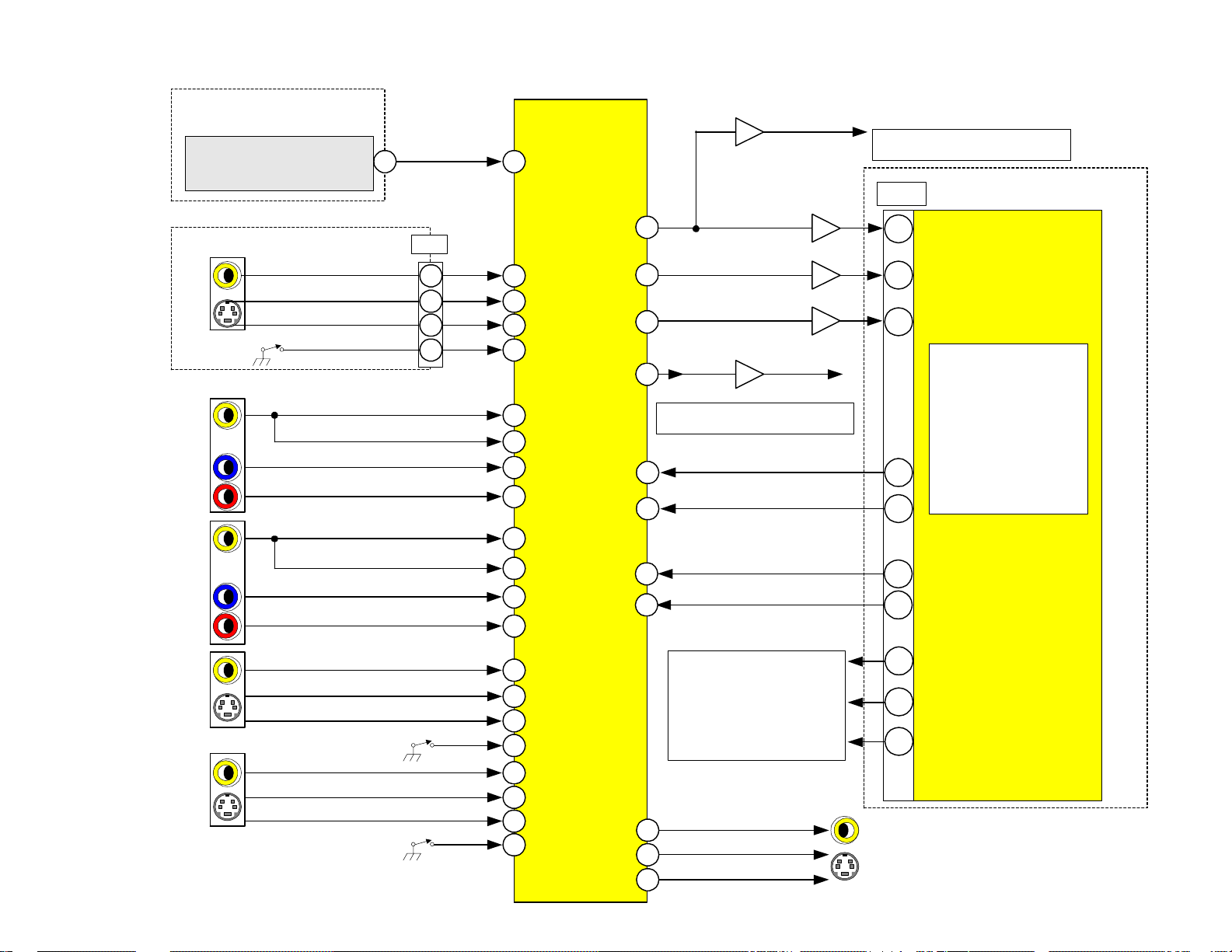
DP-5X CHASSIS VIDEO SIGNAL SELECTION PATH CIRCUIT DIAGRAM
Tuner Sheet 2
U301 Main Tuner
Sheet 13
Front Control PWB
V5
S5
V4
V3
TUNER
Aux 5 Video V3V
Aux 5 S-Y V3Y
Aux 5 S-C V3C
S-5 Det.
Component 4 Y
Composite 4
Component 4 Pb/Cb
Component 4 Pr/Cr
Component 3 Y
Composite 3
Component 3 Pb/Cb
Component 3 Pr/Cr
13
1 2
PFT
2
7
9
AV Selector Sheet 3
I401
Video Select
15
TV1_CV
65
V1
67
Y1
69
C1
S-1
CY2
V8
PB2
PR2
CY1
V7
PB1
PR1
SUB OUT
Y5 DM In
C5 DM In
7011
27
19
29
31
21
17
23
25
MAIN
OUT
Y
C Pb
C Pr
Y
SDA5
SCL5
Composite Video or S-Y
For Micro. CC detection
Main Y / V
Q407
Q408
56
Q409
55
Q410
54
Q403
60
Sub Y / V
See Sub Sync Signal Path
SD YO
11
NTSC for Monito Out
13
SD CO
45
46
See Main Sync Signal Path
PST
56
80
DM / Power / I/F
Sheet 4
Main Y/CV
Main Pb/C
Digital
Module
2
Main Pr
INCLUDES:
ATSC / QUAM Tuner
3D Y/C
PinP Section
HDMI Input
CableCard Input
48
49
54
53
Optical Audio Out
Flex Converter
SDA5
SCL5
V2
S2
PAGE 02-0 1
V1
S1
Aux 2 Video
Aux 2 S-Y
Aux 2 S-C
S-2 Det.
Aux 1 Video
Aux 1 S-Y
Aux 1 S-C
S-1 Det.
77
79
71
73
75
76
V3
Y3
C3
1
2
S-3
V2
Y2
MON OUT
C2
S-2
V Out 3
Y Out 3
C Out 3
51
52
50
For Continuation
of the Signal Flow
See Video Out Of the
Digital Module
Signal Diagram
Monitor Out Video
Monitor Out S-Y
Monitor Out S-C
MON
OUT
66
67
68
HD_Yo
HD_PBo
HD_PRo
Page 18

DP-5X Chassis Video From The Digital Module Ci r cuit D iagr am
From
Video
Signal
Selection
Path
Signal
Diagram
PAGE 02-02
P
S
T
56
80
2
Main Y/C V
Main Pb/C
Main Pr
Digital
Module
INCLUDES:
ATSC / QUAM Tuner
3D Y/C
PinP Section
HDMI Input
CableCard Input
Optical Audio Out
Flex Converter
SDA5
SCL5
HD_Yo
HD_PBo
HD_PRo
P
S
T
54
53
66
67
68
Y
Pb
Pr
QX11
QX10
QX09
RAINFOREST I C
IX01
RGB
Processor
SDA5
28
SCL5
30
68
Cr1/Pr 1_In
67
Cb1/Pb 1_In
66
Y 1_In
R Out
G Out
B Out
12
13
14
SW+ 9.3V
RY25 RY27 RY28 CX64
RY26
CX63
RY24RY19
SW+ 9.3V
RY40 RY42 RY43 CX68
RY41
CX67
RY39RY34
SW+ 9.3V
RY55 RY57 RY58 CX72
RY56
CX71
RY54RY49
QX29
QX30
QX29
QX34
QX37
QX38
RY29
RY44
RY59
DX05
DX06
DX07
PCT
5
To
CPT
PWBs
7
To
CPT
PWBs
9
DM / Power / I/F
Sheet 4
RGB Processor
Sheet 6
Page 19
DP-5X CHASSIS VIDEO MUTE GENERATION CIRCUIT DIAGRAM
DC/DEF/IF
Sheet 7
AC SIGNAL From
DM/POWER/IF Sheet 4
From QJ04
TO RGB PROCESSOR
Sheet 6
V_MUTE 1
TO AUDIO OUT
Sheet 5
V_MUTE 2
C
QC01
Sheet 9
Mutes Dig Conv.
IS07, IS05
Def +10.5V
DC32
RC12
RC14
DC16
QC05
RC11
B
RC13
CC04
From Sweep Loss
Detection Circuit
QC07 & QC12
QC04
AC Det
Normal Off
RES
A
CC02
Sheet 8
Mutes Dig Conv.
IT01
RC66
CC29
PDT3
Mute
QC17
RC65
CONV. OUT
Sheet 16
9
Mutes
Convergence
Outputs
DEFLECTION
Sheet 17
Shuts off IH01
High Voltage
Driver IC
SW +9.3V
QC02
RC06
RC02
DC14
RC07
CC02
QC03
RC08
DC15
AC Det
Prot HV
V Mute
V Mute
PDT2
4
Prot HV
RC03
PAGE 02-03
Digital
Module
V_MUTE
DM/POWER/IF
Sheet 4
AC Det = Loss of AC
Prot HV = Loss of H or V Sweep
6
D
V Mute = Channel Change, Power
Off/On, Auto Programming, etc..
Page 20
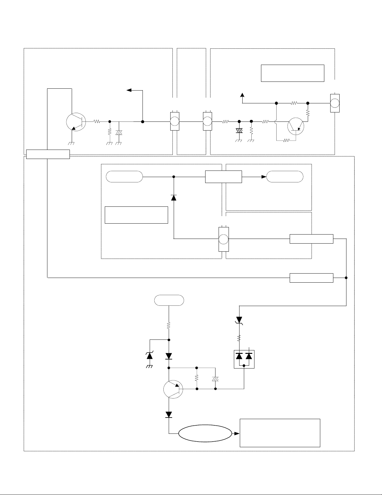
DP-5X ABL CIRCUIT EXPLANATION
(See ABL Circuit Diagram on the next page for details)
The ABL voltage is generated from the Flyback transformer TH01 ABL pi n (8). The ABL pull-up resistors are
RH27 and RH28. They receive their pull up voltage from the SW +115V which is the B+ line for Deflection cre-
ated in the Power Supply.
ABL VOLTAGE OPERATION
The ABL voltage is determined by the current draw through the Flyback transformer. As the picture brightness
becomes brighter or increases, the demand for replacement of the High Voltage bei ng consumed is greater. In
this case, the Flyback will work harder and the current through the Flyback increases. This in turn will decrease
the ABL voltage. The ABL voltage is inversely proportionate to screen brightness.
Also connected to the ABL voltage line is DH16. This zener diode acts as a clamp for the ABL voltage. If the
ABL voltage tries to increase above 10.5V due to a dark scene which decreases the current demand on the flyback, the ABL voltage will rise to the point that DH16 dumps the excess voltage into the 10.5V line.
ACCL TRANSISTOR OPERATION
The ABL voltage is routed through the PDT2 connector pin 3 to the Signal PWB. Then the ABL voltage is
routed through the acceleration circuit RX45 and DX01 to the base of QX12. Under normal conditions, this transistor is nearly saturated. QX12 determines the voltage being supplied to the cathode of DX00, which is connected to pin 78 of the Rainforest IC, IX01. During an ABL voltage decrease due to an excessive bright circum-
stance, the base of QX12 will go down, this wi ll drop the emitter voltage which in turn drops the cathode voltage
of DX00. Thi s in turn will pull voltage away from pin 78 of the Rainforest IC, IX01. Internally, this reduces the
brightness, contrast and color gain voltage which is being controlled by the I
Microprocessor arriving at pins 28 and 30 of the Rainforest IC and reduces the overall brightness, preventing
blooming as well as reducing the Color saturation level to prevent color smear.
ABL SWITCH QH03 AND QH05
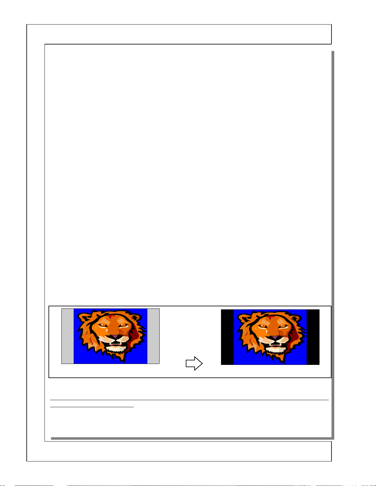
This chassis has the ability to change the Side Panels when watching a NTSC 4X3 image. When a 4X3 images is
displayed on a 16X9 set, the sides do not reach the edges. To avoid excessive ageing at the 4X3 display area, the
side panels IRE levels are raised. However, sometimes the customer may want to turn the side gray panels off.
Through the Video Advanced features Menu the customer can do this. When the Side panels are turned off, the
overall average ABL level for the image is reduced. To compensate, QH03 ABL Switch is turned on. The Microprocessor in the Digital Module tells the Sub Microprocessor IC I001 via I
from the DAC lines pin 88 or 89. This high is routed through the PPT2 connector, either pin 1 or 2, to the base
of QH03 or QH05 turning either one On. This adds either Resistor RH42 or RH43 to the ABL pull up circuit
and the ABL level drops slightly to compensate for the loss of brightness when the side panels go black.
2
C bus data communication from the
2
C communication to output a high
Black Side Panels
Turned on by the
customer
Gray Side Panels
Black Side Panels
RH32 manipulates the trigger point of shutdown dependant upon the ABL level avoiding false triggering.
NOTE: For the Circuit connected to the Xray Protect line, see the PROTECT-OVP (A to B) SHUTDOWN DIAGRAM for details on Page 01-04.
PAGE 02-04
Page 21
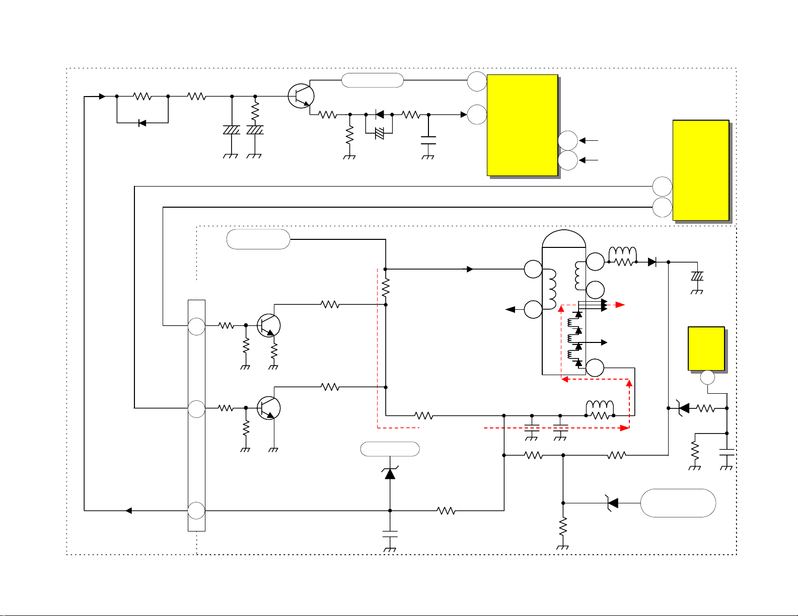
DP-5X Chassis A.B.L. Circuit Diagram
ABL
DX01
RX44RX45
CX23
QX12
RX43
CX22
RX41
RX42
SW +9.3V
DX00
CX21
RX40
ABL
CX20
75
78
IX01
Rainforest
IC
SDA1
SCL1
28
30
I001
Sub
Micro
Signal PWB
Black Panel
89
ABL Switch
88
FBT
SW +115V
ABL_SW
BLACK_
PANEL
ABL switches slightly reduce the
overall operational point of ABL due
to the loss of overall brightness levels.
PDT2
RH30
1
RH35
RH41
2
RH40
RH43 180K
QH03
ABL Switch
RH33
2.2K
QH05
ABL Switch
RH42 47K
Clamp
RH27 24K DP-57
RH27 30K DP-55
Collector of High Voltage
RH27 & RH28
Def +10.5V
PAGE 02-05
ABL
Deflection PWB
To QH01
Output Transistor
ABL Pull-Up
Resistors
RH28 39K
[ Current Path ]
DH16
RD30EB4
RH31
6.8K
B+
9
C
10
CH14
RH32
180K
TH01
50P
CH21
3
As Brightness goes Up, ABL Voltage
goes Down. (Inverse Proportional)
CH18
RH24
43K
LH06
7
RH23
1
Gnd
To Focus
ABL
8
LH01
RH21
RH25 18K
DH15
HZ22-2L
DH13
To
Anodes
CH17
Stops
H. Drive
IH01
OVP
7
DH14
RH26
RH09 CH10
XRay Protect
Page 22

DP-5X BLANK PAGE “USE FOR NOTES”
BLANK PAGE
Page 23

AUDIO
INFORMATION
DP-5X
CHASSIS INFORMATION
SECTION 03
Page 24

DP-5X BLANK PAGE “USE FOR NOTES”
BLANK PAGE
Page 25

Tuner Sheet 2
U301 Main Tuner
Sheet 13
V5
V4
DP-5X CHASSIS AUDIO SIGNAL SELECTION PATH CIRCUIT DIAGRAM
TUNER
TV1-L
TV1-R
Front Control PWB
Aux 5 Audio L
Aux 5 Audio R
AVX 4 Audio L
AVX 4 Audio R
16
1 2
PFT
4
5
C515
C514
C501
C508
C509
C500
AV Selector Sheet 3
I501
Audio Select
35
L2
L Out3
3615
1
2
9
10
MAIN OU T
R2
L3
R3
L7
R7
R Out3
SDA5
SCL5
L10
R10
26
25
22
23
15
16
Q501
Selected Audio Out
Q500
C510
C511
L
R
DM L
DM R
PST
42
43
54
53
45
46
1
3
DM / Power / I/F
Sheet 4
Sel L
Sel R
SDA5
SCL5
SP_L 1
SP_R 1
ATSC / QUAM Tuner
Optical Audio Out
Audio From
Dig Module
Digital
Module
INCLUDES:
3D Y/C
PinP Section
HDMI Input
CableCard Input
Flex Converter
AVX 3 Audio L
V3
V2
V1
AVX 3 Audio R
AVX 2 Audio L
AVX 2 Audio R
AVX 1 Audio L
AVX 1 Audio R
PAGE 03-01
Monitor Audio Out L
MONITOR
OUT
Monitor Audio Out R
C506
C507
C504
C505
C502
C503
C523
C524
C526
C527
7
L6
8
R6
5
L5
R5
6
3
L4
R4
4
L Out 1
30
MON OUT
29
R Out 1
L11
Hi-Fi
R11
17
18
C512
C513
CA36
QA03
QA04
CA48
CA49
CA35
QA01
QA02
4
2
IA02
Audio
Out
Audio
Sheet 5
7
12
PSP
CA60
1
5
CA61
Page 26

SP_R
SP_L
Digital
Module
V_MUTE
AUDIO
MUTE
PST
3
1
6
8
DP-5X CHASSIS AUDIO OUTPUT SELECTION MUTE CIRCUIT DIAGRAM
Right Main Audio
Left Main Audio
D
DA11
DA12
DA13
RA57
RA69
RA58
QA05
QA06
RA59
CA69
CA48
CA49
CA68
QA07
RA60
RA56
RA55
4
2
11
6
CA67
QA08
RA61
IA02
Audio
Out
MUTE
Ripple
Filter
RA62
DA05
7
12
PSP
CA60
1
5
CA61
CA66
DA14
SP_MUTE
SP_OFF
DC/DEF/IF
5
AU+28/39V
RA88
QA13
RA89
Sheet 7
C
V_MUTE 2
QA14
RA90
QA15
RA92
PAGE 03-02
EPG +9V
Audio Out
RA91
Sheet 5
Page 27

DP-5X CHASSIS MONITOR OUTPUT MUTE CIRCUIT DIAGRAM
C512
Hi-Fi Audio
C513
Hi-Fi Audio
V_MUTE 2
From DC/DEF/IF Sheet 7
QC01
DM/POWER/IF Sheet 4
DigitalModule
REC_MUTE
V_MUTE
C523
C524
R536
R537
MONITOR
OUT
17
Hi-Fi Audio L
18
Hi-Fi Audio R
I501
L Out 1
MON OUT
R Out 1
30
29
C526
C527
R545
R546
R538
R541
R539
R542
Audio Select
Q503
C
R547
D502
9
R548
R550
6
D
D503
R555
Q505
SBY+ 5V
R558
R556
Q504
R557
R542
D500
Q502
R543
D501
SPK_MUTE
5
To Audio Output
Sheet 5
R554
PAGE 03-03
A/V SELECTOR
Sheet 3
Page 28

DP-5X BLANK PAGE “USE FOR NOTES”
BLANK PAGE
Page 29

DEFLECTION
INFORMATION
DP-5X
CHASSIS INFORMATION
SECTION 04
Page 30

DP-5X BLANK PAGE “USE FOR NOTES”
BLANK PAGE
Page 31

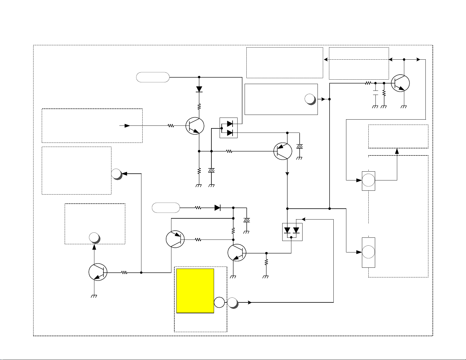
DP-5X SWEEP LOSS DETECTION CIRCUIT
V. Blk.
14V P/P
Vertical Blanking
From Pin 11 I601
From
Deflection
Sheet 17
Horizontal Blanking
From Q706 Emitter
8V P/P
H. Blk.
PDT2
11
7
RC23
CC08
CC09
RC24
Cut Off
QC06
RC26
CC10
RC30
From Pin 79 I001 SUB MICRO Sheet 1
RC25
DC27
RC22
V Det
QC10
CC06
DC26
RC27
RC18
RC29
RC32
DC29
DC28
H Det
RC19
DC25
QC11
QC08
RC31
RC28
RC21
CC13
RC20
QC09
DEF +10.5V
DC32
QC07
RC15
DEF +7.5V
DC/DEF/IF
Sheet 7
RC38
DC31
QC13
RC39
RC37
RC36
DC30
RC34
RC35
CC12
Protect
Switch
QC12
RC33
CC11
See Video Mute
Generation
Circuit
A
Protect HV
PAGE 04-01
Page 32

DP-5X BLANK PAGE “USE FOR NOTES”
BLANK PAGE
Page 33

DIGITAL
CONVERGENCE
INFORMATION
DP-5X
CHASSIS INFORMATION
SECTION 05
Page 34

DP-5X BLANK PAGE “USE FOR NOTES”
BLANK PAGE
Page 35

Magic Focus
Ft. Control PWB
Sheet 13
1
IR Out
HMO1
IR Receiver
3
PAGE 05-0 1
IR Out
HMO2
IR Receiver
SM09
DM11
QM05
DM18
DP-5X CHASSIS "DIGITAL CONVERGENCE" INTERCONNECTION CIRCUIT DIAGRAM
I006
3
4
2
3
2 1
PFT1
21
3
Q030
1
5
8
2
PFS
Q020
1
6
IR In
Stby
+3.3V
I001
98
MAG SW In (Lo)
25
IR Out
90
DCU IR Sel
IR
1
91
Digicon Adj
Magic Sw Out
Sub Micro
DC/DEF/IF
Sheet 7
SUB MICRO
Sheet 1
SENSOR PW B
Sheet 18
LED
S0 ~S7
8 Total
Sensors
+5V
Digicon
Busy In
BUSY
95
92
SC01
Service
Only
From QC16
From IC01
PSET
10
Gnd
9
S7
8
S6
7
S5
6
S4
5
S3
4
S2
3
S1
2
S0
1
SUB MICRO
Sheet 1
-5V
+5V
5
IS04
3.3V Reg
Sw Adj
DM/POWER/IF
Sheet 7
PST
Dig Mod
HD_Yo
HD_PBo
HD_PRo
DC_B
DC_G
DC_R
DC _YS
DC_YS
DC_Busy
Magic SW 2
DC Adj 2
DC_IR 2
SW_ADJ
CONVERGENCE DIGIT AL
V Blk 2
H Blk 2
DC_Size
DC_R
DC_G
DC_B
54 90 125
S7
S6
S5
S4
S3
S2
S1
S0
66
67
68
53
50
49
48
66
60
61
25
59
DIG
Sheet 8
18
47
35
33
27
65
3 12
75
76
77
78
79
80
1
2
IS06
IS07
IS06
IS07
Rainforest
QX09
QX13
Includes
OSD
QX10
QX11
QX16
QX15
QX14
66
HD_Y0
67
HD_Pb
68
HD_Pr
26
Dig OSD B
25
Dig OSD G
24
Dig OSD R
2 YS3
IX01
PDT4
Def+28P
1
RV
IT04
7
1
RH
7
6
DIG
CONVERGENCE
ANALOG
Sheet 9
-5V
+5V
GV
GH
BV
BH
5
4
3
2
DK35
Mute
DK70
Mute "Lo"
7
IT06
1
7
IT02
1
IT01
45
7
RES
DT01
Mute
DK70
Mute
RK77
RK76
IK02
2
RGB PROCESSOR
B
14
G
13
R
12
13
IK40
6
RV
12
18
RH
3
7
GV
19
Def-28P
13
6
GH
12
7
3
BV
19 20
18
BH
13
RK12
Sheet 6
QY38
QX34
QX30
14
-
+
10
-
+
22
-
+
5
CONVER OUT
5
IK41
10
-
+
22
-
+
14
-
+
RK11
DK36
CYV+
15
CYV-
17
CYH+
11
CYH-
8
23
20
Sheet 16
11
8
CYV+
23
CYV-
CYH+
15
17
Def+28V
CYV+
CYV-
CYH-
CYH+
CYH-
PCT
9
7
5
PCR
1
3
6
4
PCG
1
3
4
6
PCB
1
3
4
6
B
To CRTs
G
R
To Red Convergence Yokes
To Green Convergence Yokes To Blue Convergence Yokes
Page 36

DP-55 REMOTE CONTROL CLU-4351UG2 (p/n HL02072)
When Convergence is
adjusted by this Remote,
this Remote must be changed
to DCU mode.
Remote begins in TV mode.
Press and hold the "TV" key.
Press all at one time, "MENU,
INFO and (-) DASH" keys.
POWER
VCR
INPUTS ASPECT PIP
CBLDVD
TV
SAT
DAY/NIGHT
To return to normal TV mode.
Press and hold the "TV" key.
Press the "0" then "1" keys.
ROM WRITE
ROM READ
(Read Old ROM Data)
BLUE Select
13X9 Mode
(5 Times)
REMOVE COLOR
Outside Signal + Gr i d
Outside Signal + Curso r
Outside Signal w/o Cursor
NOTE: Sensor Error Code place
in DCAM, place TV in DCAM,
press DAY/NIGHT then
CURSOR UP
CURSOR DOWN
CURSOR LEF T
RED Select
7X5 Mode (5 Times)
MENU
SELECT
VOL
FAV CH
MUTE
1
2 3
4 5 6
7 8 9
EXIT
CH
GUIDE
INFO
SINGLE CROSSHAIR
CROSSHATCH / V I DEO
(5 Times)
ADJUSTMENT
CALCULATION
GREEN Select
3X3 Mode (5 Times)
CH UP Moves
Adjustment Poi n t
Counter Clockwise
Spiraling Outward
CH DW Moves
Adjustment Poi n t
Clockwise Spiraling
Inward
INITIALIZE
RASTER POSITION
NOTE: The 3X3 mode can only
be entered after the RAM is
cleared.
With Power Off press and hold
the Service Only switch.
Then Press the Power Button.
0
HITACHI
CLU-4351UG2
LC
CURSOR RIGHT
Removes
Adjustment Marker
DCU PHASE
NOTE: DCU Phase
Press
then the EXIT key
PAGE 05-02
Page 37

DP-57 REMOTE CONTROL CLU-3842WL HL02062
When Convergence is adjusted
by this Remote,
this Remote must be changed to
DCU mode.
Remote begins in TV mode.
While holding the "ENT" key,
press "MENU" then "INFO" keys.
TV LED will blink 3 times.
Can not change Source Access.
INITIALIZE
(Aspect then Stop) Keys
Pressed by itself produc e s
extra lines at outside edge.
TV DVD CBL STB PVR AMP
SOURCE ACCESS
ENT
ASPECT
DAY/NIGHT
PIP
To return to normal TV mode.
Remote begins in TV mode.
Hold down the ENT key and
enter 1345 (Hitachi Pre-Code).
RASTER POSITION
Volume Up and Down is a Wheel.
Pressing acts as a button for MUTE.
Channel Up and Down is a Wheel.
Pressing acts as a button for
FAV CH (Favorite Channel).
ROM WRITE Press twice.
CALCULATE
REMOVE COLOR
Outside Signal + Gr i d
Outside Signal + Curso r
Outside Signal w/o Cursor
ADJUSTMENT
DCU PHASE in DCAM
then press EXIT
MUTE Clears Warning Displays
NOTE: Sensor Error Code place
Remote and TV in DCAM,
press DAY/NIGHT then
ADJUSTMENT POINT UP
ADJUSTMENT POINT DOWN
ADJUSTMENT POINT LEFT
GUIDE
SELECT
C.C. INFO
INPUTS
VOL
(PUSH TO
MUTE)
CH
(PUSH FOR
FAV CH)
1 2 3
4 5 6
SINGLE CROSSHAIR
ROM READ Press twice.
EXITMENU
(Read Old ROM Data)
CROSSHATCH / V I DEO
(Press 5 Times)
Toggles between Red and
Blue Adjustment Mode
GREEN Select
3X3 Mode (Press 5 Times)
BLUE Select
13X9 Mode
(Press 5 Times)
CH UP Moves
Adjustment Poi n t
Counter Clockwise
Spiraling Outward
CH DW Moves
Adjustment Poi n t
Clockwise Spiraling
Outward
NOTE: The 3X3 mode can only
be entered after the RAM is
cleared.
With Power Off press and hold
the Service Only switch.
Then Press the Power Button.
7 8 9
0
HITACHI
LC
ADJUSTMENT
POINT RIGHT
Removes
Adjustment Marker
RED Select
7X5 Mode
(Press 5 Times)
PAGE 05-03
Page 38

DP-5X REMOTE INTO DCAM
ENTERING THE REMOTE CONTROL INTO THE DIGITAL CONVERGENCE
MODE (DCAM).
To enter the Remote Control into DCAM do the following;
FOR THE CLU-3842WL
Remote must be in the TV mode. Use the ENT left or right to make the TV LED light.
Press and hold down the ENT Key
Press the MENU and then INFO key.
Remote TV LED will blink 3 times to indicate remote in the DCAM.
• Note: The SOURCE ACCESS arrow Left and Right will no longer move the
source to DVD, CBL, STB, PVR or AMP while the Remote is in DCAM.
• Also the LED will not light in DCAM.
FOR THE CLU-4351UG2
Remote must be in the TV mode.
Press and hold down the "TV" button.
Press and hold down the "MENU, INFO and the (-) DASH" button.
Release all at one time.
To return the Remote Control into normal mode do the following;
FOR THE CLU-3842WL
Remote will already be in TV mode.
Press and hold down the ENT key and enter 1345 to select Hitachi pre-codes.
Remote TV LED will blink 3 times to indicate remote in normal mode.
FOR THE CLU-4351UG2
Press and Hold down the "TV" key.
Then press "0" and then "1" keys.
WARNING:
If the Remote Controls are left in the DCAM mode, then there will be problems operating the
TV. One sure way to tell is to test the ASPECT key while the TV is in normal mode. The ASPECT key will not have any effect on the picture. In this case, the remote is in DCAM and
must be returned to normal mode.
Note: * DCAM means Digital Convergence Adjustment Mode.
Page 05-04
Page 39

DP-5X SERVICE ONLY SWITCH LOCATION
The Service Only Switch is located on the Signal PWB this year.
Page 05-05
Page 40

DP-5X GAINING ACCESS TO THE SERVICE ONLY SWITCH
To Get to the Service Only Switch;
1. Remove the speaker grille by grabbing the sides
2. Pulling left and right side see (a) (b).
3. Remove the Screws holding the Front Access Panel to the Cabinet.
4. Remove the Access Panel.
5. The Service Only Switch is located on the Signal PWB located on the Right Side.
• See previous page for location on the Signal PWB.
Page 05-06
Page 41

DP-5X ENTERING DCAM VIA MAGIC FOCUS
ENTERING DIGITAL CONVERGENCE MODE (DCAM) WITHOUT REMOVING
SPEAKER GRILL.
Note: The original Service Manual on page 34 had the wrong procedure. This page was
modified on our web site 12/23/2005.
PROCEDURE: FOR THE CLU-4351UG2
THE REMOTE MUST BE PLACED IN THE "LINE ADJUST MODE" FIRST:
• See Picture of Remote on page 05-03.
To enter the Remote Control into Line Adjust Mode do the following;
Press all 4 keys and hold down [ TV ] + [ ASPECT ] + [ 9 ] + [ INFO ] button.
Release all the keys.
Remote is now in Line Adjust Mode.
To enter DCAM using the Remote Control do the following;
Remote is still in Line Adjust Mode
Press the STOP [ ■ ] button.
TV enters DCAM.
THE REMOTE MUST NOW BE PLACED INTO DCAM MODE TO MAKE ADJUSTMENTS:
To enter the Remote Control into DCAM do the following;
Remote must be in the TV mode.
Press all 4 keys and hold down [ TV ] + [ MENU ] + [ INFO ] + [ - ] ( DASH) buttons.
Release all at one time.
Remote is now in DCAM.
Make all necessary Adjustments. Be sure to Save the Data and Initialize the Sensors when
complete.
To Exit the TV from DCAM, Press the PLAY [ ► ] then the [ EXIT ] keys, picture returns to
normal.
To return the Remote Control into normal mode do the following;
Press and Hold down the [ TV ] key.
Then press [ 0 ] then the [ 1 ] key.
WARNING:
If the Remote Controls are left in the DCAM mode, then there will be problems operating the
TV. One sure way to tell is to test the ASPECT key while the TV is in normal mode. The ASPECT key will not have any effect on the picture. In this case, the remote is in DCAM and
must be returned to normal mode.
Note: * DCAM means Digital Convergence Adjustment Mode.
Page 05-07
Page 42

30.5
41.0
82.0
82.0
NOTE: Aspect may not be correct but dimensions are correct.
51 INCH DIGITAL CONVERGENCE OVERLAY DIMENSIONS
51F710A and 51F710R
DP-55 and DP-57 Chassis
OVERLAY DIMENSIONS
1129
19.7
90.8
90.8
90.8 90.8 90.8 90.8 90.8 90.8 90.8 90.8
H. SIZE
19.7
82.0
82.0
82.0
82.0
41.0
30.5
V. SIZE
Centering Offset
RED OFFSET = 20mm
BLUE OFFSET = 25mm
BR
635
PART NUMBER H312272
VERTICAL SIZE = 560mm
HORIZONTAL SIZE = 1070mm
PAGE 05-08
Page 43

NOTE: Aspect may not be correct but dimensions are correct.
57 INCH DIGITAL CONVERGENCE OVERLAY DIMENSIONS
57F710A and 57F710R
DP-55 and DP-57 Chassis
OVERLAY DIMENSIONS
1262
H. SIZE
34.1
45.8
91.7
91.7
22.0
101.5
101.5
101.5 101.5 101.5 101.5 101.5 101.5 101.5 101.5
22.0
91.7
91.7
91.7
91.7
45.8
34.1
V. SIZE
Centering Offset
RED OFFSET = 20mm
BLUE OFFSET = 25mm
BR
710
PART NUMBER H312273
VERTICAL SIZE = 625mm
HORIZONTAL SIZE = 1195mm
PAGE 05-09
Page 44

NOTE: Aspect may not be correct but dimensions are correct.
65 INCH DIGITAL CONVERGENCE OVERLAY DIMENSIONS
65F710A and 65F710R
DP-55 and DP-57 Chassis
OVERLAY DIMENSIONS
1439
H. SIZE
38.6
52.1
104.6
104.6
25.3
115.7
115.7
115.7 115.7 115.7 115.7 115.7 115.7 115.7 115.7
19.7
104.6
104.6
104.6
104.6
52.1
38.6
V. SIZE
Centering Offset
RED OFFSET = 20mm
BLUE OFFSET = 25mm
BR
809
PART NUMBER H312274
VERTICAL SIZE = 710mm
HORIZONTAL SIZE = 1365mm
PAGE 05-10
Page 45

DP-5X MAGIC FOCUS TUNE UP VIA CUSTOMER’S MENU
The Digital Convergence or Manual convergence can be accessed through the Customer's Menu. This section
will outline the Customer's Menu selections under each conditi on.
To Access the Convergence Menu, press the MENU button on the remote control. The Customer's Menu will
appear.
Navigate down by using the Cursor down button
to highlight Setup.
This will bring up the Customer's Setup Menu.
Navigate down by using the Cursor down button
to highlight Magic Focus Tune Up.
With the Magic Focus Tune Up Menu now shown, Navigate down by using the Cursor down button to
highlight Start and press the Select (center button between the cursor keys) and Magic Focus begins.
Page 05-11
Page 46

DP-5X MAGIC FOCUS TUNE UP VIA CUSTOMER’S MENU
Magic Focus begins displaying multi
colored light patters and as the process
advances, the marks below the wording
Magic Focus gets closer and closer together until it completes.
If the "At Turn Off, 90 Days is
checked, the set will automatically enter Magic Focus each 90 days when
the set is turned off.
The Adjustment Mode can also be set
for 9 Point and 117 Point Manual adjustments.
NOTE: Remember, the set must be
turned on for at least 20 minutes before making an Manual adjustments. Allowing time for all circuits
to reach temperature and to stabilize.
9 POINT CUSTOMER'S MANUAL
CONVERGENCE ADJUSTMENT:
This indicates the 9 Point Manual
Mode has been selected. Scroll down
to Start and press the Select button to
begin manual adjustments.
In this mode, 9 points on the screen
can be adjusted Red or Blue.
(Green is never adjusted manually).
Page 05-12
Page 47

DP-5X MAGIC FOCUS TUNE UP VIA CUSTOMER’S MENU
MOVING THE ADJUSTMENT POINT:
The adjustment point can be moved it two ways: (1) using the cursor keys, Note: The cursor must be white. (2)
using the 2, 3, 4 and 6 keys. Note. When moving the adjustment point with the number keys, the adjustment point
changes to Red.
SELECTION THE COLOR TO ADJUST:
Only Red or Blue can be adjusted in manual mode. By repeatedly pressing the Select Key on the remote, the adjustment point changes in the following manner: White ~ Red ~ Blue ~ White.
ADJUSTING THE SELECTED COLOR:
Once the alignment cursor is at the location in need of correction, and while the adjustment cursor is either Red
and/or Blue, use the cursor keys on the remote to make the appropriate correction to the color to make the +
white, with no offending color sticking out.
SAVING THE NEWLY MANUALLY ADJUSTED CONVERGENCE DATA:
When the affected color or mis-convergence is corrected, press the EXIT key on the remote. This will bring up
another menu.
From this Menu, you can do the
following.
CANCEL:
• Highlight CANCEL
and press SELECT,
the Magic Focus Tune
UP menu is canceled
and the picture returns
to the Normal Picture.
DONE:
• Highlight DONE and
press SELECT, the
Magic Focus correction data is stored and
the picture returns to
the Normal Picture.
RESET:
• Highlight RESET and
press SELECT, the Magic Focus correction data is returned to the previous state before any manual adjustments were made. In other words, the old ROM data is re-read and convergence returns to previous
state.
BACK:
• Highlight BACK and press SELECT, and the screen will revert back to the 9 point adjustment screen
were additional adjustment can be made. Press EXIT after making additional adjustments to return to
this screen to Save the newly adjusted data.
NOTE: If the Adjustment mode is return to Auto, all Manual adjustments are lost.
NOTE: If the Magic Focus button is pressed, all Manual adjustments are lost.
The Adjustment Mode can also be set for 9 Point and 117 Point Manual adjustments.
NOTE: Remember, the set must be turned on for at least 20 minutes before making an Manual adjustments. Allowing time for all circuits to reach temperature and to stabilize.
117 POINT CUSTOMER'S MANUAL CONVERGENCE ADJUSTMENT:
This indicates the 117 Point Manual Mode has been selected. Scroll down to Start and press the Select button to
begin manual adjustments.
Page 05-13
Page 48

DP-5X MAGIC FOCUS TUNE UP VIA CUSTOMER’S MENU
In this mode, 117 points on the screen can be adjusted Red or Blue. (Green is never adjusted manually).
MOVING THE ADJUSTMENT POINT:
The adjustment point can be moved it two ways: (1) using the cursor keys, Note: The cursor must be white. (2)
using the 2, 3, 4 and 6 keys. Note. When moving the adjustment point with the number keys, the adjustment
point changes to Red.
SELECTION THE COLOR TO ADJUST:
Only Red or Blue can be adjusted in manual mode. By repeatedly pressing the Select Key on the remote, the adjustment point changes in the following manner: White ~ Red ~ Blue ~ White.
ADJUSTING THE SELECTED COLOR:
Once the alignment cursor is at the location in need of correction, and while the adjustment cursor is either Red
and/or Blue, use the cursor keys on the remote to make the appropriate correction to the color to make the +
white, with no offending color sticking out.
Page 05-14
Page 49

DP-5X MAGIC FOCUS TUNE UP VIA CUSTOMER’S MENU
SAVING THE NEWLY MANUALLY ADJUSTED CONVERGENCE DATA:
When the affected color or mis-convergence is corrected, press the EXIT key on the remote. This will bring up
another menu.
From this Menu, you can do the following.
CANCEL:
• Highlight CANCEL and press SELECT, the Magic Focus Tune UP menu is canceled and the picture
returns to the Normal Picture.
DONE:
• Highlight DONE and press SELECT, the Magic Focus correction data is stored and the picture returns
to the Normal Picture.
RESET:
• Highlight RESET and press SELECT, the Magic Focus correction data is returned to the previous state
before any manual adjustments were made. In other words, the old ROM data is re-read and convergence returns to previous state.
BACK:
• Highlight BACK and press SELECT, and the screen will revert back to the 9 point adjustment screen
were additional adjustment can be made. Press EXIT after making additional adjustments to return to
this screen to Save the newly adjusted data.
NOTE: If the Adjustment mode is return to Auto, all Manual adjustments are lost.
NOTE: If the Magic Focus button is pressed, all Manual adjustments are lost.
Page 05-15
Page 50

DP-5X BLANK PAGE “USE FOR NOTES”
BLANK PAGE
Page 51

CHASSIS
PICTURES
DP-5X
CHASSIS INFORMATION
SECTION 06
Page 52

DP-5X BLANK PAGE “USE FOR NOTES”
BLANK PAGE
Page 53

DP-5X CHASSIS PICTURE
Page 06-01
Page 54

DP-5X CHASSIS PICTURE
Page 06-02
Page 55

DP-5X CHASSIS PICTURE
Page 06-03
Page 56

DP-5X CHASSIS PICTURE
Page 06-04
Page 57

DP-5X CHASSIS PICTURE
Page 06-05
Page 58

DP-5X PRODUCT INFORMATION
DP-5X REAR INPUT PANEL
DP-5X FRONT INPUT PANEL
DP-5X REMOTE CONTROL CLU-4351UG2 (p/n HL02072)
Page 06-0
6
Page 59

TROUBLE
SHOOTING
DP-5X
CHASSIS INFORMATION
SECTION 07
Page 60

DP-5X BLANK PAGE “USE FOR NOTES”
BLANK PAGE
Page 61

DP-5X TROUBLESHOOTING
SIGNAL POWER SUPPLY P.W.B.
Preparation for adjustment :
• Set the AC input power supply to 120V ±1V.
• Receive a Crosshatch pattern signal.
• Set the Contrast, Brightness controls to maximum.
• Heat Run for at least 30 seconds after the power is turned on.
• Audio : Mute.
Adjustment procedure
• Check the voltage of the Power supply as shown in the table below.
• When the power switch SM01 is turned ON, check that the relay is also turned ON.
• If using a dummy load, it is necessary to short S901 primary side terminal by jig.
Remarks The power supply voltage should be normal. There should be no abnormal operation of the protection
circuit. (Latch) There should be no parts that generate an abnormal amount of heat. Make sure that there’s no
burning smell or smoke.
Table 1-1. DP55 and DP-57 Chassis
No.
Description Measuring point
+ side - side
Hitachi Circle Pattern
B/C max voltage spec
Dummy load
(Ω) (W)
SET load
(In Amps)
(reference)
1 SBY+5V C957 (+) C957 (-) 5.0 +/-0.2 89 0.5 0.056 A
2 Sig+5.6V C951 (+) C951 (-) 5.8 +/-0.2 2 18 2.86 A
3 Sig+10.5V C947 (+) C947 (-) 10.5 +/-0.5 8 15 1.3 A
4 Audio Vcc C 945 (+) C945 (-) 31-35 Audio mute 440 5 0.08 A
Protection Circuit check
POWER SUPPLY PROTECTION
Apply a 1K ohm short to ground from PPT3 pin 7 (Sig +5.6V line).
S901 should turn off but this is not a Latch state
(Power back on by remote control 2
• 1st push power off.
• 2nd push, power on.
nd
push).
Page 07-01
Page 62

DP-5X TROUBLESHOOTING
DEFLECTION POWER SUPPLY P.W.B.
Preparation for adjustment :
• Set the AC input power supply to 120V ±1V.
• Receive a Crosshatch pattern signal.
• Set the Contrast, Brightness controls to maximum.
• Heat Run for at least 30 seconds after the power is turned on.
• Audio : Mute.
Adjustment procedure
• Check the voltage of the Power supply as shown in the table below.
• When the power switch SM01 is turned ON, check that the relay is also turned ON.
• If using a dummy load, it is necessary to short S901 primary side terminal by jig.
Remarks The power supply voltage should be normal. There should be no abnormal operation of the protection
circuit. (Latch) There should be no parts that generate an abnormal amount of heat. Make sure that there’s no
burning smell or smoke.
Table 1-1. DP55 and DP-57 Chassis
No.
Description Measuring point
+ side - side
DEF+28V
1
DEF-24V
2
DEF+12V
3
DEF+7.5V
4
DEF+6.3V PPC1 (3)
5
DEF+220V PPC1 (1)
6
SW+115V CH16 (+)
7
CP46 (+) CP46 (-) 28 +/-1.5 28 30 1.0 A
CP47 (+) CP47 (-) -24 +/-1.5 33 20 0.75 A
CP48 (+) CP48 (-) 11 +/-0.5 193 1 0.06 A
CP49 (+) CP49 (-) 7 +/-0.5 8.5 6 0.83 A
PPC1 (4) 6.3 +/-0.2 9.1 4.4 0.69 A
PPC1 (4) 226 +/-2.0 1510 35 0.15 A
CH16 (-) 115 +/-1.5 140 100 0.825 A
Hitachi Circle Pattern
B/C max voltage spec
Dummy load
(Ω) (W)
Protection Circuit check
POWER SUPPLY PROTECTION
Apply a 1K ohm short circuit across DP58.
S901 should turn off but this is not a Latch state
(Power back on by remote control 2
nd
push).
SET load
(In Amps)
(reference)
• 1st push power off.
• 2nd push, power on.
Page 07-02
Page 63

DP-5X TROUBLESHOOTING
CONFUSED CROSSHATCH FROM DCU.
If Position Shifted Crosshatch (as show Figure 1) is displayed, check next items.
1. Execute "2-1 Write Standard Data (ltem # 1)"
2. Check DCU Phase Data
Figure 1 Example Image of Position Shifted DCU Crosshatch
If Confused Crosshatch (as show Figure 2) is displayed, check next items.
1. Assembly Error of DCU uCOM (IS07), EEPROM (IS01, ISOS**1), DCU LSI (IS06) , DAC
(IT01), PDT4 connector, or other peripheral parts
2. Solder-Bridge of DCU uCOM (IS07) pins 1, 2, 17, 24, 27, 32, 42, 49, 51, 55, 75 or 80.
3. Solder-Bridge of EEPROM (IS01, IS03*)
4. Solder-Bridge of DCU LSI (IS06) pins 5, 7, 14, 20, 25, 33, 35, 38, 39, 48, 50, 52, 60, 64, 79,
84, 88, 103,110, 111, 118, 125,128 or 142.
5. Solder- Br i dge of DA C (IT01) pins 1, 5, 8, 9, 12, 13 , 16, 17, 32, 33, 36, 37, 40, 41 , 46 , 47 or
48.
6. Solder-Bridge of PDT4 connector
7. "H.BLK/V.BLK" signal line (from PDT2 connector pins 7 or 11 to DCU LSI (IS06) pins 33 or
35.
8. PLL of DCU LSI (RS65, RS67 or CS32)
9. +5V Power supply line (from PDT3 connector pins 10 or 11 to DCU LSI (IS06))
10. +3.3V Power supply line (from +3.3V Regulator (IS04) pin 4 to DCU LSI (IS06))
Figure 2 Example Image of Confused DCU Crosshatch
Note
*1 : IS03 (EEPROM) is only use by DP5X chassis.
Page 07-03
Page 64

DP-5X TROUBLESHOOTING
CONFUSED CROSSHATCH FROM DCU.
If No Correction Crosshatch (All channels, as show Figure 1) is displayed, check next
items.
1. Execute "2-1 Write Standard Data (ltem # 1)"
2. Assembly Error of Reset 1C (IS05), DCU LSI (IS06), DAC (IT01), or other peripheral parts
3. Solder-Bridge of DCU LSI (IS06) pins 5, 7,14, 20, 25, 27, 29, 33, 35, 44, 52 or
88.
4. Solder-Bridge of DAC (IT01) pins 4, 5, or 45.
5. "Mute" signal line (from QC17-C to DAC (IT01) pin 45)
6. +5V Power supply line (from PDT3 connector pins 10 or 11 to DAC (IT01))
Figure 1 Example Image of No Correction DCU Crosshatch
If No Correction Crosshatch (Only one or two colors) are displayed, check next items.
1. Assembly Error of DCU LSI (IS06), DAC (IT01), Op-Amp (IT02 through IT07), PDT4
connector, or other peripheral parts
2. Solder-Bridge of DCU LSI (IS06) pins 60, 64, 79, 84, 98 or 103.
3. Solder-Bridge of DAC (IT01) pins 1, 3, 8, 9,12, 13,16, 17, 32, 33, 36, 37, 40, 41, 46 or
8.
4. Solder-Bridge of Op-Amp (IT02 through IT07)
5. Solder-Bridge of PDT4 connector
6. "Correction Data (Digital)" signal line (from DCU LSI (IS06) pins 60, 64, 79, 84, 98 or
103 to DAC (IT01) 1, 3, 46 or 48)
7. "Correction Data (Analog)" signal line (from DAC (IT01) pins 8, 12, 16, 33, 37 or 41 to
PDT4 connector)
8. +5V Power supply line (from PDT3 connector pins 10 or 11 to Op-Amp (IT02 through
IT07))
9. -5V Power supply line (from PDT3 connector pins 5 or 6 to Op-Amp (IT02 through
IT07))
Page 07-04
Page 65

December, 2005
Page 07-05
Hitachi Home Electronics (America), Inc.
National Service
PTV
Page 1 of 1
TECHNICAL BULLETIN
MODELS: 51F710A, 57F710A and 65F710A all DP-55 Chassis.
51F710E and 57F710E all DP-57 Chassis.
SUBJECT: CRT BURN PREVENTION
If one or more of the CRTs show signs of Phosphor Burns, please make the following
counter measure to the filtration circuit on the Deflection +220V line.
BEFORE
Component Value P# Value P#
CP50 100 uf/250 V AL02323 220uf/25 0 V AL00065S
Change CP50
From 100 uf/250 V AL02323
To 220 uf/250 V p/n AL00065S
AFTER
+220V
EP44
18
Z225
+115V
17
Z224
16
Z223
4000
PROTECTOR
CP45
DP46
DP45
CP44
RP46
CP50
100/250
CP51
330/160
CP56
RP47
0.39
47/35
CP59
QP41
RP48
QP40
DP50
100/16
DP51
PROTECTOR
500
RP49
EP46
PROTECTOR
EP47
2000
PROTECTOR
CP57
470/10
EP45
3000
0.15A
0.69A
0.85A
LP45
LP46
LP47
PDC1
1
DEF+220V
2
N.C.
3
DEF+110V
GND
DEF+6.3V
4
GND
TO CPT/VM P.W.B.
CP58
CP50 Location
DEFLECTION PWB
Page 66

DP-5X BLANK PAGE “USE FOR NOTES”
BLANK PAGE
Page 67

KEY
PARTS
DP-5X
CHASSIS INFORMATION
SECTION 08
Page 68

DP-5X BLANK PAGE “USE FOR NOTES”
BLANK PAGE
Page 69

Y
55 KEY PARTS LIST Page 1 of 2
Page 08-01
# SYMBOL P/N DESCRIPTION FUNCTION PWB ASS
A011 JP08641
1
A021 JP08507
2
HM01 CZ01241
3
IM01 CK37218R
4
IM02 CK50961R
5
IM03 CK38326R
6
IP02 CK38851R
7
IP05 CK52131R
8
IP12 CK51331R
9
IPG1 CK33543R
10
IPS1 CK52141R
11
IR01 CK50051R
12
IR02 CK38325R
13
IR03 CK38325R
14
IT01 CK37218R
15
IT02 CK37605R
16
IT04 CK37218R
17
IT05 CK51131R
18
IT06 CK51151R
19
IT07 CK51141R
20
IT08 CK51121U
21
IT09 CK37211R
22
IT13 CK50071R
23
IV01 CK51091R
24
IV02 CK51632R
25
IV03 CK38328R
26
IV04 CK51591R
27
IV05 CK38328R
28
IW01 CK37218R
29
IW02 CK08271R
30
IW03 CK08271R
31
IW04 CK38327R
32
IW05 CK51161R
33
IW06 CK38378R
34
IW07 CK38326R
35
IW08 CK38917R
36
IW09 CK36321R
37
IW10 CK08271R
38
IW11 CK08271R
39
IW12 CK08271R
40
IXJ1 CK51331R
41
UT01 HJ00541
42
DP55 MAIN DIGITAL PWB ASY MAIN DIGITAL ASS'Y MAIN DIGITAL
DP55 SUB DIGITAL PWB ASY SUB DIGITAL ASS'Y SUB DIGITAL
GP1FM514TZ0F IR TRANSMITTING/ RECEIVER SUB DIGITAL
MONO IC TK11150CSCL 5 V VOLTAGE REGULATOR W ON/OFF SW (OPT AUDIO) SUB DIGITAL
SN74CB3T3306DCUR DUAL FET BUS SWITCH (LEVEL CONVERTER 3.3V <=> 5V) SUB DIGITAL
IC SN74LVC1G32DCKR SINGLE 2-INPUT POSITIVE-OR GATE SUB DIGITAL
MAX5026EUT-T PWM STEP UP DC-DC CONVERTER (+34 V FOR VT) SUB DIGITAL
ANALOG MONOLITHIC IC(VT221H) INTEGRATED STEP DOWN SWITCHING REGULATOR (D+3.3V) SUB DIGITAL
TK11100CSCB-G ADJ POSITIVE LOW DROPOUT REGULATOR IC (ANALOG +5V) SUB DIGITAL
ANALOG MONOLITHIC IC(PST9227N SYSTEM RESET IC SUB DIGITAL
ANALOG MONOLITHIC IC(SC4517AI STEP DOWN SWITCHING REGULATOR (ANALOG +5V) SUB DIGITAL
MAX4788EXS-T 50mA/100mA CURRENT-LIMIT SWITCHES (FOR SD/MMC) SUB DIGITAL
DIGITAL MONOLITHIC IC (SN74LVC SINGLE SCHMITT TRIGGER BUFFER SUB DIGITAL
DIGITAL MONOLITHIC IC (SN74LVC SINGLE SCHMITT TRIGGER BUFFER SUB DIGITAL
MONO IC TK11150CSCL 5 V VOLTAGE REGULATOR W ON/OFF SW (FOR IF LOGIC) SUB DIGITAL
IC TK11250CM 5 V VOLTAGE REGULATOR W ON/OFF SW (FOR DIG TUNER) SUB DIGITAL
MONO IC TK11150CSCL 5 V VOLTAGE REGULATOR W ON/OFF SW (FOR OOB LOGIC) SUB DIGITAL
UPC2711TB 5V MMIC WIDEBAND AMPLIFIER (FOR OOB) SUB DIGITAL
UPC3221GV 5 V AGC AMPLIFIER SUB DIGITAL
UPC3220GR CATV OUT-OF-BAND TUNER SUB DIGITAL
THEATER313 DIGITAL RECEIVER SUB DIGITAL
MONO IC TK11118CSCL 1.8 V VOLTAGE REGULATOR W ON/OFF SW (FOR IT08) SUB DIGITAL
TPS62040DGQR HIGH EFFICIENCY STEP DOWN CONVERTER (1.1 V FOR IT08) SUB DIGITAL
SN74LVC1G3157DCKR SINGLE-POLE, DOUBLE-THROW ANALOG SW SUB DIGITAL
9DR32DW8-1046 IR BLASTER SUB DIGITAL
IC SN74LVC1G125DCKR SINGLE BUS BUFFER GATE WITH 3-STATE OUTPUTS SUB DIGITAL
WM8521H9GED/RV STEREO DAC WITH INTEGRATED OUTPUT STAGE SUB DIGITAL
IC SN74LVC1G125DCKR SINGLE BUS BUFFER GATE WITH 3-STATE OUTPUTS SUB DIGITAL
MONO IC TK11150CSCL 5 V VOLTAGE REGULATOR W ON/OFF SW (FOR POD IF) SUB DIGITAL
DIGITAL MONOLITHIC IC (SN74LVC244PW) OCTAL BUFFER/DRIVER WITH 3-STATE OUTPUTS (FOR POD IF) SUB DIGITAL
DIGITAL MONOLITHIC IC (SN74LVC244PW) OCTAL BUFFER/DRIVER WITH 3-STATE OUTPUTS (FOR POD IF) SUB DIGITAL
DIGITAL MONOLITHIC IC (SN74LVC1G86DCKR) SINGLE 2-INPUT EXCLUSIVE-OR GATE SUB DIGITAL
"PI5C32X245BEX 16-BIT, 2-PORT BUS SWITCH """ SUB DIGITAL
"DIGITAL MONO IC SI-3012KM 1 A, LOW DROPOUT, 5V/3.3 V REGULATOR (FOR POD IF) """ SUB DIGITAL
IC SN74LVC1G32DCKR SINGLE 2-INPUT POSITIVE-OR GATE SUB DIGITAL
DIGITAL MONOLITHIC IC (SN74LVC32APWR) QUADRUPLE 2-INPUT POSITIVE-OR GATES SUB DIGITAL
SN74LVC125APW QUADRUPLE BUS BUFFER GATE WITH 3-STATE OUT (POD IF) SUB DIGITAL
DIGITAL MONOLITHIC IC (SN74LVC244PW) OCTAL BUFFER/DRIVER WITH 3-STATE OUTPUTS (FOR POD IF) SUB DIGITAL
DIGITAL MONOLITHIC IC (SN74LVC244PW) OCTAL BUFFER/DRIVER WITH 3-STATE OUTPUTS (FOR POD IF) SUB DIGITAL
DIGITAL MONOLITHIC IC (SN74LVC244PW) OCTAL BUFFER/DRIVER WITH 3-STATE OUTPUTS (FOR POD IF) SUB DIGITAL
TK11100CSCB-G ADJ POSITIVE LOW DROPOUT REGULATOR IC (ANALOG +9V) SUB DIGITAL
ENV56N01D5F DIGITAL TUNER SUB DIGITAL
Page 70

Y
55 KEY PARTS LIST Page 2 of 2
Page 08-02
# SYMBOL P/N DESCRIPTION FUNCTION PWB ASS
DJ02 CH02673R
43
DJ03 CH02673R
44
I001 CK50991U
45
I002 CK51111R
46
I004 CK37216R
47
I005 CK50951R
48
I006 CK51091R
49
I301 CP05163S
50
I302 CK37605R
51
I401 CK39882U
52
I501 CK39891R
53
I591 CP05163S
54
IA02
55
IC01 CP08551U
56
IS01 CK39652R
57
IS04 CK37216R
58
IS05 CK37052R
59
IS06 CK38242U
60
IS07 CK52631U
61
IT01 CK36942R
62
IT02 CK37061R
63
IT03 CK37061R
64
IT04 CK37061R
65
IT05 CK37061R
66
IT06 CK37061R
67
2004752 TA8200AHQ DUAL AUDIO POWER AMPLIFIER SIGNAL
LED SM3517F6T (GREEN ) LED SIGNAL
LED SM3517F6T (GREEN ) LED SIGNAL
M306H3MC-067FP TV SUB µCON SIGNAL
BD37A41FVM VOLTAGE DETECTOR IC W/ WATCHDOG TIMER SIGNAL
MONO IC TK11133CSCL 3.3 V VOLTAGE REGULATOR WITH ON/OFF SWITCH SIGNAL
SN74CB3T3125PWR QUADRUPLE FET BUS SWITCH SIGNAL
SN74LVC1G3157DCKR SINGLE-POLE, DOUBLE-THROW ANALOG SW SIGNAL
IC SI-3090F(LF1111) LOW DROPOUT VOLTAGE 9.3 V IC REGULATOR SIGNAL
IC TK11250CM 5 V VOLTAGE REGULATOR W ON/OFF SW SIGNAL
MM1630CQ VIDEO SELECTOR IC SIGNAL
MM1631XJBE AUDIO SELECTOR IC SIGNAL
IC SI-3090F(LF1111) LOW DROPOUT VOLTAGE 9.3 V IC REGULATOR SIGNAL
S7805PI 5 V FIXED VOLTAGE REGULATOR SIGNAL
DIGITAL MONOLITHIC IC (BR24L32FJ-WE2) 4K x 8 BIT EEPROM SIGNAL
MONO IC TK11133CSCL 3.3 V VOLTAGE REGULATOR WITH ON/OFF SWITCH SIGNAL
ANALOG MONOLITHIC IC(BD4742G) RESET IC SIGNAL
DIGITAL MONOLITHIC IC (YGT-043-E1) DCU GATE ARRAY SIGNAL
HD64336047A13HV DCU MICON H8 FAMILY/H8/300H TINY SERIES SIGNAL
DIGITAL MONOLITHIC IC (CD0031BM) DCU D/A SIGNAL
ANALOG MONOLITHIC IC(NJM4565) DUAL OPERATIONAL AMPLIFIER (DCU LPF) SIGNAL
ANALOG MONOLITHIC IC(NJM4565) DUAL OPERATIONAL AMPLIFIER (DCU LPF) SIGNAL
ANALOG MONOLITHIC IC(NJM4565) DUAL OPERATIONAL AMPLIFIER (DCU LPF) SIGNAL
ANALOG MONOLITHIC IC(NJM4565) DCU DUAL OPERATIONAL AMPLIFIER SIGNAL
ANALOG MONOLITHIC IC(NJM4565) DCU DUAL OPERATIONAL AMPLIFIER SIGNAL
Page 71

DP-5X KEY PARTS INFORMATION
DP-55 PWB and OTHER MAJOR PARTS PARTS LIST
JP08507 DP55/57 SUB DIGITAL PWB ASY
JP08641 DP57 MAIN DIGITAL PWB ASY
JT25012 DP55 SIGNAL PWB ASY
JT25022 DP55 POWER PWB ASY
JT25032 DP55 DEFLECTION .PWB ASY
JT25042 DP55 SENSOR / IR SUB PWB ASY
JT25052 DP55 CPT/CONTROL PWB ASY
PWB ASSEMBLIES
UE24572 MAIN CHASSIS
UE24592 DP55 SIGNAL B. ASY
UE24771 DP55 DIGITAL CORE B. ASY
UE24602 DP55 POWER DEFLECTION. B. ASY
OTHER COMPONENTS
HC00642 ANALOG TUNER U301
HP00774 ANTENNA SWITCH BOX YAA41-0188N
BW03171 FLYBACK TH01
AZ00726 FOCUS BLOCK ASSEMBLY 51" AND 57"
AZ00165 FOCUS BLOCK ASSEMBLY 65"
CRTS, SCREENS, ULTRASHIELDS, MIRRORS, SPEAKER GRILLS
51F710A
UE25051 DP55 51 PRT ASSY (R)
UE25052 DP55 51 PRT ASSY (G)
UE25053 DP55 51 PRT ASSY (B)
KR03491 SCREEN ASSY 51"
NT04072 SCREEN FRAME 51"
KR02074 ULTRASHIELD 51"
KS07996 MIRROR GLASS 51"
PH34102 SPEAKER GRILLE ASSY 51"
57F710A
UE25054 DP55 57 PRT ASSY (R)
UE25055 DP55 57 PRT ASSY (G)
UE25056 DP55 57 PRT ASSY (B)
KR03492 SCREEN ASSY 57"
NT04082 SCREEN FRAME 57"
KR03265 ULTRASHIELD 57"
KS07993 57" MIRROR GLASS
PH33952 SPEAKER GRILLE ASSY 57"
65F710A
UE25061 DP55 65 PRT ASSY (R)
UE25062 DP55 65 PRT ASSY (G)
UE25063 DP55 65 PRT ASSY (B)
KR03493 SCREEN ASSY 65"
NT04662 SCREEN FRAME 65"
KR03263 ULTRASHIELD 65"
KS08151 MIRROR GLASS 65"
PH34151 SPEAKER GRILLE ASSY 65"
PAGE 08-03
Page 72

DP-5X BLANK PAGE “USE FOR NOTES”
BLANK PAGE
 Loading...