

Page 1

September 2006 (ver v)
HITACHI
PROJECTION
TELEVISION
2004 MODEL RELEASE
DIGITAL HD READY PTV
Model Chassis Remote P/N
57S715
51S715
65F710
57F710
51F710
51F510
57F510
DP-47 CLU-3842WL HL02062
DP-47 CLU-3842WL HL02062
DP-45 CLU-4341UG2 HL02071
DP-45 CLU-4341UG2 HL02071
DP-45 CLU-4341UG2 HL02071
*DP-43 CLU-4341UG2 HL02071
*DP-43 CLU-4341UG2 HL02071
* Does Not Have a
Digital Module. No
ATSC Tuner.
Service Web Site
http://www.hitachiserviceusa.com
CONTENTS... 2004 DP-4X Chassis Projection Television Information
Materials Prepared by… Alvie Rodgers C.E.T. (Chamblee, GA.)
Page 2

DP-4X BLANK PAGE (NOTES)
BLANK PAGE
Page 3

September 2006 (ver v)
TOPICS PAGE
SECTION (1) POWER SUPPLY DIAGRAMS:
DP-4X TABLE OF CONTENTS
• Generic Power Supply Circuits Explained ---------------------------------------------------------- 01-01
• Deflection Side Shutdown Circuit Diagram Explained ------------------------------------------- 01-04
• Deflection Side Shutdown Circuit Diagram Explained ------------------------------------------- 01-05
• PROT_OVP and PROT_OCP Shut Down Circuit Diagram Explanation -------------------- 01-06
• PROT_OVP and PROT_OCP Shut Down Circuit Diagram ----------------------------------- 01-07
• Deflection Power Supply Shutdown Output Circuit Diagram Explained -------------------- 01-08
• Deflection Power Supply Shutdown Output Circuit Diagram --------------------------------- 01-09
• Signal Power Supply Shutdown Circuit Diagram Explained ----------------------------------- 01-10
• Signal Power Supply Shutdown Circuit Diagram ------------------------------------------------ 01-12
• Stand By +5V Power Supply Generation Circuit Diagram and Explanation ----------------- 01-13
• Power Supply Relay Control Circuit Diagram Explained --------------------------------------- 01-14
• Power Supply Relay Control Circuit Diagram ---------------------------------------------------- 01-15
• SW +115V Hi Voltage Regulation Circuit Diagram Explained --------------------------------- 01-17
• SW +115V Hi Voltage Regulation Circuit Diagram ---------------------------------------------- 01-18
• IP01 Voltages and Waveforms ---------------------------------------------------------------------- 01-18A
• 5.7V Volt Regulation Circuit Diagram Explained ------------------------------------------------- 01-19
• 5.7V Volt Regulation Circuit Diagram -------------------------------------------------------------- 01-20
• LEDs (Visual Trouble Shooting) Deflection Power Supply Circuit Diagram Explained ----- 01-21
• LEDs (Visual Trouble Shooting) Deflection Power Supply Circuit Diagram ------------------ 01-22
SECTION (2) MICROPROCESSOR INFORMATION:
• Microprocessor DATA COMMUNICATION Explanation ------------------------------------- 02-01
• Microprocessor DATA COMMUNICATION Circuit Diagram ------------------------------------ 02-05
• Audio Video Mute Circuit Diagram Explanation -------------------------------------------------- 02-06
• Audio Video Mute Circuit Diagram ------------------------------------------------------------------ 02-09
• Microprocessor NTSC Sync Input Circuit Diagram Explained --------------------------------- 02-10
• Microprocessor NTSC Sync Input Circuit Diagram Circuit Diagram ------------------------------ 02-11
SECTION (3) VIDEO CIRCUIT INFORMATION:
• Video Signal Selection Circuit Diagram Explained ------------------------------------------ ----- 03-01
• Video Signal Selection Circuit Diagram ------------------------------------------------------------ 03-03
• Composite Video Signal Path 1H NTSC Circuit Diagram Explanation ----------------------- 03-04
• Composite Video Signal Path 1H NTSC Circuit Diagram ------ ----------------------- --------- 03-06
• RGB Processor (Rainforest) Circuit Explanation ------------------------------------------------- 03-07
• RGB Processor (Rainforest) Circuit Explanation ------------------------------------------------- 03-09
• ABL Circuit Diagram Explanation ------------------------------------ ----------------------------- --- 03-10
• ABL Circuit Di agram ----------------------------------------------------------------------------------- 03-11
• H and V Sync to the Rainforest IC Circuit Diagram Explanation ----------------------------- 03-12
• H and V Sync to the Rainforest IC Circuit Diagram --------------------------------------------- 03-14
Materials prepared by
Alvie Rodgers C.E.T.
Continued on Next Page
Table of Contents Page 1 of 2
Page 4

September 2006 (ver v)
TOPICS PAGE
SECTION (4) AUDIO CIRCUIT INFORMATION:
DP-4X TABLE OF CONTENTS
Materials prepared by
Alvie Rodgers C.E.T.
• Audio Signal Selection Circuit Diagram Explanation --------------------------------------------- 04-01
• Audio Signal Selection Circuit Diagram Explanation --------------------------------------------- 04-03
SECTION (5) DEFLECTION CIRCUIT:
• Horizontal Drive Circuit Diagram Explanation ----------------------- ----------------------------- 05-01
• Horizontal Drive Circuit Diagram ------------------------------------- ------------ --------- --------- 05-03
• IH01 Horizontal Drive IC Voltages and Waveforms (Also, Not Running Info.) ------------- 05-04
• Sweep Loss Detection Circuit Diagra m Explanation ----------------------------------------------- 05-05
• Sweep Loss Detection Circuit Diagram --------------------------------------------------------------- 05-06
• Vertical Output Circuit Diagram Explanation ----------------------------------------------------- 05-07
• Vertical Output Circuit Diagram --------------------------------------------------------------------- 05-08
• Side Pincushion Circuit Diagram --------------------------------------- --- --------------------------- 05-09
• Side Pincushion Circuit Diagram --------------------------------------- --- --------------------------- 05-10
SECTION (6) DIGITAL CONVERGENCE CIRCUIT INFORMATION:
• Digital Convergence Interconnect Circuit Diagram Explanation ------------------------------- 06-01
• Digital Convergence Interconnect Circuit Diagram ---------------------------------------------- 06-06
• CLU-3842WL Re mote Control ------------------------------------------------ ----------------------- 06-07
• CLU-4341UG2 Remote Control ------------------------- --------------------------------------------- 06-08
• Adjustment Marker On/Off Explanation ----------------------------------------------------------- 06-09
• Adjustment Marker Movement by CH UP and CH DOWN Explanation --------------------- 06-10
• Convergence Adjustment Using and Outside Signal Explanation ------------------------------ 06-12
• Sensor Error Codes Explanation and Chart ----------------------------- --------------------------- 06-13
SECTION (7) CHASSIS PICTURES:
• Main Chassis Picture ----------------------- ------------------------------------------- ---------------- 07-01
• Signal PWB Picture ------------------------------------------------------------------------------------ 07-01
• Deflection PWB Picture ------------------------------------------------------------------------------- 07-02
• Convergence Output PWB Picture ----------------------------------------------------------------- 07-02
• Digital Convergence Unit (DCU) Picture --------------------------------------------------------- 07-03
• Sub (Signal) Power Supply PWB Picture ------------------------------ ------------- -------------- 07-03
• Tuner PWB Picture ------------------------------------------------------------------------------------ 07-04
• HDMI to DVI Adaptor Cable Comparison Picture --------------------------------------------- 07-04
• DP-43 Rear Panel (Rear Inputs) Picture ---------------------------- ------------------------------ 07-05
• DP-45 Rear Panel (Rear Inputs) Picture ---------------------------- ------------------------------ 07-06
• DP-47 Rear Panel (Rear Inputs) Picture ---------------------------- ------------------------------ 07-07
SECTION (8) SERVICE ADJUSTMENTS:
• See the index for this section after the Section 8 Divider. -------------------------------------- 08-00
SECTION (9) THINGS YOU SHOULD KNOW: Must be downloaded separately.
• See the index for this section after the Section 9 Divider. -------------------------------------- 09-00
SECTION (10) SERVICE POLICY:
Service Policy and PWB Part Numbers. --------------- ------ ------- ----- ------ ------- ----- ------ ------- ----- 10-01
Table of Contents Page 2 of 2
Page 5

POWER SUPPLY
INFORMATION
DP-4X
CHASSIS INFORMATION
SECTION 1
Page 6

DP-4X BLANK PAGE “NOTES”
BLANK PAGE
Page 7
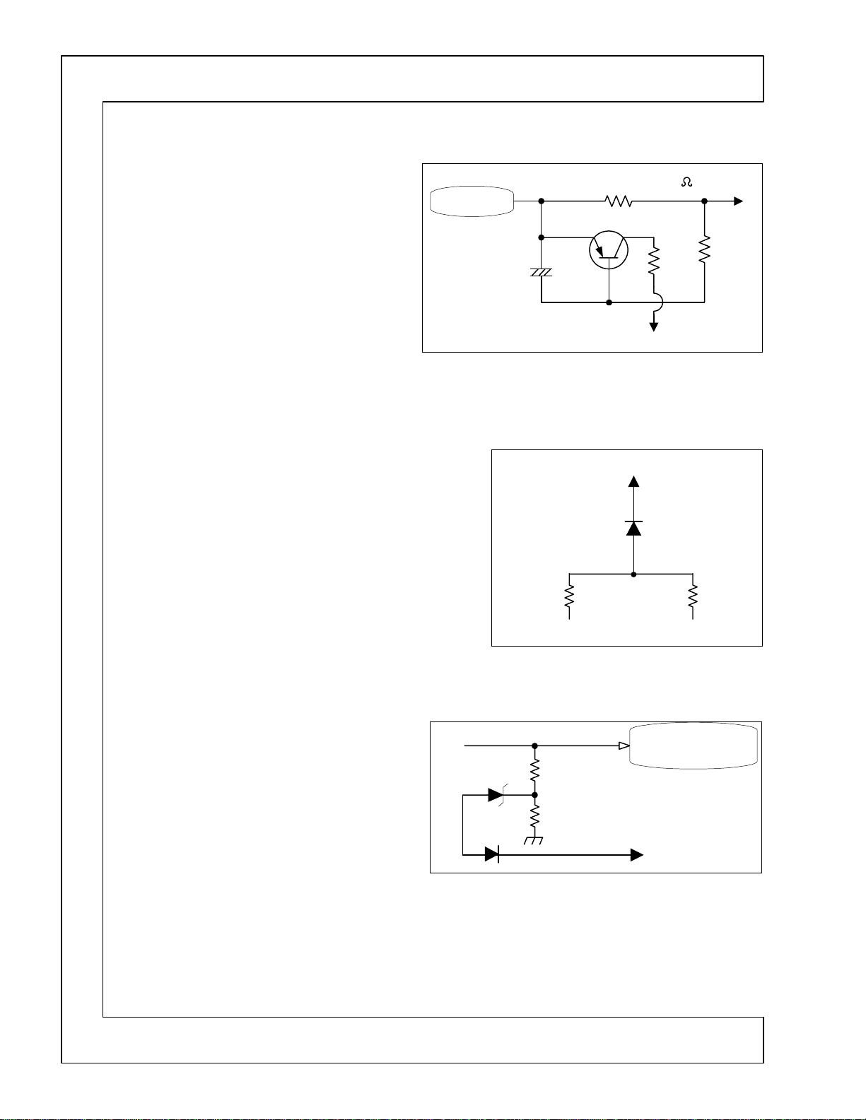
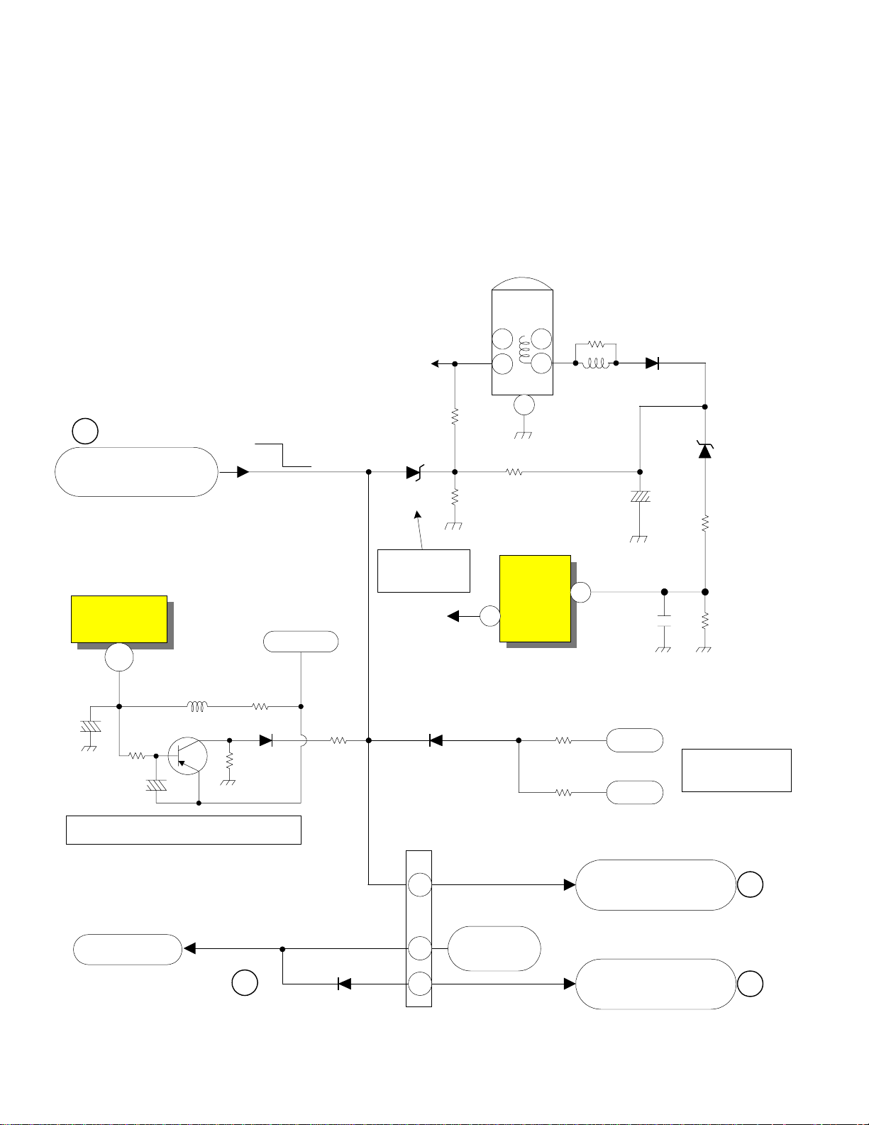
DP-4X GENERIC POWER SUPPLY SHUTDOWN EXPLANATION
GENERIC SHUTDOWN CIRCUITS EXPLAINED:
The following circuits are commonly used in Hitachi product and relate to the drawings for Shutdown:
SW +115V EXCESSIVE CURRENT DETECTION
(See Figure 1)
One very common circuit used in many Hitachi television products is the B+
circuit. In this circuit is a low ohm resistor
ing
in series with the SW +115V. The value of this resistor is
0.39 ohm
creases, the voltage drop across the resistor increases. If the voltage drop is sufficient to reduce the
voltage on the base of
duct, producing a Shutdown signal that is directed to
the appropriate circuits indicated on the drawing for
Deflection Power Supply Shutdown Output Circuit,
OCP & OVP.
NEGATIVE VOLTAGE LOSS DETECTION
(See Figure 2)
The purpose of the Negative Voltage Loss detection circuit is to
compare the negative voltage with its counter part positive voltage. If at any time, the negative voltage drops or disappears, the
circuit will produce a Shutdown signal.
In Figure 2, there are two resistors. One to the positive voltage
+5V and one to the negative voltage –5V. At their tie point,
(neutral point), the voltage is effectually zero (0) volts, actually
about 1 Volt negative. If however, the negative voltage is lost,
the neutral point will go positive. This in turn will create a Shutdown Signal through
dicated on the drawing for Deflection Power Supply Shutdown
Output Circuit, OCP & OVP.
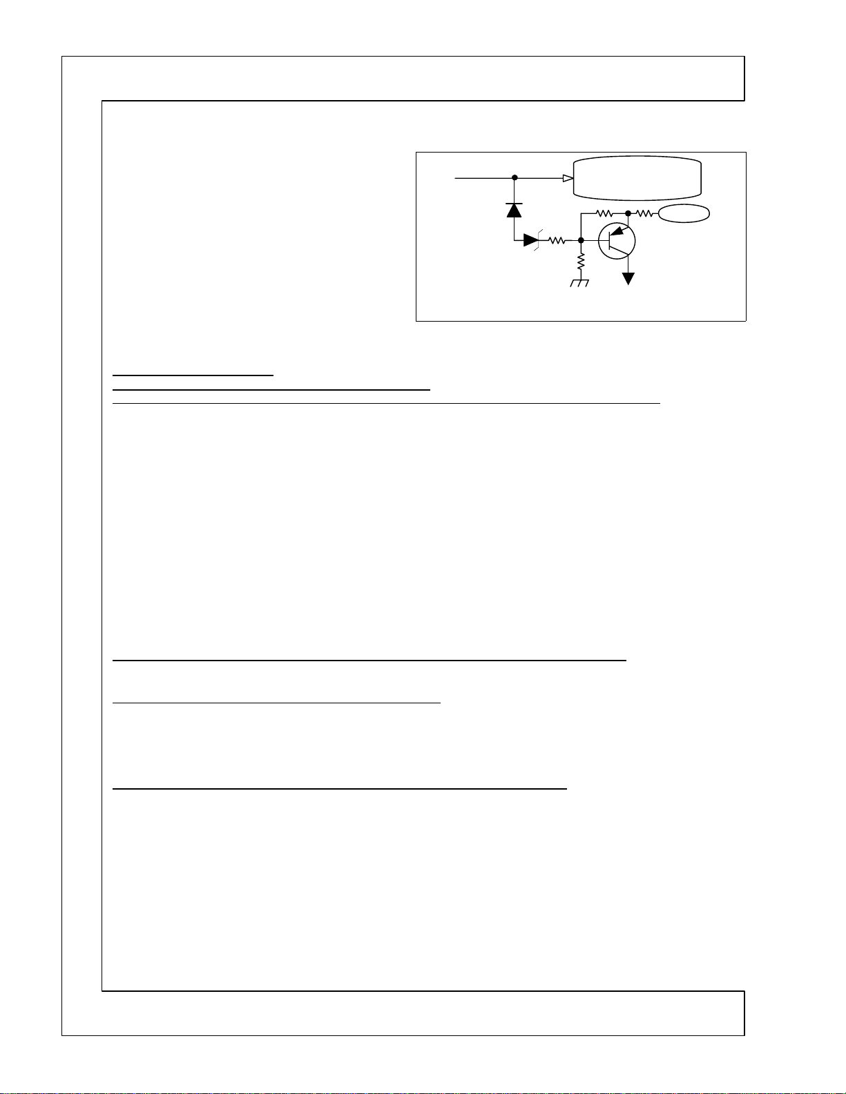
VOLTAGE TOO HIGH DETECTION
(See Figure 3)
Another circuit used is the
circuit. In the example shown in Figure 3, the
tion
zener diode
and
RP38
the voltage at the divider center point will rise as well
and trigger or fire the zener diode which produces a
Shutdown signal through
priate circuit indicated on the drawing for Deflection
Power Supply Shutdown Output Circuit, OCP & OVP.
. When the current demand in-
DP39
. If the voltage source rises too high,
RP39
Excessive Current Sens-
RP34
, the transistor will con-
QP05
and on to the appropriate circuit in-
DK18
Voltage Too High Detec-
is connected to a voltage divider
and on to the appro-
DP38
SW+115V
CP46
Voltage Loss
RK23
2.7K
DP39
DP38
RP34
Current Sensor
QP05
Figure 1
Shutdown Signal
Negative
Detector
SW +5V
RP38
RP39
Figure 3
0.39
RP35
Base
Bias
RP36
Shutdown Signal
DK18
RK22
1.8K
SW -5V
Figure 2
SW +115V
Voltage Too
High Detector
Shutdown
Signal
(Continued on page 6)
PAGE 01-01
Page 8
DP-4X GENERIC POWER SUPPLY SHUTDOWN EXPLANATION
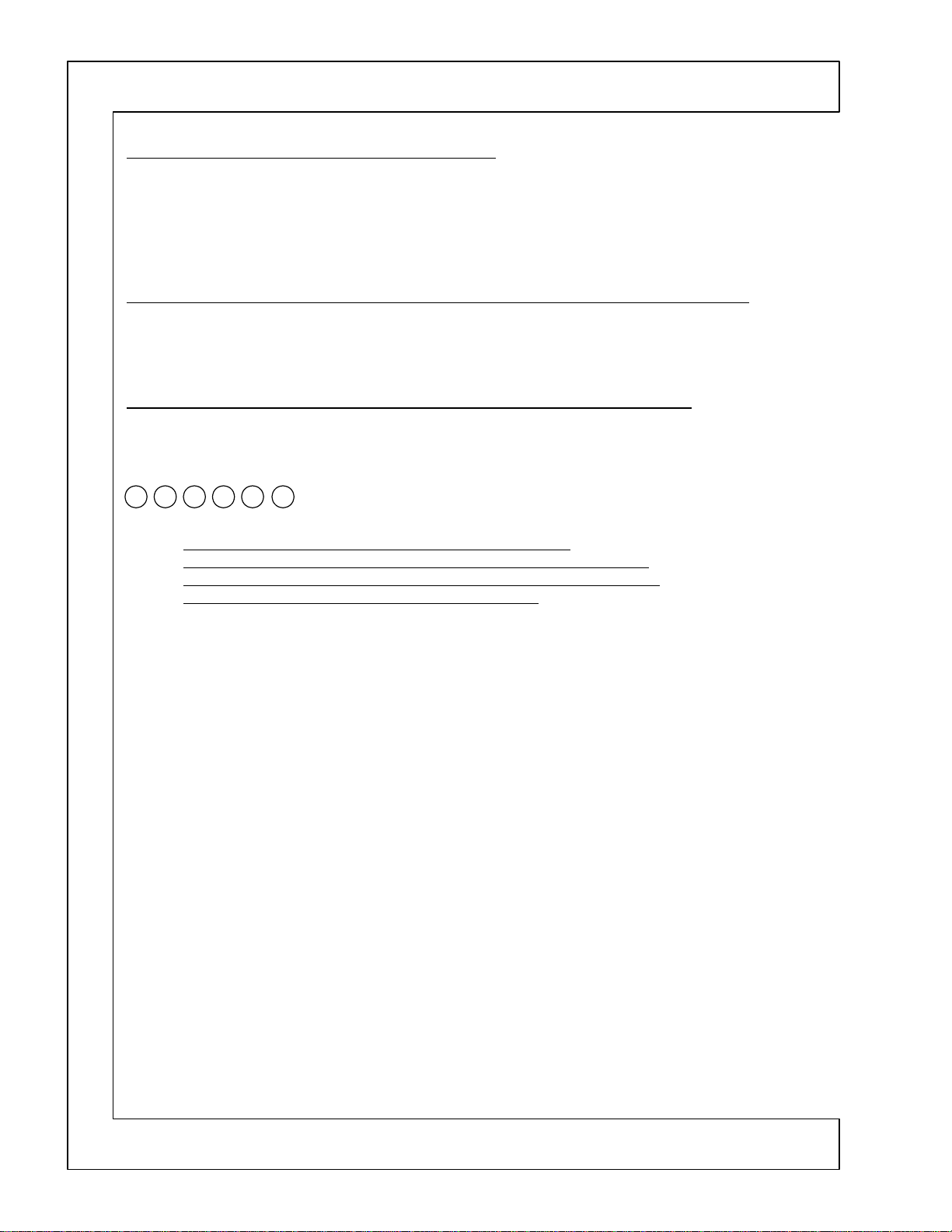
VOLTAGE LOSS or SHORT DETECTION
(See Figure 4)
One circuit used is the Voltage Loss Detection circuit. This is a very simple circuit that detects a loss of
a particular power supply and supplies a Pull-Down
path for the base of a PNP transistor.
This circuit consist of a diode connected by its cathode to a positive B+ power supply. Under normal
Voltage
Loss
Detector
conditions, the diode is reversed biases, which keeps
the base of Q1 pulled up, forcing it OFF. However, if
there is a short or excessive load on the B+ line that’s
being monitored, the diode in effect will have a LOW
on its cathode, turning it ON. This will allow a cur-
Figure 4
Shutdown Signal
rent path for the base bias of Q1, which will turn it
ON and generates a Shutdown Signal.
GENERAL INF O RMATION:
This explains the Overall Power Supply Shutdown Circuits:
Which turns off the Relay Driver for the Deflection Power Supply and the Relay for the Signal Power Supply.
DEFLECTION (High Voltage) POWER SUPPLY:
The Deflecti on Po wer supply is centered around th e Switching Transfor mer TP01 and the driver IC, IP01.
This power supply creates vo ltag es tha t are Swit ched on wh en the Set is turned on.
1. SW +115V 2. +220V
3. +28V 4. SW-28V
5. +7V 6. SW +6.3V
Other supplies are generated from these 6 main voltages.
SIGNAL (Low Voltage) POWER SUPPLY:
The Signal Power supply is centered around the Switching Transformer T201 and the driver IC, I201.
This power supply creates vo ltag es tha t are Swit ched on wh en the Set is turned on.
1. 38.5V or 29V 2. +10.5V
3. +21V 4. SW-5.6V
5. +16V 6. SW +5.7V
Other supplies are generated from these 6 main voltages.
Q204 and Q203 Relay Inhibit Activation. (SHUTDOWN) called COMMON ACTION CIRCUIT.
All Shutdown events will cause the main power relays to turn off. This action will stop all secondary power supplies.
The Low Voltage power supply (Stand-By) will Shutdown along with the Deflection Power Supply.
See the DP-4X Signal Power Supply Sh ut d ow n Circuit for detail s.
If any of the shutdown circuits activate, the base of Q203 will go High. This turn s on Q203 and r emoves the Power On Highs
from PPS1 connector pins 9 (Power_Sig) an d 11 (Power_Def) called Power_1 and Power_3. With this, the main power sup-
plies will STOP . Q204 ope r at es a s a “latch”. Th i s pr e vents Q203 from turning off if the shutdown signal disappears after
shutdown.
SOME SHUTD OW N CIRCUITS ARE DEF E AT ED IN STANDBY M O DE . (Set Off).
When the set is turned off (called Stand By), some of the shutdown inputs are not active because the voltages being monitored
are not on.
• Shorted FAN +10V (from from pin 3 of IC303). This voltage is monitored by D313.
• Stopped Fans PPF2 and PPF3 pin 2. This is monitored by D313.
• Shorted Drv 16.5V (from pin 2 of IC301) This voltage is monitored by D312.
• Prot_Drv (from pin 48 of PPS1) This voltage is monitored by D312.
• Prot_OCP (6 shutdown inputs) This voltage is monitored by D944.
1. SW +2.2V (IV01) * 2. SW +3.3V (IY01) * 3. SW +9V (IY07) *
4. VM +220V (QEA8) * 5. SW +6.3V (QP04) ** 6. SW +28V (DP30) **
* See the PROT_OVP and PROT_OCP Shutdown Diagram.
** See the Deflection Power Supply Shutdown Output Circuit Diagram.
Any Positive
B+ Supply
B+
Q1
(Continued on page 3)
PAGE 01-02
Page 9
DP-4X GENERIC POWER SUPPLY SHUTDOWN EXPLANATION
(Continued from page 2)
See the DP-4X Signal Power Supply Shutdown Circuit for details.
These shutdown circuits are defeated because the SW (Switched) power supplies are turned off in standby. So to prevent
faults triggering of the shutdown circuit, the sensing circuits are turned off also..
Q206
generates the shutdown high signal if any of the shutdown circuits attached to its base become low.
ter voltage to operated.
When the set is turned off,
SHUTDOWN INPUTS EXPLAINED:
GENERAL INFORMATION CONTINUED:
All of the Power Supply Shutdown circuitry can be broken down into the following categories;
Voltage Missing Detection or Short Detection or Negative Voltage Loss Detection
•
Voltage Too High Detection
•
Excessive Current Detection
•
COLD GROUND SIDE SHUTDOWN SENSING CIRCUITS.
All shutdown events arrive at the base of
The shutdown circuit are broken down into four pages. The shutdown outputs from each page are interconnected and indicated by symbols shown below;
A
B C D E F
Please refer to the following Diagrams as you continue to read the following explanations.
The DP-4X Deflection Side Shutdown Diagram for (A), (B), (C), (D).
1.
The DP-4X PROT_OVP and PROT_OCP Shutdown Diagram for (A), (B), (E), (F).
2.
The DP-4X Deflection Power Supply Shutdown Output Circuit Diagram for (C), (D).
3.
The DP-4X Signal Power Supply Shutdown Circuit for (E), (F).
4.
RY05
supplies the 5.7V to the Emitter of
RY05
opens and the 5.7V disappears so
(See previous two pages for generic shutdown circuit details)
Q203
. The shutdown events are categorized in the following pages.
Q206
. This voltage must be active for
Q206
can no longer operate.
(AC must be removed to recover).
Q206
requires emit-
Q206
to function.
:
PAGE 01-03
Page 10
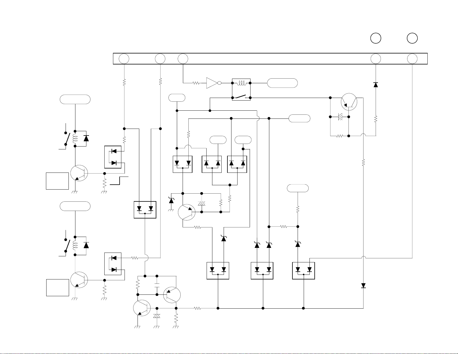
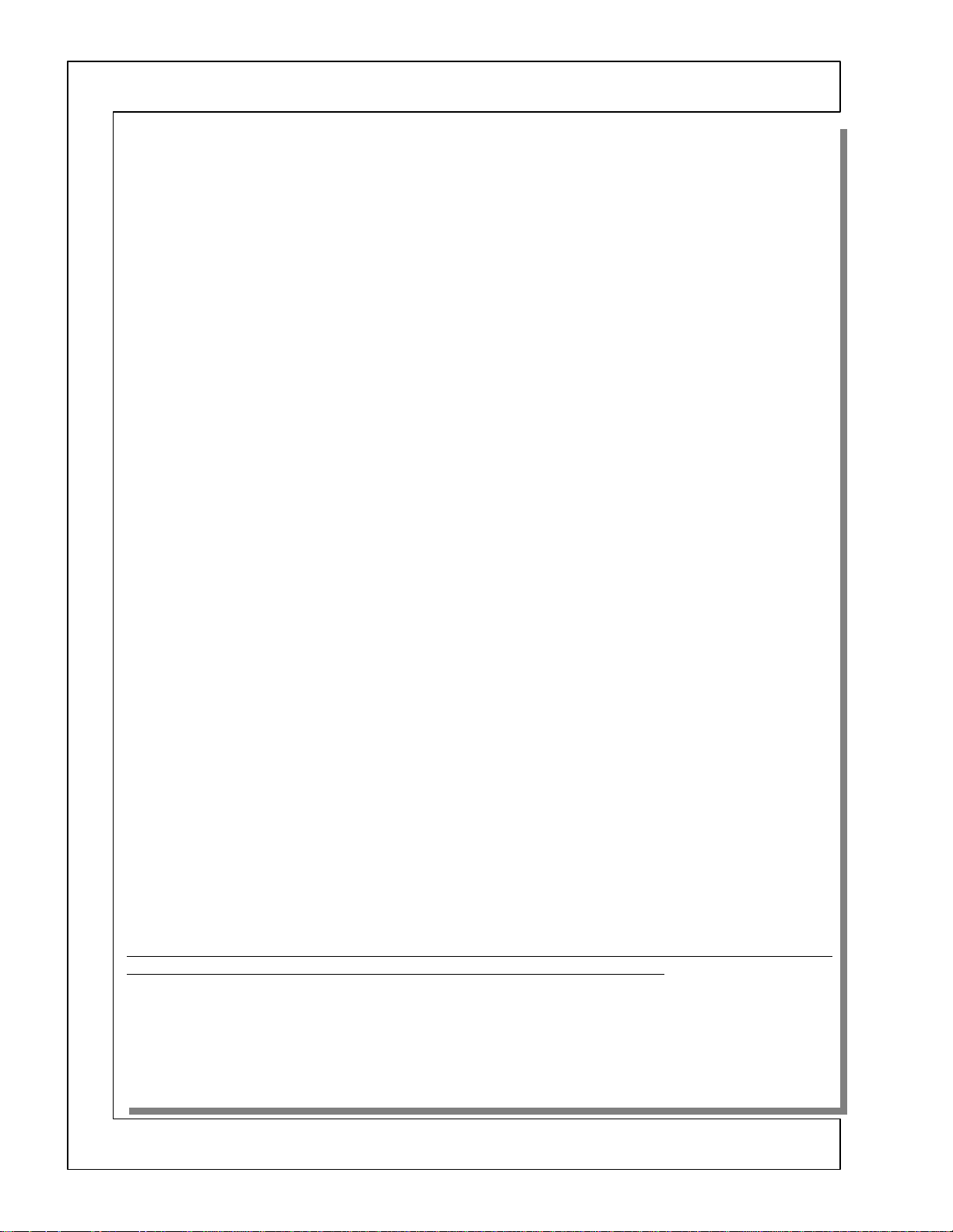
DP-4X DEFLECTION SIDE SHUTDOWN DIAGRAM EXPLANATION
See The DP-4X Deflection Side Shutdown Diagram for (A), (B), (C), (D).
HIGH VOLTAGE TOO HIGH DETECTION: One of the Shutdown circuits for outp ut (A).
•
DH15 High Voltage Too High Sensing Circuit.
This circuit monitors the
. If the voltage created by rectifier
7
zener will fire. This high will be routed to pin 8 of
PROT_OCP Shutdown Diagram
• At the same time, the zener diode
Horizontal Drive for High Voltage and this IC will shut off, turning off High Voltage drive pulses.
• The ABL is tied to the cathode of
as the screen brightness fluctuates and caused the High Voltage to bounce. By tying ABL to the Excessive
High Voltage detection voltage, the firing point is slightly altered.
VERTICAL OUTPUT CI RCUIT EXCESSIVE CURRENT DETECTION: One of the Shutd own circuits for
output (A).
•
Q604 Vertical Circuit Excessive Current Sensing Circuit.
This circuit monitors the
rent,
this transistor. When this happens, its collector will go high. This high will be routed through
pin 8 of
-5V NEGATIVE VOLTAGE LOSS DETECTION: One of the Shutdo wn circuits for output (A).
•
DK18 –5V Loss Detection Circuit.
The purpose of the Negative Voltage Loss detection circuit is to compare the negative voltage with its
counter part positive voltage. If at any time, the negative voltage drops or disappears, the circuit will produce a Shutdown signal.
There are two resistors. One to the positive voltage +5V
RK22
voltage is lost, the neutral point will go positive. This in turn will create a Shutdown Signal through
DK18
Shutdown Diagram.
PROT_OVP INPUT INDICATED BY (C) One of several Shutdown outputs for item (A).
• The
put from the Deflection Power Supply Shutdown Circuit Diagram. There are 3 circuits from the Deflection Power Supply Shutdown Circuit Diagram that provide inputs to this diagram.
• This is explained on Page 01-06.
SW +10.5V SHORT DETEC T INDICATED BY (D) Shutdown output for item (B).
•
D723
age disappears or is shorted,
output as a shutdown signal on the
will develop a larger voltage drop. This will cause the base voltage of
R629
PDS3 PROT_OVP (A)
. At their tie point, (neutral point), the voltage is approxima tely (-1V). If however, the negative
. This high wi l l be routed to pin 8 of
PROT_OVP
is attached to the B+
signal (Active High) is shown in the center left hand side of the diagram. This is an in-
High Voltage
SW+28V
SW +10.5V
D723
line generated by rectifying the pulse from the flyback
and capacitor
DH13
PDS3 PROT_OVP (A)
.
will fire and this high will be routed to pin 7 of
DH14
via
DH15
line going to
to the
PROT_OVP and PROT_OCP Shutdown Diagram.
PDS3 PROT_OVP (A)
line which is generated on the Signal PWB by
cathode will be pulled low generating a Low on Pin 9 of
PROTECT_OCP
. This resistor offers sli ght “Trigger Point” deviations
RH32
Vertical Output IC. If the IC draws too much cur-
I601
indicated as item
at the cathode of
CH17
and one to the negative voltage –5V
RK23
to the
(B)
DH15
to the
Q604
PROT_OVP and PROT_OCP
.
TH01
goes too high, this
PROT_OVP and
. This is the
IH01
to fall turning on
and to
D608
. If this volt-
QY62
and
PDS3
pin
PAGE 01-04
Page 11
DP-4X DEFLECTION SIDE SHUTDOWN DIAGRAM
Any fluctuations in High Voltage will also be
reflected by the 50P output P/P.
By monitoring the 50P (50 Pulse) rises in High Voltage
will be sensed. If High Voltage climbs too high, DH15
will fire and trigger a shut down event.
DH14 will fire and stop High Voltage Horz. Drive
Flyback
RH32 allows ABL fluctuations to
manipulate the Trigger Point of Shut
Down as screen brightness varies.
ABL is inverse proportionate to
brightness.
This prevents false Shut Down triggering.
C
3
Active
PROTECT _OVP
From Deflection Power Supply Shut
Down Output Circuits Diagram.
Vertical Output Circuit
I601
SW 28V
7
R629
C604
L603
Q604
R630
C610
Excessive Vertical Current Det.
0.68 Ohm
D608
R631
Normal
R632
TH01
TH02
8
5OP
4
RH25
Hi Volt
H. Drive
IH01
H. Drive
110
7
OVP
ABL
RH32
DH15
RH24
Excessive Hi
Voltage Det.
1
DK18 Monitors the -5V and +5V lines going to the DCU.
If the -5V line is loss, the +5V line provides the Shut Down Hi.
On the Convergence Circuit Diagram Power Def. page 2 of 3.
High Voltage
Sensing Circuit
RH23
LH06
29.01V
CH17
Stops H. Drive
7
DH13
DH14
RH26
CH10 RH09
+5V
DK18
RK23
2.7K
-5V Loss Det.
-5V
RK22
PDS3
1.8K
If the Vertical Output IC has a problem, R629
will sense the current rise. The voltage drop will
be reflected at the base of Q604 turning it on
and producing a Shut Down high.
SW +10.5V
D723
D
SW +10.5V From QY62 SW +10.5V Regulator on Signal 5 of 5 Schematic.
8
10
9
SW
+10.5V
6
1
PROTECT _OVP
To Signal PWB
See Protect_OVP and Protect_OCP
Shut Down Diagram for Details.
PROTECT _OCP
To Signal PWB
PAGE 01-05
A
B
Page 12

DP-4X PROT_OVP and PROT_OCP SHUTDOWN DIAGRAM EXPLANATION
PROT_OVP and PROT_OCP SHUTDOWN CIRCUITS EXPLAINED: (A) (B) (E) (F)
(See the PROT_OVP and PROT_OCP Shutdown Diagram for Details).
CPT PROTECT (+200V Excessive Current Detection):
•
On the RED CRT PWB +220V (VM 200V) Excessive Current Detection
Monitored by
The collector will go high. This high will go to the connector
high continues to the Green CRT PWB connector
and
CPT PROTECT
• This line is connected to the
Circuit, identified as
• Any High from this line is then routed to the
is routed to the Signal Power Supply Shutdown Circuit Diagram identified as
VM GAIN CONTROL (VM 200V Excessive Current Detection):
•
On the BLUE CRT PWB VM+220V Excessive Current Detectio n
Monitored by
it on.
The collector will go high. This high will go to the connector
high continues to the Green CRT PWB connector
• This line is connected to the
• This line is also connected to the base of
High to a Low on its collector.
• The collector of
and the
PROT_OCP (B)
VOLTAGE LOSS DETECTION CIRCUITS:
•
•
•
•
PROT_OCP
generates the SW +2.5V. If this line is shorted or missing, this line will drop Low.
IV01
generates the SW +3.3V.
IY01
missing, the cathode of
generates the SW +9V.
IY07
ing, the cathode of
PROT_OCP: LABELED AS OUTPUT (F).
Any low from this line is then routed to the
. From here this low is routed to the Signal Power Supply Shutdown Circuit Diagram and
(F)
again identified as
. If the
RE35
on the Signal PWB.
6 inputs active High.
(A)
. If the
REF1
is tied to several circuits. The
QY60
from the Deflection Side Shutdown Circuit from
which represents 1 shut down input from the Deflection Side Shutdown circuits.
DY04
draws too much current, the base voltage of
220V
connector which ties the inputs from the Deflection Side Shutdown
PDS3
VM220V
VM Signal
DY03
goes low which pulls the
(F)
draws too much current, the base voltage of
generation circuit and turns it off.
QY60
One of several Shutdown outputs for (F).
is connected to the SW +3.3V line. If this line is shorted or
DY03
goes low which pulls the
is connected to the SW +9V line. If this line is shorted or miss-
DY04
.
One of several Shutdown outputs for (E).
will fall turning it on.
QE08
pin 7 labeled as
ERG1
pin 3 labeled
PSC
connector pin
PPS1
One of several Shutdown outputs for (F).
EGB1
pin 2 labeled
PSC
. This transistor acts as an inverter to change the output
Voltage Loss Detection Circuits
PROT_OCP
PROT_OCP
connector pin
PPS1
VM PROT
identified as
47
pin 8 labeled
VM GAIN
PDS3
line low.
line low.
45
connector pin 9. Labeled as
identified as
VM PROT
on the Green CRT PWB
. From here thi s high
(E)
.
(E)
QEA8
GAIN CONT
.
will fall turning
explained below
PROT_OCP
. This
. This
PAGE 01-06
Page 13
DP-4X PROT_OVP and PROT_OCP SHUTDOWN DIAGRAM
PROT_OVP SHUT DOWN DIAGRAM
+220V
VM
220V
PDC1
EGB2
2
QEA8
1
RE35
2.2 Ohm
QE08
CE10
REF1
10 Ohm
REF2
REE9
SW +2.2V Reg
RED CRT PWB
R.G.B. Drives
RE27
RE31
VM 200V
RE34
VM PROT
ERG1
7
GREEN
CRT
PWB
PSC
VM PROT
SIGNAL PWB
3
CPT
PROTECT
RE29
Text Indicates the Labels on the Schematic
PROT_OCP SHUT DOWN DIAGRAM
BLUE CRT PWB
VM Circuit
REF4
REF5
CEC1
SIGNAL PWB 2 of 3
DEB6
REF5
CONT
GAIN
EGB1
8
GREEN
CRT
PWB
PSC
VM GAIN
CONT
Also Shuts Off
VM Signal
Generation Circuit
2
1
Active Hi
VM GAIN
CONT
DEF. PWB /
DEF. POWER
PDS3PDS3
6
8
PROT_OVP
From Deflection
Side Shut Down
Circuit
Active Hi
PROT_OVP
7
5
PROT_OCP
Active Lo
A
PPS1
47
45
SIG
POWER
PWB
See Signal
Power Supply
Shut Down
Circuit
E
F
SW +5.7V
DM +10.5V
IV01
1
3 8
SW +3.3V Reg
IY01
1
SW +9V Reg
IY07
7
SW +2.5V
DEF. PWB /
DEF. POWER
PDS3
CZ04
3
SW +3.3V
DY03
RZ62
4
RL50
QY60
RZ60
35
SW +9V
DY04
3
RZHD
1
9
B
PROT_OCP
From Deflection
Side Shut Down
Circuit
SIGNAL PWB
PAGE 01-07
Page 14

DP-4X DEFLECTION POWER SUPPLY SHUTDOWN OUTPUT DIAGRAM EXPLANATION
DEFLECTION POWER SUPPLY SHUTDOWN OUTPUT CIRCUIT DIAGRAM EXPLAINED: (C)
(See the Deflection Power Supply Shutdown Output Circuit Diagram for Details).
PROT_OVP: Identified as (C).
EXCESSIVE DEFLECTION 115V B+ CURRENT DETECTION: Part of several Shutdown outputs to (C).
•
•
•
•
EXCESSIVE DEFLECTION 115V B+ VOLTAGE DETECTION: Part of several Shutdown outputs to (C).
•
•
•
SW -28 VOLT SHORTED or MISSING DETECTION: Part of several Shutdown outputs to (C).
•
•
monitors
QP05
enough to turn on
ing an increase in the voltage drop across this resistor. If there is enough current the base voltage of
will drop enough to turn on t his transistor . When
fire zener diode
and
CP49
out and fluctuations on the anode of
DP37
and identified as
PROT_OVP
DP39
Deflection
DP37
and identified as
PROT_OVP
identified as
SW -28V Shorted or Missing Detection
Monitored by
zener to fire. This high will be routed through
PROT_OVP
PROT_OVP
identified as
RP37
cathode is connected the anode of
is routed to the Deflection Side Power Supply Shutdown Diagram also identified as
monitors the Deflection
115V B+
cathode is connected the anode of
Identified as
(C)
DP46
and identified as
Identified as
(C)
current draw.
RP34
. However, if there is a problem, the current draw through
QP05
and generate a high on the anode of
DP36
prevent faults triggering of the shut down line due to High Voltage bounce by smoothing
.
(C)
115V B+
line goes to o high,
.
(C)
is routed to the Deflection Side Power Supply Shutdown Diagram also
(C)
.
. If the
SW-28V
.
(C)
is routed to the Deflection Side Power Supply Shutdown Diagram also
(C)
.
is a 0.39 low ohm resistor. Normally the current draw isn’t
RP34
increases caus-
RP34
turns on, its collector goes high. This high will
QP05
DP37.
.
DP36
. This line is connected to the line labeled
DP38
line via the Voltage divider consisting of
will fire and generate a high on the anode of
DP39
. This line is connected to the line labeled
DP38
is shorted or missing, the cathode will be pulled high causing the
. This line is connected to the line labeled
DP47
RP38
PROT_OVP
and
RP39
.
DP37
PROT_OVP
QP05
(C)
. If the
.
PAGE 01-08
Page 15
TP01
DP-4X CHASSIS
Deflection Power Supply Shutdown Output Circuit Diagram
OCP and OVP
+28V
-28V
16
15
14
DP30
CP30
CP32
CP33
DP31
CP31
+
+
CP49
RP37
LP30
LP31
LP33
RP46
+
CP34
DP50
+
CP35
RP47
DP37
DP36
GREEN
L.E.D.
-28V Short or Loss Detection
DP46 DP47
LP34
DP38
1.26A
0.65A
SW -28V
Active High
3
PROT_OVP
C
To Deflection Side
Power Supply Shut
Down Diagram
SW+ 28V
10
11
11
18
17
CP39
+115V
2
DP34
14
3
CP45
CP46
+7V
2
DP32
14
3
CP36
DP48DP49
0.39 Ohm
+115V Over Current
Detection
QP04
RP34
RP36
QP05
RP35
0.19A
0.69A
EP02
2 Amp
RP38
DP39
RP39
DP40
SW + 7V
SW + 6.3V
LP37
GREEN L.E.D.
SW + 115V
0.85A
+115V Over Voltage
Detection
PAGE 01-09
Page 16
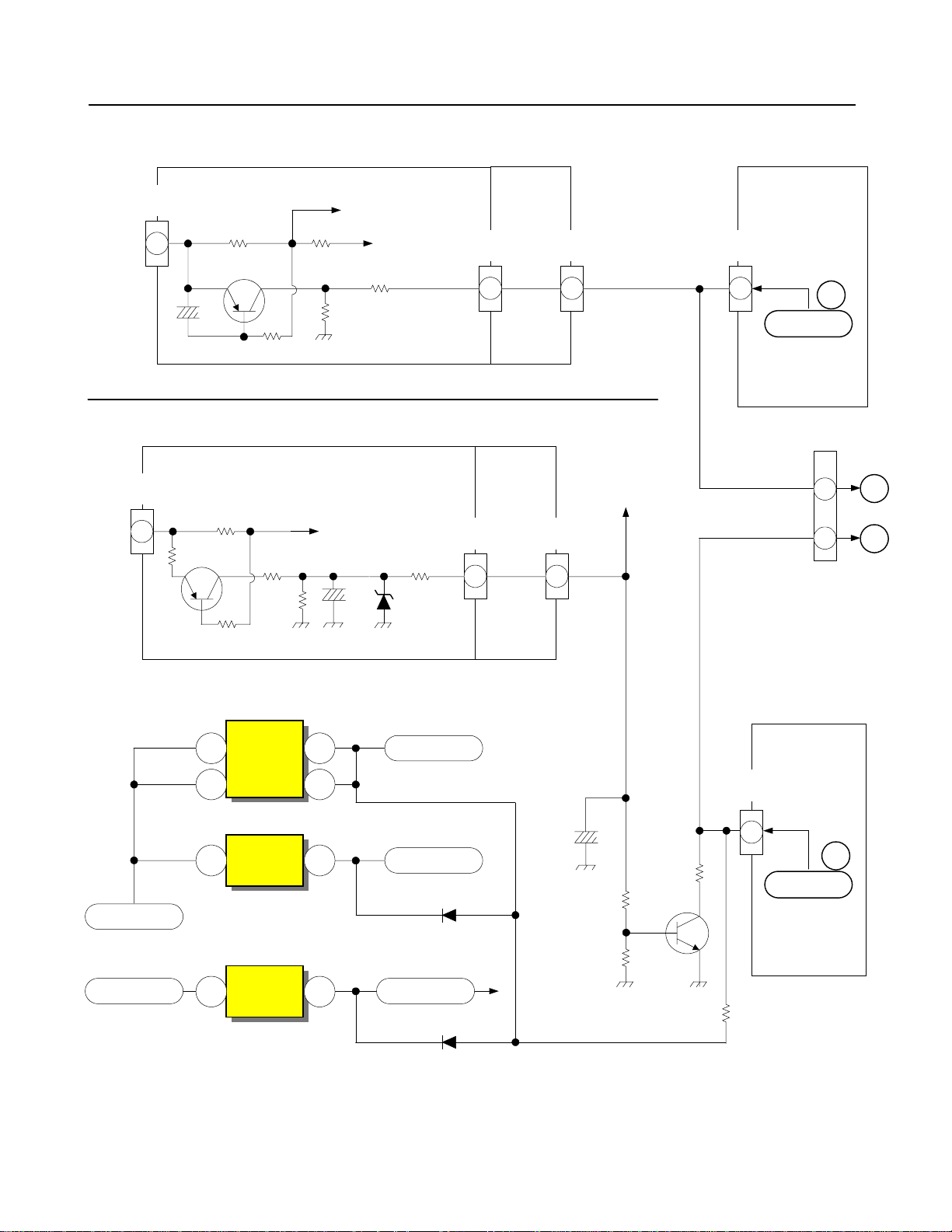
DP-4X SIGNAL POWER SUPPLY SHUTDOWN CIRCUIT EXPLANATION
See the DP-4X Signal Power Supply Shutdown Circuit for details. This includes inputs (E) and (F).
There are a total of 20 individual Shutdown inputs to the Relay Inhibit transistor Q203 shown on the Signal
Power Supply Shutdown Circuit.
• There are 8 individual Shutdown detection circuits on the Signal Power Supply Circuit Diagram.
• There are a total of 5 individual Shutdown inputs from the Deflection PWB via PROT_OCP (active
Low). Input from the PPS1 connector pin 45
• There are a total of 7 shutdown inputs from PROT_OVP (active High) input from the PPS1 connector
pin 47.
SHUTDOWN INPUTS EXPLAINED:
Q204 and Q203 Relay Inhibit Activation. (SHUTDOWN) called COMMON ACTION CIRCUIT.
All Shutdown events will cause the main power relays to turn off. This action will stop all secondary power
supplies. The Low Voltage Signal Power Supply will Shutdown along with the Deflection Power Supply.
• Q203 CIRCUIT EXPLAINED:
• If any of the shutdown circuits activate, the base of Q203 will go High. This turns on Q203 and removes
the Power On Highs from PPS1 connector pins 9 (Power_Sig) and 11 (Power_Def) called Power_1 and
Power_3. With this, the main power supplies will STOP. Q204 operates as a “latch”. This prevents
Q203 from turning off if the shutdown signal disappears after shutdown.
POWER ON/OFF RELAYS RY101 and RY102:
RY101 Explained:
• The Relay RY101 supplies AC to the Signal Power Supply bridge rectifier DS201. When this relay en-
gages, the Signal Power Supply starts up and supplies the voltages mentioned below.
SIGNAL (Low Voltage) POWER SUPPLY:
• The Signal Power supply is centered around the Switching Transformer T201 and the driver IC, IP01.
• This power supply creates voltages that are Switched on when the Set is turned on.
1. 38.5V or 29V 2. +10.5V 3. +21V
4. SW-5.6V 5. +16V 6. SW +5.7V
• Other supplies are generated from these 6 main voltages.
RY102 Explained:
• The Relay RY102 supplies AC to the Deflection Power Supply bridge rectifier DP01. When this relay
engages, the Deflection Power Supply starts up and supplies the voltages mentioned below.
DEFLECTION (High Voltage) POWER SUPPLY:
• The Deflection Power supply is cente r ed arou nd the Switching Transf o r me r TP01 and the driver IC, IC201.
• This power supply creates voltages that are Switched on when the Set is turned on.
1. SW +115V 2. +220V 3. +28V
4. SW-28V 5. +7V 6. SW +6.3V
• Other supplies are generated from these 6 main voltages.
CIRCUITS ATTACHED TO THE BASE OF Q203:
This year, Hitachi is utilizing a three legged diode OR gate style of input device for feeding shutdown inputs
to the base of Q203. These diode OR gates and circuits attached are explained next.
(Continued on page 11)
PAGE 01-10
Page 17

DP-4X SIGNAL POWER SUPPLY SHUTDOWN CIRCUIT EXPLANATION
(Continued from page 10)
D214 Left Hand Input Circuits:
The left hand input to
base inputs a re monitoring DC voltages for short s .
Q205 base input circuits.
•
•
The Emitter of
right hand i nput is
these voltages without fail. If either the
D214 Right Hand Input Circuit:
The right hand input to
over voltage condition. If this voltage rises too much, the zener will fire generating a high on its anode and
through
D217 input circuits.
•
D217 Left Hand Input:
1.
•
D217 Right Hand Input:
1.
D218 input circuits.
•
D218 Left Hand Input:
1.
•
D218 Right Hand Input:
1. This monitors the
D220 input circuits.
The anode of diode
input is monitoring the
inputs will be Low in nature. There are a total of 5 inputs fed to this pin described in the previous 9 pages.
• See references to (F) on the PROT_OVP and PROT_OCP SHUTDOWN DIAGRAM.
D115:
1. The left hand input monitors the 5.7V line for shorts.
2. The right hand input monitors the 35V line for shorts.
D116:
1. The left hand input monitors the 10.5V line for shorts.
2. The right hand input monitors the 3.3V line for shorts.
Q205
10.5V
to the
D214
ZD202
much, the zener will fire generating a high on its anode and through
Circuit
ZD203
much, the zener will fire generating a high on its anode and through
Circuit
ZD205
tive voltage fed through R241 will pull the cathode of zener diode
generating a high on its anode and through
total of 7 inputs fed to this pin described in the previous 9 pages. If this voltage goes high, the high
will be dir ected through
Common Action Circuit
. This monitors the DC voltage
.
. This monitors the DC voltage
.
. This monitors the DC voltage -
• See references to (E) on the PROT_OVP and PROT_OCP SHUTDOWN DIAGRAM.
D220
is connected to the collector of
D214
pull up voltage is supplied through
. This assures the emitter voltage is always present and allows
or the
10.5V
is connected to the anode of
D214
.
5.7V
10.5V
5.6V
PROT_OVP
is connected to the collector of
PROT_OCP
inputs also labeled as
to the
D218
inputs also identified as
Common Action Circuit
D213
3.3V
for an over voltage condition. If this voltage rises too
for an over voltage condition. If this voltage rises too
for a loss or short. If this voltage disappears, the posi-
D218
Q206
. This transistor works as an inverter. Its
Q205
. The left hand input to
line is shorted, this transistor will still function.
. This monitors the DC voltage 3.3V for an
ZD204
D217
D217
ZD205
to the
Common Action Circuit
to the connector
(E)
.
. This transistor works a s a n inverter. Its base
from the connector
(F)
is
D213
Q205
to the
Common Action
to the
Common Action
high. The zener will fire
.
pin 47. There are a
PPS1
pin 45. These
PPS1
and the
5.7V
to monitor
PAGE 01-11
Page 18
DP-4X SIGNAL POWER SUPPLY SHUTDOWN CIRCUIT
Power 1
Power 3
Power 2
PPS1
EF
PROT_OVPPROT_OCP
For
Signal
Power
Supply
DS201
Relay
Driver
For
Deflection
Power
Supply
DP01
AC
Q101
AC
SBY +5V
RY101
SBY +5V
RY102
D104
D109
R118
D105
R110
D110
9
onoff
D111
R122
11
R125R120
5.7V
12
R126
R236
Q104
35V 3.3V
RY105
SBY +5V
10.5V
Q206
C232
R238
45 47
5
Active Low Active High
D219
R237
R239
7
D213 D115 D116
ZD206
C237
R224
R235
-5.6V
R240
Q205
R233
ZD204
ZD202
R241
ZD203
ZD205
PAGE 01-12
Relay
Driver
Q102
R121
R230
Q203
C235
C238
Q204
R231
R232
D214 D217 D218
20
D220
5825
Page 19
DP-4X STAND BY +5V POWER SUPPLY GENERATION EXPLANATION
STAND-BY +5V POWER SUPPLY GENERATION EXPLANATION:
The Stand By power supply operates anytime the set is plugged into an AC outlet. Shown
below in Figure 1 is the Stand By power supply.
a self contained Oscillator, Driver IC. It switches the primary of
The secondary of
the voltage is clamped by
T101
produces the SBY +5V via the rectifier
ZD101
.
A feedback to
IC101
is supplied by the photo coupler
IC102
•
IC102
works as a variable resistor attached to the cathode of the internal LED inside
. As the
SBY +5V
changes so will the resistance of
tance goes Down. As the Resistance goes down the Light emitted from the LED will increase. As the Light increases from the LED, the receiver will conduct more heavily.
This decreases the voltage fed back to
to reduce the primary switching of
IC101
T101
IC101
is the Driver IC for this supply. It’s
T101
.
D103
and filter
PC102
for regulation purposes.
IC102
. Voltage Up, Resis-
causing the internal circuits within
and reduce the
SBY 5.7V
line back to normal.
C106
. Then
IC101
L102
F103
DS101
-+
C105
IC101
D102
C110C107
C106R110
T101
PC102
IC102
D103
C106
R112
SBY +5V
ZD101
R111
R113
C109
R114
R115
Figure 1
PAGE 01-13
Page 20

DP-4X POWER SUPPLY RELAY CONTROL EXPLANATION
See The DP-4X Stand By +5.7V Generation Circuit Explanation for details.
See The DP-4X Power On and Off Circuit Diagram for details.
Power Supply On and Off Circuit Explanation:
The DP-4X Chassis utilizes 5 relays.
RY101
1.
RY102
2.
RY103
3.
RY104
4.
RY105
5.
RY104
(4)
Starting with
supplies AC to the Bridge Rectifiers for the Signal and Deflection Power Supplies.
When The Stand By Power Supply develops the
voltage is delivered to the primary windings of
RY104
RY101
(1)
When the set is turned on, the
croprocessor
high is sent to
From here this high goes to the Deflection PWB through
Q101
of
coil inside
DS201
fier
RY102
(2)
When the set is turned on, the
croprocessor
high is sent to
From here this high goes to the Deflection PWB through
Q102
of
turn for the coil inside
Then to the Deflection Power Supply rectifier
gins to operate.
RY103
(3)
When the set is turned on, the
croprocessor
labeled
Base of
ground return for the coil inside
connector
on to the Audio Output IC
AC Supply to the Signal Power Supply Relay
AC Supply to the Deflection Power Supply Relay
DC Supply to the Audio Output Relay
AC Supply to all AC Relays Relay
DC (SW +5.7V) Supply to the Low Voltage Regulators Relay
AC Supply to all AC Relays Relay
RY104
. This turns on the relay and supplies AC to the above mentioned circuits.
AC Supply to the Signal Power Supply Relay
I004
Q018
goes high and the transistor turns on. This action supplies a ground return for the
RY101
and the Signal Power Supply begins to operate.
AC Supply to the Deflection Power Supply Relay
I004
Q023
. The base goes high and the transistor turns on. This action supplies a ground re-
DC Supply to the Audio Output Relay
I004
POWER 2
Q103
. The Base goes high and the transistor turns on. This action supplies a
PPS1
because this Relay supplies AC to
POWER SIG
. (This high also turns on the Power LED on the front of the set). This
Q021
and
and the relay turns on supplying AC to the Signal Power Supply recti-
. (This high also turns on the Power LED on the front of the set). This
and
RY102
. This high is sent to
. From here this high goes to the Deflection PWB through
pins 1,
2
then to the
POWER DEF
Q024
then to the
and the relay turns on supplying AC to the connector
POWER DM
RY103
and 3. Then to the Signal PWB and
IA02
.
SBY +5V
RY104
command is supplied from pin 59 of the Mi-
PPS1
connector pin 9 labeled
command is supplied from pin 58 of the Mi-
PPS1
connector pin
DP01
command is supplied from pin 91 of the Mi-
Q028
and the relay turns on supplying Audio B+ to the
and
Q029
(Page 01-16)
RY101
and to the relay driver Q105 for
R120, R110, D109
R125, R122, D110
and the Deflection Power Supply be-
then to the
and
, (see previous page) this DC
11
(Previous Page)
RY102
labeled
PPS1
Continued on Next Page
which in turn
POWER 1
to the Base
POWER 3
to the Base
connector pin
R124
.
.
PC2.
to the
12
PAGE 01-14
Page 21

DP-4X POWER SUPPLY RELAY CONTROL EXPLANATION
Continued from Previous Page
See The DP-4X Power On and Off Circuit Diagram for details. (Page 01-16)
RY105
(5)
DC (SW +5.7V) Supply to the Low Voltage Regulators Relay
When the set is turned on, the
Microprocessor
I004
. This high is sent to
pin 12. From here this high goes to the Deflection PWB through
Q104
. The Base goes high and the transistor turns on. This action supplies a ground
return for the coil inside
nector
PPS1
pins 25,
26
POWER DM
RY105
27.
and
command is supplied from pin
Q028
and
Q029
then to the
R126
and the relay turns on supplying
SW 5.7V
Then to the Signal PWB and on to the following Low
Voltage Regulators and ICs.
•
SIGNAL 5 of 5 DIAGRAM (AV Selector).
IY01 +
◊
IY02 +
◊
IY08
◊
•
SIGNAL 4 of 5 DIAGRAM (3D Y/C)
IV01 +
◊
•
SIGNAL 1 of 5 DIAGRAM (Micro).
I010
◊
I013
◊
I006
◊
I008
◊
3.3V Regulator.
5V Regulator.
SW +5V Regulator.
2.5V Regulator.
Bus Select Switch.
+3.3V Regulator.
AV Control IC
IR Blaster Select Switch.
91
of the
PPS1
connector
to the Base of
to the con-
PAGE 01-15
Page 22
DP-4X POWER ON and OFF CIRCUIT DIAGRAM
Audio 38.5V or 29V
SW +5.7V
For Signal
Power Supply
AC
Relay
Driver
SBY +5V
AC to
DS201
Q101
RY101
PPS1
D104
D109
R118
R120
R110
9
onoff
POWER 1
For Deflection
Power Supply
AC
Driver
Relay
AC to
PC2
Q102
RY102
R125
11
38V
531
12
POWER 3 POWER 2
RY103
For
D105
D110
R121
R122
onoff
Audio
Outputs
Q103
Relay
Driver
D106
R124
R123
R126
R127
28 27 25
5.7V
RY105
D108
5.7V38V
Q104
Relay
Driver
Microprocessor
PAGE 01-16
POWER LED
I004
POWER SIG
POWER DM
POWER DEF
SW +10.5V
59
91
58
Signal PWB
Q018 Q021
Q028 Q029
Q023 Q024
QY63
QY62
PPS1
9
12
11
PDS3
10
POWER 1
POWER 2
POWER 3
Signal Power Supply PWB
ZD102
R126
R125
D107
RY104
For Signal and
Deflection Power
Supply
AC Relays.
AC
Q105
Relay
Driver
Page 23

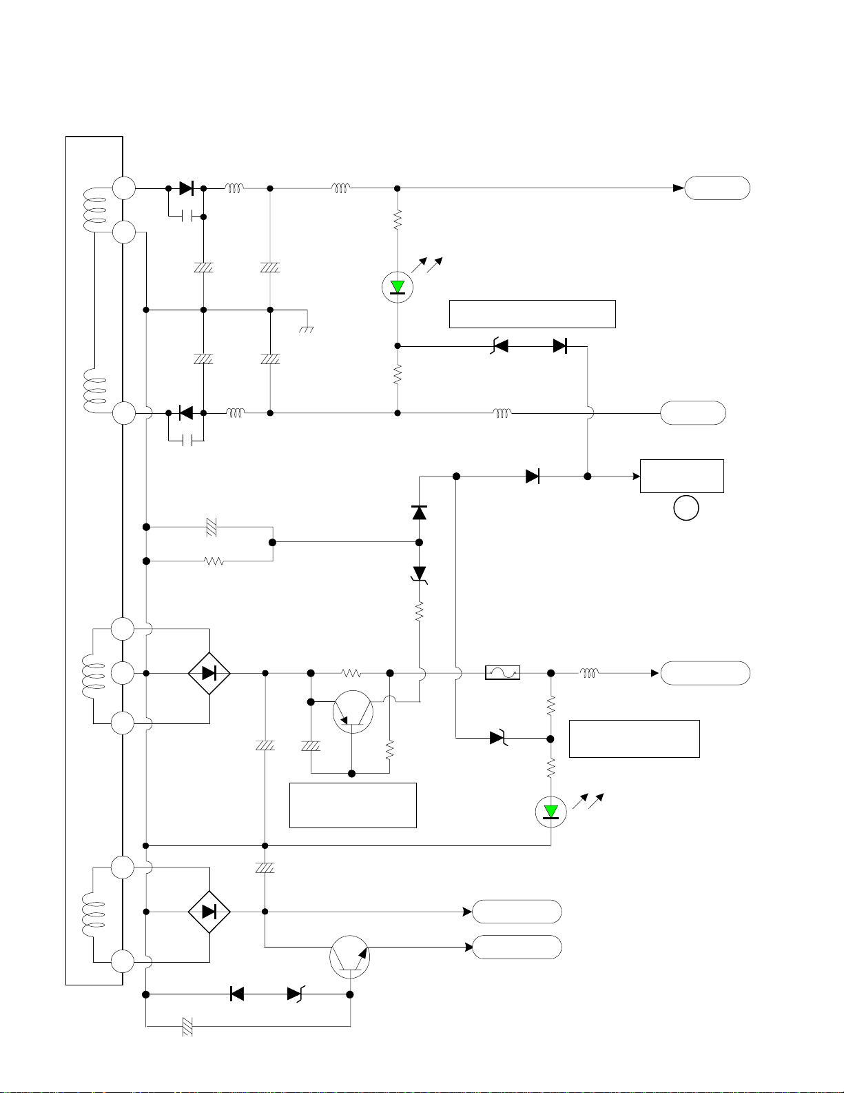
DP-4X POWER SUPPLY SW +115V REGULATION EXPLANATION
Hi-Voltage Power Supply Regulation Circuit Diagram explanation:
(See Power Supply SW+115V Regulation Circuit Diagram for details)
THIS POWER SUPPLY RUNS ONLY WHEN THE SET IS TURNED ON:
TURNING ON THE SW +115V POWER SUPPLY
RY102 AC Supply to the Deflection Power Supply Relay
When the set is turned on, the POWER DEF command is supplied from pin 58 of the Microprocessor I004.
(This high also turns on the Power LED on the front of the set). This high is sent to Q023 and Q024 then to the
PPS1 connector pin 11 labeled POWER 3. From here this high goes to the Deflection PWB through R125,
R122, D110 to the Base of Q102. The base goes high and the transistor turns on. This action supplies a ground
return for the coil inside RY102 and the relay turns on supplying AC to the connector PC2. Then to the Deflec-
tion Power Supply rectifier DP01 and the Deflection Power Supply begins to operate.
DP01 develops raw 300V via the doubler circuit comprised by CP03 and CP04. This voltage is routed through
FP01 to the Drain of QP01. A sample of this DC is routed through RP03 as Start Up voltage for IP01 at around
309V. From the Source of QP01 (when switched) the pulsed DC is routed to pin 9 of TP01. This voltage is
routed through the primary coil inside TP01 and out pins 7. One path from here is sent to pin 9 of IP01 which is
the Over Current Detection pin. The Ground return path for the primary voltage is routed through three 0.22 ohm
resistors R911, R912 and R913.
The Source of QP01 is also connected to the Drain of QP02. In this way, QP01 acts to connect raw B+ to the
primary of TP01 during the field build up period and QP02 acts as a ground switch during the collapse of the
primary field. QP01 gate control is via pin 16 of IP01.
After the Deflection Power Supply begins to operate, IP01 needs Run Voltage. This is accomplished by the pulse
from TP01 pin 5 being rectified by DP04, filtered by CP13 and the DC component arrives at pin 8 of IP01.
SW +115 REGULATION
SW +115V pulse is generated from pin 10 and 11 of T901. This pulse is rectified by DP34, filtered by CP45 and
then routed through the Excessive Current sensing circuit RP34 and QP05.
The primary route for the SW +115V is through EP02, LP37 and output as SW +115V to the Deflection and
High Voltage generation circuit.
However, the regulation route is to pin 1 of IP03. Internally, the regulator circuit works as a variable resistor
whose resistance is dependant upon the SW +115V voltage fluctuations. The internal variable resistor manipulates the current flow from pin 6 to pin 7 ground. This will cause the voltage at pin 2 of IP02 to be controlled.
Internally, the LED is illuminated by degrees dependant upon the SW +115V voltage fluctuations. The internal
receiver receives this light and acts as a variable resistor from pin 4 which is the regulation control signal to pin 3
hot ground.
This action causes pin 2 of IP01 to manipulate the internal oscillator within IP01. This in turn causes the timing
of the drive pulses delivered to the Gate of QP01 and QP02 SMOSFET (Switch Metal Oxide Semiconductor
Field Effect Transistor) to manipulate the frequency of the pulse generated on the primary of TP01. The current
drain of these SMOSFETs is monitored by three low ohm resistors mentioned above. If this current exceeds a
specific value, the voltage developed by these low ohm resistors is routed through RP14 ba ck into pin 9 of IP01
which is the Over Current Protection circuit. This pin will inhibit the drive signal to the ga te of the SMO SFETs.
As soon as the excessive current situation is eliminated, the IC will recover and continue functioning.
B+ GENERATION FOR THE POWER SUPPLY DRIVER IC:
Vcc for the Driver IC is first generated by the AC input. This voltage is called Start Up Voltage. IP01 requires
23.3V DC to operate normal. However, it will begin operation at a much smaller voltage on pin 18.
When AC is applied to the main full wave bridge rectifier DP01 where it is converted to Raw 300V DC voltage,
voltage doubler filter CP03 and CP04, routed through RP03 and made available to pin 18 of IP01 as start up
voltage. This voltage climbs to 300Vdc and the internal Regulator of IP01 is turned On and begins operation.
When the power supply begins to operate, the magnet field collapses and the EMF is coupled over to the secondary windings, as well as the drive windings. The drive windings at pin (5) produce a run voltage pulse of around
43 V p/p which is rectified by DP04, filtered by CP13 and becomes run voltage (20.3V) for IP01 pin 8.
: (See Relay Controls on previous page).
QP02 gate control is via pin 12 of IP01.
PAGE 01-17
Page 24
PPD3
AC
DP-4X CHASSIS POWER SUPPLY SW +115V REGULATION CIRCUIT DIAGRAM
Deflection Power Supply
From Relay RY102
13
AC Ground Side
-
CP03
4
-
3
2
+
1
+
CP04
+
-
Hot
Ground
DP01
FP01
Start Up
4Amp
RP03
D
QP01
G
S
DP02
S
D
G
QP02
TP01
9
TP01
5
3
Floating Ground
Pin 12, 14, 15, 16
All 58.5Khz
14
162V
309V
18
155V
16
4.87V
12
151V
15
0V
9
43.3Vp/p 42.5Vp/p
Primary
RP16
1 of 2
Run
1.83V
2
F/B
20.3V
8
Vc1
VD
P Gnd511
VG (H)
Gnd
VG (L)
VS
OCP
0V
0V
1 2.53V
3 2.27V
4
2.52V
6 4.46V
DP04
RP19
CP13
B+ 115V
58.5Khz
Regulator
Photocoupler
IP02
4
FB
3
IP03
1 6
7 19V
RP14
IP01
Driver IC
10
10.3V
SW +7V
RP30
1
RP31
2
RP32
CP47
7
CP07
Primary
2 of 2
TP01
11
10
CP45
DP34
QP05
15
Secondary
3 of 3
PROT_OVP
See PROT_OVP,
PROT_OCP Shut Down Diagram
R911, 12, 13
CP46
0.22 Ohm
RP34
0.39 Ohm
DP36
DP37
DP38
RP36
CP20
2 Amp
RP35
DP39
EP02
RP38
RP39
DP40
Regulator
LP37
Deflection
B+ 115V
5
7
CP48
0.85A
Hot Ground from pin 4 of
Bridge Rectifier DP01
Cold Ground from
pin 15 of TP01
DP35
SW +115V
PAGE 01-18
Page 25

V
4
DP-4X CHASSIS IP01 VOLTAGES AND WAVEFORMS
PAGE 01-18A
Pin
1 2.53V
2 1.83V
3 2.27V 2.76V P/P
4 2.52V
50V
6 4.46V
7 19V
8 20.3V
90V
10 10.39V
11 0V
12 4.87V 12.6V p/p 58.5Khz
13 0V
oltage Waveform
14 162V 314V p/p 58.5Khz
15 151V 308V p/p 58.5Khz
16 155V 317V p/p 58.5Khz
17 0V
18 309V
TP01
Pin 5 45.3V p/p 58.5Khz
Anode DP0
Anode 42.5V p/p 58.5Khz
Page 26
DP-4X SIGNAL POWER SUPPLY 5.7V REGULATION EXPLANATION
5.7V Power Supply Regulation Circuit Diagram explanation:
(See Signal Power Supply 5.7V Regulation Circuit Diagram for details)
THIS POWER SUPPLY RUNS ONLY WHEN THE POWER 1 COMMAND IS ACTIVE HIGH:
TURNING ON THE 5.7V POWER SUPPLY
directs AC to the Low Voltage Power Supply.
RY101
When the set is turned on, the
high is sent to
through
supplies a ground return for the coil inside
nal Power Supply rectifier
DS201
Q201
As the current draw across
IC201
until the over voltage condition disappears.
After the Signal Power Supply begins to operate,
from
5.7V REGULATION
5.7V pulse is generated from on the secondary of
C229
The primary route for the
However, the regulation route is to the cathode of
whose resistance is dependant upon the
flow from pin 2 of
tuations which causes the resistance of
variable resistor from pin 4 to pin 3, which is the regulation control signal to pin 2 labeled as
This action causes pin 2 of
ing of the drive pulses delivered to the Gate of
fect Transistor) to manipulate the frequency of the pulse generated on the primary of
these SMOSFETs is monitored by the low ohm resistor
value, the voltage developed by this low ohm resistor is routed through
the Over Current Protection circuit. This pin will inhibit the drive signal to the gate of the SMOSFETs. As soon
as the excessive current situation is eliminated, the IC will recover and continue functioning.
B+ GENERATION FOR THE POWER SUPPLY DRIVER IC201:
Vcc for the Driver IC is first generated by the AC input. This voltage is called
23.3V
When AC is applied to the main full wave bridge rectifier
filtered by
up voltage. When this voltage reaches 12Vdc, the internal Regulator of
When the power supply begins to operate, the magnet field collapses and the EMF is coupled over to the secondary windings, as well as the drive windings. One drive winding produces a run voltage pulse which is rectified
by
R110
develops raw 150V which is routed through
(when switched) the primary of
which is the Over Current Detection pin. If this voltage goes too high, the power supply will shut down
which is rectified by
T201
.
DC to operate normal. However, it will begin operation at a much smaller voltage on pin 6.
C201
, filtered by
D204
and
Q018
and then
PC201
and
C202
C206
POWER SIG
then to the
Q021
to the Base of
D109
and the Signal Power Supply begins to operate.
DS201
T201
rises and falls due to the load, the developed DC Voltage is sent to pin 3 of
R204
, filtered by
D204
is through
5.7V
5.7V
. Internally, the LED is illuminated by degrees dependant upon the
IC203
to manipulate the internal oscillator within
IC201
, routed through
and becomes run voltage (
(See Power On/Off Circuit Diagram).
:
command is supplied from pin 59 of the Microprocessor
connector pin 9 labeled
PPS1
. The base goes high and the transistor turns on. This action
Q101
and the relay turns on supplying AC through
RY101
primary to the Drain of
T201
is grounded through a 0.1 low ohm resistors
gate control is via pin 5 of
Q201
needs
IC201
and the DC component arrives at pin 6 of
C206
. This pulse is rectified by
T201
and output as
L204
. This regulator circuit works as a variable resistor
IC203
voltage fluctuations. This variable resistor manipulates the current
to fluctuate. The internal receiver receives this light and acts as a
SMOSFET (Switch Metal Oxide Semiconductor Field Ef-
Q201
R204
R202, R203
and
23.3V
I004
POWER 1
Run Voltage
DM 5.6V
mentioned above. If this current exceeds a specific
where it is converted to Raw 150V DC voltage,
DS201
and made available to pin 6 of
R210
) for
IC201
. This is accomplished by the pulse
to the Digital Module.
R213
IC201
pin 6.
. From here this high goes
to the Sig-
F102
. From the Source of
Q201
.
R204
.
IC201
.
IC201
, filtered by
D210
. This in turn causes the tim-
IC201
. The current drain of
T201
back into pin 3 of
Start Up Voltage
is turned On and begins operation.
voltage fluc-
5.7V
.
F/B
IC201
.
IC201
IC201
C228
which is
requires
as start
. This
and
PAGE 01-19
Page 27

DP-4X CHASSIS SIGNAL POWER SUPPLY 5.7V REGULATION CIRCUIT DIAGRAM
AC
Relay RY101
AC
Gnd
Side
-
F102
6 Amp
-
C202
Hot
C203
+
-
C201
+
Ground
Start Up
R209
C208
+
DS201
R208 R210
T201
6
1
Primary
1 of 2
IC201
Vcc
CS
F/B
Gnd
Out
FB202
2
4
5
D204
Run
R207
C206
T201
C212
D210
C228
FB
4
3
DM 5.6V
5.7V
C229
PC201
Regulator
Photocoupler
L204
R223
R225
1
R222
2
R226
R203
T201
Primary
2 of 2
C214
R213
D201
D202
3
OCP
D
S
C211
Q201
G
R204
0.1 Ohm
D203
R205
R206
ZD201
R224
C234
IC203
Regulator
R227
Hot Ground from pin 4 of
Bridge Rectifier DP01
Cold Ground from
pin 15 of TP01
PAGE 01-20
Page 28
DP-4X LED (Visual Trouble Detection) CIRCUIT EXPLANATION
This explains the LEDs used in the Deflection Power Supply used for Visual Trouble Shooting Circuit Diagram explanation:
(See the LED (Visual Troubleshooting) for the Deflection Power Supply Diagram on the next page for details)
2 GREEN LEDS
In the DP-4X chassis, there are 2 Green LEDs that can be used for Visual Trouble shooting. The Service Technician can use these LEDs to determine if the set is experiencing a problem within these two Power Supplies..
The LEDs can be used in the following ways.
OFF:
If the LED is off, then the power supply that is being monitored is unavailable. (Excluding the possibility that the LED itself is malfunctioning). NOTE: If
condition because of its current flow explained below.
If the LED turns on but then quickly goes off before the others, then the power supply that is being
monitored can be suspected.
ON:
If the LED is on, then the power supply that is being monitored is working normal. (There is the possibility that the power supply being monitored may in fact be present but low. If after making visual inspection and all seems OK, but there’s still a problem, be sure to check the accuracy of the power supply
in question.
GREEN LEDs DP50 and DP40.
DP50 (SW + & - 28V)
• Monitors the SW +28V output from
• Note: This LED requires the SW –28V power supply to be functioning to operate. Current flow for light-
ing DP50 is from the SW+28V through RP46, DP50, RP47 to the SW-28V. If the LED opens, or the
negative SW –28V is missing, this LED will not illuminate. If the SW –28V is missing, the set will shut
down.
DP40 (SW +115V)
• Monitors the
• This power supply is used for Deflection and High Voltage generation.
NOTE: Both of the Green LEDs are also involved in the Shut Down Circuit.
•
DP50
cause the zener to fire and supply a high through
(See the Deflection Power Supply Shutdown Output Diagram Explanation Page 01-08 for details).
•
DP40
turn are connected to the
the zener will fire and supply a high to the
(See the Deflection Power Supply Shutdown Output Diagram Explanation Page 01-08 for details).
There are additional components in the Shut Down circuit that are not shown in this diagram. Please see the Deflection Power Supply Shutdown Output Diagram Explanation Page 01-08 for details.
LED opens, then the set will be in shut down
DP40
pin 16 and rectifier
TP01
SW +115V
supplies
supplies the Ground return path for the Voltage divider comprised of
SW+28V
output from
to the Cathode of
SW +115V
pins 10 and 11. Rectified by
TP01
if the negative
DP46
to the
DP47
deflection B+. If the voltage on the cathode of
PROT_OVP
shut down Circuit.
. Filtered by
DP30
DP34
SW-28V
PROT_OVP
is missing. This action will
and
CP32
, filtered by
shut down Circuit.
and
RP38
DP39
CP34
CP45
. These in
RP39
goes too high,
.
.
PAGE 01-21
Page 29
TP01
DP-4X CHASSIS
L.E.D. (Visual Troubleshooting) for the Deflection Power Supply
2 Total L.E.D. for visual trouble sensing observation.
+28V
-28V
16
15
14
10
11
11
DP30
CP30
CP32
CP33
DP31
CP31
LP30
+
+
2
3
+
+
LP31
+115V
DP34
14
QP05
CP45
CP46
CP34
CP35
LP33
RP46
DP50
RP47
+115V Over
Current
RP34
0.39 Ohm
GREEN L.E.D.
SW-28V Loss Detection
RP35
+ & - SW 28V Active (LED)
DP46 DP47
LP34
See the Deflection Power Supply Shut
EP02
2 Amp
RP38
DP39
1.26A
0.65A
PROT_OVP
Down Circuit Diagram for details.
LP37
RP39
0.85A
+115V Over
Voltage
SW+ 28V
SW -28V
SW + 115V
SW +115V Active (LED)
DP40
GREEN L.E.D.
There are additional components within the Shut Down Circuit not shown here.
Please see the Deflection Power Supply Shut Down Output Circuit Diagram on Page 01-09 for details.
PAGE 01-22
Page 30
DP-4X BLANK PAGE “NOTES”
BLANK PAGE
Page 31

MICROPROCESSOR
INFORMATION
DP-4X
CHASSIS INFORMATION
SECTION 2
Page 32

DP-4X BLANK PAGE “NOTES”
BLANK PAGE
Page 33

DP-4X MICROPROCESSOR DATA COMMUNICATIONS CIRCUIT EXPLANATION
Microprocessor Data Communications circuit diagram.
(See DP-4X Microprocessor Data Communications Circuit Diagram for Details)
The Microprocessor
circuits. Some of the circuits must return information as well so the Microprocessor will know how to respond to
different request.
The Microprocessor uses two types of communication for control, I
lines . The I
2
C communication scheme only requires 2 lines for control. These lines are called SDA and SCL.
Serial Data and Serial Clock respectively.
Also, due to the fact that this Microprocessor operates at 3.3Vdc, it requires a Level Shift IC to bring the DC
level of the control lines up to make it compatible with the connected components. The Level Shift IC also brings
the DC levels down as outside circuits communicate with the microprocessor.
The Microprocessor communicates with the following ICs:
ON THE TUNER PWB:
•
U301 Main Tuner
•
U302 PinP Tuner
ON THE SIGNAL PWB:
•
UD2003 Digital Module
•
UY01 Flex Converter
•
I007 and I011 EEPROM
•
I009 Level Shift
•
IA01 Audio Control
•
IV01 A/V Selector
•
IV02 3D Y/C
•
IV08 1H Main Video Chroma
•
IV12 1H Sub Video Chroma Selector
•
IY04 Rainforest (RGB Processor)
•
I501 Sub Y Pr/Pb Selector
•
I502 Main Y Pr/Pb Selector
•
I401 Audio Selector
•
I402 Video Selector
ON THE SUB DEFLECTION PWB:
•
IB01 Vertical Drive
The following explanation will deal with the communication paths used between the Microprocessor and the respected ICs.
ON THE TUNER PWB:
U301 Main Tuner (with MTS outputs) and U302 Sub Tuner (mono Audio Output).
The Microprocessor
SCL2
and
lines for the Tuners are output from the Microprocessor
SDA2
respectively. These line s go through the c onnector
(5) and
at pin (4). These lines control band switching, programmable divider set-up information, pulse
SCL2
swallow tuning selection, etc...
must keep in communication with the Chassis to maintain control over the individual
I004
2
C Bus and the Serial Data, Clock and Load
(ATSC Tuner)
controls the Tuners by
I004
SDA2
PTU1
(Data) and
SCL2
(Clock) I
I004
pins (10 and 9) then directly to the Tuners,
2
C communication lines.
at pins (
31 SDA2 and 28 SCL2
SDA2
at pin
)
(Continued on page 2)
PAGE 02-01
Page 34

DP-4X MICROPROCESSOR DATA COMMUNICATIONS CIRCUIT EXPLANATION
ON THE SIGNAL PWB:
UD2003 Digital Tuner (ATSC Tuner) Not in the DP-43 Chassis.
The Microprocessor
•
DM RTS
•
DM CTS
pin (22) of the
•
DM TXD
and pin (24) of the
•
DM RXD
pin (23) of the
I007 EEPROM
The EEPROM is ROM for many different functions of the Microprocessor
Customer set ups for Video, Audio, Surround etc… Also, some of the Microprocessors internal sub routines have
variables that are stored in the EEPROM, such as the window for Closed Caption detection. Communication is
Data and Clock lines,
(39) of the Microprocessor to pin (6) of the
Note: In this chassis, if the EEPROM is removed or defective, the Microprocessor will LOCK the picture. No
functions other that the front Power Button will work. LOCK will appear on the screen, but the customer’s menu
can not be accessed.
I011 EEPROM
The EEPROM is ROM for the IR Blaster
remote control interaction with the Customer’s Menu. The External device remote codes are stored in the
EEPROM. When the Customer’s Remote for the TV activates the on screen selections in the Customer’s Menu,
these control codes are translated in the IR Blaster chip to the appropriate code for the external device. Communication is Data and Clock lines,
from pin (39) of the Microprocessor to pin (6) of the
SCL3
UY01 Flex Converter FC04
The projection television is capable of receiving NTSC as well as ATSC (SDTV) and HD (High Definition). The
Flex Converter is responsible for receiving any video input and converting it to 33.75 Khz output (2.14H). This
output is controlled by sync and by the customer’s screen format and how it is set up. The set up can be 4X3 with
grey side panels, Smooth Wide, Fill or Full and even 4X3 with Black Side panels. 16X9 for SDTV. This set will
automatically bypasses the Flex Converter completely and inputs the 1080i signal directly to the Rainforest IC
. This happens when a true 1080i signal or Antenna C is selected. The Flex Converter can take any NTSC,
IY04
S-In, Component, NTSC or any of the 18 formats of ATSC except 1080i which doesn’t route through the Flex
converter. Control for the Flex Converter is Clock, Data and Enable lines. The
must be routed through t he Level Shift IC
• The Clock line for the Flex Converter is output from the Microprocessor at pin (
at pins (
I009
• The Data line for the Flex Converter is output from the Microprocessor at pin (
at pins (
I009
• The Enable line for the Flex Converter is output from the Microprocessor at pin (
input to
Data from the Flex Converter is also sent back to the Microprocessor. Data from the Flex is sent out of the
connector pin (11) to pin (5) of
processor
I004.
I009
3 Clock
4 Data
at pins (
controls the Digital Tuner via communication lines. They are listed below;
I004
(Digital Module Receive Transmission) from pin (21) of
(Digital Module Serial Clock) this bi-directional signal is connected via pin (20) of
connector.
PMS1
(Digital Module Transmission Data) this bi-directional signal is connected via pin (4) of
connector.
PMS1
(Digital Module Receive Data) this bi-directional signal is connected via pin (3) of
connector.
PMS1
from pin (40) of the Microprocessor to pin (5) of the
SDA3
SDA3
) and is output at pins (17) then through the
) and is output at pins (16) then through the
2 Enable
I007
EEPROM
. The Customer’s Menu allows control of external equipment via
I012
from pin (40) of the Microprocessor to pin (5) of the
to be brought up to 5V which the Flex needs.
I009
) and is output at pins (18) then through the
, level shifted down to 3.3V and output at pin (15) into pin (51) of the Micro-
. Data travels in both directions on the Data line.
EEPROM
I004
.
connector pin 10
PFC1
connector pin 11
PFC1
connector to pin (27) of
PMS1
I004
I004
. Channel Scan or Memory List,
EEPROM
Clock, Data and Enable
53 Clock
52 Data
PFC1
and
SCL3
EEPROM
). Clock is input to
). Data is input to
54 FCENABLE
connector pin (12).
). Enable is
(Continued on page 3)
I004
and
I004
to
from pin
and
lines
PFC1
.
PAGE 02-02
Page 35

DP-4X MICROPROCESSOR DATA COMMUNICATIONS CIRCUIT EXPLANATION
I009 Level Shift
The Microprocessor
5Vdc. The Level Shift IC steps up the DC voltage to accommodate. This IC isn’t controlled by the Microprocessor, however it is in direct contact with Data transmission and is included in the communication circuit.
• Pin (17) outputs a 5V Clock signal, used by the Flex Converter
• Pin (18) outputs a 5V Enable signal, use d by the Flex Converter
• Pin (16) outputs a 5V Data signal, used by the Flex Converter.
• Pin (15) outputs a 3.3V Data, sent from the Flex Converter
IA01 BBE Audio Control (Surround)
This chassis utilizes BBE Surround.
Communica tion from the Microprocessor via pi ns (
(13 and 14) respectively.
IV02 3D Y/C
(IC mounted directly on the Terminal PWB).
The 3D Y/C IC is a Luminance/Chrominance separator, as well as a 3D adder. Separation takes place digitally.
Using advanced separation technology, this circuit separates usi ng multiple lines and doesn’t produce dot pattern
interference or dot crawl. The 3D effect is a process of adding additional emphasis signals to the Luminance and
Chrominance. These signals relate specifically to transitions. Transitions are the point where the signal goes from
dark to light or vice versa. The 3D adds a little more black before the transition goes to white and a little more
white just before it gets to white. It also adds a little more white just before it goes dark and a little more dark just
before it arrives. This gives the impression that the signal pops out of the screen or a 3D effect.
The Microprocessor communicates with the 3D Y/C IC via I
from the Microprocessor
tively.
The Microprocessor also is able to turn on and off circuits within the 3D Y/C circuit determined by customer’s
menu set-up.
IV08 1H Main Video Chroma
This IC is responsible for receiving the Main NTSC (1H) signal in separated format, (Y and C) and converting it
to a usable signal for the rest of the circuits. (Y Cr/Cb). Communication from the Microprocessor via pins (
and
SDA1
29 SCL1
IV12 1H Sub Video Chroma
This IC is responsible for receiving the Sub (PinP) NTSC (1H) signal in separated format, (Y and C) and converting it to a usable signal for the rest of the circuits. (Y Cr/Cb). Communication from the Microprocessor via pins
(
30 SDA1
and
29 SCL1
IY04 Rainforest (RGB Video/Chroma Processor)
The Video Processing IC (Rainforest) is responsible for controlling video/chroma processing before the signal is
made available to the CRTs. Some of the emphasis circuits are controlled by the customer’s menu. As well as
some of them being controlled by AI, (Artificial Intelligence).
Communication from the Microprocessor
(28 and 30) respectively.
operates at 3.3Vdc. Most of the Circuits controlled by the Microprocessor operate at
I004
) to
are pins (
I004
pins (34 and 33) respectively.
IV08
) to
IV08
30 SDA1
pins (34 and 33) respectively.
via pins (
I004
30 SDA1
and
29 SCL1
30 SDA1
and
29 SCL1
2
C bus data and clock. The communications ports
) to the 3D Y/C
and
) to the Audio Control IC
pins (47 and 46) respec-
IV02
29 SCL1
) to the Rainforest IC
IA01
IY04
pins
30
pins
(Continued on page 4)
PAGE 02-03
Page 36

DP-4X MICROPROCESSOR DATA COMMUNICATIONS CIRCUIT EXPLANATION
I501 Sub Y Pr/Pb Selector
Any input by the time it reaches this IC is in the Y Pr/Pb or Y Cr/Cb state. Selection for the Sub (PinP) picture
will be selected by this IC. The PinP Y Pr/Pb Selector IC selects the appropriate input between Components 1 or
2, HDMI 1 or 2, ATSC Tuner, Sub Tuner or Composite Inputs and/or DVD Player (If Provided). Communication
from the Microprocessor via pins (
I502 Main Y Pr/Pb Selector
Any input by the time it reaches this IC is in the Y Pr/Pb or Y Cr/Cb state. Selection for the Main (PinP) picture
will be selected by this IC. The Main Y Pr/Pb Selector IC selects the appropriate input between Compo nents 1 or
2, HDMI 1 or 2, ATSC Tuner, Sub Tuner or Composite Inputs and/or DVD Player (If Provided). Communication
from the Microprocessor via pins (
I401 Audio Selector
The Audio Selector IC is responsible for selecting the input source for the Main Picture. Communication from
the Microprocessor via pins (
I402 Video Selector
The Video Selector IC is responsible for selecting the input source for the Main Picture as well as the source for
the PinP or Sub picture. Communication from the Microprocessor via pins (
(45 and 46) respectively.
ON THE SUB DEFLECTION PWB:
IB01 Vertical Drive
This IC generates several Vertical signals used in the Deflection Circuit.
• Vertical Drive
• Vertical Parabolic
• Vertical Sawtooth
The Microprocessor
Drive signal is suppressed to defeat Vertical Deflection during Cut Off Adjustment. Com munication from the
Microprocessor are routed from pins (
connector
Note:
Y Pr/Pb indicates any of the 18 ATSC formats.
Y Cr/Cb indicates 15.734KHz (NTSC or 480i)
pins (5 and 7) and then to
PPD1
also controls Vertical Size via I2C communication as well as Set Up where the Vertical
I004
31 SDA2
31 SDA2
31 SDA2
and
and
and
28 SCL2
30 SDA1
IB01
28 SCL2
28 SCL2
and
pins (13 and 14) respectively.
) to
) to
) to
I401
29 SCL1
pins (34 and 33) respectively.
I501
pins (34 and 33) respectively.
I502
pins (22 and 23) respectively.
31 SDA2
) to the connector
and
28 SCL2
pins (3 and 4). Then to the
PDS3
) to
I402
pins
PAGE 02-04
Page 37

DP-4X Chassis Microprocessor Data Communications
IOO4
Micro
PAGE 02-05
FCDataOut
SDA3
SCL3
SDA1
SCL1
SDA2
SCL2
DM RTS
DM CTS
DM TXD
DM RXD
FCDataIn
FCClock
FCEnable
40
39
30
29
31
28
PMS1
27
21
20 22
4 24
3 23
51
15
52 4
53
54
DM RTS
DM CTS
DM TXD
DM RXD
2
SDA3
5
SCL3
6
SDA3
5
SCL3
6
SCL1
14
13
SDA1
I009
Level Shift
3.3V~5V
I011
EEPROM
I007
EEPROM
IA01
Audio Control
Digital Module
ATSC Tuner
Not in the DP-43
5
16
173
18
SDA1
SCL1
SDA2
SCL2
PFC1
11
10
12
PTU1
10
9
FCData
FC Clock
FCEnable
34
33
34
33
22
23
45
46
5
4
4
5
UY01
SDA2
SCL2
SCL2
SDA2
SDA2
I501
SUB Y Pr/Pb
Selector
SCL2
SDA2
I502
MAIN Y Pr/Pb
Selector
SCL2
SDA2
SCL2
SDA2
SCL2
I401
Audio Selector
I402
Video Selector
TUNER PWB
U301
Tuner
Main
U302
Tuner
PinP
FC04
FLEX
&
PinP
DEFLECTION
PDS3
SIGNAL PWB
PWB
PPD1
4
3
QV51
DS
QV50
DS
SUB DEFLECTION
PWB
13
SCL1
SCL1
SDA1
7514
30
IY04
RGB Processor
SDA1
28
SDA1
34
IV08 Main
Video/Chroma
33
SCL1
SDA1
34
IV12 Sub
Video/Chroma
33
SCL1
SDA1
47
IV02
3D-Y/C
46
SCL1
IB01
Vert
Drive
1H
1H
Page 38

DP-4X AUDIO VIDEO MUTE CIRCUIT EXPLANATION
(See DP-4X Series Chassis Audio Video Mute Circuit Diagram for details)
There are times in which the main picture and audio must be muted. This can be because of changing channels,
Auto Programming and Power On/Off where the noise between stations or Audio pop is unacceptable. Another
situation is when the deflection circuit malfunctions. All this is done primarily to prevent damage to the CRTs or
to external amplifiers or speakers connected to the projection television.
VIDEO MUTE ACTIVATION:
There are 4 Inputs to the Mute Activation Circuit comprised of
1.
V Mute
2.
Spot
3.
H. Blk Loss
4.
AC Loss
The following action is called MUTE ACTIVATION from this point forward, please use the below explanation
when Mute Activation is mentioned so it will not have to be repeated when explaining the V. Mute 2 circuits.
MUTE ACTIVATION
Any High to the base of
QY48
on, it’s collector goes high and this high is routed to the following circuits.
1.
2.
(1) V MUTE
When its necessary to mute the audio and video as described in the first paragraph, the Microprocessor outputs a
High from pin 49. This high is routed to the Mute Activation Circuit (
(2) SPOT
Another circuit attached to the Mute Activation circuit (
deflection PWB when either Horizontal or Vertical deflection is lost. This is to prevent a horizontal or vertical
line from being burnt into the CRTs. See Horizontal and Vertical Sweep Loss Detection circuit and explanation
and circuit diagram for details. This high is input from
the Mute Activation Circuit (
(3) H BLK LOSS DETECTION
Another circuit attached to the Mute Activation circuit (
If the Horizontal Blanking signal is loss to the Signal PWB,
the Deflection PWB through the
and
CY99
will discharge through
CY99
tion turns on
plained previously.
from the Microprocessor
from the Deflection PWB
Detection from
Detection from
low turning it on.
RGB PROCESSOR MUTE:
Through
pin that FC H Blk and FC V Blk is input. Generally this input is a positive going pulse that blanks
the video during the peak pulses which represent retrace. However, when the DC component is
forced high by the action of
V MUTE 2:
Another route for the high from
from its emitter. This High is labeled
From Pin 49 of the Microprocessor I004
:
:
CY98
QY58
RZ41, DY05
, the base of
and supplies a high through
(Described Later)
QY47
:
will turn this transistor on. The collector goes low and pulls the base of
QY57
emitter is connected to the
QY48
, and
base) explained previously.
QY57
:
PDS2
and its emitter are held high keeping it turned off. If H. Blk is lost, then
QY58
RZF9. CY98
pin 49.
I004
pin 4.
PDS2
.
QY58
.
SW 9.3V
and into the Rainforest IC
RZ09
turning on, this pin goes high and mutes the output of RGB.
QY48
is to the base of
QY48
V MUTE 2
pin (8). Then to the base of
is blocked by
to the base of
DY07
and is described later.
base) is
QY57
pin (4), through
PDS2
base) is
QY57
QY59
DY19
, and
QY57
line through
QY42
QY57
SPOT.
H Blk Loss Det.
will detect the loss. H. Blk is provided from
. By the activity of the pulse charging
QY59
and it holds the emitter of
QY57
.
QY48
. When
DY08
pin 39. This pin is also the same
IY04
. This transistor turns on and the high
base) as previously described.
This signal is generated from the
to the base of
DY12
QY58
. See the Mute Activation circuit ex-
QY48
QY57
high. This ac-
turns
. See
(Continued on page 7)
PAGE 02-06
Page 39

DP-4X AUDIO VIDEO MUTE CIRCUIT EXPLANATION
(4) AC LOSS DETECTION:
AC is monitored by the AC Loss detection circuit. The AC signal generated from
Power Supply PWB to the connector
and through
CY93
venting activation of
however
and produces a high on its emitter. This high is routed through
tivation circuit explained previously.
V MUTE 2 CIRCUITS: (
The following explains the circuits affected when the Mute Activation Circuit is turned on.
CRT MUTE PATH
The high from
a ground to the following diodes,
CRT PWB. When the diodes are supplied with a low on their cathodes, they remove the base voltage for the
RGB drivers,
FRONT AUDIO OUT HARD MUTE PATH
FRONT AUDIO IC RIGHT and LEFT INPUTS MUTE PATH
The high from
and
Output IC
MONITOR and OUT TO HI-FI MUTE PATH
The high from
of
ground the Right and Left audio for the Monitor Out and Out to Hi-Fi audio output jacks
FRONT AUDIO OUT MUTE
DY08
• The high from
QA10.
(Note: This is not the same thing as the Mute selected from the customer’s remote. This is controlled by
the Front Audio Control IC
50% and Full Mute = 0%.
When these transistors turn on the ground the Audio Front Right and Left signal input to the Audio
QA08.
IA02
and
D405
V MUTE 1:
High is sent to the following 4 circuits:
1. To the Front Audio Out Hard Mute circuit routed through
2. The high is also routed through
they ground the audio going into the Audio Output IC
of the
3.
CRT Mute:
4.
Out to Hi-Fi Mute Path:
and then to the cathodes of
turns on, they ground the audio going into the audio for Out to Hi-Fi audio output jacks.
DY08
QY47
blocks
: (
is routed to
QY42
Q853, Q803
When this transistor turns on, it supplies a Lo to pin 11 of
(the Mute Activation Circuit) is routed to
QY42
and pins 4 and 2.
(the Mute Activation Circuit) is also routed to the anode of
QY42
. This high then arrives at the bases of
D406
The high from the Microprocessor pin 49 to
connector to pin 4 of
PPS4
See CRT Mute Path explanation above.
pin (10). This signal is routed and rectified by
PPS1
to charge
. If AC is lost,
from discharging and the emitter of
CY92
Emitter of QY42 the Mute Activation Circuit
Labeled as V MUTE 1 on CRT PWB
PSC
D853
and
Q8A3
(the Mute Activation Circuit) is routed to
QY42
Labeled as V MUTE 1 (From Microprocessor Pin 49)
:
. When AC is first applied,
CY92
discharges rapidly through
CY93
DY07
):
pin 11. This high goes to
on the Green CRT PWB,
on the Green, Red and Blue CRT PWBs. This shuts off each CRT Drive.
:
internally and functions in three states, No Mute = 100%, 1/2 Mute =
IA01
DA01
:
Q409,
I010
to the base of
DA03
. Left audio in pin 3 of the
IAA1
The high from the Level shifter
DA51
and
DA52
to the base of
QA01,
photo coupler on the
PC101
. This charges up
DY08
charges slightly behind
CY92
pulling the base of
RZE0
is held high. This action turns on
QY47
and to the base of
):
base. This transistor turns on and supplies
Q856
on the Red CRT PWB
D803
. The high continues to the base of
DA04
and hard mutes the Audio Out.
IA02
:
. The high continues to the bases of
and
(in pin 3 at 3.3V and out pin 17 at 5V). This
DA06
IAA1
I007
When these transistor turns on they
Q411.
. (Described above)
and
QA02.
at the
PPS4
PPS4
pin 13 is routed to the anode of
and
QA51,
QA54.
QY57
and then to the cathodes
D407
J402
When these transistor turns on,
connector. Right audio in pin 2
connector to pin 2 of
When these transistor
CY93
QY47
. See the Mute Ac-
on the Blue
D8A3
.
pre-
QY47
QA07
IAA1
DA53
low,
.
(Continued on page 8)
PAGE 02-07
Page 40

DP-4X AUDIO VIDEO MUTE CIRCUIT EXPLANATION
V MUTE:
When its necessary to mute the audio as described on the first page, the Microprocessor outputs a High from pin
. This high is routed to the Level Shift IC
49
output as
AUDIO MUTE PATH
The Microprocessor outputs a High from pin 71. This high is routed to the Level Shift IC
voltage is level shifted to 5V by this IC and output as
FRONT SPEAKER OFF:
From Pin 49 of the Microprocessor I004
pin 9 as 3.3V. This voltage is level shifted to 5V by this IC and
I009
V MUTE 1
V MUTE 1 HIGH ACTIVATES THE FOLLOWING 3 CIRCUITS:
1.
Front Audio Out Hard signal mute:
high continues to the base of
hard mutes the Audio Out. (Note: This is not the same thing as the Mute selected from the customer’s
remote. This is controlled by the Front Audio Control IC
No Mute = 100%, 1/2 Mute = 50% and Full Mute = 0%.
2.
Front Audio Input Signal Mute.
continues to the bases of
Right and Left signal input to the Audio Output IC
3.
Out to Hi-Fi Mute Path:
and then to the cathodes of
turns on, they ground the audio going into the audio for Out to Hi-Fi audio output jacks.
Audio Mute:
1.
Front Audio Out Hard signal mute:
The high continues to the base of
IA02
customer’s remote. This is controlled by the Front Audio Control IC
three states, No Mute = 100%, 1/2 Mute = 50% and Full Mute = 0%.
2. Main Tuner U301 Mute:
connector. Then to pin 25 of the Main Tuner
the Tuner.
3. Front Audio Input Signal Mute.
high continues to the bases of
Front Right and Left signal input to the Audio Output IC
Front Speaker Off signal.
1.
Front Audio Out Hard signal mute:
high continues to the base of
hard mutes the Audio Out. (Note: This is not the same thing as the Mute selected from the customer’s
remote. This is controlled by the Front Audio Control IC
No Mute = 100%, 1/2 Mute = 50% and Full Mute = 0%.
2.
Front Audio Input Signal Mute.
high continues to the bases of
Front Right and Left signal input to the Audio Output IC
from pin 11. This high is routed to the following 3 circuits;
The high from pin 11 of
QA10.
QA07
The high from the Level shifter
DA51
From Pin 71 of the Microprocessor I004
:
This high from pin 12 of
and hard mutes the Audio Out. (Note: This is not the same thing as the Mute selected from the
The high from the Level shifter
From Pin 17 of IA01
The high from the Audio Control IC
QA10.
When this transistor turns on, it supplies a Lo to pin 11 of
IA01
The high from pin 11 of
and
QA08.
and
I009
QA10.
The high from pin 12 of
QA07
The high from pin 17 of
QA07
When these transistors turn on the ground the Audio Front
IA02
to the base of
DA52
A MUTE
is routed to the following 3 circuits;
The high from pin 12 of
When this transistor turns on, it supplies a Lo to pin 11 of
. This high mutes the Audio and Video outputs from
U301
and
The high from pin 17 of
When this transistor turns on, it supplies a Lo to pin 11 of
and
When these transistors turn on the ground the Audio
QA08.
When these transistors turn on the ground the Audio
QA08.
I009
and pins 4 and 2.
I007
QA51,
from pin 12.
I009
I009
IA02
IA01
IA01
IA01
IA02
(V Mute 1) is routed to
I009
internally and functions in three states,
(V Mute 1) is routed to
pin 13 is routed to the anode of
and
QA54.
(Audio Mute) is routed to
I009
IA01
pin 12 is routed to pin 19 of the
(Audio Mute) is routed to
and pins 4 and 2.
pin 17 goes to 2 circuits:
(Spk Mute) is routed to
IA01
internally and functions in three states,
(Spk Mute) is routed to
and pins 4 and 2.
When these transistor
I009
internally and functions in
DA03
pin 8 as 3.3V. This
DA01
DA01
DA04
IA02
. The high
DA53
DA14
PTU2
. The
DA14
IA02
. The
. The
and
.
. The
and
PAGE 02-08
Page 41

DP-4X Series Chassis AUDIO and VIDEO MUTE Circuit
AC Sig
From
PC101
Power
Supply
NOTE:
on Signal PWB. Then V MUTE 1 again
on CRT PWB.
base drive for R,
G and B drivers.
PPS1
RZ99
10
V MUTE becomes V MUTE 2
Turns on Q856
which removes
V MUTE 2
CRT PWB
J402
C4A5
R
L
C433
Monitor Out
Fixed/Hi-Fi
Q409
Micro Processor
I004
PAGE 02-09
AUDIO MUTE
V MUTE
49
71 8
RZF7
DY08
PSC
11
Q411
C4A3
C4A2
R495
R496
V MUTE
9
DY23
D405
D406
I009
Level
Shift
CY92
RZA8
RZE0
V MUTE 1
11
12
CY93
RZ39
RZA2
QY47
Right
Left
D407
H Loss Det
AC Loss Det
DY07
SW 9.3V
RZE1
QY42
V MUTE 2
SPK OFF
IA01
Ft. Audio
Control
17
23
8
DY08
RZ98
CY98
CA33
CA32
RZ41
QY48
DA03
FC H Blk
QY58
DY19
RZC1
DA04
DA14
Right
Left
DY05
RZF5
RA07
SW 9.3V
RXF6
CY99
V MUTE
CY94
QY57
RA28
RA30
QY28
RZF8
QY59
RZF9
R5A4
QA07
QY27
RZ09
RZ61
DY12
RZE8
RZE2
QA10
CAC4
RA24
RA23
FC V Blk
39
FBP In
IY04
Rainforest
RZ29
Horizontal Sweep Loss Det.
Vertical Sweep Loss Det.
(From Deflection PWB)
See Sweep Loss Detection
Circuit Diagram for details
RA35
CA40
CA36
CA35
PDS2
8
4
"SPOT"
Mute = Lo
Mute
11
R In R Out
4
L In L Out
2
H Blk
SPOT
Deflection
PWB
IA02
7
12
MAIN TUNER
U301
A MUTE
25
PTU2
19
A MUTE
DA01
QA08
RA21
FRONT L & R
Audio Output
Page 42

DP-4X MICROPROCESSOR NTSC SYNC INPUT CIRCUIT EXPLANATION
NTSC SYNC CIRCUIT DIAGRAM.
(See Microprocessor Sync Input Circuit Diagram for Details)
The Microprocessor
tion, Customer’s Menu, Service Menu, etc…..
The Chassis feeds back this information in the form of Blanking pulses from the Deflection Circuit and Sync
from the Video. The following describes the types of feedback sync signals and the pins on the Microprocessor
where these sync signals arrive.
(Pin 62) H BLK (Horizontal Blanking):
• H Blk is input to the Microprocessor at Pin 62. H Blk is generated from the Deflection Transformer pulse
off pin 8 of
From here it is sent to the base of
croprocessor. This signal is used for OSD Timing and Auto Programming.
(Pin 64) V BLK (Vertical Blanking):
• V Blk is input to the Microprocessor at Pin 64. V Blk is generated from the Vertical Output IC
Then routed out the
where it gets level shifted and inverted and into pin 64 of the Microprocessor.
This signal is used for OSD Timing and will mute the Audio if this signal is lost at the Microprocessor.
(Pin 93) MAIN AFC (Automatic Frequency Control):
• Main AFC is input to the Microprocessor at Pin 93. Main AFC is generated from the Main Tuner
pin 16. Then routed to
. Then into pin 93 of the Microprocessor.
Q042
This signal is used to align or adjust the precise Oscillator and Programmable divider settings within the Main
Tuner for proper Reception.
(Pin 92) SUB AFC (Automatic Frequency Control for PinP Tuner):
• Sub AFC is input to the Microprocessor at Pin 92. Sub AFC is generated from the Sub Tuner
. Then routed to
16
. Then into pin 92 of the Microprocessor.
Q036
This signal is used to align or adjust the precise Oscillator and Programmable divider settings within the Sub
Tuner for proper Reception.
(Pin 23) M/S Sync Det (Main / Sub Sync Detection):
CLOSED CAPTION DATA and V. CHIP DATA:
• The Microprocessor receives Main or Sub Sync information and strips the Closed Caption Data from line
21 during Vertical Blanking. This composite sync signal is supplied from the Main Video to the Microprocessor from
input for stripping V Chip Data.
NOTE: Component inputs other than 480i (NTSC) are not able to display Closed Caption Data.
AFC LOOP:
• The Microprocessor also uses the Sync signal to activate the AFC loop and for Auto Programming for
both the Main Tuner and the PinP Tuner.
(Pin 25) SD Select):
• This Pin outputs a control signal to
Main Tuner:
Composite Sync signal from
Sub Tuner:
trol signal from pin 25 (SD Sel) to
the Sub composite sync signal input on pin 5. Normally this IC outputs the Main composite sync sig-
11
nal input on pin 11.
must have Sync inputs from the Chassis to Lock its generation of OSD, Closed Cap-
I004
, wave shaped by
T701
connector pin
PDS2
and
Q305
and
Q303
pin 4. Then through
I005
When the channels are changed for the Main Tuner, the Microprocessor uses the Main
When the channels are changed for the PinP Tuner, the Microprocessor outputs a short con-
Q302
I005
. Then routed out the
Q706
where it gets level shifted and inverted and into pin 62 of the Mi-
Q015
to the Signal PWB. From here it is sent to the base of
12
. Then to pin 6 of the
Q304
. Then to pin 19 of the
Q010, Q012
pin 4.
where its inverted. Then to
Q015
for selection between Main and Sub Composite Sync.
I005
and
PTU2
PTU1
Q014
connector pin 8 to the Signal PWB.
PDS2
connector. Then routed to
connector. Then routed to
and then into pin 23. It uses this same
I005
pin 9.
then outputs at pin
I009
I601
Q041
U302
Q035
Q016
U301
and
pin 8.
and
pin
PAGE 02-10
Page 43

DP-4X SERIES CHASSIS MICROPROCESSOR SYNC INPUT CIRCUIT DIAGRAM
Not in the DP-43 Chassis
Digital Module
NTSC for Monitor Out
Front Control PWB
V5
S5
V1
V2
V3
S3
Aux 5 Video V3V
Aux 5 S-Y V3Y
Aux 5 S-C V3C
S-5 Det.
Component 1 Y
Component 1 Pb/Cb
Component 1 Pr/Cr
Component 2 Y
Composite 2
Component 2 Pb/Cb
Component 2 Pr/Cr
Aux 3 Video (Composite)
Aux 3 S-Y
Aux 3 S-C
31
33
NTSC
PFS2
2
7
9
S-3 Det.
DM Y
DM C
11
13
65
67
69
7011
27
29
31
21
9
Video Select
23
25
77
79
1
2
MAIN
OUT
SUB
OUT
I402
TV
3
5
16
I005
Hi
Z
Lo
9
Q015
Q010
4
for CCD & V Chip
Q012
Q014
Main CCD In
Sub CCD In for
V. Chip Data
QV01 QV02
Y
56
Q408
60
Y
15
3
QV06 QV07 QV10
PTU2
14
6 16
Q304 Q305
3
Q003Q407
Main
Sub
SW +9V
TUNER PWB
Main Video
18
18Sub TV
U301
Main AFC
Sub Video
Main Tuner
I004
U302
PTU1
19 16
Q302 Q303
DEFLECTION
PWB
Sub AFC
PDS2
8
12
Sub Tuner
Q015
Q016
Processor
62
HBlk
64
VBlk
Micro
M/S Sync
Det
SD Sel
23
25
PAGE 02-11
V4
S4
Aux 4 Video (Composite)
Aux 4 S-Y
Aux 4 S-C
S-4 Det.
71
73
75
76
Q035
Q041 Q042
M/S Sync Det. (Main/Sub)
Used for AFC during Channel tuning
and Auto Programming
Q036
92
93
Sub AFC
Main AFC
Page 44

DP-4X BLANK PAGE “NOTES”
BLANK PAGE
Page 45

VIDEO
INFORMATION
DP-4X
CHASSIS INFORMATION
SECTION 3
Page 46

DP-4X BLANK PAGE “NOTES”
BLANK PAGE
Page 47

DP-4X VIDEO SIGNAL SELECTION PATH EXPLANATION
VIDEO SIGNAL SELECTION PATH EXPLANATION.
(See Video Select Selection Path Circuit Diagram for Details)
The Microprocessor
communicates with the Video Selector IC
I004
I402
SDA2 via pin 31 and SCL2 via pin 28. These communications lines arrive at
This allows the Microprocessor to select the appropriate Video input in accordance to the Customer’s selection.
Video Inputs to I402:
•
U301 Main Tuner Video
:
The Video is output from the Main Tuner pin 18. Then out the
the Video Selector IC pin 15.
•
U302 Sub Tuner Video
The Sub Tuner Video is output from pin 3. Then out the
:
PTU2
Video Selector IC pin 3.
•
HDMI 1 Y Pr/Pb
:
The HDMI 1 component signals arrives at the Video Selector IC pin 39 (Y), pin 43 (Pr) and pin 41 (Pb).
HDMI 2 Y Pr/Pb
:
The HDMI 2 component signals arrives at the Video Selector IC pin 33 (Y), pin 37 (Pr) and pin 35 (Pb).
•
Video Input 1 Video
:
The Y Pr/Pb Component Video arrives at the Video Selector IC pin 27 (Y), pin 31 (Pr) and pin 29 (Pb).
•
Video Input 2 Video
:
*The Y Pr/Pb Component Video arrives at the Video Selector IC pin 21 (Y), pin 25 (Pr) and pin 23 (Pb).
*Composite Inputs are accepted via the Y jack on Video 2. It arrives at pin 9.
•
Video Input 3 Video
:
The Video arrives at the Video Selector IC pin 77.
The S-Video Y component arrives at the Video Selector IC pin 79.
The S-Video C component arrives at the Video Selector IC pin 1.
•
Video Input 4 Video
:
The Video arrives at the Video Selector IC pin 71.
The S-Video Y component arrives at the Video Selector IC pin 73.
The S-Video C component arrives at the Video Selector IC pin 75.
•
Video Input 5 Video
The Video leaves the
The S-Video Y component leaves the
The S-Video C component leaves the
•
Digital Tuner Video
The Video leaves the Digital Module from pin
pin
(Y) and pin 13 (C).
11
:
connector pin 2 and arrives at the Video Selector IC pin 65.
PFS2
connector pin 7 and arrives at the Video Selector IC pin 67.
PFS2
connector pin 9 and arrives at the Video Selector IC pin 69.
PFS2
: Used for Monitor Output Only.
(Y) and
31
(C) and arrives at the Video Selector IC
33
At this point, the following inputs may be selected for viewing on the Main Screen: Main Tuner, Sub Tuner,
Component Inputs 1 or 2, HDMI inputs 1 or 2, Composite Video inputs Video 2, 3, 4 or 5 and/or S-In 3, 4 or 5.
Note: Digital Module Inputs are only selected for Monitor Outputs while watching an ATSC channel.
Watching the Digital Module output on the Main Picture is selected by
Main Picture Outputs from I402:
•
Selected Main Composite (NTSC) Out from Pin 56
Composite Video is routed to the buffer
:
and then to the Composite Video Signal Path 1H Circuit.
Q407
(See the Composite Video Signal Path 1H NTSC Circuit Diagram)
•
Selected Main S-Video (NTSC) Y Out from Pin 56 and S Out from pin 55
S-Video Y (Separate Video Y) is routed to the buffer
and then to the Composite Video Signal
Q407
Path 1H Circuit. (See the Composite Video Signal Path 1H NTSC Circuit Diagram)
S-Video C (Separate Video C) is routed to the buffer
and then to the Composite Video Signal Path
Q408
1H Circuit. (See the Composite Video Signal Path 1H NTSC Circuit Diagram)
2
C communication. It outputs
via I
on pins 45 and 46 respectively.
I402
connector pin 14. Then arrives at
PTU2
connector pin 3. Then arrives at the
shown on the component path.
I502
:
(Continued on page 04-02)
PAGE 03-01
Page 48

DP-4X VIDEO SIGNAL SELECTION PATH EXPLANATION
(Continued from page 04-01)
Main Picture Outputs from I402:
Main Selected Component Out Y Pr/Pb from Pin 56 (Y), pin 54 (Pr) and pin 55 (Pb):
• The Main Y Pr/Pb signal is then routed to the Component Selector IC
(Pr) and pin 80 (Pb). The outputs from the Component Selector IC
pin 18 (Pb). (For continuation see the Composite Video Signal Path 1H NTSC Circuit Diagram)
Sub Picture Outputs from I402:
•
Selected Sub Composite (NTSC) Out from Pin 60
Composite Video is routed to the buffer
(See the Composite Video Signal Path 1H NTSC Circuit Diagram)
•
Selected Sub S-Video (NTSC) Y Out from Pin 60 and S Out from pin 59
S-Video Y (Separate Video Y) is routed to the buffer
Path 1H Circuit. (See the Composite Video Signal Path 1H NTSC Circuit Diagram)
S-Video C (Separate Video C) is routed to the buffer
1H Circuit. (See the Composite Video Signal Path 1H NTSC Circuit Diagram)
•
Selected Sub Component Out Y Pr/Pb from Pin 60 (Y), pin 58 (Pr) and pin 59 (Pb):
The Sub Y Pr/Pb signal is then routed to the Component Selector IC
(Pr) and pin 80 (Pb). The outputs from the Component Selector IC
2
pin 18 (Pb). (For continuation see the Composite Video Signal Path 1H NTSC Circuit Diagram)
Monitor Outputs from I402:
•
Composite Monitor Output pin 52.
•
S-Out for Monitor Out
S-Y pin 51.
S-C pin 50.
S-In Detection Inputs to I402:
• When an S-In plug is inserted into the S-In jack, a mechanical switch is engaged. This notifies the Selec-
tor IC
ing provides a ground or low to the detection pin.
1. S-In for
2. S-In for
3. S-In for
*Note: Video 2 can accept either Component and/or Composite. How this is detected is by the insertion of the Pr
plug. There’s a mechanical switch which notifies the selector IC
can be helpful in troubleshooting. The Technician can use a composite input on the Y jack, insert a dummy plug
into the Pr jack and the unit will assume there’s component inputs. At this time, the On Screen display will indicate Y Pr/Pb and the picture should appear but in Black and White. This can be helpful if the Technician doesn’t
have a component source at the time of troubleshooting.
that a plug is inserted and the S-Input is forced as the selection for that input. The switch clos-
I402
Video 3
Video 4
Video 5
Continued
. Its inputs are pin 78 (Y), pin
I502
are pin 20 (Y), pin
I502
:
and then to the Composite Video Signal Path 1H Circuit.
Q403
:
and then to the Composite Video Signal
Q403
and then to the Composite Video Signal Path
Q405
. Its inputs are pin 78 (Y), pin
I501
are pin 20 (Y), pin
I502
(Only when an S-In Input is being used as the Main picture)
detected by pin 2 of
detected by pin 76 of
is output the connector
I402
I402
.
.
pin 11 and detected by pin 70 of
PFS2
at pin 9. That a plug is inserted or not. This
I402
(Pr) and
16
(Pr) and
16
.
I402
2
PAGE 03-02
Page 49

PAGE 03-03
TUNER PWB
U301 Main Tuner
U302 Sub Tuner
Digital Module
NTSC for Monitor Out
Front Control PWB
V5
S5
Aux 5 Video V3V
Aux 5 S-Y V3Y
Aux 5 S-C V3C
S-5 Det.
Component 1 Y
V1
Component 1 Pb/Cb
Component 1 Pr/Cr
Component 2 Y
Composite 2
V2
V3
S3
Component 2 Pb/Cb
Component 2 Pr/Cr
Aux 3 Video
Aux 3 S-Y
Aux 3 S-C
Aux 4 Video
V4
Aux 4 S-Y
S4
Aux 4 S-C
DP-4X CHASSIS VIDEO SIGNAL SELECTION PATH
Composite
Video or S-Y
Main Y / V
Q408
Main YH
Main Pb
Main Pr
Q405
Sub YH
Sub Pb
Sub Pr
HDMI 1 Y
HDMI 1 Pb
HDMI 1 Pr
HDMI 2 Y
HDMI 2 Pb
HDMI 2 Pr
S-C
Composite
Video or S-Y
Sub Y / V
S-C
Monitor Out Video
Monitor Out S-Y
Monitor Out S-C
Main C
Sub C
18
18
31
33
PTU2
14
3
NTSC
PFS2
2
7
9
S-3 Det.
S-4 Det.
DM Y
DM C
TV
15
Sub TV
3
11
Y1
13
C1
65
V4
67
Y4
69
C4
7011
S-4
Video Select
27
29
31
21
9
23
25
77
V3
79
Y3
C3
1
2
S-4
71
V2
73
Y2
75
C2
76
S-4
MAIN
OUT
Y
C Pb
C Pr
I402
SUB OUT
Y
C Pb
C Pr
MON OUT
V Out 3
Y Out 3
C Out 3
Q407
56
55
54
Q403
60
59
58
39
41
43
33
35
37
45
46
52
51
50
See DP-4X Chassis Composite
Video Signal Path - 1H NTSC
Y
78
Pb
80
Pr
2
I502
Component
1~2
HDMI
1~2
Main
See DP-4X Chassis Composite
Video Signal Path - 1H NTSC
Y
Pb
Pr
78
80
2
I501
Component
1~2
HDMI
1~2
Sub
SDA2
31
28
SCL2
I004
Micro
MON
OUT
Must be S-In for S-Out
Y
20
Pb
18
Pr
16
Y
20
Pb
18
Pr
16
Page 50

DP-4X COMPOSITE VIDEO SIGNAL PATH - 1H NTSC EXPLANATION
COMPOSITE VIDEO SIGNAL PATH –1H NTSC EXPLANATION.
(See Composite Video Select Path - 1H NTSC for Details)
The inputs to
take up the signal flow for 1H NTSC video out of
PIN 56 MAIN 1H NTSC VIDEO SIGNAL FLOW.
The Composite Video signal is output via pin 56. Then through
From here it splits into two paths;
1. To
sor
2. And to
From
QV52
3D Y/C Inputs and Outputs:
The
3D Y/C
1. Luminance: The Y signal is output from pin 89. Then to
quencies that are incorporated into the signal by the
and
IV06 Main Y Selector:
Dependant upon the customer’s selection Pin 56 of
is routed thr ough
outputs on pin 2 either Y from the Comb Filter input on pin 6 or Y from the S-Inputs input on pin 4 .
2. Chrominance: The C signal is output from pin
nates an high frequencies that are incorporated into the signal by the
Then to
IV06 Main C Selector:
Dependant upon the customer’s selection Pin 55 of
is routed thr ough
outputs on pin 2 either C from the Comb Filter input on pin 6 or C from the S-Inputs input on pin 4 .
IV08 Main 1H Video/Chroma:
The Y signal arrives at
The C signal arrives at
This IC takes the Y and C separate 1H NTSC signals and converts them to Y Cr/Cb components which are
the appropriate signal format for the next IC,
are Y pin 37, Cr pin 48 and Cb pin 47.
IV08
I502 Inputs:
1. 1H
Video 2, 3, 4 or 5, S-In 3, 4 or 5, Component NTSC Y Pr/Pb. Any of these inputs that have been selected by
2. Component
puts at the following pins, Y pin 78, Pb pin 80 and Pr pin 2.
3. ATSC
pin 72, Pb pin 74 and Pr pin 76.
Outputs;
I502
Dependant upon the Customer’s selection for the Main Picture,
following pins; Y pin 20, Pr pin 16 and Pb pin 18.
The Signals Continues on the RGB Processor Circuit Diagram.
were described in the previous explanation, Video Signal Selection Path. This discussion will
I402
.
I402
to the following buffers;
Q407
and into the Microprocessor Sync Path where the composite Sync is used by the Microproces-
OV03
for Station Detection, Closed Caption data slicing and V. Chip da ta stripping.
I004
QV04, QV11, QV13
the composite signal is input to the
comb filter separates the Luminance (Y) Signal and the Chrominance (C) signal.
to
QV36
QV27, QV37, QV18
This IC Receives the following 3 types of Inputs;
NTSC:
IV08
(Digital Tuner) Inputs: I502
pin 6.
IV06
Q407
Q408
pin
IV08
pin 6 of the Main 1H Video/Chroma IC.
IV08
The outputs from
are received by
1 or 2, HDMI 1 or 2 Inputs: I502
and
. Then its received by
and
. Then its received by
of the Main 1H Video/Chroma IC.
40
IV08
I502
.
QV52
3D Y/C
to
QV22
are received by
IV07
I502
on the following pins; Y pin 66, Cb pin 68 and Cr pin 70.
receives the Digital Tuner (1080i) inputs at the following pins, Y
comb filter IC
QV15, XV06
3D Y/C
I401
pin 6 and dependant upon the customer’s selection
IV06
of the
88
pin 6.
I401
pin 4 and dependant upon the customer’s selection
IV07
which is the Main Y Pr/Pb Selector. The outputs from
I502
receives the Component 1 or 2 and/or HDMI 1 or 2 in-
comb filter digital circuits. Then to
outputs either S-Y 3, 4 or 5 inputs. This signal
3D Y/C
outputs either S-C 3, 4 or 5 inputs. This signal
. They will be either the Main Tuner, Composite
. Then to
outputs the component signals on the
I502
pin 93.
IV02
which eliminates an high fre-
QV17, XV07
3D Y/C
comb filter digital circuits.
QV01
which elimi-
and
QV02
QV26
.
(Continued on page 04-05)
PAGE 03-04
Page 51

DP-4X COMPOSITE VIDEO SIGNAL PATH - 1H NTSC EXPLANATION
(Continued from page 04-04)
PIN 60 SUB (PinP) 1H NTSC VIDEO SIGNAL FLOW.
The Composite Video signal is output via pin 60. Then through
. From here it splits into two paths;
QV07
1. To
processor
2. And to
From
QV08
2-Line Inputs and Outputs:
The
2-Line
1.
Luminance:
frequencies that are incorporated into the signal by the
may have be en generated. Then to
IV09 Sub Y Selector:
Dependant upon the customer’s selection Pin 60 of
signal is routed through
selection outputs on pin 2 either Y from the
Inputs input on pin 4 .
2.
Chrominance:
frequencies that are incorporated into the signal by the
and
IV10 Sub C Selector:
Dependant upon the customer’s selection Pin 59 of
signal is routed through
selection outputs on pin 2 either C from the Comb Filter input on pin 6 or C from the S-Inputs input
on pin 4 .
IV12 Sub 1H Video/Chroma:
The Y signal arrives at
The C signal arrives at
This IC takes the Y and C separate 1H NTSC signals and converts them to Y Cr/Cb components
which are the appropriate signal format for the next IC,
The outputs from
I502 Sub Y Pr/Pb Inputs:
1.
2.
3.
I501 Sub Y Pr/Pb Outputs
Dependant upon the Customer’s selection for the Main Picture,
on the following pins; Y pin 20, Pr pin 16 and Pb pin 18.
The Signals Continue on the RGB Processor Circuit Dia gram.
and into the Microprocessor Sync Path where the composite Sync is used by the Micro-
OV10
for Station Detection and V. Chip data stripping.
I004
and
QV09
the composite signal is input to the
comb filter separates the Luminance (Y) Signal and the Chrominance (C) signal.
The Y signal is output from pin 15. Then to
The C signal is output from pin 13. Then to
to
QV38
1H NTSC:
Component 1 or 2, HDMI Inputs: I501
inputs at the following pins, Y pin 78, Pr pin 2 and Pb pin 80.
ATSC (Digital Tuner) Inputs: I501
pins, Y pin 72, Pr pin 76 and Pb pin 74.
IV10
The outputs from
.
QV08
comb filter IC
2-Line
and
QV35
. Then its received by
Q403
2-Line
pin 6.
. Then its received by
Q405
pin
IV12
IV12
are Y pin 37, Cr pin 48 and Cb pin 47.
IV12
Receives the following 3 types of Inputs;
:
of the Sub 1H Video/Chroma IC.
40
pin 6 of the Sub 1H Video/Chroma IC.
are received by
IV12
receives the Digital Tuner (1080i) inputs at the following
to
QV39
I401
IV09
Comb Filter input on pin 6 or Y from the S-
I401
IV10
receives the Component 1 or 2 and/or HDMI 1 or 2
to the following buffers;
Q403
pin 4.
IV04
QV19, XV08
comb filter and any phase errors that
2-Line
pin 6.
IV09
outputs either S-Y 3, 4 or 5 inputs. This
pin 4 and dependant upon the customer’s
QV30, XV09
comb filter circuit. Then to
2-Line
outputs either S-C 3, 4 or 5 inputs. This
pin 4 and dependant upon the customer’s
which is the Sub Y Pr/Pb Selector.
I501
I501, Y
pin 66, Cr pin 70 and Cb pin 68.
I501
which eliminates an high
which eliminates an high
outputs the component signals
QV06
QV36
and
,
PAGE 03-05
Page 52

DP-4X CHASSIS COMPOSITE 1H NTSC and COMPONENT VIDEO SIGNAL PATH
I402
Video Select
Composite V
Main S-Y
Also
Component Y
output
MAIN
Main S-C
Composite V
Sub S-Y
Also
Component Y
output
PAGE 03-06
Sub S-C
OUT
SUB
OUT
56
55
60
See Micro.
Sync Path
Q405
59
See Micro.
Sync Path
Q407
Q408
Q403
QV10
QV03
QV02
QV01
QV36
QV37
Chroma Tilt Correction
QV07
QV06
QV39
QV18
QV04
Y AMP
QV26
C AMP
QV27
QV22
Sub 2-Line-Y
QV09
Sub 2-Line-C
S-Y
3D-Y
QV11 QV13
Y LPF
XV06
C LPF
XV07
3D-C
S-C
Sub S-Y
QV08
Y LPFY AMP
XV08QV35
C LPFC AMP
XV09QV36QV38
Sub S-C
4
6
QV15
QV17
6
4
4
6
QV19
QV30
6
4
IV06
Main Y
Selector
QV52
IV07
Main C
Selector
IV09
Sub Y
Selector
IV10
Sub C
Selector
93
89
88
4
V In
15
Y Out AYO
13
C Out ACO
2 40
V In
IV02
3D Y/C
Separator
Y Out AYO
C Out ACO
2
2
IV04
2-Line
Separator
Y In
IV08
Main 1H
Video/Chroma
Main Y Out
Main Cb Out
Main Cr Out
6
C In
40
Y In
IV12
Sub 1H
Video/Chroma
C In
6
Sub Y Out
Sub Cb Out
Sub Cr Out
37
47
48
37
47
48
Y
Pb
Pr
Y
Pb
Pr
Y
Pb
Pr
Y
Pb
Pr
72
ATSC
1080i
74
76
I502 Main
Y Pr/Pb
Selector
Composite
66
Main Tuner,
68
Avx 2, 3,
4 & 5
70
S-In
78
Component
1~2
80
HDMI
2
1~2
72
ATSC
1080i
74
I501 Sub
76
Y Pr/Pb
Selector
66
Composite
Sub Tuner,
68
Avx 2, 3,
4 & 5
70
S-In
78
Component
1~2
80
HDMI
22
1~2
Y
20
Pb
18
Pr
16
Y
20
Pb
18
Pr
16
Page 53

DP-4X RGB PROCESSOR CIRCUIT EXPLANATION
RGB PROCESSOR CIRCUIT EXPLANATION.
(See the RGB Processor Circuit Diagram. for Details)
The RGB Process Circuit Diagram shows the continuation of the Video Signal path from the outputs of
that were described in the previous explanation, Component Video Signal Path . T his discus sion will take up
I501
the signal flow from that point.
I502 Main Y Pr/Pb Selector Outputs;
Dependant upon the Customer’s selection for the Main Picture,
lowing pins; Y pin 20, Pr pin 16 and Pb pin 18.
• Y is routed through
1. If the signal is anything other than HD 1080i, its routed through
nector on the Flex Converter UY01.
2. If the signal is HD 1080i, its routed through
processor.
• Cr (480i) or Pr (all ATSC formats) is routed through
1. If the signal is anything other than HD 1080i, its routed through
nector on the Flex Converter UY01.
2. If the signal is HD 1080i, its routed through
processor.
• Cb (480i) or Pb (all ATSC formats) is routed through
1. If the signal is anything other than HD 1080i, its routed through
nector on the Flex Converter UY01.
2. If the signal is HD 1080i, its routed through
processor.
The reason that HD 1080i (540) can be routed directly into
because it is already the correct frequency of the deflection circuit. The responsibility of the Flex Converter
is to convert any signal into the usable frequency of the deflection. So anything out of the Flex Converter is
also now 1080i (540).
This can be a very helpful Troubleshooting Aid
problem) by inputting a 1080i (HD) signal and selecting that source.
I501 Sub Y Pr/Pb Selector Outputs;
Dependant upon the Customer’s selection for the Sub Picture,
ing pins; Y pin 20, Pr pin 16 and Pb pin 18.
1. Y is routed through
2. Cr (480i) or Pr (all ATSC formats) is routed through
Converter UY01.
3. Cb (480i) or Pb (all ATSC formats) is routed through
Converter UY01.
UY01 Flex Converter Outputs;
Any Signal that has been selected other than HD 1080i is output from the Flex Converter on the following pins;
• Y is output from Pin 16 and routed through
UY01.
• Pr is output from Pin 20 and routed t hrough
UY01.
• Pb is output from Pin 18 and routed t hrough
UY01.
and splits into two paths;
Q506
to pin 17 of the
Q503
QY13
QY16
QY18
in that the Flex Converter can be bypassed (if suspected of a
connector on the Flex Converter UY01.
PFC1
to pin 68 of
QY14
to pin 66 of
QY10
to pin 67 of
QY12
outputs the component signals on the fol-
I502
to pin 3 of the
QY01
to pin 63 of
and splits into two paths;
Q505
to pin 61 of
and splits into two paths;
Q504
to pin 60 of
Rainforest and bypass the Flex Converter is
IY04
outputs the component signals on the follow-
I501
to pin 18 of the
Q502
to pin 19 of the
Q501
IY04
IY04
IY04
(The Rainforest IC) RGB
IY04
to pin 4 of the
QY03
(The Rainforest IC) RGB
IY04
to pin 5 of the
QY02
(The Rainforest IC) RGB
IY04
connector on the Flex
PFC1
connector on the Flex
PFC1
connector on the Flex Converter
connector on the Flex Converter
connector on the Flex Converter
PFC1
PFC1
PFC1
I502
con-
con-
con-
and
(Continued on page 04-08)
PAGE 03-07
Page 54

DP-4X RGB PROCESSOR CIRCUIT EXPLANATION
(Continued from page 04-07)
IY04 RGB Processo r Outputs;
The RGB Processor is responsible for final preparation of the signal before it arrives at the CRTs for display.
Brightness , Contrast, Pedestal Level compensation (DC Rest oration), T ime Compression, Black P eak Expansion,
Room Light variance compensation, Color Saturation, Tint adjustments, Sports, Movie and News Modes are all a
part of this Chips responsibilities.
After the signal has been processed by the RGB processor chip, it outputs the RGB signals on the following pins
to the CRT PWB via the
• R (Red Output) via pin 12. Through
• G (Green Output) via pin 13. Through
• B (Blue Output) via pin 14. Through
connector.
PSC
to pin 5 of the
QY52
QY54
to pin 9 of the
QY56
PSC
to pin 7 of the
connector.
PSC
connector.
PSC
connector.
PAGE 03-08
Page 55

DP-4X Chassis RGB PROCESS Signal Path
PAGE 03-09
Y
Pb
Pr
Y
Cb
Cr
Y
Pb
Pr
Y
Pb
Pr
Y
Cb
Cr
Y
Pb
Pr
72
ATSC
74
1080i
76
I502 Main
Y Pr/Pb
Selector
Composite
66
Main
Tuner,
68
Avx 2, 3,
4 & 5
70
S-In
78
Component
1~2
80
HDMI
2
1~2
72
ATSC
74
1080i
I501 Sub
76
Y Pr/Pb
Selector
66
Composite
Sub Tuner,
68
Avx 2, 3,
4 & 5
70
S-In
78
Component
1~2
80
HDMI
2
1~2
20
18
16
20
18
16
Y
Pb
Pr
Y
Pb
Pr
Q506
Q505
Q504
Q503
Q502
Q501
1080I Flex Bypass
MAIN
QY01
QY03
QY02
SUB
SIGNAL PWB
QY13
63
QY16
61
QY18
60
PFC1 PFC2
UY01
3
Y
FC4
UNIT
4
Pb
5
Pr
Pr Out
20
Pr
17
18
19
Pb
Y
Pb Out
Y Out
18
16
FLEX CONVERTER
HC5627
RAINFOREST IC
To CPT
IY04
RGB
PWBs
R Out
Processor
G Out
Pr 2 In
B Out
Pb 2 In
Y 2 In
Pr1In Y1InPb1In
676668
QY52
12
QY54
13
QY56
14
All Inputs but
HD 1080i
QY10
QY12
QY14
PSC
5
7
9
Page 56

DP-4X ABL CIRCUIT EXPLANATION
(See ABL Circuit Diagram on the next page for details)
The ABL volta ge is gener ated fro m the Flybac k transfor mer
RH27
and
. They receive their pull up voltage from the
RH28
ated in the Power Supply.
ABL VOLTAGE OPERAT ION
The ABL voltage is determined by the current draw through the Flyback transformer. As the picture brightness
becomes brighter or increases, the demand for replacement of the High Voltage being consumed is greater. In
this case, the Flyback will work harder and the current through the Flyback increases. This in tur n will decrease
the ABL voltage. The ABL voltage is inversely proportionate to screen brightness.
Also connected to the ABL voltage line i s
. This zener diode acts as a clamp for the ABL voltage. If the
DH16
ABL voltage tries to increase above 10V due to a dark scene which decreases the current demand on the flyback,
the ABL voltage will rise to the point that
dumps the excess voltage into the 10V line.
DH16
ACCL TRANSISTOR OPERATION
The ABL volta ge is routed through the
routed through the acceleration circuit
sistor is nearly sa turated.
QY09
nected to pin 78 of the Rainforest IC,
stance, the base of
of
. This in turn will pull voltage a way from pin 78 of the Rainforest IC,
DY02
will go down, this will drop the emitter voltage which in turn drops the cathode voltage
QY09
RY32
determines the voltage being supplied to the cathode of
IY04
connector pin 3 to the Signal PWB. Then the ABL voltage is
PDS2
and
DY01
to the base of
. During an ABL voltage decrease due to an excessive bright circum-
brightness , c ont ra st a nd co lo r gain vol ta ge whi ch i s be in g c ont ro l led b y the
Microprocessor arriving at pins 29 and 30 of the Rainforest IC and reduces the overall brightness, preventing
blooming as well as reducing the Color saturation level to prevent color smear.
ABL SWITCH QH03
This chassis has the ability to change the Side Panels when watching a NTSC 4X3 image. When a 4X3 images is
displayed on a 16X9 set, the sides do not reach the edges. To avoid excessive ageing at the 4X3 display area, the
side panels IRE levels are raised. However, sometimes the customer may want to turn the side gray panels off.
Through the Video Advanced features Menu the customer can do this. When the Side pane ls are turned off, the
overall average ABL level for the image is reduced. To compensate,
processor
. This high is routed through the
2
tor
RH29
tells the Sub Deflection IC
I004
PPD1
IB01
connector pin 11, to the base of
to the ABL pull up circuit and the ABL level drops slightly to compensate for the loss of brightness
2
via I
C communication to output a high from the DAC2 line pin
when the side panels go black.
ABL pin (8). The ABL pull-up resistors are
TH01
SW +115V
which is the B+ line for Deflection cre-
. Under normal conditions, this tran-
QY09
, which is con-
DY02
. Internally, this reduces the
IY04
2
bus data communication from the
I
C
ABL Switch is turned on. The Micro-
QH03
turning it On. This adds Resis-
QH03
Black Side Panels
Turned on by the
customer
Gray Side Panels
manipulates the trigger point of shut down dependant upon the ABL level avoiding false triggering.
RH32
NOTE: For the Circuit connected t o the Xray Protect line, see the Deflect i on Side Shutdown Circuit Diagram for details on
Page 01-05.
Black Side Panels
PAGE 03-10
Page 57

DP-4X Chassis A.B.L. Circuit Diagram
ABL
PAGE 03-11
DY01
ABL Cont
ABL
RY35RY32
CY21
Signal PWB
PPD1
RH30
11
RH40
ABL switches QH03 slightly reduce the
overall operational point of ABL due
to the loss of overall brightness levels.
PDS2
3
QY09
RY44
CY22
SW +115V
RY48
RY49
RH29
SW +9.3V
120K
QH03
ABL Switch
RH35
2.2K
Clamp
As Brightness goes Up, ABL Voltage
goes Down. (Inverse Proportional)
DY02
CY24
RY58
ABL
Deflection PWB
RH27 30
Collector of High Voltage
RH27 & RH28
ABL Pull-Up
Sw +10V
DH16
RD30EB4
CH18
K
To QH01
Output Transistor
Resistors
39K
RH28
[
Current Path
RH31
CY25
75
78
6.8K
IY04
Rainforest
]
IC
SDA2
SCL2
B+
C
10
CH14
RH32
180K
RH24
43K
9
29
30
TH01
50P
CH21
FBT
7
1
Gnd
ABL
8
LH01
RH21
RH25
DH15
HZ22-2L
Sub Deflection PWB
SDA
13
SCL
14
2
Center DAC
LH06
DH13
RH23
To
Anodes
To Focus
18K
XRay Protect
H. Drive
DH14
RH09 CH10
IB01
CH17
Stops
IH01
OVP
7
RH26
Page 58

DP-4X MAIN and SUB SYNC CIRCUIT DIAGRAM EXPLANATION
(See Main/Sub Sync Circuit Diagram for details)
This diagram shows the route for sync to the RGB Processor (Rainforest IC)
I502 Main Y Pr/Pb Selector Sync Inputs and Outputs:
Any signal that have been selected for the Main Picture, is selected by this IC via I
croprocessor
SDA2
pin 3 and
SCL2
pin 4.
It selects the following; 1H NTSC, Component Inputs, ATSC T uner (Not in the DP-43 Chassis
HDMI inputs.
I502 Inputs:
1.
This IC Receives the following 3 types of Inputs;
1H NTSC:
The outputs from
are received by
IV08
. They will be either the Main Tuner, Com-
I502
posite Video 2, 3, 4 or 5, S-In 3, 4 or 5, Component NTSC Y Pr/Pb. Any of these inputs that have
been selected by
.
70
2.
Component 1 or 2, HDMI 1 Inputs: I502
are received by
IV08
on the following pins; Y pin 66, Cb pin 68 and Cr pin
I502
receives the Component 1 or 2 and/or HDMI 1 inputs at
the following pins, Y pin 78, Pb pin 80 and Pr pin 2.
3.
ATSC (Digital Tuner) Inputs: I502
receives the Digital Tuner (1080i) inputs at the following
pins, Y pin 72, Pb pin 74 and Pr pin 76. (Not in the DP-43 Chassis
I502 Main H and V Sync Outputs
Dependant upon the Customer’s selection for the Main Picture,
lowing pins;
H Sync
pin 19 and
;
V Sync
I502
pin 17. These are input to
MAIN PICTURE SYNC IN AND OUT OF I503 SYNC INVERTER:
The H and V Sync arriving at pins 1 and 3 of
are routed t hrough inverters. H. Sync is inverted once
I503
to match the requirements of the Flex Converter. V. Sync is inverted twice.
The H Sync is output pin 2. The V Sync is output pi n 6.
MAIN PICTURE SYNC INTO THE FLEX CONVERTER/PinP MODULE UY01 :
H Sync is input to pin 8 of the
V Sync is input to pin 7 of the
connector and into the Flex Converter/PinP Module.
PFC1
connector and into the Flex Converter/PinP Module.
PFC1
MAIN PICTURE SYNC FROM THE FLEX CONVERTER UY01 TO THE RAINFOREST IC IY04
H Sync
output from pin 7 of connector
to pin 12 of the Sync Selector
PFC2
H Sync for a true 1080i signal is input to pin 13 of the Sync Selector
Dependant upon the Main Picture Selected,
Rainforest IC pin 50.
Sync Selection is determined by the output from the Rainforest
IY05
outputs the appropriate H. Sync fro m pin 14 to the
IY05
to pin 11. High outputs true 1080i H. Sync and Low outputs Flex Converter upconverted (1080i) 540 if
progressive.
Note: True 1080i bypasses the Flex converter.
V Sync
is output from pin 6 of connector
to pin 52 of the of the Rainforest IC
PFC2
Since Sync is the same for all signals, (60Hz) there is no need to route through a s ync selector like
Horizonta l Sync.
.
IY04
2
C communications to the Mi-
) and the
),
outputs the sync signals on the fol-
.
I503
IY05.
IY05.
pin 34
IY04
.
IY04
(Continue d o n pa ge 13)
PAGE 03-12
Page 59

DP-4X MAIN and SUB SYNC CIRCUIT DIAGRAM EXPLANATION
(Continued from page 12)
I501 SUB Y Pr/Pb Selector Sync Inputs and Outputs:
Any signal that have been selected for the Sub Picture, is selected by this IC via I
croprocessor
SDA2
pin 3 and
SCL2
pin 4.
It selects the following; 1H NTSC, Component Inputs, ATSC T uner (Not in the DP-43 Chassis
HDMI.
I501 Inputs:
1.
This IC Receives the following 4 types of Inputs;
1H NTSC:
The outputs from
are received by
IV12
. They will be either the Sub Tuner, Com-
I501
posite Video 2, 3, 4 or 5, S-In 3, 4 or 5, Component NTSC Y Pr/Pb. Any of these inputs that have
been selected by
.
70
2.
Component 1 or 2, HDMI 1 Inputs: I501
are received by
IV12
on the following pins; Y pin 66, Cb pin 68 and Cr pin
I501
receives the Component 1 or 2 and/or HDMI 1 inputs at
the following pins, Y pin 78, Pb pin 80 and Pr pin 2.
3.
ATSC (Digital Tuner) Inputs: I502
receives the Digital Tuner (1080i) inputs at the following
pins, Y pin 72, Pb pin 74 and Pr pin 76. Not in the DP-43 Chassis. (Not in the DP-43 Chassis
I501 Sub H and V Sync Outputs
Dependant upon the Customer’s selection for the Sub Picture,
lowing pins;
H Sync
pin 19 and
;
V Sync
I501
pin 17. These are input to
SUB SYNC IN AND OUT OF I503 SYNC INVERTER:
The H and V Sync arriving at pins 13 and 11 of
are routed through invert ers. H. Sync is inverted
I503
once to match the requirements of the Flex Converter/PinP Module.
V. Sync is inverted twice .
The H Sync is output pin 12. The V Sync is output pin 8.
SUB PICTURE SYNC INTO THE FL EX CONVERTER/PinP MODULE UY01:
H Sync is input to pin 15 of the
V Sync is input to pin 14 of the
connector and into the Flex Converter/PinP Module.
PFC1
connector and into the Flex Converter/PinP Module.
PFC1
SUB PICTURE FROM THE FLEX CONVERTER UY01 TO THE RAINFOREST IC IY04
The Sub Picture (if selected) is then added to the Main picture Y Pr/Pb signals inside the Flex Converter/PinP Module and output along with the Main Pictures signal paths.
2
C communications to the Mi-
outputs the sync signals on the fol-
.
I503
), and
),
PAGE 03-13
Page 60

DP-4X MAIN/COMPONENT SYNC CIRCUIT DIAGRAM
From PMS1 Pins
Y-37, Cb-39, Cr-41
ATSC
1080i
Digital
Tuner
Not in DP-43 Chassis
ATSC
1080i
Digital
Tuner
PAGE 03-14
Y In
Pb In
Pr In
Composite, Tuner,
NTSC Y-C,
S-In Y-C, HDMI1
From IV12 Pins
Y-37, Cb-47, Cr-48
Y In
Cr R In
Cb B In
From PMS1 Pins
Y-37, Cb-39, Cr-41
Y In
Pb In
Pr In
SDA2
SCL2
72
74
76
66
68
70
72
74
76
I502
MAIN
Y Pr/Pb
Selector
Main H Out
Main V Out
I501
66
68
70
78
80
2
19
Y In
Cb B In
Cr R In
Y In
Pb In
Pr In
1H NTSC:
Composite, Main Tuner,
S-In Y-C
From I402 Pins Y-56, Pb/Cb-55, Pr/Cr-54
Component 1 or 2,
HDMI 1
I503
1 2
3 617
From IV08 Pins Y-37, Cb-47, Cr-48
RAINFOREST
IY05
16
11
X
14
PFC1 PFC2
Main H FC
Main V FC
Main H
8
Out
7
HD Out
7
5
13
12
HVcc 9.3V
Hi
Lo
4
34
50
IY04
DAC 1
HD In
SUB
Y Pr/Pb
Selector
Sub H Out
Sub V Out
19
17
13 12
11 8
Sub H FC
Sub V FC
10 9
78
3
4
80
2
Y In
Component 1 or 2
Pb In
Pr In
From I402 Pins
Y-60, Pb/Cb-59, Pr/Cr-58
FLEX CONVERTER/
Main V
Out
15
UY01
14
FC4
UNIT
PinP Module
HC5627
6
VD Out
52
VD In
Page 61

AUDIO
INFORMATION
DP-4X
CHASSIS INFORMATION
SECTION 4
Page 62

DP-4X BLANK PAGE “NOTES”
BLANK PAGE
Page 63

DP-4X AUDIO SIGNAL SELECTION PATH EXPLANATION
AUDIO SIGNAL SELECTION PATH EXPLANATION.
(See Audio Select Selection Path Circuit Diagram for Details)
The Microprocessor
communicates with the Audio Selector IC
I004
I401
SDA2 via pin 31 and SCL2 via pin 28. These communications lines arrive at
This allows the Microprocessor to select the appropriate audio input in accordance to the Main Picture displayed
by the Customer.
Audio Inputs to I401:
•
U301 Main Tuner Audio
:
The Left Audio is output from the Main Tuner pin 26. Then out the
rives at the Audio Selector IC pin 36.
The Right Audio is output from the Main Tuner pin 27. Then out the
rives at the Audio Selector IC pin 35.
•
U302 Sub Tuner Audio
:
The Mono Audio is output from the Sub Tuner pin 14. Then out the
splits into two paths and arrives at the Audio Selector IC pin 34 and 33.
•
HDMI 1 Audio
:
The Left Audio arrives at the Audio Selector IC pin 14.
The Right Audio arrives at the Audio Selector IC pin 13.
•
Video Input 1 Audio
:
The Left Audio arrives at the Audio Selector IC pin 10.
The Right Audio arrives at the Audio Selector IC pin 11.
•
Video Input 2 Audio
:
The Left Audio arrives at the Audio Selector IC pin 7.
The Right Audio arrives at the Audio Selector IC pin 8.
•
Video Input 3 Audio
:
The Left Audio arrives at the Audio Selector IC pin 5.
The Right Audio arrives at the Audio Selector IC pin 6.
•
Video Input 4 Audio
:
The Left Audio arrives at the Audio Selector IC pin 4.
The Right Audio arrives at the Audio Selector IC pin 3.
•
Video Input 5 Audio
The Left Audio leaves the
The Right Audio leaves the
•
Digital Tuner Audio
The Left Audio leaves the Digital Module from pin
The Right Audio leaves the Digital Module from pin
:
connector pin 9 and arrives at the Audio Selector IC pin 1.
PFS2
connector pin 2 and arrives at the Audio Selector IC pin 2.
PFS2
: Not in the DP-43 Chassis
and arrives at the Audio Selector IC pin 15.
47
and arrives at the Audio Selector IC pin 16.
46
Note: If the Main Video Selection is something other than the Digital Module (ATSC) the selected au dio is routed back into the Digital Module. This way, there’s always a Optical Digital Audio Output
from the Digital Tuner if an external Decoder is used with Optical Inputs.
2
C communication. It outputs
via I
on pins 22 and 23 respectively.
I401
connector pin 16. Then ar-
PTU2
connector pin 17. Then ar-
PTU2
connector pin 1. Then arrives
PTU2
(Continued on page 04-02)
PAGE 04-01
Page 64

DP-4X AUDIO SIGNAL SELECTION PATH EXPLANATION
(Continued from page 04-01)
Outputs from I401: Selected Audio Out from Pin 30 (L) and Pin 29 (R)
The Audio Outputs from pin 30 and 29 of
(1) Main Path: The Left and Right audio arrives at the Main BBE Control Chip
.
30
(2) Secondary Path: If the Main Video Selection is something other than the Digital Module
(ATSC) the selected audio is routed back into the Digital Module. This way, there’s always a
Optical Digital Audio Output from the Digital Tuner if an external Decoder is used with Optical Inputs. The Selected Audio Outputs from pins 29 and 30 are tapped off and routed through
(Sel_DM L) and
Q418
(R).
IA01 BBE Control Chip:
Here it is processed in accordance with the Customer’s Audio Menu selection and output on pins 8 and 23.
The Audio splits into two paths at this point.
(1) Main Path: Is to the Audio Output IC
to pin 4. Speaker Output from the Audio Output IC is Left pin 12 and Right pin 7.
(2) Secondary Path: The Audio is routed back into the Audio Selector IC
Out to Hi-Fi Audio.
Monitor Audio Output from I401:
• Left Audio is output from pin 26. And Right Audio is output from pin
Q419
are now split into two paths.
I401
(Sel_DM R). Then input to the Digital Module pin 47 (L) and 46
. Left Audio is input to pin 2. Right Audio is input
IA02
:
IA01
to be selected as the
I401
to the Monitor Output Jacks.
25
at pins 1 and
PAGE 04-02
Page 65

DP-4X CHASSIS AUDIO SIGNAL SELECTION PATH
PAGE 04-03
V5
V1
V2
V3
V4
TUNER PWB
U301
Main Tuner
U302
Sub Tuner
Front Control PWB
V5 R
V5 L
V1 R
V1 L
V2 R
V2 L
V3 R
V3 L
V4 R
V4 L
26
27
14
HDMI 1_R
HDMI 1_L
PTU2
16
17
1
PFS2
2
9
R
L
Mono
36
35
34
33
14
13
2
1
11
10
8
7
6
5
3
4
Main
Tuner
Sub
Tuner
I401
Audio
Selector
MAIN
OUT
MON
OUT
SDA2
22
23
31
28
SCL2
I004
Micro
Not in the DP-43 Chassis
16
15
29
R
DM_R
DM_L
Q418
Q419
Sel_R
Sel_DM_R
Sel_DM_L
30 23
IA01
46
47
46
47
R
Digital Module
ATSC Tuner
Audio In for
Dig. Audio Out
During Non-ATSC
Viewing
4
R
Main
Sel_L
30
L
Hi-Fi_R
18
Hi-Fi_L
17
25
26
QA04
QA02
Speakers
Monitor Out R
Monitor Out L
BBE
1
PR Connector
PL Connector
L
8
2
L
IA02
Audio
Output
7
R Out
12
L Out
Page 66

DP-4X BLANK PAGE “NOTES”
BLANK PAGE
Page 67

DEFLECTION
INFORMATION
DP-4X
CHASSIS INFORMATION
SECTION 5
Page 68

DP-4X BLANK PAGE “NOTES”
BLANK PAGE
Page 69

DP-4X HORIZONTAL DRIVE CIRCUIT EXPLANATION
HORIZONTAL DRIVE CIRCUIT DIAGRAM EXPLANATION:
(Use the Horizontal Drive Circuit Diag ra m for details)
CIRCUIT DESCRIPTION
When B+ (PSC connector pin 12) arrives at the Rainforest IC
(37). The drive signal is routed through the connector
transistor switches the ground return for pin (8) of the Driver transformer (
. Then through
D715
EMF to develop. As this signal collapses, it creates a pulse on the output pin of (
the Deflection Horizontal output transistor
flection Transformer
Q777 TRANSISTOR PRODUCES THE FOLLOWING OUTPUT PULSES;
1. The
2. Horizontal Deflection Yokes drive signals.
3.
T701 TRANSFORMER PRODUCES THE FOLLOWING OUTPUT PULSES;
1. H. Pulse from pin (7)
2. A 7.5V p/p H. Signal is added to the +28V line pin (9). This output pin (11) is call
3. A 7.5V negative p/p H. Signal is added to the -28V line pin (10). This output pin (12) is call
HORIZONTAL BLANKING (H. BLK) GENERATED FROM PIN (7):
The Horizontal Pulse from pin (7) of
transistor generates the 13V P/P called
• To the
•
• (See the Main/Component Sync Circuit Diagram for details).
• The H Blk signal is also routed to the Microprocessor which uses this signal for OSD positioning and
• The PinP unit uses this signal for switching purposes. Like the read/write clock, positioning, etc…
• Through the
• Through
Dynamic Focus OUT Circuit to QF01
This is a parabolic waveform that is superimposed upon the static focus voltage to compensate for beam
shape abnormalities which occur on the outside edges of the screen because the beam has to travel further to those locations.
Horizontal Deflection Yokes.
Primary switching for
gence circuit.
Convergence circuit.
PDS2
signal. It is compared to the reference signal coming in at pin (50) Horizontal Sync. If there are any differences between these two signals, the output Drive signal from pin (37) is corrected.
: When a 1080i signal is input through component inputs, the Reference signal for Horizontal
NOTE
Sync now becomes the H Sync before the Flex Converter. Output from sync selector
for Station Detection during Auto programming within the coincidence detector, also as a detection signal to activate the AFC Loop.
CN01
tion is lost.
and
R748
.
T701
connector pin 8 to pin (39) of
connector pin
UKDG
to the Sweep Loss Circuit (
and supplied to pin (5) as primary voltage. The switching of
R730
Q777
T701.
For H. Blanking (
is routed to the Horizonta l Blanking ge neration tr ansistor
T701
. This signal goes to the following circuits;
H Blk
to the Convergence circuit for correction wave form generati on.
32
pin (45), horizontal drive is output from pin
IY04
pin 6 to the Horizontal Driver Transistor
PDS2
).
T702
SW+28
T702
. This transistor provides primary switching pulses for the De-
: A Dynamic Focus waveform, (Horz. Parabola) is created.
The collector of
) Generation.
H Blk
as
IY04
) to shut off the drive to the CRTs if Horizontal deflec-
QN01
FBP In.
Here this signal is used as a comparison
provides the drive signal for all
Q777
volts is routed through
Q709
) at pin (4) to the base of
to the Conver-
+28P
, pin (
IY05
Q709
-28P
Q706
. This
allows
to the
. This
.
14)
(Continued on page 2)
PAGE 05-01
Page 70

DP-4X HORIZONTAL DRIVE CIRCUIT EXPLANATION
H Blk for HORIZONTAL DRIVE FOR THE HIGH VOLTAGE CIRCUIT:
• The Horizontal Bla nking signal
(3). This IC uses this signal as a Tickle Pulse signal to lock the high voltage H. Drive signal from
pin 1. The high vo l tage H. Drive signal is output pin 1 and routed to the driver transistors,
to the High Voltage Horizontal Output Transistor
back transformer
of the Horizontal Output Transistor
A sample of the High Voltage is output from the Flyback transformer
(9) of the High Voltage Driver IC
If there is a difference between the two voltages, an error voltage is generated and output from pin (10) and input
again at pin (11) where it manipulates the PWM (Pulse With Modulation) signal producing the Horizontal Drive
signal output from pin (1).
It’s important to notice that the High Voltage circuit can not function without the Horizontal Deflection circuit
providing a drive signal. The Sweep Loss circuit will sense the loss of H. Blanking and output a high that’s
routed through
saturating the internal op-amp that creates the sawtooth comparator signal. Thus stopping H. Drive. Pin 14 high
will saturate the internal generator that produces the sine wave for the sawtooth op-amp. See Figure 1 below.
D719
to pin 3 and
. Deflection SW +115 is sent through pin (9) and output pin (10) to the collector
TH02
. This voltage is compared to the reference voltage available at pin (12).
IH01
DH02
from
H Blk
.
QH01
to pin 14. If these voltages go high, pin 3 will defeat the H. Drive by
3
Gen
is also sent to the High Voltage Driver IC
Q706
. This transistor switches the primary of the Fly-
QH01
pin (12). This voltage is sent to pin
TH02
-
+
DC Ref.
IH01
QH02
pin
IH01
. Then
9
DC Feed Back
12
DC Ref.
GENERAL INFORMATION:
The DP-4X deflection circuit differs from analog Hitachi projection televisions. It utilizes in a sense, two horizontal output circuits. One for Deflection and one for High Voltage. This allows for better deflection stabilization
and is not influenced by fluctuations of the High Voltage circuit which may cause unacceptable breathing and
side pulling of the deflection.
+
-
Fig 1
+
-
1
10 11
PAGE 05-02
Page 71

PDS2
8
DP-4X SERIES CHASSIS HORIZONTAL DRIVE CIRCUIT
To Micro. for OSD, Auto Prog, SD, AFC,
H.Blk.
39
IY04
FBP In
VCC
HVCO
HD In
45
42
50
SW +9.3V
Osc.
X501
H Sync
PSC
12
PMR
L704
H. Def. Yoke R
PMG
PMB
L705
L704 - L705 Linearity Coils
H. Def. Yoke G
H. Def. Yoke B
R735
UKDG
32
Fron Sweep Loss
Det Circuit QN02
Stops H. Drive
PAGE 05-03
CN01
Deflection PWB
6
H Drive
Signal PWB
D709
SW +28V
To Dig. Convergence
Unit (DCU)
Q706
H.Blk.
RH07
To H. Sweep Loss
Det. Circuit QN01
SW +10.5V
37
H Out
Rainforest IC
Q709
D715
C725
See Voltage and Waveform
R758
RH06 DH02
D719
PPD1
9
DH01
Y2 In
Chart on next page.
63
R748
R730
RH02RH01
1080i for
Through Mode
DH04
CN01
T702
8
5
SW + 115V
Ref. V.
4
1
Side Pin Modulator
IH01
Gen
3
Com1
14
11
10
12
Q777
Drive
E
r
r
o
r
OVP
Q701
1
9
7
To Dynamic Focus QF01
T701
7
8
6
9
11
10
1
2
12
Def. H Pulse
SW +28V
+28P
SW -28V
-28P
SW +115V
QH02 QH01
Horizontal
Driver
Feed Back In
DH05
DH14 DH13
RH26
CH17
Horizontal
Output
HV Sample
RH22
9
10
12
7
TH02
High
Voltage
50P
Page 72

DP-4X IH01 HIGH VOLTAGE DRIVER IC WAVEFORM AND VOLTAGES
IH01 (M62501P) TROUBLESHOOTING TIPS
IH01 NORMAL OPERATION:
Pin 1 = 6.80V with Color Bar,
Varies with Brightness levels.
Pin 2 = 11.72V
Pin 3 = 0.59V
Pin 4 = 2.47V
Pin 5 = 1.60V
Pin 6 = 10.58V
Pin 7 = 0.0V
Pin 8 = 0.0V
Pin 9 = 4.90V
Pin 10 = 0.03V
Pin 11 = 0.03V
Pin 12 = 4.90V
Pin 13 = 0.05V
Pin 14 = 2.02V
Pin 15 = 4.96V
Pin 16 = 0.0V
10
9
+
-
11 12 13 14
+
-
-
+
UVLOGENAGCUVP OVP POUT
15
REF
-
16
Gnd
8 7 6 5 4 3 2 1
Pin 1 12V P/P 33.75Khz
Pin 3 4.5V P/P 33.75Khz
IH01 NOT RUNNING:
Pin 1 = 12.28V
Pin 2 = 11.86V
Pin 3 = 3.96V
Pin 4 = 3.5V
Pin 5 = 1.089V
Pin 6 = 0.021V
Pin 7 = 0.0V
Pin 8 = 0.0V
Pin 9 = 0.019V
Pin 10 = 0.038V
Pin 11 = 0.038V
Pin 12 = 4.90V
Pin 13 = 0.05V
Pin 14 = 4.59V
Pin 15 = 4.96V
Pin 16 = 0.0V
Pin 4 3V P/P 33.75Khz
NOT RUNNING EXPLANATION:
IH01
When
cian off on the wrong path.
Take a quick look at the voltages for pin 3 and 14. This is the key.
These two pins tie back to the Horz. and Vert. Sweep Loss Detection Circuit.
(See page 05-06 for the Sweep Loss Detection Circuit Diagram).
If the Sweep Loss circuit is activated, it outputs a high from
This high is used to shut off the CRT to prevent CRT burn, However, the Collector of
diodes
When
the internal oscillator of
Drive to the High Voltage circuit. This action causes pin 1 to saturate and it goes High.
Note that pin 14 is tied to an internal op-amp (-) leg. This cause the
output to stop. So no Horizontal Drive is allowed to pass to the output amp. connected to pin 1.
isn't running, it can possibly lead the Service Techni-
QN02
is also routed to these two pins through
DH02
to pin 14 and
QN02
goes high, it drives pin 3 and 14 high which turns off
D719
to pin 3.
IH01
via pin 3. This action stops Horizontal
QN02
.
PAGE 05-04
Page 73

DP-4X SWEEP LOSS DETECTION CIRCUIT EXPLANATION
(See Sweep Loss Detection Circuit for details)
The key component in the Sweep Loss Detection circuit is
pull up resistor
causing the SW +10.5V to be applied to two different circuits, the
cuit. Either Horizontal Sweep Loss detection
on.
QN02
RN08, RN04
and
. When the base becomes 0.6V below the emitter, it will be turned on,
RN09
or Vertical Sweep Loss detection
QN03
. This transistor is normally biased off by the
QN02
circuit and the
SPOT
High Voltage Drive
turning on, will turn
QN04
cir-
1. SPOT ACTIVATION CIRCUIT
When
will then pass through
then be directed to the Signal PWB where it will pass through
and
QY48
(See Audio Video Mute Circuit for details)
A control (enable) circuit for
accessing certain adjustments parameters in the service mode; i.e. turning off vertical drive for making CRT drive
or cut-off adjustments. When Vertical Drive is defeated, the Vertical Sweep loss circuit would activate.
is produced from the Microprocessor
ing and shutting off the CRTs and shutting down Horizontal Drive..
is turned on, the SW +10.5V will be applied to the anode of
QN02
. It will then be clamped by
D716
which then Mutes the output from the Rainforest IC
is routed from pin 5 of
SPOT
pin 47 and routed to
I004
D717
, forward biasing it. This voltage
D716
, and arrive at pin 4 of the
and activate the Video Mute circuitry
DY12
. This is done to prevent CRT burns.
IY04
called “
PDS2
Q718
CUT OFF
to “inhibit” the Spot line high from activat-
PDS2
”. This will activate when
connector. It will
QY57
Cut Off
2. HIGH VOLTAGE DRIVE CIRCUIT
When
Voltage Drive IC
used to produce High Voltage via
pecially during sweep loss.
This high is also routed through
H. Blanking input to a High and stopping the internal Oscillator.
is turned on, the SW +10.5V will also be routed through
QN02
at pin 14. When this occurs, the IC will stop generating the drive signal from pin 1 that is
IH01
, the High Voltage Driver. Again, this is done to prevent CRT burn, es-
QH02
R758, D719
to pin 3 of
IH01
and
RH06
which also kills the internal drive by pulling up the
and applied to the High
DH02
CONCERNING QN02
There are two factors that can cause
sensed by monitoring H and V Blk pulses.
to activate; loss of Vertical and/or Horizontal deflection which is
QN02
Loss of Vertical Blanking (V Blk)
The Vertical pulse at the base of
ficiently enough to prevent the base of
When the 24 Vp/p positive vertical blanking pulse is missing from
turn off, which will cause the collector to pull up high through
turn will cause
to collector. This will increase the voltage drop across
plied pull up voltage through
pull the base low and bias on
to turn on because its base pulls up high, creating an increase of current flow from emitter
QN04
DN01
QN02
switches
QN05
from going high to turn it on and activating
QN04
, to the SW +10.5V supply. This increase of current flow through
and the events described in “Spot Activation Circuit
on and off at the vertical rate. This discharges
ON05
to the base of
CN05
charges up through
and
RN11
RN11.
RN13. CN04
The junction of
QN02
, the transistor will
QN05
RN09
” above will occur.
CN04
.
. This in
RN12
, which is sup-
RN11
suf-
will
Loss of Horizontal Blanking (H Blk)
The Horizontal pulse at the base of
sufficiently enough to prevent the base of
When the 11.6 Vp/p positive horizontal blanking pulse is missing from
turned off, which will cause the collector to go high through
This in turn will cause
on, an increase of current flow from emitter to collector through
will bias on
RN10
QN02
to turn on because its base is pulled up high when
QN03
and the events described in “Spot Activation Circuit
QN01
switches
from going high which would turn it on and activate
QN03
on and off at the horizontal rate. This discharges
ON01
to the base of
CN01
DN04, RN05
RN10
as the SW +10.5V charges
DN03
. This increase of current flow through
” above will occur.
QN01
fires. When
CN03
.
QN02
, it will be
CN03
turns
QN03
.
PAGE 05-05
Page 74

Vertical Blanking
From Pin 8 I601
V. Blk.
CN05
24V P/P
DP-4X SWEEP LOSS DETECTION CIRCUIT
CN02
RN13
QN05
RN15
RN14
RN12
DN08
CN04
RN05
RN11
QN04
DN06
DN07
RN09
SW+10.5V
DN01
SW+7V
RN04
DN05
RN08
Horizontal Blanking
From Q706 Emitter
H. Blk.
CN01 RN01
11.6V P/P
SPOT
To QY57
Signal
5 of 5
See A/V
MUTE
Circuit
CUT OFF
From I001
Micro
Pin 47
RN06CN03
PDS2
4
5
DN04
DN03
QN01
RN02
Prevents CRT Burn
D717
R751
High when Vertical
Drive is turned Off
during adjustment, I
RN10
DN02
RN03
C734
Spot Inhibit
2
C.
QN03
D716
Q718
R759
QN02
RN07
H. Blk
R758
QH01
Horz Output
RH37
RH06
D719
DH04
DH03
RH36
DH02
RH13
14
RH07
QH02
High Voltage
Driver IC
IH01
Stops
Drive
Stops
3
Osc
1
H
Drive
QH04
PAGE 05-06
RH06
Page 75

DP-4X VERTICAL OUTPUT CIRCUIT EXPLANATION
(See the Vertical Output Circuit for details)
I601 B+:
The Vertical Output IC
output for the
SW+28V
The SW +28V is routed through the Vertical B+ Excessive Current Sensor
TRIGGER PULSE:
The Vertical Drive Trigger pulse is routed from the Rainforest IC
the
connector pin 10, to the Sub Deflection PWB
PDS2
IC generates the Vertical Drive signal out pin 4 to the
then sent to the Trigger Input on
During Trace, the internal Ramp Generator circuit using
charging. As it charges, the Pump Up circuit is also charging from the
ternal switch inside
I601.
output stage push pull pair inside
pull pair inside
I601
This is only needed for a short duration of time, (retrace) so the Charge Pump circuit eliminates the need for a
50V power supply.
(V BLK) VERTICAL BLANKING PULSE GENERATION:
When the Charge Pump discharges and produces the 50V p/p pulse for Vertical drive during retrace, this pulse at
pin 8 is also routed as the Vertical Blanking pulse. It’s amplitude is around 21V p/p and is sent to the following
circuits;
• Vertical Sweep Loss detection circuit
• Convergence circuit for vertical corre ction waveform generation
VERTICAL OUTPUT PULSE FROM I601:
The Vertical Output pulse from pin 3 is then routed to the Vertical Yokes generating a linear sawtooth current
which moves the beam. (Trace = from top to bottom, Retrace = from bottom to top). This linear current is generated by the charge time constant of the vertical yokes charging
VERTICAL YOKE CHARGE PULSE:
The pulse generated on the positive side of
cuit of
R616
and
C606
tical Parabolic signal from pin 18 through
and from pin 10 to
IB02
The pulse generated on the positive side of
signal is for vertical linearity compensation. The DC component of this signal is routed back to the Ramp generator circuit described above.
The Vertical height is now adjusted by I
D SIZE SWITCH:
When Magic Focus is activated by either the Magic Focus button or customer’s menu or during service when the
sensors are initialized, The Microprocessor
pin 35 then to the
UKDG
creases the Vertical size to allow positive contact of the light pattern hitting the sensors. It does this b y I
communications to
IB01
requires
I601
SW+28V
pulse is from pin 16 of
pin 6.
I601
to operated. This voltage is supplied from the Power Supply. The
. Its then rectified by
TP01
PDD1
PDD1
C602
pin
IY04
connector pin 4. Then into pin 21 of
connector pin 2. Then to the Deflection PWB. It is
connected to pin 5 as the time consta nt begins
SW+28V
, filtered by
DP30
R629, Q604
on the Signal PWB. It is output to
35
to
C605
CP32, LP30, CP34
to pin 7 of
I601
, through pin 8 to an in-
.
IB01
. This
When the Trigger pulse arrives (Retrace Time), the internal switch toggles over to the
, and the +28V charged capacitor
I601
discharges. The output stage push
C605
already have +28V input from pin 4. So the output pulse from pin 3 is now near 50V p/p.
. Then to the
is also routed through the parabolic wave form generation ci r-
C607
connector pin 3. Then to pin 6 of
PDD1
that is sent to the dynamic focus circuit for corrections to focus
QB04
through the low ohm resistors
C607
. This IC then generates a Ver-
IB01
R619, R620
.
pin 3 for side pincushion correction.
is also routed back to
C607
2
C data communications to
receives the
I004
connector pin 7. When the Micro. Receives this signal at pin 43, it knows to in-
PDS2
IB01
signal from the Digital Convergence Unit,
D Size
pin 4. The AC component of this
I601
.
2
C data
.
.
PAGE 05-07
Page 76

DP-4X CHASSIS VERTICAL OUTPUT CIRCUIT DIAGRAM
PDS2
From Pin 35
of IY04
R601
R602
R609
PDD1
10
SW +10.5V
D601
Sub Deflection PWB
3
To Dyn Focus
QB04
1
V Drive
4 21
2
9
5
IB03
3
6
18
4
7
4
I601
+Vcc
Gnd
1
Gnd
C602
2
5
Non-Inv
Input
V Out
Output
Stage
Vcc
Flyback
Gen
IB01
V.NF
VP Para
V In
VP In
Vcc
7
3
4
8
V.Blk.
C605
+
Charge
Pump
D603
PROT_OVP
R632
D608
R631
R630
C604
D607
+
-
Power
Supply PWB
SW +28V
Q604
C610
-
+
L603
D610 D611
D605
C615
R629
0.68
R626
R627
R628
R625
PMB
V+
2
V-
1
V. Def. Yoke B
PMG
V+
2
V-
1
V. Def. Yoke G
PMR
V+
2
V-
1
V. Def. YokeR
D606
R637
C612
PAGE 05-08
To Vertical Sweep Loss
To Conv. Circuit
Detection Circuit
6
Inverting
Input
V OUT
V.Blk.
R613
R614
C607
2200/25
R620
1.2 ohm
+
-
R616
R615
C606
R606
+
-
R619
1.2 ohm
Page 77

DP-4X SIDE PINCUSHION CIRCUIT EXPLANATION
(See the Side Pincushion Circuit Diagram for details)
Due to the nature of deflection, the sides of the picture has a tendencies to pull in similar to an hour glass. The
Side pincushion circuit is responsible for manipulating deflection to compensate. This is accomplished by super
imposing a vertical parabolic waveform on the DC voltage utilized for Horizontal Size.
VERTICAL YOKE CHARGE PULSE:
The pulse generated on the positive side of
cuit of
R616
and
C606
. Then to the
tical Parabolic signal that is sent to the side pincushion circuit from pin 10 and a Vertical parabolic signal to the
Dynamic Focus circuit from pin 18 and out the
SIDE PIN WAVE FORM GENERATION IC:
The Vertical parabolic signal from pin 10 of
leg of the internal op-amp. Also attached to this input circuit is the Horizontal Size circuit comprised of a DC
level shift from pin 11 of
same pin. The Microprocessor communicates with
Circuit Diagram for I
2
C path) and can adjust the DC level at pin 2 of
connected back to pin 2 via
to the base of
IB01
for stability.
RB33
The output of the DC offset voltage with Vertical parabolic waveform from
is then routed out pin 7, out the
above ground by
D713, R704
Cushion modulator transistor
PPD1
and
Q701
R747
zontal size DC offset voltage and Vertical parabolic side pin cushion compensation waveform is now super imposed on the SW +115V which is sent to the Deflection Transformer
C715, L703, R729
and
to the Horizontal Yoke returns.
R756
D SIZE SWITCH:
When Magic Focus is activated by either the Magic Focus button or customer’s menu or during service when the
sensors are initialized, The Microprocessor
pin 35 then to the
UKDG
knows to increases the Vertical size to allow positive contact of the light patter n hitting the sensors. It does this
2
C data communications to
by I
connector pin 7. When the Microprocessor receives this signal at pin 43, it
PDS2
IB01
nipulates the Vertical Size via the V Drive signal output pin 4. (See Vertical Output Circuit for details related to
Vertical Drive)
(See Vertical Output Circuit for details related to this pulse)
is also rout ed throug h the pa rabol ic wave fo rm gener ation c ir-
C607
connector pin 3. Then to pin 6 of
PDD1
connector pin 1 for corrections to focus DC voltage.
PDD1
is routed through
IB01
. This manipulates the Collector voltage which is sent to the
QB05
via I2C (See the Microprocessor Data Communication
IB01
connector pin 10 to the base of
back to the
. The collector of
I004
SW +10.5V
is connected to the Deflection SW +115V. The hori-
Q701
receives the
RB39
IB02
Q703
. This transistor drives the base of the Side P in
T701
signal from the Digital Convergence Unit,
D Size
. This IC then generates a Ver-
IB01
to pin 2 of
. This is the negative
IB02
. The output at pin 1 of the op-amp is
is output pin 1, then to pin 6. It
I802
. This transistor has its emitter off set
and the Horizontal Linearity circuit
which then manipulates the DC offset voltage for H size via pin 11 and ma-
PAGE 05-09
Page 78

Pin 10 of PPD1 can vary from 4.25V~6V
108V
R707
Q703
Vert Drive
V. NF
V Saw From Vertical Drive
V. Para
E/WF
2.54V
R708
SW +115V
Q701
98.1V
R701
R703
R706
115V
99.1V
D701
99.1V
1.908V
R704
DP-4X SIDE PINCUSHION CIRCUIT DIAGRAM
E/W
PPD1
4
3
2
1
13
10
From Rainforest IY04 pin 35
From Vertical Yoke Charge Capacitor
To Dynamic Focus
RB31
3.92V
RB29
CB10
8 6 57
IB02
+
-
-
+
RB11
QB04
Vert Drive
V. NF
RB24
21
6
RB35
RB43
0 ohm
RB44
0 ohm
V DF Out
4
RB13
SDA1 SCL1
13 14
IB01
Vcc
V DF Out
7 10 11
18
DB04
RB37
CB17
RB23
EW_FD
DB09 DB10
EW_Filter
QB05
Gnd
7
D713
1.79V
R747
1 4
RB33
2
3
Vcc
RB45
6.8K ohm
RB39
CB07
Sub Deflection PWB
3
SW +10.5V
9
5
IB03
4
SDA1
PAGE 05-10
SCL1
5
1
7
Deflection PWB
C715
L703
Deflection Horizontal Output
Q777
R756
To H. Linearity off H. Yoke Returns
R729
L704, L705
T701
1
6
To H. Deflection Yokes
7
8
To Q705
H. Blk Generator
Page 79

DIGITAL
CONVERGENCE
INFORMATION
DP-4X
CHASSIS INFORMATION
SECTION 6
Page 80

DP-4X BLANK PAGE “NOTES”
BLANK PAGE
Page 81

DP-4X DIGITAL CONVERGENCE INTERFACE CIRCUIT EXPLANATION
See Digital Convergence Interconnection Circuit Diagram for details.
The Digital Convergence circuit is responsible for maintaining proper convergence of all three colors being produced by the CRTs. Many different abnormalities can be quickly corrected by running Magic Focus.
The Digital convergence Interconnect Diagram depicts how the Digital Convergence Circuit is interfaced with
the rest of the Projection’s circuits. The main components and/or circuits are;
• THE DIGITAL CONVERGENCE UNIT (called DCU)
• CONVERGENCE OUTPUT TO STKs
• CONVERGENCE YOKES
• MAGIC FOCUS SENSORS AND INTERFACE
• MAGIC FOCUS activation by Magic Focus Switch on Front Control Panel or customer’s Menu.
• MICROPROCESSOR
• RAINFOREST IC (Video Processor).
• SERVICE ONLY SWITCH
• INFRARED REMOTE RECEIVER
• ON SCREEN DISPLAY PATH
THE DIGITAL CONVERGENCE UNIT (DCU) (8 Sensor array).
The DCU is the heart of the Digital convergence circuit. Held within are all the necessary components for generating the necessary waveforms for correction, and associated memories for the adjustment data and Magic Focus
Data.
Sensors (X8)
To Video Circuits
Via O.S.D.
Displays CrossHatch
256 Adjusted
Points
Per/Color
117 Points Per/Color
Addressable
by
Technician
Also available;
35 Adjustment Points
9 Adjustment Points
Remote
Control
Infra-Red Decoder
One Chip CPU
8 bit
128 Kbit
EEPROM
(2Kbit)
117 Points Per/Color
Adjust through observation
Stored during Initialize
Stored Light Sensor Data
EEPROM
Data Comparator
between stored data
and light sensor data
SLOW
2K Bit
Error Data
Digital Cross
Hatch Gen.
Serial/Parallel
Converter
Gate Array 4000 gates
Static Centering
S-RAM
(256Kbit)
FAST
D/A Conv.
Technician's Eye
Timing
Controller
Serial-Parallel
Converter
Timing
Controler
SCREEN
A/D
Calculation of other 139 points per/color
Sensor PWB
D/A
INTERPOLATION
Back Up
1st S/H
X6 X6 X6X6X1
2nd S/H
Light
LPF
DIGITAL
CONVERGENCE
CIRCUIT
CRT
CLAMP
B
CY CLAMP
G
MIRROR
R
H
V
AC Applied, Copy from EEPROM, then caculations will be made. Time, approx. 20 sec.
Figure 1
The Block above shows the relationship of the DCU to the rest of the set. Note that the light being produced by
the CRTs is what is used by the sensors for Magic Focus. This allows the DCU to make adjustments regardless of
circuit or mechanical changes or magnet influence, by actually using the light on the screen to make judgments.
EEPROM AND SRAM SHOWN IN FIGURE 1: (8 Sensor Array).
Each color can be adjusted in any one of 117 different locations. The internal workings of the DCU can actually
make 256 adjustment points per color. These adjustment points are actual digital data stored in memory. This
(Continued on page 2)
PAGE 06-01
Page 82

DP-4X DIGITAL CONVERGENCE INTERFACE CIRCUIT EXPLANATION
data represents a specific correction signal for that specific location. When the Service Technician makes any
adjustment, the new information must be stored in memory, EEPROM. The EEPROM only stores the 117 different adjustment points data, the SRAM interpolates to come up the additional 139 adjustment points for a total of
256 per color. The EEPROM data is slow in relationship to the actual deflection raster change. The SRAM is a
very fast memory. So, during the first application of AC power, the EEPROM data is read and the SRAM makes
the interpolation and as long as power remains, interpolation no longer has to be made.
This can be seen during an adjustment. If the Interpolation key is pressed on the remote control, what is happening is that the SRAM must make those additional calculations beyond the 117 made by the Servicer and this is all
placed into memory.
INFRARED REMOTE CONTROL INPUT SHOWN IN FIGURE 1:
As can be seen in Figure 1, the Infrared Remote control signals actually manipulate the internal data when the
Service Only Switch is pressed on the Deflection PWB. This process prevents the Microprocessor from responding to Remote commands, via a Busy line output from the DCU.
INTERNAL CONTROLLER, D/A CONVERTERS SHOWN IN FIGURE 1:
The internal controller, takes the stored data and converts it to a complicated Convergence correction waveform
for each color. The Data is converted through the D/A converter, 1st and 2nd sample and hold, the Low Pass Filter that smoothes out the parasitic harmonic pulses from the digital circuit and the output Clamp that fixes the DC
offset level.
The DC offset voltage is adjusted by several things.
•
Raster Centering
and Vertical direction. This Offset voltage will move the entire raster Up or Down, Left or Right.
When a complete Digital Convergence procedure has been performed and the adjustment information stored in
memory by pressing the
If Sensor Initialization is not performed, the set will not allow Magic Focus to operate. If the Magic Focus button
is pressed, the screen will display an adjustment grid instead.
This is done by pressing the
begins a preprogrammed generation of different light patterns. Magic Focus memory memorizes the characteristics of the light pattern produced by the digital convergence module. If a convergence touchup is required in the
future, the customer simply presses the
menu and the set begins another preprogrammed production of different light patterns. This automated process
duplicates the same light pattern it memorized from the initialization process, re-aligns the set to the memorized
convergence condition. Note that this process is using “Light” as it’s source. This is a better process than using
waveforms or voltages as it is adjusting using the actual light pattern as see by the customer.
“MAGIC
This process is a joint effort between the digital convergence module and 8 Photo-sensors, physically located on
the corners and center of the cabinet, just behind the screen. The physical placement of the sensors assures that
they will not produce a shadow on the screen that can be seen by the customer.
Magic Focus is activated by pressing the Magic Focus button inside the front control panel door or by the Customer’s Menu. An on-screen graphic display pattern will be displayed to confirm that the automatic convergence
mode (Magic Focus) has begun.
The digital convergence module produces different patterns for each CRT, and the sensors on the side of the
cabinet pick up the transmitted light and generate a DC voltage. This voltage is sent to the DCU and converted to
digital data and compared with the memorized sensor initialization data. Distinct patterns will be generated in
each primary color. As the process continues, the digital module manipulates the convergence correction waveforms that it is producing to force the convergence back into the original memorized configuration.
When all cycles have been completed, the set will return to the original signal and the convergence will be corrected. In most cases, activating the Magic Focus will allow the set to correct itself, without further adjustments.
FOCUS”
. The Raster Centering adjustment actually moves the DC offset voltage for Horizontal
PIP Mode
SENSORS SHOWN ON FIGURE 1:
button twice (2), it is mandatory
PIP-MODE
button on the remote one (1) time, then pressing the
Magic Focus
button on the front panel or activates it from the customer’s
to run Sensor Initialization.
SURF
button. This
(Continued on page 3)
PAGE 06-02
Page 83

DP-4X DIGITAL CONVERGENCE INTERFACE CIRCUIT EXPLANATION
EXPLANATION OF THE DIGITAL CONVERGENCE INTERCONNECT DIAGRAM:
See Digital Convergence Interconnection Circuit Diagram for details.
INFRARED RECEIVER:
During normal operations, the IR receiver directs its signal to the Main Microprocessor where it interprets the
incoming signal and performs a predefined set of operations. However, when the Service Only Switch is pressed,
the Main Microprocessor routes the IR codes to the DCU via
interprets them accordingly. The Microprocessor is notified at pin 42 when the DCU begins its operation by the
BUSY line. As long as the BUSY line is active, the Main Microprocessor doesn’t receive IR signals. This is to
avoid the Microprocessor from performing any operations during DCAM. (Digital Convergence Adjustment
Mode) activity.
ON SCREEN DISPLAY PATH:
MICROPROCESSOR SOURCE FOR OSD:
The On Screen Display signal path is shown with the normal OSD information such as Channel Numbers, Volume Graphic Bar, Main Menu, Service Menu, etc… sent from the Main Microprocessor pins 34, 33 and 32,
through buffers
pulses, about 5 V p/p and about 3uSec in length dependant upon there actual horizontal time for display.
DCU (Digital Convergence Unit) SOURCE FOR OSD:
The DCU has to produce graphics as well. When the Service Only switch is pressed, the Main Microprocessor
knows the DCU is Busy as described before. Now the On Screen Display path is from the DCU pins 22, 21 and
to the Rainforest
20
The output for the DCU OSD characters is output through the
and 19 Dig Blue
through their buffers, (
at pins (
IY04
the internal color amp is saturated and the output is generated to the CRTs. Any combination for these inputs
generates either the primary color Red, Green or Blue or the complementary color Red and Green which creates
Yellow, Red and Blue which creates Magenta or Green and Blue which creates Cyan.
OUTPUT STKs IK41 and IK40:
These are output amplifiers that take the correction waveforms generated by the DCU and amplify them to be
used by the Convergence Yoke assemblies for each color.
RV is Red Vertical Convergence correction. Adjust the location either up or down for Red.
RH is Red Horizontal Convergence correction. Adjust the location either left or right for Red.
GV is Green Vertical Convergence correction. Adjust the location either up or down for Red.
GH is Green Horizontal Convergence correction. Adjust the location either left or right for Red.
BV is Blue Vertical Convergence correction. Adjust the location either up or down for Red.
BH is Blue Horizontal Convergence correction. Adjust the location either left or right for Red.
CONVERGENCE YOKES:
Each CRT has a Deflection Yoke and a Convergence Yoke assembly. The Deflection manipulates the beam in
accordance to the waveforms produced within the Horizontal and Vertical Deflection circuits. The Convergence
Yoke assembly manipulates the Beam in accordance with the correction waveforms produced by the DCU.
MAGIC FOCUS SENSORS AND INTERFACE: (8 Sensor Array).
Each of the eight photo cells, called solar batteries in the service manual, have their own amps which develop the
DC potential produced by the photo cells. Each amp is routed through the
connector on the DCU where the DCU converts this DC voltage to Digital signals. These digital signals are
PDG
used only when the Magic Focus Button is pressed and Magic Focus runs or during Initialization of the sensors.
QY34, QY32
IY04
). These are routed to the
QY26 Dig Red, QY25 Dig Green and QY24 Dig Blue
21 Dig Red, 19 Dig Green and 18 Dig Blue
and
QY29
pins 24, 25 and 26.
to the Rainforest
connector pins (
PDS1
IY05
IY04
PDG
). When a character pulse arrives at any of these pins,
. Now the DCU receives theses commands and
pins 26, 25 and 24. These are positive going
connector pins (
1 Dig Red, 4 Dig Green and 8 Dig Blue
PDSE
23 Dig Red, 27 Dig Green
). Then
). Then it arrives at the Rainforest
connector and arrives at the
(Continued on page 4)
PAGE 06-03
Page 84

DP-4X DIGITAL CONVERGENCE INTERFACE CIRCUIT EXPLANATION
MICROPROCESSOR:
The Microprocessor is only involved in the Digital Convergence circuit related to disabling IR (Infrared Remote
Control Signals). When the DCU is put into the Digital Convergence Adjustment Mode (DCAM) or Magic Focus, the Microprocessor ignores IR pulses. This is accomplished by the
signal is routed from the DCU pin 25 of the
processor
where its inverted by
to the output pin 17. Then to the
RAINFOREST IC (Video Processor).
The Rainforest
tion inhibit during Digital convergence OSD operation in which it blocks the Y from the main video. This is accomplished by
Main Luminance.
SERVICE ONLY SWITCH:
The Service Only Switch is located just in front of the DCU on the Deflection PWB. If the front speaker grill is
removed and the front access panel is opened, the switch will be on the far left hand side. When this button is
pressed with the TV ON, the DCU enters the Digital Convergence Adjustment Mode (DCAM).
If the button is pressed and held down with the TV OFF and the power button is pressed, the Digital Convergence RAM is cleared. This turns off any influence from the DCU related to beam deflection. Magnetic centering, H and V size is performed in the mode as well as the ability to enter the 3X3, (9 adjustment points) mode.
NOTE
Focus must be able to run. Press Magic Focus button on front panel, while its running, press the Magic Focus button in and hold. Stop will be displayed. Press the
played. This is accomplished by the Micro. Outputting a Low from pin 50 to pin 6 of
put from here via pin 14 to the
in the DCAM mode.
MAGIC FOCUS SWITCH:
• Located on the Front Control panel is the Magic Focus switch. When Magic Focus is activated by the cus-
tomer pressing this switch, the DCU enters the “MAGIC
• When the Customer presses the Magic Focus Switch, the low is sent to the Microprocessor
Microprocessor pin 44 then communicates with
(Magic Sw). This low is routed through the
starts the Magic Focus function.
• Also the Magic Focus can be started from the Customer’s Menu by this same process.
CONVERGENCE MUTE:
is the convergence mute IC. When the +28V line collapses when power is turned off, its possible that the
IK02
output STKs could be damaged. To prevent this,
put a Mute Lo signal to pin 1 of connector
via
SPOT
CUSTOMER’S MANUAL DIGITAL CONVERGENCE ADJUST:
This year, the Digital convergence can be adjusted in several ways by the customer. This is accessed from the
Setup Menu and selecting Magic Focus Tune Up. Under the Magic Focus Tune Up menu, the customer can select
Auto, 9 Point Manual or 117 Point Manual. They can also select the Magic Focus to run at turn off. (See Figure
on next page). New for this year is the 9 point Manual adjustment mode for Red and Blue. They still have access
to the 117 adjustment points for Red and Blue. (Green is fixed as reference). However, after adjusting using this
process, the customer can no longer use Magic Focus. To regain Magic Focus operation, return to the Customer’s
Setup Menu-Magic Focus Tune Up Menu and select AUTO. Magic Focus then becomes functional again, how-
telling the Microprocessor that the DCU is busy. The Micro then outputs a high from pin 55
I004
, level shifted by
Q031
connector pin 3. And finally to the DCU via connector
PDS1
is only involved with the Digital Convergence circuit related to OSD and Velocity Modula-
IY04
DCU YS
: The Digital Convergence Adjustment Mode DCAM can be entered by the Remote Control. Magic
QK04
from pin 31 of the
PDS1
will do the same thing.
connector pin 9. Then to the
connector, to the
PDG
and input to pin 2 of
Q032
connector to
PDG
pin 7 (Level Shift) and it outputs a low on pin 13
I009
connector pin 5 to the DCU connector
PDS1
monitors the +28V line. If it falls too low, pin 3 will out-
IK02
on the Digital Convergence Unit.
PDG
PDS1
pin 6 to
PDS1
button on the remote while STOP is dis-
INFO
FOCUS”
signal from the DCU. The
BUSY
connector pin 2, to pin 42 of the Micro-
to route the IR signal input on pin 1
IY05
PDS
to pin 2 of
QY22
connector pin 17. Placing the DCU
PDG
adjustment mode described earlier.
IY04
. The Low is out-
I009
I004
PDG
BUSY
pin 21.
shutting off
pin 45. The
pin 29. This
(Continued on page 5)
PAGE 06-04
Page 85
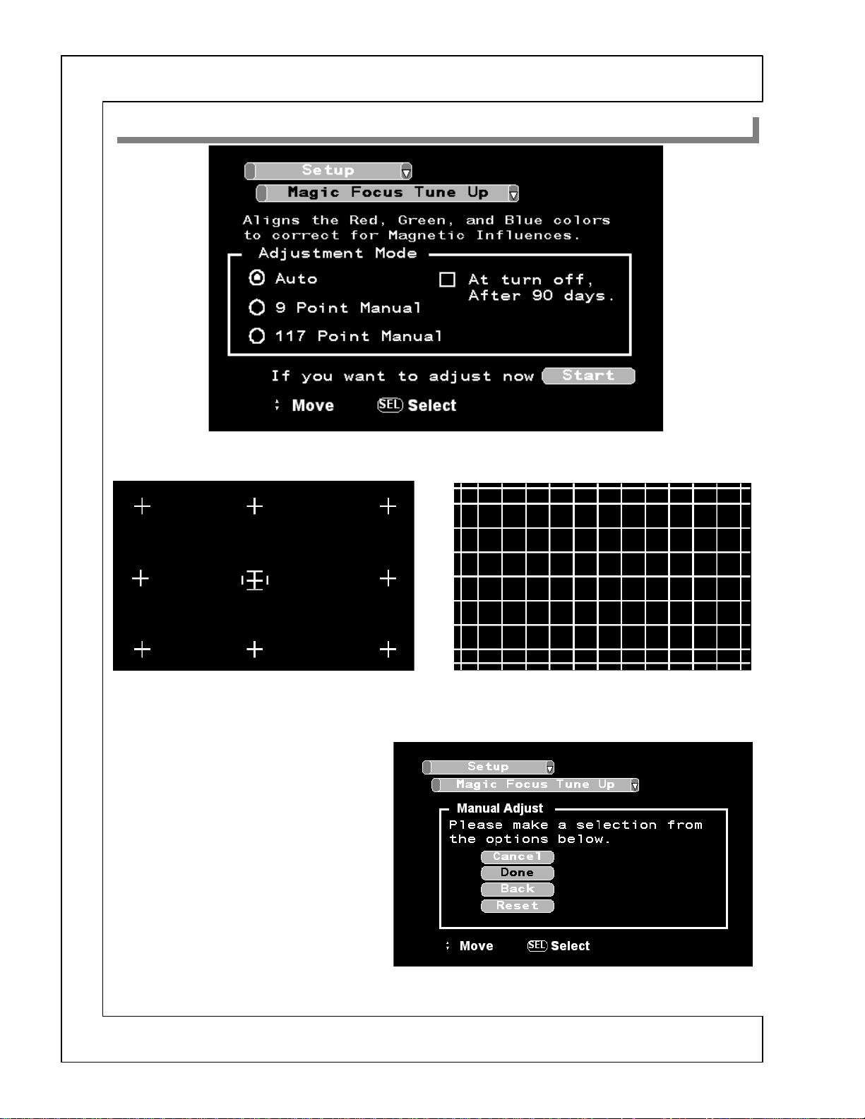
DP-4X DIGITAL CONVERGENCE INTERFACE CIRCUIT EXPLANATION
ever, any manual adjustment data is lost.
If 9 Point Manual Adjustment was Selected: This
represents the Grid Display.
After making any adjustment in either 9 Point or 117 Point, press the
Then the Manual Adjustment Mode Menu will
appear. See Figure to the Right.
At this point, the customer can make the following selections:
•
Cancel:
made and return the set to the condition it
was in before any adjustments were made.
•
Done:
adjustment data.
•
Back:
justment mode grid, either 9 Point or 117
Point so the customer can continue making
adjustments.
•
Reset:
convergence it was in before making any
adjustments..
This will cancel any adjustments
This will memorize the Customer's
This will return to the the Last Ad-
Puts the set back into the state of
If 117 Point Manual Adjustment was Selected:
This represents the Grid Display.
key.
EXIT
PAGE 06-05
Page 86

DP-4X CHASSIS "DIGITAL CONVERGENCE" INTERCONNECTION CIRCUIT DIAGRAM
Magic Focus
Ft. Control PWB
1
IR Out
HMO1
IR Receiver
3
PAGE 06-06
IR Out
HMO2
IR Receiver
1
17
SM09
QM05
QM01
DM13
IY05
2
3
2 1
PFT1
21
3
2
6
1
5
8
2
PFS
QY17
I009
3.3V
-5V
+3.3V
Q031Q032
BUSY
IR In
Stby
45
MAG SW In (Lo)
55
DCU IR Out
56
DCU IR Sel
614
50
Digicon Adj
713
44
Magic Sw Out
Digicon
42
Busy In
6
MAG SW
Signal PWB
Sensor PWB
LED
S0 ~S7
8 Total
Sensors
IR
I004
Main
+5V
Gnd
OSD B
OSD G
OSD R
Up
PDS1
PDSE
S7
S6
S5
S4
S3
S2
S1
S0
Signal PWB
OSD B
34
OSD G
33
OSD R
32
Dig OSD B
Dig OSD G
Dig OSD R
QY34
QY32
QY22
Service Only
SK01
Sw Adj
6
2
9
1
3
4
8
5
7
DK17
DK16
From QK01
From IK01
DCU YS
Busy
D Adj
Dig R
IR-In
Dig G
Dig B
MAG SW
-5V
+5V
H Blk
D Size
V Blk
10
9
8
7
6
5
4
3
2
1
+5V Digital
From IK01
Deflection PWB
Gnd
S7
S6
S5
S4
S3
S2
S1
S0
15
Sw Adj
31
UKDG
HC2611
25
17
D Adj
23
21
27
19
29
MAG SW
Digital
Convergence
44
40
32
35
36
Unit
"DCU"
"Mounted on
Deflection
PWB"
13
16
18
20
22
24
26
28
30
"DCAM"
Digital Convergence
Adjustment Mode
PDG
QY29
QY24
Rainforest
QY25
QY26
SW+28P
SW-28P 3
BV
13
BH
10
GV
8
14
33
34
38
42
-5V
GH
6
RV
4
RH
2
RK09
Mute
1
RK10
DK15
26
OSD B
25
OSD G
24
OSD R
18
Dig OSD B
Dig OSD G
19
21
Dig OSD R
2 YS3
PPDC
1
PDCU
9
8
7
3
2
6
5
4
1
QK04
3
Mute
"Lo"
IY04
Out PWB
Spot
IK02
2
Mute
DK70
RK75
Conv.
B
14
G
13
R
12
10
5
15 16
2
14
6
SW-28P
5
GH
10
15 16
Mute
1
RK12
IK40
2
RV
14 13
6
RH
RK11
QY56
QY54
QY52
-
+
IK41
-
+
-
+
-
+
-
+
-
+
BV
BH
GV
4817 12
4817 12
18
11
13
9
7
18
CYV+
11
CYH+
9
7
SW+28V
CYV+
CYV-
CYH+
CYH-
CYH+
CYH-
CYV-
CYV+
CYV-
CYH-
PSC
9
B
To CRTs
7
G
5
R
To Blue Convergence Yokes
PCB
1
3
6
4
PCG
6
To Green Convergence
4
Yokes
3
1
To Red Convergence Yokes
PCR
1
3
4
6
Page 87

DP-47 REMOTE CONTROL CLU-3842WL HL02062
When Convergence is adjusted
by this Remote,
this Remote must be changed to
DCU mode.
Remote begins in TV mode.
While holding the "ENT" key,
press "MENU" then "INFO" keys.
TV LED will blink 3 times.
Can not change Source Access.
INITIALIZE
(Aspect then Stop) Keys
Pressed by itself produces
extra lines at outside edge.
TV DVD CBL STB PVR AMP
SOURCE ACCESS
ENT
ASPECT
DAY/NIGHT
PIP
To return to normal TV mode.
Remote begins in TV mode.
Hold down the ENT key and
enter 1345 (Hitachi Pre-Code).
RASTER POSITION
Volume Up and Down is a Wheel.
Pressing acts as a button for MUTE.
Channel Up and Down is a Wheel.
Pressing acts as a button for
FAV CH (Favorite Channel).
ROM WRITE Press twice.
CALCULATE
REMOVE COLOR
Outside Signal + Grid
Outside Signal + Cursor
Outside Signal w/o Cursor
ADJUSTMENT
DCU PHASE in DCAM
then press EXIT
MUTE Clears Warning Displays
NOTE: Sensor Error Code place
Remote and TV in DCAM,
press DAY/NIGHT then
ADJUSTMENT POINT UP
ADJUSTMENT POINT DOWN
ADJUSTMENT POINT LEFT
GUIDE
SELECT
C.C. INFO
INPUTS
VOL
(PUSH TO
MUTE)
(PUSH FOR
FAV CH)
1 2 3
4 5 6
EXITMENU
CH
SINGLE CROSSHAIR
ROM READ Press twice.
(Read Old ROM Data)
CROSSHATCH / VIDEO
(Press 5 Times)
Toggles between Red and
Blue Adjustment Mode
GREEN Select
3X3 Mode (Press 5 Times)
BLUE Select
13X9 Mode
(Press 5 Times)
CH UP Moves
Adjustment Point
Counter Clockwise
Spiraling Outward
CH DW Moves
Adjustment Point
Clockwise Spiraling
Outward
NOTE: The 3X3 mode can only
be entered after the RAM is
cleared.
With Power Off press and hold
the Service Only switch.
Then Press the Power Button.
7 8 9
0
HITACHI
HITACHI
HITACHIHITACHI
LC
ADJUSTMENT
POINT RIGHT
Removes
Adjustment Marker
RED Select
7X5 Mode
(Press 5 Times)
PAGE 06-07
Page 88

DP-43 and DP-45 REMOTE CONTROL CLU-4341UG2
When Convergence is
adjusted by this Remote,
this Remote must be changed
to DCU mode.
Remote begins in TV mode.
Press and hold the "TV" key.
Press all at one time, "MENU,
INFO and (-) DASH" keys.
(p/n HL02071)
POWER
VCR
INPUTS ASPECT PIP
CBLDVD
TV
SAT
DAY/NIGHT
To return to normal TV mode.
Press and hold the "TV" key.
Press the "0" then "1" keys.
ROM WRITE
ROM READ
(Read Old ROM Data)
BLUE Select
13X9 Mode
(5 Times)
REMOVE COLOR
Outside Signal + Grid
Outside Signal + Cursor
Outside Signal w/o Cursor
NOTE: Sensor Error Code place
in DCAM, place TV in DCAM,
press DAY/NIGHT then
CURSOR UP
CURSOR DOWN
CURSOR LEFT
RED Select
7X5 Mode (5 Times)
MENU
SELECT
VOL
FAV CH
MUTE
1
2 3
4 5 6
7 8 9
EXIT
CH
GUIDE
INFO
SINGLE CROSSHAIR
CROSSHATCH / VIDEO
(5 Times)
ADJUSTMENT
CALCULATION
GREEN Select
3X3 Mode (5 Times)
CH UP Moves
Adjustment Point
Counter Clockwise
Spiraling Outward
CH DW Moves
Adjustment Point
Clockwise Spiraling
Outward
INITIALIZE
RASTER POSITION
NOTE: The 3X3 mode can only
be entered after the RAM is
cleared.
With Power Off press and hold
the Service Only switch.
Then Press the Power Button.
0
REC
HITACHI
LC
CURSOR RIGHT
Removes
Adjustment Marker
DCU PHASE
NOTE: DCU Phase
Press
then the EXIT key
PAGE 06-08
Page 89

DP-4X ADJUSTMENT MARKER ON AND OFF CONTROL
ADJUSTMENT MARKER ON AND OFF:
Remote must be in Digital Convergence Adjustment Mode. See page 08-18.
This function can improve view of adjustment point during Digital Convergence Adjustment Mode (DCAM).
When the Service Only switch on the Def/Convergence PWB is pressed, the Digital Convergence Adjustment
Grid appears.
New for this year is the appearance of the Adjustment Point Marker. This Marker is demonstrated in Figure 1
by to two small solid lines that appear at the adjustment point. (See Figure 1)
Adjustment Point is Intersection of Dotted Lines
Marker is NOT displayed.
Figure 1
Press the
tion the two solid lines at the adjustment point disappears and the grid appears as previous years. The Adjustment Point now is the intersection of the dashed colored blinking lines. (See Figure 2)
LAST CH
key on the Remote control, and the display only Normal Crosshatch appears. In this condi-
Adjustment Point Identified by Marker
Adjustment Point Marker.
Figure 2
By repeatedly pressing the
Marker and Non-Display Marker grid.
LAST CH
key on the remote control, the display will toggle between Display
PAGE 06-09
Page 90

DP-4X ADJUSTMENT MARKER MOVEMENT USING CH DW KEY
ADJUSTMENT MARKER MOVES CLOCKWISE SPIRALING OUT BY CH DW KEY:
Remote must be in Digital Convergence Adjustment Mode. See page 08-18.
As always, the adjustment procedure should begin in the Center of the screen and work outward in a Clockwise spiral to the outside of the screen This give the best over all adjustment. New for this year is the activity of
the adjustment point when the CH DW or CH UP key is pressed. The Adjustment point always begins in the
Center position. (See Figure 1)
Adjustment Point Starts in Center
Adjustment Point Marker.
Figure 1
With each press of the
one position Clockwise from the Center. (See Figure 2). Here the Adjustment point (Cursor) has moved on
Stopping Position Clockwise from Center.
CH DW
(Channel Down) key on the Remote control, the adjustment point will move
CH DW
Press
(Channel Down) Marker Moves
Adjustment Point Marker Moves
Clockwise Spiraling Outward.
Figure 2
Continued on Next Page
PAGE 06-10
Page 91

DP-4X ADJUSTMENT MARKER MOVEMENT USING CH DW KEY
ADJUSTMENT MARKER MOVES CLOCKWISE SPIRALING OUT BY CH DW KEY:
(Continued from Previous Page)
As can be seen in the Figure below, (See Figure 3) this identifies the first 25 stopping positions where the adjustment Point will stop with each press of the
117 stopping positions have been accessed.
CH DW
Press
CH DW
(Channel Down) Marker Moves
18 19 20 21 22
17
key on the Remote Control. T his will continue until all
567
23
16
15
4
8
24
123
25
9
1011121314
Adjustment Point Marker Moves
Clockwise Spiraling Outward.
Figure 3
ADJUSTMENT MARKER MOVES COUNTER CLOCKWISE SPIRALING OUT BY CH UP KEY:
With each press of the
Counter Clockwise Spiral fashion to the outside of the screen. Or from the Outside of the screen back to the
Center.
NOTE 1:
There are the following Stopping Point Modes:
117 (13X9) Mode
35 (7X5) Move
9 (3X3) Mode
NOTE 2:
The Adjustment Point is still moved in the Conventio nal way by pressing the following keys;
Move Up = (2) Key, Move Down = (5) Key, Move Right = (6) Key, Move Left = (4) Key
NOTE 3:
Selecting Colors to adjust;
(INFO) selects Green Adjustment Mode, (0) selects Red Adjustment Mode and (IN PUTS) selects Blue.
NOTE 4:
Adjusting the particular location is still accomplished by using the Remotes Cursor Keys, up, down, left and
right.
Entered by pressing Red Select (0) Key pressed 5 times.
(Only be entered with Cleared RAM) Entered by pressing Green Select (
CH UP
(Default) or Entered by pressing Blue Select (
(Channel Up) key on the Remote Control, the adjustment point move s in a
INPUTS
) Key 5 times.
) Key 5 times.
INFO
PAGE 06-11
Page 92

CONVERGENCE USING OUTSIDE SIGNAL SOURCE
Remote must be in Digital Convergence Adjustment Mode. See page 08-18.
By superimposing the digital cross hatch on the main picture or the adjustment point on the main picture, adjustments can be made that are more specific to errors seen while observing the main picture instead of only the
cross hatch pattern.
Press the "Service Only" switch on the Deflection PWB to
bring up the normal Conver gence Cross Hatch pattern.
(Figure 1).
Press the "Menu" button on the remote control. Only display
color selected for adjustment. (Note Green always appears),
in this case, Red is selected, so Red and Green (yellow) lines
appears. (Figure 2).
Marker (Adjustment Point)
Marker
Press the "Menu" button again and the Crosshatch appears
on the main picture. (Figure 3).
Press the "Menu" button again, Marker plus Box marker appears on the main picture. (Figure 4).
Press the "Menu" button again, only Box marker appears on
the main picture. (Figure 5).
Marker
Marker
Only Box Marker
By pressing the "Menu" button, this cycle will repeat.
PAGE 06-12
Page 93

MAGIC FOCUS ERROR CODES FOR THE DP-4X CHASSIS
CONVERGENCE ERRORS:
Remote Must be in DCAM
. See page 08-18.
If an error message or code appears while performing MAGIC FOCUS or initialize (
Digital Convergence Adjustment Mode, follow this confirmation and repair method.
1) Turn on Power and receive any signal.
2) Press the Service Only Switch on the Deflection / Convergence Output PWB.
3) Press
DAY/NIGHT
4) Then press the
button on the Remote Control.
button on the remote control.
STOP
5) Error code will be displayed in bottom right corner of screen.
♦ If there is no error
ERROR!!
Green Dots
Error Code
X
will appear on screen.
CONNECT 1!
No. 1 3
6) Follow repair table for errors.
ERROR!!.
Error
Code
1 VF Error Replace DCU
2
*2
3*2 A/D Lev el Same as Error Code 2
4 Over Flow 1. Check the placement
5 Convergence Same as Error Code 4
Error
Display
Code
Connect 1 1. Darken Outside Light
2. Placing of Sensor
3. Is pattern hitting sensor?
4. Check connection and solder bridge of sensor
5. Replace Sensor.
6. Replace Sensor PWB.
7. Sensor Connector check.
8. Replace DCU.
9. Adjustment check (H/V size, cen tering, R & B
Offset, DCU Character and Sensor Position).
2. Adjustment check (H/V size, cen tering, R & B
Offset, DCU Character and Sensor Position).
3. Conv. Amp. Gain check*1 (check resistor values
only)
Countermeasure
Application
Initialize Magic
Focus
X X
X
—
X X
X
X
X X
ASPECT)
then
Error Message
Sensor Position
SENSOR POSITION
7 3
6
in
1 0
5 4
2
7 Operation Same as Error Code 4
9 Connect 2 Same as Error Code 2
10 Noise Input strong field. Strong signal. Check the wiring of
connector b etween sensor and DCU
11 Sync Input strong field. Strong signal. Check the wiring of
connector b etween sensor and DCU
*1 = RK 53, 54, 57, 58, 61, 62, 65 , 66 , 69, 70, 73 and 7 4 che ck these resistors. *2 = Senso r
— X
X X
X X
X X
PAGE 06-13
Page 94

DP-4X BLANK PAGE “NOTES”
BLANK PAGE
Page 95

CHASSIS
PICTURES
DP-4X
CHASSIS INFORMATION
SECTION 07
Page 96

DP-4X BLANK PAGE “NOTES”
BLANK PAGE
Page 97

DP-4X CHASSIS PICTURES
(08) DP-4X Main Chassis Picture
This picture shows the
tion of a Convergence Output PWB, Tuner PWB, Sub Deflection PWB and HDMI Module.
DP-4X Main Chassis
. The main difference from previous chassis is the addi-
Digital Module
Convergence
Output PWB
DCU
This picture shows a closer view of the
sis is the addition of a Tuner PWB and HDMI Module. Note too that the Antenna Switch controls the
RF to the Main and Sub Tuners as well as the RF to the ATSC Tuner in the Digital Module.
Sub Power
Supply PWB
Sub Power
Supply PWB
Sub Deflection PWB
DP-4X Signal PWB
Digital Module
HDMI
HDMI
. The main difference from previous chas-
Antenna
Switch
Antenna
Switch
Audio Output PWB
Tuner PWB
Flex
Tuner PWB
Flex
Audio Output PWB
PAGE 07-01
Page 98

DP-4X CHASSIS PICTURES
(08) DP-4X Main Chassis Picture Continued.
This picture shows a closer view of the
chassis is the addition of a Convergence Output PWB and the Sub Deflection Module. The Sub Deflection Module contains the Vertical Drive generation IC and the Side Pin Op Amps.
Convergence
Output PWB
DCU
DP-4X Deflection PWB
. The main difference from previous
Sub
Deflection
PWB
This picture shows a close up view of the
DP-4X Convergence Output PWB
using STK-394-250 ICs.
PAGE 07-02
Page 99

DP-4X CHASSIS PICTURES
(08) DP-4X Main Chassis Picture Continued.
This picture shows a close up view of the
Digital
Convergence
Unit
(DCU)
DP-4X Digital Convergence Unit (DCU)
. p/n CS00831A.
This picture shows a close up view of the
directly into the Signal PWB and supplies the low voltage power supplies needed for the chassis. It
also supplies AC to the Deflection Power Supply on the Deflection PWB.
DP-4X Sub (Signal) Power Supply.
(Signal Power)
This PWB is plugged
Sub Power
PWB
PAGE 07-03
Page 100

DP-4X CHASSIS PICTURES
(08) DP-4X Main Chassis Picture Continued.
This picture shows a close up view of the
NTSC Tuners.
DP-4X Tuner PWB
. This PWB contains the Main and Sub
Tuner PWB
Main and
Sub NTSC
Tuners
HDMI COMPARED TO DVI:
This picture shows a close up view of and
tween the two is that HDMI includes Audio. Rem em ber that DVI (without Au di o) is com patib le with
HDMI and HDMI can adapt to DVI with the correct adaptors.
Of course, HDMI to DVI will have no Audio.
The DP-47 will have two HDMI input.
HDMI to DVI adapter cable
. The primary difference be-
DVI HDMI
PAGE 07-04
 Loading...