

Page 1

SERVICE MANUAL
NN TT SS CC
PA
No. 0193
46F510 DP33KA
46F500A DP33KB
DDPP3333KKAA//BB
R/C: CLU-4328UG
CChhaassssiiss
TO GO TO A CHAPTER, CLICK ON ITS HEADING BELOW
CONTENTS
IMPORTANT SAFETY INSTRUCTIONS . . . . . . . . . . . . . . . . . . . . . . . . . . . . . . . . . . . . . 2
SERVICING PRECAUTIONS . . . . . . . . . . . . . . . . . . . . . . . . . . . . . . . . . . . . . . . . . . . . . . 6
TECHNICAL CAUTIONS . . . . . . . . . . . . . . . . . . . . . . . . . . . . . . . . . . . . . . . . . . . . . . . . 11
SPECIFICATIONS . . . . . . . . . . . . . . . . . . . . . . . . . . . . . . . . . . . . . . . . . . . . . . . . . . . . . 12
CAUTIONS WHEN CONNECTING/DISCONNECTING THE HV CONNECTOR . . . . . .13
GENERAL INFORMATION . . . . . . . . . . . . . . . . . . . . . . . . . . . . . . . . . . . . . . . . . . . . . . .14
REMOTE CONTROL . . . . . . . . . . . . . . . . . . . . . . . . . . . . . . . . . . . . . . . . . . . . . . . . . . . .17
CUSTOMIZED PICTURE AND SOUND ADJUSTMENTS . . . . . . . . . . . . . . . . . . . . . . .18
REAR PANEL CONNECTION . . . . . . . . . . . . . . . . . . . . . . . . . . . . . . . . . . . . . . . . . . . . .23
DISPLAY PICTURE FORMATS . . . . . . . . . . . . . . . . . . . . . . . . . . . . . . . . . . . . . . . . . . . .24
SERVICE ADJUSTMENTS . . . . . . . . . . . . . . . . . . . . . . . . . . . . . . . . . . . . . . . . . . . . . . .25
TROUBLESHOOTING FLOW CHART . . . . . . . . . . . . . . . . . . . . . . . . . . . . . . . . . . . . . .69
WAVEFORMS . . . . . . . . . . . . . . . . . . . . . . . . . . . . . . . . . . . . . . . . . . . . . . . . . . . . . . . . .73
DC VOLTAGE TABLES . . . . . . . . . . . . . . . . . . . . . . . . . . . . . . . . . . . . . . . . . . . . . . . . . . .84
PROTECTION CIRCUIT BLOCK DIAGRAM . . . . . . . . . . . . . . . . . . . . . . . . . . . . . . . . . .98
CIRCUIT SCHEMATIC DIAGRAM . . . . . . . . . . . . . . . . . . . . . . . . . . . . . . . . . . . . . . . . . .99
PRINTED CIRCUIT BOARDS . . . . . . . . . . . . . . . . . . . . . . . . . . . . . . . . . . . . . . . . . . . .111
BLOCK DIAGRAM . . . . . . . . . . . . . . . . . . . . . . . . . . . . . . . . . . . . . . . . . . . . . . . . . . . . .124
WIRING DIAGRAM . . . . . . . . . . . . . . . . . . . . . . . . . . . . . . . . . . . . . . . . . . . . . . . . . . . .125
FINAL WIRING DRAWING . . . . . . . . . . . . . . . . . . . . . . . . . . . . . . . . . . . . . . . . . . . . . .126
EXPLODED VIEW . . . . . . . . . . . . . . . . . . . . . . . . . . . . . . . . . . . . . . . . . . . . . . . . . . . . .129
EXPLODED VIEW PARTS LIST . . . . . . . . . . . . . . . . . . . . . . . . . . . . . . . . . . . . . . . . . .131
REPLACEMENT PARTS LIST . . . . . . . . . . . . . . . . . . . . . . . . . . . . . . . . . . . . . . . . . . . .132
DISASSEMBLY INSTRUCTIONS . . . . . . . . . . . . . . . . . . . . . . . . . . . . . . . . . . . . . . . . .155
QUICK REFERENCE PARTS LIST (IC & UNIT) . . . . . . . . . . . . . . . . . . . . . . . . . . . . . .160
CAUTION: These servicing instructions are for use by qualified service personnel only. To reduce the risk of
electric shock do not perform any servicing other than that contained in the operating instructions
unless you are qualified to do so. Before servicing this chassis, it is important that the service
technician read the “IMPORTANT SAFETY INSTRUCTIONS” in this service manual.
SAFETY NOTICE
USE ISOLATION TRANSFORMER WHEN SERVICING
Components having special safety characteristics are identified by a on the schematics and on the parts list in this
Service Data and its supplements and bulletins. Before servicing the chassis, it is important that the service technician
read and follow the “Important Safety Instructions” in this Service Manual.
!
SPECIFICATIONS AND PARTS ARE SUBJECT TO CHANGE FOR IMPROVEMENT
PROJECTION COLOR TELEVISION
AUGUST 2004 HHEA-MANUFACTURING DIVISION
Page 2

IMPORTANT SAFETY INSTRUCTIONS
USE ISOLATION TRANSFORMER WHEN SERVICING
DP33KA/B
Components having special safety characteristics are identified by a on the schematics and on the parts list in this service
ual and its supplements and bulletins. Before servicing this chassis, it is important that the service technician read and
man
follow the “Important Safety Instructions” in this Service Manual.
For continued X-Radiation protection, replace picture tube with original type or Hitachi approved equivalent type.
This Service Manual is intended for qualified service technicians; it is not meant for the casual do-it-yourselfer. Qualified
technicians have the necessary test equipment and tools, and have been trained to properly and safely repair complex
products such as those covered by this manual.
Improperly performed repairs can adversely affect the safety and reliability of the product and may void warranty. If you
are not qualified to perform the repair of this product properly and safely, you should not risk trying to do so and refer the
repair to a qualified service technician.
!
WARNING
Lead in solder used in this product is listed by the California Health and Welfare agency as a known reproductive toxicant which
may cause birth defects or other reproductive harm (California Health and Safety Code, Section 25249.5).
When servicing or handling circuit boards and other components which contain lead in solder, avoid unprotected skin contact
with solder. Also, when soldering do not inhale any smoke or fumes produced.
This television receiver provides display of television closed captioning in accordance with section 15.119 of the FCC rules.
FEDERAL COMMUNICATIONS COMMISSION NOTICE
This equipment has been tested and found to comply with the limits for a Class B digital device, pursuant to Part 15 of the
FCC Rules. These limits are designed to provide reasonable protection against harmful interference in a residential
installation. This equipment generates, uses, and can radiate radio frequency energy and, if not installed and used in
accordance with the instructions, may cause harmful interference to radio communications. However, there is no guarantee
that interference will not occur in a particular installation. If this equipment does cause harmful interference to radio or
television reception, which can be determined by turning the equipment off and on, the user is encouraged to try to correct
the interference by one or more of the following measures:
ient or relocate the receiving antenna.
• Reor
• Increase the separation between the equipment and the receiver.
• Connect the equipment into an outlet on a circuit different from that to which the receiver is connected.
• Consult the dealer or an e
xperienced radio/television technician for help.
TABLE OF CONTENTS
2
Page 3
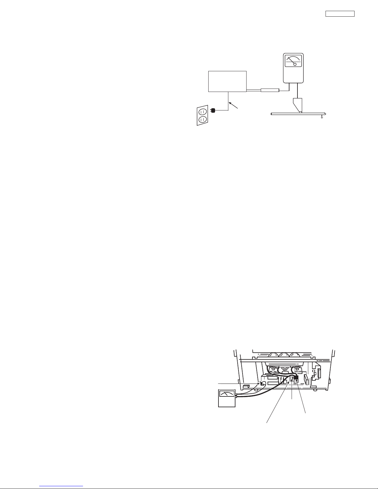
IMPORTANT SAFETY INSTRUCTION
Chassis
ground
High Impedance
H.V. meter
Deflection P.W.B.
FBT
(TH01)
High voltage
connector
+
-
LEAKAGE
CURRENT
TESTER
DEVICE
UNDER
TEST
TEST ALL
EXPOSED
METAL
SURFACES
2-WIRE CORD
(READING
SHOULD NOT
BE ABOVE
0.5 mA)
EARTH
GROUND
ALSO TEST WITH
PLUG REVERSED (USING
AC ADAPTER PLUS
AS REQUIRED)
Before returning an instrument to the customer, always
1.
make a safety check of the entire instrument, including
but not limited to the following items.
Be sure that no built-in protective devices are
a.
defective and/or have been deleted during servicing.
(1) Protective shields are provided on this chassis to
protect both the technician and the customer
Correctly replace all missing protective shields,
including any removed for servicing convenience. (2)
When reinstalling the chassis and/or other assemb
in the cabinet, be sure to put back in place all
protective devices, including but not limited to,
nonmetallic control knobs
adjustment and compartment covers/shields, and
isolation resistor/capacitor networks.
this instrument or permit it to be operated without
all protective devices correctly installed and
functioning.
Servicers who defeat safety features
or fail to perform safety checks may be liable for
any resulting damage.
b. Be sure that there are no cabinet openings through
which an adult or child might be able to insert their
fingers and contact a hazardous voltage. Such
openings include, but are not limited to (1) spacing
between the picture tube and cabinet mask, (2)
excessively wide cabinet ventilation slots, and (3) an
improperly fitted and/or incorrectly secured cabinet
back cover.
Antenna Cold Check – With the instrument AC plug
c.
removed from any AC source, connect an electrical
jumper across the two AC plug prongs. Place the
instrument AC switch in the on position. Connect one
lead of an ohmmeter to the AC plug prongs tied
together and touch the other ohmmeter lead in turn to
each tuner antenna input, exposed terminal screw
and, if applicable, to the coaxial connector. If the
measured resistance is less than 1.0 megohms or
greater than 5.2 megohms, an abnormality exists that
must be corrected before the instrument is returned to
Repeat this test with the instr
the customer
witch in the off position.
s
.
, insulating fishpaper,
Do not operate
ument A
DP33KA/B
(READING
SHOULD NOT
BE ABOVE
0.5 MIU)
.
ly
AC Leakage Test
AC LEAKAGE TEST
ANY MEASUREMENTS NOT WITHIN THE LIMITS
OUTLINED ABOVE ARE INDICATIVE OF A POTENTIAL
SHOCK HAZARD AND MUST BE CORRECTED BEFORE
RETURNING THE RECEIVER TO THE CUSTOMER.
e. High Voltage – This receiver is provided with a
hold down circuit for clearly indicating that voltage has
increased in excess of a predetermined value.
Comply will all notes described in this Service Manual
regarding this hold down circuit when servicing, so
that this hold down circuit may correctly be operated.
Service Warning – With maximum contrast, operating
f.
high voltage in this receiver is lower than
30.5 kV. In
case any component having influence on high voltage
is replaced, confirm that the high voltage with
maximum contrast is lower than
30.5 kV.
To measure H.V. use a high impedance H.V. meter.
Connect (-) to chassis earth and (+) to the CRT anode
utton. (See the following connection diagram.)
b
C
Note: Turn power switch off without fail before the
connection to the anode button is made.
Leakage Current Hot Check -
d.
directly into a 120V
AC 60Hz outlet
isolated transformer for this check). Turn the A C
ON. Using a Leakage Current
power
Model 228 or equivalent), measure for current from all
exposed metal parts of the cabinet (antennas,
screwheads,
overlays, control shafts, etc.)
particularly any exposed
having a return path to the chassis or to a
known earth ground (water pipe, conduit, etc.).
current measured must not exceed 0.5 MIU.
Plug the
(do not use an
ester (Simpson’
T
metal
AC line cord
s
part
Any
3
Page 4
Shield Plate A
Glass Lens for Shielding
Shield Plate B
Shield Plate C
Shield Plate D
Detailing X-radiation shield
Shield Plate C
IMPORTANT SAFETY INSTRUCTIONS
DP33KA/B
g. X-radiation – TUBE: The primary source of X-
radiation in this receiver is the picture tube. The tube
utilized for the above mentioned function in this
chassis is specially constructed to limit X-radiation
emissions.
For continued X-radiation protection, the replacement
tube must be the same type as the original, Hitachi
approved type.
When troubleshooting and making test measurements in a receiver with a problem of excessive high
voltage, avoid being unnecessarily close to the picture
tube and the high voltage component.
Do not operate the chassis longer than is necessary
to locate the cause of excessive voltage.
X-radiation Shield –
h.
1. This receiver is provided with X-ray shield plates
for protection against X-radiation. Do not remove
X-ray shield plates A, B, or C shown in Fig. 1
unnecessarily, when troubleshooting and/or
making test measurements.
2. To prevent X-radiation, after replacement of
picture tube and lens, confirm these components
to be fixed correctly to bracket and cabinet, and
not to be taken off easily.
Installation of shield lens,
1.
Fig.
shield cover and shield plates (oblique view).
4
Page 5

IMPORTANT SAFETY INSTRUCTIONS
DP33KA/B
Read and comply with all caution and safety-related
2.
notes on or inside the receiver cabinet, on the receiver
chassis, or on the picture tube.
3.
Design Alteration Warning – Do not alter or add to
the mechanical or electr
Design alterations and additions including but not
limited to circuit modifications and the addition of
items such as auxiliar
connectors, might alter the safety characteristics of
this receiver and create a hazard to the user. Any
design alter
manufacturer’s warranty and may make you, the
servicer, responsible for personal injury or property
damage resulting therefrom.
Picture Tube Implosion Protection Warning – The
4.
picture tube in this receiver employs integral implosion
protection. For continued implosion protection,
replace the picture tube only with one of the same
type number. Do not remove, install, or otherwise
handle the picture tube in any manner without first
putting on shatterproof goggles equipped with side
shields. People not so equipped must be kept safely
away while picture tubes are handled. Keep the
picture tube away from your body. Do not handle the
picture tube by its neck.
ations or additions may void the
ical design of this TV receiver.
y audio and/or video output
7. Components, parts, and/or wiring that appear to have
verheated or are otherwise damaged should be
o
replaced with components, parts, or wiring that meet
original specifications. Additionally, determine the
cause of o
necessary, take corrective action to remove any
potential safety hazard.
PRODUCT SAFETY NOTICE – Many TV electrical
8.
and mechanical parts have special safety-related
characteristics some of which are often not evident
from visual inspection, nor can the protection the
e necessarily be obtained by replacing them with
giv
components rated for higher voltage, wattage, etc.
Parts that have special safety characteristics are
identified in Hitachi service data by shading on
schematics and by a in the parts list. Use of
substitute replacement that does not have the same
safety characteristics as the recommended replacement part in Hitachi service data parts list might
create shock, fire, and/or other hazards. Product
safety is under review continuously and new
instructions are issued whenever appropriate. For the
latest information, always consult the appropriate
current Hitachi service literature. A subscription to, or
additional copies of service literature may be obtained
at a nominal charge from Hitachi.
verheating and/or damage and, if
!
y
Hot Chassis Warning – a. Some TV receiver chassis
5.
are electrically connected directly to one conductor of
the AC power cord and may be safely serviced without
an isolation transformer only if the AC power plug is
inserted so that the chassis is connected to the
ground side of the AC power source. Confirm that the
AC power plug is inserted correctly with an AC
voltmeter by measuring between the chassis and a
known earth ground. If a voltage reading in excess of
1.0V is obtained, remov
plug in the opposite polarity and again measure the
voltage potential between the chassis and a known
earth ground.
have 85V AC (RMS) between chassis and earth
ground regardless of the AC plug polarity. These
chassis can be safely serviced only with an isolation
transformer inserted in the power line between the
receiver and the AC power source, for both personnel
and test equipment protection.
chassis have a secondary ground system in addition
to the main chassis ground. This secondary ground
system is not isolated from the AC power line.The two
ground systems are electrically separated by
insulating material that must not be defeated or
altered.
6. Observe original lead dress. Take extra care to assure
correct lead dress in the following areas:
edges,
and components do not touch thermally hot parts,
the AC supply, d. high voltage and e. antenna wiring.
Always inspect in all areas for pinched, out-of-plate, or
frayed wiring. Do not change spacing between
components and the printed circuit board. Check AC
power cord for damage.
b. Some TV receiver chassis normally
b. near thermally hot parts – be sure that leads
e and reinsert the AC power
c. Some TV receiver
a. near sharp
c.
5
Page 6

SERVICING PRECAUTIONS
CAUTION: Before servicing instruments covered by this
service data and its supplements and addenda, read and
ollow the “Important Safety Instructions” on page 3 of this
f
publication.
NOTE: If unforeseen circumstances create conflict between
ollowing servicing precautions and any of the safety
the f
precautions on page 3 of this publication, always follow the
safety precautions. Remember: Safety First.
DP33KA/B
7. Do not apply AC power to this instrument and/or any of its
electrical assemblies unless all solid-state device heatsinks are correctly installed.
8. Always connect the test instrument ground lead to the
appropr
the test instrument positive lead. Always remove the test
instrument ground lead last.
iate instrument chassis ground before connecting
General Servicing Guidelines
Always unplug the instrument AC power cord from the AC
1.
power source before:
a. Removing or reinstalling any component, circuit
board, module
b. Disconnecting or reconnecting any instrument
electrical plug or other electrical connection.
c. Connecting a test substitute in parallel with an
electrolytic capacitor in the instrument.
UTION:
CA
d. Discharging the picture tube anode.
2. Test high voltage only by measuring it with an appropriate
high voltage meter or other voltage measuring device
(DVM, FETVOM, etc.) equipped with a suitable high
voltage probe. Do not test high voltage by “drawing an
arc.” The H.V. Distribution Box has an internal 400M
resistor (bleeder resistor) connected from the high
voltage to ground. After power is removed from the
instrument the high voltage will discharge through the
high voltage bleeder resistor. If the tubes have high
voltage after power is removed, then the bleeder resistor
is defective or the bleeder ground is disconnected.
, or any other instrument assembly.
A wrong par
polarity installation of electrolytic
capacitors may result in an explosion
hazard.
t substitution or incorrect
9. Use with this instrument only the test fixtures specified in
this service data.
CAUTION: Do not connect the test fixture ground strap
to any heatsink in this instrument.
Electrostatically Sensitive (ES) Devices
Some semiconductor (solid state) devices can be damaged
easily by static electricity. Such components commonly are
called Electrostatically Sensitive (ES) Devices. Examples of
typical ES devices are integrated circuits and some fieldeffect transistors and semiconductor “chip” components. The
following techniques should be used to help reduce the
incidence of component damage caused by static electricity.
1. Immediately before handling any semiconductor
component or semiconductor-equipped assembly, drain
off any electrostatic charge on your body by touching a
known earth ground. Alternatively, obtain and wear a
commercially available discharging wrist strap device,
which should be removed for potential shock reasons
prior to applying power to the unit under test.
Ω
2. After removing an electrical assembly equipped with ES
devices, place the assembly on a conductive surface
such as aluminum foil, to prevent electrostatic charge
buildup or exposure of the assembly.
3. Use only a grounded-tip soldering iron to solder or
desolder ES devices.
3. Discharge the picture tube’s anode at any of the R, G, or
B outputs on the H.V. Distribution Box only by (a) first
connecting one end of an insulated clip lead to the
degaussing or kine aquadag g
the point where the picture tube socket ground lead is
connected, and then (b) touch the other end of the
insulated clip lead to the picture tube high voltage
distribution box R, G, or B output, using an insulated
oid personal contact with high voltage.
handle to a
4. Do not spray chemicals on or near this instrument or any
of its assemb
5. Unless specified otherwise in these service data, clean
electr
the contacts with a pipe cleaner, cotton-tipped stick or
comparable nonabrasive applicator: 10% (by volume)
Acetone and 90% (b
99% strength).
CAUTION: This is a flammable mixture. Unless
6. Do not defeat any plug/socket B+ voltage interlocks with
which instruments covered by this service data might be
equipped.
v
.
lies
ical contracts by applying the following mixture to
y volume) isopropyl alcohol (90%-
specified otherwise in these ser
lubrication of contacts is not required.
rounding system shield at
TABLE OF CONTENTS
vice data,
4. Use only can anti-static type solder removal device.Some
solder removal devices not classified as “anti-static” can
generate electrical charges sufficient to damage ES
device.
5. Do not use freon-propelled chemicals. These can
generate electrical charges sufficient to damage ES
devices.
6. Do not remove a replacement ES device from its
protective package until immediately before you are ready
to install it. (Most replacement ES devices are packaged
with leads electrically shorted together by conductive
foam, aluminum foil or comparable conductive material.)
7. Immediately before removing the protective material from
the leads of a replacement ES device, touch the
protective material to the chassis or circuit assembly into
which the device will be installed.
CAUTION: Be sure no power is applied to the chassis or
circuit, and observe all other safety
precautions
8. Minimize bodily motions when handling unpackaged
replacement ES de
such as the brushing together of your clothes fabric or the
lifting of your foot from a carpeted floor can generate
6
static electr
icity sufficient to damage an ES device.)
.
. (Otherwise harmless motion
vices
Page 7
Use Solding Iron to Pry Leads
SERVICING PRECAUTIONS
General Soldering Guidelines
1. Use a grounded-tip, low-wattage soldering iron and
appropr
temperature within the range 500°F to 600°F.
Use an appropriate lead free solder (see page 10). Lead
2.
solder can be used, but there is a possibility of failure due
to insufficient strength of the solder.
iate tip size and shape that will maintain tip
DP33KA/B
Removal
1. Desolder and straighten each IC lead in one operation by
gently prying up on the lead with the soldering iron tip as
the solder melts.
2. Draw away the melted solder with an anti-static suctiontype solder removal device (or with solder braid) before
removing the IC.
3. Keep the soldering iron tip clean and well-tinned.
Thoroughly clean the surfaces to be soldered. Use a
4.
small wire-bristle (0.5 inch or 1.25 cm) brush with a metal
handle. Do not use freon-propelled spray-on cleaners.
5. Use the following desoldering technique.
a. Allow the soldering iron tip to reach normal
temperature (500°F to 600°F).
b. Heat the component lead until the solder melts. Quickly
draw away the melted solder with an anti-static,
suction-type solder removal device or with solder
braid.
CAUTION: Work quickly to avoid overheating the
circuit board printed foil.
6. Use the following soldering technique.
a. Allow the soldering iron tip to reach normal
temperature (500°F to 600°F).
b. First, hold the soldering iron tip and solder strand
against the component lead until the solder melts.
c. Quickly move the soldering iron tip to the junction of
the component lead and the printed circuit foil, and
hold it there only until the solder flows onto and
around both the component lead and the foil.
CAUTION: Work quickly to avoid overheating the
circuit board printed foil or components.
Replacement
1. Carefully insert the replacement IC in the circuit board.
2. Carefully bend each IC lead against the circuit foil pad
and solder it.
3. Clean the soldered areas with a small wire-bristle brush.
(It is not necessary to reapply acrylic coating to areas.)
“Small-signal” Discrete Transistor Removal/Replacement
1. Remove the defective transistor by clipping its leads as
close as possible to the component body.
2. Bend into a “U” shape the end of each of three leads
remaining on the circuit board.
3. Bend into a “U” shape the replacement transistor leads.
4. Connect to replacement transistor leads to the
corresponding leads extending from the circuit board and
crimp the “U” with long nose pliers to insure metal to
metal contact, then solder each connection.
Power Output Transistor Devices Removal/Replacements
1. Heat and remove all solder from around the transistor
leads.
2. Remove the heatsink mounting screw (if so equipped).
3. Carefully remove the transistor from the circuit board.
d. Closely inspect the solder area and remove any excess
or splashed solder with a small wire-bristle brush.
al/Replacement
IC Remo
Some Hitachi unitized chassis circuit boards have slotted
holes (oblong) through which the IC leads are inserted and
then bent flat against the circuit f
slotted type, the following technique should be used to
remove and replace the IC.When working with boards using
the familiar round hole
outlined in paragraphs 5 and 6 above.
v
When holes are the
oil.
, use the standard technique as
4. Insert new transistor in circuit board.
5. Solder each transistor lead, and clip off excess lead.
Replace heatsink.
6.
Diode Removal/Replacement
1. Remove defective diode by clipping its leads as close as
possible to diode body.
2. Bend the two remaining leads perpendicularly to the
circuit board.
3. Observing diode polarity, wrap each lead of the new
diode around the corresponding lead on the circuit board.
4. Securely crimp each connection and solder it.
5. Inspect (on the circuit board copper side) the solder joints
of the two “original leads”. If they are not shiny, reheat
them and, if necessary, apply additional solder.
7
Page 8

CRIMP AND
SOLDER
BARE JUMPER
WIRE
Install Jumper Wire and Solder
DEFECTIVE
COPPER
REMOVED
Insulated Jumper Wire
SERVICING PRECAUTIONS
Fuses and Conventional Resistor Removal/Replacement
1. Clip each fuse or resistor lead at top of circuit board
w stake.
hollo
2. Securely crimp leads of replacement component around
e 1/8 inch from top.
stak
3. Solder the connections.
UTION:
CA
Maintain or
replaced component and adjacent
components and the circuit board, to
vent excessive component
pre
temperatures.
Circuit Board Foil Repair
Excessive heat applied to the copper foil of any printed
circuit board will w
eaken the adhesive that bonds the foil to
the circuit board, causing the foil to separate from, or “lift-off,”
the board. The following guidelines and procedures should
be followed whenever this condition is encountered.
In Critical Copper Pattern Areas
High component/copper pattern density and/or special
voltage/current characteristics make the spacing and
integrity of copper pattern in some circuit board areas more
critical than in others. The circuit foil in these areas is
designated as Critical Copper Pattern. Because Critical
Copper Pattern requires special soldering techniques to
ensure the maintenance of reliability and safety standards,
contact your Hitachi personnel.
iginal spacing between the
DP33KA/B
At Other Connections
Use the following technique to repair defective copper
pattern at connections other than IC Pins. This technique
involves the installation of a jumper wire on the component
side of the circuit board.
1. Remove the defective copper pattern with a sharp knife.
Remove at least 1/4 inch of copper, to ensure hazardous
condition will not exist if the jumper wire opens.
2. Trace along the copper pattern from both wire sides of the
pattern break and locate the nearest component directly
connected to the affected copper pattern.
At IC Connections
To repair defective copper pattern at IC connections, use the
following procedure to install a jumper wire on the copper
pattern side of the circuit board. (Use this technique only on
IC connections.)
1. Carefully remove the damaged copper pattern with a
sharp knife. (Remove only as much copper as absolutely
necessary.)
2. Carefully scratch away the solder resist and acrylic
coating (if used) from the end of the remaining copper
pattern.
gauge jumper wire
in one end of a small
Bend a small
3.
and carefully cr
connection.
4. Route the jumper wire along the path of the cut-away
copper pattern and let it overlap the previously scraped
end of the good copper patter
area, and clip off any excess jumper wire.
“U”
imp it around the IC pin. Solder the IC
-
Solder the o
n.
v
erlapped
3. Connect insulated 20-gauge jumper wire from the
nearest component on one side of the pattern break to
the lead of the nearest component on the other side.
Carefully crimp and solder the connections.
CAUTION: Be sure the insulated jumper wire is
dressed so that it does not touch
components or sharp edges.
Frequency Synthesis (FS) Tuning Systems
1. Always unplug the instrument AC power cord before
disconnecting or reconnecting FS tuning system cables
and before removing or inserting FS tuning system
modules
.
2. The FS tuner must never be disconnected from the FS
tuning control module while power is applied to the
instrument.
3. When troubleshooting intermittent problems that might be
caused by defective cable connection(s) to the FS tuning
system, remove the instrument AC power as soon as the
defective connector is found and finish confirming the bad
connection with a continuity test. This procedure will
reduce the probability of electrical overstress of the FS
system semi-conductor components.
8
Page 9
SERVICING PRECAUTIONS
DP33KA/B
NOTE: These components are affixed with glue. Be careful not to break or damage any foil under the
component or at the pins of the ICs when remo
ving. Usually applying heat to the component for a short
time while twisting with tweezers will break the component loose.
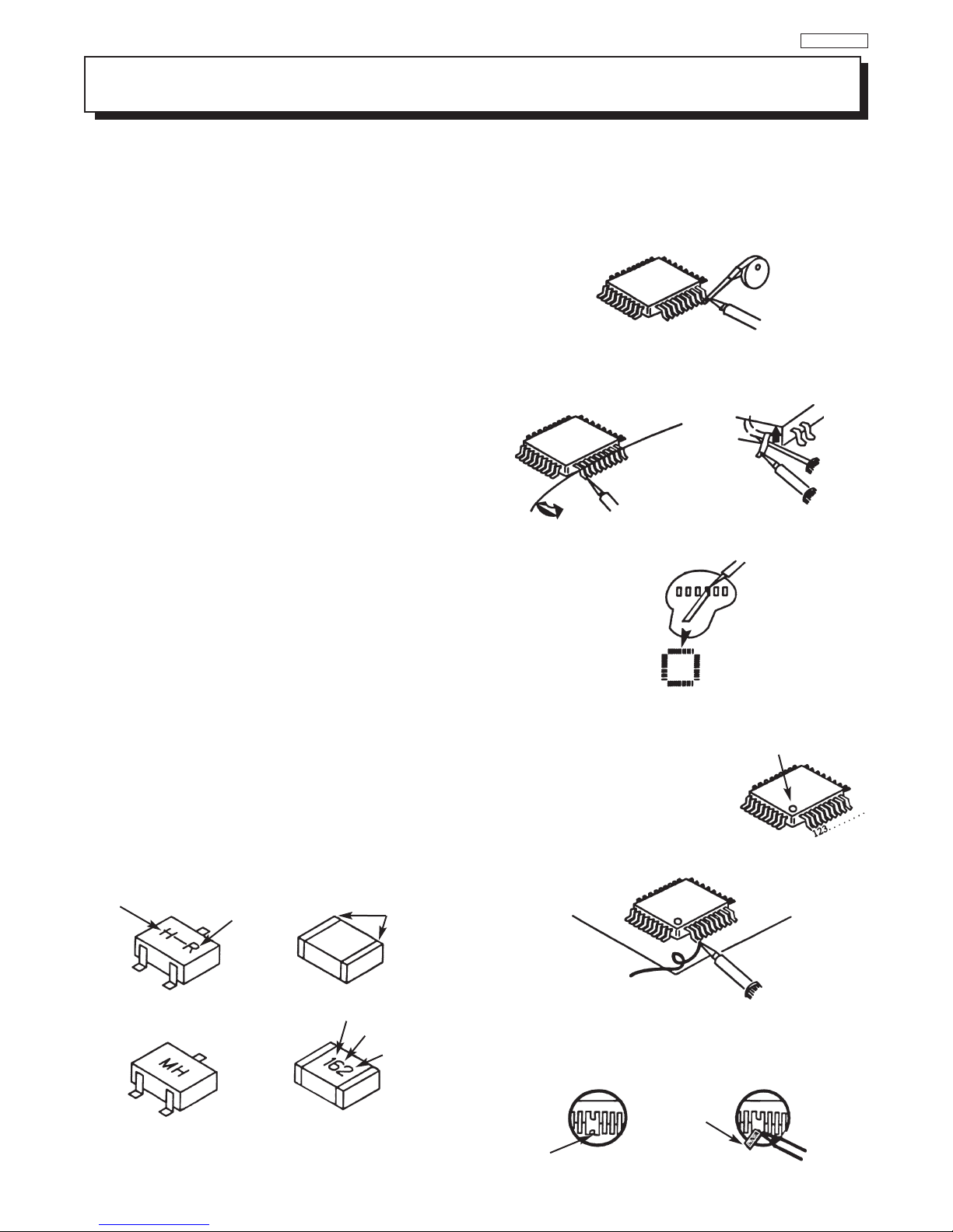
Leadless Chip Components
(surface mount)
Chip components must be replaced with identical
chips due to critical foil track spacing. There are no
holes in the board to mount standard transistors or
diodes. Some chip capacitor or resistor board solder
pads may have holes through the board, however the
hole diameter limits standard resistor replacement to
1/8 watt. Standard capacitors may also be limited for
the same reason. It is recommended that identical
chip components be used. .
Chip resistors have a three digit numerical resistance
code -1st and 2nd significant digits and a multiplier.
Example:
162 = 1600 or 1.6KΩ resistor, 0 = 0Ω
(jumper).
Chip capacitors generally do not have the value
indicated on the capacitor.The color of the component
indicates the general range of the capacitance.
Chip transistors are identified by a two letter code.The
first letter indicates the type and the second letter, the
grade of transistor.
Chip diodes have a two letter identification code as per
the code chart and are a dual diode pack with either
common anode or common cathode. Check the parts
list for correct diode number.
Component Removal
1. Use solder wick to remove solder from component
end caps or terminals.
2. Without pulling up, carefully twist the component
with tweezers to break the adhesive.
3. Do not reuse removed leadless or chip
components since they are subject to stress
fracture during removal .
Chip Component Installation
1. Put a small amount of solder on the board
soldering pads.
2. Hold the chip component against the soldering
pads with tweezers or with a miniature alligator
clip and apply heat to the pad area with a 30 watt
iron until solder flows. Do not apply heat for more
than 3 seconds
TYPE
Chip Components
C
GRADE
SOLDER
CAPS
How to Replace Flat-lC
—Required Tools—
• Soldering iron • iron wire or small awl
De-solder braids • Magnifier
•
1. Remove the solder from all of the pins of a Flat-lC
by using a de-solder braid.
Flat-IC
2. Put the iron wire under the pins of the Flat-lC and
pull it in the direction indicated while heating the
pins using a soldering iron. A small awl can be
used instead of the iron wire.
Iron
Wire
Pull
Soldering
Iron
Soldering
3. Remove the solder from all of the pads of the
Fiat-lC by using
a de-solder braid.
De-Solder
Braid
Flat-IC
4. Position the new Flat-lC in place (apply the pins of
the Flat-lC to the soldering pads where the pins
need to be soldered). Properly
determine the positions of the
ing pads and pins b
solder
y
correctly aligning the polarity
symbol.
5. Solder all pins to the soldering pads using a fine
tipped soldering iron.
Soldering
Iron
Soldering
Iron
Polarity Symbol
De-Solder
Braid
Iron
A
wl
B
E
COMMON CATHODE
ANODES
MH DIODE
TRANSIST
OR
SOLDER CAPS
RESISTOR
CAPACITOR
1ST DIGIT
2ND DIGIT
MUL
= 1600 = 1.6K
TIPLIER
Solder
Soldering
Iron
6. Check with a magnifier for solder bridge between
the pins or for dry joint between pins and soldering
o remove a solder bridge, use a de-solder braid
T
.
pads
wn in the figure below.
as sho
De-Solder
Braid
Bridge
Solder
9
Soldering
Iron
Page 10
Information for service about lead-free solder introduction
Hitachi introduced lead-free solder to conserve the "Earth Environment".
Please refer to the following before servici
ng.
(1) Characteristic of lead-free solder
Melting point of lead free solder is 40-50
o
C higher than solder containing lead.
(2) Solder for service
Following composition is reccomended.
" Sn - 3.0Ag - 0.5Cu " , or " Sn - 0.7 Cu "
Lead solder can be used, but there is a possibility of fai
lure due to insufficient strength of the solder.
Caution when using solder containing lead.
Please remove previous solder as much as possible from the soldering point.
When soldering, please perfectly melt the lead-free solder to mix well with the previous solder.
(3) Soldering iron for lead-free solder.
Melting point of lead-free solder is higher than solder containing lead.
Use of a soldering tool "with temperature control" and "with much thermal capacitance" is reccomended.
(Reccomended temperature control : 320
o
C - 450oC)
Reccomended temperature
PWB with chip parts
320
o
C +/- 30oC
PWB without chip parts
380
o
C +/- 30oC
Chassis, metal, shield etc.
420
o
C +/- 30oC
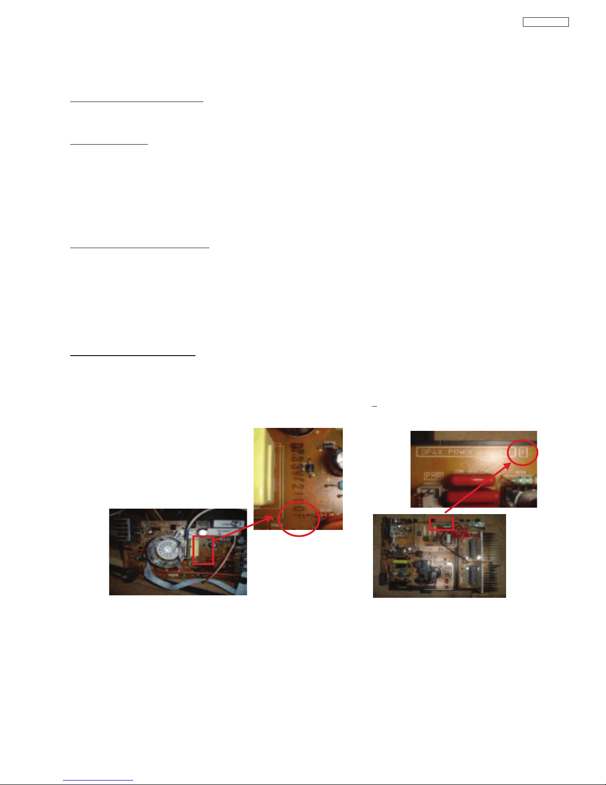
(4) Identification of lead-free PWB
2003 models >> not applied
2003 models >> mixed
2004 models >> lead-free solder is intoduced
On lead-free PWB, "F" is added at the end of stamp on PWB. (e.g. DP33W
F)
DP33KA/B
10
Page 11
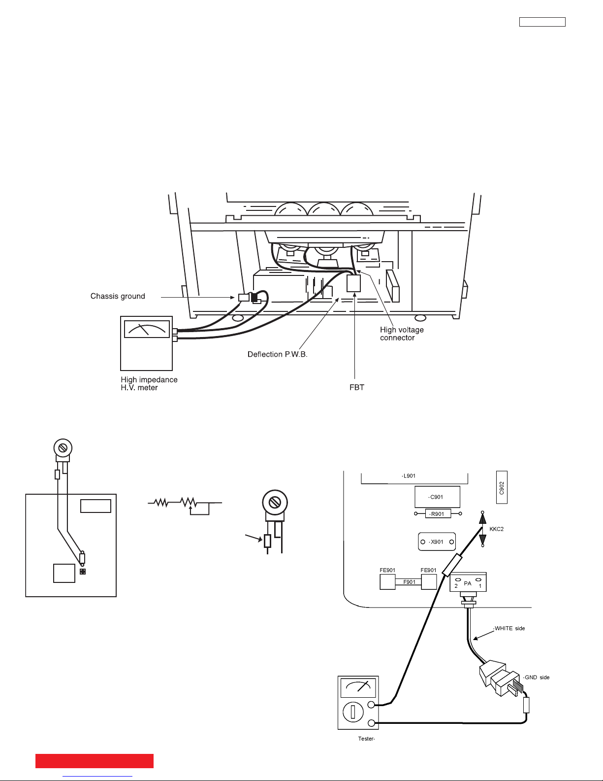
TECHNICAL CAUTIONS
(TH01)
D.C.U
RH19
RH17
Fig. 2. Power/Deflection P.W.B
Remove RH19 and connect 50KΩ VR jig as shown.
TH02
FBT
50KΩ VR
50KΩ VR
33KΩ
Resistor
33KΩ
Voltage limiter circuit operation check.
High
1. Turn off TV and connect jig as shown in Figure 2. Adjust
jig fully counter-clockwise for minimum resistance.
DP33KA/B
4. When the limiter circuit is operating properly, High
Voltage will be less than 31 kV at 1.72mA when TV shuts
wn.
do
2. Set the AC input to 120V AC and turn on TV.
Confirm test pattern on CRT is a usable picture, then
3.
slowly adjust jig until the picture disappears and TV shuts
down.
5. Turn off set immediately after checking circuit operation.
6. Unplug set for one minute to reset shutdown circuit.
Remove jig and voltmeter.
AC CORD POLARITY
This check is based on the UL standard. Use the jigs
specified by the production technology section. The GND
side (wider blade) of the AC power cord should be
connected to K9Y1
TABLE OF CONTENTS
11
Page 12
125V
10A
F
10 A 125V
SPECIFICATIONS
DP33KA/B
Models: 46F510/46F500A
Cathode-Ra
y Tube:
46F510 R=P16LXS00RFA B
46F500A G=P16LXS00HHA B
B=P16LXS00BMB B
Power Input: 120 volts AC, 60 Hz
Power Consumption:
• Stand-By Power
46F510/500A . . . . . . . . . . . . . . . . . . . .0.4W
• Power Consumption (operating)
46F510/500A . . . . . . . . . . . . . . . . . . . .220W
Power Consumption (maximum)
•
46F510/500A . . . . . . . . . . . . . . . . . . . .275W
Antenna Impedance: 75 Ohm Unbalanced
VHF / UHF / CATV
Intermediate Frequency: Picture l-F Carrier 45.75 MHz
Sound l-F Carrier 41.25 MHz
Color Sub Carr
ier 42.17 MHz
Video Input: 1.0 ± 0.2 Volt p-p, 75 Ohm
ermination
T
Video Output: 1.0 ± 0.2 Volt p-p, 75 ohm
Termination
Audio Input: 470 mVrms, 47 k Ohm ±10%
Stereo Audio Output: 470 mVrms, 1 k Ohm ± 10%
Audio Output Power:
Front: 24 watts per channel at 10% distortion,
8 ohm Impedance. Max output 30 watts.
Anode Voltage:
DP33KA/B
30.7±0.2kv (1.52±0.2mA)
Brightness: 46”
(white screen) 290cd/m
2
Receiving Channel: BAND CH
VHF 2~13
UHF 14~69
EXT. Mid (A-5)~(A-1), 4+
CATV Mid. A~I
CATV Super J~W
CATV Hyper (W+1)~(W+28)
CATV Ultra (W+29)~(W+84)
CA
UTION:
w is an EXAMPLE only
Belo
indicates fast operation fuse (to be replaced). Fuse ratings appear within the symbol.
Example:
Speakers: 46” 2 Woofers - 5 inch (12 cm) round
Dimensions:
46F510 46F500A
• Height (in.) 45 9/16 39 13/16
• Width (in.) 44 7/16 44 7/16
• Depth (in.) 26 7/16 24 9/16
• Weight (lbs.) 161 160
(mm) 1,157.0 1,010.5
(mm) 1,128.0
(mm) 671.5 623.5
(kg) 73 72.5
1,128.0
Circuit Board Assemblies:
C.P.T. (B) P.W.B. IR P.W.B.
.
.B
.W
(G) P
.
.T
.P
C
C.P.T. (R) P.W.B. Terminal P.W.B.
Power Supply P.W.B. Signal P.W.B.
.
.B
Control P
Sensor Distribution P.W.B. DVI P.W.B
.W
IR Sub P
Def/Convergence P.W.B.
.W.B.
CIRCUIT PROTECTION
. See Replacement Parts List for details. The following symbol near the fuse
“RISK OF FIRE - REPLACE FUSE AS MARKED”
TABLE OF CONTENTS
The rating of fuse F901 is 10A - 125V.
Replace with the same type fuse for continued protection
against fire.
12
Page 13
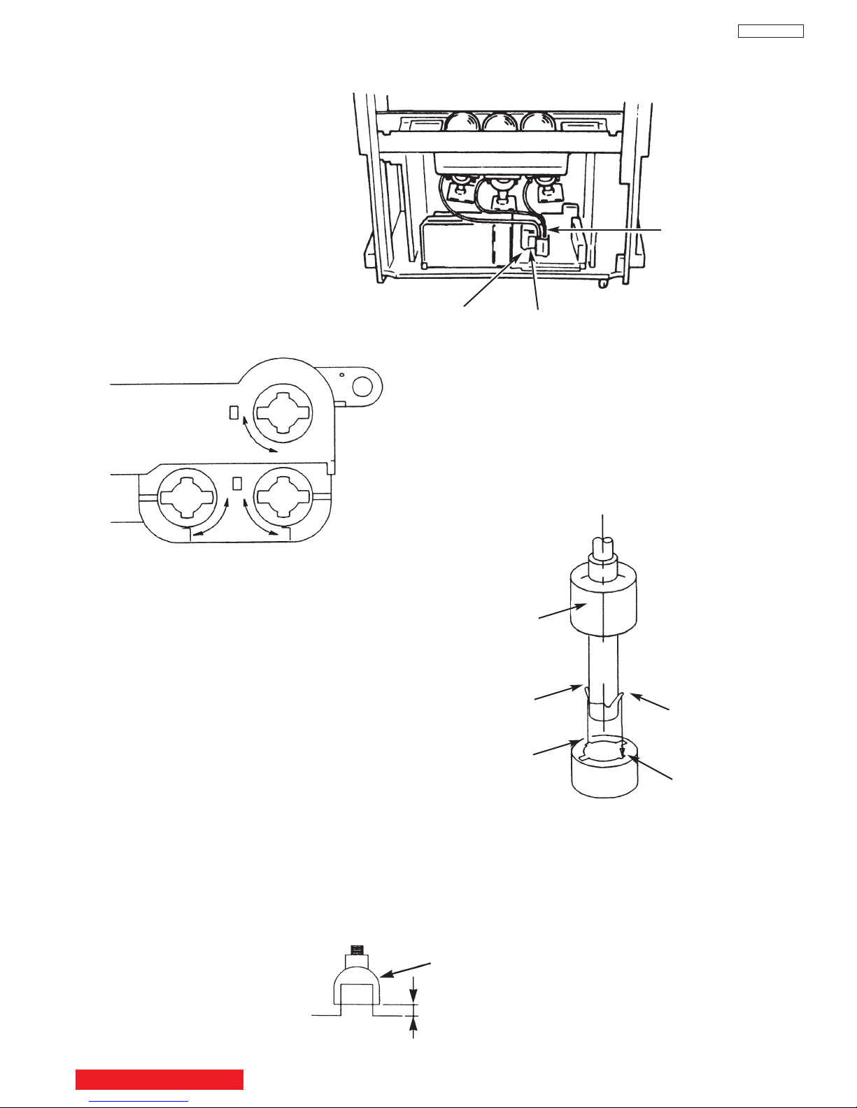
CAUTIONS WHEN CONNECTING / DISCONNECTING THE HV CONNECTOR
Perform the following when the
HV connector (anode connector)
is removed or inserted for CPT
replacement, etc.
Anode
connector
DP33KA/B
Deflection P.W.B.
PUSH
PUSH
Fig. A
3. Remove the connector slowly
by pulling it away from the
case.
FBT
During Removal
1. Roll out silicon cover from FBT’s contact area slowly.
2. While turning the connector about 90 degrees
following the arrow (0 position), push the connector
slightly towards the case. (Fig. A)
Silicon cover
Wing
Wing
During Insertion
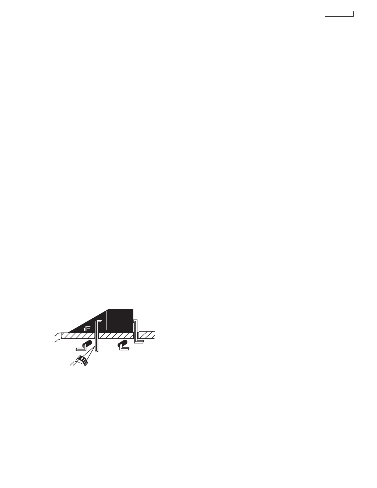
1. Please refer to direction for insertion as shown in Fig. B (L position). Insert connector until “CLICK” sound is heard.
e sure the connector is pressed r
Mak
2.
3. Confirm the contact by pulling the connector slightly. (Don’t pull hard because it may damage the connector).
4. Cover the high voltage output by carefully pushing silicon cover onto it. (Don’t turn the connector).
(REMARK)
1. Make sure the silicon cover is
covering the high voltage output.
TABLE OF CONTENTS
L Position
Fig. B
ight in, so that it has a good contact with the spr
Silicon Cover
less than 1mm
13
L Position
ing.
Page 14

GENERAL INFORMATION
INPUT 5
S-VIDEO
VIDEO
AUDIO
L/MONO
R
EXIT
INPUT
SELECT
MENU
VOL- VOL+ CH- CH+
E
FGH
c
f
a
b
d
g
e
CURSOR
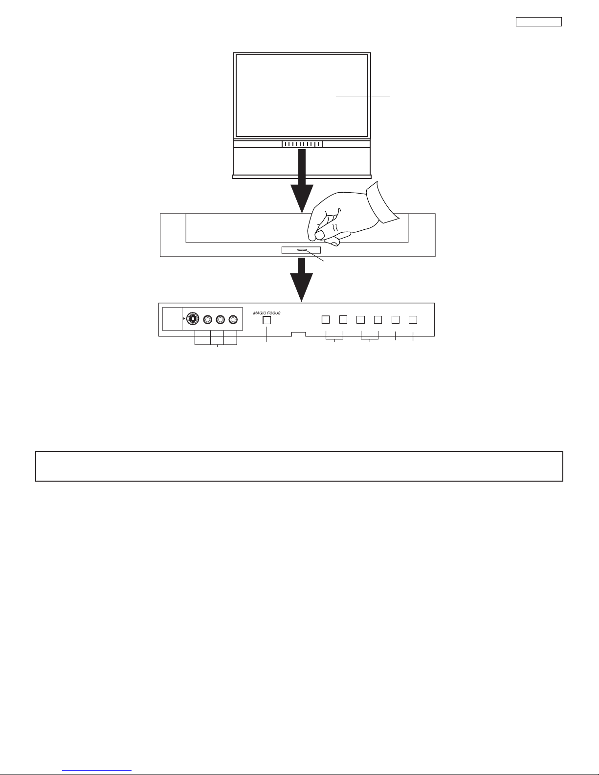
MAGIC
FOCUS
e
h
46F510
DP33KA/B
a MENU/SELECT button
This button allows you to enter the MENU, making it possible to set TV features to your preference without using the remote. This
button also serves as the SELECT button when in MENU mode.
b INPUT/EXIT button
Press this button to select the current antenna source, VIDEO: 1, 2, 3, 4, 5 or alternate antenna source. Your selection is shown in
the top right corner of the screen. This button also serves as the EXIT button when in MENU mode.
NOTES: Your remote control does not have an INPUT button. To change to video inputs, press VID1~VID5 buttons depending
on your choice.
c CHANNEL selector
Press these b
the cursor do
uttons until the desired channel appears in the top r
(
wn
H)
and up
(
uttons when in MENU mode
b
G)
.
ight cor
ner of the
TV screen.
These b
uttons also serve as
d VOLUME level
Press these buttons for your desired sound level. The volume level will be displayed on the TV screen. These buttons also serve
as the cursor left (
F) and right (E) buttons when in MENU mode.
e POWER button/POWER LED
Press this button to turn the TV on or off. This LED light is ON during normal operation.
f MAGIC FOCUS
Use this button to automatically adjust your picture quality to optimum performance. The Magic Focus button will not work when
adjustment mode is set to manual.
CKS (INPUT 5)
g FR
ONT INPUT J
A
Use these audio/video jacks for a quick hook-up from a camcorder or VCR to instantly view your favorite show or new recording.
Press the INPUT button until VIDEO: 5 appears in the top right corner of the TV screen. If you have mono sound, insert the audio
cable into the left audio jac
h IR RECEIVER Sensor
When using the remote control, point it towards the IR receiver for best response.
k.
TABLE OF CONTENTS
14
Page 15
GENERAL INFORMATION
INPUT 5
S-VIDEO
VIDEO
-
AUDIO-
L/MONO
R
EXIT
I
NPUT
SELECT
M
ENU
V
OL- VOL+CH- CH+
EF
G
H
c
f
a
b
d
g
POWER
PULL
e
h
46F500A
DP33KA/B
a MENU/SELECT button
This button allows you to enter the MENU, making it possible to set TV features to your preference without using the remote. This
button also serves as the SELECT button when in MENU mode.
b INPUT/EXIT button
Press this button to select the current antenna source, VIDEO: 1, 2, 3, 4, 5 or alternate antenna source. Your selection is shown in
the top right corner of the screen. This button also serves as the EXIT button when in MENU mode.
NOTES: Your remote control does not have an INPUT button. To change to video inputs, press VID1~VID5 buttons depending
on your choice.
c CHANNEL selector
Press these buttons until the desired channel appears in the top right corner of the TV screen. These buttons also serve as
the cursor down (H) and up (G) buttons when in MENU mode.
OLUME level
d V
olume level will be displayed on the TV screen. These buttons also serve
The v
el.
Press these b
uttons f
as the cursor left (
our desired sound le
or y
F) and r
ight (
uttons when in MENU mode.
E) b
v
e POWER button
Press this button to turn the TV on or off.
f MAGIC FOCUS
Use this button to automatically adjust your picture quality to optimum performance. The Magic Focus button will not work when
adjustment mode is set to man
ual.
g FRONT INPUT JACKS (INPUT 5)
or a quic
Use these audio/video jac
ks f
Press the INPUT button until VIDEO: 5 appears in the top right corner of the TV screen. If you have mono sound, insert the audio
cable into the left audio jack.
k hook-up from a camcorder or
VCR to instantly vie
w y
vorite show or new recording.
a
our f
h IR RECEIVER
The screen area acts as the IR receiver (remote sensor) of the TV. When using the remote control, point it towards the screen for
best response.
15
Page 16
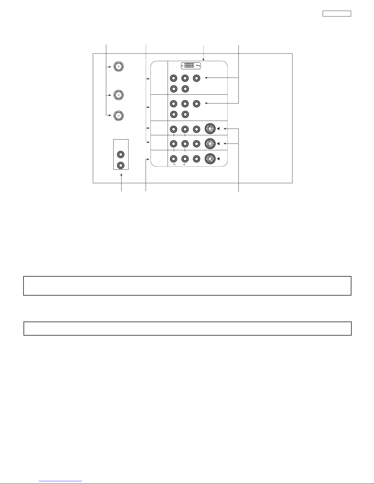
REAR PANEL JACKS
P
B
P
R
P
B
P
R
DVI-HDTV
ANT A
TO
CONVERTER
ANT B
L
AUDIO
TO HI-FI
R
b
a
d
e
f
g
c
Y
R
(MONO)/L
S-VIDEO
S-VIDEO
S-VIDEO
Y/VIDEO
R
(MONO)/L
R
(MONO)/L VIDEO
R
(MONO)/L VIDEO
R
L VIDEO
INPUT 1
INPUT 2
INPUT 3
INPUT 4
MONITOR
OUT
AUDIO
AUDIO
AUDIO
DP33KA/B
a Antenna Input/Output
The remote control allows you to switch between two separate 75-Ohm RF antenna inputs, ANT A and ANT B. ANT A input can
be displayed as a main picture or sub-picture. ANT B can only be displayed as a main picture. (ANT B cannot be displayed as a
sub-picture.) The antenna output labeled “TO CONVERTER” allows the ANT A connection to pass directly to a different source
such as a cable box, only when ANT B is displayed as a main picture.
b Audio/Video Inputs 1, 2, 3 and 4
The VID1~VID4 buttons will select each video source each time they are pressed. Use the audio and video inputs to connect
external devices, such as VCRs, camcorders, laserdisc players, DVD players etc. (If you have mono sound, insert the audio cable
into the left audio jack.)
NOTE: You may use VIDEO or S-VIDEO inputs to connect to INPUT 3 and 4, but only one of these inputs may be used at a
time.
c MONITOR OUT
These jac
output.
NOTE: S-VIDEO Output may be used for recording, only when the input is of S-VIDEO type.
d AUDIO TO HI-FI Output
These jacks provide variable audio output to a separate stereo amplifier. With this connection, the audio to the stereo can be
controlled by the television’s main volume.
e S-VIDEO Inputs 3 and 4
Inputs 3 and 4 provide S-VIDEO (Super Video) jacks for connecting equipment with S-VIDEO output capability.
ks provide fixed audio and video signals which are used for recording. Use the S-VIDEO Output for high quality video
16
Page 17

0
ANT
INFO
VOL CH
POWER
TV
CBL/SAT DVD/VCR
PIP
SWAP PIP MODE
FREEZE
DAY/NIGHT
MENU
MUTE
EXIT
LAST CH
REC
ASPECT
VIRTUAL HD
SELECT
SURF
VID1
VID2
VID3
VID4
VID5
CLU-4324UG: VIDEO
CLU-4328UG: DAY/NIGHT
DP33KA/B
REMOTE CONTROL
TABLE OF CONTENTS
17
Page 18
DP33KA/B
Color
Brightness
Contrast
Picture Mode
Video
Move
SEL
Select
Color Temperature
Sharpness
Tint
Reset Video Settings
Edge Enhancement
Setup
Locks
Aspect
Audio
Video
Move
SEL
Sel
Black Enhancement
Chan. Manager
100%
50%
50%
50%
High
ANT A/B
Middle
High
Day
Night
SEL
Select
Picture Mode Day
Night
Return
Next/Prev
MENU
SELECT
Video
Contrast 100% 50%
Brightness 50% 50%
Color 50% 45%
Tint Center Center
Sharpness 50% 50%
Color Temperature High Standard
Black Enhancement Middle Low
Edge Enhancement High Low
Auto Color Off Off
Noise Reduction Off Off
Color Management Off Off
(Set User Colors)
Auto Movie Mode Off Off
(TV/Cinema Detection)
Function Day Night Reset
Reset the video
menu settings on
current input to the
Day or Night
conditions depending
on the selected
VIDEO mode.
CUSTOMIZED PICTURE AND SOUND ADJUSTMENTS
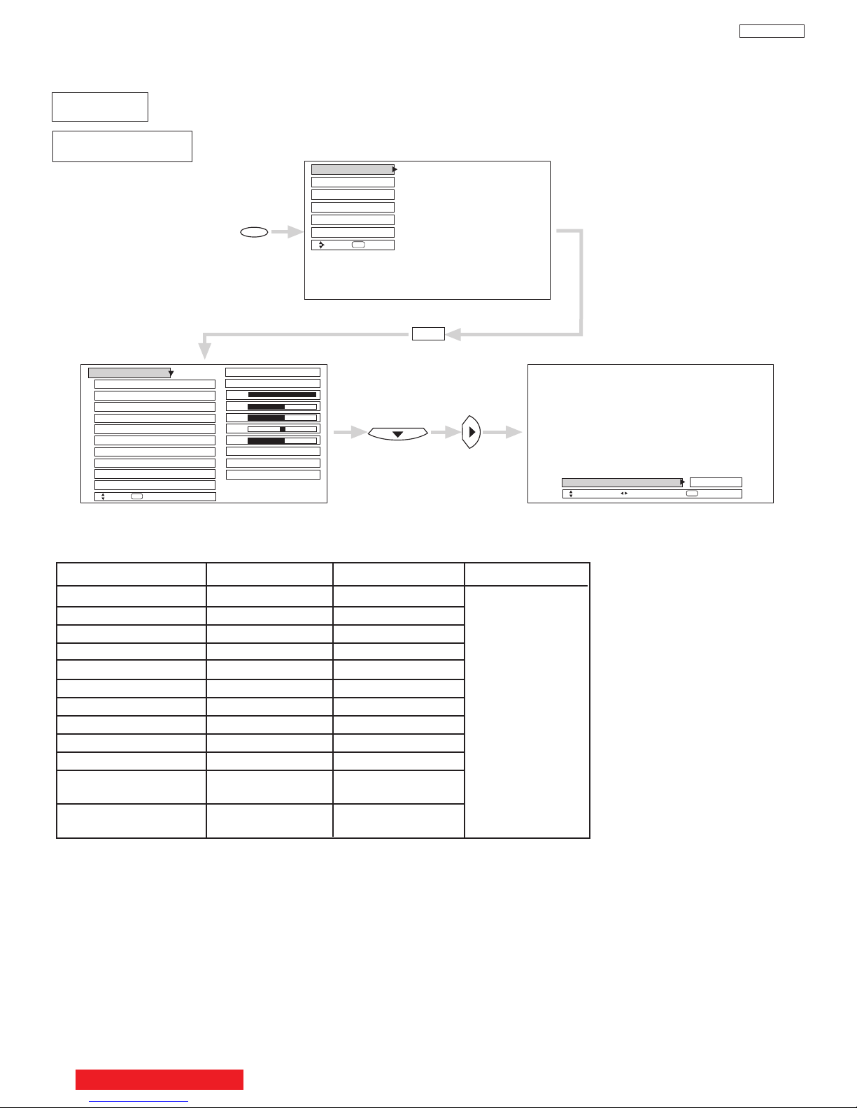
Select VIDEO to adjust picture settings and improve picture quality. You can independently customize each of the
Video Inputs to your preference to increase viewing performance and pleasure depending upon the video program
being viewed. If RESET is selected, only the selected input will reset to initial conditions.
Picture Mode
Use this function to choose from automatic picture settings to optimize your TV’s performance.
Use CURSOR F or E to highlight and select Picture Mode settings.
PICTURE MODE to return to previous menu.
TABLE OF CONTENTS
18
Press EXIT to quit menu or select
Page 19
CUSTOMIZED PICTURE AND SOUND ADJUSTMENTS
Color
Brightness
Contrast
Picture Mode
Video
Move
SEL
Select
Color Temperature
Sharpness
Tint
Reset Video Settings
Edge Enhancement
Setup
Locks
Aspect
Audio
Video
Move
SEL
Sel
Black Enhancement
Chan. Manager
100%
50%
50%
50%
High
ANT A/B
Middle
High
Day Night
MENU
SELECT
DP33KA/B
Use the CURSOR
G or H to highlight the function to be adjusted.
Press the SELECT button to select the function settings.
Press the CURSOR
F or E to adjust the function.
Press MENU to return to main menu.
Press EXIT to quit menu.
Contrast
Brightness
Color
Tint
Sharpness
Color Temperature
Use this function to change the contrast between black and white levels in the picture.
Use this function to adjust overall picture brightness.
Use this function to adjust the level of color in the picture.
Use this function to adjust flesh tones so they appear natural.
Use this function to adjust the amount of fine detail in the picture. Sharpness function will be disabled
when Noise Reduction is ON.
Set this to High for cooler color with more blue, set to Medium for more natural color, set to Standard for
accurate color or set to Black/White for more reddish color.
Black Enhancement
Use this function to enhance the shadow detail in dark scenes using the settings off, low, middle and high.
Edge Enhancement
Use this function to automatically enhance the edges between light and dark areas using the settings Off,
Low, Middle, and High.
NOTES: 1. If CONTRAST is selected, you are adjusting CONTRAST. The additional menu items BRIGHTNESS, COLOR, TINT,
and SHARPNESS can be selected and adjusted in the same manner.
2. Contrast will decrease automatically if stationary images such as digital still photos are left on the screen for more than
3 minutes.
3. It may be necessary to adjust TINT to obtain optimum picture quality when using the COMPONENT VIDEO Y-PBP
input jacks.
4. Ant A/Ant B have independent Video settings. Also, each of the video inputs have their own independent settings.
19
R
Page 20
CUSTOMIZED PICTURE AND SOUND ADJUSTMENTS
MAGIC
FOCUS
MAGIC FOCUS
Magic Focus Tune Up
Setup
Move
SEL
Return
Aligns the Red, Green, and Blue
colors to correct for Magnetic
Influences.
Auto
Manual
Setup
Locks
Chan. Manager
Aspect
Video
Move
SEL
Sel
Set The Inputs
Set The Clock
Menu Preference
Magic Focus Tune Up
Setup
Move
SEL
Select
Set Black Side Panel
Set Virtual HD
Set The Color System
Adjustment Mode
If you want to adjust now
Start
Audio
About Your TV
Set Closed Caption
Set Event Timer
MAGIC FOCUS
MENU
SELECT
SELECT
SELECT
DP33KA/B
Magic Focus
Tune Up
uto Digital Convergence Adjustment
A
Please turn ON your television for at least 20 minutes before using this feature.
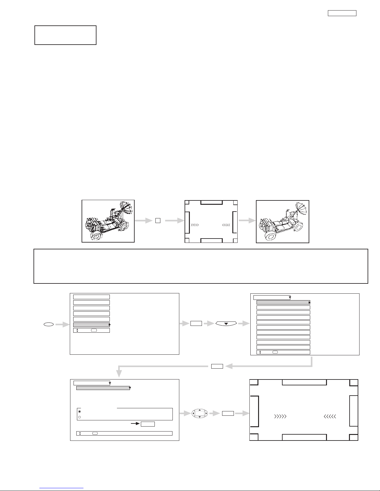
The Magic Focus button on control panel will not work when adjustment mode is set to Manual.
Your HITACHI Projection TV has three color projection tubes: one for red, one for green, one for blue. When mixed together in the proper
proportion, the output of these three color tubes can produce any color. To produce these colors, however, the beams must be precisely
aligned over each other so that the colors can be mixed. The process of aligning these picture beams is called “convergence”.
er a period of time, the picture tubes can drift out of alignment due to normal bumps and vibrations or moving the TV. If you move
Ov
your TV, or if, after a time, you notice color rings or halos around objects in the picture, you may want to converge (align) the colors.
Properly converged, the lines appear white, which is actually a combination of the outputs of the three color tubes. The output of the
green tube is stationary. The outputs of the red and blue tubes can be adjusted. When properly aligned, the outputs of all three tubes
should be directly over each other to produce the white lines.
To simplify convergence, HITACHI incorporates a function called MAGIC FOCUS located on the front control panel, which allows the TV
to self-adjust. Press this MAGIC FOCUS button and the convergence self adjustment will start and this process will take approximately
20 seconds. If this button is pressed during this process, no change in picture quality will occur. After this 20 second self-adjust period,
picture quality will be optimum (do not move the TV during self-adjust).
You may also select MAGIC FOCUS TUNE UP from the Setup Menu.
NOTES: Only a momentary press of the MAGIC FOCUS button is necessary to start AUTO DIGITAL CONVERGENCE. At any
time during this convergence correction process, you may press the MAGIC FOCUS button to exit the MAGIC FOCUS
mode. However, the convergence correction process needs to be completed to SAVE the new corrected convergence
data.
20
Page 21
CUSTOMIZED PICTURE AND SOUND ADJUSTMENTS
Setup
Locks
Chan. Manager
Aspect
Video
Move
SEL
Sel
Audio
Magic Focus Tune Up
Setup
Move
SEL
Return
Aligns the Red, Green, and Blue
colors to correct for Magnetic
Influences.
Auto
Manual
Adjustment Mode
If you want to adjust now
Start
Adjustment Point
Cursor
Set The Inputs
Set The Clock
Menu Preference
Magic Focus Tune Up
Setup
Move
SEL
Select
Set Black Side Panel
Set Virtual HD
Set The Color System
About Your TV
Set Closed Caption
Set Event Timer
MENU
SELECT
SELECT
SELECT
117 Manual Adjust
Please Enter Number.
0.Cancel and go to Normal Mode.
1.Done and go to Normal Mode.
2.Back to Adjust Mode
3.Factory Reset and back to
Adjust Mode.
0-3.Select
EXIT
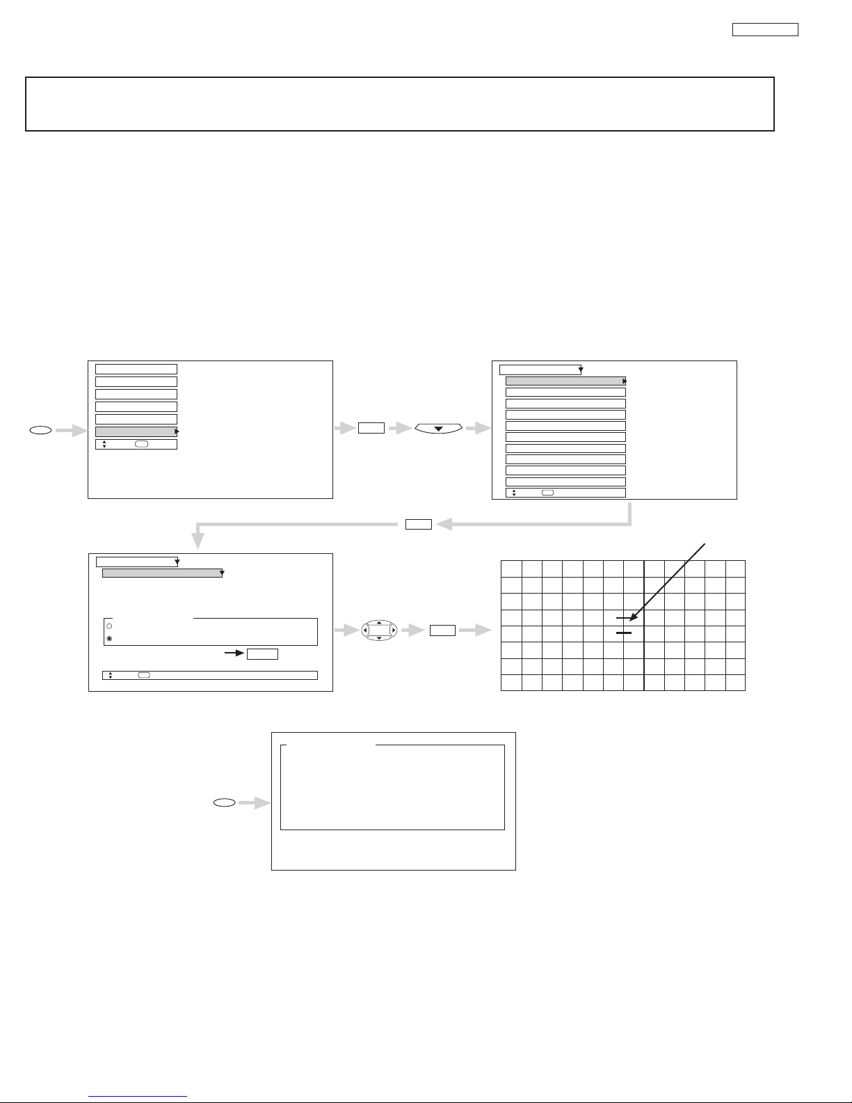
Manual Convergence Adjustment Mode
DP33KA/B
NOTES: 1. Please turn ON your television for at least 20 minutes before using this feature.
2. Auto Adjustment Mode is recommended. If convergence is still not acceptable, use the Manual Adjustment Mode.
3. If Auto Adjust mode is selected or the Magic Focus button is pressed, all manual adjust mode settings will be erased.
Using the Remote Control, select SETUP-MAGIC FOCUS TUNE UP-MANUAL ADJUSTMENT MODE-START to access convergence
crosshatch pattern. The adjustment point is indicated by the Adjustment Point Cursor.
To Move Adjustment Point
To move the adjustment point cursor using the CURSOR buttons, the Adjustment Cursor must be WHITE. Another way to move the
Adjustment Point Cursor is to press the following buttons: [2] up, [4] left, [5] down, [6] right. If you use the number buttons while the
adjustment point is WHITE, it will change to RED.
To Change the Color of Adjustment Point
Press the SELECT button repeatedly (WHITE-RED-BLUE-WHITE...). Green color is fixed and cannot be adjusted.
To Adjust the Convergence
Move the Adjustment Cursor to the point to be adjusted. Use the CURSOR to match the RED and BLUE colors to GREEN (reference
color). Properly aligned, all three colors should appear white.
If convergence is acceptable after Manual Convergence adjustment, press EXIT button to access menu mode.
Press the [0] button on the remote control to CANCEL adjusted data and return to main picture.
Press the [1] button on the remote control to SAVE adjusted data and return to main picture.
Press the [2] b
Press the [3] button on the remote control to recall the factory pre-set convergence data.
utton on the remote control to retur
n to the manual convergence adjustment mode (crosshatch pattern).
21
Page 22
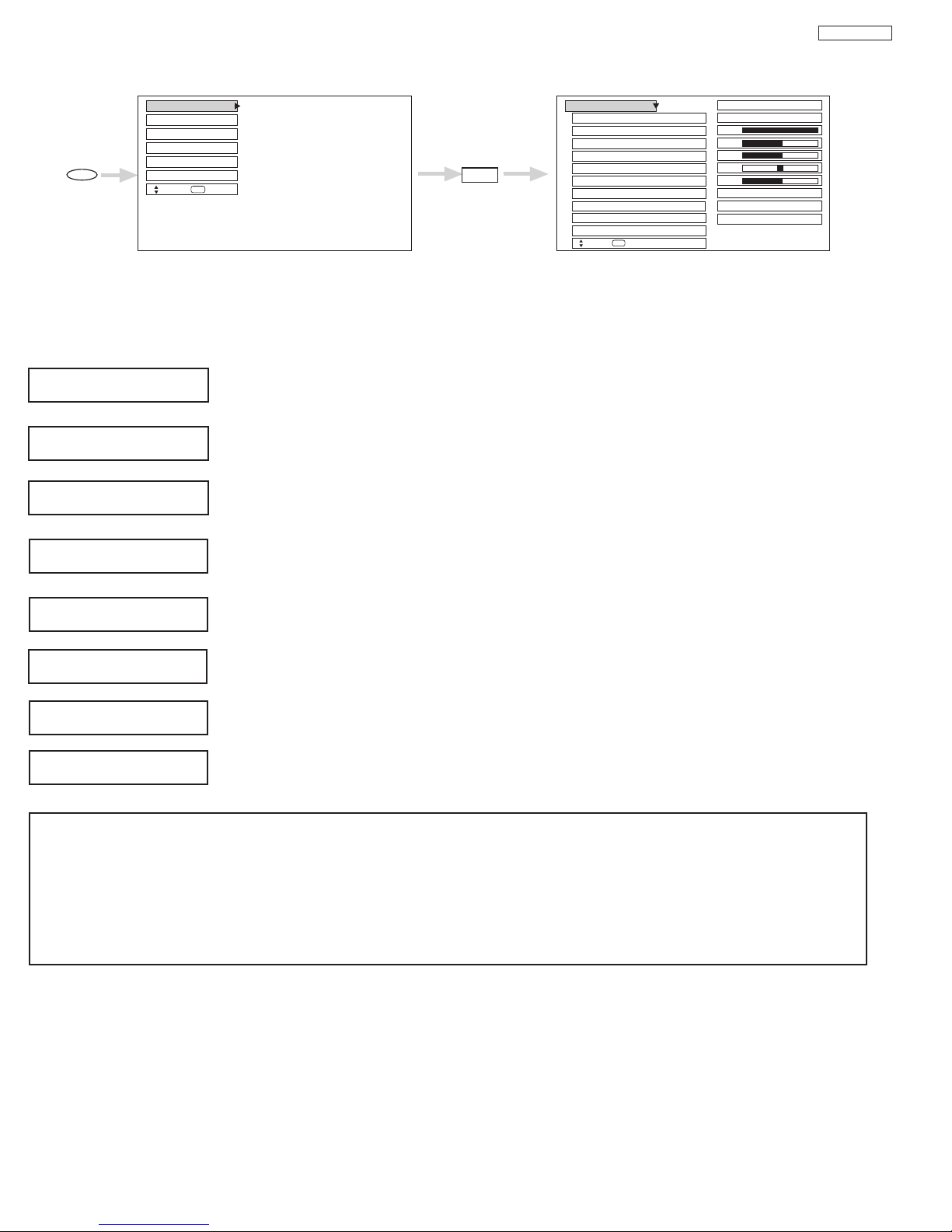
CUSTOMIZED PICTURE AND SOUND ADJUSTMENTS
Audio
Sound Enhancement
Balance
Bass
Treble
Audio
Move
SEL
Return
Internal Speakers
Audio Source
Perfect Volume
Auto Noise Cancel
50%
Off
On
Locks
Chan. Manager
Aspect
Audio
Video
Move
SEL
Sel
Setup
On
On
45%
LR
Stereo
Loudness
On
MENU
SELECT
Select AUDIO to adjust the TV to your preference and to improve the sound quality.
DP33KA/B
Press CURSOR
G, H, to select menu item.
Press CURSOR F or E to adjust the function.
Press EXIT to quit the MENU, or select Audio to return to the main menu.
NOTE: If TREBLE is selected you are adjusting treble. The additional menu items Bass and Balance can be selected and
adjusted in the same manner.
Treble
Bass
Sound Enhancement
Balance
Audio Source
This function controls the high frequency audio to all speakers.
This function controls the low frequency audio to all speakers.
This unction will reproduce the “live” sound you would hear in concert halls, sport stadiums, movie theaters,
etc. with only two speakers.
This function will control the left to right balance of the Projection TV internal speakers.
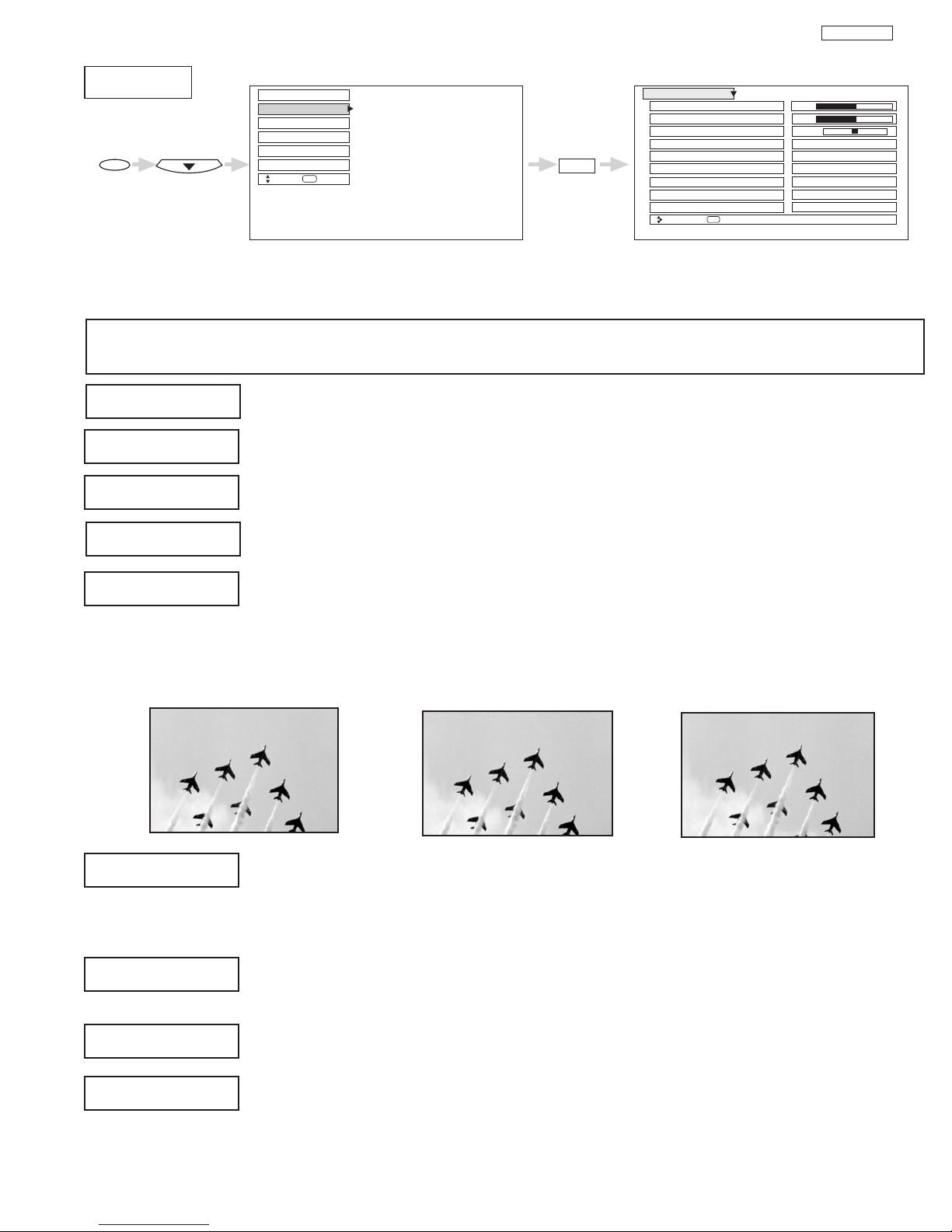
Multi-Channel Television Sound will allow you to select STEREO (a stereo broadcast), MONO (monaural
sound) used when receiving a weak stereo broadcast or 2nd Audio Prog (SAP) which may be a secondary
language, weather report, etc.
The sources received will be displayed at the top right edge of the TV. The source you select will be displayed
above the sources received. See example below for each selection when both stereo and second audio are
received (monaural is always received).
STEREO SELECTED
3:32 PM
Ant A 10
Stereo
R
SAP SELECTED
3:32 PM
Ant A 10
SAP
MONO SELECTED
3:32 PM
Ant A 10
Mono
R
R
Internal Speakers
This function is useful when setting up the external speakers.
ON - Select this f
OFF - Select this feature if you prefer to use only speakers from a separate stereo system.
Auto Noise Cancel
This function eliminates the noise between stations. If a channel is tuned and is noisy, this function will
automatically eliminate the audio f
Perfect Volume
This function will automatically adjust volume so each channel and input has the same average volume
level.
Loudness
This function tur
when listening at low volume levels.
eature if using the internal speakers only.
or that channel.
ns loudness ON or OFF
22
It will impro
.
v
e the quality of both lo
w and high frequency sounds
Page 23
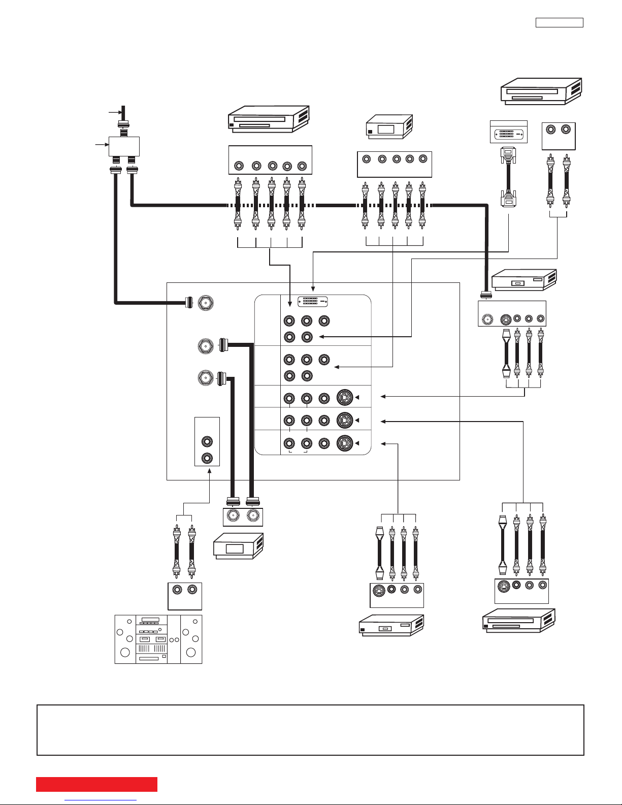
REAR PANEL CONNECTIONS
P
B
P
R
P
B
P
R
Outside antenna or
c
able TV coaxial cable
2-Way signal splitter
Stereo System Amplifier
LR
INPUT
Laserdisc player, VCR,
camcorder, etc.
H
DTV Set-Top Box
DVD Player
Cable TV Box
O
UTPUT
INPUT
VCR #1
ANT
IN
OUTPUT
S-VIDEO
VLR
ANT A
TO
CONVERTER
ANT B
L
Y
R
(MONO)/L
A
UDIO
TO HI-FI
R
S-VIDEO
S-VIDEO
S-VIDEO
Y/VIDEO
R
(
MONO)/L
R
(MONO)/L VIDEO
R
(
MONO)/L VIDEO
R
L VIDEO
INPUT 1
INPUT 2
INPUT 3
INPUT 4
M
ONITOR
OUT
OUTPUT
YP
B/CBPR/CR
L R
VCR #2
V L R
OUTPUT
S-VIDEO
V L R
INPUT
S-VIDEO
OUTPUT
Y P
B
P
R
L R
AUDIO
A
UDIO
AUDIO
DVI-HDTV
D-VHS
DIGITAL OUTPUT
L
R
OUTPUT
TYPICAL FULL-FEATURE SETUP
DP33KA/B
NOTE: 1.
Connect only 1 component to each input jack.
2. Follow connections that pertain to your personal entertainment system.
3. Composite video signal can be input to Input2~Input5.
4. Cables are not included with the purchase of this television.
TABLE OF CONTENTS
23
Page 24
y Picture Formats
4:3
INPUT
4:3 EXPANDED
4:3 ZOOM1
4:3 ZOOM2
16:9 STANDARD
4:3 STANDARD
INPUT
4:3 EXPANDED
4:3 ZOOM1
4:3 ZOOM2
16:9 STANDARD
4:3 STANDARD
INPUT
16:9
16:9 STANDARD 16:9 ZOOM
16:9 ZOOM
16:9 ZOOM
16:9
Displa
Press this button to quickly change the picture format ASPECT ratio.
DP33KA/B
Depending on the input signal, the picture f
4:3 Standard
4:3 Expanded use this aspect mode to display conventional (4:3) sources by linearly increasing image expansion from
Zoom1/Zoom2 Use these aspect modes to zoom in on conventional (4:3) sources.
4:3
16:9 Standard Use this aspect mode to display 16:9 sources like HDTV and DVD’s preserving the original 16:9 aspect
16:9 Zoom Use this aspect mode to zoom 16:9 images.
(1) NTSC/480i/480p Input
ormat ratio allows you to adjust the images through the following options.
Use this aspect mode to display conventional (4:3) images. Side panels (gray areas) are placed to the
left and right of the image to preserve the original aspect ratio of the source. Note: Use this mode for
only 15% of your total viewing time to prevent uneven aging of the phosphors. Phosphors in the lighted
area of the picture will age more rapidly than the black areas.
the center towards the edges of the display area in order to fill it.
ratio.
(2) 480i/480p INPUT
(3) 720p/1080i INPUT
NO
TE:
The Aspect Style setting y
ou
select for an ANT input will
automatically be set f
other ANT inputs
or the
ver,
e
w
Ho
.
all five video inputs have
independent Aspect Style
settings
.
TABLE OF CONTENTS
24
Page 25

DP33KA/B
SERVICE ADJUSTMENTS
TO GO TO AN ADJUSTMENT, CLICK ON ITS HEADING BELOW
1. ASSEMBLED P.W.B ADJUSTMENT..................................................................................................................26
1-1. Service Menu Access (NTSC, SDTV and HDTV) ..................................................................................26
1-2. Comb Filter Operation Check ................................................................................................................45
1-3. Video Settings Check..............................................................................................................................45
1-3-1. Color Temperature Check ............................................................................................................45
Black Enhancement......................................................................................................................45
1-3-2.
1-3-3. Edge Enhancement ......................................................................................................................45
1-3-4. Color Management ......................................................................................................................45
1-3-5. Color Coding ................................................................................................................................45
1-3-6. Auto Color ....................................................................................................................................45
1-3-7. Noise Reduction Check ................................................................................................................45
1-3-8. Auto Movie Mode Check ..............................................................................................................45
1-4. High Voltage Adjustment ........................................................................................................................46
2. FINAL ASSEMBLY ADJUSTMENT (Adjustment should be according to below order)..............................46
2-1. Cut Off Adjustment..................................................................................................................................46
2-2. DCU Phase Data Setting ......................................................................................................................46
2-3. Horizontal Position Adjustment (Coarse)................................................................................................47
2-4. Raster Tilt (Deflection Yoke)....................................................................................................................47
2-5. Beam Alignment......................................................................................................................................47
2-6. Raster Position........................................................................................................................................48
2-7. Vertical Size ..........................................................................................................................................48
2-8. Horizontal Size ......................................................................................................................................48
2-9. Beam Form ............................................................................................................................................49
2-10. Lens Focus..............................................................................................................................................49
2-11. Static Focus ............................................................................................................................................51
2-12. Digital Convergence ..............................................................................................................................51
2-12-1. Magic Focus Character Set Up ..................................................................................................52
2-12-2. Magic Focus Pattern Set Up ......................................................................................................53
2-12-3. Convergence Jig Screen Specification ......................................................................................53
2-12-4. Raster Position Adjsutment ........................................................................................................54
2-12-5. Convergence Point Adjustment ..................................................................................................54
2-12-6. Magic Focus Initialize..................................................................................................................55
2-13. Blue Defocus ..........................................................................................................................................59
2-14. White Balance ........................................................................................................................................59
2-15. Sub Brightness........................................................................................................................................60
2-16.
Sub-Picture Signal Amplitude Adjustment
2-17. Horizontal Position ................................................................................................................................62
2-18. Scanning Area Check ............................................................................................................................62
........................................................................................................................
ocus P
k
ack ....................................................................................................................64
2-19.
ADJUSTMENT POINT ........................................................................................................................................64
3.
3-1.
Raster Distor
CPT (R)(G)(B), F
tion Chec
3-2. Signal Block Assembly............................................................................................................................65
..............................................................................................................66
.
.B
3-3.
Main Chassis Deflection P
.W
3-4. Power Supply P.W.B. ..............................................................................................................................74
..............................................................................................61
63
*IMPORTANT
For many of the abo
generator, as well as the usual NTSC (480i) signal generator.
Hitachi recognizes that few companies offer HDTV or SDTV signal generators and that the cost of these generators is
sometimes prohibitive. For this reason, we suggest the use of a set-top-box for HDTV and SDTV adjustments. Usually,
there is a switch on the set-top-box which enables it to output HDTV (1080i or 720P) or SDTV (480P) signals even with
no input. In this case
TABLE OF CONTENTS
ve adjustments,
, the sync is automatically detected by the TV (at the Y-P
it is necessar
ve an HDTV (1080i or 720P) signal generator, SDTV (480P) signal
y to ha
Inputs on the rear panel).
BPR
25
Page 26

ASSEMBLED P.W.B. ADJUSTMENT
1.
1.1 Ser
vice Menu Access
Adjustment Procedure
(1) Press and hold INPUT key on Control Panel and then press POWER key on control panel to access I2C
adjustment mode.
(2) Receive signal on main picture. (NTSC, SDTV or HDTV).
Some menu pages have I2C adjustments for SDTV and HDTV. The set will automatically allow you to set
these items only when a SDTV or HDTV signal is input to the COMPONENT jacks on the back of the TV. ......
See table below.
(3) Check the OSD according to table on the following pages, using CURSOR G, H on Remote Control.
*: Adjustable Data
Others: Fixed Data (be careful not to change)
(4) Press EXIT key to exit I2C ADJUST mode.
NOTES: (1) If the TV I2C data is different from the I2C Parameter (of the following pages) for fixed data, change
the data.
(2) When exchanging microprocessor or EEPROM and TV is turned on for first time, it requires
2
initialization of Memory Initial of I
C adjustment menu. Press CURSOR E and hold for 3
seconds to initialize memory.
(3) Use FACTORY RESET to set TV to out of factory shipping conditions: Do not use MEMORY
INITIALIZE.
DP33KA/B
IMPORTANT: AFTER PERFORMING A FACTORY RESET OR A MEMORY INITIALIZATION, YOU MUST
UNPLUG THE AC CORD AND THEN PLUG IT BACK IN.
BACK TO ADJUSTMENTS
26
Page 27
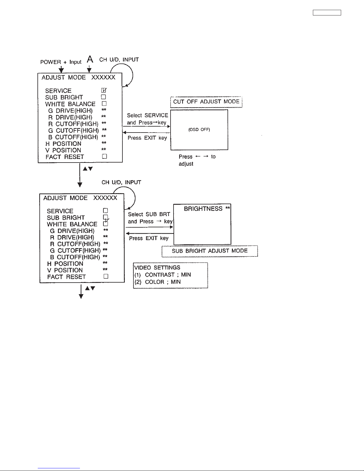
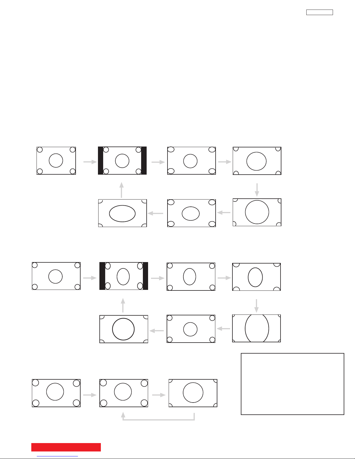
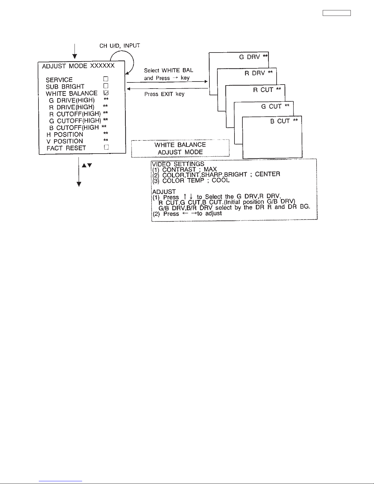
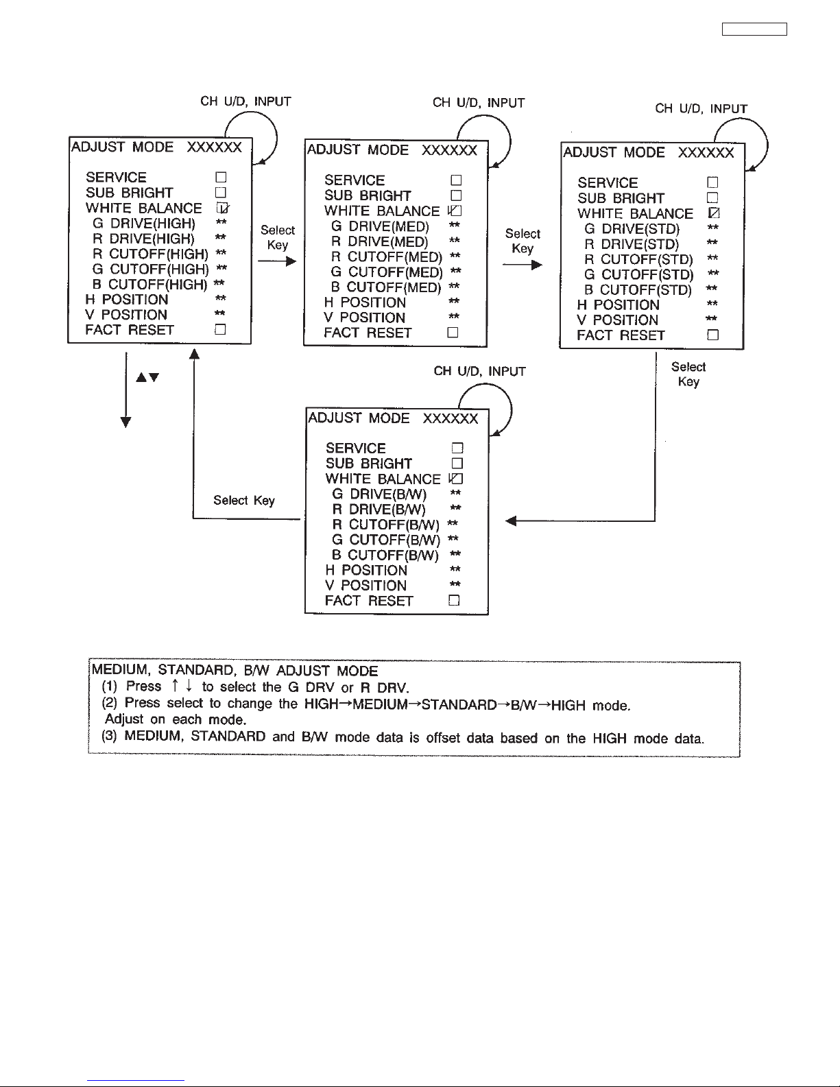
I2C OSD Flowchart
(a) Adjust Mode OSD
Press [POWER] + [INPUT] of Control Panel.
DP33KA/B
*: ADJUSTABLE ITEM
EXIT I2C ADJUST MODE
[EXIT] OR POWER on/off.
27
Page 28
(a) Adjust Mode OSD (continued)
DP33KA/B
28
Page 29
(a) Adjust Mode OSD (continued)
DP33KA/B
29
Page 30
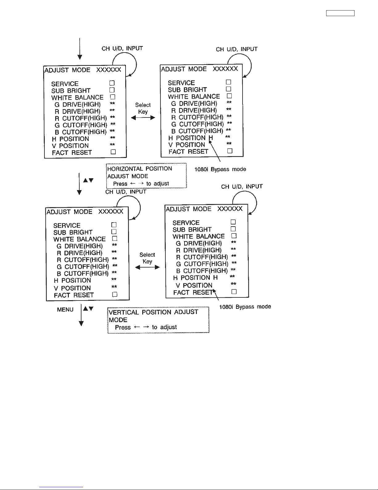
(a) Adjust Mode OSD (continued)
DP33KA/B
30
Page 31

DP33KA/B
(b) I2C Parameter List
Adjustment
Mode
OSD
Adjustment Item Adjustment
Ra
nge(HEX)
Initial
Data(HEX)
Adjustment
Value(HEX)
SERVICE SERVICE OFF
TA1360 (88H)
SUB BRIGHT Sub Brightness 3C~ FF 7F
WHITE BAL White Balance Mode (TA1360 88H)
High 3F
M
edium 49
Standard 4F
G DRIVE(HIGH)
G DRIVE(MED)
G DRIVE(STD)
G DRIVE (B/W)
Green Drive Gain Adjustment
00: .5 dB ~ 7F: +3dB
Data(M) = High + Medium - 3F
Data(S) = High + Standard - 3F
Data (B) = High + B/W - 3F
Black/White
00~ 7F
58
High 3F
Medium 4F
Standard 57
R DRIVE(HIGH)
R DRIVE(MED)
R DRIVE(STD)
R DRIVE (B/W)
Red Drive Gain Adjustment
00: .5 dB ~ 7F: +3dB
Data(M) = High + Medium - 3F
Data(S) = High + Standard - 3F
Black/White
00~ 7F
65
High 7F
Medium 7F
Standard 7F
R CUTOFF(HIGH)
R CUTOFF(MED)
R CUTOFF(STD)
R CUTOFF (B/W)
Red Cutoff Adjustment
00: 1.9 V~ FF: 2.9 V
Data(M) = High + Medium - 7F
Data(S) = High + Standard - 7F
Black/White
00~ FF
7F
High 7F
Medium 7F
Standard 7F
G CUTOFF(HIGH)
G CUTOFF(MED)
G CUTOFF(STD)
G CUTOFF (B/W)
Green Cutoff Adjustment
00: 1.9 V~ FF: 2.9 V
Data(M) = High + Medium - 7F
Data(S) = High + Standard - 7F
Black/White
00~ FF
7F
High 7F
Medium 7F
Standard 7F
B CUTOFF(HIGH)
B CUTOFF(MED)
B CUTOFF(STD)
B CUTOFF (B/W)
Blue Cutoff Adjustment
00: 1.9 V~ FF: 2.9 V
Data(M) = High + Medium - 7F
Data(S) = High + Standard - 7F
Black/White
00~ FF
7F
H POSITION Normal 40
H POSITION H
Horizontal Position Adjustment
00: .10%~ 7F: +10%
Data(H) = H POSI + H POSI H - 3F
Bypass
00~ 7F
49
FLEX
VD POSITION Vertical Position 00~ 7F 3F
FACTORY
RESET
TA13483-Sub (DAH)
SUB-CONT(TV-S) Sub Contrast Control
00: MIN(-3Db), 1F: MAX(+3Db)
00~ 1F 0F
OSD POSITION
H POSI OSD Horizontal Position 00~ FF 0D
V POSI OSD Vertical Position 00~ FF 22
CLK1 00~ 4F 40
CLK2 00~ 4F 40
CLK3 00~ 4F 49
CLK4
OSD Clock Adjust
00 4F 4F
AFC/CLOCK TEST - -
MEMORY INITIAL - -
I2C OPEN - -
IR BLASTER - -
~
31
Page 32

Adjustment
Mode OSD
Adjustment Item Adjustment
Range(HEX)
Initial
Data(HEX)
Adjustment
Value(HEX)
E2PROM edit
A
DRRESS ADRRESS - -
DAT
A DATA 00~ FF -
P MODE ADJ
Day Mode 00~ 60 60 Contrast Contrasrt Reset Step Adjustment
00 step (0%)
~ 60 step (100%)
Night Mode 00~ 60 30
Day Mode 00~ 60 30 Brightness Brightness Reset Step Adjustment
00 step (0%) ~ 60 step (100%)
Night Mode 00~ 60 30
Day
Mode 00~ 60 30
Color
Color Reset Step Adjustment
00 step (0%) ~ 60 step (100%)
Night Mode 00~ 60 27
Day Mode 00~ 60 30 Tint Contrast Reset Step Adjustment
00 step ~ 60 step
Night Mode 00~ 60 30
Day Mode 00~ 60 30 Sharpness Tint Reset Step Adjustment
00 step (0%) ~ 60 step (100%)
Night Mode 00~ 60 30
Day Mode High
Medium
Standard
Black/White
High
Color Temperature Color Temperature Reset Adjustment
High, Medium, Standard, Black/White
Night Mode High
Medium
Standard
Black/White
Standard
Day Mode High, Middle
Low, Off
Middle Black Enhancement Black Enhancement Reset Adjustment
High, Middle, Low, Off
Night Mode High, Middle
Low, Off
Low
Day Mode High, Middle
Low, Off
High
Edge Enhancement Edge Enhancement Reset Adjustment
High, Middle, Low, Off
Night Mode High, Middle
Low, Off
Low
DIGITAL MODULE HDTV Model only - -
HFRQ-N The number of times of Sync Frequency 00~ 0F 03
INPUT1 Input1 YPBPR Horizontal Frequency Detection Select
00: Auto, 01: 480i, 02: 480p, 03: 720p, 04: 1080i
00~ 04 00
INPUT2 Input2 YPBPR Horizontal Frequency Detection Select
00: Auto, 01: 480i, 02: 480p, 03: 720p, 04: 1080i
00~ 04 00
V CHIP/ CCD
SAMPL ING 00~ FF 00
POLLING 00~ FF 0F
START 00~ 07 02
TIMEOUT 00~ 1E 05
STATUS
V Chip Adjust
00~ 07 02
CLK POS
Adjust CCD Clock Position
HDTV only
00~ 1F 0A
VIDEO ID VIDEO ID Detection
0: 4:3 signal, 1: 4:3 letter box signal
2: 16:9 screen signal, FF: No VIDEO ID
00~ 02, FF *
IR BLASTER
WAIT IR Blaster Adjustment 00~ FF 06
REPEAT 00~ FF 20
(b) I2C Parameter List (continued)
DP33KA/B
32
Page 33

Adjustment
Mode OSD
Adjustment Item Adjustment
Range(HEX)
Initial
Data(HEX)
Adjustment
Value(HEX)
ISF Mode: TA1360 (88H)
RGBOUT
0 RGB Output Mode Switch
00: Normal, 01: R only
, 02: G only, 03: B only
00
~ 03 00
SUB-BRT Brightness Adjustment
00: .40 IRE~ FF: +40 IRE
DVI Input Data=SUB-BRT + SUBBRTH-7H
3C~ FF 7F
G-DRV-H High 3F
G
-DRV-M Medium 49
G-DRV-S Standard 4F
G-DRV-B
Green Drive Gain Adjustment
00: -5 dB ~
7F: +3dB
Data(M) = High + Medium - 3F
Data(S) = High + Standard - 3F
Black/White
00~ 7F
58
R-DRV-H High 3F
R-DRV-M Medium 4F
R-DRV-S Standard 57
R-DRV-B
Red Drive Gain Adjustment
00: -5 dB ~ 7F: +3dB
Data(M) = High + Medium - 3F
Data(S) = High + Standard - 3F
Black/White
00~ 7F
65
R-CUT-H High 7F
R-CUT-M Medium 7F
R-CUT-S Standard 7F
R-CUT-B
Red Cutoff Adjustment
00: 1.9 V~ FF: 2.9 V
Data(M) = High + Medium - 7F
Data(S) = High + Standard - 7F
Black/White
00~ FF
7F
G-CUT-H High 7F
G-CUT-M Medium 7F
G-CUT-S Standard 7F
G-CUT-B
Green Cutoff Adjustment
00: 1.9 V~ FF: 2.9 V
Data(M) = High + Medium - 7F
Data(S) = High + Standard - 7F
Black/White
00~ FF
7F
B-CUT-H High 7F
B-CUT-M Medium 7F
B-CUT-S Standard 7F
B-CUT-B
Blue Cutoff Adjustment
00: 1.9 V~ FF: 2.9 V
Data(M) = High + Medium - 7F
Data(S) = High + Standard - 7F
Black/White
00~ FF
7F
SUBCNT0 Sub Contrast 00: -3.4 dB ~ 1F: +2.6 dB 00~ 1F 12
COLOR-3 TV/NTSC 4D
COLOR-D SDTV 4D
COLOR-E
Color
(Center Adjustment)
00: -20 dB ~ 7F: +4.5 dB
HDTV
00~ 7F
52
COLOR-M Medium 1F
COLOR-S Standard 1F
COLOR-B
Color Offset
B/W
00~ 3F
1F
TINT-3 TV/NTSC 41
TINT-D SDTV 41
TINT-E
Tint(Center Adjustment)
00: -32 degree
7F: +32 degree
HDTV
00~ 7F
43
TINT-M Medium 1F
TINT-S Standard 1F
TINT-B
Tint Offset
B/W
00~ 3F
1F
SHARP-3 ANT A, B/NTSC 20
SHARP-G 480i/480p 20
SHARP-I 720p/1080i 1F
SHARP-9 Photo MC 1F
SHARP-C
Sharpness
(Center Adjustment)
-10 dB ~ +15 dB
SPLIT
00~ 7F
20
(b) I2C Parameter List (continued)
DP33KA/B
33
Page 34

Adjustment
Mode OSD
Adjustment Item Adjustment
Range(HEX)
Initial
Data(HEX)
Adjustment
Value(HEX)
ISF
Mode: TA1360 (88H)
RY-PH3
ANT A, B/NTSC 00
RY-PHD SDTV 00
RY-PHE
R-Y/B-Y Phase
00: 90 degree
0F
: 109 degree
HDT
V
00
~0F
0
0
R
/BGA3H High 0A
R/BGA3M Medium 08
R/BGA3S Standard 06
R/BGA3B
TV
/NTSC
Black/White 03
R/BGADH High 0A
R/BGADM Medium 08
R/BGADS Standard 06
R/BGADB
SDTV
Black/White 03
R/BGAEH High 08
R/BGAEM Medium 06
R/BGAES Standard 04
R/BGAEB
R-Y/B-Y Gain
00: 0.56
0F
: 0.86
HDTV
Black/White
00~ 0F
03
GY-PH-4 TV/NTSC 02
GY-PH-F SDTV 02
GY-PH-G
G-Y/B-Y Phase
00: 232.5 degree
0F: 255 degree
HDTV
00~ 0F
03
G/BGA3H High 02
G/BGA3M Medium 03
G/BGA3S Standard 04
G/BGA3B
TV/NTSC
Black/White 05
G/BGADH High 02
G/BGADM Medium 03
G/BGADS Standard 04
G/BGADB
SDTV
Black/White 05
G/BGAEH High 00
G/BGAEM Medium 00
G/BGAES Standard 00
G/BGAEB
G-Y/B-Y Gain
00: 0.3
0F: 0.45
HDTV
Black/White
00~ 0F
00
DC-PNT0 DC Restoration Point 00: 0% ~ 07: 47% 00~ 07 00
DCRATH High 00
DCRATM Middle 00
DCRATL Low 00
DCRATO
DC Restoration Rate
00: 100% ~ 07: 135%
Black
Enhancement
Off
00~ 07
00
DC-LMT0 DC Restoration Limit Point
00: 60%, 01: 73%, 02: 87%, 03: 100%
00~ 03 00
DABLPN0 Dynamic ABL Detection Point
00: MIN ~ 03: MAX
00~ 03 03
DABLGAH High 00
DABLGAM Middle 00
DABLGAL Low 00
DABLGAO
Dynamic ABL Gain
00: MIN ~ 03: MAX
Black
Enhancement
Off
00~ 03
00
(b) I2C Parameter List (continued)
DP33KA/B
34
Page 35

Adjustment
Mode
OSD
Adjustment Item Adjustment
Ra
nge(HEX)
Initial
Data(HEX)
Adjustment
Value(HEX)
TA1360 (88H)
DIMMER Not use 00~ 3F *
CONTRAST Not use 00~ 7F *
SCP-SW0 Sand castle Pulse Switch
00: Internal, 01: External Input
00~ 01 01
H-POSI Normal 40
H-POSIH Bypass 49
H-POSIS
Horizontal Position Adjustment
00: -10%~ 7F: +10%
Data(H) = H POSI + H POSI H - 3F
DVI=SAM 1080i Bypass,
Data(S) = H POSI + H POSI H - 3F
+
H-POSIS - 3F
SAM-1080i Bypass
00~ 7F
37
APRTR-3 ANT A, B/NTSC 01
APRTR-G 480i/480p 01
APRTR-I 720p/1080i/PhotoMC 00
APRTR-C
Aperture Control Peak f0
0: 15 MHz, 1: 8.8 MHz
2: 7.5 MHz, 3: 5 MHz
SPLIT
00~ 03
01
CLT-0 Color Limiter Level Switch
0: 1.65 Vp-p, 1: 2 Vp-p
00~ 01 01
CSRTG-0 Color SRT Gain
0: min~ 3: max
00~ 03 00
CSRTF-0 Color SRT Frequency
0: 4.3 MHz~ 1: 5.8 MHz
00~ 01 01
VSM-PHP ANT A, B, NTSC/480i/480p 06
VSM-PHJ
VM Phase
00: -37.5 ns, 05: Normal
07: +15 ns
720p/1080i/ANT C/PhotoMC
00~ 07
04
CDE-0 Color Detail Enhancer
00: min ~ 03: max
00~ 03 00
DCUBRT0 RGB Brightness 00: -20 IRE ~ 7F: +20 IRE 00~ 7F 3F
DCUCNT0 RGB Contrast 00: -17 dB ~ 7F: 0 dB 00~ 7F 5A
OSDACL0 OSD Auto Contrast Limiter Switch 0: OFF 1: ON 00~ 01 00
OSDBRT0 OSD Brightness Adjustment
00: 5 IRE, 01: 0 IRE, 02:-5 IRE, 03:-10 IRE
00~ 03 02
OSDCNT0 OSD Contrast Adjustment
00: -9.5 dB ~ 03: 0 dB
00~ 03 02
DCRRSW0 DC Restoration Ratio Switch
0: 100% less, 1: 100% over
00~ 01 00
COLORG0 Color Correction Point
00: OFF, 01: 0.23 Vp-p, 02: 0.37 Vp-p, 03: 0.52 Vp-p
00~ 03 00
YCGA-0 Component Dynamic Y/C Correction Select
00: OFF, 01: min, 02: mid, 03: max
00~ 03 00
APL/BS0 APL / Black Stretch Start Point
00: 0 IRE ~ 03: 23 IRE
00~ 03 00
BLC-0 Black Level Auto Correction Switch
00: OFF, 01: ON
00~ 01 00
BDL-0 Black Detection Level Switch
00: 3 IRE, 1: 0 IRE
00~ 01 00
BSARE0 Black Stretch Area Correction Switch
00: ON, 01: OFF
00~ 01 01
SRTGA-0 SRT(Super Real Transient) Gain
00: MIN ~ 1F: MAX
00~ 1F 10
(b) I2C Parameter List (continued)
DP33KA/B
35
Page 36

Ad
justment
Mode
OSD
A
djustment Item Adjustment
Ra
nge(HEX)
Initial
Data(HEX)
Ad
justment
Value(HEX)
TA1360 (88H)
WPLLVL-0 White Character Correction Amplitude
00: min ~ 07: max
00~ 07 07
ABLPN0
ABL Detection Point
00: MIN
~ 07: MAX
00
~ 07 07
ABLGA0 ABL Gain
00: MIN ~ 07: MAX
00~ 07 00
DGGAIN0
Dynamic Y Gamma Gain vs Dark Area
00: OF
F ~ 07: MAX(+6 dB)
00
~ 03 00
DGAREA0 Dynamic Y Gamma Gain vs Bright Area
00: OFF ~ 07: max
00~ 07 00
STATG10 Static Y Gamma Black Gain
00: OFF, 01: MIN(0 DB) ~ 07: MAX(+6 DB)
00~ 07 00
STATG20 Static Y Gamma Bright Gain
00: OFF, 01: MIN(0 DB) ~ 03: MAX(-6 DB)
00~ 03 03
YOUTG-0 Y Gamma Switch
0: OFF, 1: ON
00~ 01 00
YDTL-0 Y Detail Control
00: MIN(Trap) ~ 0F: MAX(+6 dB)
00~ 0F 07
YDELAY0 Y Group Delay Control
00: MIN(Trap) ~ 0F: MAX(+6 dB)
00~ 0F 09
WPPNT0 White Peak Blue Point
00: 55 IRE ~ 07: 105 IRE
00~ 07 00
WPGA-0 White Peak Blue Gain
00: min(+2 dB) ~ 07: max(+9.5 dB)
00~ 07 00
HIBRT0 High Bright Color Switch
00: OFF, 01: ON
00~ 01 00
WPS-0 White Peak Suppressor Level
00: 110 IRE, 01: 130 IRE
00~ 01 01
BLS-0 Blue Stretch Gamma Correction
00: OFF, 01: ON
00~ 01 00
GSTR-0 Green Stretch
00: OFF ~ 03: MAX
00~ 03 00
BSTRG-0 Blue Stretch Gain
00: OFF ~ 03: MAX(+4 dB)
00~ 03 00
BSTRP-0 Blue Stretch Point
00: MIN(30 IRE)~ 03: MAX(45 IRE)
00~ 03 00
BSCHR10 Black Stretch Characteristic Switch 1
(OFF~ MAX)
00~ 01 00
BSCHR20 Black Stretch Characteristic Switch 2
(OFF~ MAX)
00~ 01 00
(b) I2C Parameter List (continued)
36
DP33KA/B
Page 37

Ad
justment
Mode OSD
A
djustment Item Adjustment
Range(HEX)
Initial
Data(HEX)
Ad
justment
Value(HEX)
UPD64084 (B9H) Read Mode
SYNCDET
Sync Detection
0: Sync, 1: No Sync
00
~ 01 *
F
-STD Frame Sync Nonstandard Detection
0: Standard, 1: Non standard
00
~ 01 *
V-STD Vertical Sync Nonstandard Detection
0: Standard, 1: Non standard
00~ 01 *
H-ST
D Horizontal Sync Nonstandard Detection
0: Standard, 1: Non standard
00
~ 01 *
NOISE Noise Level Detection
00: Noise Small ~ FF: Noise Large
00~ FF *
VID-ID Video ID Detection
0: 4:3 signal, 1: 16:9 signal, 2: 4:3 letter box signal
00~ 03 *
UPD64084 (B8H)
DYGA Y Motion Detection Gain
0: Gain 0 ~ F: Gain MAX
00~ 0F 09
DCGA Chroma Motion Detection Gain
0: Gain 0 ~ F: Gain MAX
00~ 0F 06
VAPGA Vertical Aperture Control Gain
0: Correction OFF ~ 7: Correction MAX (x0.875)
00~ 07 00
VAPIN Vertical Aperture Control Invert
0: Correction OFF ~ 1F: Correction MAX (x0.875)
00~ 1F 0B
YHCOR Y Output High Frequency Coring
0: Coring OFF, 1: Coring Small, 2: Coring Center, 3: Coring
Large
00~ 03 00
TA1383F-Main (D9H) Read Mode
HSYNC-M Horizontal Sync Number
NTSC/480i = 22, 480p = 43, 1080i = 48, 720p = 60
00~ FF *
VSYNC-M Vertical Sync Number
60Hz = 5E
00~ 7F *
CSYNC-M SYNC Mode Detection
0:2 Level Sync, 1:3 Level Sync
00~ 01 *
TA1383-Sub (DBH) Read Mode
HSYNC-S Horizontal Sync Number
NTSC/480i = 22, 480p = 43, 1080i = 48, 720p = 60
00~ FF *
VSYNC-S Vertical Sync Number
60Hz = 5E
00~ 7F *
CSYNC-S SYNC Mode Detection
0:2 Level Sync, 1:3 Level Sync
00~ 01 *
(b) I2C Parameter List (continued)
37
DP33KA/B
Page 38

DP33KA/B
Adjustment
Mode OSD
Adjustment Item Adjustment
Range(HEX)
Initial
Data(HEX)
Adjustment
Value(HEX)
TA1383-Main/Sub (D8H)
CONTM1 Main TA1383 ANT A, B 10
CONT
S1 Sub TA1383 ANT A 10
CONT
-2 NTSC 10
CONT-K ANT C/YPBPR/DVD/BM 10
CONT-A
Sub Contrast Control
00: MIN(-3dB)
1F: MAX(+3dB)
DVI
00~ 1F
10
CLRM1 Main ANT A, B 10
CLRS1 Sub ANT A 10
C
LR-2 NTSC 10
CLR-K ANT C/YPBPR/DVD/BM 10
CLR-A
Sub Color Control
00: MIN(-3dB)
1F
: MAX(+3dB)
DVI
00~ 1F
10
TINTM1 Main ANT A, B 08
TINTS1 Sub ANT A 08
TINT-2 NTSC 08
TINT-K ANT C/YPBPR/DVD/BM 08
TINT-A
Sub Tint Control
0: MIN(-7deg)
F: MAX(+7deg)
DVI
00~ 0F
08
TA1383-Main/Sub (D8H/DAH)
BANDW-F ANTA, B/NTSC/480i 01
BANDW-5 480p 02
BANDW-6 720p 00
BANDW-7 1080i 00
BANDW-9 PhotoMC 00
BANDW-C
Band Width Filter Switch
0: OFF, 1: 4.2MHz, 2: 11.3MHz, 3: Mute
SPLIT
00~ 03
01
YDL1-F ANTA, B/NTSC/480i 01
YDL1-5 480p 01
YDL1-6 720p 01
YDL1-7 1080i 01
YDL1-9 PhotoMC 01
YDL1-C
Y Delay Time Adjust 1
Base Band Section
0: -10 ns, 1: 0 ns
2: +10 ns, 3: +20 ns
SPLIT
00~ 03
01
Y-DL2-0 Y Delay Time Adjust 2 NTSC Section
1: +40 ns, 2: +80 ns, 3: +120 ns
00~ 03 00
AFCRAN0 Horizontal AFC Switch
0: Normal, 1: Narrow
00~ 01 00
FDET-3 Frequency Detection Input Switch
0: 480i-1 • • • NTSC, 1: 480i-2 • • • NTSC
2: D-SYNC2, 3: HD/VD
00~ 03 00
HSEPL-3 ANT A, B/NTSC 00
HSEPL-4 480i 00
HSEPL-5 480p 00
HSEPL-J
Horizontal Sync Separation
Level Switch
0: 20%, 1: 27%, 2: 34%, 3: 40%
720p/1080i/ANT C
00~ 03
00
VSEPL-3 TV/NTSC 00
VSEPL-4 480i 00
VSEPL-5 480p 00
VSEPL-J
Vertical Sync Separation Level switch
0: 40%, 1: 50%, 2: 60%, 3: 70%
720p/1080i/ANT C
00~ 03
00
DSEPL-G 480i/480p 00
DSEPL-J
D-SYNC2-IN Sync Separation Level Switch
0: 20%, 1: 30%, 2: 40%, 3: 50%
720p/1080i/ANT C
00~ 03
00
AFCMD-1 ANT A, B 02
AFCMD-2 NTSC 02
AFCMD-L
AFC Gain Switch
0: AUTO 1, 1: AUTO 2, 2: AUTO 3,
3: AUTO 4, 4: +6dB, 5: 0 dB, 6:-12dB
7: OFF(Horizontal Free Run)
ANT C/YPBPR/DVD
00~ 07
04
VMODE-0 Vertical Sync Mode Switch
0: Normal PLL Mode, 1: Sync Output Mode
ANT A, B/NTSC 00~ 01 00
48ISEP3 480i Separator Mode Switch
0: ON, 1: OFF
ANT A, B/NTSC 00~ 01 00
HDPOSI3 ANT A, B/NTSC 06
HDPOSI4 480i 05
HDPOSI5 480p 00
HDPOSI6 720p 09
HDPOSI7
HD Output Phase Adjustment
0: 800 ns Advance, F: Sync Center
1080i
00~ 0F
07
(b) I2C Parameter List (continued)
38
Page 39

DP33KA/B
Adjustment
Mode OSD
Adjustment Item Adjustment
Range(HEX)
Initial
Data(HEX)
Adjustment
Value(HEX)
NJW
1160/61 82H
BBE-LO BBE Low Frequency Effect Level
0dB~ 15dB
00~ 0F 07
BBE-HI BBE High Frequency Effect Level
0dB
~ 15dB
00~ 0F 05
AGC AGC Level Setting
150m/300m/400m/540mVrms
00~ 03 01
Adjustment
Mode
OSD
Adjustment Item Adjustment
Ra
nge(HEX)
Initial
Data(HEX)
Adjustment
Value(HEX)
FC-4 Read Mode
FC-VER FC Unit Micro Version Number 00~ FF *
FC-CHKH FC Unit Micro Check Sum Number (High Bit) 00~ FF *
FC-CHKL FC Unit Micro Check Sum Number (Low Bit) 00~ FF *
3-2T/C TV/Cinema: 3-2 Pull Down Signal Detection
0: TV, 1: Cinema
00~ 01 *
VFREQH 00~ FF *
VFREQL
Main/Sub Vertical Frequency Detection (High 6Bit, Low 8Bit)
59.94Hz = 17D2, 60Hz = 17CC
00~ FF *
HFREQH 00~ FF *
HFREQL
Main/Sub Vertical Frequency Detection (High 5Bit, Low 8Bit)
NTSC/480i = 0E85, 480p = 0742
1080i = 06C2, 720p = 0514
00~ FF *
APLDET APL Detection 00~ FF *
PEAKDET PEAK Detection 00~ FF *
YGAIN Dynamic Contrast Y Gain 00: x1, 7F: x2 00~ 7F *
CGAIN Dynamic Contrast Color Gain 00: x1, 3F: x2 00~ 3F *
FC-4 Write Mode
B-BACK Blue Back: FC Free Run Mode
0: Blue Back OFF, 1: Blue Back ON
00~ 01 *
MAININ Main Input Mode
0: NTSC, 1: 480i, 2: 480p, 3: 720p, 4: 1080i, 5: BM
00~ 0F *
SUBIN Sub Input Mode
0: NTSC, 1: 480i, 2: 480p, 3: 720p, 4: 1080i
00~ 0F *
VDPOS-0 VD Position Offset 00~ 7F 3F
LINE-I0 Line Interpolation 0: OFF, 1: ON 00~ 01 00
M-SLOPE Sat Slope 1 (Magenta) -90˚ (00h)~ 0˚ (40h)~ 90˚ (FFh)
Data=M-SLOPE+M-Menu- 30(1Eh)
00~ 7F 40
M-HUEW Hue Width 1 (Magenta)
Data= Width /360˚ x256=90˚ /360˚ x256=64 (3Fh)
00~ 3F 3F
M-HUECH Hue Center 1 (Magenta) High Bit 00~ 03 00
M-HUECL Hue Center 1 (Magenta) Low Bit
Data= Hue /360˚ x1024=45˚ /360˚ x1024=128 (0080h)
00~ FF 80
M-CLIP Sat Clip 1 (Magenta) 00~ FF FF
R-SLOPE Sat Slope 2 (Red) -90˚ (00h)~ 0˚ (40h)~ 90˚ (FFh)
Data=R-SLOPE+R-Menu- 30(1Eh)
00~ 7F 40
R-HUEW Hue Width 2 (Red)
Data= Width /360˚ x256=90˚ /360˚ x256=64 (3Fh)
00~ 3F 3F
R-HUECH Hue Center 2 (Red) High Bit 00~ 03 01
R-HUECL Hue Center 2 (Red) Low Bit
Data= Hue /360˚ x1024 =113.2˚ /360˚ x1024=322 (0142h)
00~ FF 42
R-CLIP Sat Clip 2 (Red) 00~ FF FF
(b) I2C Parameter List (continued)
39
Page 40

Ad
justment
Mode OSD
A
djustment Item Adjustment
Range(HEX)
Initial
Data(HEX)
Adjus
tment
Value(HEX)
FC-4 Write Mode
Y-SLOPE Sat Slope 3 (Yellow) -90˚ (00h)~ 0˚ (40h)~ 90˚ (FFh)
Data=Y-SLOPE+Y-Menu- 30(1Eh)
00~ 7F 40
Y-HUEW
Hue Width 3 (Yellow)
Data= Width /360˚ x256=90˚ /360˚ x256=64 (3Fh)
00
~ 3F 3F
Y-HUECH
Hue Center 3 (Yellow) High Bit 00~ 03 01
Y-HUECL Hue Center 3 (Yellow) Low Bit
Data= Hue /360˚ x1024=173.0˚ /360˚ x1024=492 (01ECh)
00~ FF EC
Y-CLIP Sat Clip 3 (Yellow) 00~ FF FF
G-SLOPE
Sat Slope 3 (Green) -90˚ (00h)~ 0˚ (40h)~ 90˚ (FFh)
Data=G-SLOPE+G-Menu- 30(1Eh)
00
~ 7F 40
G-HUEW Hue Width 4 (Green)
Data= Width /360˚ x256=90˚ /360˚ x256=64 (3Fh)
00~ 3F 3F
G-HUECH Hue Center 4 (Green) High Bit 00~ 03 02
G-HUECL Hue Center 4(Green) Low Bit
Data= Hue /360˚ x1024=225.0˚ /360˚ x1024=640 (0280h)
00~ FF 80
G-CLIP Sat Clip 4 (Green) 00~ FF FF
C-SLOPE Sat Slope 5 (Cyan) -90˚ (00h)~ 0˚ (40h)~ 90˚ (FFh)
Data=C-SLOPE+C-Menu- 30(1Eh)
00~ 7F 40
C-HUEW Hue Width 5 (Cyan)
Data= Width /360˚ x256=90˚ /360˚ x256=64 (3Fh)
00~ 3F 3F
C-HUECH Hue Center 5 (Cyan) High Bit 00~ 03 03
C-HUECL Hue Center 5 (Cyan) Low Bit
Data= Hue /360˚ x1024=293.2˚ /360˚ x1024=834 (0342h)
00~ FF 42
C-CLIP Sat Clip 5 (Cyan) 00~ FF FF
B-SLOPE Sat Slope 6 (Blue) -90˚ (00h)~ 0˚ (40h)~ 90˚ (FFh)
Data=B-SLOPE+B-Menu- 30(1Eh)
00~ 7F 40
B-HUEW Hue Width 6 (Blue)
Data= Width /360˚ x256=90˚ /360˚ x256=64 (3Fh)
00~ 3F 3F
B-HUECH Hue Center 6 (Blue) High Bit 00~ 03 03
B-HUECL Hue Center 6 (Blue) Low Bit
Data= Hue /360˚ x1024 =353˚ /360˚ x1024 = 1004 (03ECh)
00~ FF EC
B-CLIP Sat Clip 6 (Blue) 00~ FF FF
HUECLP0 Hue Clip (HUE˚ / 360˚ x1024) 00~ 7F 2F
HUECT10 Hue Center 1 (HUE˚ / 360˚ / 4 x 1024) 00~ FF A1
HUECT00 Hue Center 0 (HUE˚ /360˚ / 4 x 1024) 00~ FF CC
HUESLP0 Hue Slope (0~ 127 / 64) 00~ 7F 2F
HUEWDH0 Hue Width (HUE˚ / 360˚ x1024) 00~ FF 55
CCSGA0 Color Correction Start Gain 00~ 0F 00
CCMAX0 Color Correction Maximum Level 00~ 0F 04
DCMGA0 Dynamic Contrast Maximum Gain 00~ 7F 00
DCMLM0 Dynamic Contrast End APL 00~ 7F 10
DCAPL0 Dynamic Contrast Start APL 00~ 7F 60
DCONTS Dynamic Contrast Gain Change Speed 1, 1/2, 1/4, 1/8 00~ 03 00
(b) I2C Parameter List (continued)
40
DP33KA/B
Page 41

DP33KA/B
Adjustment
Mode OSD
Adjustment Item Adjustment
Range(HEX)
Initial
Data(HEX)
Adjustment
Value(HEX)
FC-4 Write Mode
READFA1 1080i, 540p/59.94 03
READFA2
ANT A, B
NTSC/480i
540p/60 02
READFB1 1080i, 540p/59.94 03
READFB2
480p
540p/60 03
READFC1 1080i, 540p/59.94 03
READFC2
720p
540p/60 04
READFD1 59.94 03
READF
D2 60 02
READFD3
1080i/PhotoMC
RCA540p 02
READFE1
Read Frequency
Divider
Ratio Offset
Bypass -
00~ 07
03
MFYNR-0 Main Frame Cycle Noise Reduction 3 Dimension Filter
0: OFF, 1: ON
00~ 01 01
MFCNR-0 Main Frame Cycle Noise Reduction 3 Dimension Filter
0: OFF, 1: ON
00~ 01 01
SFYNR-0 Sub Frame Cycle Noise Reduction 3 Dimension
Filter 0: OFF, 1: ON
00~ 01 01
SFCNR-0 Sub Frame Cycle Noise Reduction 3 Dimension
Filter 0: OFF, 1: ON
00~ 01 01
MYNRIN3 ANT A, B/NTSC 04
MYNRINO
Main YNR Input Level
Gain
ANT C/YPBPR/DVD/BM
00~ 07
04
SYNRIN3 ANT A, B/NTSC 04
SYNRINO
Sub YNR Input Level
Gain
ANT C/YPBPR/DVD/BM
00~ 07
04
MYNRRD0 Main YNR Reducing Gain 00~ 07 01
SYNRRD0 Sub YNR Reducing Gain 00~ 07 01
MYNRPS0 Main YNR Passage Level Limit 00~ 07 00
SYNRPS0 Sub YNR Passage Level Limit 00~ 07 00
MYNR0-0 Main YNR 0 Point 00~ 0F 07
SYNR0-0 Sub YNR 0 Point 00~ 0F 07
MCNRIN0 Main CNR Input Level Gain 00~ 07 04
SCNRIN0 Sub CNR Input Level Gain 00~ 07 04
MCNRRD0 Main CNR Reducing Gain 00~ 07 00
SCNRRD0 Sub CNR Reducing Gain 00~ 07 00
MCNRPS0 Main CNR Passage Level Limit 00~ 07 02
SCNRPS0 Sub CNR Passage Level Limit 00~ 07 02
MCNR0-0 Main CNR 0 Point 00~ 0F 06
SCNR0-0 Sub CNR 0 Point 00~ 0F 06
VECRG-0 Vertical Enhance Coring 00~ 03 00
HECRG-0 Horizontal Enhance Coring 00~ 03 00
Y-CRG-0 Y Coring Amplitude 00~ 07 00
C-CRG-0 Color Coring Amplitude 00~ 07 00
HHPF1-3 ANT A, B/NTSC 00
HHPF1-G 480i/480p 00
HHPF1-I
Horizontal High Pass Filter 1
Characteristic Switch
0: Low Freq, 1: High Freq
720p/1080i/BM
00~ 01
00
V-ENH-3 ANT A, B/NTSC 02
V-ENH-G 480i/480p 02
V-ENH-I
Vertical Enhance
720p/1080i/BM
00~ 03
00
(b) I2C Parameter List (continued)
41
Page 42

DP33KA/B
Adjustment
Mode OSD
Adjustment Item Adjustment
Range(HEX)
Initial
Data(HEX)
Adjustment
Value(HEX)
FC-4 Write Mode
H-ENH-3 ANT A, B/NTSC 00
H
-ENH-G 480i/480p 00
H-ENH-I
Horizontal Enhance
720p/1080i/BM
00~ 03
00
YHFRQ-3 ANT A, B/NTSC 00
YHFRQ-G 480i/480p 00
YHFRQ-I
Y Horizontal HPF Peak
Frequency Switch
720p/1080i/BM
00~ 03
00
CHFRQ-3 ANT A, B/NTSC 02
CHF
RQ-G 480i/480p 02
CHFRQ-I
Color Horizontal HPF Peak
Frequency Switch
720p/1080i/BM
00~ 03
02
YVECLP0 Y Vertical Enhance Clip Offset 00~ 0F 00
YVEGA-0 Y Vertical Enhance Gain 00~ 0F 00
YHECLP0 Y Horizontal Enhance Clip Offset 00~ 0F 00
YHEGA-0 Y Horizontal Enhance Gain 00~ 0F 00
CHEGA-0 Color Horizontal Enhance Gain 00~ 0F 0F
YVECSW0 Y Vertical Enhance Clip Switch 0: ENH, 1: LTI 00~ 01 01
CVECSW0 Color Vertical Enhance Clip Switch 0: CTI, 1: ENH 00~ 01 01
YHECSW0 Y Horizontal Enhance Clip Switch 0: ENH, 1: LTI 00~ 01 01
CHECSW0 Color Horizontal Enhance Clip Switch 0: CTI, 1: ENH 00~ 01 01
YSLIP-0 Y Slanting Line Interpolation 0: OFF, 1: ON 00~ 01 01
CSLIP-0 Color Slanting Line Interpolation 0: OFF, 1: ON 00~ 01 01
YVEDGA0 Y Vertical Edge Detection Gain 00~ 03 03
YVEDCR0 Y Vertical Edge coring 00~ 0F 04
YMDEG10 Y Motion Detection Edge Gain 1 00~ 07 05
YMDEC10 Y Motion Detection Edge Coring 1 00~ 1F 05
YMDEG00 Y Motion Detection Edge Gain 0 00~ 07 05
YMDEC00 Y Motion Detection Edge Coring 0 00~ 1F 05
YHEDGA0 Y Horizontal Edge Detection Gain 00~ 03 03
YHEDCR0 Y Horizontal Edge coring 00~ 0F 04
YMDEG30 Y Motion Detection Edge Gain 3 00~ 07 02
YMDEC30 Y Motion Detection Edge Coring 3 00~ 1F 08
YMDEG20 Y Motion Detection Edge Gain 2 00~ 07 02
YMDEC20 Y Motion Detection Edge Coring 2 00~ 1F 08
CMDEG10 C Motion Detection Edge Gain 1 00~ 07 03
CMDEC10 C Motion Detection Edge Coring 1 00~ 1F 08
CMDEG00 C Motion Detection Edge Gain 0 00~ 07 04
CMDEC00 C Motion Detection Edge Coring 0 00~ 1F 06
CMDEG30 C Motion Detection Edge Gain 3 00~ 07 01
CMDEC30 C Motion Detection Edge Coring 3 00~ 1F 0C
CMDEG20 C Motion Detection Edge Gain 2 00~ 07 02
CMDEC20 C Motion Detection Edge Coring 2 00~ 1F 0A
YVNLP-3 ANT A, B/NTSC 00
YVNLP-G 480i/480p 00
YVNLP-I
Y Vertical Nonlinear Peaking
720p/1080i/BM
00~ 3F
00
YHNLP-3 ANT A, B/NTSC 0A
YHNLP-G 480i/480p 0A
YHNLP-I
Y Horizontal Nonlinear Peaking
720p/1080i/BM
00~ 3F
00
(b) I2C Parameter List (continued)
42
Page 43

DP33KA/B
Adjustment
Mode OSD
Adjustment Item Adjustment
Range(HEX)
Initial
Data(HEX)
Adjustment
Value(HEX)
F
C-4 Write Mode
YVHENH3 ANT A, B/NTSC 0B
Y
VHENHG 480i/480p 0B
YVHENHI
Y Vertical and Horizontal Enhance Gain
720p/1080i/BM
00~ 1F
00
CVHENH3
ANT A, B/NTSC 12
CVHENHG 480i/480p 12
CVHENHI
Color Vertical and Horizontal Enhance
Gain
720p/1080i/BM
00~ 1F
12
MVWPH-3
ANT A, B/NTSC 05
MVWPH-4 480i/DVD 05
MVWPH-5 480p/VGA 05
MVWPH-6 720p 05
MVWPH-7
Main Vertical W
rite Input
Horizontal Phase Adjustment
1080i/BM
00~ 07
04
SVWPH-3 ANT A, B/NTSC 05
SVWPH-4 480i 05
SVWPH-5 480p 05
SVWPH-6 720p 05
SVWPH-7
Sub Vertical Write Input
Horizontal Phase Adjustment
1080i
00~ 07
04
MHSHP-3 ANT A, B/NTSC 7F
MHSHP-4 480i/DVD 7F
MHSHP-5 480p 7F
MHSHP-6 720p 7F
MHSHP-7 1080i/BM 7F
MHSHP-Q VGA 93
MHSHP-R SAM-720p 98
MHSHP-S
Main Horizontal Sync
Horizontal Phase Offset
SAM-1080i
00~ FF
94
SHSHP-3 ANT A, B/NTSC 7F
SHSHP-4 480i 7F
SHSHP-5 480p 7F
SHSHP-6 720p 7F
SHSHP-7
Sub Horizontal Sync Horizontal
Phase Offset
1080i
00~ FF
7F
FRMBRT0 Y Frame Bright 00~ 7F 60
FRMTOP0 Frame Top Position Offset 00~ 0F 00
VBLKT-0 Vertical Blanking Top Position Offset 00~ 0F 07
VBLKB-0 Vertical Blanking Bottom Position Offset 00~ 0F 07
CBBLK-0 CB Blanking Level Offset 00~ 0F 07
CRBLK-0 CR Blanking Level Offset 00~ 0F 07
HBLKR-0 Horizontal Blanking Right Position Offset 00~ FF 7F
HBLKL-0 Horizontal Blanking Left Position Offset 00~ FF 7F
VPOSI-0 Vertical Position 00~ 7F 3F
HDPOS-0 HD Position Offset 00~ 7F 3F
(b) I2C Parameter List (continued)
43
Page 44

Adjustment
Mode OSD
Adjustment Item Adjustment
Range(HEX)
Initial
Data(HEX)
Adjustment
Value(HEX)
F
C-4 Write Mode
BSTOPA0 16:9 Standard 00
BSTOPB0
Black Stretch Stop Pulse Top
Position Offset (for 4x3 Model)
Not 16:9 Standard
00~ FF
0
0
BSBTMA0 16:9 Standard FF
BSBTMB0
Black Stretch Stop Pulse Bottom
Position Offset (for 4x3 Model)
Not 16:9 Standard
00~ FF
FF
BSRGTA0 4:3 Standard FF
BSRGTB0
Black Stretch Stop Pulse Right
Position Offset (for 16x9 Model)
Not 4:3 Standard
00~ FF
A6
BSLFTA0 4:3 Standard 00
BSLFTB0
Black Stretch Stop Pulse Left
Position Offset (for 16x9 Model)
Not 4:3 Standard
00~ FF
59
HEGCRG0
H Edge Coring 00~ 1F 04
DIFCRG0 Difference Coring 00~ 7F 07
VE2CRG0 V Edge 2 Coring 00~ 1F 14
VE1CRG0 V Edge 1 Coring 00~ 1F 14
TCLCK-0 2-3 TV/Cine Lock 00~ 07 03
TCUNL-0 2-3 TV/Cine Unlock 00~ 07 00
TCARE-0 2-3 TV Cinema Detection Motion Area Border Volume 00~ FF 05
TCCBR-0 2-3 TV Cinema Detection Color 2 Bit Border Volume Offset 00~ 0F 07
TCYBR-0 2-3 TV Cinema Detection Y 2 Bit Border Volume 00~ 0F 07
(b) I2C Parameter List (continued)
DP33KA/B
44
Page 45

DP33KA/B
Comb filter operation check
1.2
Adjustment preparation
(1) Receive the color bar signal at the regular tuning
point.
(2) Set the CONTRAST control to MAX and the other
controls to center.
Adjustment procedure
(1) Check that between the color bars there are line dots
every second color bar as shown in the drawing.
A A
A
B
Check and line dots.
A
B
3D Y/C
Dots
A None
B None
1.3 Video Settings (Advanced Settings)
1.3.1 Color Temperature
(1) Receive the Circle pattern signal.
(2) Set Color Temperature using
change mode using
select button.
(3) Change Color Temperature from
High/Medium/Standard/Black and White.
CURSOR F,E and then press
CURSOR G,H and
1.3.4 Color Management Chec
(1) Receive color bar signal.
(2) Select Color Management using
then press SELECT button to display next menu.
(3) Select Set User Colors using CURSOR G,H and
then press select button to add check-mark.
(4) Select one of the titles of color and then press
SELECT button. Check that selected color is
changed by pressing
F: Gets thinner E: Gets denser
1.3.5 Color Decoding Check
(1) Receive color bar signal.
(2) Select Color Decoding using
then press SELECT button.
(3) Select one of the radio buttons of decode mode.
The picture changes as follows:
RGB: Normal picture
R: Red color only
G: Green color only
B: Blue color only
(4) Select Red, Green, Blue or Tint using
G,H. Use CURSOR F,E to adjust.
1.3.6 Auto Color
(1) Set the color control to MAX.
(2) Select Auto Color using
press SELECT button.
(3) Use CURSOR F,E to change Auto Color to On/Off.
(4) When it is on, check that the red part of the color
signal grows deeper.
1.3.7 Noise Reduction
(1) Select Noise Reduction using CURSOR G,H and
then press SELECT button.
(2) When it is on, check that the noise on the picture is
reduced.
k
CURSOR G,H and
CURSOR F,E.
CURSOR G,H and
CURSOR
CURSOR G,H and then
1.3.2 Blac
(1) Receive the color bar signal.
(2) Select video mode by using
(3) Press
(4)
(5) When the mode is High, check that the black level
1.3.3 Edge Enhancement
(1) Receive the circle pattern signal.
(2) Adjust Edge Enhancement using
(3) When set to High, check that definition level is up at
k Enhancement
CURSOR G,H.
CURSOR G,H to select Black Enhancement
then press
Select Black Enhancement using
and set it to High/Medium/Low/Off.
sinks at the black position of picture.
CURSOR E.
CURSOR F,E
CURSOR F,E
.
from High/Medium/Lo
edge of vertical line of the circle pattern.
w/Off
uto Movie Mode
1.3.8 A
(1) Receive 480i signal.
(2) Select Auto Movie Mode using
then press SELECT button.
(3) When it is on, check that the scan becomes smooth.
CURSOR G,H and
BACK TO ADJUSTMENTS
45
Page 46

DP33KA/B
CONV.
HEATSINK.
DEFLECTION PWB.
RH17
High Voltage Adjustment VR.
TH01
(FBT)
Static Focus VR
R
GB
R
GB
Screen VR
Focus VR
Screen VR
Important: High Voltage adjustment should
!
NOT be adjusted in field. This is
adjusted at f
loads and should
actory using precise
NO
T be
readjusted.
1.4 High Voltage Adjustment (should NOT be
readjusted in field).
Adjustment preparation
(1) Connect High Voltage meter to FBT High Voltage
output. Connect GND of High Voltage meter to CPT
GND or FBT GND.
(2) Check that High Voltage adjustment VR (RH17) is
set to mechanical center. (located behind FBT on
DEFLECTION PWB).
(3) Receive circle pattern signal.
(4) VIDEO control should be reset.
Adjustment procedure
(1) Adjust High Voltage to following spec. by turning VR
RH17 slowly. ADJ. SPEC = 30.7KV±02KV
(2) After adjustment, fix VR RH17 with Silicone glue
(KE40RTV).
Adjustment procedure
(1) Press and hold INPUT key on control panel and
then POWER ON to access I
(2) Choose “SERVICE” item from I
menu by pressing
CURSOR E.
2
C adjustment mode.
2
C adjustment
(3) Screen VR should be turned clockwise gradually
and set so that retrace line begins to appear.
(4) Return to “NORMAL” mode by
CURSOR F again.
(5) Adjust Focus VR’s so that focus is even all around
screen.
2.2 DCU Phase Data Setting
Adjustment preparation
(1) Cut off adjustment should be finished.
(2) Set video conditions to factory preset.
Adjustment procedure
(1) Receive any NTSC signal.
(2) Push “SERVICE ONLY” SW on DEF./CONV. PWB
to enter the DCU adjustment mode.
(3) Press [INFO] then [MENU] to display Green cross-
hatch. Press SAT, VID2, and EXIT key on R/C.
(Character pattern is displayed.This is the PHASE
setting mode).
(4) Set PH-H phase data as shown below by using 4
and 6 key on R/C. (R/C in TV mode)
(5) Set PH-V phase data as shown below by using 2
and 5 key on R/C. (R/C in TV mode)
(6) Set CR-H phase data as shown below by using
CURSOR F and E key on R/C.
(7) Set CR-V phase data as shown below by using
CURSOR G and H key on R/C.
(8) Push PIP MODE key 2 times on R/C to write the
phase data to memory.
(9) When Green dots are displayed, press MUTE key
to return to DCU ADJ. mode.
(10)Push “SERVICE ONLY” SW to return to RF or
VIDEO mode.
2. FINAL ASSEMBL
Y ADJUSTMENT
2.1 Cut Off Adjustment
Adjustment preparation
Adjust screen VR’s on Focus Pack fully
(1)
counterclockwise.
(2)
Adjust F
cloc
ocus VR’s on Focus Pack fully
.
kwise
(3) Set video conditions to factory preset.
(4) The vertical incident illumination on the screen
should be 20 lux or less (room should be dar
(5) Preheat run time should be at least 20 minutes.
FOCUS PACK
BACK TO ADJUSTMENTS
k).
46
1080i Through Mode
(11)Receive any 1080i signal (fH=33.75KHz) circle
n signal (input to component video
patter
minal) and set the Aspect to 1080i Real mode
ter
Repeat steps (2)~(11) abo
(12)
ve.
Normal Mode 1080i Through Mode
:14
N
PHASE MODE:
S
PH-H :E2
PH-V: 07
35
CR-H:
14
:
CR-V
PHASE MODE:
PH-H :E2
PH-V: 07
CR-H: 35
CR-V
.
Page 47

DP33KA/B
2.3 Horiontal P
osition Adjustment (Coarse)
Adjustment preparation
(1) DCU PHASE DATA SETTING should be
finished.
Adjustment procedure
(1) Receive circle pattern.
(2) Push SERVICE ONLY switch to display DCU
crosshatch. Mark the DCU crosshatch center
position using your finger tip.
(3) Push SERVICE ONLY switch again to exit from
the DCU crosshatch.
(4) Go to I
2
C ADJ. mode.
(5) Choose H. POSI item by using R/C MENU (or
up/down cursor) key. Adjust horizontal position
to match the circle center to DCU crosshatch
center (marked by your finger tip).
(6) Exit from I
DCU crosshatch
DCU crosshatch center
2
C menu.
Circle patter
Circle center
1080i 16:9 STANDARD MODE
(7) Receive any 1080i Signal (fH=33.75KHz) circle
pattern signal (Input to component video
terminal).
(8) Repeat steps (2)~(5).
(9) Press SELECT key, then H. POS H will appear.
It means HD mode is activated.
(10)Exit from I
2
C menu.
2.4 Raster Tilt adjustment (Deflection yoke)
Adjustment preparation
(1) The set can face east or west.
Input the single cross test signal.
(2)
(3) Set CONTRAST to MAX, other controls to
CENTER.
(4) The lens focus and horizontal position
adjustment should have been coarse adjusted.
(5) The static focus should have been coarse
adjusted.
(6) The digital convergence RAM should be cleared
(uncorrected state). With the TV set off, press
VICE ONLY” switch located on
and hold the
“SER
the DEF./CONV. PWB and then press the power
button.
(7) Start adjustment 20 minutes or more after TV is
turned on.
Adjustment procedure
(1) Short-circuit 2P (TS) sub-mini connectors on
Red and Blue CPT P.W.B.s to project only the
Green beam.
(2) Turn the G deflection yoke and adjust the vertical
raster inclination.
(3) Then, remove the shorted wire on the 2P(TS)
sub-mini connectors on the R or B CPT PWB
and project red or b
lue light and green light
together on screen.
BACK TO ADJUSTMENTS
(4) Turn the deflection yoke of R or B and set so that the
inclination of R or B light with respect to the green
light is as shown below on the top and bottom sides.
(5)
After raster inclination adjustment, fixing screw of DY
should be screwed with 12±2kg-cm torque.
1
2
, 2≤±2mm
1
n
Notes: (1) If internal cross-hatch does not appear after
≤ ±2 mm
CROSSHATCH (GREEN)
clearing RAM data, press service switch
again, on DEF./CONV. PWB.
(2) To restore old RAM data, turn TV off and on.
2.5 Beam alignment
Adjustment preparation
(1) Adjust at least 30 minutes after turning on power
switch.
(2) Raster tilt should be completed. Raster position,
horizontal and vertical size, and optical focus
adjustment should be coarse adjusted.
(3) Set video conditions to factory preset.
(4) Receive cross-hatch signal.
Adjustment procedure
(1) Green (G) tube beam alignment adjustment.
Short-circuit 2P subminiature connector plug
pins of Red (R) and Blue (B) on the CPT boards
and project only Green (G) light or you may
cover the R and B lens.
(2) Put Green (G) tube beam alignment magnet to
the cancel state as shown below.
(3) Turn the Green (G) static focus (Focus Pack)
counterclockwise all the way and make sure of
position of cross-hatch center on screen. (Halo
.)
state
(4) Turn the Green (G) static focus (Focus Pack)
clockwise all the way. (Blooming state.)
Turn two magnets forming alignment magnet in
(5)
any desired direction and move cross-hatch
center to position f
ound in (3).
(6) If image position does not shift when Green (G)
static focus (Focus Pack) is turned. Green (G)
beam alignment has been completed.
If image position shifts when Green (G) static
(7)
focus (Focus Pack) is turned, repeat (2)-(6).
(8) Conduct beam alignment for red (R) and
Blue (B) focus: Focus Pack UFPK.
Upon completion of adjustment, fix beam
(9)
alignment magnets with white paint.
47
Page 48

DP33KA/B
2.6 Raster position adjustment
Adjustment preparation
(1) The set can face east or west.
(2) Input the single cross test signal.
(3) Set video conditions to factory preset.
(4) The static focus should have been coarse
adjusted.
(5) The digital convergence RAM should be cleared
(uncorrected state). With the TV set off, press
and hold the service switch located on the
DEF./CONV. PWB and then press the power
button.
(6) Start adjustment 20 minutes or more after TV is
turned on.
Adjustment procedure
(1) Turn the centering magnets for red, green, and
blue to satisfy the condition below. The red and
blue horizontal lines should match with green.
(RED) (BLUE)
1
46” 25 35
olerance: ± 2mm
T
2
Units = millimeters
25.4mm = 1in.
R
12
B
Geometric
center of the
screen
NORMAL
=
MODE
46” 505
Tolerance: ± 5mm
The horizontal
lines at the top
and bottom
Units = millimeters
25.4mm = 1in.
Notes:(1) If internal cross-hatch does not
appear after clearing RAM data,
press service switch again (on
DEF./CONV. PWB).
(2) To restore old RAM data, turn TV
off and on.
(3) V-Size is only done in NORMAL
mode (NTSC).
2.8 Horizontal size adjustment
Adjustment preparation
(1) The set can face east or west.
(2) Set video conditions to factory preset.
(3) The Static Focus adjustment should have been
coarse adjusted.
(4) Convergence should not be corrected.
(5) Start adjustment 20 minutes or more after TV is
turned on.
Adjustment procedure
(1) Receive any NTSC signal.
(2) Press the SERVICE ONLY SW on DEF./CONV.
PWB and POWER to display DCU uncorrected
converge data.
(3) Locate the horizontal size VR (R711 on
POWER/DEF PWB). Adjust horizontal size to
the table belo
w.
Upon completion of adjustment, fix centering
(2)
magnets with white paint.
NOTES: (1) If internal cross-hatch does not appear
after clearing RAM data, press service
switch again.
To restore old RAM data, turn TV off and
(2)
on.
2.7 Vertical size adjustment
Adjustment preparation
(1) The set can face east or west.
Set video conditions to f
(2)
actor
(3) Convergence should not be corrected.
(4) Start adjustment 20 minutes or more after TV is
ned on.
tur
Adjustment procedure
(1) Receive any NTSC signal.
(2) Press the SERVICE ONLY SW on DEF./CONV.
PWB and PO
WER to display DCU uncorrected
convergence data.
tical siz
(3) Locate the v
er
DEFLECTION PWB. Adjust the vertical size
according to the following table.
BACK TO ADJUSTMENTS
y preset.
e VR (R607) on
=
46” 930
NORMAL
MODE
Tolerance: ± 5mm
Units = millimeters
25.4mm = 1in.
tical
er
The v
lines at the left
and right end.
Notes: (1) Once Normal mode Horizontal size adj. is
o restore old RAM data, tur
T
.
done
and on.
(2) After adjustment, press SERVICE ONLY
switch to exit DCU crosshatch.
SIZE adjustment is only done in
H.
(3)
MODE (NTSC).
48
48
NORMAL
n TV off
Page 49

DP33KA/B
Change of Color Aberration
Short focus Long focus
RED LENS Orange Scarlet
GREEN LENS Blue Red
BLUE LENS Purple Green
2.9 Beam form adjustment
Adjustment preparation
(1)
Raster Position should have been completed.
(2) The raster tilt, centering, horizontal/
vertical size, scanning area check, and raster
distortion should have been completed.
(3) Set video conditions to factory preset.
(4) Input the dot signal.
(5) Set Aspect to 4:3 Standard Mode.
Adjustment procedure
(1) Green PRT beam shape adjustment. Short-
circuit 2P (TS) sub-mini connectors on Red and
Blue CPT P.W.B.s to project only the Green
beam.
(2) Turn the green static focus VR, on the Focus
Pack, fully clockwise. (Blooming)
(3) Make the dot at the screen center a true circle
using the 4-pole magnet as shown below.
(4) Also adjust the Red and Blue PRT beam shapes
according to the steps (1) to (3).
(5) After the adjustment has been completed,
return R, G and B static VRs to the just focus
point.
(6) After the BEAM FORM is completed, fix the
BEAM FORM magnet with white paint.
PRT SURFACE SIDE
4-POLE BEAM
SHAPE CORRECTION
MAGNET
Adjustment procedure
(1) Loosen the fixing screw or wing nut on the lens
cylinder so that the lens cylinder can be turned.
(Be careful not to loosen too much). After
completing steps (4), (5), (6) below, tighten the
fixing screws or wing nuts for each lens with a
torque of 1.18N.m (12Kgf cm) ~ 1.67N.m (17Kgf
cm).
(Be careful the lens cylinder does not turn after
having tightened the screw or wing nuts. If it is
tightened too much, lens may tilt or screw may
break.)
Lens Assy
(NOTE 1)
Fixing Screw
Lens Assy
(NOTE 2)
Fixing Wing Nut
TYPE 1 TYPE 2
(2) Apply covers to each color of R, G and B lenses.
And project a single color on the screen and
adjust in sequence. (The adjustment order of G,
R and B is only an example.)
(3) If the lens adjustment knob is turned clockwise
viewed from the front, the color Aberration
change as follows.
ZERO FIELD
SPACER (NO
ADJUSTMENT)
TRUE CIRCLE SPECIFICATION
b
a
TRUE CIRCLE DEGREE: a/b
SPECIFICATION: 1.0-1.1
2.10 LENS FOCUS ADJUSTMENT
Adjustment preparation
(1) The orientation of PTV set is arbitrary, west,
east, north and south.
(2) Centering DY inclination should have been
adjusted.
(3)
Static f
ocus adjustment should ha
coarse adjusted.
(4) Drive VR location adjustment should have been
completed.
(Red : 12 O’clock, Green : 1~2
O’clock).
(5) Receive the cross-hatch pattern signal.
(6) Refer to setup below.
CONTRAST :
BRIGHTNESS : minimum
HALF of full scale
BACK TO ADJUSTMENTS
2-POLE BEAM
ALIGNMENT
MAGNET
.
e been
v
49
Cross-Hatch
Color
Aberration
(4) In case of G lens. Set to the point where the
chromatic aberration switches from blue to red.
If the chromatic aberr
ation appearing all over
the screen is not the same, observe the vertical
bright line and adjust lens focus as specified in
table below. When the red chromatic aberration
ing at both sides of the br
appear
equal, obser
v
e the side with larger chromatic
ight line is not
aberration when adjusting.
L1
L2
I
O
Page 50

DP33KA/B
CHASSIS DP33W
SCREEN SIZE
46”
L1 and L2
(PITCHES from CENTER)
3.0
BETWEEN
L1&L2
*
COLOR
*
ABERRATION
I 2.5mm MAX
*
O 2.5mm MAX
(NOTE)
* Slightly reddish or no color
** Slightly bluish or no color
CHASSIS
DP33W
SCREEN SIZE
46”
L1 and L2
(PITCHES from CENTER) 6.0
BETWEEN
L1&L2
*
COLOR *
ABERRATION I 2.0mm MAX
*
O
2.0mm MAX
(NOTE)
* Slightly reddish or no color
** Slightly crimson or no color
OPTICAL FOCUSING ADJUSTMENT GREEN
Change the signal to the circle pattern and fine
adjust. Observe the corner part of the screen,
especially observe number in the small circle
when adjusting. If the focus performance at the
screen center exceeds the lower limit, it is
acceptable.
(5) In case of R lens. Set the position where the
chromatic aberration changes from red to
crimson. As shown below, observe the vertical
bright line and adjust lens focus where the
crimson or red chromatic aberration slightly
appears inside, and crimson or red outside
(reference value : 1~3mm) at the point specified
in table below. Change the signal and fineadjust the same way as the G lens.
L
I
O
NOTE: Setting the center between Red and crimson
is optimum.
OPTICAL FOCUSING ADJUSTMENT RED
Small circle of circle pattern
NOTES: 1. Since the G light is very important for
picture quality and performance, pay
special attention in its adjustment.
2. Be careful not to touch the lens with your
fingers when adjusting.
50
(6) In case of B lens. Set the position where the
chromatic aberration changes from purple to
green. As shown below, observe the vertical
bright line and adjust lens focus where the
ple or green chromatic aberration slightly
pur
appears inside and purple or green outside
(reference value : 1~3mm) at the point specified
in table below. Change the signal and fineadjust in the same way as the G lens.
Page 51

L
CHASSIS
DP33W
SCREEN SIZE 46”
L1 and L2
(PITCHES from CENTER)
5.0
BETWEEN
L1&L2
*
COLOR *
ABERRATION I 3.0mm MAX
*
O
3.0mm MAX
(NOTE) * Slightly reddish or no color
** Slightly greenish or no color
I
O
NOTE: Setting to the center between purple and
crimson is optimum.
OPTICAL FOCUSING ADJUSTMENT BLUE
(7) After all colors have been adjusted, display all
colors with the cross-hatch pattern signal and
check the focus performance.
(8) Then, select the circle pattern signal and check
the focus performance of each color and all
colors together.
(9) If the focus performance is not acceptable re-
adjust step (1) to (6).
2.11 STATIC FOCUS ADJUSTMENT
Adjustment preparation
(1) LENS FOCUS adjustment should be finished.
(2) Contrast : MAX
Brightness : Center.
(3) Receive the circle pattern signal.
(4) Apply covers to the lens of the colors you are not
adjusting and project only one color on the
screen.
Adjustment procedure
(1) Red and blue static focus adjustment. Adjust
the static focus VR on Focus pack (UFPK) so
that the center of circle patter
n is the most clear
Check that the focus does not get conspicuously
worse at the edges of the circle pattern signal or
cross-hatch signal.
(2) Green static focus adjustment. Adjust the static
ocus
f
VR on F
ocus pack (UFPK) (for green) so
that the center of circle pattern is the most clear.
Check that the focus does not get conspicuously
worse at the checking point, the periphery of
circle patter
n cross-hatch signal.
NOTE: Checking point for the periphery of picture.
2.12 Digital convergence adjustment
Note: 1. If replacing a PRT, DY, etc. perform auto-
digital convergence first. (Press front panel
MAGIC FOCUS switch). This can eliminate
the need for a complete digital convergence
alignment.
2. To enter digital convergence adjustment
mode without removing the front speaker
grill, please do the following:
1) Press “Magic Focus” button on the front
panel.
2) While “Magic Focus” is running, press
Magic Focus button again to “Stop”.
3) Press INFO button after “STOP” OSD
appears on the screen to enter digital
convergence mode.
4) Proceed with convergence adjustment
and save the data.
5) Do MAGIC FOCUS sensor initialization.
6) To exit, press POWER button on the front
panel.
Adjustment prepar
ation
(1) Receive an RF or video signal.
(2) Set controls to factory preset.
(3) Install jig screen on the set.
(4) Note the center of the video pattern displayed.
This is necessary to match dotted lines
(adjustment point viewed) and actual point that
is adjusted and displayed by the video signal.
(5) Press the service only switch (on DEF./CONV.
PWB). The pattern displayed is now the digital
convergence mode.
(6) When performing a complete digital
convergence adjustment CLEAR DATA in RAM.
(With the TV set off, press and hold the service
switch located on the DEF./CONV. P.W.B. and
then press the POWER button).
.
Adjustment Point
DP33KA/B
BACK TO ADJUSTMENTS
Checking point
51
Page 52

DP33KA/B
Parameter Normal
ADJ. DISP 0F
DEMO WAIT
1F
INT. START 13
V. SQUEEZE 10
INT STEP 1 02
INT STEP 2 06
INT BAR 2D
INT DELAY 01
MGF STEP 1 10
MGF STEP 2 06
MGF BAR 1B
MGF DELAY 01
SEL. STAT. 00
LINE WID 7F
ADD LINE 09
SENSOR CK 00
PORT 0 07
PORT 1 06
PORT 2 05
PORT 3 04
PORT 4 03
PORT 5 02
PORT 6 01
PORT 7 00
AD LEVEL 03
CENT. BAL 00
E. DISPLAY 00
ADJ. TIMS 60
AD LEVEL 05
AD NOISE 0A
OVER. LF-H 01
OVER. LF-V 00
OVER. RI-H 00
OVER. RI-V 00
PHASE MOT 60
H. BLK-RV 00
H. BLK-GV 03
H. BLK-BV 00
H. BLK-H 20
PON DELAY 0F
IR-CODE 00
INITIAL 50 9E
MGF 50 96
CENTER 50 FE
STAT 50 FE
DYNA 50 9F
ADJ. PARAMETER
ADJ. DISP.: 0F
DEMO WAIT: 1F
INT. START: 13
V. SQUEEZE: 10
2.12.1
MAGIC FOCUS Character Set-Up
This instruction should be applied when a new DCU
is being replaced.
Adjustment Preparation
(1) Receive NTSC RF or video signal.
(2) With Power off, PRESS and HOLD the SERVICE
ONLY button on DEF./CONV. PWB, then press the
Power On/Off, when picture appears release
SERVICE ONLY switch. (Internal crosshatch is
displayed without conv. correction data.)
(3) Press the SWAP button 2 times for ROM READ
oper
ation. Picture will appear with convergence
correction data.
Adjustment Procedure
(1) Press FRZ key on R/C. (One additional line appears
near the top and near the bottom.)
(2) Press SURF key, then ADJ. PARAMETER mode is
displayed as following.
(3) Press
(4) Press
(5) Press PIP MODE key 2 times to write changed data
(6) Press MUTE key 3 times to exit from ADJ.
CURSOR F or E to change the ADJ. DISP.
data.
CURSOR H to access DCU parameter.
Change the data as shown on Table 1, DCU
Parameter.
into EEPROM. (First press ADJ. PARAMETER/ROM
WRITE? is displayed for alarm. 2nd press, writes
data into EEPROM. Green dots appear after
completion of operation.)
PARAMETER mode.
BACK TO ADJUSTMENTS
TABLE 1. - DCU PARAMETER
52
Page 53

DP33KA/B
RH : 0A
RV : FF
1
2
3
4
5
6
7
0
1
3
5
7
0123 4567
RH 00 02 fc fe fc 02 00 00
RV
02 00 07 00 f7 01 fd 00
GH 00 00 fc fe fe 00 00 00
GV 06 01 06 00 f9 00 fa 00
BH 04 fe fe 00 00 fe 02 02
BV 08 ff 03 00 fd 01 f8 00
Pattern Position
Normal Mode
0
2
4
6
Pattern: 46”`
18.2 81.8 81.8 81.8 81.8 81.8 81.8 81.8 81.8 81.8 81.8 81.8 81.8 18.2
27.5
37.0
74.0
74.0
1018
573
46” (Part Number H312275)
74.0
74.0
74.0
74.0
37.0
27.5
RB
46”
Wide
2.12.2 MA
GIC FOCUS Pattern Set-Up
NOTE: (1) This instruction should be applied when a new
DCU is being replaced.
(2) This instruction shows how to set up the pattern
position for MAGIC FOCUS.
Adjustment Procedure
(1) Receive NTSC RF or video signal.
(2) With Power off, PRESS and HOLD the SERVICE
ONLY button on DEF./CONV. PWB, then press the
Power On/Off, when picture appears release
SERVICE ONLY button. (Internal crosshatch is
displayed without conv. correction data.)
Adjustment Procedure
(1) Press FRZ key on R/C. (One addtional line appears
near the top and near the bottom.)
(2) Press VID2 key, then MAGIC FOCUS PATTERN
mode is displayed as follows:
(3) Use [6] key on remote control to rotate the arrow.
Arrow indicates each sensor position. (Upper left
corner, middle top, upper right corner, right middle, in
this order).
(4) Use the keys to switch color of pattern.
INFO : Green pattern
0 : Red pattern
ANT : Blue pattern
(5) Press
CURSOR F or E to change the data value to
the horizontal direction. Press
CURSOR G or H to
change the data value to the vertical direction.
(6) Set the data as shown below:
(7) Press PIP MODE key 2 times to write the changed
data in EEPROM. (First press, ADJ. PATTERN/ROM
WRITE ? 2nd press, writes data into EEPROM.
Green dots appear after completion of operation.)
(8) Press MUTE key to exit from PATTERN mode.
2.12.3 Convergence Jig Screen Specifications
BACK TO ADJUSTMENTS
53
Page 54

DP33KA/B
Note: If only minor adjustments to convergence are
needed, the jig screen is not necessary. Use
digital data stored in memory and one color as a
reference (red, green, or blue). DO NOT CLEAR
DATA and WRITE to ROM memory.
2.12.4 Raster position adjustment
Adjustment preparation
(1) Position adjustment - This will move an entire
color. Use this adjustment to match colors at the
center of the screen. (Active video center from
external signal and physical screen center
should now match from phase adjustment).
(2) Use the buttons below to switch color to adjust.
“INFO” - Green
“0” - Red
“ANT” - Blue
Adjustment procedure
(1) Press the FRZ button. Extra horizontal lines
appear to confirm raster position mode.
(2) Use the thumb stick to adjust position.
(3) Press FRZ again to exit raster position mode.
Notes: (1) Other functions cannot be accessed when
in raster position adjustment mode. Press
FRZ and confirm extra horizontal lines
disappear to exit raster position mode.
(2) Press MENU to remove all colors displayed.
2.12.5 Convergence point adjustment
Adjustment preparation
(1) Select color to adjust.
“INFO” - Green
“0” - Red
“ANT” - Blue
(2) Use 4, 6, 2, and 5 to move the cursor position
(dotted lines).
(3) Use thumb stick to move the convergence point.
(4) Three adjustment modes are available:
1. (3x3) Press “INFO” 5 times (only works
when DCU is in uncorrected state)
2. (7x5) Press “0” 5 times
(13x9) Press “ANT” 5 times
3.
F
or touch-up, only the (13x9) mode is necessary.
This will adjust every cross-hatch intersection point
on the screen.
For complete adjustment, start with (3x3) mode.This
will adjust center point and eight edge points only
but will greatly reduce adjustment time. Then use
(7x5) mode
, and finally (13x9) mode to finish
convergence.
tion appears between cross-hatch
distor
“S”
If
e calculation
lines repeat (7x5) mode to c
hang
process while adjusting to remove distortion,
then return to (13x9) mode to finish touch-up
.
ence
g
ver
con
Adjustment procedure
(1) Receive any NTSC signal.
(2)
Start adjustment at the center of the screen.
(3) Continue adjustment at next closest position.
(4) Adjust center area first, ending with edge sections.
(5) Press VID3 button to perform calculation operation.
This process will take about 1 second and no picture
will be seen at this time.
(6) After interpolation, check convergence again and
repeat (1)-(5) if necessary.
(7) When convergence is acceptable, press PIP MODE
to write data to ROM memory. ROM WRITE? is
displayed to alarm system that ROM will be
overwritten with new data. Press the PIP MODE
button again to write displayed data to ROM.
(8) DATA WRITE TO ROM will take approximately 4
seconds and no picture will be displayed.
(9) Green dots will be displayed when operation is
completed.
(10) Press MUTE to return to convergence pattern, then
confirm again convergence is acceptable.
(11) Press PIP MODE (ROM WRITE) mode, then press
SURF to initialize sensor data positions.
Notes: (1) Display only green for easier adjustment and
match to jig screen. Press “MENU”, THEN
PRESS “INFO”.
(2) Perform interpolation and data write to ROM
after green adjustment. Once green has been
confirmed to match jig screen, the jig screen can
be removed. Do not readjust the green color
after jig screen has been removed. This is now
your reference color.
(3) Display green and red only and match red to
green.
(4) Display all colors and match blue to green and
red. Touch-up red color if necessary.
(5) Existing DATA in ROM can be read by pressing
the SWAP button 2 times. This data can be used
after replacing a component (CRT, DY, etc.)
Where complete convergence adjustment is not
necessary, be careful not to overwrite this data.
DO NOT write cleared RAM data into ROM or a
ergence adjustment will be
complete con
v
necessary. Remember to try MAGIC FOCUS
before starting convergence adjustment to
,
minimiz
(6) To confirm and fine tune the convergence at the
edge of the screen, press the SURF b
e adjustment time.
utton on
the remote control while in the digital
convergence adjustment mode (DCAM) for
additional lines at the edge of the screen. Fine
.To
tune the edge con
e
xit, press SURF again.
v
ergence as necessar
y
BACK TO ADJUSTMENTS
54
Page 55

DP33KA/B
*INITIAL:N*
123
456
789
0
ANT INFO
VOL CH
POWER
TV CBL/SAT DVD/VCR
PIP
SWAP PIP MODE
FREEZE
DAY/NIGHT
SURF
MENU
MUTE
EXIT
LAST CH
REC
ASPECT
VIRTUAL HD
SELECT
VID1
VID2
VID3 VID4
VID5
2.12.6 Ma
gic Focus Initialize
Adjustment Preparation
(1) Receive any NTSC signal.
(2) Digital convergence adjustment should have been
completed.
(3) Set is in DCU adjustment mode.
Adjustment Procedure
(1) Press “PIP MODE” and then “PIP CH” to initialize
Magic Focus. The initialize operation starts and
several windows appear during this operation. It
takes about 30 seconds or less.
(2) When green dots appear, initialize operation is
finished.
(3) Turn power OFF on TV set.
Initialization Operation
REMARKS
Another way to start the initialize operation:
(1) Press “SERVICE ONLY” Sw. on DEF./CONV. PWB to
set DCU adj. mode.
(2) Press [PIP MODE] key on R/C. Then “ROM
WRITE?” is displayed for alarm. Next, press [PIP
CH] key on R/C to start initialization. When green
dots appear, initalization operation is finished.
NOTE: If there is an error message, red dots or an error
code, refer to page 58, CONVERGENCE
ERRORS.
ROM READ
INITIALIZE
ADJUSTMENT
CURSOR LEFT
Digital Con
vergence Remote Control
ROM WRITE
RASTER
POSITION
REMOVE
COLOR
CROSSHATCH
VIDEO
CURSOR UP
CURSOR
RIGHT
BLUE
(13x9)
PHASE
CURSOR
DOWN
GREEN
RED
(7x5)
CALCULA
R/C must be in
VCR mode.
TION
BACK TO ADJUSTMENTS
55
Page 56

“Convergence For Outside Signal” function
DP33KA/B
56
Page 57

WHITE BALANCE ADJUSTMENT FLOW CHART
START
Cut Off Adj.
Blue defocus Adj.
Sub bright Adj.
Adj. High Light W/B
Adj. Low Light W/B
Sub bright Adj.
Check
Low Light W/B
High Light W/B
FINISH
Repeat two or three times, until no
adjustment is needed
If NOT OK
If OK
DP33KA/B
57
Page 58

(5) Convergence Errors.
If an error message or code appears while performing MAGIC FOCUS or initialize (MODE, SURF in DCU service
mode) follow this confirmation and repair method.
1. Turn on power and receive any signal.
2. Press service switch on DEF./CONV. board.
3. Press “SWAP” then “SURF” on remote control.
4. Error code will be displayed in bottom right corner of screen. If there is no error, an “INITIAL OK” message will
appear on screen.
ERROR!!
Error code
CONNECT 1!
Error message
DP33KA/B
X
5. Follow repair table for errors.
DCU REPAIR TABLE
Error
Code
1
2 Connect 1 1. Darken Outside Light
*2 2. Placing of sensor
3*2
4 Over Flow 1. Check the placement of sensor
5
7
9
10
Error
Display
Code
VF Error Replace DCU
3. Is pattern hitting sensor
4. Check connection and solder bridge of sensor
5. Replace sensor
6. Replace sensor P.W.B.
7. Sensor Connector check
8. Replace DCU
9. Adjustment check (H/V size, centering)
A/D Level Same as Error Code 2
2. Adjustment check (H/V size, centering)
3. Conv. amp. gain check *1 (check resistor values only)
Convergence Same as Error Code 4
Operation Same as Error Code 4
Connect 2 Same as Error Code 2
Noise Input strong field signal
Chec
k the wir
ing of connector betw
Countermeasure
No. 1 3
een sensor and DCU
Sensor position
Application
Initialize
Magic
Focus
X
X
XX
X
X
XX
XX
X
X
X
X
11
*1 -- RK 41, 42, 45, 46, 49, 50, 53, 54, 57, 58, 61, 62 check these resistors.
*2 Sensor Position
Sync Input strong field signal
Check the wiring of connetor between sensor and DCU
0 1 2
73
654
8 Sensors
58
(View from front side)
XX
Page 59

DP33KA/B
Screen Size
46”
High light
[IRE] 100
[Vpp]
0.715
Low light [IRE] 25.0
[Vpp] 0.175
Set probe to above direction.
(Screw hole side should
be on the left side)
Top view of
CA-100 Probe
Screen
Size Highlight Lowlight
46” 10800K±0MPCD 10800K±0MPCD
(x=0.277 ± 0.004, y=0.284 ± 0.004) (x=0.277 ± 0.004, y=0.284 ± 0.004)
2.13 Blue Def
ocus adjustment
Adjustment Preparation
(1) Optical and electrical focus adjustment should
have been completed.
(2) The convergence adjustment should have been
completed.
(3) Set Video conditions to factory preset.
(4) Input the cross-hatch signal.
Adjustment procedure
(1) Turn the B Focus VR (Focus Pack) fully
clockwise.
(2) Adjust sticking out level of blue to specification
shown in table below, by turning the (B) FOCUS
VR counter clockwise.
STICKING OUT OF BLUE
UNEVENNESS SPECIFICATION: ±1cd/m
2
Defocus sticking out specification
Screen Size Blue sticking out
46” 1.0mm
(6) BLUE defocus ADJ. should be finished.
(7) The vertical incident illumination on the screen
should be 20 Lux. or less.
(8) Picture Format is 16:9 Standard Mode.
(9) Go into I
2
C service mode.
Table 1: White Balance Adjustment Signal
Table 1 shows amplitude of White raster (without sync,
termination impedence: 75ohm).
Table 2: White Balance Adjustment Specification
Adjustment Procedure
A. High Light W/B adjustment
(1) Receive signal for High Light white balance ADJ.
(2) Adjust white balance at center of screen, using R
DRV/ G DRV with remote control (see Table 2).
Condition: User controls are set to the initial set
positions (for shipment)
Measuring point-Screen center.
2.14 White balance adjustment
(1) Screen adjustment
(2) High light white balance.
(3) Low light white balance.
2
C data for High light white balance
I
Green : G DRIVE (HIGH) 3F (initial data)(Adjustable)
Red : R DRIVE (HIGH) 3F (initial data)(Adjustable)
2
C data f
I
w light white balance
or Lo
Green : G CUT OFF (HIGH) 7F (initial) (Fixed data)
Red : R CUT OFF (HIGH) 7F (initial) (Adj. data)
Blue :
Adjustment Prepar
Adjustment should star
(1)
B CUT OFF (HIGH) 7F (initial) (Adj.
ation
t 20 min. or more after the TV
power is turned ON.
. should be finished.
(2)
CUT OFF
ADJ
(3) VIDEO control : Contrast is MAX., Others are center.
(4) Color temp. : HIGH
(5) Signal:
Hight Light white Balance Adj.
*
White raster 0.715Vpp (w/o sync., termination
incidence : 75ohm.) 100IRE
* Low Light white balance ADJ.
White raster 0.180Vpp (w/o sync., termination
incidence :
equal to 20cd/m
BACK TO ADJUSTMENTS
75ohm.) 25 IRE (The br
2
at screen center.
data)
ightness
59
B. Low Light W/B adjustment
(1) Receive signal for Low Light white balance ADJ.
(2) Adjust white balance to center of screen, using R
CUT OFF/G CUT OFF/B CUT OFF with remote
control. Do not touch screen VRs (see Table 2).
(3) Take Green color as a reference color, then adjust
Low Light W/B by increasing other two colors CUT
OFF data. Do not change GREEN CUT OFF data.
CA-100 Probe should be set to a direction as shown
below.
Repeat A & B two or three times, until no adjustment
is needed (white balance tracking-GOOD). If W/B
tracking is not good, set all data (Both DRV and CUT
OFF) to inital data, and change reference color to
different color.
Note: If Low Light adj. spec cannot be followed, apply
previous adj. spec. (adjust by eye.)
Screw Hole
Flat F
ace
Page 60

2.15 Sub brightness adjustment
Adjustment preparation
(1) Start adjustment after the power is turned ON
for 20 minutes or more.
(2) Receive the color bar signal.
(3) The vertical incident illumination on the screen
should be 20 lux or less. (Room should be dark).
(4) Picture Formats is 16:9 Standard Mode.
W
Y CY G MG R BL
75%
A7 A6 A5 A4 A3 A2 A1
B
C
D
Should sink
to black
DP33KA/B
Q I W 100% BLK
Adjustment procedure
Go to “Sub Brightness” adjustment in I
(1)
Should rise
slightly from
black
2
ADJUST mode (press Input and Power button
on Control panel at same time), using CURSOR
G, H and then CURSOR E.
(2) Then adjust “Sub Brightness” using CURSOR
F, E to increase or decrease the value,
according to figure. (Visually adjust).
(3) After adjustment, press MENU button to exit I
2
ADJUST mode. (Data is stored in memory).
Note: When selecting SUB-BRIGHTNESS mode the
microprocessor sets the CONTRAST and
COLOR to MIN. automatically, but make sure
that the other conditions are center.
Directly observe the screen by eye without using
a mirror.
C
C
BACK TO ADJUSTMENTS
60
Page 61

2.16 Sub Picture Signal Amplitude Adjustment
Main Picture
Press “PIP” button
and “PIP Mode”
button
ADJUST MODE
TA1270-M
SUB CONT(TV-S) **
OSD POSITION
AFC/CLOCK TEST
MEMORY INIT
I2COPEN
IR BLASTER
Main Picture
SPLIT
MAIN
ANT A
SUB
ANT A
Wave form of P852 (Green Cathode)
Adjustment preparation
(1) Sub-brightness adjustment should be finished.
(2) Start adjustment about 20 minutes after the power
switch is turned on.
(3) Condition should be as follows:
Contrast : Max
Brightness : Center
(4) Press PIP button on R/C unit. Select Split mode.
(5) Receive ANT A NTSC white signal (amplitude
1. 0Vp-p), main-picture and sub-picture. (Do not use
Video/S-Video/YP
BPR/DVI.)
(6) Connect probe on the P852(CPT P.W.B.-Green) to
check sub-picture amplitude.
Adjustment procedure
(1) Go to “SUB CONT(TV-S)” adj. on the I2C service
mode.
Press “PIP” button and “MODE” button of R/C.
(2)
(3) Observe P852 on the CPT P.W.B. and change the
“SUB CONT(TV-S)” I
the sub-picture is the same le
2
C data so that the amplitude of
vel as that of the main
picture.
DISPLAY
DP33KA/B
BACK TO ADJUSTMENTS
61
Page 62

DP33KA/B
3 5
5 3
Top and bottom of the circle is between
outer edge and inner edge.
Outer edge of the circle Inner edge of the circle
H size marker
0.7~1.5
H size marker
0.7~1.5
2.17 Horizontal position adjustment
Adjustment preparation
(1) The screen face of set should be turned to East
or West.
(2) VIDEO control should be set to Factory Preset
Condition.
(3) DIGITAL CONVERGENCE adjustment should
be finished.
Adjustment procedure
NORMAL 16:9 STANDARD MODE
(1) Receive circle pattern.
(2) Picture Format is 16:9 Standard.
(3) Go to I
2
C Adj. mode by pressing INPUT and
POWER button on control panel at the same
time.
(4) Choose H. POSITION item using R/C CURSOR
G,H.
(5) Adjust HORIZONTAL POSITION as follows,
using R/C CURSOR F,E.
2.18 Scanning area check
Checking condition
(1) Digital convergence adjustment should have
been completed.
(2)
Receive the circle pattern signal.
(3) Brightness/Contrast - standard condition
Contrast:max
Other controls:center position
(4) Check that the scanning area matches with the
following drawing.
Spec: Balance Left/Right side display position.
H. size marker 1.0~2.0.
Adjustment procedure
1080i 16:9 Standard Mode
(1) Input 1080i (fH=33.75KHz) component circle
pattern signal to component video terminal.
Picture Format is 16:9 Standard.
(2)
(3)
Go to I
2
C Adj.
mode.
(4) Choose H. POSITION item using R/C CURSOR
G,H.
(5) Adjust HORIZONTAL POSITION as follows,
using R/C CURSOR
F,E.
Spec: Balance Left/Right side display position.
BACK TO ADJUSTMENTS
62
Page 63

DP33KA/B
Item
Symbol 46”
Top/Bottom pincushion distortion A,B ±5
Right/Left pincushion distortion C,D ±4
Center line Vertical line E 5
tilt Horizontal line F 5
Center line Vertical line G ±3
winding Horizontal line H ±3
Trapezoidal distortion Vertical line I,J 4
Skew distortion Horizontal line K,L 5
(unit: mm)
G
I
J
D
C
A
B
F
E
K
H
L
2.19 Raster distor
tion check
Checking condition
(1) Digital convergence adjustment should have been completed.
(2) Receive the cross-hatch signal (internal signal of the set is acceptable).
(3) Brightness/Contrast --- standard condition
Contrast : max
Other controls : center position
(4) Check the raster distortion specification: Value shown in the table below or less.
A ~ D
---Measure the winding of the outside line.
I ~ L
BACK TO ADJUSTMENTS
63
Page 64

ADJUSTMENT POINT
FRONT
1
64
23
5
4
4
5
3.
3.1 CR
T, cabinet locations
DP33KA/B
1. CENTERING MAGNET FOR RED PRT
2. CENTERING MAGNET FOR GREEN PRT
3. CENTERING MAGNET FOR BLUE PRT
4. 4-POLE MAGNET FOR BEAM FORM ADJUSTMENT
5. BEAM ALIGNMENT MAGNET
6. FOCUS PACK
BACK TO ADJUSTMENTS
64
Page 65

SIGNAL BLOCK ASSEMBLY
Sub
Tuner
EH7P
PH2P
EH13P PH10P EH2P EH10P PH12PVH12P
U302
DIGITAL
MODULE
(DP36/38/38D)
FLEX
CONTROL
(PIP)
U401
DVI
PWB
TERMINAL
PWB
Main
Tuner
U301
I001
I501
Rear view
PJIG PRST PFS PFSH1 PFSH2 PAS1 PBS PSC
3-2.
DP33KA/B
BACK TO ADJUSTMENTS
65
Page 66

DEFLECTION P.W.B.
QH01
RH17
TH01
I601
Q777
D708
Q701
MRMGMB
DF1
DIGITAL
CONVERGENCE
UNIT
CONVERGENCE
SERVICE SW
IK04
IK05
XA6P
SK01
V size Adj.
H size Adj.
R711
R607
3-3.
DP33KA/B
BACK TO ADJUSTMENTS
66
Page 67

POWER SUPPLY P.W.B.
IAA1
PPS1 PPS3 PPS4 PPS5 PPS6
PSP
PPD3
PPD5
PPD4 PPD1
PPC1
D901
S901
D956
A
udi
(Green)
o
E903
+2 20
V
D9
32
+B
(Green)
E907
+B
E906
+B Reg
E905
-28V
E901
Audio
E904
+2 8
V
PPC2
PA
1 2
Stand-by
Main Power SW
Back Cove
r
PPQ
PPV
1 3
1 3
DVD Model
only
Digital module Model
only
D955
SW+5.5V
(Green)
D913
SBY+5V
(Green)
E902
+10V
I902
ACK
Module
I903
FB
D912
Main
Power
(Red)
I901
T901
Switching Transformer
F903
FUSE
F901
FUSE
PPD1
EAG1
Audio-GND
U901
3-4.
DP33KA/B
BACK TO ADJUSTMENTS
67
Page 68

CPT P
RED
P802
(Cathode)
E801
GND
3 1
Screen adj. VR
Focus adj. VR
R G B
B
R G
FOCUS PACK
GREEN
E851
GND
3 1
P852
(Cathode)
FOCUS PACK (UFPK)
P8A2
(Cathode)
BLUE
E8A1
GND
3 1
P8A1
P851
P801
DP33KA/B
.W.B.
BACK TO ADJUSTMENTS
68
Page 69

Check
(
Power Supply PWB)
NO
No
Raste
r
Is click sound
of Relay(S901)
heard?
D
oes Red LED
(D912) "ON","BLINK"
or "OFF"?
1. Turn OFF the power SW.
2. Wait for 3 seconds.
3. Turn ON again after several
seconds,and observe
green LEDs carefully.
Are 4 Green LEDs
turned OFF at the
same time?
PW
B connecter
(PPS5) open.
SW+115V line
E907, D932,
D925, Q777,
QH01, Q701,
TH01, T701
etc.
SW+28V line
E904, D922,
etc.
SW+5.5V line
D955, I905,
etc.
Audio line
D956, E901,
D915, IAA1,
etc.
U901, D902,
etc.
SBY+5V line
I009, I001,
etc.
E907,
etc.
Check Check Check
C
heck
(Power Supply PWB)
Is Voltage at
pin(4) of I901
14V-20V?
(Power Supply PWB)
Has Fuse F903
blown?
Check
D911, R906,
R907, C911
Check
I901, D901,
R902
YE
S
NO
YE
S
YE
S
YES
OFF
YES
NO
NO
BLIN
K
YES
NO
(Deflection PWB)
Is base Voltage
Of Q709 normal?
Does raster
Appear with (6) and (5)
Of PPD4 shorted?
(Deflection PWB)
Are Voltages
At both ends of T702
(primary side)
normal?
Check
I501 pin(37)
-H out,
I503 pin(31)
-DEF Hvcc
etc.
Check
T702, R748,
R730
etc.
NONO
NO
(Power Supply PWB)
(
Power Supply PWB)
Is Power LED
(D913,Green)
"ON"?
NO
YES
(
Signal PWB)
Is Vol
tage
at pin(16) of I001
3.3V?
(Signal PWB)
YE
S
Check
ON
I001
Check
(Signal PWB)
NO
Check
I901, D911,
D910, R908,
R909, R910
R911
Replace F903
Check
Q903, Q904,
etc.
YES
Check
Find LED(s) that is
Turned dark or OFF
Earlier than the others.
(Power Supply PWB)
(Power Supply PWB)
(Power Supply PWB)
Check
Q001, Q002,
I902, D906
etc.
NO
Is Voltage
at pin(7) of I001
"
AC CLOCK in"?
Is Vol
tage
at pin(59) of I001
"H"?
Q027, Q028,
PPS3, Q902
S901
etc.
Check
Y
ES
Y
ES
Check
NO
I009, I001
YES
Check
Q777, QH01,
T701, TH01
etc.
Is Power LED
(D913,Green)
"ON"?
TROUBLE SHOOTING FLOWCHART
1. NO RASTER AND NO POWER (How to check LED’s Diagnosis)
DP33KA/B
TABLE OF CONTENTS
69
Page 70

2. No Picture (Only DTV Mode) DP36 / DP38 / DP38D
Is SBY+5V LED
(DP15,Green)
ì
ONî?
(Signal / Digi Pow PWB) Check
Q029, Q030,
QP07, SP01
NO
(Power Supply PWB) Check
U
901, D902,
PMQ
NO
YES
Is click sound
o
f Relay(SP01)
heard?
YES
No
Picture
Check
EP01, IP04,
IP05, QP04,
IP03
ON BLINK
Check
DP07, DP08,
DP09, DP10,
IP02, IP03
OFF
Check
IP01, DP02,
DP05, FP01,
DP01, QP01,
QP02, QP03
Does Red LED
(DP06) ìONî,îBLINKî
or
ìOFFî?
DP33
W
3. No Picture (Only DVD Mode)
No
Picture
Is Voltage at
(+) and (-) of CUE8
5V?
(Power Supply PWB) Check
U901, D902,
PAS1
NO
(Signal / DVD PWB) Check
Q031, Q032
QU94, SU91
NO
YES
Is click sound
of Relay(SU91)
heard?
YES
Check
EU91, IU94,
IU95, IU96,
IU93
YES
(6V)
Is Voltage at
Pin(1) of IU91
6V?
IU91, DU91,
DU95, FU91,
DU92, QU91,
QU92, QU93
(0V)
Check
Intermittently
(0-6V)
Check
DU97, DU98,
DU99, DUC3,
IU92, IU93
NO
TROUBLE SHOOTING FLOWCHART
2. No Picture (Only DTV Mode)
DP33KA/B
70
Page 71

OK
NG
NG
DCU out CHECK
KK56/LK06 (RH).. (*1)
KK55/LK05 (RV).. (*2)
NG
A
Conver
gence not be corrected
DCU CHANGE
DCU out CHECK
KK52/LK02 (BH).. (*1
KK51/LK01 (BV).. (*2)
OK
What color has shifted?
DCU out CHECK
KK54/LK04 (GH).. (*1)
KK53/LK03 (GV).. (*2)
OK
Which has shifted,
VERTICAL line or
HORIZONTAL line?
Which has shifted,
VERTICAL line or
HORIZONTAL line?
Which has shifted,
VERTICAL line or
HORIZONTAL line?
HORIZONTAL
line
CHECK & CHANGE
RK45/RK46 (RV)
IK04 (CY Amp)
CHECK & CHANGE
RK41/RK42 (RH)
IK04 (CY Amp)
VERTICAL
line
CHECK & CHANGE
RK61/RK62 (GV)
IK05 (CY Amp)
CHECK & CHANGE
RK57/RK58 (GH)
IK04 (CY Amp)
VERTICAL
line
HORIZONTAL
line
CHECK & CHANGE
RK53/RK54 (BV)
IK05 (CY Amp)
VERTICAL
line
CHECK & CHANGE
RK49/RK50 (BH)
IK05 (CY Amp)
Blue
GreenRed
All Color
HORIZONTAL
line
TROUBLE SHOOTING FLOWCHART
4. Convergence not corrected (How to check)
DP33KA/B
71
Page 72

A
CHECK
IK01
SW +6.3V line
CHECK DCU input (1)
Is Voltage at K273/LK10(K274/LK09)
5V
? (-5V?)
OK
NG
CHECK
DEFLECTION circuit
NG
CHECK
RK41,42,45,46,57,58,
61,62,49,50,53,54
CY Amp (IK04,05),
DCU
CHECK DCU input (2)
LK08 (V.BLK)
Ö (*3)
OK
(*1) KK56/LK06 (RH)
KK54/LK04 (GH)
KK52/LK02 (BH)
(*2) KK55/LK05 (RV)
KK53/LK03 (GV)
KK51/LK01 (BV)
(*3) LK08 (V. BLK.)
Vpp =4~ 5 [V]
16~ 17[ms]
GND
GND
16~ 17[ms]
GND
16~ 17[ms]
Vpp =2~ 5 [V]
(QK01
SW-7V Line)
DP33KA/B
TROUBLE SHOOTING FLOWCHART
72
Page 73

WAVEFORMS AT EACH SECTION
Numbers inside circle correspond to locations shown in the circuit diagram.
I001 P01 VHOLD1 I001 P13 XOUT
1
I001 P21 OSD BLK I001 P22 HALFTONE
3
2
4
DP33KA/B
I001 P23 M/S SYNC DET
5
BACK TO TABLE OF CONTENTS
73
I001 P28 SCL2
6
Page 74

WAVEFORMS AT EACH SECTION
Numbers inside circle correspond to locations shown in the circuit diagram.
I001 P29 SCL1 I001 P30 SDA1
7
I001 P31 SDA2 I001 P32 OSD R
9
8
10
DP33KA/B
I001 P33 OSD G
11
74
I001 P34 OSD B
12
Page 75

WAVEFORMS AT EACH SECTION
Numbers inside circle correspond to locations shown in the circuit diagram.
I001 P46 (CE) FLASH I001 P52 DATA/KEY
13
I001 P62 OSD HSYNC IN I001 P64 OSD VSYNC IN
15
14
16
DP33KA/B
I008 P01
17
Y1
75
18
I008 P02
Y0
Page 76

WAVEFORMS AT EACH SECTION
Numbers inside circle correspond to locations shown in the circuit diagram.
I008 P03 Z1 I008 P04 Z
19
I008 P05 Z0 I008 P12 X0
21
20
22
DP33KA/B
I008 P13 X1
23
76
I010 P01 Vcc
24
Page 77

WAVEFORMS AT EACH SECTION
Numbers inside circle correspond to locations shown in the circuit diagram.
I501 P12 R OUT I501 P13 G OUT
25
I501 P14 B OUT I501 P35 VP OUT
27
26
28
DP33KA/B
I501 P37 H OUT
29
77
I501 P39 FBP
30
IN
Page 78

WAVEFORMS AT EACH SECTION
Numbers inside circle correspond to locations shown in the circuit diagram.
I601 P01 (10X Reduced) V. OUT I601 P03 TRIGGER INPUT
31
I601 P07 RAMP GEN. I701 P06
33
32
34
DP33KA/B
I901 P01 (100X Reduced) OCP
35
78
I901 P03 (100X Reduced) D
36
Page 79

WAVEFORMS AT EACH SECTION
Numbers inside circle correspond to locations shown in the circuit diagram.
IH01 P01 IH01 P04 GEN.
37
IK04 P18 PCG or CYH+ IK05 P09 PCG or CYV+
39
38
40
DP33KA/B
IY03 P03 SYNC-OUT
41
79
IY03 P15 VD-OUT
42
Page 80

WAVEFORMS AT EACH SECTION
Numbers inside circle correspond to locations shown in the circuit diagram.
IY03 P26 CW-OUT PPD3 P06 H. DRIVE
43
PPD3 P08 H. BLK PPD3 P10 V.DRIVE
45
44
46
DP33KA/B
PPD3 P12 V
47
. BLK
80
PPS3 P06 H. DRIVE
48
Page 81

WAVEFORMS AT EACH SECTION
Numbers inside circle correspond to locations shown in the circuit diagram.
PPS3 P08 H. BLK PPS3 P10 V. DRIVE
49
PPS3 P12 V. BLK PST2 P31 SUB. H
51
50
52
DP33KA/B
PST2 P32 SUB. V
53
81
PST2 P34 MAIN V
54
Page 82

WAVEFORMS AT EACH SECTION
Numbers inside circle correspond to locations shown in the circuit diagram.
PST2 P35 MAIN H Q709 (10X Reduced) BASE
55
Q709 COLLECTOR Q709 EMITTER
57
56
58
DP33KA/B
Q777 (10X Reduced) BASE
59
82
Q777 (100X Reduced) COLLECT
60
OR
Page 83

WAVEFORMS AT EACH SECTION
Numbers inside circle correspond to locations shown in the circuit diagram.
Q777 EMITTER Q851 COLLECTOR
61
QH01 (100X Reduced) DRAIN QH02 COLLECTOR
63
62
64
DP33KA/B
15V
T901 P1
65
1 (100X Reduced) CONTROL
+1
83
TH01 P05 (10X Reduced) 50P
66
Page 84

Symbol
Pin No.
V(DC) Pin No. V(DC) Pin No. V(DC) Pin No. V(DC)
1 0.2 26 0.0 51 3.7 76 3.1
2
1.3 27 0.0 52 3.3 77 0.0
3 3.3 28 5.2 53 3.3 78 3.3
4 3.3 29 5.2 54 3.3 79 3.3
5 0.0 30 5.2 55 0.0 80 0.0
6 3.3 31 5.2 56 3.3 81 3.2
7
1.6 32 0.0 57 0.0 82 3.3
8 0.0 33 0.0 58 3.3 83 3.4
9 0.0 34 0.0 59 3.3 84 3.4
10 3.3 35 0.0 60 0.0 85 3.3
11 3.3 36 0.0 61 0.0 86 3.3
12
3.3 37 0.0 62 3.0 87 3.3
I001 13 1.7 38 0.0 63 0.0 88 0.0
14 0.0 39 3.3 64 3.5 89 0.0
15 1.7 40 3.3 65 0.0 90 0.0
16 3.3 41 0.0 66 0.0 91 3.3
17 0.0 42 0.0 67 0.0 92 1.6
18 3.3 43 0.0 68 0.0 93 2.0
19 3.2 44 3.3 69 0.0 94 2.3
20 0.0 45 3.3 70 0.0 95 0.3
21 0.0 46 3.3 71 0.0 96 1.3
22 0.0 47 0.0 72 0.0 97 2.3
23 2.9 48 0.0 73 3.3 98 0.0
24 3.3 49 0.0 74 3.3 99 5.2
25 0.0 50 3.3 75 3.3 100 2.1
Symbol Pin No.
V(DC) Pin No. V(DC) Symbol Pin No. V(DC)
1 0.0 5 5.1 1 5.2
I003 2 0.0 6 5.1 2 0.0
3 0.0 7 0.0 I009 3 1.3
4 0.0 8 5.2 4 3.3
5 5.2
Symbol Pin No. V(DC) Pin No. V(DC)
1 0.0 9 5.2 Symbol Pin No. V(DC) Pin No. V(DC)
2 0.0 10 5.2 1 4.3 9 9.0
3 0.0 11 5.2 2 0.0 10 0.0
I004 4 0.0 12 0.1 3 0.0 11 0.0
5 0.0 13 0.0 I008 4 5.2 12 5.2
6 0.0 14 0.1 5 5.3 13 4.3
7 0.0 15 0.0 6 0.0 14 5.2
8 0.0 16 5.2 7 0.0 15 5.3
8 0.0 16 9.1
Symbol Pin No. V(DC) Pin No. V(DC)
1 5.2 11 5.2 Symbol Pin No. V(DC) Pin No. V(DC)
2 3.2 12 5.2 1 4.8 9 8.8
3 0.0 13 0.0 2 4.9 10 8.8
4 3.3 14 4.8 3 0.0 11 8.8
I010 5 5.0 15 4.9 I301 4 0.1 12 4.8
6 3.1 16 5.2 5 0.1 13 4.7
7 0.0 17 0.0 6 0.0 14 4.7
8 3.3 18 5.1 7 0.0 15 4.8
9 3.3 19 0.0 8 0.0 16 8.8
10 0.0 20 5.2
DC VOLTAGES
Signal 1
DP33KA/B
TABLE OF CONTENTS
84
Page 85

Symbol Pin No. V(DC) Pin No. V(DC) Symbol Pin No. V(DC) Pin No. V(DC)
1 0.0 6 0.4 1 3.3 8 0.0
2 0.0 7 0.0 2 3.4 9 9.1
PFS
3 0.0 8 0.0 3 3.3 10 0.0
4 0.0 9 3.3 PRST 4 3.3 11 0.0
5 3.3 10 0.0 5 0.0 12 0.0
6 0.0 13 0.0
7 5.2 --
Symbol
Pin No.
V(DC) Pin No. V(DC) Symbol
Pin No.
V(DC) Pin No. V(DC)
1 2.3 15 0.0 1 1.8 13 0.0
2 5.5 16 2.9 2 3.8 14 2.4
3 0.0 17 2.3 3 5.0 15 0.0
4 5.2 18 2.1 4 5.2 16 2.4
5 5.2 19 1.8 5 5.2 17 1.8
6 0.0 20 0.0 U302 6 0.0 18 2.3
U301 7 5.0 21 0.1 7 5.0 19 0.0
8 0.0 22 0.1 8 0.0 20 0.0
9 32.5 23 0.1 9 32.5 21 0.0
10 0.0 24 0.0 10 0.0 22 0.0
11 0.0 25 0.0 11 0.0 23 0.0
12 0.0 26 4.2 12 0.0 -13 8.9 27 4.2
14 0.5 --
DC VOLTAGES
Signal 1
DP33KA/B
85
Page 86

B 0.5 B 0.7
Q001 C 1.6 Q023 C 0.1
E
0.3 E 0.0
B 0.7 B -1.7
Q002 C 1.6 Q025 C 3.0
E 0.3 E 0.0
B 5.2 B 0.0
Q003
C 9.1 Q026 C 3.5
E 4.5 E 0.0
B 5.3 B 0.7
Q004 C 9.1 Q027 C 0.0
E 4.7 E 0.0
B
0.0 B 0.0
Q005 C 9.1 Q028 C 2.0
E 0.0 E 0.0
B 0.8 B 0.0
Q006 C 0.0 Q033 C 8.8
E 0.0 E 0.0
B 0.7 B 2.3
Q007 C 0.0 Q035 C 0.0
E 0.0 E 2.9
B 0.1 B 2.9
Q008 C 3.0 Q036 C 5.0
E 0.0 E 2.3
B 5.8 B 0.7
Q009 C 0.5 Q037 C 0.0
E 5.0 E 0.0
B 5.2 B 0.8
Q010 C 0.0 Q038 C 0.0
E 5.8 E 0.0
B 4.9 B 0.1
Q011 C 9.1 Q039 C 3.5
E 5.2 E 0.0
B 3.6 B 0.1
Q012 C 0.0 Q040 C 3.4
E 4.2 E 0.0
B 5.0 B 2.9
Q013 C 9.1 Q041 C 0.0
E 5.3 E 3.5
B 3.5 B 3.5
Q014 C 0.0 Q042 C 4.9
E 4.2 E 2.9
B 4.9 B 0.7
Q015 C 9.1 Q044 C 0.0
E 4.3 E 0.0
B 4.6 B 2.4
Q016 C 0.0 Q050 C 8.9
E 5.2 E 1.7
B 0.0
Q017 C 5.2
E 0.0
DP33KA/B
DC VOLTAGES
Signal 1
86
Page 87

Symbol
Pin No.
V(DC) Pin No. V(DC) Symbol
Pin No.
V(DC) Pin No. V(DC)
1 3.4 5 0.0 1 5.2 5 0.0
I401 2 2.7 6 0.0 I402 2 5.5 6 0.0
3 3.4 7 1.9 3 5.2 7 0.0
4 2.5 8 1.9 4 1.3 8 0.0
Symbol Pin No. V(DC)
Symbol Pin No. V(DC) 1 3.2
1 5.5 2 0.0
I403 2 0.0 I404 3 1.3
3 3.5 4 2.5
5 3.2
Symbol Pin No. V(DC) Pin No. V(DC) Symbol Pin No. V(DC) Pin No. V(DC)
1 5.1 12 5.2 1 5.2 5 0.0
2 0.0 13 4.9 I453 2 5.5 6 0.0
3 4.5 14 0.2 3 5.1 7 0.0
4 3.6 15 3.9 4 1.3 8 0.0
PFC1 5 3.6 16 0.0
(U401) 6 0.0 17 4.5 Symbol Pin No.
V(DC) Pin No. V(DC)
7 0.2 18 4.2 1 1.8 12 0.6
8 3.8 19 4.2 2 1.8 13 0.0
9 0.0 20 0.0 3 0.0 14 0.0
10 5.1 21 3.4 4 0.0 15 0.0
11 5.1 22 3.4 PFC2 5 1.0 16 1.6
(U401) 6 3.4 17 0.0
Symbol Pin No.
V(DC) Pin No. V(DC) 7 3.3 18 1.8
1 0.0 26 0.0 8 0.2 19 0.0
2 0.0 27 0.0 9 0.0 20 1.8
3 0.0 28 0.0 10 0.0 21 5.0
4 0.0 29 0.0 11 0.2 22 5.0
5 0.0 30 0.0
6 0.0 31 0.0
7 0.0 32 0.0
8 0.0 33 0.0
9 0.0 34 0.0
10 0.0 35 0.0
11 0.0 36 0.0
12 0.0 37 4.6
PST1 13 0.0 38 0.0
14 0.0 39 3.7
15 0.0 40 3.1
16 0.0 41 3.6
17 0.0 42 0.0
18 0.0 43 0.0
19 0.0 44 0.0
20 0.0 45 2.3
21 0.0 46 0.0
22 0.0 47 4.8
23 0.0 48 4.8
24 0.0 49 0.0
25 0.0 50 2.1
DC VOLTAGES
Signal 2
DP33KA/B
87
Page 88

Symbol Pin No. V(DC) Pin No. V(DC) Pin No. V(DC) Pin No. V(DC)
1 0.6 21 4.1 41 2.9 61 5.1
2
0.0 22 0.0 42 5.6 62 0.0
3 0.0 23 0.5 43 0.0 63 5.1
4 4.7 24 4.1 44 6.7 64 0.9
5 0.0 25 4.1 45 9.2 65 0.0
6 4.7 26 4.0 46 0.0 66 5.1
7
4.7 27 0.0 47 0.2 67 5.1
8 9.1 28 4.7 48 0.0 68 5.3
9 0.0 29 0.0 49 1.6 69 0.0
I501 10 0.0 30 4.8 50 3.2 70 5.5
11 0.0 31 2.2 51 0.0 71 0.5
12
2.6 32 0.0 52 3.3 72 0.0
13 2.7 33 0.0 53 2.2 73 0.0
14 2.8 34 0.5 54 0.0 74 5.5
15 0.0 35 5.0 55 0.0 75 9.2
16 9.1 36 0.0 56 0.0 76 0.0
17 0.0 37 1.3 57 7.8 77 4.5
18 4.1 38 0.0 58 7.0 78 5.9
19 4.1 39 1.3 59 0.0 79 0.0
20 0.0 40 2.6 60 5.1 80 0.7
Symbol Pin No.
V(DC) Pin No. V(DC) Symbol Pin No. V(DC) Pin No. V(DC)
1 0.3 9 0.5 1 4.6 16 9.1
2 0.3 10 0.5 2 4.6 17 0.0
3 0.3 11 0.5 3 4.6 18 4.8
I502 4 0.3 12 3.2 4 4.6 19 4.0
5 0.3 13 3.9 5 4.6 20 4.0
6 0.0 14 3.2 6 4.6 21 4.5
7 0.0 15 0.0 7 4.6 22 4.6
8 0.0 16 9.2 IA01 8 4.6 23 4.6
9 1.0 24 4.6
10 4.6 25 4.6
Symbol Pin No. V(DC) 11 1.6 26 4.6
1 0.0 12 1.6 27 4.6
2 9.1 13 4.7 28 4.6
I503 3 0.0 14 4.8 29 4.6
4 10.9 15 0.0 30 4.6
5 0.0
Symbol Pin No. V(DC)
1 10.9
I504 2 0.0
3 9.1
Symbol Pin No. V(DC) Pin No. V(DC)
1 4.6 7 3.4
2 3.5 8 0.0
PSC 3 0.0 9 3.5
4 0.0 10 0.0
5 3.3 11 0.0
6 0.0 12 9.3
DC VOLTAGES
Signal 3
DP33KA/B
88
Page 89

B 0.2 B 0.0 B 2.7
Q501
C 9.1 Q520 C 0.0 Q541 C 9.1
E 0.4 E 0.7 E 2.1
B 9.1 B 0.0 B 2.1
Q502 C 1.0 Q521 C 0.0 Q542 C 0.0
E 9.2 E 0.8 E 2.8
B
1.0 B 0.2 B 7.6
Q503 C 9.2 Q522 C 9.2 Q543 C 3.4
E 1.0 E 1.3 E 8.3
B 1.0 B 0.7 B 2.8
Q504 C 0.0 Q523 C 9.2 Q544 C 0.0
E
1.6 E 1.3 E 3.5
B 6.8 B 8.7 B 2.8
Q505 C 9.2 Q525 C -0.4 Q545 C 9.1
E 6.1 E 8.7 E 2.2
B 6.7 B 1.6 B 2.2
Q506 C 9.2 Q526 C 9.2 Q546 C 0.0
E 6.0 E 8.7 E 2.9
B 6.7 B 0.0 B 7.7
Q507 C 9.2 Q527 C 9.3 Q547 C 3.5
E 6.0 E 0.0 E 8.4
B 1.8 B 9.1 B 2.9
Q508 C 0.0 Q528 C 0.0 Q548 C 0.0
E 2.4 E 9.1 E 3.5
B 1.8 B 0.1 B 0.2
Q509 C 0.0 Q529 C 9.1 Q554 C 2.6
E 2.5 E 0.0 E 0.0
B 1.6 B 3.8 B 0.1
Q510 C 0.0 Q531 C 9.2 QA01 C 0.0
E 2.3 E 3.5 E 0.0
B 7.4 B 4.1 B 0.0
Q511 C 9.2 Q532 C 8.0 QA02 C 0.0
E 6.8 E 3.5 E 0.0
B 0.1 B 1.9 B 0.0
Q512 C 9.2 Q533 C 3.5 QA51 C 0.0
E 0.1 E 1.2 E 0.0
B 0.1 B 1.6 B 8.4
Q513 C 0.0 Q534 C 8.5 QA52 C 5.2
E 0.7 E 0.9 E 9.1
B 0.0 B 8.5 B 2.2
Q514 C 9.2 Q535 C 3.9 QA53 C 8.4
E 0.7 E 9.2 E 1.5
B 0.1 B 4.0 B 0.0
Q515 C 0.0 Q536 C 0.0 QA54 C 0.0
E 0.7 E 4.6 E 0.0
B 0.1 B 2.7 B 8.4
Q516 C 0.0 Q537 C 9.1 QA55 C 5.4
E 0.7 E 2.0 E 9.1
B 0.1 B 2.0 B 2.2
Q517 C 0.0 Q538 C 0.0 QA56 C 8.4
E 0.8 E 2.7 E 1.6
B 0.0 B 7.6
Q518 C 9.2 Q539 C 3.4
E 0.0 E 8.3
B 0.0 B 2.7
Q519 C 0.0 Q540 C 0.0
E 0.7 E 3.7
DC VOLTAGES
Signal 3
89
DP33KA/B
Page 90

Symbol Pin No. V(DC) Pin No. V(DC) Symbol Pin No. V(DC) Pin No. V(DC)
1 1.9 33 4.7 1 1.1 33 0.0
2 2.5 34 4.7 2 0.9 34 5.0
3 2.1 35 -0.3 3 1.1 35 0.0
4
2.6 36 4.2 4 8.8 36 5.0
5 2.8 37 4.2 5 5.2 37 0.0
6 -1.3 38 4.2 6 0.0 38 5.1
7 -1.2 39 3.4 7 4.8 39 8.8
8 2.7 40 4.2 8 0.0 40 4.3
9
3.3 41 4.1 9 4.8 41 0.0
10 2.9 42 8.7 10 4.9 42 4.2
11 3.4 43 4.3 11 1.2 43 0.0
12 3.5 44 4.0 12 0.9 44 4.3
13 0.8 45 4.3 13 1.2 45 8.8
14 4.0 46 3.5 14 8.8 46 4.2
15 3.1 47 4.3 15 5.2 47 0.0
IV01 16 3.6 48 -0.1 IV03 16 0.0 48 4.2
17 3.3 49 4.7 17 4.8 49 0.0
18 3.7 50 4.3 18 0.0 50 4.3
19 3.7 51 4.3 19 4.8 51 8.8
20 -0.5 52 4.3 20 5.0 52 8.8
21 4.3 53 4.3 21 1.1 53 5.1
22 3.3 54 4.3 22 0.9 54 0.0
23 3.9 55 3.5 23 1.1 55 4.8
24 3.4 56 4.0 24 0.0 56 0.0
25 4.0 57 -0.1 25 0.0 57 4.8
26 4.0 58 4.2 26 4.7 58 8.8
27 0.3 59 4.3 27 4.8 59 5.1
28 4.5 60 4.2 28 5.0 60 0.0
29 4.0 61 4.3 29 0.0 61 4.8
30 3.5 62 4.3 30 4.3 62 0.0
31 4.1 63 4.2 31 2.9 63 4.8
32 -0.3 64 4.3 32 4.9 64 4.7
Symbol Pin No.
V(DC) Pin No. V(DC) Symbol Pin No. V(DC) Pin No. V(DC)
1 0.0 9 0.0 1 2.9 9 1.8
2 2.3 10 2.2 2 0.0 10 0.0
3 2.1 11 2.8 3 2.1 11 3.0
IV02 4 3.3 12 2.4 IV04 4 0.0 12 2.7
5 3.8 13 1.3 5 2.1 13 5.0
6 1.6 14 0.0 6 1.0 14 2.9
7 3.6 15 0.0 7 0.0 15 0.0
8 4.9 16 5.0 8 1.9 16 3.0
DC VOLTAGES
Terminal 1
DP33KA/B
90
Page 91

Symbol Pin No. V(DC) Pin No. V(DC)
1 2.5 9 2.5
2
2.4 10 2.5
3 4.6 11 0.0
IV11
4 0.4 12 0.0
5 0.4 13 0.0
6 4.7 14 4.7
7
4.6 15 4.8
8 0.0 16 5.0
B 2.6 B 4.3 B 2.3
QV05
C 0.0 QV21 C 8.9 QV36 C 0.0
E 3.2 E 3.7 E 3.0
B 1.4 B 1.9 B 2.2
QV06 C 1.9 QV22 C 0.0 QV37 C 0.0
E 1.9 E 2.5 E 2.9
B 0.0 B 6.7 B 2.3
QV07 C 3.1 QV23 C 9.0 QV38 C 0.0
E 0.0 E 6.0 E 2.9
B -0.2 B 2.4 B 0.1
QV08 C 0.0 QV24 C 0.0 QXA0 C 5.1
E 0.0 E 3.0 E 0.0
B -0.2 B 4.1 B 0.2
QV09 C 0.0 QV25 C 9.0 QXA1 C 4.9
E 0.0 E 3.4 E 0.3
B 4.2 B 4.3
QV13 C 8.9 QV26 C 8.4
E 3.6 E 3.7
B 4.2 B 3.9
QV14 C 0.0 QV29 C 9.0
E 3.6 E 3.2
B 1.7 B 2.9
QV15 C 0.0 QV30 C 8.4
E 2.3 E 2.3
B 4.4 B 8.4
QV16 C 8.9 QV31 C 2.6
E 3.8 E 9.0
B 1.9 B 2.6
QV17 C 0.0 QV32 C 9.0
E 2.6 E 1.9
B 4.6 B 2.3
QV18 C 8.9 QV33 C 0.0
E 4.0 E 3.0
B 4.6 B 2.2
QV19 C 8.9 QV34 C 0.0
E 4.0 E 2.9
B 1.9 B 2.3
QV20 C 0.0 QV35 C 0.0
E 2.6 E 3.0
DP33KA/B
DC VOLTAGES
Terminal 1
91
Page 92

Symbol Pin No. V(DC) Pin No. V(DC) Symbol Pin No. V(DC) Pin No. V(DC)
1 8.9 16 2.5 1 8.9 16 2.5
2 2.5 17 4.5 2 2.5 17 4.5
3 0.0 18 0.0 3 0.0 18 0.0
4
2.5 19 2.5 4 2.4 19 2.5
5 0.0 20 2.1 5 0.0 20 2.1
6 2.0 21 4.0 6 2.0 21 4.0
7 0.0 22 3.5 7 0.1 22 3.5
IY03 8 4.8 23 3.6 IY04 8 4.7 23 3.6
9
6.2 24 3.8 9 6.2 24 3.8
10 5.0 25 4.9 10 5.0 25 4.9
11 0.0 26 3.0 11 0.0 26 3.0
12 8.9 27 0.0 12 0.0 27 0.0
13 4.7 28 2.3 13 4.7 28 2.3
14 4.8 29 2.3 14 4.8 29 2.3
15 0.2 30 2.0 15 0.2 30 2.0
B 4.7 B 3.8
QY01 C 9.0 QY22 C 0.0
E 4.0 E 4.5
B 1.7 B 3.6
QY02 C 0.0 QY23 C 0.0
E 0.0 E 4.2
B 3.6 B 3.5
QY10 C 8.4 QY24 C 0.0
E 3.0 E 4.2
B 8.4 B 4.5
QY11 C 3.5 QY25 C 5.0
E 9.0 E 3.8
B 3.5 B 0.2
QY12 C 9.0 QY26 C 5.0
E 2.9 E 0.2
B 8.9 B 3.8
QY17 C 0.1 QY28 C 0.0
E 9.0 E 4.5
B 0.1 B 3.6
QY18 C 3.0 QY29 C 0.0
E 0.0 E 4.3
B 0.7 B 3.6
QY19 C 0.0 QY30 C 0.0
E 0.0 E 4.2
B 1.5 B 4.5
QY20 C 0.0 QY31 C 5.0
E 2.2 E 3.8
B 3.0 B 0.2
QY21 C 0.0 QY32 C 5.0
E 3.6 E 0.2
DC VOLTAGES
Terminal 2
DP33KA/B
92
Page 93

Symbol Pin No. V(DC) Symbol Pin No. V(DC) Symbol Pin No. V(DC)
1 11.6 1 13.3 1 12.1
2 10.0 I902 2 14.5 I903 2 11.1
I901 3 167.0 3 1.4 3 13.6
4
23.3 4 5.3 4 23.3
5 10.1
Symbol Pin No. V(DC) Symbol Pin No. V(DC) Pin No. V(DC)
1 115.3 1 5.7 5 0.0
I904 2 11.2 I905 2 0.0 6 5.0
3
0.0 3 29.1 7 2.4
4 ---- 8 0.0
Symbol Pin No. V(DC) Pin No. V(DC)
1 6.6 5 0.0
I906 2 0.0 6 6.6
3 29.1 7 2.3
4 ---- 8 0.0
Symbol Pin No.
V(DC) Pin No. V(DC)
1 1.6 7 14.1
2 0.1 8 5.2
IAA1 3 0.1 9 30.4
4 0.1 10 0.1
5 1.6 11 4.6
6 10.3 12 13.8
B 13.6
Q901 C 23.3
E 13.3
B 0.9
Q902 C 0.4
E 0.0
B 1.6
Q903 C 0.0
E 1.6
B 0.0
Q904 C 1.6
E 0.0
B 115.2
Q905 C 0.5
E 115.6
B 6.0
Q906 C 0.0
E 6.2
B 0.1
QAA1 C 10.3
E 0.1
B 0.1
QAA2 C 4.6
E 0.1
DC VOLTAGES
Power Supply
DP33KA/B
93
Page 94

Symbol Pin No. V(DC) B 0.0 B -0.1
1 15.1 Q603 C 0.9 QN01 C 0.5
2 28.6 E 0.0 E 0.0
3
4.9 B 28.9 B 9.9
4 6.7 Q604 C 0.0 QN02 C 1.1
5 4.5 E 29.1 E 10.2
I601 6 0.0 B 96.2 B 0.2
7 3.3 Q701 C 115.2 QN03 C 9.9
8
4.1 E 95.2 E 0.0
9 4.5 B 2.7 B 0.9
10 28.9 Q703 C 96.2 QN04 C 9.9
11 0.9 E 2.1 E 0.5
B 0.8 B 0.0
Q706 C 10.9 QN05 C 10.3
Symbol Pin No.
V(DC) E 1.4 E 0.0
1 10.6 B 0.4 B 0.1
2 1.0 Q709 C 11.1 QN06 C 1.1
3 1.4 E 0.0 E 0.0
I701 4 0.0 B 0.0
5 5.5 Q710 C 0.4
6 5.5 E 0.0
7 4.0 B 0.0
8 10.9 Q777 C 94.0
E 0.0
B 9.6
Symbol Pin No.
V(DC) QF01 C 483.0
1 6.2 E 10.2
2 10.8 S 0.4
3 0.8 QH01 D 255.6
4 2.5 G 1.7
5 1.7 B 0.6
6 0.1 QH02 C 1.7
7 0.0 E 0.0
IH01 8 0.0 B 0.1
9 4.7 QH04 C 70.6
10 4.7 E 0.0
11 4.7 B 0.5
12 4.7 QH05 C 71.4
13 3.0 E 0.0
14 2.1
15 5.0
16 0.0
DC VOLTAGES
Deflection
DP33KA/B
94
Page 95

Symbol
Pin No.
V(DC) B
-26.8 Symbol Pin No.
V(DC)
1 0.0 QK01 C 0.1 1 2.6
IK01 2 0.1 E -26.8 2 2.6
3 6.3 B 0.1 3 0.6
QK02 C 0.0 4 1.6
E 0.1 5 0.2
Symbol Pin No. V(DC) B 0.0 PDS1 6 0.3
1 0.0 QK03 C -26.8 7 2.0
2 5.2 E 0.1 8 0.8
3
-27.3 B 0.0 9 0.4
4 -28.5 QK05 C 0.1 10 0.0
5 28.6 E 0.0 11 0.0
6 0.8 B 0.0 12 5.1
7 0.8 QK06 C 0.1
8 -28.5 E 0.0 B 4.7
IK04 9 0.9 B 0.0 QL10 C 0.3
10 28.6 QK07 C 0.1 E 5.0
11 0.0 E 0.1 B 4.7
12 -28.5 B 0.0 QL11 C 0.1
13 0.0 QK08 C 0.1 E 5.1
14 0.0 E 0.0 B 4.7
15 0.2 QL12 C 0.4
16 0.2 E 5.1
17 -28.5 B 4.7
18 0.2 QL13 C 1.4
E 5.1
B 4.7
Symbol Pin No.
V(DC) QL14 C 0.4
1 0.0 E 5.0
2 5.2 B 4.7
3 -27.4 QL15 C 0.2
4 -28.5 E 5.1
5 28.6 B 4.7
6 -0.1 QL16 C 0.6
7 -0.1 E 5.1
8 -28.5 B 4.7
IK05 9 -0.1 QL17 C 0.2
10 28.6 E 5.0
11 -0.5
12 -28.5
13 -0.4
14 -0.4
15 0.0
16 0.0
17 -28.5
18 -0.1
DC VOLTAGES
Convergence Convergence Sensor
DP33KA/B
95
Page 96

B 3.0 B 193.6 B 4.7
Q801 C 8.6 Q8A5 C 219.3 QEA1 C 9.2
E 2.5 E 193.9 E 4.0
B 5.8 B 3.0 B 4.0
Q802
C 6.4 Q8A6 C 0.0 QEA2 C 9.3
E 5.7 E 2.4 E 3.4
B 9.2 B 2.0 B 2.6
Q803 C 192.3 Q8A7 C 2.4 QEA3 C 0.0
E 8.7 E 2.2 E 3.1
B
192.3 B 3.0 B 193.1
Q804 C 1.1 Q8A8 C 9.3 QEA6 C 99.5
E 186.7 E 2.3 E 193.6
B 193.6 B 1.8 B 3.6
Q805 C 219.3 Q8C2 C 1.1 QEA7 C 99.5
E 192.1 E 1.1 E 3.2
B 1.4 B 4.6 B 196.7
Q806 C 0.0 QE01 C 9.2 QEA8 C 3.5
E 2.1 E 3.3 E 197.0
B 1.8 B 4.0
Q812 C 1.1 QE02 C 9.2
E 1.1 E 3.3
B 2.9 B 2.6
Q851 C 8.6 QE03 C 0.0
E 2.5 E 3.2
B 8.7 B 193.4
Q852 C 9.3 QE06 C 100.7
E 8.6 E 193.7
B 9.2 B 3.6
Q853 C 194.0 QE07 C 100.7
E 8.7 E 3.2
B 2.3 B 219.2
Q854 C -0.6 QE08 C 0.0
E 2.3 E 219.5
B 195.3 G 4.6
Q855 C 219.3 QE51 C 9.2
E 193.6 E 4.0
B 0.0 B 4.0
Q856 C 9.9 QE52 C 9.2
E 0.0 E 3.3
B 1.7 B 2.6
Q862 C 1.1 QE53 C 0.0
E 1.0 E 3.2
B 2.9 B 193.3
Q8A1 C 8.6 QE56 C 100.6
E 2.4 E 193.6
B 8.7 B 3.6
Q8A2 C 9.3 QE57 C 100.2
E 8.6 E 3.2
B 9.2
Q8A3 C 193.2
E 8.7
B 193.3
Q8A4 C 1.1
E 190.3
DC VOLTAGES
CPT VM
96
DP33KA/B
Page 97

Symbol Pin No. V(DC) B 0.7
1
1.7 QM01 C 0.1
HM01 2 5.2 E 0.0
3 0.0 B 3.1
QM03 C 9.0
E 2.4
Symbol Pin No. V(DC) B 3.1
1 0.0 QM04 C 9.0
PFI 2 5.2 E 2.4
3 0.0 B 0.1
4
1.3 QM05 C 5.2
E 0.0
Symbol Pin No.
V(DC)
1 3.3
2 3.3
3 3.3
4 3.3
5 0.0
6 1.7
PFS 7 5.2
8 0.0
9 9.1
10 0.0
11 1.8
12 1.6
13 0.0
Symbol Pin No.
V(DC)
1 9.0
2 0.0
3 0.0
4 2.4
5 2.5
PFT 6 0.0
7 0.0
8 0.0
9 0.0
10 0.0
11 4.9
DC VOLTAGES
Control
DP33KA/B
97
Page 98

DM Power Supply
DVD Power Supply
D932:+115V
Switching
Transformer
T901
LIVE COLD
AC Clock
I902
Feed Back
I903
RELAY
S901
Power
Module
U901
Protector
E901:7000
Rectifier
+38.5V:D919
Protector
E902:7000
Rectifier
+10V:D920
Protector
E903:4000
Rectifier
+220V:D921
Protector
E904:10K
Rectifier
+28V:D922
Regulator
+5.5V:I905
Rectifier
+115V:D925
Protector
E907:3000
Protector
E905:10K
Rectifier
-28V:D923
D955:+5.5V
D956:Audio
D913:SBY+5V
Regulator
+6.3V:I906
D954:+28V
D947:>8V D940:<5V
D ZD
D949:>-4V
ZD
D931:>133V
Q905:>1.8A
Q
ZD
D957:>12V
D939:<5V
D ZD
D941
D942:<4V
D
D952:>32V
ZD
D949:>10V D943:<5V
D ZD
D952:>-24V
ZD
D938:<4V
D
Voltage Control
+115V:I904
Short CCT.
Detector
Over Voltage
Detector
Protect On/Off
Switch:Q903/Q904
Power On/Off
Switch:Q902
Power
On/Off
AC Clock
60Hz
Protector
E906:500
Off
On
= RED or GREEN LED
AC Plug
Switching
Control
I901
Fuse
F901:10A
Varistor
X901
AC Input
Rectifier
D901
Line Filter
L901
Rectifier
D902
Fuse
F903:5A
Line Filter
L926
IC Power Monitor
Line Filter
L903
Signal:
SW+10V
Signal:
SW+5.5V
Deflection:
SW+115V
Conver:
SW-28V
uCOM:
SBY+5V
VT:
SW+35V
DCU:
SW-7V
Conver / Vert:
SW+28V
Video:
SW+220V
Heater / DCU:
SW+6.3V
Audio:
+38.5V
(40W)
+29.0V
(24W)
DEF CCT
Protect
SIG CCT
Protect
CPT CCT
Protect
R940
R938
DP33KA/B
PROTECTION CIRCUIT BLOCK DIAGRAM
Power Supply
TABLE OF CONTENTS
98
Page 99

1
2
3
4
5
6
7
8
12
11
10
9
13
1415
16
17
18
19
21
20
22
23
24
1 234
5
6
A
B
C
D
E
All DC voltage to be measured with a tester (100k/V). Voltage taken on a complex color bar signal including a standard color bar signal.
Since this is a basic circuit diagram, the value of the parts is subject to be altered for improvement.
Signal 1 of 3
PRODUCT SAFETY NOTE: Components marked with a and shaded have special characteristics important to
safety. Before replacing any of these components, read carefully the PRODUCTSAFETY NOTICE of this Service
Manual. Don’t degrade the safety of the receiver through improper servicing.
BASIC CIRCUIT DIAGRAM
DP33KA/B
Signal 1 of 3
99
TABLE OF CONTENTS
Page 100

52
53
54
55
1 234
5
6
A
B
C
D
E
All DC voltage to be measured with a tester (100k/V). Voltage taken on a complex color bar signal including a standard color bar signal.
Since this is a basic circuit diagram, the value of the parts is subject to be altered for improvement.
Signal 2 of 3
PRODUCT SAFETY NOTE: Components marked with a and shaded have special characteristics important to
safety. Before replacing any of these components, read carefully the PRODUCTSAFETY NOTICE of this Service
Manual. Don’t degrade the safety of the receiver through improper servicing.
BASIC CIRCUIT DIAGRAM
DP33KA/B
Signal 2 of 3
100
 Loading...