

Page 1

Dec 2004
(ver g)
Training Materials Prepared by: ALVIE RODGERS C.E.T.
MODEL RELEASE
HD READY PTV
Chassis Model # Aspect
DP-27 51SWX20B 16X9
57SWX20B
65SWX20B
DP-27D 57TWX20B 16X9
65TWX20B
DP-26 65XWX20B 16X9
57XWX20B
51XWX20B
DP-24 43FWX20B 16X9
DP-23G 57GWX20B 16X9
51GWX20B
DP-23K 46F500 16X9
DP-23 57UWX20B 16X9
57F500
57G500
51UWX20B
51F500
51G500
2002 and 2003
DIGITAL
CONTENTS... 2002 DP-2X Chassis Projection Television Information
INSTRUCTOR… Alvie Rodgers C.E.T. (Chamblee, GA.)
Page 2

THIS PAGE LEFT BLANK
Page 3

Dec 2004
(ver f)
TOPICS PAGE
SECTION (1) POWER SUPPLY DIAGRAMS:
•
+6V Lo Voltage Regulation
•
+6V Lo Voltage Regulation
•
+6V Lo Voltage Regulation
•
Power On Relay Controls
•
Power On Relay Controls
•
Power On Relay Controls
•
Power On Relay Controls
•
Low Voltage Shut Down
•
Low Voltage Shut Down
•
SW +115V Hi Voltage Regulation
•
SW +115V Hi Voltage Regulation
•
Additional
•
Additional
•
Protect (Deflection) Hi Volt Shut Down
•
Protect (Deflection) Hi Volt Shut Down
•
LEDs
•
LEDs
•
LEDs
•
LEDs
SECTION (2) MICROPROCESSOR INFORMATION:
•
Microprocessor
•
Microprocessor
•
Microprocessor
•
Microprocessor
•
Microprocessor
•
Microprocessor
•
Microprocessor
SECTION (3) VIDEO CIRCUIT INFORMATION:
•
Video NTSC
•
Video NTSC
•
Video NTSC
•
Video NTSC
•
Video Component, OSD & NTSC
•
Video Component, OSD & NTSC
•
Video Component, OSD & NTSC
•
Video Component, OSD & NTSC
•
ATSC (Digital Tuner)
Hi Voltage Shut Down
Hi Voltage Shut Down
(Visual Trouble Shooting) Lo Voltage Power Supply Circuit Diagram Explained ----
(Visual Trouble Shooting)
(Visual Trouble Shooting)
(Visual Trouble Shooting)
DP-2X TABLE OF CONTENTS
Circuit Diagram Explained ------------------------------------------
Circuit Diagram
Circuit Diagram
Circuit Diagram Explained ---------------------------------------------
Circuit Diagram
Circuit Diagram
Circuit Diagram
Circuit Diagram Explained ---------------------------------------------
Circuit Diagram -----------------------------------------------------------
Circuit Diagram Explained ----------------------------------
Circuit Diagram -----------------------------------------------
Circuit Diagram Explained -----------------------------------
Circuit Diagram ------------------------------------------------
Circuit Diagram DP-23, 23G and DP-24
Circuit Diagram DP-26
Circuit Diagram DP-27 and DP-27D
DATA COMMUNICATION
DATA COMMUNICATION
DATA COMMUNICATION
Sync Input
Sync Input
Sync Input
Sync Input
Circuit Diagram Explained
Circuit Diagram
Circuit Diagram
Circuit Diagram
Circuit Diagram Explained
Circuit Diagram
Circuit Diagram
Circuit Diagram
----------------------------------------------------------- 03-01
Circuit Diagram DP-23, 23G, 27 & 27D
Circuit Diagram DP-24
Circuit Diagram DP-26
Circuit Diagram Explanation --------------------------------
Circuit Diagram
Circuit Diagram
Circuit Diagram
Block Diagram
DP-26 Only
Materials prepared by
Alvie Rodgers C.E.T.
DP-26 and DP-27
DP-23, DP-23G and DP-24
DP-23, DP-23G and DP-24
DP-26
---------------------------------------------------
DP-27 and DP-27D
Circuit Diagram Explained ---------------------------
Circuit Diagram ----------------------------------------
------------------------------------------------
Explanation
Circuit Diagram DP-23, 23G, 24, 27 & 27D
Circuit Diagram DP-26
Circuit Diagram DP-23, 23G, 27 & 27D
Circuit Diagram DP-24
Circuit Diagram DP-26
------------------------------------------------ 03-04
------------------------------------------------ 03-05
DP-23, 23G, 27 & 27D
DP-24
DP-26
------------------------------------------------- 03-11
-------------------------------------
----------------------------
-------------------------------
-------------------------------------
-------------------------------
-----------------------------------
------------------------------------- 02-01
---------- 02-04
------------------------------ 02-05
----------------------------------------- 02-06
---------------- 02-07
-------------------------------- 02-08
-------------------------------- 02-09
-------------------------------- 03-03
------------------------
----------------------------------------
----------------------------------------
Continued on Next Page
01-01
01-02
01-03
01-04
01-06
01-07
01-08
01-09
01-13
01-14
01-15
01-16
01-17
01-18
01-19
01-20
01-21
01-22
01-23
03-06
03-08
03-09
03-10
Table of Contents Page 1 of 4
Page 4

Dec 2003 (ver g)
SECTION (3) VIDEO CIRCUIT INFORMATION: (Continued)
•
•
•
•
•
•
•
•
•
SECTION (4) AUDIO CIRCUIT INFORMATION:
•
•
SECTION (5) DEFLECTION CIRCUIT:
•
•
•
•
•
•
•
•
•
SECTION (6) DIGITAL CONVERGENCE CIRCUIT INFORMATION:
•
•
•
•
•
•
•
•
•
•
•
SECTION (7) ADJUSTMENT INFORMATION:
•
•
•
•
TOPICS PAGE
Rainforest IC Pulse
Circuit Diagram Explanation
ABL
Circuit Diagram
ABL
ABL Switch
Audio Video Mute
Audio Video Mute
Input Circuit Diagram
DVI
Component Sync
Component Sync
Main Terminal Circuit Diagram Explanation
Audio
Main Terminal Circuit Diagram
Audio
Horizontal Drive
Horizontal Drive
IH01 Horizontal Drive IC
Sweep Loss
Sweep Loss
Vertical Output
Vertical Output
Pincushion Circuit
Pincushion Circuit
Digital Convergence Interconnect
Digital Convergence Interconnect
Digital Convergence Interconnect
Remote CLU4321UG
Remote CLU5721TSI
Remote CLU5722TSI
43" Overlay
46" Overlay
51" Overlay
57" Overlay
65" Overlay
Adjustment Order ------------------------------------------------------------------------------------ 07-01
Pre Heat Run ------------------------------------------------------------------------------------------ 07-02
Cut Off
Pre-Focus
Adjustment
DP-2X TABLE OF CONTENTS
Explanation Explained
------------------------------------------------------------------- 03-13
---------------------------------------------------------------------------------- 03-14
(Black Side Bars) Circuit Diagram and Explanation
Circuit Diagram Explanation
Circuit Diagram
---------------------------------------------------------------------------- 03-19
Circuit Diagram Explanation ----------------------------------------------------Circuit Diagram ---------------------------------------------------------------------
Circuit Diagram Explanation
Circuit Diagram
Voltages and Waveforms (Also, Not Running Info.)
Detection Circuit Diagram Explanation
Detection Circuit Diagram
Circuit Diagram Explanation
Circuit Diagram
Diagram
Diagram
(Digital Convergence Mode Functions)
(Digital Convergence Mode Functions)
(Digital Convergence Mode Functions)
Dimensions
Dimensions
Dimensions
Dimensions
Dimensions
Adjustment
----------------------------------------------------------------------------- 06-10
----------------------------------------------------------------------------- 06-11
----------------------------------------------------------------------------- 06-12
----------------------------------------------------------------------------- 06-13
----------------------------------------------------------------------------- 06-14
----------------------------------------------------------------------------------- 07-03
-------------------------------------------------------------------------------- 07-04
----------------------------------------------------------------- 03-18
------------------------------------------------------------------ 05-03
-------------------------------------------------------------------- 05-08
-------------------------------------------------------------------------- 05-09
-------------------------------------------------------------------------- 05-10
Circuit Diagram Explanation
Circuit Diagram DP-23, 23G, 26, 27 & 27D
Circuit Diagram DP-24
-------------------------------------------------------- 03-12
------------------------------------------------- 03-16
---------------------------------------------- 04-01
------------------------------------------------------------- 04-02
--------------------------------------------------- 05-01
---------------------------------------------- 05-05
------------------------------------------------------------- 05-06
---------------------------------------------------- 05-07
------------------------------------------ 06-06
Materials prepared by
Alvie Rodgers C.E.T.
------------------------------ 03-15
------------ 05-04
------------------------------ 06-01
----------------------- 06-05
DP-23, DP-23G & DP-24
DP-26
-------------------------- 06-08
DP-27
-------------------------- 06-09
-------- 06-07
03-20
03-21
Continued on Next Page
Table of Contents Page 2 of 4
Page 5

Dec 2003 (ver f)
TOPICS PAGE
DP-2X TABLE OF CONTENTS
Materials prepared by
Alvie Rodgers C.E.T.
SECTION (7) ADJUSTMENT INFORMATION (Continued):
•
DCU Crosshatch Phase Settings ------------------------------------------------------------------- 07-05
•
Horizontal Position (Coarse)
•
Raster Tilt
•
Beam Alignment
•
Off-Set for Red and Blue Raster Position
•
Vertical Size
•
Horizontal Size
•
Beam Form
•
Lens Focus
•
Static Focus
•
DCU Character Set-Up
•
DCU Pattern (Sensor Position) Set-Up
•
43" Overlay
•
51" Overlay
•
57" Overlay
•
65" Overlay
•
Remote CLU5721TSI
•
Remote CLU5722TSI
•
Remote CLU4321UG
•
Read from ROM Notes ------------------------------------------------------------------------------ 07-24
◊
DIGITAL CONVERGENCE ALIGNMENT PROCEDURE
◊
(Clearing RAM)
◊
Centering Magnet
◊
Static Centering
◊
Green
◊
Red and Blue
◊
Green
◊
Red and Blue
◊
Green
◊
Red and Blue
◊
Storing
◊
Initializing Magic Focus Sensors ------------------------------------------------------------------- 07-34
◊
Convergence Touch Up
◊
ERROR CODES for DCU HD FOCUS Description -------------------------------------------- 07-36
•
Blue De-Focus
•
White Balance and Sub Brightness
•
White Balance
•
Sub Picture (PIP) Amplitude
•
Horizontal Position (Fine)
•
Magnet Locations ------------------------------------------------------------------------------------- 07-42
Adjustment
Adjustment
Adjustment
Adjustment
Adjustment
Adjustment
Adjustment
Dimensions
Dimensions
Dimensions
Dimensions
(Digital Convergence Mode Functions)
Clearing Digital Convergence Data
Adjustment
Adjustment (Freeze Button)
Mode Adjustment
3X3
Mode Adjustment
3X3
Mode Adjustment
7X5
Mode Adjustment
7X5
Mode Adjustment
9X13
Mode Adjustment
9X13
Digital Convergence Data (
Adjustment
Adjustment Flow Chart
Adjustment
------------------------------------------------------------------------------- 07-07
------------------------------------------------------------------------ 07-08
----------------------------------------------------------------------------- 07-10
-------------------------------------------------------------------------- 07-11
------------------------------------------------------------------------------ 07-12
------------------------------------------------------------------------------- 07-13
------------------------------------------------------------------------------ 07-14
and
DCU Data Confirmation
----------------------------------------------------------------------------- 07-17
----------------------------------------------------------------------------- 07-18
----------------------------------------------------------------------------- 07-19
----------------------------------------------------------------------------- 07-20
(Digital Convergence Mode Functions)
(Digital Convergence Mode Functions)
---------------------------------------------------------------------- 07-25
------------------------------------------------------------------------ 07-27
------------------------------------------------------------------------ 07-29
----------------------------------------------------------------------- 07-31
Minor Adjustments
--------------------------------------------------------------------------- 07-37
Adjustment
Adjustment
--------------------------------------------------------- 07-06
Adjustment
Adjustment
------------------------------------------------------ 07-26
--------------------------------------------------------------- 07-28
--------------------------------------------------------------- 07-30
-------------------------------------------------------------- 07-32
Write to ROM) ---------------------------------------------- 07-33
------------------------------------------------------ 07-35
Adjustment
------------------------------------------------------------ 07-39
--------------------------------------------------------- 07-40
------------------------------------------------------------- 07-41
----------------------------------------- 07-09
Adjustment
--------------------------------------------- 07-16
--------------------------------- 07-21
--------------------------------- 07-22
---------------------------------- 07-23
-------------------------------------------- 07-25
------------------------------------------------- 07-38
-------------------------- 07-15
------------------------------ 07-25
Continued on Next Page
Table of Contents Page 3 of 4
Page 6

Dec 2003
SECTION (8) MISCELLANEOUS IN FOR MATI O N:
•
•
•
•
•
•
•
•
•
•
SECTION (9) THINGS YOU SH OULD KNOW / SERVICE BULLETINS / ETC ….:
•
•
(ver f)
TOPICS PAGE
Rear Panel
Rear Panel
Rear Panel
Rear Panel
Signal PWB
Deflection PWB
Power Supply PWB
CRT PWBs
All but DP-24
DP-24
Front Control PWBs
This section changes often, the index for this section is shown on the
Things You Should Know section divider.
Please go to Section 9 section divider cover page for details -------------------------------------
Download this Section Separately.
DP-2X TABLE OF CONTENTS
DP-27 and DP-27D (Terminal Input) Drawing
DP-23 and DP-23G (Terminal Input) Drawing
DP-26 (Terminal Input) Drawing
DP-24 (43FWX20B Only Terminal Input) Drawing
Drawing
Drawing
Front Control PWBs
--------------------------------------------------------------------------------- 08-05
Drawing
---------------------------------------------------------------------------- 08-06
Drawing
---------------------------------------------------------------------------------- 08-08
----------------------------------------------------------------------- 08-07
Drawing
Drawing
----------------------------------------------------- 08-03
---------------------------------------------------- 08-09
-------------------------------------------------------------- 08-10
-------------------------------------- 08-01
-------------------------------------- 08-02
------------------------------- 08-04
Materials prepared by
Alvie Rodgers C.E.T.
09-00
Table of Contents Page 4 of 4
Page 7

POWER SUPPLY
INFORMATION
DP-2X
CHASSIS DIAGRAMS
SECTION 1
Page 8

THIS PAGE LEFT BLANK
Page 9

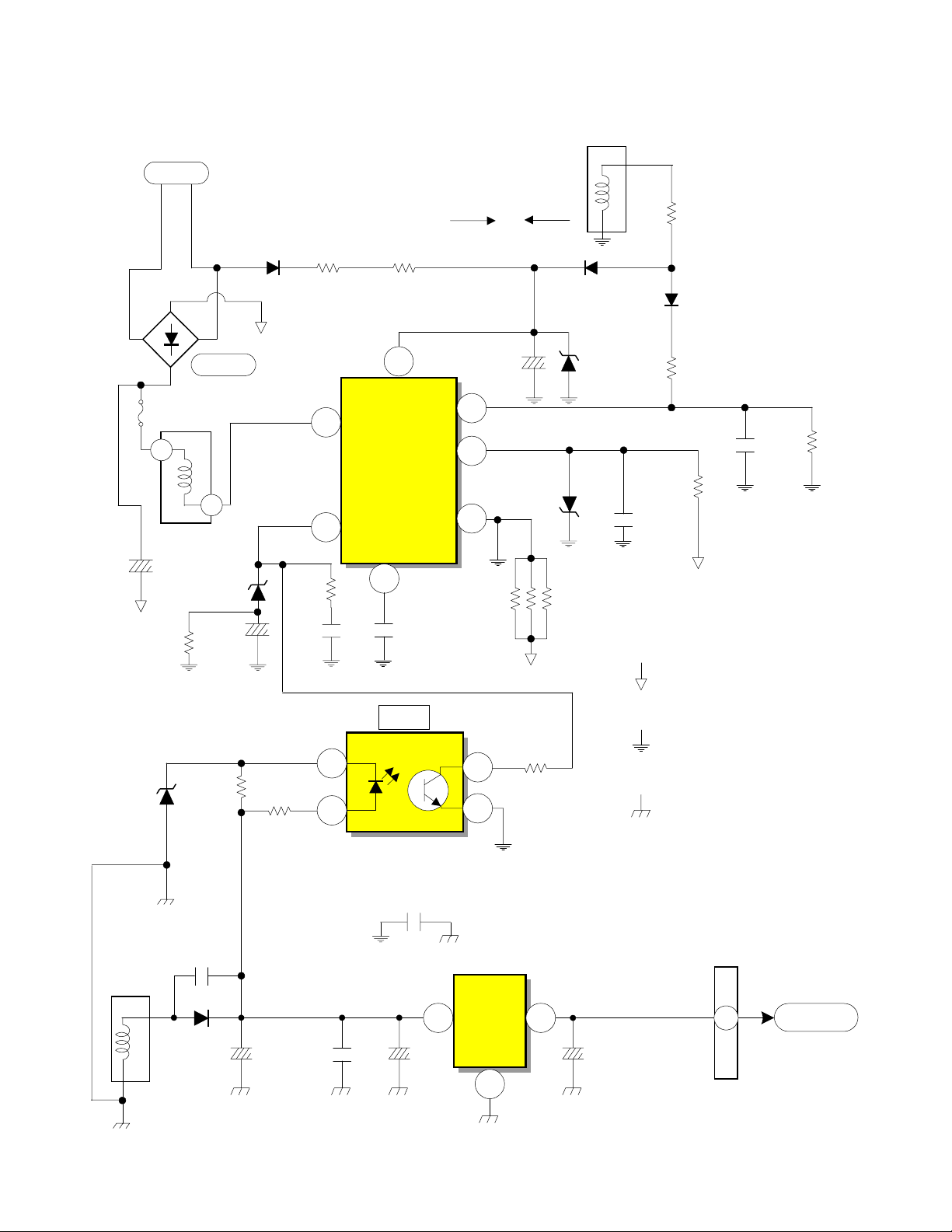
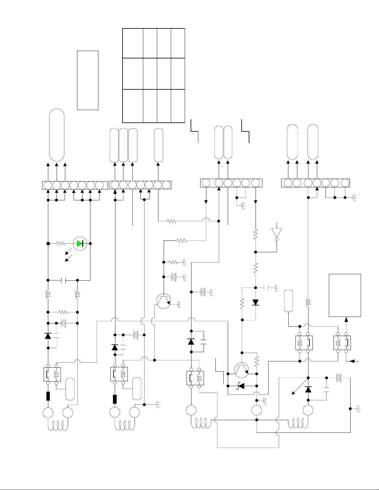
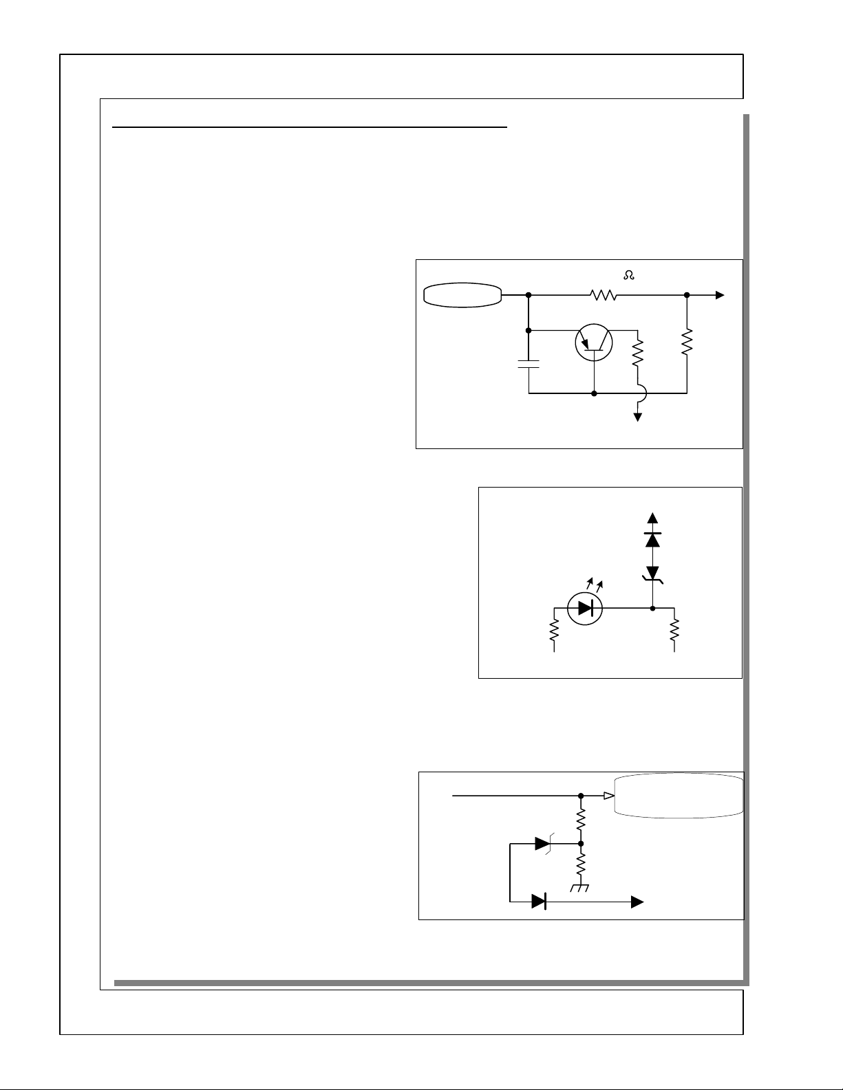
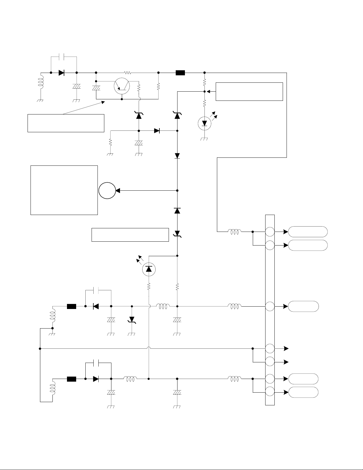
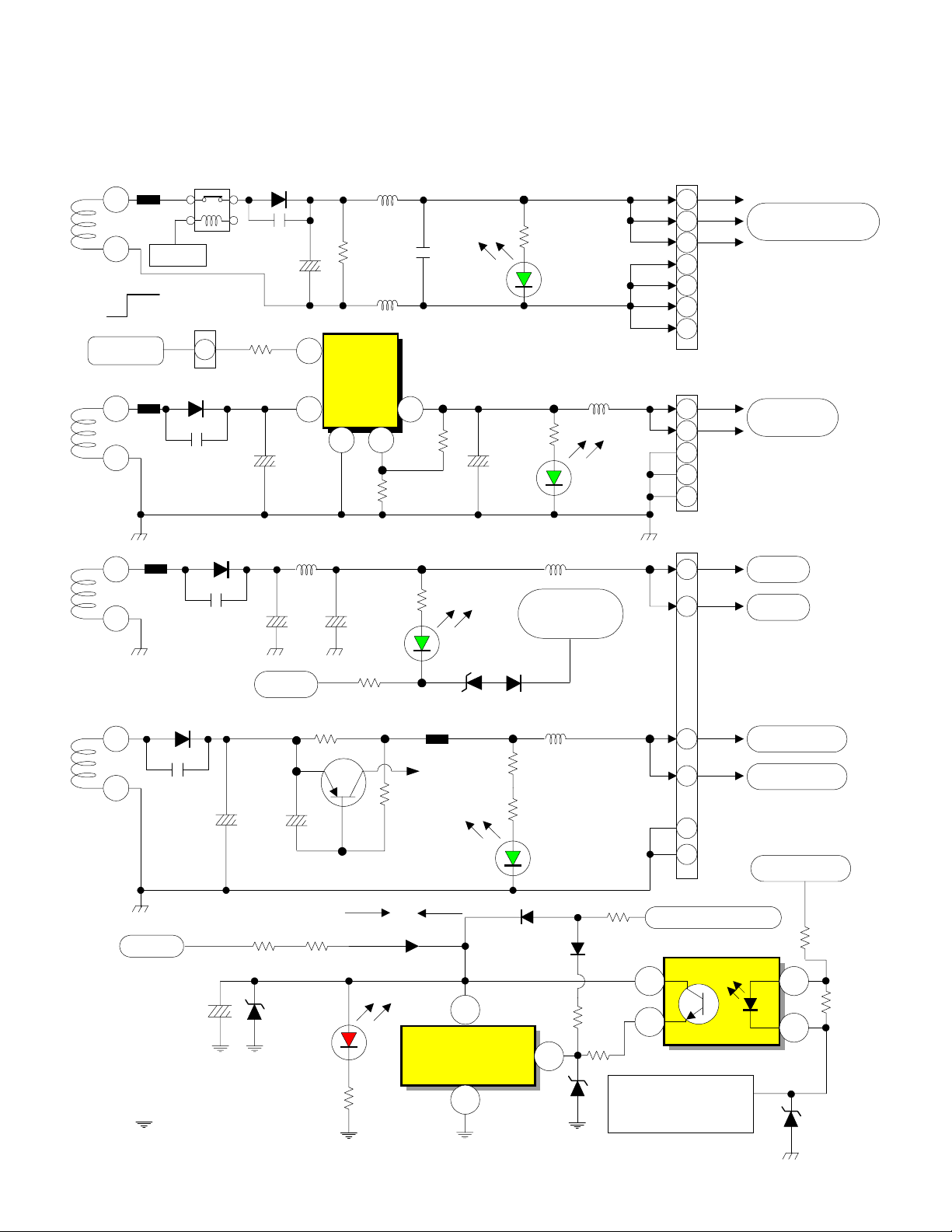
DP-2X +6V POWER SUPPLY REGULATION EXPLANATION
+6V Power Supply Circuit Diagram explanation:
(See DP-26, DP-27 and DP-27D +6V Regulation Circuit Diagram for details).
(Also, see DP-23, DP-23G and DP-24 +6V Regulation Circuit Diagram for details).
Note: Items described below for the DP-23, 23G and DP-24 are shown in brackets [ ].
THIS POWER SUPPLY RUNS ALL THE TIME:
When a Projection set is plugged into an AC outlet, it must produce a power supply to energize certain circuits.
These circuits are responsible for monitoring the Infrared input or Front control Keys as well as the Auxiliary
inputs if the Auto Link feature is active.
These power supplies are generally labeled as Always power supplies or Standby power supplies. As an example
would indicate a +6V power supply that’s always present. If the power supply has an Sby prefix, (example
A+6V
Sby +6V) this too is always present if the set is plugged into the AC outlet.
The DP-2X power supply Standby voltages are regulated by monitoring the
Sby +5V
The
by
REGULATION:
The primary route for the
However, the regulation route is to pin 1 of
the
pin 4 to pin 3 ground. This action causes pin 6 of
turn causes the frequency of the drive pulse delivered to the Gate of the internal SMOSFET (Switch Metal Oxide
Semiconductor Field Effect Transistor) to manipulate the frequency of the pulse generated on the primary of
T901
internally to pin 2 and then to floating ground pin
low ohm resistors,
SMOSFET is monitored. If this current exceeds a specific value, the voltage developed by these low ohm resistors is routed back into pin 5 which is the Over Current Protection circuit. This pin will inhibit the drive signal to
the gate of the SMOSFET. As soon as the excessive current situation is eliminated, the IC will recover and continue functioning.
B+ GENERATION FOR THE LOW VOLTAGE POWER SUPPLY DRIVER IC:
Vcc for the Driver IC is first generated by the AC input. This voltage is called Start Up Voltage.
16V
When AC is applied, AC is routed through the main fuse
to prevent any internal high frequency radiation for radiating back into the AC power line. After passing the filters it arrives at the main full wave bridge rectifier
supplied to the power supply switching transformer
However, one leg of the AC is routed to a half wave rectifier
R907
of
begins the operation of
When the power supply begins to operate by turning on and off the internal Switch MOS FET, the Raw 150V DC
routed through
Switch MOS FET is routed out of pin 2 through three low ohm resistors to hot ground. When the internal Switch
MOS FET turns on, it causes the transformer to saturate building up the magnet field. When the internal Switch
MOS FET turns off, the magnet field collapses and the EMF is coupled over to the secondary windings, as well
as the drive windings. The drive windings at pin
D905
Note too that Hot Ground is the Negative Leg of the bridge rectifier
T901.
after it is regulated by
Control +6V
and becomes a
C954
Control +6V
. Pin
DC to operate normal. However, it will begin operation at
(both a 68K ohm resistor), filtered by
as start up voltage. When this voltage reaches 6.8Vdc, the internal Regulator of
I901
, filtered by
is generated on the Secondary of
Power Supply.
+6V
Note: Items for the DP-23, 23G and DP-24 are shown in brackets [ ].
Control +6V
voltage fluctuations. The internal receiver receives this light and acts as a variable resistor from
6 [3]
of
T901
is routed to pin 1 of
T901
R908, R909
.
I901
, to
C911
in on pin 1 (Drain) and out on pin 2 which is the Source. The Source of the internal
I901
then routed clamped by
.
I909
is to pin 3 of
and
R910 [R908, R909
I904
I901
C911
The Primary Chassis Discussed is the DP-27 and DP-27D.
Control +6V
pin
T901
and output as
I909
. Internally, the LED is illuminated by degrees dependant upon
to manipulate the internal oscillator within
I901
which is the Drain of the SMOSFET. The source is connected
of
9 [6]
, clamped by a 30V Zener
8 [5]
D907
T901
] to hot ground. Here, the current drain of the internal
F901
where it is converted to Raw 150V DC voltage to be
D901
pin 2 [1].
T901
of
T901
and now becomes run voltage (
. The pulse is rectified by
10 [7]
Sby. +5V
. The floating ground is monitored by three [two]
6.8V DC
(a 6 Amp fuse), then through the Line filter
D904
produce a run voltage pulse which is rectified by
on pin 3 of
where it is rectified, routed through
and made available to pin (3)
D907
and the Floating Ground is pin
D901
which becomes the
from pin 2.
.
I901
is turned On and
I901
) for
16V
D941
I901
I901
I901
and filtered
. This in
requires
L901
R906
pin 3.
9 [6]
and
of
PAGE 01-01
Page 10
DP-26, DP-27 and DP-27D CHASSIS POWER SUPPLY Sby +6V REGULATION
Lo Voltage Power Supply
T902
AC
8
C910A
R917
D953
D901
F902
2
T901
150V
6
D908
C918
R958
D904
R957
R906
16.3V
1
D
I901
Driver/
Output IC
6
FB/OLP
ABS
R916
C917
2
1
Regulator Photocoupler
4
R907
3
C915
FB
I904
Osc B+
BD
OCP
S
Start Up
7
5
2
4
3
C911
D906
R915
Run
D905
D907
R908
R909
R910
9
0.47
Ohm
R913
D910
R911
R912
C914
Hot Ground from
negative leg of
Bridge D901
Floating Ground
from pin 9 of T901
Cold Ground Pin 11
Secondary of
T901
C916
R914
Control
T901
10
11
+6V
C969
D941
C954
1.79A
C904
I909
3 2
+5V
Reg
C985C972 C973
1
0.0685A
PPS3
2
Sby +5V
PAGE 01-02
Page 11

AC
DP-23, DP- 23G and DP-24 Chassis
+6.0 V Low Voltage Regulation
T901
5
C910A
R917
D901
F902
1
T901
150V
3
D908
C918
D904
C913
R916
C917
R906
1
6
R907
16.3V
3
Osc B+
D
I901
Driver/
Output IC
FB/OLP
ABS
4
BD
OCP
C915
Start Up
7
5
2
S
R908
R909
0.47
Ohm
FB
C911
D906
D905
D907
6
Run
R912
C914
Hot Ground from
R913
D910
R911
negative leg of
Bridge D901
C916
R914
D953
Control
T901
+6V
7
8
R958
C969
D941
C954
2
I904
1
R957
Regulator Photocoupler
C904
1.79A
3 2
R915
4
3
Cold Ground from
pin 8 of T901
I909
+5V
Reg
C972 C973
C985
1
Floating Ground
from pin 6 of T901
PPS3
0.0685A
2
Sby +5V
PAGE 01-03
Page 12
DP-2X POWER ON RELAY CONTROLS EXPLANATION
Relay Controls Circuit Diagram explanation:
(See DP-23, DP-23G, DP-24 and DP-27, DP-27D Relay Controls Circuit Diagram for details)
POWER ON:
When the Customer presses the Power On button on the Front control panel or the Remote control, the Microprocessor
and it’s collector connected to the Sty +5V line goes low. This action in turn causes the base of
and turns
5V.
This high is routed to the
(See the Lo Voltage Power Supply Shut Down Circuit for details), then the High from pin 4 is routed to the base
of
Q908
When
Q908
the base of
RELAYS ENERGIZED BY Q907 (DP-23, DP-23G, DP-24, DP-27 and DP-27D:
Note: This description refers specifically to the DP-27 and DP-27D chassis. Components identified inside brackets [ ] are for the DP-23, 23G and DP-24 chassis.
S901
This completes the path for AC to reach the High Voltage power supply bridge diode
age Regulation Circuit for details). This action starts the High Voltage power supply
circuit.
S902
This completes the path for the pulse generated from pin
and [+29V for DP-23, DP-23G and DP-24] to reach the Audio B+ rectifier diode
is generated and output from the
[+29V]
S903
This completes the path for the pulse generated from pin
which produces
and
IP53
S905
This completes the path for the pulse generated from pin
rectifier diode
Tuners pin 9.
DP-26 ONLY: RELAYS ENERGIZED BY POWER _1 and POWER _2:
(See DP-26 Relay Controls Circuit Diagram for details)
Power _1: (High when the Set is turned On.)
• When the Customer presses the Power On button on the Front control panel or the Remote control, the
• This high is routed to the
• When
output a High from pin 59. This high is routed to the base of
I001
to turn Off.
Q025
PPS3
turning it On.
turns on, it’s collector is connected to the
turning it On. When
Q907
SW+6V
(Switched +5V regulator) on the Signal PWB.
D943
Microprocessor
transistor On and it’s collector connected to the Sty +5V line goes low. This action in turn causes the
base of
line and it’s collector pulls up to 5V.
tivated, (See the Lo Voltage Power Supply Shut Down Circuit for details), then the High from pin 4 is
routed to the base of
Q025
Q907
to reach the
. Here the
I001
to go low and turns
turns on, it causes the following relays to energize.
collector is also connected to the
Q025
connector pin 4. Provided the
Q907
PPS5
PPS4
SW+35V
output a High from pin 59. This high is routed to the base of
Q907
is generated and output from the
connector pin 4. Provided the
PPS3
turning it On.
which turns this transistor On
Q026
Q025
Sby +5V
Short Detection
Sby +5V
turns on, it causes the following relays to energize.
connector pins 1, 2 and 3 and on to the Audio output circuit.
connector pins 7 and 6 and on to
to turn Off.
Q025
line. It’s emitter pulls up and supplies a high to
of
14 [11]
10 [7]
13 [10]
T901
of
T901
of
T901
collector is also connected to the
Q025
line and it’s collector pulls up to
transistor
D902
SW+115V
, (+38V for DP-26, DP-27 and DP-27D)
. Here the
D944
(Control +6V), rectified by diode
(Switched +3.3V regulator)
IP52
(+35V) to reach the Tuning Voltage B+
connector pin 8 and on to the
PPS3
Short Detection
isn’t activated,
Q903
. (See the High Volt-
for the deflection
Audio +38V
which turns this
Q026
transistor
to go low
Sby +5V
isn’t ac-
Q904
D941
(Continued on page 5)
PAGE 01-04
Page 13
DP-2X POWER ON RELAY CONTROLS EXPLANATION
RELAYS ENERGIZED BY Q907: Activated by Power _1
•
•
•
Power _2: (High when the set is turned On and/or when the Timer is On).
RELAYS ENERGIZED BY Q909
•
•
TIMER (Unattended Recording) OPERATION:
NOTE: Power _2
Tuners, Selector IC and Monitor output become active. During this time,
This way, the Selector IC, Tuners, Audio Circuit and Monitor outputs remain active.
The Table below shows the logic state of Power _1 and Power _2.
S901
This completes the path for AC to reach the High Voltage power supply bridge diode
High Voltage Regulation Circuit for details). This action start the High Voltage power supply
SW+115V
S902
This completes the path for the pulse generated from pin 14 of
tifier diode
and on to the Audio output circuit.
3
S903
This completes the path for the pulse generated from pin 10 of
D941
+3.3V regulator) and
• When the Customer presses the Power On button on the Front control panel or the Remote control, the
Microprocessor
• DM +9V REGULATOR:
• When Power _2 goes high, it's routed to pin 2 of
tor and it turns on. Input to pin 5 is the
to the Digital Module (ATSC Tuner) pin 12 PMS1.
3
• The DM +9V is also routed to the Terminal PWB pin 21of the
tor IC
• Power _2 is also routed to the
to the base of
• When
S905
This completes the path for the pulse generated from pin 13 of
age B+ rectifier diode
and on to the Tuners pin 9. This voltage is also routed out the PPS7 connector pin 6
come tuning voltage for the Digital Tuner (ATSC) via pin 1 of the
S906
This completes the path for the pulse generated from pin
rectifier diode
and on to the DM +9V regulator
from pin 3 to the Digital Module (ATSC Tuner) pin
for the deflection circuit.
, (+38V) to reach the Audio B+ rec-
T901
. Here the
D944
which produces
I001
and the Monitor Out Circuit.
IX01
Q909
turns on, it causes the following relays to energize.
Q909
D945
is also high when the Timer is set for unattended recordings. When the Timer is activated, the
Audio +38V
SW+6V
IP53
output a High from pin 58. This high is routed to two different circuits.
turning it On.
D943
. Here the
to reach the
(Switched +5V regulator) on the Signal PWB.
PPS3
: Activated by Power _2
. Here the
DM +10V
is generated and output from the
(Control +6V), rectified by diode
T901
connector pins 7 and 6 and on to
PPS4
on the Signal PWB. This is the
IP01
DM +10V, IP01
connector pin 4 and then to the Power Supply. This high is routed
SW+35V
. Input to pin 5,
IP01
is generated and output from the
is generated and output from the
regulates this down to 9V and output it from pin
connector. This turns on the Selec-
PST2
(+35V) to reach the Tuning Volt-
T901
PMS2
Digital Module +10V) of
17 (
regulates this down to
IP01
12
of the
PMS1
connector.
Power_1
connector pins 1, 2 and
PPS5
IP52
PPS3
connector.
connector pin 2 and 3
PPS7
+9V
remains Low.
. (See the
D902
(Switched
DM +9V
connector pin 8
DM +28V
T901
and outputs it
regula-
, to be-
to reach the
MODE POWER _1 POWER _2
Stand By L L
Timer L H
Power ON H H
PAGE 01-05
Page 14
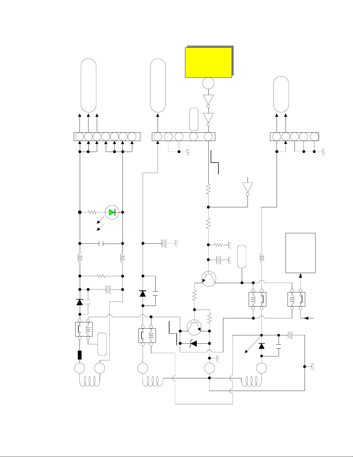
I001
59
Micro
Audio + 29V
Audio Gnd
Audio Gnd
Audio Gnd
Audio Gnd
1
2
3
4
5
6
7
PPS5
1.30A
D965
R985
GREEN L.E.D.
C978
L922
L921
R992
Sby 5V comes from I909 pin 2
SW + 35V
8
PPS3
0.0165A
Gnd
3
C956
Gnd
7
Sby +5V
4
2
POWER _1
R962 R963
Q908
Q025 Q026
On
R961
C957
Off
SW + 6V
Gnd
Gnd
6
7
5
Gnd
4
3
PPS4
Short Det.
See Power Supply Shut Down Circuit
1.33A
Q903
Sby +5V
L923
AC to D902
High Voltage
Power Supply
D943
C962
D944
C957
DP-23, DP-23G and DP-24 Chassis Power On Relay Controls
C961
R960
R959
Q907
Off
Supply Relay
S-902 Audio Power
E911
11
+29V
T901
Sby +5V
12
Supply Relay
S-905 SW +35V
10
+35V
On
D954
8
T901
Supply Relay
S-903 SW +6V
Control +6V
S-901 Main
Power Relay
AC
D941
C959
C954
7
PAGE 01-06
Page 15
Sby 5V comes
from I909 pin 3
_2
POWER
_1
POWER
MODE
L
H
L
L
Timer
Stand By
H
H
TV On
From Micro Pin 58
From I909
On
From Micro Pin 59
From I911
On
Audio + 38V
Audio Gnd
Audio Gnd
Audio Gnd
Audio Gnd
1
2
3
4
5
6
7
PPS5
1.55A
R985
D965
GREEN L.E.D.
DP-26 RELAY CONTROLS
L922
C978
L921
R992
DM +10V
2
1.55 A
DM +10V
Sby +10V
1
3
0.36 A
From D942
DM +28V
Audio Gnd
Audio Gnd
4
5
6
0.006 A
Q909
N/C
7
PPS7
R973
R963
C968
R984
Off
POWER _2
5
PPS3
C956
SW + 35V
1
1.30A
0.25 A
SBY + 5V
Gnd
3
2
R960
POWER _1
Gnd
7
4
R962 R963
Off
PPS4
Q904
C957
D972
SW + 9V
1
SW + 6V
6
7
2
1.06A
1.54A
Short Det.
Shut Down Circuit
See Power Supply
Sby +5V
L923
Gnd
5
Gnd
Gnd
4
3
AC to D902
High Voltage
Power Supply
D944
S-902
SW +35V Relay
E911
14
+38V
Audio
C952
T901
C957
Sby +5V
15
D945
S-906 Digital
Module 10 V Relay
E912
17
C963
16
T901
C958
Sby +5V
D943
Supply Relay
S-905 SW +35V
13
+35V
C961
Off
On
Q907
D954
T901
R959
11
Supply Relay
S-903 SW +6V
Control +6V
10
S-901 Main
Power Relay
D941
C954
C959
PAGE 01-07
AC
Page 16

I001
59
Micro
Audio + 38V
Audio Gnd
Audio Gnd
Audio Gnd
Audio Gnd
1
2
3
4
5
6
7
PPS5
1.95A
D965
R985
GREEN L.E.D.
C978
L922
L921
R992
Sby 5V comes from I909 pin 3
SW + 35V
8
PPS3
0.0165A
Gnd
3
C956
Gnd
7
Sby +5V
4
2
POWER _1
R962 R963
Q908
Q025 Q026
On
R961
C957
Off
SW + 6V
Gnd
Gnd
6
7
5
Gnd
4
3
PPS4
Short Det.
See Power Supply Shut Down Circuit
1.33A
Q903
Sby +5V
L923
AC to D902
High Voltage
Power Supply
C961
R960
R959
Supply Relay
S-903 SW +6V
D944
C962
C957
D943
Q907
Off
DP-27 and DP-27D CHASSIS RELAY CONTROLS on the POWER SUPPLY
Supply Relay
S-902 Audio Power
E911
14
+38V
T901
Sby +5V
15
Supply Relay
S-905 SW +35V
13
+35V
On
D954
11
Control +6V
10
D941
S-901 Main
Power Relay
C959
AC
C954
PAGE 01-08
Page 17

DP-2X LOW VOLTAGE POWER SHUT DOWN EXPLANATION
Low Voltage Power Supply Shut Down Circuit Diagram explanation:
(See DP-27 Signal Power Supply (Low Voltage) Shut-Down Circuit Diagram for details)
The Low Voltage power supply is centered around the Switching Transformer
This power supply creates the Standby voltages
let. It also creates other voltages that are Switched on when the Set is turned on.
Audio +38V
SW +35V
SW +9V
SW +HVcc
The following explanation will describe the Low Voltage Power Supply Shut Down Circuit.
POWER SUPPLY SHUTDOWN PHOTO COUPLER I905 EXPLANATION
This chassis utilizes I901 as the Osc.\Driver \Switch for the Low Voltage power supply, just as the previous chassis have done. The Shutdown circuit, (cold ground side detection), removes
circuit,
signal to the Hot Ground side,
it removes B+ from pin (3) of
The Power Supply utilizes a Shutdown circuit that can trigger
tection circuits are not operational in Stand By mode).
forward biases the internal LED. The light from this internal LED is then coupled to the receiver transistor. The
receiver transistor turns On and output a High from pin 3. This high is routed to the base of
which grounds out the Vin at pin (3) of
Q902
The individual Shut Down circuits will be discussed later.
GENERAL INFORMATION:
All of the Power Supply Shutdown circuitry can be broken down into the following category;
•
•
•
•
The following will explain all of these commonly used circuits. The Service Technician should become familiar
with the appearance of these circuit and their function.
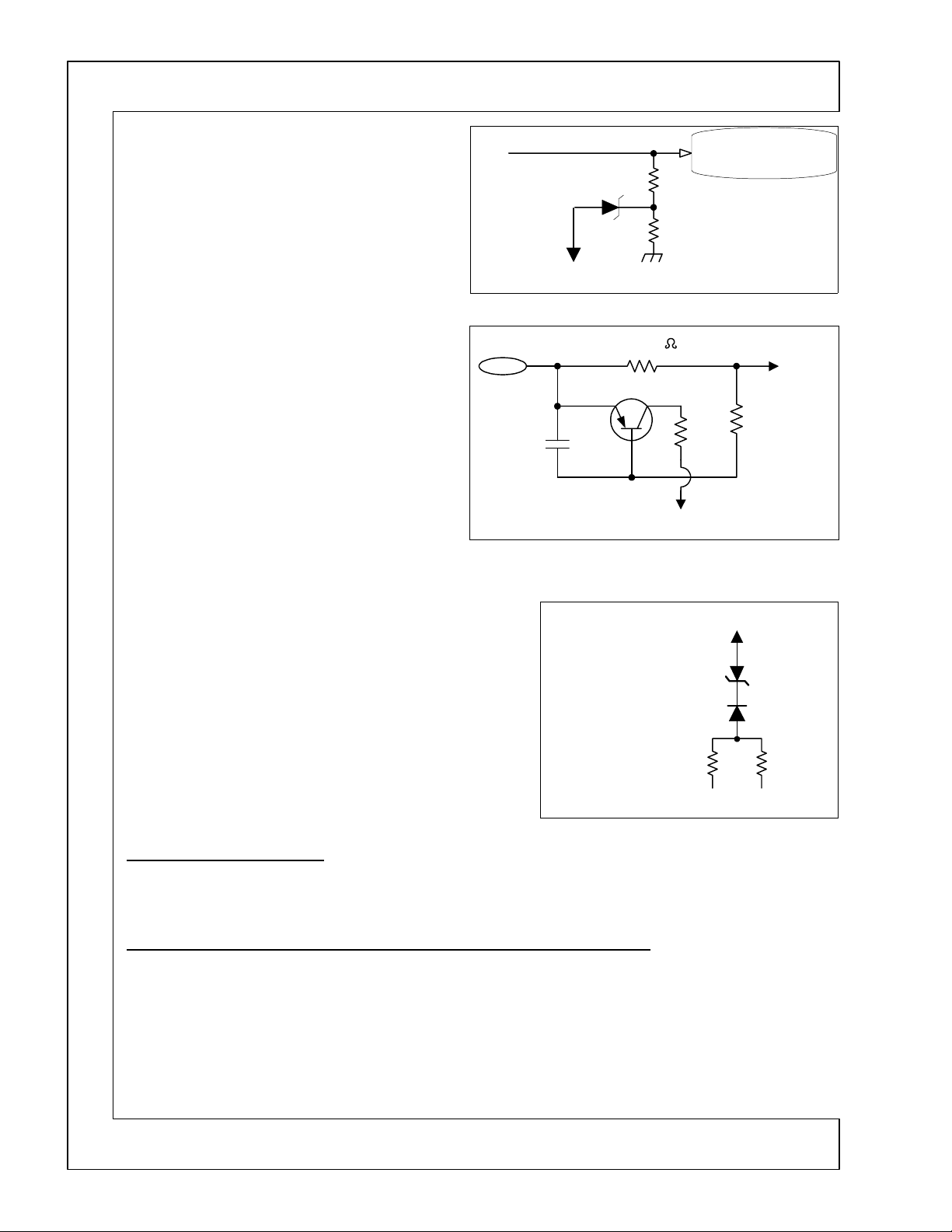
VOLTAGE LOSS or SHORT DETECTION
(See Figure 1)
One circuit used is the
cuit. This is a very simple circuit that detects a loss of
a particular power supply and supplies a Pull-Down
path for the base of a PNP transistor.
This circuit consist of a diode connected by its cathode to a positive B+ power supply. Under normal
conditions, the diode is reversed biases, which keeps
the base of Q1 pulled up, forcing it OFF. However, if
there is a short or excessive load on the B+ line that’s
being monitored, the diode in effect will have a LOW
on its cathode, turning it ON. This will allow a current path for the base bias of Q1, which will turn it
ON and generates a Shutdown Signal.
(the Photo Coupler), which isolates the Hot ground from the Cold ground and couples the Shutdown
I905
on the hot ground side and
Q902
(the Vin pin).
I901
I901
as long as there is any voltage available at its Emitter.
Voltage Missing Detection or Short Detection
Voltage Too High Detection
Excessive Current Detection
Negative Voltage Loss Detection
Voltage Loss Detection
SBY +5V
, disabling the power supply.
cir-
which runs anytime the set is plugged into an AC out-
Q901
Q902
is activated by a Low being applied to pin 2, which
I905
Voltage
Loss
Detector
Figure 1
and
T901
B+ at pin 3 via the following
I901
which latches
from 2 input sources. (1 of these Short De-
Q901
Q902
will keep a high on the base of
I901.
on. When
turning it On,
Q902
Any Positive
B+ Supply
Q902
B+
is on,
Q1
Shut-Down Signal
(Continued on page 10)
PAGE 01-09
Page 18
DP-2X LOW VOLTAGE POWER SHUT DOWN EXPLANATION
VOLTAGE TOO HIGH DETECTION
(See Figure 2)
Another circuit used is the
circuit. In the example shown in Figure 2, the
tion
zener diode
the voltage source rises too high, the voltage at the
divider center point will rise as well and trigger or fire
the zener diode which produces a Shutdown signal.
EXCESSIVE CURRENT DETECTION
(See Figure 3)
One very common circuit used in many Hitachi television products is the B+
circuit. In this circuit is a low ohm resistor in series
with the particular power supply, (labeled B+ in the
drawing). The value of this resistor is determined by
the maximum current allowable within a particular
power supply. In the case of Figure 1, the value is
shown as a
ohm value. When the current demand increases, the
voltage drop across the resistor increases. If the voltage drop is sufficient to reduce the voltage on the base
of the transistor, the transistor will conduct, producing
a Shutdown signal that is directed to the appropriate
circuit.
NEGATIVE VOLTAGE LOSS DETECTION
(See Figure 4)
The purpose of the Negative Voltage Loss detection circuit is to
compare the negative voltage with its’ counter part positive voltage. If at any time, the negative voltage drops or disappears, the
circuit will produce a Shutdown signal.
In Figure 5, there are two resistors of equal value. One to the
positive voltage, (shown here as +12V) and one to the negative
voltage, (shown here as -12V). At their tie point, (neutral point),
the voltage is effectually zero (0) volts. If however, the negative
voltage is lost due to an excessive load or defective negative
voltage regulator, the neutral point will go positive. This in turn
will cause the zener diode to fire, creating a Shutdown Signal.
SPECIFIC INFORMATION:
In addition, there are 7 Hot Ground side Shutdown inputs that are specifically detected by the main power driver
IC
HOT GROUND SIDE SHUT DOWN SENSING CIRCUITS. (Specific to I901).
LATCHED SHUT DOWN MONITORS:
1. (OVP)
2. (TSD)
3. (OLP) Over Load Protection monitors the difference between the Hot Ground and Floating Ground.
RECOVERING SHUT DOWN INPUT:
4. (OCP)
. These sensors circuits protect
I901
is connected to a voltage divider. If
D1
0.47 ohm
is monitored for Over Voltage Protection at pin 3 of
Pin 3
itself is monitored for Excessive Heat. This block is labeled TSD. (Thermal Sensing Device).
I901
monitors the low ohm resistors,
Pin 5
Voltage Too High Detec-
Excessive Current Sensing
, however it could be any low
Voltage Too High
Detector
Shut-Down Signal
B+
Current Sensor
Figure 3
R1
0.47
Shut-Down Signal
Shut-Down Signal
Any Positive
Voltage
Loss
Detector
from excessive current, temperature or over voltage.
I901
(AC must be removed to recover).
(Driver IC will recover on it’s own when trouble is removed.)
R908, R909,
and
Figure 4
.
I901
. If these resistors have an excessive
R910
+12V -12V
(Continued on page 11)
B+ Supply
Figure 2
Base
Bias
PAGE 01-10
Page 19

DP-2X LOW VOLTAGE POWER SHUT DOWN EXPLANATION
current condition caused by monitoring the current through the internal Switch MOS FET, the voltage will
rise and pin 5 has an internal Over Voltage detection op-amp. If this voltage rises enough to trigger this opamp, the IC will stop producing a drive signal.
5. (ABS)
of High Voltage.
6. (BD)
COLD GROUND SIDE SHUT DOWN SENSING CIRCUITS.
(See DP-27 Signal Power Supply (Low Voltage) Shut-Down Circuit Diagram for details)
Looking at Pin 2 of
D963, D962:
The cathode of
connected directly to the
this line down,
a Shut Down event. See Power Supply Shutdown Photo Coupler I905 Explanation on the previous page.
Q910:
This transistor’s base is connected to
the Shut down enable circuit.
DP-27 SHUT DOWN CIRCUIT:
There are a total of 3 individual Shutdown inputs to the photo coupler
There are a total of 3 individual Shutdown inputs to the Relay Inhibit transistor
There are a total of 4 individual Shutdown inputs to the Relay Inhibit transistor
cuit. For a total of 10 individual Shutdown inputs that will kill the Lo Voltage Power Supply. (Note: The Hi Volt-
age Power Supply Shutdown will be discussed later.)
All of the Cold Ground side Shutdown detection circuits can be categorized by the two previously described circuits
In the following explanation, the Shutdown circuits will be grouped. This will assist the Service Technician with
trouble shooting the Chassis, by understanding these circuits and having the associated circuit routs, the technician can then “Divide and Conquer”.
Voltage Loss Detection through I905 Photo coupler
• Shorted STBY +3.3V generated by
to (
• Shorted SW+2.2V (
on Low Voltage Power Supply PWB. Labeled
• Shorted SW+3.3V (
(
• Shorted SW+5V (
(
Q903 Relay Inhibit Activation.
From the Power Supply.
SW +115V Voltage Too High Detection
• Monitored by (
SW +115V Excessive Current Detection
• Monitored by (
also has
Pin 4
Monitors the Run Voltage generated by pin 18 of
Pin 7
I905
is connected through
D963
would forward bias and supply a current path for pin 2 of
D963
) on Low Voltage Power Supply PWB. Labeled
D963
) on Low Voltage Power Supply PWB. Labeled
D961
) on Low Voltage Power Supply PWB. Labeled
D961
D927
Q905
monitoring spike current in case the CRTs “Snap” indicating a quick discharge
C915
the shut down events are triggered by two routes.
to pin 10 of
R982
power supply produced by
3.3V
through
Q911
pin 5) on Signal PWB monitored by
IP52
pin 2) on Signal PWB monitored by
IP52
pin 2) on Signal PWB monitored by
IP53
) See additional Shut Down Circuit Diagram for details.
) See additional Shut Down Circuit Diagram for details
D955. Q911
and monitored by (
IP81
IP81
PROT-SW
for excessive voltage.
T901
(AC must be removed to recover).
. This in turn is connected to
PPS3
on the Signal PWB. If something were to load
This in turn would produce
I905.
emitter is connected to
.
I905
Q903
Q903
) on Signal PWB through
R298
PROT-SBY
RP53
on the Schematic.
DP53, RP53
PROT-SW
DP54, RP53
PROT-SW
on the Schematic.
through
on the Schematic.
on the Schematic.
Q912
from the power supply.
from the Deflection Cir-
pin 11 to to (
PPS3
through
through
PPS3
PPS3
which is
R298
. This transistor is
pin 10
PPS3
D961
pin 11 to to
pin 11 to to
(Continued on page 12)
)
PAGE 01-11
Page 20

DP-2X LOW VOLTAGE POWER SHUT DOWN EXPLANATION
SW –28V Loss Detection
• Monitored by (
From the Deflection Circuit PPD3 connector pin 6.
Vertical B+ 28V Voltage Excessive Current Detection
• Monitored by (
Excessive High Voltage Detection
• Monitored by (
-5V Loss Detection
• Monitored by (
Side Pincushion Failure Detection
• Monitored by (
If any one of these circuits activate the base of
connector pin 4 and the power supply will STOP.
SOME SHUTDOWN CIRCUITS ARE DEFEATED IN STANDBY MODE. (Set Off).
As indicated in the Power Supply (Lo Voltage) Shutdown circuit diagram, 3 of the shut down inputs are not active when the set is in standby.
• Shorted SW+2.2V (
on Low Voltage Power Supply PWB. Labeled
• Shorted SW+3.3V (
(
) on Low Voltage Power Supply PWB. Labeled
D961
• Shorted SW+5V (
(
) on Low Voltage Power Supply PWB. Labeled
D961
These voltage loss sensing circuits are defeated because the SW (Switched) power supplies are turned off in
standby. So to prevent faults triggering of the shutdown circuit, the sensing circuits are turned off also..
supplies the high for shutdown if any of the voltage loss circuits become activated.
Q911
voltage to operated. Emitter voltage is supplied from the emitter of
on/off line. When the set is not on or turned off, the power on/off line goes Low. This Low pulls the cathode of
low, removing the base voltage of
D956
this circuit can not function. The base of
for this circuit to function.
B+ GENERATION FOR THE LOW VOLTAGE POWER SUPPLY DRIVER IC:
Vcc for the Driver IC is first generated by the AC input. This voltage is called Start Up Voltage.
DC to operate normal. However, it will begin operation at
16V
When AC is applied, AC is routed through the main fuse
to prevent any internal high frequency radiation for radiating back into the AC power line. After passing the filters it arrives at the main full wave bridge rectifier
supplied to the power supply switching transformer
However, one leg of the AC is routed to a half wave rectifier
(both a 68K ohm resistor), filtered by
R907
of
as start up voltage. When this voltage reaches 6.8Vdc, the internal Regulator of
I901
begins the operation of
When the power supply begins to operate by turning on and off the internal Switch MOS FET, the Raw 150V DC
routed through
MOS FET is routed out of pin (2) through three low ohm resistors to hot ground. When the internal Switch MOS
FET turns on, it causes the transformer to saturate building up the magnet field. When the internal Switch MOS
FET turns off, the magnet field collapses and the EMF is coupled over to the secondary windings, as well as the
drive windings. The drive windings at pin (8) produce a run voltage pulse which is rectified by
then routed clamped by
C911
T901
) See additional Shut Down Circuit Diagram for details
D937
) See Deflection Protect Power Supply Shutdown Diagram for details.
Q604
) See Deflection Protect Power Supply Shutdown Diagram for details.
DH15
) See Deflection Protect Power Supply Shutdown Diagram for details.
DK90
D702, D703
IP53
.
I901
, in on pin 1 (Drain) and out on pin 2 which is the Source. The Source of the internal Switch
) See Deflection Protect Power Supply Shutdown Diagram for details
will go High and remove the Power On High from
Q903
pin 5) on Signal PWB monitored by
IP52
PROT-SW
pin 2) on Signal PWB monitored by
IP52
pin 2) on Signal PWB monitored by
turning it OFF. This removes the emitter voltage from
Q912
is also connected to the
Q912
F901
where it is converted to Raw 150V DC voltage to be
D901
pin (2).
T901
D904
, clamped by a 30V Zener
C911
and now becomes run voltage (
D907
on the Schematic.
PROT-SW
DP54, RP53
PROT-SW
Q912. Q912s
6.8V DC
(a 6 Amp fuse), then through the Line filter
where it is rectified, routed through
16V
through
RP53
DP53, RP53
on the Schematic.
on the Schematic.
SW +6V
on pin (3) of
D907
) for
through
through
base is connected to the power
line. This voltage must be active
and made available to pin (3)
pin 3.
I901
PPS3
Q911
I901
I901
PPS3
pin 11 to to (
PPS3
pin 11 to to
PPS3
requires emitter
I901
.
is turned On and
D905
D961
pin 11 to to
Q911
requires
R906
, filtered by
)
and
L901
and
PAGE 01-12
Page 21
DP-2X SIGNAL POWER SUPPLY (Low Voltage) SHUT-DOWN CIRCUIT
D904
R906
R907
16.97V
T901
D905
D941
8
10
Control +6V
C911
AC
Monitors
SW +5V
SW +3.3V
SW +2.5V
and
Stby +3.3V
for Short
To R298
Monitors IP81
To RP53
Monitors IP52
and IP53
Sby +5V
S901
Relay
AC
To Hi Volt
Power
Supply
D954
HZS11B1
Protect _Def
4 from Deflection
See Deflection Shut
Down Circuits
Q907
16.3V
Q901
S-905
SW +35V
Supply
Relay
R960
R959
6
PPD3
Vin
3
I901
Power IC
Q902
C920
R921
Protect _Sby
3.3V Reg
Protect _Sw
+5V Reg
SW +35V
Q908
C957
Q904
D933
R940
C944
R919
C919
47 Ohm
R920
PPS3
10
11
R980
8
D946
See Relay Control
Diagram for all
Relay Controls
R962
R962
1K
C987
Q903
R938
D907
R922
D962
HZS3C1
D963
R982
D960D961
D957
4
R963
220
R939
10K
R913
I905
HZS4A1
C956
9
11
R956
1
23
Q910
C969
Q911
R967
R966
C970
SW +35V
R969
D956
C971
PPS3
Power _1
4
Off
On
See additional
Power Supply Shut
Down Circuits
A
C955
D952
D955
Q912
+6V
S-903 SW +6V
Supply Relay
2
R964
R965
SW +6V
R968
I909
Sby +5V
PAGE 01-13
Page 22

DP-2X SW +115V POWER SUPPLY REGULATION EXPLANATION
Hi-Voltage Power Supply Circuit Diagram explanation:
(See DP-27 Chassis Power Supply SW+115V Regulation Circuit Diagram for details)
THIS POWER SUPPLY RUNS ONLY WHEN THE SET IS TURNED ON:
TURNING ON THE SW +115V POWER SUPPLY:
When the Set is turned on, the Microprocessor
command is routed through
provided the Short Detection Shut Down sensor
Q908
it’s emitter will go high and drive the base of
power on Relay
See Relay Controls on the Power Supply for details.
This rectifier develops raw 150V which is routed through
through the primary coil inside
Switch MOS FET. The Ground return path for the primary voltage is out pin 2 of
internal Switch MOS FET and then through three low ohm resistors
Regulation Circuit Diagram for details.
SW +115 REGULATION
SW +115V pulse is generated from pin 11 of
routed through the Excessive Current sensing circuit
The primary route for the
to the Deflection Circuit.
However, the regulation route is through
variable resistor whose resistance is dependant upon the
resistor manipulates the current flow from pin 2 to pin 3 ground. This will cause the voltage at pin 2 of
manipulated. Internally, the LED is illuminated by degrees dependant upon the
The internal receiver receives this light and acts as a variable resistor from pin 4 to pin 3 which is the regulation
control signal.
This action causes pin 1 of
quency of the drive pulse delivered to the Gate of the internal SMOSFET (Switch Metal Oxide Semiconductor
Field Effect Transistor) to manipulate the frequency of the pulse generated on the primary of
drain of the internal SMOSFET is monitored by the three low ohm resistors mentioned above. If this current exceeds a specific value, the voltage developed by these low ohm resistors is routed back into pin 1 which is the
Over Current Protection circuit as well as the Regulation Control pin. This pin will inhibit the drive signal to the
gate of the SMOSFET. As soon as the excessive current situation is eliminated, the IC will recover and continue
functioning.
B+ GENERATION FOR THE HIGH VOLTAGE POWER SUPPLY DRIVER IC:
Vcc for the Driver IC is first generated by the AC input. This voltage is called Start Up Voltage.
DC to operate normal. However, it will begin operation at
16V
When AC is applied to the main full wave bridge rectifier
to be supplied to the power supply switching transformer
However, one leg of the AC is routed to a half wave rectifier consisting of
sistor), filtered by
When this voltage reaches 6.8Vdc, the internal Regulator of
When the power supply begins to operate by turning on and off the internal Switch MOS FET, the Raw 150V DC
routed through
MOS FET is routed out of pin (2) through three low ohm resistors to hot ground. When the internal Switch MOS
FET turns on, it causes the transformer to saturate building up the magnet field. When the internal Switch MOS
FET turns off, the magnet field collapses and the EMF is coupled over to the secondary windings, as well as the
drive windings. The drive windings at pin (8) produce a run voltage pulse which is rectified by
then routed clamped by
C923
The RED LED
turning it on. When the relay is energized, AC is supplied to the Bridge rectifier
S901
SW +115V
, clamped by a 36V Zener
C923
, in on pin 1 (Drain) and out on pin 2 which is the Source. The Source of the internal Switch
T902
can be used to determine if the B+ to I902 is present or not.
D915
and
Q025
and out pins 5 and 6 to pin 3 of
T902
to manipulate the internal oscillator within
I902
and now becomes run voltage (
D912
to the
Q026
is through
E906
Outputs a Power On command via pin 59. This Power On
I001
PPS3
high turning it on. This will supply a ground path for the
Q907
. This pulse is rectified by
T902
E907, L914
to pin 1 of
D912
connector pin 4. This High will be passed to the base of
isn’t activated. When the base of
Q903
to Pins 1 and 2 of
F903
which is the Drain of the internal
I902
R926, R927
D915
and
R941
to pin 9 and 10 of
I907
SW +115V
D902
T902
and made available to pin 4 of
I902
.
Q905
. Internally, the regulator transistor works as a
voltage fluctuations. The internal variable
I902
6.8V DC
where it is converted to Raw 150V DC voltage
pin 1 and 2.
on pin 4 of
R924
is turned On and begins the operation of
) for
16V
I902
. This voltage is routed
T902
which is the Source of the
I902
and
, filtered by
PPD6
SW +115V
. This in turn causes the fre-
and
pin 4.
. See SW+115V
R928
and output as
voltage fluctuations.
.
I902
(both a 3.9K ohm re-
R925
as start up voltage.
I902
Q908
C927
. The current
T902
I902
D911
goes high,
D902
and then
SW +115V
I906
requires
, filtered by
.
to be
I902
.
PAGE 01-14
Page 23
T902
DP-2X CHASSIS POWER SUPPLY SW +115V REGULATION
High Voltage Power Supply
8
7.5P/P
9
AC
From Relay S901
C923
AC for D902
Supplied from
Relay S901
From Bridge D902
150V
1
F903
2
D912
T902
D915
RED L.E.D.
R934
R924
16.3V
4
I902
Driver/
Output IC
3 2
DS
6
R925
OCP
Start Up
Osc B+
1
R929
R926
R927
R928
0.22
Ohm
Run
D911
R930
D914
R931
R932
C926
D913
I907
1 2
4
3
Regulator Photocoupler
I906
Hot Ground from
pin 9 of T902
R936
SW + 115V
R937FB
1
R935
2
D922
T902
11
12
C933
D915
C927
C945
X-Ray
Protect
5
6
Q905
R941
0.47 Ohm
D924
D925
D926
R943
R942
D927
E906
0.5K
3K
E907
R945
R946
L914
Deflection
B+ 115V
D928
C942
3
PPD6
0.69A
9
10
Cold Ground from
pin 12 of T902
C905
C941
SW +115V
SW +115V
PAGE 01-15
Page 24
DP-2X ADDITIONAL SHUTDOWN CIRCUITS EXPLANATION
Additional Power Supply Shut Down Circuit Diagram explanation:
(See DP-27 Additional Power Supply Shut Down Diagram for details)
Use this explanation and Diagram in conjunction with the following diagrams.
DP-2X Signal Power Supply (Low Voltage) Shut Down Circuit (Continuation A)
The following circuits are routed to the Lo Voltage Shut Down Circuit through connection point (A) depicted on the Circuit drawing:
SW +115V EXCESSIVE CURRENT DETECTION
(See Figure 1)
One very common circuit used in many Hitachi television products is the B+
circuit. In this circuit is a low ohm resistor in series
with the SW +115V. The value of this resistor
. When the current demand increases, the voltage
ohm
drop across the resistor increases. If the voltage drop
is sufficient to reduce the voltage on the base of
, the transistor will conduct, producing a Shut-
Q905
down signal that is directed to the appropriate circuit
indicated on the drawing as point
NEGATIVE VOLTAGE LOSS DETECTION
(See Figure 2)
The purpose of the Negative Voltage Loss detection circuit is to
compare the negative voltage with its’ counter part positive voltage. If at any time, the negative voltage drops or disappears, the
circuit will produce a Shutdown signal.
In Figure 2, there are two resistors of equal value, (15K). One to
the positive voltage SW +28V and one to the negative voltage
SW –28V. At their tie point, (neutral point), the voltage is effec-
tually zero (0) volts. If however, the negative voltage is lost, the
neutral point will go positive. This in turn will cause the zener
diode D937 to fire, creating a Shutdown Signal through
and on to the appropriate circuit indicated on the drawing as
point
Note: The LED
supply.
VOLTAGE TOO HIGH DETECTION
(See Figure 3)
Another circuit used is the
tion
zener diode
the voltage source rises too high, the voltage at the
divider center point will rise as well and trigger or fire
the zener diode which produces a Shutdown signal
through
cated on the drawing as point
.
(A)
D940
circuit. In the example shown in Figure 3, the
D927
and on to the appropriate circuit indi-
D926
Excessive Current Sensing
0.47
.
(A)
used for visual trouble shooting is illuminated by the current draw from +28V to the –28V
Voltage Too High Detec-
is connected to a voltage divider. If
.
(A)
SW +115V
D936
Figure 3
Figure 1
Figure 2
SW +28V
D927
D926
0.47
R941
Current Sensor
Q905
Shut-Down Signal
Shut-Down Signal
Voltage
Loss
Detector
D940
Voltage Too
High Detector
Base
Bias
D936
D937
SW -28V
SW +115V
Shut-Down
Signal
PAGE 01-16
Page 25
T902
DP-2X ADDITIONAL POWER SUPPLY SHUT DOWN DIAGRAM
C933
3K
E907
Deflection B+ 115V
D915
Q905
R941
0.47 Ohm
11
C927
12
Deflection B+ (115V)
Excessive Current Det.
See Signal Power Supply
(Lo Voltage)
Shut Down Circuit
Diagram
for continuation.
C945
R943
D924
R944
C946
D925
A
SW-28V Short or Loss Det.
R942
D927
D926
R945
R946
D936
D937
Deflection B+ (115V)
Excessive Voltage Det.
D928
Deflection B+ 115V
PPD6
L914
0.69A
9
10
SW +115V
SW +115V
T902
T902
15
13
14
10K
E901
10K
E902
C934
D917
C928
C935
D918
C929
-
+
+
-
D940
R952
D971
L913
L912
C950
C949
R951
-
+
+
-
L915
L916
0.575A
1.09A
5
3
4
1
2
SW -28V
Gnd
Gnd
SW +28V
SW +28V
PAGE 01-17
Page 26

DP-2X PROTECT SHUTDOWN CIRCUIT EXPLANATION
0.68
DK90
.
SW +28V
Figure 1
through
.
D703
PPD3
and
DH15
R629
Current Sensor
Q604
through
pin 6.
DH13
.
DH14
to stop producing the Hi
IH01
0.68
Shut-Down Signal
pin 6. This signal is
PPD3
Shut-Down Signal
DK90
+5V -5V
and
Base
Bias
Voltage
Loss
Detector
Protect Shut Down Circuit Diagram explanation:
(See DP-27 Protect Shut Down Diagram for details)
Use this explanation and Diagram in conjunction with the following diagram,
DP-2X Signal Power Supply (Low Voltage) Shut Down Circuit (PROTECT _DEF)
The following circuits are routed to the Lo Voltage Shut Down Circuit through connection point
(PROTECT _DEF) depicted on the Circuit drawing:
EXCESSIVE HIGH VOLTAGE DETECTION
Whenever the High Voltage fluctuates, every other pin off the flyback will fluctuate as well. In this case, a lower
voltage source can be used to determine the status of the High Voltage.
Pin 5 (50P) is used to monitor for excessive High Voltage. The pulse off the flyback is rectified by
filtered by
is a HZ22V zener. If the voltage at the cathode rises too high, the zener will fire and send a Shut Down
DH15
signal through
The Shut Down signal is depicted as
is a HZ36V zener. If the voltage at the cathode rises too high, the zener will fire and send a Shut Down
DH14
signal through to pin 7 of
Voltage Drive signal from pin 1.
EXCESSIVE CURRENT TO THE VERTICAL OUTPUT IC DETECTION
(See Figure 1)
This circuit uses a low ohm resistor
with the SW +28V. The value of this resistor
. When the current demand increases, the volt-
ohm
age drop across the resistor increases. If the voltage
drop is sufficient to reduce the voltage on the base of
, the transistor will conduct, producing a Shut-
Q604
down signal through
signal is routed to the appropriate circuit on the Lo
Voltage Shut Down Circuit. The Shut Down signal
is depicted as
SIDE PINCUSHION FAILURE DETECTION
If the side pincushion circuit fails in such a way as to produce an excessive high on the cathode of D702 (a
HZS7C3) the zener will fire producing a Shutdown signal through
routed to the appropriate circuit on the Lo Voltage Shut Down Circuit. The Shut Down signal is depicted as
PROTECT _DEF
-5V LOSS DETECTION
The purpose of the Negative Voltage Loss detection circuit is to compare the
negative voltage with its’ counter part positive voltage. If at any time, the negative voltage drops or disappears, the circuit will produce a Shutdown signal.
In Figure 2, there are two resistors of equal value. One to the positive voltage
+5V and one to the negative voltage -5V). At their tie point, (neutral point), the
voltage is effectually zero (0) volts. If the negative voltage is lost, the neutral
point will go positive. This high is routed through
This signal is routed to the appropriate circuit on the Lo Voltage Shut Down Circuit. The Shut Down signal is depicted as
. This voltage sets on the cathode of two zener diodes
CH17
pin 6. This signal is routed to the appropriate circuit on the Lo Voltage Shut Down Circuit.
PPD3
PROTECT _DEF
which is the OVP input pin. This high will cause
IH01
in series
R629
through
D608
PROTECT _DEF
.
.
pin 6. This
PPD3
PROTECT _DEF
Figure 2
PAGE 01-18
Page 27
DP-2X DEFLECTION PROTECT POWER SUPPLY SHUTDOWN DIAGRAM
RH32 allows ABL fluctuations to
manipulate the Trigger Point of Shut
Down as screen brightness varies. ABL
is inverse proportionate to brightness.
This prevents false triggering.
Active
Normal
PPD3
PROTECT _DEF
See Power Supply Shut Down
Circuit Diagram for continuation.
Vertical Output Circuit
I601
10
28V
75
Hi Volt
H. Drive
IH01
OVP
Flyback
High Voltage
ABL Voltage
Too High Det.
ABL
RH32
TH01
3
5OP
4
6
DH15
Excessive Hi
Voltage Det.
RH24
Any fluctuations in High Voltage will
also be reflected by the 50P output P/P.
By monitoring the 50P (50 Pulse) rises
in High Voltage will be sensed. If High
Voltage climbs too high, DH15 will fire
and trigger a shut down event.
Sensing Circuit
RH23
LH06
29.01V
CH17
DH13
RH26
DH14
Stops H. Drive
R629 0.68 Ohm
Q604
R630
C610
Excessive Vertical
Current Det.
If the Vertical Output IC has a problem,
R629 will sense the current rise. The
voltage drop will be reflected at the base
of Q604 turning it on and producing a
Shut Down high.
R631
D608
R632
D702 monitors the Side Pin
Drive IC. If the voltage at
pin 7 rises too high, D702
will fire generating a Shut
Down high.
D703
Convergence Out Circuit
RK97
-5V
RK98
DK90
A loss of the Negative 5V will cause the
positive 5V to be felt on the anode of
DK90 which forward biases the diode
and delivers a Shut Down high.
+5V
Side Pincushion Circuit
R717
D702
HZS7C3
Side Pin Failure
-5V Loss
Detection
I701
7
High Det.
PAGE 01-19
Page 28
DP-2X LED (Visual Trouble Detection) CIRCUIT EXPLANATION
LED Used for Visual Trouble Shooting Circuit Diagram explanation:
(See DP-2X LED (Visual Trouble Detection) Diodes Signal Power Supply Diagram for details)
5 LEDS, 4 GREEN AND 1 RED
In the DP-2X chassis, there are 5 total LEDs that can be used for Visual Trouble shooting. 4 Green and 1 Red.
Use these LEDs to determine if the set is experiencing a problem.
The LEDs can be used in the following ways.
OFF:
• If the LED is off, then the power supply that is being monitored is unavailable. (Excluding the possibility
that the LED itself is malfunctioning). NOTE: If
tion because of it’s current flow explained below.
• If the LED turns on but then quickly goes off before the others, then the power supply that is being moni-
tored can be suspected.
RED LED D915
is used to monitor the Start Up and Run voltage for the Driver IC
D915
lowing voltages.
SW +115V
220V
HEATER
SW+7V
SW-7V
SW +28V
SW -28V
This LED is attached to pin 4 of
GREEN LEDs D965, D954, D940 and D928.
D965 (Audio +38V)
• Monitors the
D954 (SW +9V)
• Monitors the
pin 1 and 2.
D940 (SW +28V)
• Monitors the SW +28V output from the
• Note: This LED requires the SW –28V power supply to be functioning to operated. If the LED opens, or
the negative SW –28V is shorted, this LED will not illuminate and the set will shut down.
D928 (SW +115V)
• Monitors the
Audio +38V
SW +9V
SW +115V
. If the voltage is missing, the LED will not light.
I902
output from the
generated by the SW +9V regulator
PPD6
output from the
PPD6
LED opens, then the set will be in shut down condi-
D940
connector pin 1, 2 and 3.
PPS5
connector pin 1 and 2.
connector pin 9 and 10.
. This IC is used to generate the fol-
I902
pin 3 output from the
I911
PPS4
connector
PAGE 01-20
Page 29
DP-23, DP-23G and DP-24 CHASSIS
L.E.D. (Visual Troubleshooting) Low Voltage Power Supply
(5 Total L.E.D. for visual trouble sensing , 4 Green and 1 Red)
T901
T901
T902
E911
11
12
Off
Power _1
E909
9
8
14
E902
+28V
13
S-902 Audio Power
Supply Relay
Sty +5V
On
PPS3
4
D942
C960
D918
C935
R990
1.92A
1.13A
C929
D944
C962
C957
- 28V
C955
L913
C950
1.55A
2
5
L922
R992
L921
I911
SW+9V
Reg
1
D940
R951
4
R952
3
R977
R976
GREEN L.E.D.
C978
GREEN L.E.D.
C977
GREEN L.E.D.
D937 D936
R979
L916
See Shut
Down Circuit
R985
D965
1.30A
L924
D954
0.57A
1.09A
PPS5
1
2
3
4
5
6
7
PPS4
1
2
3
4
5
PPD6
1
2
Audio + 29V
Audio Gnd
Audio Gnd
Audio Gnd
Audio Gnd
SW + 9V
Gnd
Gnd
Gnd
+ 28V
+ 28V
+115V D915
T902
11
12
C933
C927
Osc B+
AC
From
Relay
S901
C923
Hot Ground from
pin 9 of T902
Q905
C945
RED L.E.D.
R941 0.47 Ohm
R925R924
D912
D915
R934
Start Up
E907
+115V
Over
Current
D928
Run
D911
16.3V
4
I902
Driver/Output IC
6
L914
R945
R946
GREEN L.E.D.
R931
1
D913
0.69A
R930
7.5P/P
D914
4
3
R932
Regulator Photocoupler
From I907 pin 2 of
Regulator IC
9
10
6
Gnd
7
Gnd
From Pin 8 T902
I906
SW + 115V
SW + 115V
SW + 115V
1
R935
2
R922
PAGE 01-21
Page 30

DP-26 CHASSIS
L.E.D. (Visual Trouble Detection) Diodes Signal Power Supply
(5 Total L.E.D. for visual trouble sensing observation, 4 Green and 1 Red)
T901
T901
T902
E911
14
15
Off
Power _1
E909
12
11
14
+28V
13
S-902 Audio Power
Supply Relay
Sby+5V
On
PPS3
4
D942
C960
D918
E902
C935
R990
1.92A
1.13A
C929
D944
C962
C957
- 28V
2
5
C976
L913
C950
1.55A
L922
R992
L921
I911
SW+9V
Reg
1
D940
R951
4
R952
3
R977
R978
GREEN L.E.D.
C978
GREEN L.E.D.
C977
GREEN L.E.D.
D937 D936
R979
L916
Down Circuit
1.55A
R985
D965
D954
See Shut
L924
0.67A
1.09A
PPS5
1
2
3
4
5
6
7
PPS4
1
2
3
4
5
PPD6
1
2
Audio + 38V
Audio Gnd
Audio Gnd
Audio Gnd
Audio Gnd
SW + 9V
Gnd
Gnd
Gnd
+ 28V
+ 28V
+115V D916
T902
11
12
C933
C927
Osc B+
AC
From
Relay
S901
C923
Hot Ground from
pin 9 of T902
Q905
C945
RED L.E.D.
R941 0.47 Ohm
R925R924
D912
D915
R934
Start Up
E907
+115V
Over
Current
D928
Run
D911
16.3V
4
I902
Driver/Output IC
5
L914
R945
R946
GREEN L.E.D.
R931
1
D913
0.69A
R930
7.5P/P
D914
4
3
R932
Regulator Photocoupler
From I907 pin 2 of
Regulator IC
9
10
6
Gnd
7
Gnd
From Pin 8 T902
I906
SW + 115V
SW + 115V
SW + 115V
R937
1
R935
2
D922
PAGE 01-22
Page 31

DP-27/D CHASSIS L.E.D. (VISUAL TROUBLE DETECTION) DIODES SIGNAL POWER SUPPLY
(5 Total L.E.D. for visual trouble sensing observation, 4 Green and 1 Red)
T901
T901
T902
E911
14
15
Off
Power _1
E909
9
8
14
+28V
13
S-902 Audio Power
Supply Relay
Sby+5V
On
PPS3
4
D942
C960
D918
E902
C935
R990
1.92A
1.13A
C929
D944
C962
C957
- 28V
2
5
C976
L913
C950
1.55A
L922
R992
L921
I911
SW+9V
Reg
1
D940
R951
4
R952
3
R977
R978
GREEN L.E.D.
C978
GREEN L.E.D.
C977
GREEN L.E.D.
D937 D936
R979
L916
Down Circuit
1.55A
R985
D965
D954
See Shut
L924
0.67A
1.09A
PPS5
1
2
3
4
5
6
7
PPS4
1
2
3
4
5
PPD6
1
2
Audio + 38V
Audio Gnd
Audio Gnd
Audio Gnd
Audio Gnd
SW + 9V
Gnd
Gnd
Gnd
+ 28V
+ 28V
+115V D916
T902
11
12
C933
C927
Osc B+
AC
From
Relay
S901
C923
Hot Ground from
pin 9 of T902
Q905
C945
RED L.E.D.
R941 0.47 Ohm
R925R924
D912
D915
R934
Start Up
E907
+115V
Over
Current
D928
Run
D911
16.3V
4
I902
Driver/Output IC
5
L914
R945
R946
GREEN L.E.D.
R931
1
D913
0.69A
R930
7.5P/P
D914
4
3
R932
Regulator Photocoupler
From I907 pin 2 of
Regulator IC
9
10
6
Gnd
7
Gnd
From Pin 8 T902
I906
SW + 115V
SW + 115V
SW + 115V
R937
1
R935
2
D922
PAGE 01-23
Page 32

NOTES
Page 33

MICROPROCESSOR
INFORMATION
DP-2X
CHASSIS DIAGRAMS
SECTION 2
Page 34

THIS PAGE LEFT BLANK
Page 35

DP-2X MICROPROCESSOR DATA COMMUNICATIONS CIRCUIT EXPLANATION
PinP Tuner U302 (monaural only, but audio not used).
The Microprocessor controls the Main Tuner by SDA2 (Data) and SCL2 (Clock) I
SCL2 and SDA2 lines for the Main Tuner are output from the Microprocessor at pins (
2
C communication lines.
31 SDA2 and 28 SCL2
)
respectively. These lines go directly to the Main Tuner, SDA2 at pin (5) and SCL2 at pin (4). These lines control
band switching, programmable divider set-up information, pulse swallow tuning selection, etc...
EEPROM I003
The EEPROM is ROM for many different functions of the Microprocessor. Channel Scan or Memory List, Customer set ups for Video, Audio, Surround etc… are memorized as well. Also, some of the Microprocessors internal sub routines have variables that are stored in the EEPROM, such as the window for Closed Caption detection.
Data and Clock lines are
pin (29) of the Microprocessor to pin (6) of the
from pin (30) of the Microprocessor to pin (5) of the
SDA1
EEPROM
. Data travels in both directions on the Data line.
EEPROM
and
SCL1
from
Flex Converter FC04
The projection television is capable of displaying NTSC as well as ATSC (SDTV) including HD (High Definition). The Flex Converter is responsible for receiving any video input and converting it to 33.75 Khz output. This
output is controlled by sync and by the customer’s menu and how it is set up. The set up can be 4X3 or 16X9 for
DTV, or letterbox. This set also has something called “16X9 Normal Mode”. This bypasses the Flex Converter
completely and inputs the 1080i signal directly to the Rainforest IC I401. The Flex Converter can take any
NTSC, S-In, Component, NTSC or Progressive, Interlaced, 480I, 720P, 1080i signal.
Control for the Flex Converter is Clock, Data and Enable lines.
Clock, Data and Enable lines for the Flex Converter are output from the Microprocessor at pins (
and
Clock
55 FCENABLE
FCDATA line is routed through the
). The FCENABLE line is routed through the
connector pin 11, the FC Clock is routed through the
PFC1
connector pin 12 and the
PFC1
52 Data, 53
connector
PFC1
pin 10.
The
Clock, Data and Enable
Clock is input to
Data is input to
Enable is input to
I007
I007
I007
at pins (
at pins (
Data from the Flex Converter is also sent back to the Microprocessor. Data from the Flex is sent out of the
connector pin 11 to pin 5 of
sor
I001
.
lines must be routed through the Level Shift IC
2 Clock
4 Clock
at pins (
I007
) and is output at pins (18).
) and is output at pins (16).
6 Clock
) and is output at pins (14).
, level shifted down to 3.3V and output at pin 15 into pin 51 of the Microproces-
to be brought up to 5V.
I007
PFC1
Level Shift I007
The Microprocessor operates at 3.3Vdc. Most of the Circuits controlled by the Microprocessor operate at 5Vdc.
The Level Shift IC steps up the DC voltage to accommodate.
• Pin 18 outputs a Clock signal, used by the Flex Converter
• Pin 14 outputs an Enable signal, used by the Flex Converter
• Pin 16 outputs a Data signal, used by the Flex Converter.
• Pin 15 outputs Data, sent from the Flex Converter
Rainforest I401 (Video/Chroma Processor)
The Video Processing IC (Rainforest) is responsible for controlling video/chroma processing before the signal is
made available to the CRTs. Some of the emphasis circuits are controlled by the customer’s menu. As well as
some of them being controlled by AI, (Artificial Intelligence).
Communication from the Microprocessor via pins (
respectively.
31 SDA2
and
28 SCL2
) to the Rainforest IC pins (31 and 30)
BBE Control IA01 (Surround)
The DP-2X chassis utilizes BBE Surround.
Communication from the Microprocessor via pins (
spectively.
31 SDA2
and
28 SCL2
) to the BBE IC pins (13 and 14) re-
(Continued on page 3)
PAGE 02-02
Page 36

DP-2X MICROPROCESSOR DATA COMMUNICATIONS CIRCUIT EXPLANATION
ON THE TERMINAL PWB:
A/V Selector IX01
The A/V Selector IC is responsible for selecting the input source for the Main Picture as well as the source for
the PinP or Sub picture. Communication from the Microprocessor via pins (
connector pins (5 and 4) respectively then to
Main Video Chroma IZ02
The Main Video Chroma IC processes the video and chroma from the 3D Y/C circuit for the main picture. It receives the Y and chroma and prepares it for the Flex Converter by outputting Y Cr/Cb (NTSC Only). Communication from the Microprocessor via pins (
pins (13 and 14) respectively.
Sub Video Chroma IZ01 (PinP)
The PinP Video Chroma IC processes the video and chroma from the 2 Line Comb filter circuit for the Sub picture. It receives the Y and chroma and prepares it for the Flex Converter by outputting Y Cr/Cb (NTSC Only).
Communication from the Microprocessor via pins (
then to
Y Pr/Pb Selector IX02
Any input that is not already in the Y Pr/Pb or Y Cr/Cb state, will have be converted to this state by
The Main Y Pr/Pb Selector IC selects the appropriate input between the Tuner, AV Inputs, S-Inputs or Components. Communication from the Microprocessor via pins (
) to
1
IX04
3D Y/C IW01
The 3D Y/C IC is a Luminance/Chrominance separator, as well as a 3D adder. Separation takes place digitally.
Using advanced separation technology, this circuit separates using multiple lines and doesn’t produce dot pattern
interference or dot crawl. The 3D effect is a process of adding additional emphasis signals to the Luminance and
Chrominance. These signals relate specifically to transitions. Transitions are the point where the signal goes from
dark to light or vice versa. The 3D adds a little more black before the transition goes to white and a little more
white just before it gets to white. It also adds a little more white just before it goes dark and a little more dark just
before it arrives. This gives the impression that the signal pops out of the screen or a 3D effect.
The Microprocessor communicates with the 3D Y/C IC via I
from the Microprocessor are pins (
IW01
The Microprocessor also is able to turn on and off circuits within the 3D Y/C circuit determined by customer
menu set-up.
DP-26 MICROPROCESSOR DATA COMMUNICATIONS DIAGRAM
The DP-26 has the addition of the Digital Module (ATSC Tuner).
pins (13 and 14) respectively.
IZ02
pins (31 and 30) respectively.
(IC mounted directly on the Terminal PWB).
pins (60 and 59) respectively.
(Through the connector PST2)
pins (34 and 33) respectively.
IX01
and
and
28 SCL2
31 SDA2
28 SCL2
31 SDA2
31 SDA2
30 SDA1
) to connector
and
28 SCL2
31 SDA2
2
C bus data and clock. The communications ports
) to connector
and
28 SCL2
PST2
) to connector
and
29 SCL1
pins (2 and 1) then to
PST2
PST2
) to connector
pins (2 and 1) to the 3D Y/C
) to the
pins (2 and 1)
I501
pins (2 and
PST2
PST2
IZ02
.
PAGE 02-03
Page 37

IX02
IZ02 Main
Terminal PWB
PiP Main
IZ01 Sub
Y Pr/Pb
26 27
SELECTOR
13 14
Y Pr/Pb SW
Video/Chroma
13 14
Y Pr/Pb SW
Video/Chroma
SIGNAL PWB
PST2
IX01
SDA1
345
SDA1
A/V Select
SCL1
33
4
SCL1
IW01
3D-Y/C
14
IA01
BBE Control
13
60 59
SDA2
SCL2
2
SDA2
SCL2
31
I401
Rainforest
1
30
Sweep Cont.
IOO3
SDA1
5
SDA1
EEPROM
SCL1
6
SCL1
U301
Tuner 1 Main
SDA2
SCL2
5
4
SDA2
SCL2
U302
Tuner PinP
SCL2
SDA2
4
5
&
PinP
FLEX
FC04
U303
FCData
PFC1
5
16
I007
15
FC Clock
FC Enable
121110
18
146
3.3V -> 5V
Level Shift
2
DP-23, 23G, 24, 27 and 27D CHASSIS MICROPROCESSOR DATA COMMUNICATIONS CIRCUIT DIAGRAM
IOO1
29
30
SCL1
SDA1
28
31
SCL2
SDA2
51
52 4
FCData
Data / Key Out 2
PAGE 02-04
55
53
FCEnable
Clock / Key Out 1
Page 38

IX02
IZ02 Main
Terminal PWB
PiP Main
IZ01 Sub
Y Pr/Pb
26 27
SELECTOR
13 14
Y Pr/Pb SW
Video/Chroma
13 14
Y Pr/Pb SW
Video/Chroma
SIGNAL PWB
IW01
60 59
3D-Y/C
U301
PST2
IX01
SDA1
345
SDA1
A/V Select
SCL1
33
4
SCL1
SDA2
2
SDA2
SCL2
1
SCL2
IOO3
SDA1
5
SDA1
EEPROM
SCL1
6
SCL1
Tuner 1 Main
SDA2
SCL2
5
4
SDA2
SCL2
DP-26 Chassis Microprocessor Data Communications
30
31
13
14
IA01
BBE Control
I401
Rainforest
Sweep Cont.
U302
SCL2
4
UD2002
Digital Module
DM TXD
DM ENIN
8
PMS1
Tuner PinP
SDA2
5
ATSC Tuner
DM RXD
DM SCK
4
U303
PFC1
DM. ENOUT
DM RESET
9
2
5
15
&
FLEX
FC04
FCData
FC Enable
121110
16
146
I007
3.3V -> 5V
PinP
FC Clock
18
Level Shift
2
IOO1
29
30
SCL1
SDA1
28
31
SCL2
SDA2
66
67 6
20 5
DM TXD
DM ENABLE IN
68
DM SCK
DM RXD
69
70
DM RESET
DM Enable Out
PAGE 02-05
51
52 4
FCData
Data / Key Out 2
55
53
FCEnable
Clock / Key Out 1
Page 39

DP-2X MICROPROCESSOR NTSC SYNC INPUT CIRCUIT EXPLANATION
Microprocessor NTSC Sync circuit diagram.
(See DP-2X Chassis NTSC Sync to Microprocessor Signal Path Diagram for Details)
The Microprocessor
tion, Customer’s Menu, Service Menu, etc…..
The Chassis feeds back this information in the form of Blanking pulses and Sync from the Video. The following
describes the types of feedback sync signals.
(62) H BLK (Horizontal Blanking):
• H Blk is input to the Microprocessor at Pin 62. H Blk is generated from the Deflection Transformer pulse
off pin 7 of
Then out the
gets level shifted and inverted and into pin 62 of the Microprocessor.
(64) V BLK (Vertical Blanking):
• V Blk is input to the Microprocessor at Pin 64. V Blk is generated from the Vertical Output IC
. Then routed out the
11
to the Signal PWB. From here it is sent to the base of
into pin 64 of the Microprocessor.
(93) MAIN AFC (Automatic Frequency Control):
• Main AFC is input to the Microprocessor at Pin 93. Main AFC is generated from the Main Tuner
pin 16. Then routed to
• The Microprocessor uses this input signal to align or adjust the precise Oscillator and Programmable di-
vider settings within the Main Tuner for proper Reception.
(92) SUB AFC (Automatic Frequency Control for PinP Tuner):
• Sub AFC is input to the Microprocessor at Pin 92. Sub AFC is generated from the Sub Tuner
. Then routed to
16
• The Microprocessor uses this input signal to align or adjust the precise Oscillator and Programmable di-
vider settings within the PinP Tuner for proper Reception.
(100) MAIN CCD IN:
• The Microprocessor receives Main Sync information and strips the Closed Caption Data from line 21.
This composite sync signal is supplied to the Microprocessor from
stripping V Chip Data.
• When an NTSC component input is supplied to Input 2, this is called 480i. This must also be monitored
for Closed Caption data and for V. Chip Data. If Input 2 is selected and it is 480i (NTSC), then the Microprocessor outputs a Main CCD Select signal from pin 73 to
• NOTE: Component inputs other than 480i (NTSC) are not able to display Closed Caption Data.
(97) Sub CCD IN:
• The Microprocessor receives Sub Sync information and strips the V Chip Data. This composite sync sig-
nal is supplied to the Microprocessor from
• When an NTSC component input is supplied to Input 2, this is called 480i. This must also be monitored
for V. Chip Data. If Input 2 is selected as PinP source and it is 480i (NTSC), then the Microprocessor outputs a Sub CCD Select signal from pin 74 to
(23) M/S Sync Det (Main / Sub Sync Detection):
• The composite sync signal from either Main or PinP (Sub) is supplied to the Microprocessor from
pin 4. The Microprocessor uses the Sync signal to activate the AFC loop, and for Auto Programming.
When the channels are changed for the PinP Tuner, the Microprocessor outputs a short control signal from
pin 24 (SD Sel) to
this IC outputs the Main composite sync signal input on pin 3.
must have Sync inputs from the Chassis to Lock it’s generation of OSD, Closed Cap-
I001
, wave shaped by
T701
connector pin 8 to the Signal PWB. From here it is sent to the base of
PPS2
connector pin
PPD2
and
Q020
and
Q016
I005
pin 9.
Q017
I005
. Then routed out the
Q706
to the Power Supply. Then out the
12
where it gets level shifted and inverted and
Q023
. Then into pin 93 of the Microprocessor.
Q015
. Then into pin 92 of the Microprocessor.
I005
pin 15.
I005
pin 10 to select 480i input at pin 1.
I005
then outputs the Sub composite sync signal input on pin 5. Normally
connector pin 8 to the Power Supply.
PPD2
connector pin
PPS2
pin 14. It uses this same input for
I005
pin 11 to select 480i input at pin 13.
Q024
where it
I601
U301
U302
I005
pin
12
pin
PAGE 02-06
Page 40

Q010
Q004
Q012
I005
Q008
PST2
QX12
Q005
9
Z
Hi
3
Main
12
44
4
Sub
Q006
Lo
5
Q018
10
Hi
1
480i
Q014QX17
Sub CCD In for
Q019
SW +9V
15
Y
Lo
11
Hi
X1
14
Lo
16
73
I001
Main CCD Sel
74
24
SD Sel
Sub CCD Sel
97
100
Sub CCD In
Main CCD In
23
Det
M/S Sync
HBlk64VBlk
V. Chip Data
62
12
Sub
13
480i
Main
For 480i
Y In
(480i)
PiP Video and Sub Video
are the same.
15
1053 2
& V Chip
Y Component
480i
NTSC Only
Only for CCD
See Component Sync Separation
Q024
Q023
Circuit Diagram
59
IX02
5
Main AFC
93
Q020 Q015
Main CCD Infor
CCD & V Chip
Micro
Processor
Sub AFC
92
Q016 Q017
SIGNAL PWB 1 of 2
30
/Video
Main Y
IX01
V4
C4
Y4
24
7
V3C
V3Y
S-5 In
Avx 5 In
26
9
22
Lum/Audio Selector IC
2
PFT
V3V
Composite 5
DP-23, 23G, 27 and DP-27D SERIES CHASSIS NTSC SYNC to MICROPROCESSOR SIGNAL PATH
5V
Aux Input 5
Sub Y
VOut1
/Video
S4
28
11
S5 Det.
Front Control PWB
Signal PWB 2 of 2
Main
Video
63
PST1
18 23
U301
NTSC
PinP
60
TV2V
TV1V
19
18
U302
Main Tuner
PinP TUNER (Mono)
Video
15
Composite 3
Always PinP
Aux Input 3
21
17
19
S-C1
S-Y1
S3 Det.
Part of Jack
S-3 In
8
14
10
S-C1
S-Y1
S4 Det.
Composite 4
Part of Jack
S-4 In
Aux Input 4
Input 2
Composite
12
Terminal PWB
QX34QX33
Composite 2
480i Only
Component 2 Y
Component 1 Y
Input 1
Input 2
2 In
V3
V4
Aux Inputs
PAGE 02-07
Page 41

Q010
Q004
Q012
I005
Q008
PST2
QX12
Q005
9
Z
Hi
3
Main
12
44
4
Sub
Q006
Lo
5
Q018
10
Hi
1
480i
Q014QX17
Sub CCD In for
Q019
SW +9V
15
Y
Lo
11
Hi
X1
14
Lo
16
73
I001
Main CCD Sel
74
24
SD Sel
Sub CCD Sel
97
100
Sub CCD In
Main CCD In
23
Det
M/S Sync
HBlk64VBlk
V. Chip Data
62
12
Sub
13
480i
Main
For 480i
Y In
(480i)
PiP Video and Sub Video
are the same.
15
1053 2
480i
& V Chip
Composite
Only for CCD
See Component Sync Separation
Q024
Q023
Circuit Diagram
59
IX02
5
Main AFC
93
Q020 Q015
Main CCD Infor
CCD & V Chip
Micro
Processor
Sub AFC
92
Q016 Q017
SIGNAL PWB 1 of 2
30
/Video
Main Y
VOut1
Sub Y
/Video
IX01
Main
Video
Y4
24
C4
26
S4
28
V4
22
Lum/Audio Selector IC
DP-24 Chassis Microprocessor Sync Input
5
3
PFT
10
V3V
V3Y
1
V3C
S5 Det.
NTSC
63
TV1V
PST1
18 23
Composite 5
Front Control PWB
Signal PWB 2 of 2
U301
Main Tuner
S-5 In
5V
Avx 5 In
Aux Input 5
PinP
Video
60
TV2V
19
18
U302
Always PinP
PinP TUNER (Mono)
21
17
15
S-C1
S-Y1
S3 Det.
Composite 3
Part of Jack
S-3 In
Aux Input 3
8
19
S-Y1
Composite 4
Aux Input 4
Input 2
14
10
12
S-C1
S4 Det.
Part of Jack
S-4 In
2 In
Composite
Composite 2
Component 2 Y
Input 2
Terminal PWB
QX34QX33
Composite 2
480i Only
Component 1 Y
Input 1
V3
V4
Aux Inputs
PAGE 02-08
Page 42

Q010
Q004
Q012
I005
Q008
PST2
QX12
Q005
9
Z
Hi
3
Main
12
44
4
Sub
Q006
Lo
5
Q018
10
Hi
1
480i
Q014QX17
Sub CCD In for
Q019
SW +9V
15
Y
Lo
11
Hi
X1
14
Lo
16
73
I001
Main CCD Sel
74
24
SD Sel
Sub CCD Sel
97
100
Sub CCD In
Main CCD In
23
Det
M/S Sync
HBlk64VBlk
V. Chip Data
62
12
Sub
13
480i
Main
For 480i
Y In
(480i)
PiP Video and Sub Video
are the same.
15
1053 2
480i
& V Chip
Y Component
NTSC Only
Only for CCD
See Component Sync Separation
Q024
Q023
Circuit Diagram
59
IX02
5
Main AFC
93
Q020 Q015
Main CCD Infor
CCD & V Chip
Micro
Processor
Sub AFC
92
Q016 Q017
SIGNAL PWB 1 of 2
30
/Video
Main Y
IX01
V4
C4
Y4
24
22
Lum/Audio Selector IC
2
26
7
9
PFT
V3C
V3Y
V3V
DP-26 SERIES CHASSIS NTSC SYNC to MICROPROCESSOR SIGNAL PATH
Composite 5
S-5 In
5V
Avx 5 In
Aux Input 5
Sub Y
VOut1
/Video
S4
28
11
PST1
S5 Det.
Signal PWB 2 of 2
PWB
Front Control
DM Y
DM C
Main
3
5
28
30
7
5
UD2002
U301
Digital Module
PinP
Video
NTSC
Video
TV1V
60
TV2V
63
19
18 23
18
Main Tuner
Always PinP
U302 PinP TUNER
21
17
15
S-C1
S-Y1
S3 Det.
Composite 3
Part of Jack
S-3 In
Aux Input 3
8
19
S-Y1
Composite 4
Aux Input 4
Input 2
14
10
12
S-C1
S4 Det.
Part of Jack
S-4 In
Composite
Composite 2
Component 2 Y
Input 2
Terminal PWB
QX34QX33
480i Only
Component 1 Y
Input 1
2 In
V3
V4
Aux Inputs
PAGE 02-09
Page 43

VIDEO
INFORMATION
DP-2X
CHASSIS DIAGRAMS
SECTION 3
Page 44

THIS PAGE LEFT BLANK
Page 45

DP-2X NTSC VIDEO SIGNAL PATH CIRCUIT EXPLANATION
(See DP-2X Chassis Video Signal Path-NTSC Circuit Diagram for details)
It’s important to note that this Chassis horizontal deflection operates at 33.75Khz at all times. Even though this is twice as fast
as NTSC, the set will still display NTSC video with no problem. This is accomplished by the Flex Converter. The Flex Converter will manipulate any input, be it NTSC, Component 480i, 480P, 720P, 1080i to the appropriate Horizontal Frequency
rate of 33.75Khz. This makes this chassis very versatile in it’s application.
The following will discuss the signal flow as show in the above listed Circuit Diagram.
TUNER INPUTS:
These sets utilizes two tuners, (DP-26 also has an ATSC Digital Tuner UD2002) one for the Main picture U301 and one for
the PinP (Sub) picture U302. U301 is an intergraded tuner with RF front end, IF decoding, Audio Decoding to Lt/Rt. The
tuner communicates with the Microprocessor via I2C bus. (See Microprocessor Data Communications Circuit Diagram for
details).
The PinP tuner U302 is also an intergraded tuner, however the Audio output is not used.
Both tuners output their respected composite video via pin 18.
•
U301 Main Tuner Output pin 18 to PST1 connector pin 23, to the Selector IC IX01 pin 63.
•
U302 PinP (Sub) Tuner Output pin 18 to PST1 connector pin 19, to the Selector IC IX01 pin 60.
(DP-26 ONLY):
•
UD2002
AUXILIARY INPUT:
This chassis utilizes 5 separate inputs plus a newly added input called DVI. The following will break down those input routes
to the Selector IC IX01.
(1) INPUT 1: This input is only for Component Inputs Y Pr/Pb (31.5Khz to 33.75Khz ATSC) and will not accept Compos-
ite on the Y input. Input one’s Y line is input directly into IX02 pin 59 (Y Pr/Pb Selector).
(2) INPUT 2: This input will accept Component Inputs Y Pr/ Pv (31.5Khz to 33.75Khz ATSC) or Y Cr/Cb (15,735Hz.
NTSC). It will also accept Composite Video input as long as there is no Pr plug inserted. Input 2 is routed into the Selector IC IX01 pin 30.
(3) INPUT 3: This is NTSC composite input only. It also has an accompanying S-Input. Remember that the S-Input takes
priority over composite input, when S-Input is active. Input 3 is routed into the Selector IC IX01 pin 15. The S-Input
inputs are pin 10 for Y (Luminance) and pin 17 for C (Chroma). When an S-Jack is inserted into the plug, an internal
mechanical switch is activated which produces a low to the Selector IC IX01 pin 21 and the Selector IC notifies the Microprocessor that and S-Jack is installed.
(4) INPUT 4: This is NTSC composite input only. It also has an accompanying S-Input. Remember that the S-Input takes
priority over composite input, when S-Input is active. Input 4 is routed into the Selector IC IX01 pin 8. The S-Input inputs are pin 8 for Y (Luminance) and pin 12 for C (Chroma). When an S-Jack is inserted into the plug, an internal mechanical switch is activated which produces a low to the Selector IC IX01 pin 14 and the Selector IC notifies the Microprocessor that and S-Jack is installed.
(5) INPUT 5: On the Front Control Panel. This is NTSC composite input only. It also has an accompanying S-Input. Re-
member that the S-Input takes priority over composite input, when S-Input is active. Video Input 5 is routed through the
PFT connector pin 2 (pin 10 for DP24 only), into the Selector IC IX01 pin 22. The S-Input inputs are routed through the
PFT connector pin 7 (pin 5 for DP24 only) for Y and pin 9 (pin 3 for DP24 only) for C, into the Selector IC IX01 pin 24
for Y (Luminance) and pin 26 for C (Chroma). When an S-Jack is inserted into the plug, an internal mechanical switch is
activated which produces a low through the PFT connector pin 11 (pin 1 for DP24 only), into the Selector IC IX01 pin
28 and the Selector IC notifies the Microprocessor that and S-Jack is installed.
◊
LUMINANCE: The ATSC (QAM) Tuner (Digital Tuner) Outputs DM Y from pin 7 to the PST1 connector pin
28, to the Selector IC IX01 pin 3.
◊
CHROMINANCE: The ATSC (QAM) Tuner (Digital Tuner) Outputs DM C from pin 5 to the PST1 connector
pin 30, to the Selector IC IX01 pin 5.
These inputs are used while viewing an SDTV or HDTV source, so that there will be an output from the Monitor
Video Jack.
NOTE: The DP-26 has a Digital Tuner (ATSC-8VSB and Cable QAM Tuner). This tuner is UD2002 which also is
the input/output access for IEEE1394. (See the ATSC Block Diagram which is coming up after the Component,
OSD and NTSC Diagram). Even though this explanation is related to NTSC, the ATSC tuner is involved because of
the Video Output on the (Monitor Out) jack. When ATSC or QAM is viewed, the monitor out just have video output. This is accomplished by the ATSC (Digital Tuner) having a Y/C output sent to the NTSC circuit for this purpose.
(Continued on page 03-02)
PAGE 03-01
Page 46

DP-2X NTSC VIDEO SIGNAL PATH CIRCUIT EXPLANATION
(Continued from page 03-01)
COMPOSITE VIDEO PATH:
When a composite input is selected, it must be broken down into it respective parts, Y and C. This is accomplished for the
Main video by the 3D Y/C and for the PinP (Sub) picture by the 2-Line Comb filter.
MAIN: The Main composite output is routed out of the Selector IC IX01 pin 44 to QX13. Then through the video low pass
filter comprised of QW01, QW02, and QW04. It arrives at the 3D Y/C chip IW01 pin 88. Here the composite video is sepa-
rated into Y/C 3D enhanced, and output on the following pins, Y from pin 84 and C from pin 83.
Y COMPONENT (For Composite In).
The Y component is then routed through a low pas filter comprised of QW09, LPF XW01, QW10, and QW12 into the Main
Video/Chroma Processor IC IZ02.
Note too that the Y component is also routed into the PinP (Sub) Video/Chroma Processor IC IZ01 pin 2. This is for when the
customer presses the Swap button when the PinP Sub window is on.
C COMPONENT: (For Composite In).
The C component is then routed through a low pas filter comprised of QW13, LPF XW02, QW14, and QW15. Then the
chroma must be routed through the TILT circuit. This circuit compensates for the phase relationship of flesh tones between
composite and component. This circuit is comprised of QZ04 and QZ05. Not shown is the switch that enables this phase rota-
tion circuit. The output control is from the selector IC IX01 pin 59 to Q207. From QZ05 the Chroma component is routed
into pin 16 of the Main Video/Chroma Processor IC IZ02.
Note too that the Chroma component is also routed into the PinP (Sub) Video/Chroma Processor IC IZ01 pin 16. This is for
when the customer presses the Swap button when the PinP Sub window is on.
S-INPUT 3, 4 and/or 5:
When the S-Input is selected, it already is separated into it’s Y and C components. In this case, it is routed directly into the
Main Video Chroma Processor IZ02. It is output from the Selector IC IX01 pin 44, through QX13, QX25, and into the Main
Video Chroma Processor IZ02 pin 4. The Chroma component is output from the Selector IC IX01 pin 47, through QX14,
QX26, and into the Main Video Chroma Processor IZ02 pin 19.
The responsibility of IZ02 is to now convert the separated Y/C components of the Main picture into a usable format for the
Flex Converter. The Flex Converter FC4 utilizes component inputs Y Pr/Pb or Y Cr/Cb. IZ02 outputs only NTSC, so it’s
output are Y Cr/Cb. Y from pin 24, Cr from pin 22, and Cb from pin 23.
Y is then routed through QZ10 to the connector PST1 pin 7.
Cr is then routed through QZ08 to the connector PST1 pin 4.
Cb is then routed through QZ09 to the connector PST1 pin 5.
(See the DP-2X Chassis Video Signal Path-NTSC, Component, OSD for continuation).
PinP (Sub) Video Path:
The PinP (Sub) composite video is output from the Selector IC IX01 pin 53, through QV09, QV10, and into the 2-Line Comb
Filter IV01 pin 4. It is separated into it’s individual Y/C components.
The Y (Luminance) component of the PinP (Sub) picture is then output pin 15, through QV01, low pass filter XV01, through
QV02, QV04 and back into the Selector IC IX01 pin 49.
The C (Chroma) component of the PinP (Sub) picture is then output pin 13, through QV05, low pass filter XV02, through
QV06, QV08 and back into the Selector IC IX01 pin 51.
From here, the Selector IC IX01 output the Y from pin 56 through QX15, QX27 into the PinP (Sub) Video/Chroma Processor
IZ01 pin 4.
The C component from pin 58 through QX16, QX28 into the PinP (Sub) Video/Chroma Processor IZ01 pin 19.
IZ01:
The responsibility of IZ01 is to now convert the separated Y/C components of the PinP (Sub) picture into a usable format for
the Flex Converter. The Flex Converter FC4 utilizes component inputs Y Pr/Pb or Y Cr/Cb. IZ01 outputs only NTSC, so it’s
output are Y Cr/Cb. Y from pin 24, Cr from pin 22, and Cb from pin 23.
Y is then routed through QZ01 to the connector PST2 pin 23.
Cr is then routed through QZ03 to the connector PST2 pin 26.
Cb is then routed through QZ02 to the connector PST2 pin 24.
(See the DP-2X Chassis Video Signal Path-NTSC, Component, OSD for continuation).
NOTE: The DP-23, 23G, 26, 27 and 27D all have a DVI input. Shown in the Component input path.
The DP-24 Does NOT have a DVI input.
PAGE 03-02
Page 47

See the DP-2X Chassis Video Signal Path-
NTSC, Component, OSD for continuation
26
24
QZ02
232224
Sub Cr Out
Sub Cb Out
Y1 In
2
TERMINAL PWB
For PinP Only
IV01
2Line Y/C
Separator
V In
Y Out
C Out
4
15
13
PST2
QZ03
Processor
IZ01 Sub
Video/Chroma
C2 In
Y2 In
4
19
23
QZ01
Sub Y Out
C1 In
16
QZ10
7
QZ09
5
-6db
QZ08
4
MAIN
Processor
IZ02
Video/Chroma
Y2
4
2
PST1
23
22
Main Cr Out
Main Cb Out
Y1
C2
19
16 C1
24
IW01
Main Y Out
V In
88
QW04QW02
3D Y/C
Separator
QW09
Y LPFY AMP
XW01QW10QW12
Y Out AYO
84
QW13
XW02QW14QW15
C LPFC AMP
C Out ACO
83
QV10
QV09
53
V Out 1
PST1
QV01QV02QV04
TV
63
23
XV01 189
49
Y In 1
1
XV02
3
51
C In 1
V6
60
19
QV05QV06QV08
56
Y Out 1
PFT
QX27
QX15
QX16 QX28
58
C Out 1
SUB OUT
V4
22
2
Y4
24
7
C4
26
9
SEE DVI
DIAGRAM
for DVI PATH
SIGNAL PATH
S-4
2811
IX01
A/V Select
Sync Path
See Micro.
QX12
MAIN
V5
30
QX25
QX13
OUT
S-1
7
44
V/Y
QX26
QX14
Out 2
V3
15
Y3
17
C
47
Out 2
C3
19
VIDEO LPF
QW01
QZ05
S-3
V2
8
21
Chroma Tilt
Y2
C2
10
12
QZ04
Correction
MON
S-2
V Out 3
14
41
OUT
Y Out 3
C Out 3
39
37
IX02
DP-23, DP-23G, DP-27 and DP-27D CHASSIS VIDEO SIGNAL PATH - NTSC
PWB
SIGNAL
18
U301
Main Tuner
18
U302
Sub Tuner
Aux 5 Video V3V
Aux 5 S-Y V3Y
Aux 5 S-C V3C
S-5 Det.
Front Control PWB
V5
S5
See Component Signal Path for
Component 1 Video 480i Y Cr/Cb
Y Pr/Pb Select
59
Pr No Input for Composite
Aux 2 Video (Component Y)
V2
Pr
Component 1 Video
V1
Aux 1 S-Y
V3
Aux 1 S-C
S-3 Det.
S3
Aux 3 Video
Aux 4 Video
Aux 2 S-Y
Aux 2 S-C
S-4 Det.
S4
V4
Monitor Out Video
PAGE 03-03
TERMINAL PWB
Monitor Out S-Y
Monitor Out S-C
OUT
MON
Page 48

TERMINAL PWB
For PinP Only
IV01
2Line Y/C
Separator
V In
Y Out
C Out
4
15
13
See Component
Signal Path
26
PST2
Processor
SUB Video/Chroma
QZ03
24
QZ02
232224
IZ01
Sub Cr Out
Chroma
Sub Video
C2 In
Y2 In
4
19
Sub Cb Out
Y1 In
2
23
QZ01
Sub Y Out
C1 In16
QZ10
7
QZ09
5
-6db
QZ08
4
22
MAIN
Main Cr Out
Processor
IZ02
Video/Chroma
Y2
Y1
4
2
PST1
23
Main Cb Out
C2
19
16 C1
24
IW01
Main Y Out
V In
88
QW04QW02
3D Y/C
Separator
Y Out AYO
84
QW09
Y LPFY AMP
XW01QW10QW12
QW13
XW02QW14QW15
C LPFC AMP
C Out ACO
83
1
XV02
3
51
C In 1
V6
60
19
QV05QV06QV08
56
Y Out 1
PFT
QX27
QX15
QX16 QX28
58
C Out 1
SUB OUT
V4
22
10
Y4
24
5
C4
26
3
QV01QV02QV04
QV10
XV01 189
QV09
49
53
Y In 1
DP-24 Chassis Video NTSC
V Out 1
63
23
PST1
TV
S-4
281
QX95
Sync Path
See NTSC
QX12
QX13
PiP Video= Sub Video
44
OUT
MAIN
V/Y
Out 2
IX01
A/V Select
V5
30
S-1
7
V3
15
QX26
QX14
47
C
Y3
17
Out 2
C3
19
VIDEO LPF
QW01
QZ05
S-3
V2
8
21
Chroma Tilt
Y2
C2
10
12
QZ04
Correction
MON
S-2
V Out 3
14
41
OUT
Y Out 3
C Out 3
39
37
PWB
SIGNAL
18
U301
Main Tuner
18
U302
Sub Tuner
Aux 5 Video V3V
Aux 5 S-Y V3Y
Aux 5 S-C V3C
S-5 Det.
Front Control PWB
V5
S5
IX02
Y Pr/Pb Select
59
Pr No Input for Composite
Aux 2 Video (Component Y)
Aux 1 S-Y
Aux 3 Video
See Component Signal Path for
Component 1 Video 480i Y Cr/Cb
Component 1 Video
V1
V2
Pr
V3
Aux 1 S-C
S-3 Det.
S3
Aux 4 Video
Aux 2 S-Y
Aux 2 S-C
S-4 Det.
S4
V4
TERMINAL PWB
Monitor Out Video
Monitor Out S-Y
Monitor Out S-C
OUT
MON
PAGE 03-04
Page 49

See the DP-2X Chassis Video Signal Path-
NTSC, Component, OSD for continuation
26
24
QZ02
232224
Sub Cr Out
Sub Cb Out
Y1 In
2
TERMINAL PWB
For PinP Only
IV01
2Line Y/C
Separator
V In
Y Out
C Out
4
15
13
PST2
QZ03
Processor
IZ01 Sub
Video/Chroma
C2 In
Y2 In
4
19
23
QZ01
Sub Y Out
C1 In
16
QZ10
7
QZ09
5
-6db
QZ08
4
MAIN
Processor
IZ02
Video/Chroma
Y2
4
2
PST1
23
22
Main Cr Out
Main Cb Out
Y1
C2
19
16 C1
24
IW01
Main Y Out
V In
88
QW04QW02
3D Y/C
Separator
QW09
Y LPFY AMP
XW01QW10QW12
Y Out AYO
84
QW13
XW02QW14QW15
C LPFC AMP
C Out ACO
83
1
XV02
3
51
C In 1
DM Y
3
QV05QV06QV08
DM C
5
QX27
QX15
QX16 QX28
56
Y Out 1
SUB OUT
58
C Out 1
V4
Y4
22
24
C4
26
S-4
2811
IX01
A/V Select
Sync Path
See Micro.
QX12
V5
30
QV01QV02QV04
QV10
XV01 189
QV09
49
53
Y In 1
V Out 1
V6
TV
SEE DVI SIGNAL PATH DIAGRAM for DVI PATH
63
60
DP-26 CHASSIS VIDEO SIGNAL PATH - NTSC
2
7
9
PST1
23
19
28
30
PFT
OUT
MAIN
QX25
QX13
44
V/Y
S-1
7
QX26
QX14
Out 2
V3
15
Y3
17
C
47
Out 2
C3
19
VIDEO LPF
QW01
QZ05
S-3
V2
8
21
Chroma Tilt
Y2
C2
10
12
QZ04
Correction
MON
S-2
V Out 3
14
41
OUT
Y Out 3
C Out 3
39
37
18
18
Sub Tuner
Main Tuner
SIGNAL PWB
U302
U301
7
5
UD2002
Digital Module
Aux 5 Video V3V
Aux 5 S-Y V3Y
Aux 5 S-C V3C
S-5 Det.
Front Control PWB
V5
S5
IX02
Y Pr/Pb Select
59
Pr No Input for Composite
Aux 2 Video (Component Y)
Aux 1 S-Y
Aux 3 Video
See Component Signal Path for
Component 1 Video 480i Y Cr/Cb
Component 1 Video
V1
V2
Pr
V3
Aux 1 S-C
S-3 Det.
S3
Aux 4 Video
Aux 2 S-Y
Aux 2 S-C
S-4 Det.
S4
V4
Monitor Out Video
Monitor Out S-Y
Monitor Out S-C
OUT
MON
PAGE 03-05
TERMINAL PWB
Page 50

DP-2X CHASSIS VIDEO SIGNAL PATH-NTSC, COMPONENT, OSD CIRCUIT EXPLANATION
(See the Chassis Video Signal Path-NTSC, Component, OSD for details)
(See Video Signal Path-NTSC Circuit Diagram for details about NTSC)
It’s important to note that this Chassis horizontal deflection operates at 33.75Khz at all times. Even though this is
twice as fast as NTSC, the set will still display NTSC video with no problem. This is accomplished by the Flex
Converter. The Flex Converter will manipulate any input, be it NTSC, Component 480i, 480P, 720P, 1080i to the
appropriate Horizontal Frequency rate of 33.75Khz. This makes this chassis very versatile in it’s application.
The following will discuss the Component signal path and the continuation of the NTSC signal path.
COMPONENT INPUTS 1 and/or 2:
This chassis utilizes 5 separate inputs plus a newly added input called DVI. The following will break down those
input routes to the Y Pr/Pb Selector IC IX02.
(1) INPUT 1: This input is only for Component Inputs Y Pr/Pb (31.5Khz to 33.75Khz ATSC) and will not ac-
cept Composite on the Y input.
• The Y line is input directly into the Y Pr/Pb Selector IX02 pin 59.
• The Cr/Pr line is input directly into the Y Pr/Pb Selector IX02 pin 63.
• The Cv/Pb line is input directly into the Y Pr/Pb Selector IX02 pin 62.
(2) INPUT 2: This input will accept Component Inputs Y Pr/ Pv (31.5Khz to 33.75Khz ATSC) or Y Cr/Cb
(15,735Hz. NTSC). It will also accept Composite Video input as long as there is no Pr plug inserted.
• The Y line is input directly into the Y Pr/Pb Selector IX02 pin 5.
• The Cr/Pr line is input directly into the Y Pr/Pb Selector IX02 pin 9.
• The Cv/Pb line is input directly into the Y Pr/Pb Selector IX02 pin 7.
• Input 2 Composite Video is routed into the Selector IC IX01 pin 30.
(3) DVI INPUT (Digital Video Interface): This input will accept Component Inputs Y Pr/ Pv (31.5Khz to
33.75Khz ATSC) only. (See DVI Signal Path for further details). (NOT in the DP24 Chassis).
• The Y line is input from the PET connector pin 5 into the Y Pr/Pb Selector IX02 pin 53.
• The Pr line is input from the PET connector pin 3 into the Y Pr/Pb Selector IX02 pin 57.
• The Pb line is input from the PET connector pin 7 into the Y Pr/Pb Selector IX02 pin 55.
(4) DIGITAL TUNER (ATSC) UD2002 INPUT: These inputs are provided from the Digital Tuner (ATSC).
The ATSC Tuner output DM-Y, DM-Pb and DM-Pr. (Only in the DP26 Chassis). (See DP-26 Component,
OSD, NTSC Signal Path for specifics).
•
DM-HY (Luminance) from PMS2 pin 16, through PST1 pin 13 to Y Pr/Pb Selector IX02 pin 15.
•
DM-Pb (Blue Chroma) from PMS2 pin 14, through PST1 pin 15 to Y Pr/Pb Selector IX02 pin 17.
•
DM-Pr (Red Chroma) from PMS2 pin 12, through PST1 pin 17 to Y Pr/Pb Selector IX02 pin 19.
◊
NOTE: When receiving a SDTV or HDTV signal, the Digital Module also outputs Composite Video/
Chroma for the Monitor Output. (See DP-26 NTSC Signal Path for specifics).
COMPONENT VIDEO PATH:
The output from the Y Pr/Pb Selector IX02 is then routed to the Video/Chroma Y Pr/Pb Switch.
IZ01 is used to select the PinP (Sub) picture source. Either from component inputs or from the separated NTSC
inputs as described in the DP-2X Chassis Video Signal Path-NTSC Circuit Diagram.
• The Sub Y component is output from the pin 50 through QX19 into the PinP (Sub) Video/Chroma Y Pr/
Pb Switch IZ01 pin 30.
• The Sub Cr/Pr component is output from the pin 46 through QX21 into the PinP (Sub) Video/Chroma Y
Pr/Pb Switch IZ01 pin 28.
• The Sub Cb/Pb component is output from the pin 48 through QX20 into the PinP (Sub) Video/Chroma
Y Pr/Pb Switch IZ01 pin 29.
• Main NTSC Y component is input into the PinP (Sub) Video/Chroma Y Pr/Pb Switch IZ01 pin 2.
• PinP (Sub) NTSC Y component is input into the PinP (Sub) Video/Chroma Y Pr/Pb Switch IZ01 pin 4.
IZ02 is used to select the Main picture source. Either from component inputs or from the separated NTSC inputs
as described in the DP-2X Chassis Video Signal Path-NTSC Circuit Diagram.
• The Main Y component is output from the pin 44 through QX24 into the Main Video/Chroma Y Pr/Pb
(Continued on page 7)
PAGE 03-06
Page 51

DP-2X CHASSIS VIDEO SIGNAL PATH-NTSC, COMPONENT, OSD CIRCUIT EXPLANATION
Switch IZ02 pin 30.
• The Main Cr/Pr component is output from the pin 40 through QX22 into the Main Video/Chroma Y Pr/
Pb Switch IZ02 pin 28.
• The Main Cb/Pb component is output from the pin 42 through QX23 into the Main Video/Chroma Y Pr/
Pb Switch IZ02 pin 29.
• Main NTSC Y component is input into the Main Video/Chroma Y Pr/Pb Switch IZ02 pin 2.
• PinP (Sub) NTSC Y component is input into the Main Video/Chroma Y Pr/Pb Switch IZ02 pin 4.
To the Flex Converter U303:
After the selection has been made as to the source for the Main and PinP (Sub) picture, IZ01 and IZ02 output the
appropriate signal. IZ01 outputs the PinP (Sub) picture and IZ02 outputs the Main picture.
(1) OUTPUT from IZ02 Main Picture: This output is routed from;
• Main Y component Pin 24 through QZ10 to the connector PST1 pin 7. Here the signal is split.
◊
The primary path is through Q306 to the Flex Converter U303 connector PFC1 pin 3.
◊
The secondary path is for 1080i input signals ONLY. In this case, the signal is input directly into
the Rainforest IC. The path is through Q406 and into the Rainforest IC I401 pin 8.
• Main Cr/Pr component Pin 22 through QZ08 to the connector PST1 pin 4. Here the signal is split.
◊
The primary path is through Q308 to the Flex Converter U303 connector PFC1 pin 5.
◊
The secondary path is for 1080i input signals ONLY. In this case, the signal is input directly into
the Rainforest IC. The path is through Q405 and into the Rainforest IC I401 pin 9.
• Main Cb/Pb component Pin 23 through QZ09 to the connector PST1 pin 5. Here the signal is split.
◊
The primary path is through Q307 to the Flex Converter U303 connector PFC1 pin 4.
◊
The secondary path is for 1080i input signals ONLY. In this case, the signal is input directly into
the Rainforest IC. The path is through Q405 and into the Rainforest IC I401 pin 9.
(2) OUTPUT from IZ01 PinP (Sub) Picture: This output is routed from;
• PinP (Sub) Y component Pin 24 through QZ01 to the connector PST2 pin 23. Then to the Flex Con-
verter U303 connector PFC1 pin 17.
• PinP (Sub) Cr/Pr component Pin 22 through QZ03 to the connector PST2 pin 26. Then to the Flex
Converter U303 connector PFC1 pin 19.
• PinP (Sub) Cb/Pb component Pin 23 through QZ02 to the connector PST2 pin 24. Then to the Flex
Converter U303 connector PFC1 pin 18.
FLEX CONVERTER OUTPUT:
The Flex Converter outputs only one horizontal frequency and that is 33.75Khz (540P) which relates specifically
to 1080i deflection rate. So in other words, all inputs are upconverted to the higher deflection rate. 1080i is routed
directly to the Rainforest IC I401 and has no need for Flex Converter manipulation.
This can be a trouble shooting tool if the Flex Converter is suspected as having problems.
Simply input a true
1080i signal and bypass the Flex Converter.
The output from the Flex Converter is as follows;
• Y is output from pin 16 of the PFC2 connector, through Q403 and into the Rainforest IC pin 3.
• Pr is output from pin 20 of the PFC2 connector, through Q401 and into the Rainforest IC pin 5.
• Pb is output from pin 18 of the PFC2 connector, through Q402 and into the Rainforest IC pin 4.
RAINFOREST IC I401:
This IC processes the input signal source, adjust brightness, contrast, color, tint, etc… and add (if necessary) PinP
(Sub) picture information and/or OSD information and output the Main Picture as R, G and B.
Red is output pin 43, Blue is output pin 41 and Green is output pin 42.
OSD:
OSD can be introduced via the Microprocessor and/or in the same fashion the Digital Convergence Module can
introduce it’s information. OSD from Microprocessor is Red pin 39, Blue pin 37 and Green pin 38.
Digital Convergence Information is input Red pin 35, Blue pin 33 and Green pin 34.
(See Digital Convergence Interface Circuit Diagram Explanation for details).
PAGE 03-07
Page 52

To
CPT
PWBs
424341
I401
RGB
Processor
RAINFOREST IC
Analog R In
Analog B In
Analog G In
343533
Q420
Q421
Q422
SIGNAL PWB
452
PPS1
OSD R In
Q419
R Out
OSD G In
383937
Q418
323433
OSD R
G Out
OSD B In
Q404
Q417
OSD G
B Out
Pr 2 In
Q405
OSD B
Pb 2 In
9108
Q406
Y 2 In
3
4
5
Pr 1 In Y 1 InPb 1 In
PFC1
Q308
PST1
QZ08
U303
5
4
22
FC4
4
Q307
5
QZ09
23
UNIT
Q306
QZ10
Q401
PFC2
3
7
24
Pr Out
20
MAIN
Q402
Pb Out
18
Q403
SUB
PST2
QZ03
Y Out
16
19
26
18
24
QZ02
232224
17
23
QZ01
SIGNAL PWB
Sub Y Out
Sub Cb/Pb Out
D-Sync 2 In
D-Sync 1/Y3/ G In
6
30
QX19
50
SUB Y-Out 1
POWER PWB
4
2
PPD1
QK06
SIGNAL PWB
5
QK08
QK07
I001
Micro-
processor
2
NTSC MAIN Y In
IX02
IZ02
MAIN
Video/Chroma
4
S-In MAIN Y In
Y/Pb/Pr
Selector
Main Cr/Pr Out
D-Sync 1/Y3/ G In
Cb/Pb B In
Cr/Pr R In
Y Pr/Pb Switch
30
29
28
QX22
QX23
QX24
44
42
40
MAIN
Pb-Out 2
MAIN Pr-Out 2
MAIN Y-Out 2
Main Y Out
D-Sync 2 In
Main Cb/Pb Out
6
SUB
IZ01
2
NTSC MAIN Y In
Video/Chroma
Y Pr/Pb Switch
4
Cr/Pr R In
28
QX21
Sub MAIN Y In
46
SUB Pr-Out 1
Sub CrPr Out
Cb/Pb B In
29
QX20
48
SUB Pb-Out 1
DEFLECTION PWB
COMP 2 (Cr/Pr)
COMP 2 (Cb/Pb)
COMP 2 (Y)
5
7
PDG
20
21
22
DVI PR
DVI PB
55
57
DVI Y (G)
DVI Det
53
6412
COMP 1 (Cr/Pr)
COMP 1 (Cb/Pb)
COMP 1 (Y)
59
61
63
9
DP-23, DP-23G, DP-27 and DP-27D Chassis Video Signal Path - NTSC,Component, OSD
5
7
3
Dig R Out
UKDG
Dig G Out
Dig B Out
Unit
Digital Conv.
PET
See DVI Input
Signal Diagram
DVI
From
INPUT
DVI
PWB
INPUT
V1
TERMINAL PWB
V2
PAGE 03-08
Page 53

To
CPT
PWBs
424341
I401
RGB
Processor
RAINFOREST IC
Analog R In
Analog B In
Analog G In
343533
Q420
Q421
Q422
SIGNAL PWB
452
PPS1
OSD R In
Q419
R Out
OSD G In
383937
Q418
323433
OSD R
G Out
OSD B In
Q404
Q417
OSD G
B Out
Pr 2 In
Q405
OSD B
Pb 2 In
9108
Q406
Y 2 In
3
4
5
Pr 1 In Y 1 InPb 1 In
PFC1
Q308
PST1
QZ08
U303
5
4
22
FC4
4
Q307
5
QZ09
23
UNIT
Q306
QZ10
Q401
PFC2
3
7
24
Pr Out
20
MAIN
Q402
Pb Out
18
Q403
SUB
PST2
QZ03
Y Out
16
19
26
18
24
QZ02
232224
17
23
QZ01
SIGNAL PWB
IZ02
MAIN
Cb/Pb B In
Cr/Pr R In
29
QX23
42
Main Cr/Pr Out
QX24
POWER PWB
4
2
PPD1
5
I001
Micro-
processor
2
NTSC MAIN Y In
Video/Chroma
Y Pr/Pb Switch
4
QX22
S-In MAIN Y In
28
40
DP-24 Chassis Video Component OSD & NTSC
QK06
PDG
UKDG
QK08
QK07
21
20
Dig R Out
22
Dig G Out
Dig B Out
DEFLECTION PWB
Unit
Digital Conv.
IX02
Y/Pb/Pr
Selector
MAIN
Pb-Out 2
MAIN Pr-Out 2
Main Y Out
D-Sync 1/Y3/ G In
D-Sync 2 In
Main Cb/Pb Out
6
30
44
MAIN Y-Out 2
COMP 1 (Cr/Pr)
COMP 1 (Cb/Pb)
COMP 1 (Y)
59
61
63
V1
SUB
IZ01
Video/Chroma
Y Pr/Pb Switch
2
4
Sub MAIN Y In
NTSC MAIN Y In
COMP 2 (Cr/Pr)
COMP 2 (Cb/Pb)
7
9
V2
Sub CrPr Out
Cb/Pb B In
Cr/Pr R In
29
28
QX21
QX20
48
46
SUB Pr-Out 1
SUB Pb-Out 1
COMP 2 (Y)
5
Sub Y Out
Sub Cb/Pb Out
D-Sync 2 In
D-Sync 1/Y3/ G In
6
30
QX19
50
SUB Y-Out 1
TERMINAL PWB
PAGE 03-09
Page 54

To
CPT
PWBs
424341
I401
RGB
Processor
RAINFOREST IC
Analog R In
Analog B In
Analog G In
343533
Q420
Q421
Q422
452
PPS1
OSD R In
Q419
R Out
OSD G In
383937
Q418
323433
OSD R
G Out
OSD B In
Q404
Q417
OSD G
B Out
Pr 2 In
Q405
OSD B
Pb 2 In
9108
Q406
Y 2 In
3
4
5
Pr 1 In Y 1 InPb 1 In
PFC1
U303
Q308
PST1
QZ08
FC4
5
4
22
UNIT
4
Q307
5
QZ09
23
Q402
Q401
20
Pb Out
18
Pr Out
PFC2
FLEX CONVERTER
3
Q306
MAIN
7
PST2
QZ10
24
Q403
Y Out
SUB
QZ03
16
19
26
18
24
QZ02
232224
17
23
QZ01
SIGNAL PWB
IZ02
MAIN
Cb/Pb B In
Cr/Pr R In
29
QX23
42
MAIN
Pb-Out 2
DVI Y (G)
DVI PB
53
55
5
7
DVI
From
INPUT
Main Cr/Pr Out
D-Sync 1/Y3/ G In
30
QX24
44
MAIN Y-Out 2
DVI Det
6412
PWB
POWER PWB
4
2
5
I001
Micro-
processor
2
4
Video/Chroma
Y Pr/Pb Switch
28
QX22
PPD1
S-In MAIN Y In
NTSC MAIN Y In
40
QK08
QK06
PDG
UKDG
QK07
21
20
Dig R Out
22
Dig G Out
Dig B Out
DEFLECTION PWB
Unit
Digital Conv.
IX02
Y/Pb/Pr
Selector
PET
Signal
Diagram
See DVI Input
MAIN Pr-Out 2
DVI PR
57
3
DVI
INPUT
DP-26 Chassis Video Signal Path - NTSC, Component, OSD
Main Y Out
D-Sync 2 In
Main Cb/Pb Out
6
COMP 1 (Cr/Pr)
COMP 1 (Cb/Pb)
61
63
V1
SUB
IZ01
Video/Chroma
2
4
Sub MAIN Y In
NTSC MAIN Y In
COMP 2 (Cr/Pr)
COMP 1 (Y)
9
59
V2
Sub CrPr Out
Cb/Pb B In
Y Pr/Pb Switch
Cr/Pr R In
29
28
QX21
QX20
48
46
SUB Pr-Out 1
SUB Pb-Out 1
COMP 2 (Cb/Pb)
COMP 2 (Y)
5
7
PST1
Sub Y Out
Sub Cb/Pb Out
D-Sync 2 In
D-Sync 1/Y3/ G In
6
30
QX19
50
SUB Y-Out 1
DM Y
DM PB
DM PR
19
17
15
15
ATSC
Digital
17
Tuner
UD2002
13
From
TERMINAL PWB
Signal PWB
PAGE 03-10
Page 55

DP-2X RAINFOREST IC INFORMATION (I401)
SCP IN
3.7 ~ 9V
CLAMP
1.7 ~ 3.3V
Black Peak
FBP IN
Max 9V
H-AFC 3.0V
BLK 1.5V
YM/P-MUTE/
BLK
6.2 ~ 9V Blanking
2.4 ~ 5.8V P Mute
0.9 ~ 2.1V Half Tone
0 ~ 0.5V Internal
Pin 17 Pin 24 Pin 52
Pin 17 = SCP.
Black Peak
: This input is utilized for establishing the Black Peak level used in Black Peak expansion
circuit. Here the Black Peak is expanded towards Black to increase the contrast ratio.
CLAMP
Pin 24 = FBP.
Fly back pulse
: The clamp pulse is utilized for DC restoration and blanking timing.
Combination of the following.
: 1.5V ~ 3.0V H-AFC: This input is received from the Horizontal Blanking (H. Blk)
signal generated in the Deflection circuit by Q706. This signal is used as a sample pulse in the
Horizontal AFC circuit, which synchronizes the Horizontal Drive signal with the incoming Video sync
signal input at pin 16. In Through Mode, pin 8.
Fly back pulse:
3.0V ~ 9.0V Max: This input is received from the Flex Converter and is a
combination of Horizontal and Vertical blanking signals.
H Blk from the Flex Converter Pin 12 through Q412
V Blk from the Flex Converter Pin 11 through Q411
Used within the Rainforest is for DC restoration, Pedestal level detection and Clamping signals, such
as Burst Gate Pulse.
Pin 52 = YM/P-MUTE/BLK.
INTERNAL
HALFTONE:
: 0.0V ~ 0.5V Used internal within the Rainforest IC.
0.9V ~ 2.1V: This input is received from the Microprocessor and is used to establish
Combination of the following.
the Transparency effect of OSD. This also mutes the video in exact timing with On Screen Display
pulses (OSD). Half Tone from the Microprocessor Pin 22 through Q415.
P MUTE
: 2.4V ~ 5.8V: Not Used.
PAGE 03-12
Page 56

Block Diagram of UD2002
ATSC / QAM / IEEE1394 Interface Module
ATSC
CATV
RF IN
Front-End Board
IF circuit
Main Board
Digital
Tuner
64MB
SDRAM
IF
AGC
Demux
NTSC
Encoder
TS in
Glue Logic 2/2
IF
AGC
2
I
C
TC90A55TB
HL Decoder
MPG
Decoder
AC-3
Decoder
TS out
BCM3510
VSB/QAM
Demodulator
TS
DAC
Down
Mix
CPU
bus
Y/C, V
Glue
Logic 1/2
DAC
RAM for
256QAM
L,R
64MB
SDRAM
YSD-038
Graphics
Graphics
NTSC
Encoder
Peripherals
DAC
DAC
Memory Card
Board
Memory
Card I/F
Memory
Card I/F
Optical
Sub
CPU
SH4
Main
CPU
64MB
SDRAM
Memory
Card
I/F
SPD
I/F
IEEE
1394
I/F
IEEE1394
Physical
IEEE1394 Board
TS
SCI
IEEE1394
Link
RAM
Modem
Board
Modem
I/F
L,R Y/C
Analog
Audio
NTSC
Video
PTV Signal Board
Analog
Power
Supply
2
C
I
CPU
bus
Y/Pb/Pr
Y Pr/Pb SCI
HD
Video
SCI
16MB
FLASH
Digital
Power
Supply
PAGE 03-11
Page 57

DP-2X ABL CIRCUIT EXPLANATION
(See ABL Circuit Diagram for details)
The ABL voltage is generated from the ABL pin (3) of the Flyback transformer
tors are
RH27
and
. They receive their pull up voltage from the
RH28
SW +115V
ated from the Power Supply.
ABL VOLTAGE OPERATION
The ABL voltage is determined by the current draw through the Flyback transformer. As the picture brightness
becomes brighter or increases, the demand for replacement of the High Voltage being consumed is greater. In
this case, the Flyback will work harder and the current through the Flyback increases. This in turn will decrease
the ABL voltage. The ABL voltage is inversely proportionate to screen brightness.
Also connected to the ABL voltage line is
. This zener diode acts as a clamp for the ABL voltage. If the
DH16
ABL voltage tries to increase above 9V due to a dark scene which decreases the current demand on the flyback,
the ABL voltage will rise to the point that
dumps the excess voltage into the 9V line.
DH16
ACCL TRANSISTOR OPERATION
The ABL voltage is routed through the
connector pin 3 to the Power Supply PWB, then to
PPD2
pin 3 to the Signal PWB. Then the ABL voltage is routed through the acceleration circuit
base of
supplied to the cathode of
decrease due to an excessive bright circumstance, the base of
age which in turn drops the cathode voltage of
forest IC,
. Under normal conditions, this transistor is nearly saturated.
Q413
, which is connected to pin 53 of the Rainforest IC,
D403
will go down, this will drop the emitter volt-
Q413
. This in turn will pull voltage away from pin 53 of the Rain-
D403
. Internally, this reduces the contrast and brightness voltage which is being controlled by the
I401
Q413
bus data communication from the Microprocessor arriving at pins 30 and 31 of the Rainforest IC and reduces the
overall brightness, preventing blooming as well as reducing the Color saturation level to prevent color smear.
ABL SWITCH QH03
New for this chassis is the ability to change the brightness level of the Side Panels when watching a NTSC 4X3
image. When a 4X3 images is displayed on a 16X9 set, the sides do not reach the edges. To avoid excessive ageing at the 4X3 display area, the side panels IRE levels are raised. However, sometimes the customer may want to
turn the side gray panels off. Through the Video Advanced features Menu the customer can now do this. When
the Side panels are turned off, the overall average ABL level for the image is reduced. To compensate,
ABL Switch is added. When the customer selects Black Side panels, the Microprocessor
IC
I401
PPS2
the Power Supply PWB to the
.
On
With
2
via I
C communication to output a high from the DAC2 line pin 36. This high is routed through the
connector pin 2 on the Signal PWB to the Power Supply PWB. Then from the
connector on the Deflection PWB and finally to the base of
PPD2
turned on, the Resistor
QH03
connected to the collector is added to the ABL pull up circuit and the
RH29
ABL level drops slightly to compensate for the side panel loss of brightness.
The Difference between chassis for the ABL circuit relate to the values of Resistors
See diagram for details.
. The ABL pull-up resis-
TH01
B+ line for Deflection gener-
connector
PPS2
RA54
and
D404
to the
determines the voltage being
. During an ABL voltage
I401
I
QH03
tells the Rainforest
I001
connector pin 2 on
PPD2
turning it
QH03
RH24, RH25
and
RH32
.
2
C
Gray Side Bars
Black Side Bars
PAGE 03-13
Page 58

I001
Micro
I401
Rainforest
19
IC
53
SDA2
31
R483
31
SDA2
SCL2
28
R484
30
SCL2
DAC2
ABL Sw
36
55
Y In
1080i
8
40
Signal PWB
DH13
LH06
5
FBT
TH01
CH17
RH23
9
Gnd
1
10
Stops
To
Anodes
IH01
H. Drive
To Focus
OVP
ABL
3
7
DH14
CH14
RH26
RH25
150K DP24
180K All Others
]
RH09 CH10
XRay Protect
DH15
12K DP24
18K DP26, DP27/D
33K DP23
RH32
RH24
30K DP24
HZ22-2L
43K DP26, DP27/D
33K DP23
ABL
R449
D403
HVcc +9V
R450
Q413
DP-2X Chassis A.B.L. Circuit Diagram
R452
R453RA54
C423
R451
C425
C426
C424
R461
R462
HVcc +9V
ABL Switch
Signal PWB
Deflection PWB
9
PPD6
To QH01
Output Transistor
Collector of High Voltage
27K
RH27
RH29
ABL Switch
QH03
10
PPD2PPS2
Resistors
ABL Pull-Up
47K
22
56K
RH28
ABL SWITCH
RH30
6.8K
RH31
Current Path
[
RD30EB4
Clamp
DH16
Sw +9V
are Black Only
Active When Side Bars
As Brightness goes Up, ABL Voltage
3
CH18
goes Down. (Inverse Proportional)
ABL
D404
SW
+115V
ABL Switch
Power
Supply
PWB
3
PAGE 03-14
Page 59

From
Flyback
3
Pin 3
PPD2PPS2
Black Side Bars
Gray Side Bars
QH03 Off QH03 On
ABL Switch
2
115V
27K
RH27
RH28
QH03
47K
RH29
ABL SWITCH
are Black Only
Active When Side Bars
56K
RH30
R745
ABL
ABL
To PPD2 pin 3
PWB
Power
Supply
2
SW+9V
ABL Switch
RC84
RG58
SIGNAL PWB
36
DP-2X ABL SWITCH FOR 4X3 DISPLAY WITH BLACK SIDE BARS MODE ONLY
DAC 2
I401
ABL Switch
RAINFOREST IC
ABL SWITCH QH03
New for this chassis is the ability to change the brightness level of
the Side Panels when watching a NTSC 4X3 image. When a 4X3
images is displayed on a 16X9 set, the sides do not reach the
edges. To avoid excessive ageing at the 4X3 display area, the side
panels IRE levels are raised. However, sometimes the customer
may want to turn the side gray panels off. Through the Video
Advanced features Menu the customer can now do this. When the
Side panels are turned off, the overall average ABL level for the
image is reduced. To compensate, QH03 ABL Switch is added.
When the customer selects Black Side panels, the Microprocessor
I001 tells the Rainforest IC I401 via I2C communication to output a
high from the DAC2 line pin 36. This high is routed through the
PPS2 connector pin 2 on the Signal PWB to the Power Supply
PWB. Then from the PPD2 connector pin 2 on the Power Supply
PWB to the PPD2 connector on the Deflection PWB and finally to
the base of QH03 turning it On.
With QH03 turned on, the Resistor RH29 connected to the collector
is added to the ABL pull up circuit and the ABL level drops slightly to
compensate for the side panel loss of brightness.
PAGE 03-15
Page 60

DP-2X AUDIO VIDEO MUTE CIRCUIT EXPLANATION
(See DP-2X Series Chassis Audio Video Mute Circuit Diagram for details)
There are times in which the main picture and audio must be muted. This can be because of changing channels
where the noise between stations is unacceptable, same thing for Auto Programming channels. When the deflection circuit malfunctions, etc…
All this is done primarily to prevent damage to the CRTs or to external amplifiers or speakers connected to the
projection television.
MICROPROCESSOR OUTPUT:
The Microprocessor outputs V. Mute from pin
is routed to the Video Mute circuit and to the Audio Mute circuit.
VIDEO MUTE PATH.
The High from pin 49 is routed to
VATION for here forward, please use the below explanation when Mute Activation is mentioned.
MUTE ACTIVATION:
When
HVcc 9V line through
places. Through
that FC H Blk and FC V Blk is input. Generally this input is a positive going pulse that blanks the video during
the peak pulses. However, when the DC component is forced high by the action of
high and mutes the output of RGB.
The other route for the high from
the high from it’s collector out it’s emitter to mute the Audio described later.
Another circuit attached to the Mute Activation circuit is AC Loss Detection.
AC LOSS DETECTION:
AC is monitored by the AC Loss detection circuit. The AC input from
PWB is routed and rectified by
applied,
idly pulling the base of
high. This action turns on
See the Mute Activation circuit explained previously.
SPOT:
SPOT is generated from the deflection PWB when either Horizontal or Vertical deflection is lost. This is to prevent a horizontal or vertical line from being burnt into the CRTs. See Horizontal and Vertical Sweep Loss Detec-
tion circuit and explanation and circuit diagram for details. This high is input from
pin (4),
H Blk Loss Det:
If the Horizontal Blanking signal is loss to the Signal PWB,
plied with H. Blanking on it’s base. By the activity of the pulse charging
are held high. If H. Blk is lost, then
emitter of
tion circuit explained previously.
See next page for continuation of Audio Mute Circuit explanation.
turn on, the collector pulls the base of
Q442
R441, D402
charges slightly behind
C467
to the base of
D413
high. This action turns on
Q443
to the base of
D412
and
R551
, and
low, however
Q445
Q445
Q442
. When
D411
and into the Rainforest IC pin 24 of
R439
is through
Q411
. This charges up
D416
C561
and produces a high on it’s collector. This high is routed to the base of
. See the Mute Activation circuit explained previously.
will discharge through
C466
when changing channels, Auto Programming, etc… This high
49
. The following action will be labeled MUTE ACTI-
Q442
low and turns it on. It’s collector is connected to the
Q441
turns on, it’s collector goes high. This is routed to two
Q441
. This pin is also the same pin
I401
turning on, this pin goes
Q411
to the base of
R548
and through
C561
preventing activation of
blocks
D415
and supplies a high to the base of
Q443
from discharging and the emitter of
C467
will detect the loss. Normally,
Q444
R558. C465
. This transistor turns On and outputs
Q440
to
I903
D415
. If AC is lost,
Q445
C466
pin (1) on the Power Supply
PPS3
to charge
PPD2
, the base of
is blocked by
Q442
. When AC is first
C467
discharges rap-
C561
pin (4), through
Q443
D414
. See the Mute Activa-
is held
Q445
.
Q442
PPS2
is sup-
Q444
and it’s emitter
and it holds the
PAGE 03-16
Page 61

DP-2X AUDIO VIDEO MUTE CIRCUIT EXPLANATION
AUDIO MUTE PATH: Labeled as V MUTE 2:
See the Mute Activation circuit explained previously.
When Q441 collector is high, the base of Q440 is high. This turns it on and supplies a high from the emitter.
This high is routed to the following circuits;
OUT TO HI-FI MUTE PATH:
The high from
and
QA07
Also, the high from the Microprocessor pin 71 to
DA04
MONITOR MUTE PATH:
The high from
Out to Hi-Fi Mute Path above. So the actual circuit is not show here, just the description. The high from the
PST2
bases of
Also, the high from the Microprocessor pin 49 to
CRT MUTE PATH:
The high from
to the following diodes,
PWB. When the diodes are supplied with a ground on their cathodes, they remove the base voltage fro the RGB
drivers,
FRONT AUDIO OUT HARD MUTE PATH:
The high from
supplies a Lo to pin 11 of
lected from the customer’s remote. This is supplied by the Front Audio Control IC and functions in three states,
No Mute = 100%, 1/2 Mute = 50% and Full Mute = 0%. Also, the high from the Microprocessor pin 49 to
(in pin 3 at 3.3V and out pin 17 at 5V) to the same circuit.
FRONT AUDIO OUT MUTE and A MUTE PATH:
The high from
When these transistor turns on, they in turn ground out the audio going into the Audio Output IC, Right audio in
pin 4 of
A MUTE:
anode of
Ft Spk Off:
the same circuit.
QA08
causes the same results.
connector is then sent to the anode of
QX01
Q8A3, Q853
IA03
Also, the high from the Microprocessor pin 71 to
DA06
(Front Speaker Off) Also, the high from the Microprocessor pin 72 to the anode of
is routed to
Q440
. These in turn ground out the audio for Out to Hi-Fi audio output jacks.
is routed to
Q440
and
Q440
Q440
Q440
, Left audio in pin 2 of
and on to the same circuit.
. These in turn ground out the audio to the Monitor Out jacks.
QX02
Shown going to the CRT PWB. Labeled as V MUTE 1:
is routed to
D8A3
, and
is routed to
is routed to
Labeled as V MUTE 2:
anode. Then
DA03
I007
Shown going to the Terminal PWB. Labeled as V MUTE 2:
pin 9. On the terminal board is an exact same circuit as describe in the
PST2
DX03.
I007
pin 11. This high goes to
PSC
on the Blue CRT PWB,
on the Blue, Green and Red CRT PWBs.
Q803
Labeled as V MUTE 2:
. The high continues to the base of
DA08
and hard mutes the Audio Out. (Note: This is not the same thing as the Mute se-
IA03
. The high continues to the base of
DA05
IA03
, and
DA01
(in pin 7 at 3.3V and out pin 13 at 5V) to the anode of
Then to
DX01
(in pin 3 at 3.3V and out pin 17 at 5V) to the same circuit.
on the Green CRT PWB,
D853
Labeled as V MUTE 2 and A MUTE:
I007
fire and supply the high to the bases of
DA02
, and
Q8C1
(in pin 7 at 3.3V and out pin 13 at 5V) to the
fire and supply the high to the
DX02
base. This turns on and supplies a ground
on the Red CRT
D803
When this transistor turns on, it
QA11.
and
QA19,
QA10.
DA07
I007
and on to
PAGE 03-17
Page 62

7
12
FC V Blk
Q411
Q412
D402
FC H Blk
R441
V MUTE
I401
Rainforest
24
R439
HVcc 9V
D412
Q445
PPD2
PPS2
R442
Q443
H Blk
8
8
R557
R559
Q444
R555
R560
R556
D415D416
Deflection
C465
C467
PWB
R558
C466
D414
C561
Spot
4
4
D413
HVcc 9V
R554
D411
R551
"SPOT"
(From Deflection PWB)
Vertical Sweep Loss Det.
Horizontal Sweep Loss Det.
R553
R550
C464
Circuit Diagram for details
See Sweep Loss Detection
Q442
R510
Q441
R548
Q440
V MUTE 2
Mute
11
Mute = Lo
RA50
QA11
RA48
DA09
IA03
CA64
CA60
CA63B
RA49
R In R Out
4
CA57
CA56
Right
19
IA04
DA08
L In L Out
2
CA59
QA10
Left
6
DA07
Ft. Audio
F. Spk Off
Audio Output
FRONT L & R
QA09
RA44
RA45
DA06
DA05
A Mute
V Mute 2
R561
R562
10V p/p
AC Sig
R563
R511
DP-2X Series Chassis AUDIO and VIDEO MUTE Circuit
11
PSC
NOTE:
V MUTE 1 becomes
V MUTE 2 on Signal PWB 2 & 3
Then V MUTE 1 again on CRT PWB
V MUTE 1
for details
See explanation
D417
PST2
CRT PWB
See explanation
9
V MUTE 2
for details
Terminal PWB
CA04
CA03
JA01
Right
R
Left
CA08
L
DA03
DA01
QA07
CA07
DA04
RA27
Hi-Fi
Out To
DA02
RA28
QA08
Micro Processor
SPK OFF
72
I001
Ft Spk Off
V MUTE 1
17
Level
I007
3
49
V MUTE
A MUTE
13
Shift
71 7
A MUTE
PAGE 03-18
Page 63

PET
DVIV
DVIH
9
11
DVIG
DVIR
3
5
DVIB
7
DVIDET
12
GND
2
GND
4
GND
6
GND
8
GND
10
GND
13
SW+5
1
NC
14
NC
15
QJ02
QJ01
10 12 16 21 25
4
DVIH
28 33 35 43 45 50
18
DVIR
DVIV
19
All of these pins are ground
HSync
VSync
IJ01
SiI907B
RX2-
RX2+
49
48
B+
12
3
DJ21
3
1 2
DJ22
B+
DVIG
23
IOR
12
1 2
QJ03
DVIB
26
IOG
31
IOB
B+
12
1 2
3
DJ23
3
DJ24
QJ06
DVIDET
1
40
AVcc
SCDT
RX1-
52
3
DJ26
3
DJ25
7
13
Vcc
AVcc
RX1+
51
B+
12
1 2
17
DVcc
DJ27
DJ28
22
24
Vcc
DACVccR
3
3
37
32
27
DACVcc
DACVccB
DACVccG
RXO-
RXO+
3
2
QJ08
38
Vcc
LJ15
41
46
Vcc
DVcc
13
IJ07
IJ04
4 539
Reset
RXC+
RXC-
5
6
DJ29
2
3
Reset
14
15
LJ17
5
2
DJ06
8
DJ05
1
3
IJ0A
NDC7002N
IJ02
NDC7002N
DJ01
SDA
4 6
SCL
6
5
7
Mode
DJ04DJ02
2
4
6
8
10
12
14
16
18
20
22
24
26
28
30
DVJ
DP-23, DP-23G, DP-26, DP-27 and DP-27D CHASSIS DVI SIGNAL PATH (Not DP-24)
1
DVI CONN
3
5
7
9
11
13
15
17
19
21
23
25
27
29
5V
RX2-
RX2+
RX4-
RX4+
GND2/4
SDA
VSYNC
RX1-
RX1+
RX3+
GND1/3
RX3-
GND
HTPIUG
RX0-
RX0+
RX5-
RX5+
GND0/5
TXC-
TXC+
GNDC
C3 (B)
C1 (R)
C2 (G)
C4 (H)
C5 (GND)
C5 (GND)
SCL
PAGE 03-19
Page 64

DP-2X COMPONENT SYNC CIRCUIT EXPLANATION
(See DP-2X Series Chassis Main/Component Sync Separation Signal Path for details)
This diagram shows the route for sync utilized when the set has selected Component inputs.
IX02 Main Y Pr/Pb Selector:
The Component inputs are Component 1 at pin 59 and Component 2 at pin 5. The Y component for NTSC is input at pin 53.
Main Y Output from IX02:
The Y component from the selected source is output at pin 44. Then through
Y Pr/Pb Switch
output at pin 15.
H. Sync from IZ02 pin 17:
This is routed through the transistor
into the
verter uses this signal for a timing signal as it performs it’s conversions.
The other route from the
11
ceiving a true 1080i signal and the Flex Converter is bypassed.
V. Sync from IZ02 pin 15:
This is routed through the transistor
pin 7 on the
timing signal as it performs it’s conversions.
PinP (Sub) Y Output from IX01:
The Y component from the selected source is output at pin 50. Then through
Pr/Pb Switch
output at pin 15.
H. Sync from IZ01 pin 17:
This is routed through the transistor
PFC1
this signal for a timing signal as it performs it’s conversions.
V. Sync from IZ01 pin 15:
This is routed through the transistor
tor pin
timing signal as it performs it’s conversions.
I402 Sync Selector to the Rainforest IC I401:
One route for the H. Sync for the Main Picture is from the
IC
This sync is used if the set is receiving a true 1080i signal and the Flex Converter is bypassed.
The other route is for Horizontal Sync from the Flex Converter
is called HD Out (Horizontal Digital Output, meaning that the signal has gone through the Digital manipulation
within the Flex Converter). This signal is routed to pin 12 of
Sync is routed out pin 14 to pin 16 of the Rainforest IC
been processed by the Flex Converter.
Vertical Sync from the Flex Converter U303 to the Rainforest IC I401:
The other route is for Vertical Sync from the Flex Converter
called VD Out (Vertical Digital Output, meaning that the signal has gone through the Digital manipulation within
the Flex Converter). This signal is routed to pin 15 of the Rainforest IC
source, because all vertical timing is the same.
PFC1
is high, this H. Sync is routed out pin 14 to pin 16 of the Rainforest IC
Flex Converter U303
pin
15
on the
14
. If the control line at pin 11 is high, this H. Sync is routed out pin 14 to pin 16 of the Rainforest IC
I402
pin 30 and pin 6. After internal separation, the H Sync is output at pin 17 and the V. Sync is
IZ02
pin 8 connector on the Flex Converter
pin 30 and pin 6. After internal separation, the H Sync is output at pin 17 and the V. Sync is
IZ01
connector on the Flex Converter
Flex Converter U303
then to the connector
QZ14
U303
connector pin 1 is to pin 13 of the Sync selector IC
PST1
then to the connector
QZ18
called M V In (Main Vertical In). The Flex Converter uses this signal for a
then to the connector
QZ13
called S H In (Sub Horizontal In). The Flex Converter uses
U303
then to the connector
QZ15
called S V In (Sub Vertical In). The Flex Converter uses this signal for a
I401
PST1
called M H In (Main Horizontal In). The Flex Con-
PST1
PST2
PST2
connector pin 1 is to pin 13 of the Sync selector
PST1
pin 7 of
U303
. If the control line at pin 11 is Low, this H.
I402
. This sync is used if the set is using a signal that has
pin 6 of
U303
to the Main Video Chroma
QX22
pin 1. From here it is split. One route is
. If the control line at pin
I402
. This sync is used if the set is re-
I401
pin 2. From here into the
to the Sub Video Chroma Y
QX19
pin 28. From here it is routed into the
pin 29. From here into the
. This Horizontal Sync signal
PFC2
. This Vertical Sync signal is
PFC2
. This sync is used no matter what
I401
PFC1
PFC1
connector
connec-
I401
.
PAGE 03-20
Page 65

Main
IX02
YPr/Pb
Selector
From
3 D Y/C
Main
DVI Y
53
Y Out 2
Component 2 Y
5
59
Component 1 Y
Sub
HD In
VD In
16
15
I401
Rainforest IC
S-In 3, 4, 5
From 3 D Y/C
IZ02
Sync SW
28
Main Y
4
Main
Main Y
2
YPr/Pb
Selector
PST1
44
QX22
6
30
D Sync2 In
D Sync1 In
H Sync
V Sync
17
15
VD-Out
HD-Out
QZ14
2
1
Main
Component Y
QZ18
Sub Y
S-In 3, 4, 5
Main Y
From 3 D Y/C
4
2
Sub
IZ01
YPr/Pb
QX19
6D Sync2 In
Selector
Sub H Sync
17
HD-Out
QZ13
28
PST2
50
Sub
Component Y
30
D Sync1 In Y Out 1
Sub V Sync
15
VD-Out
QZ15
29
M H In
14
Control
11
X
Lo Hi
I402
12 13
PFC1
PFC2
HD Out
M V In
8
FC4
U303
7
VD Out
7
Unit
6
16
YOut
Flex Converter
18
20
PROut
PBOut
S H In
15
S V In
14
DP-2X SERIES CHASSIS MAIN/COMPONENT SYNC SEPARATION SIGNAL PATH
NTSC,
Component, OSD
Video Signal Path
See DP-2X Chassis
PAGE 03-21
Page 66

THIS PAGE LEFT BLANK
Page 67

AUDIO
INFORMATION
DP-2X
CHASSIS DIAGRAMS
SECTION 4
Page 68

THIS PAGE LEFT BLANK
Page 69

DP-2X AUDIO CIRCUIT EXPLANATION
(See DP-2X Chassis Audio (Main-Terminal) Signal Path for details)
IX01 AUDIO VIDEO SELECTOR IC:
The main Audio path is delivered to the Audio/Video Selector IC
(Left) and 64 (Right): This is the Audio input from the Main Tuner
62
nal Audio decoding circuit that outputs Lt (Left Total) from pin 26 and Rt (Right Total) from pin 27. The Left
continues through the
respectively.
64
connector pin 21 and the Right continues to pin 20. They arrive at
PST1
(DM-Left) and 4 (DM-Right): This is the Audio input from the ATSC Tuner
2
an Internal Audio decoding circuit that outputs Lt (Left Total) from pin 10 and Rt (Right Total) from pin 9. The
Left continues through the
connector pin 25 and the Right continues to pin 26. They arrive at
PST1
and 4 respectively. The Digital Module (ATSC Tuner) is only available on the DP-26 chassis).
(Left) and 61 (Right): This is the Audio input from Auxiliary 1 input. This audio is associated with component
59
input 1 and with DVI input. (DVI is not available on the DP-24 chassis).
(Left) and 31 (Right): This is the Audio input from Auxiliary 2 input. This audio is associated with component
29
input 2 which also accepts composite video on the Y jack.
(Left) and 18 (Right): This is the Audio input from Auxiliary 3 input, composite or S-In only.
16
(Left) and 10 (Right): This is the Audio input from Auxiliary 4 input, composite or S-In only.
9
(Left) and 25 (Right): This is the Audio input from the front Auxiliary 5 input, composite or S-In only. These
23
inputs are delivered through the
connector pins 4 and 5 respectively.
PFT
MONITOR OUTPUTS:
(Left) and 40 (Right): This is the Monitor Audio Outputs.
38
LEFT and RIGHT OUTPUTS:
(Left) and 35 (Right): This is the Left Total and Right Total output which represent the Audio associated with
43
the Main picture. The Lt and Rt represent the fact that the Audio has any Dolby ® encoding still embedded.
The outputs are then routed through the
pins 2 and 12 respectively.
is responsible for selecting the audio input from the Center Jack when the cus-
I005
connector pins 10 (Left) and 9 (Right) to the Center Select IC
PST1
tomer has set the television to operate in TV as Center Mode. The Center audio is routed to pins 1 and 13. The
control switching signal is provided by the Microprocessor
. A low on these pins with switch to receive inputs from the main L and R and a high on these pins will place
11
pin 61 through the inverter
I001
the IC into the Center mode.
The audio from
leaves pin 15 Left and 14 Right and into the Audio Control IC
I005
IA01 AUDIO CONTROL IC:
This IC is responsible for controlling the audio Surround formats as well as volume,
bass, balance, treble and customer mute. The Microprocessor outputs I2C bus control
lines from pin 28 (SCL) and
the Surround mode selected the audio is interfaced with
IC. The control pins for IA02 are listed in the table to the right.
SRS
The Audio is output from pin 8 (L) and
outputs on pin 6 (L) and
Output IC
and PR.
PL
pins 2 (L) and 4 (R) and out pin
IA03
The Secondary route from
(SDA) to pin
31
23
(R) to two different circuits. Primary route is to the Audio
19
is to the Out to Hi-Fi jacks.
IA04
and 13 respectively. Dependant upon
14
which acts as the
IA02
(R) to
which buffers the audio and
IA04
(L) and 7 (R) to the speaker plugs
12
(See the Audio Video Mute circuit for details on the Mute transistors operation and control).
to the following pins;
IX01
. The integrated Tuner has an Inter-
U301
UD2002
BBE
pins 62 and
IX01
. The Digital Tuner has
IX01
to pin 10 and
QA16
.
IA01
MODE LOGIC
SRS LOGIC (NJM2198) IA02
BYPASS (SRS OFF)
/
SRS STEREO
SRS MONAURAL
BBE LOGIC (NJM2155) IA04
MODE LOGIC
BBE (Pin 8)
MACH3 (Pin 11)
Pin 12
Mode1
pins 2
L
H
H
ON
H
H
I005
Pin 13
Mode2
L/H
L
H
OFF
L
L
PAGE 04-01
Page 70

C
JA01
Center In
IA02
MODE 1
SIGNAL PWB
10
Y
Hi
I005
BBE
8
BBS/
12
18
Left
30
15
2131
Mach3
11
SRS
MODE 2
11
X1
Lo
Lo
12
Pin 13
Pin 12
MODE LOGIC
L/H
Mode2
L
Mode1
BYPASS (SRS OFF)
SRS LOGIC (NJM2198) IA02
RIn
23
13
27
17
BBEout R
Right
1
QA16
14
Hi
TV as Center
61
L
H
OFF
H
H
ON
SRS STEREO
LIn
24
4
BBEout L
SCL
MODE LOGIC
SRS MONAURAL
BBE LOGIC (NJM2155) IA04
ROut
15
26
Tone R In
14
13
SDA
= L
28
31
L
L
H
H
BBE (Pin 8)
MACH3 (Pin 11)
LOut
16
5
Tone L In
o
T
QA14
57
HiFi Out
QA03
IA01
Audio Control
I
0
2
A
QA13
63
R
Left
L Out
8
Right
16
IA04
L
QA07
QA05
QA04
R Out
23
2419
QA08
QA06
See AV Mute
4
2
PR
CA81
FR (WO) Out
7
-
+
4
Circuit Diagram
PL
FR (TW) Out
FL (WO) Out
IA03
QA09
See AV Mute
Circuit Diagram
4
2
FL (TW) Out
CA76
12
-
+
2
TA8258H
Front Audio Out
QA10
See AV Mute
Circuit Diagram
BBE
Mach3
SEL
OUT
L
R
945
10
I001
Micro
43
Left Out
62
2126
Right Out
Digital
4
26
DM R
9
PST1
DP-2X Chassis Audio (Main-Terminal) Signal Path
Tuner Audio
64
20
TV Main R
TV Main L
IX01
Tuner Audio
2
2510
DM L
Component 1 or
59
QX30
DVI (Not DP24)
61
QX31
A/V Select
Component 2
Composite 2
29
31
Composite 3
S-In 3
16
18
9
27
Aux 1 Left
Aux 1 Right
Aux 2 Left
Aux 2 Right
Aux 3 Left
Aux 3 Right
Aux 4 Left
SIGNAL PWB
U301
UD2002
Main Tuner
ATSC Tuner
DP-26 ONLY
V1
V2
V3
Composite 4
S-In 4
11
Aux 4 Right
V4
PFT
Composite 5
S-In 5
23
4
Aux 5 Left
Aux 5 Right
V5
MON
17
25
38
5
Monitor Out Left
Front Control PWB
PAGE 04-02
SIGNAL PWB
OUT
40
Monitor Out Right
MON
TERMINAL PWB
Page 71

DEFLECTION
INFORMATION
DP-2X
CHASSIS DIAGRAMS
SECTION 5
Page 72

THIS PAGE LEFT BLANK
Page 73

DP-2X HORIZONTAL DRIVE CIRCUIT EXPLANATION
HORIZONTAL DRIVE CIRCUIT DIAGRAM DESCRIPTION:
(Use the DP-2X Horizontal Drive Circuit Diagram for details)
CIRCUIT DESCRIPTION
When B+ arrives at the Rainforest IC
routed through the connector
switches the ground return for pin (8) of the Driver transformer (
this switching allows EMF to develop. As this signal collapses, it creates a pulse on the output pin of (
pin (4) to the base of the Deflection Horizontal output transistor
ing pulses for the Deflection Transformer
Q777 TRANSISTOR PRODUCES THE FOLLOWING OUTPUT PULSES;
1. The
2. Horizontal Deflection Yokes drive signals.
T701 TRANSFORMER PRODUCES THE FOLLOWING OUTPUT PULSES;
•
Deflection H. Pulse from pin (7):
HORIZONTAL BLANKING (H. BLK) GENERATED FROM PIN (7):
The Horizontal Pulse is also routed to the Horizontal Blanking generation transistor
ates the 13V P/P called
• To the
signal. It is compared to the reference signal coming in at pin (16) Horizontal Sync. If there are any differences between these two signals, the output Drive signal from pin (26) is corrected.
• The H Blk signal is routed from here to the the Microprocessor which uses this signal for OSD positioning
and for Station Detection during Auto programming within the coincidence detector, also as a detection signal to activate the AFC Loop.
The PinP unit uses this signal for switching purposes. Like the read/write clock, positioning, etc…
• Through the
• Through
is lost.
HORIZONTAL DRIVE FOR THE HIGH VOLTAGE:
• The Horizontal Blanking signal
This IC uses this signal as its reference signal to produce the High Voltage Drive waveform output from pin
(1). This output is routed to the driver transistors,
sistor
sent through pin (9) and output pin (10) to the collector of the Horizontal Output Transistor
A sample of the High Voltage is output from the Flyback transformer
(9) of the High Voltage Driver IC
Dynamic Focus OUT Circuit to QF01
This is a parabolic waveform that is superimposed upon the static focus voltage to compensate for beam
shape abnormalities which occur on the outside edges of the screen because the beam has to travel further to those locations.
Horizontal Deflection Yokes.
PPD2, PPD2
: When a 1080i signal is input through component inputs, the Rainforest IC detects this as well
NOTE
and outputs the ABL Switch signal from pin (
Reference signal for Horizontal Sync now becomes the Y input from component, pin (8).
PDG
CN01
. This transistor switches the primary of the Flyback transformer
QH01
pin (19), horizontal drive is output from pin (26). The drive signal is
I401
PSS2, PPD2
. This signal goes to the following circuits;
H Blk
connector pin 8 to pin (24) of
connector pin
to the Sweep Loss Circuit (
IH01
pin 8 to the Horizontal Driver Transistor
T701
This pulse is used by;
to the Convergence circuit for correction waveform generation.
14
from
H Blk
. This voltage is compared to the reference voltage available at pin (12).
. This transistor
Q709
).
T702
Q777
.
: A Dynamic Focus waveform, (Horz. Parabola) is created.
The collector of
as
I401
36)
) to shut off the drive to the CRTs if Horizontal deflection
QN01
is also sent to the High Voltage Driver IC
Q706
QH02
FBP In.
. (See ABL Switch Circuit Diagram for details). The
. Then to the High Voltage Horizontal Output Tran-
SW+28
. This transistor provides primary switch-
Q777
Here this signal is used as a comparison
TH01
volts is supplied to pin (5) and
provides the drive signal for all
. This transistor gener-
Q706
IH01
. Deflection SW +115 is
TH01
QH01
pin (12). This voltage is sent to pin
) at
T702
pin (3).
.
(Continued on page 2)
PAGE 05-01
Page 74

DP-2X HORIZONTAL DRIVE CIRCUIT EXPLANATION
If there is a difference between the two voltages, an error voltage is generated and output from pin (10) and input
again at pin (11) where it manipulates the PWM (Pulse With Modulation) signal producing the Horizontal Drive
signal output from pin (1).
It’s important to notice that the High Voltage circuit can not function without the Horizontal Deflection circuit
providing a drive signal.
GENERAL INFORMATION:
The DP-2X deflection circuit differs from analog Hitachi projection televisions. It utilizes in a sense, two horizontal output circuits. One for Deflection and one for High Voltage. This allows for better deflection stabilization
and is not influenced by fluctuations of the High Voltage circuit which may cause unacceptable breathing and
side pulling of the deflection.
PAGE 05-02
Page 75

H. Def. Yoke R
H. Def. Yoke B
H. Def. Yoke G
To Dynamic Focus QF01
Def.
H Pulse
7
8
High
TH01
9
9
PPD6
Voltage
QH01
Output
Horizontal
10
10
12
HV Sample
RH22
Power
Supply
SW HVcc
PWB
T701
3
I910
2
Power
On/Off
1
2
Q777
9
PPS3
X401
H.Blk.
1080i
From Flex
H. Sync In
Through Mode
8
16
Y2 In
HD1 In
H Out
26
H Out
6
6
Converter
Osc.
HVcc 9.3V
19
VCC
I401
21
HVCO
FBP In
24
DP-2X SERIES CHASSIS HORIZONTAL DRIVE CIRCUIT
To Micro. for OSD, Auto Prog, SD, AFC,
8
PPS2
PWB
Power
Supply
8
T702
Rainforest IC
Q709
Signal PWB
PPD2
R735
4
8
D715
R748
D709
1
5
R748
SW +28V
6
Q701
Side Pin Modulator
SW + 115V
C725
Q706
H.Blk.
QH02
SW +115V
IH01
Gen
3
Chart on next page.
See Voltage and Waveform
RH07
1
Drive
Com1
DH04
PPD3
To Convergence
Circuit
14
PDG
E
12
Ref. V.
RH02RH01
2
SW +9V
DH05
FB In
9
r
ror
10
11
CN01
DH01
To H. Sweep Loss
Det. Circuit QN01
CN01
PAGE 05-03
Page 76

DP-2X IH01 HIGH VOLTAGE DRIVER IC WAVEFORM AND VOLTAGES
IH01 NORMAL OPERATION:
Pin 1 = 6.80V with Color Bar,
Varies with Brightness levels.
10
9
11 12 13 14
15
Pin 2 = 11.72V
Pin 3 = 0.59V
Pin 4 = 2.47V
Pin 5 = 1.60V
Pin 6 = 10.58V
Pin 7 = 0.0V
Pin 8 = 0.0V
+
+
-
-
REF
-
-
+
UVLOGENAGCUVP OVP POUT
Pin 9 = 4.90V
Pin 10 = 0.03V
8 7 6 5 4 3 2 1
Pin 11 = 0.03V
Pin 12 = 4.90V
Pin 13 = 0.05V
Pin 14 = 2.02V
Pin 1 12V P/P 33.75Khz
Pin 15 = 4.96V
Pin 16 = 0.0V
Pin 3 4.5V P/P 33.75Khz
16
Gnd
IH01 NOT RUNNING:
Pin 1 = 12.28V
Pin 2 = 11.86V
Pin 3 = 3.96V
Pin 4 = 3.5V
Pin 5 = 1.089V
Pin 6 = 0.021V
Pin 7 = 0.0V
Pin 8 = 0.0V
Pin 9 = 0.019V
Pin 10 = 0.038V
Pin 11 = 0.038V
Pin 12 = 4.90V
Pin 13 = 0.05V
Pin 14 = 4.59V
Pin 15 = 4.96V
Pin 16 = 0.0V
Pin 4 3V P/P 33.75Khz
NOT RUNNING EXPLANATION:
This situation can happen and possibly lead the Service Technician
off on the wrong path.
Take a quick look at the voltages for pin 3 and 14. This is the key.
These two pins tie back to the Horz. and Vert. Sweep Loss Detection Circuit.
(See page 05-05 for the Sweep Loss Detection Circuit Diagram).
If the Sweep Loss circuit is activated, it outputs a high from QN02.
This high is used to shut off the CRT to prevent CRT burn, However, the Collector of QN02 is also routed to these two pins through
diodes DN09 to pin 14 and DN10 to pin 3.
When QN02 goes high, it drives pin 3 and 14 high which turns off
the internal oscillator of IH01 via pin 3. This action stops Horizontal
Drive to the High Voltage circuit. This action causes pin 1 to saturate and it goes High.
Note that pin 14 is tied to an internal op-amp (-) leg. This cause the
output to stop. So no Horizontal Drive is allowed to pass to the output amp. connected to pin 1.
PAGE 05-04
Page 77

DP-2X SWEEP LOSS DETECTION CIRCUIT EXPLANATION
(See DP-2X Sweep Loss Detection Circuit for details)
The key component in the Sweep Loss Detection circuit is
the base becomes 0.6V below the emitter, it will be turned on, causing the SW +9V to be applied to two different
circuits, the Spot circuit and the High Voltage Drive circuit.
. This transistor is normally biased off. When
QN02
SPOT ACTIVATION CIRCUIT
When
will then pass through
be directed to the Signal PWB where it will pass through
Q441
A control (enable) circuit for SPOT is routed from pin 5 of
when accessing certain adjustments parameters in the service mode; i.e. turning off vertical drive for making
CRT drive or cut-off adjustments. When Vertical Drive is defeated, the Vertical Sweep loss circuit would activate. Cut Off is produced from the Microprocessor
from activating and shutting off the CRTs.
is turned on, the SW +9V will be applied to the anode of
QN02
. It will then be clamped by
DN11
. This is done to prevent CRT burns. (See DP-2X Audio Video Mute Circuit for details)
I001
, and arrive at pin 4 of
DN12
and activate the Video Mute circuitry
D413
PPS2, PPD2
pin 47 and routed to
, forward biasing it. This voltage
DN11
PPD2, PPS2
called “
CUT OFF
to “inhibit” the Spot line
QN06
. It will then
Q442 -
”. This will activate
HIGH VOLTAGE DRIVE CIRCUIT
When
Voltage Drive IC
produce High Voltage via
during sweep loss.
This high is also routed through
is turned on, the SW +9V will also be routed through
QN02
at pin 14. When this occurs, the IC will stop generating the drive signal that is used to
IH01
, the High Voltage Driver. Again, this is done to prevent CRT burn, especially
QH02
RN16, DN10
to pin 3 of
and
RN15
which also kills the internal drive.
IH01
DN09
and applied to the High
CONCERNING QN02
There are several factors that can cause
to activate; loss of vertical or horizontal blanking.
QN02
Loss of Vertical Blanking (V Blk)
The Vertical pulse at the base of
ficiently enough to prevent the base of
When the 24 Vp/p positive vertical blanking pulse is missing from
off, which will cause the collector to pull up high because
cause
tor and through
ply. This increase of current flow through
Circuit” above will occur.
to turn on because it’s base pulls up high, creating an increase of current flow from emitter to collec-
QN04
RN09. RN08
, (which is located across the emitter base junction of
QN05
switches
from going high to turn it on and activate
QN04
RN08
on and off at the vertical rate. This discharges
ON05
CN04
charges up through
CN03
will bias on
and the events described in “Spot Activation
QN02
QN02
to the base of
QN02
CN03
.
, it will be turned
QN05
. This in turn will
RN11
), to the SW +9V sup-
suf-
Loss of Horizontal Blanking (H Blk)
The Horizontal pulse at the base of
sufficiently enough to prevent the base of
When the 11.6 Vp/p positive horizontal blanking pulse is missing from
turned off, which will cause the collector to go high through
in turn will cause
increase of current flow from emitter to collector, through
flow through
RN08
to turn on because it’s base is pulled up high when
QN03
will bias on
QN02
switches
QN01
from going high to turn it on and activate
QN03
and the events described in “Spot Activation Circuit” above will occur.
on and off at the horizontal rate. This discharges
ON01
QN02
to the base of
CN01
DN03, RN02
, and up through
RN10
as the
DN02
SW +9V
fires. When
RN08
charges
. This increase of current
.
QN01
QN03
, it will be
CN02
turns on, an
CN02
. This
PAGE 05-05
Page 78

SW+9V
Vertical Blanking
From Pin 11 I601
V. Blk.
CN04
24V P/P
DP-2X SWEEP LOSS DETECTION CIRCUIT
DN13
RN09
RN12
QN05
RN13
RN14
RN11
DN08
CN03
QN04
DN06
DN07
RN18
From Power
Supply Circuit
Diagram
SW+7V
DN14
Horizontal Blanking
From Q706 Emitter
H. Blk.
CN01 RN04
11.6V P/P
PPS2
SPOT
PPD2
4
To Q442
Signal
3of 3
See A/V
MUTE
Circuit
CUT OFF
5
RN03CN02
4
5
QN01
RN05
Prevents CRT Burn
RN02
DN03
DN02
DN12
RN17
RN10
DN01
RN01
RN08
QN03
DN11
QN02
RN06
H. Blk
RN16
QN06
RN15
DN10
DN04
DN09
RH07
High Voltage
Driver IC
IH01
Stops
14
Drive
Stops
3
Osc
Stops High Voltage
Drive Signals From
being produced
when Sweep Loss is
detected.
From I001
Micro
Pin 47
When Vertical Drive
is turned Off during
2
adjustment, I
C.
Spot Inhibit
PAGE 05-06
Page 79

DP-2X VERTICAL OUTPUT CIRCUIT EXPLANATION
(See the DP-2X Series Chassis Vertical Output Circuit for details)
I601 B+:
The Vertical Output IC
output for the
, filtered by
D918
PWB and is routed through the Vertical B+ Excessive Current Sensor
TRIGGER PULSE:
The Trigger pulse is routed from the Rainforest IC
connector pin 10, through the Power Supply PWB and then through the
PWB. It is then sent to the Trigger Input on
During Trace, the internal Ramp Generator circuit using
charging. As it charges, the Pump Up circuit is also charging from the SW+28V to
internal switch of
output stage push pull pair inside
pull pair inside
This is only needed for a short duration of time, (retrace) so the Charge Pump circuit eliminates the need for a
50V power supply.
(V BLK) VERTICAL BLANKING PULSE GENERATION:
When the Charge Pump discharges and produces the 50V p/p pulse for Vertical drive during retrace, this pulse
from pin 11 is also routed out as the Vertical Blanking pulse. It’s amplitude is around 21V p/p and is sent to the
following circuits;
VERTICAL OUTPUT PULSE:
The Vertical Output pulse is then routed to the Vertical Yokes generating a linear sawtooth current which moves
the beam. (Trace = from top to bottom, Retrace = from bottom to top). This linear current is generated by the
charge time constant of the vertical yokes charging
VERTICAL YOKE CHARGE PULSE:
The pulse generated on the positive side of
cuit of
R621
tion and focus.
The pulse generated on the positive side of
this signal is for vertical linearity compensation. The DC component of this signal and the DC component provided by the Vertical size pot into pin 4 are routed back to the Ramp generator circuit described above. The DC
component determines the charge time associated with the ramp generator or in other words, the Vertical height.
D SIZE SWITCH:
When Magic Focus is activated by either the Magic Focus button or customer’s menu or during service when the
sensors are initialized,
connector. When
PDS
to ground. This increases the Vertical size to allow positive contact of the light pattern hitting the sensors.
SW+28V
C929, L913, C950
I601.
I601
• Vertical Sweep Loss detection circuit
• Convergence circuit for vertical correction waveform generation
• To the PPS2, PPD2 connector pin 12 to be sent to various circuits on the signal PWB. The Micro-
processor uses this signal to time it’s OSD.
, and
C608
requires
I601
pulse is from pin 14 of
When the Trigger pulse arrives (Retrace Time), the internal switch toggles over to the
already have +28V input from pin 10. So the output pulse from pin 1 is now near 50V p/p.
to the side pincushion circuit and to the dynamic focus circuit for corrections to deflec-
receives the
Q603
turns on, it bypasses
Q603
SW+28V
and output from the
, and the +28V charged capacitor
I601
to operated. This voltage is supplied from the Power Supply. The
. This power supply is protected by
T902
connector pin 1 and 2. It arrives at the Deflection
PPD6
R629, Q604
pin
I401
pin 3.
I601
through the low ohm resistors
C607
is also routed through the parabolic wave form generation cir-
C607
is also routed back to
C607
command from the Digital Convergence Unit,
D Size
and lowers the resistance from
R611
on the Signal PWB. It is output from the
27
connector pin 10 to the Deflection
PPS2
connected to pin 7 as the time constant begins
C603
discharges. The output stage push
C605
pin 8 and 9. The AC component of
I601
to pin 10 of
, through pin 11 to an
C605
R619, R620
R607
, rectified by
E902
.
I601
.
UKDG
(Vertical Size Pot)
PPD2
pin 15 of
PAGE 05-07
Page 80

V+
PMB
To Side Pin
Cushion Circuit
To Dynamic
V. Def. Yoke B
V-
2
1
V+
2
PMG
V. Def. Yoke G
V-
1
V+
2
PMR
V. Def. YokeR
V-
1
D606
Focus Circuit
C608
-
+
R626
28V
Power
Supply PWB
X Ray
Protect
PPS3
Main
R632
Y Direct
8
Q604
D608
9
HVcc
55
21
R627
C610
R631
Osc.
0.68
R629
+
-
R630
Converter
From Flex
V. Sync In
15
+
R628
L602
L601
-
C604
10
Vs
R625
R622 C609
D603
1
Output
V OUT
D605
D604
C605
+
2
Stage Vs
-
Flyback
D607
11
Gen
R605
9
Input
Inverting
R617
R604
8
Buffer
R621
R616
Out
+
+
R606
C607
2200/25
-
C606
-
R620
R619
4
Adj
Hight
1.2 ohm
1.2 ohm
V.Blk.
R618
VCC
HVCO
VD1 In
I601
I401
Trigger
VP Out
To Micro. for OSD Positioning
27
Gnd
6
Input
3
Ramp
Gen
7
DP-2X SERIES CHASSIS VERTICAL OUTPUT CIRCUIT
PPD2
PPS2
12
12
V.Blk.
V Drive
10
10
Signal PWB
Power
Supply
PWB
R602
D601
To Conv.
Circuit
NC
5
C603
To Vertical
Sweep Loss
Detection Circuit
C602
V.Blk.
V OUT
R611
R614
PAGE 05-08
R608
R607 V Size
Q603
D Size
R613
Page 81

DP-2X SIDE PINCUSHION CIRCUIT EXPLANATION
(See the DP-2X Side Pincushion Circuit for details)
Due to the nature of deflection, the sides of the picture has a tendencies to pull in similar to an hour glass. The
Side pincushion circuit is responsible for manipulating deflection to compensate. This is accomplished by super
imposing a vertical parabolic waveform on the DC voltage utilized for Horizontal Size.
VERTICAL YOKE CHARGE PULSE:
The pulse generated on the positive side of
, and
R621
SIDE PIN WAVE FORM GENERATION IC:
Then through
to this input circuit is the Horizontal Size circuit comprised of
variable resistor
pin 5 to the feedback circuit from the Side Pin Cushion output circuit for stability.
The output of the DC offset voltage with Vertical parabolic wave form attached is then routed out pin 7 to the
base of
R704
is connected to the Deflection SW +115V. The DC offset voltage and Vertical parabolic side pin cushion compensation wave form is now super imposed on the SW +115V which is sent to the Deflection Transformer
and the Horizontal Linearity circuit
D SIZE SWITCH:
When Magic Focus is activated by either the Magic Focus button or customer’s menu or during service when the
sensors are initialized,
PDS
ground. This increases the Horizontal size to allow positive contact of the light pattern hitting the sensors.
X-RAY PROTECT:
If something should fail within the Side Pincushion circuit that could cause a CRT burn, the voltage at pin 7 of
I701
level,
(See Deflection Protect Power Supply Shut Down Circuit Diagram for details.)
Q703
. This transistor drives the base of the Side Pin Cushion modulator transistor
connector. When
is monitored by
D703
to the side pincushion circuit.
C608
R742, C702, R709
which adjust the DC level at pin 6. The negative leg of the op-amp is connected through
R711
. This transistor has it’s emitter off set above ground by
Q710
Q710
D702
would forward bias and send a Shut Down command through the Protect line.
to pin 6 of
receives the
turns on, it bypasses
. If this zener fires because the voltage at it’s cathode increases above a specified
(See Vertical Output Circuit for details)
is routed through the parabolic wave form generation circuit of
C607
. This is the positive leg of the internal op-amp. Also attached
I701
R710, R711, R713
C715, L703, R729
D Size
to the Horizontal Yoke returns.
command from the Digital Convergence Unit,
and lowers the resistance from the emitter of
R714
and clamped by
D713, R747
Q701
back to the
. The collector of
SW +9V
UKDG
D714.
and
Q701
T701
pin 15 of
Q701
The
to
PAGE 05-09
Page 82

X-RAY Protect
D702 D703
V Parabolic
C702
R709
R742
SW+11V
R710
R712
R711
D714
Adj
H Size
R713
To Q705
H. Blk Generator
7
T701
6
8
To H. Deflection Yokes
L704, L705
1
To H. Linearity off H. Yoke Returns
-
+
R717
SW +9V
C701
DP-2X SIDE PINCUSHION CIRCUIT DIAGRAM
R707
R706
C722
C701
R721
R708
D701
4.39V 5.17V 5.14V
8 6 57
8.96V
Q703
+
I701
R747
R704
-
D713
Deflection Horizontal Driver
1 3 42
D SIZE
Sensor Initialize = Hi
Magic Focus = Hi
R715
Q710
Q777
C715 L703 R729
SW +115V
Q701
R701
R702
R703
R714
PAGE 05-10
Page 83

DIGITAL
CONVERGENCE
INFORMATION
DP-2X
CHASSIS DIAGRAMS
SECTION 6
Page 84

THIS PAGE LEFT BLANK
Page 85

DP-2X DIGITAL CONVERGENCE INTERFACE CIRCUIT EXPLANATION
See DP-2X Chassis Digital Convergence Interconnection Circuit Diagram for details.
The Digital Convergence circuit is responsible for maintaining proper convergence of all three colors being produced by the CRTs. Many different abnormalities can be quickly corrected by running Magic Focus.
The Digital convergence Interconnect Diagram depicts how the Digital Convergence Circuit is interfaced with
the rest of the Projection’s circuits. The main components and/or circuits are;
• THE DIGITAL CONVERGENCE UNIT (DCU)
• INFRARED REMOTE RECEIVER
• ON SCREEN DISPLAY PATH
• CONVERGENCE OUTPUT STKs
• CONVERGENCE YOKES
• MAGIC FOCUS SENSORS AND INTERFACE
• MICROPROCESSOR
• RAINFOREST IC (Video Processor).
• SERVICE ONLY SWITCH
• MAGIC FOCUS activation by Magic Focus Switch on Front Control Panel or customer’s Menu.
THE DIGITAL CONVERGENCE UNIT (DCU) (8 Sensor array).
The DCU is the heart of the Digital convergence circuit. Held within are all the necessary components for generating the necessary waveforms for correction, and associated memories for the adjustment data and Magic Focus
Data.
Sensors (X8)
To Video Circuits
Via O.S.D.
Displays CrossHatch
256 Adjusted
Points
Per/Color
117 Points Per/Color
Addressable
by
Technician
Also available;
35 Adjustment Points
9 Adjustment Points
Remote
Control
Infra-Red Decoder
One Chip CPU
8 bit
128 Kbit
EEPROM
(2Kbit)
117 Points Per/Color
Adjust through observation
Stored during Initialize
Stored Light Sensor Data
Data Comparator
between stored data
and light sensor data
SLOW
EEPROM
2K Bit
Error Data
Digital Cross
Hatch Gen.
Serial/Parallel
Gate Array 4000 gates
Technician's Eye
Serial-Parallel
Converter
S-RAM
(256Kbit)
FAST
D/A Conv.
Static Centering
Timing
Controller
Converter
Timing
Controler
SCREEN
A/D
Calculation of other 139 points per/color
INTERPOLATION
Back Up
D/A
Sensor PWB
1st S/H
X6 X6 X6X6X1
2nd S/H
Light
LPF
DIGITAL
CONVERGENCE
CIRCUIT
CRT
CLAMP
B
CY CLAMP
G
MIRROR
R
H
V
AC Applied, Copy from EEPROM, then caculations will be made. Time, approx. 20 sec.
Figure 1
The Block above shows the relationship of the DCU to the rest of the set. Note that the light being produced by
the CRTs is what is used by the sensors for Magic Focus. This allows the DCU to make adjustments regardless of
circuit changes, magnet influence or mechanical, by actually using the light on the screen to make judgments.
EEPROM AND SRAM SHOWN IN FIGURE 1: (8 Sensor Array).
Each color can be adjusted in any one of 117 different locations. The internal workings of the DCU can actually
make 256 adjustment points per color. These adjustment points are actual digital data stored in memory. This
(Continued on page 2)
PAGE 06-01
Page 86

DP-2X DIGITAL CONVERGENCE INTERFACE CIRCUIT EXPLANATION
data represents a specific correction signal for that specific location. When the Service Technician makes any
adjustment, the new information must be stored in memory, EEPROM. The EEPROM only stores the 117 different adjustment points data, the SRAM interpolates to come up the additional 139 adjustment points for a total of
256 per color. The EEPROM data is slow in relationship to the actual deflection raster change. The SRAM is a
very fast memory. So, during the first application of AC power, the EEPROM data is read and the SRAM makes
the interpolation and as long as power remains, interpolation no longer has to be made.
This can be seen during an adjustment. If the Interpolation key is pressed on the remote control, what is happening is that the SRAM must make those additional calculations beyond the 117 made by the Servicer and this is all
placed into memory.
INFRARED REMOTE CONTROL INPUT SHOWN IN FIGURE 1:
As can be seen in Figure 1, the Infrared Remote control signals actually manipulate the internal data when the
Service Only Switch is pressed on the Deflection PWB. This process actually prevents the Microprocessor from
responding to Remote commands, via a Busy line output from the DCU.
INTERNAL CONTROLLER, D/A CONVERTERS SHOWN IN FIGURE 1:
The internal controller, takes the stored data and converts it to a complicated Convergence correction waveform
for each color. The Data is converted through the D/A converter, 1st and 2nd sample and hold, the Low Pass Filter that smoothes out the parasitic harmonic pulses from the digital circuit and the output Clamp that fixes the DC
offset level.
The DC offset voltage is adjusted by several things.
•
Raster Centering
and Vertical direction. This Offset voltage will move the entire raster Up or Down, Left or Right.
When a complete Digital Convergence procedure has been performed and the adjustment information stored in
memory by pressing the
If Sensor Initialization is not performed, the set will not allow Magic Focus to operate. If the Magic Focus button
is pressed, the screen will display an adjustment grid instead.
This is done by pressing the
begins a preprogrammed generation of different light patterns. Magic Focus memory memorizes the characteristics of the light pattern produced by the digital convergence module. If a convergence touchup is required in the
future, the customer simply presses the
menu and the set begins another preprogrammed production of different light patterns. This automated process
duplicates the same light pattern it memorized from the initialization process, re-aligns the set to the memorized
convergence condition. Note that this process is using “Light” as it’s source. This is a better process than using
waveforms or voltages as it is adjusting using the actual light pattern as see by the customer.
“MAGIC
This process is a joint effort between the digital convergence module and 8 Photo-sensors, physically located on
the middle edges of the cabinet and the centers of the top and bottom, just behind the screen. The physical placement of the sensors assures that they will not produce a shadow on the screen that can be seen by the customer.
Magic Focus is activated by pressing the Magic button inside the front control panel door or by the Customer’s
Menu. An on-screen graphic display pattern will be displayed to confirm that the automatic convergence mode
(Magic Focus) has begun.
The digital convergence module produces different patterns for each CRT, and the sensors on the side of the
cabinet pick up the transmitted light and generate a DC voltage. This voltage is sent to the DCU and converted to
digital data and compared with the memorized sensor initialization data. Distinct patterns will be generated in
each primary color. As the process continues, the digital module manipulates the convergence correction waveforms that it is producing to force the convergence back into the original memorized configuration.
When all cycles have been completed, the set will return to the original signal and the convergence will be corrected. In most cases, activating the Magic Focus will allow the set to correct itself, without further adjustments.
FOCUS”
. The Raster Centering adjustment actually moves the DC offset voltage for Horizontal
PIP Mode
SENSORS SHOWN ON FIGURE 1:
button twice (2), it is mandatory
PIP-MODE
button on the remote once (1), then pressing the
Magic Focus
button on the front panel or activates it from the customer’s
to run Sensor Initialization.
PIP CH
button. This
(Continued on page 3)
PAGE 06-02
Page 87

DP-2X DIGITAL CONVERGENCE INTERFACE CIRCUIT EXPLANATION
EXPLANATION OF THE DIGITAL CONVERGENCE INTERCONNECT DIAGRAM:
INFRARED RECEIVER:
During normal operations, the IR receiver directs it signal to the Main Microprocessor where it interprets the incoming signal and performs a predefined set of operations. However, when the Service Only Switch is pressed,
the Main Microprocessor must ignore remote control commands. Now the DCU receives theses commands and
interprets them accordingly. The Microprocessor is notified at pin 42 when the DCU begins its operation by the
BUSY line. As long as the BUSY line is active, the Main Microprocessor ignores the IR signal.
NOTE: All chassis but the DP-24 has two IR Receivers. This allows operations of remote from any angle.
NOTE: The DP-24 only has one IR Receiver.
ON SCREEN DISPLAY PATH:
MICROPROCESSOR SOURCE FOR OSD:
The On Screen Display signal path is shown with the normal OSD information such as Channel Numbers, Volume Graphic Bar, Main Menu, Service Menu, etc… sent from the Main Microprocessor pins 34, 33 and 32 to the
Rainforest IC
dependant upon there actual horizontal time for display.
DCU (Digital Convergence Unit P/N CS00591) SOURCE FOR OSD:
The DCU has to produce graphics as well. When the Service Only switch is pressed, the Main Microprocessor
knows the DCU is Busy as described before. Now the On Screen Display path is from the DCU pins 22, 21 and
to the Rainforest IC
20
The output for the DCU OSD characters is output through the
and 22 Dig Blue
) to the
Blue
(
Q422 Dig Red, Q421 Dig Green and Q420 Dig Blue
Red, 34 Dig Green and 33 Dig Blue
is saturated and the output is generated to the CRTs. Any combination for these inputs generates either the primary color Red, Green or Blue or the complementary color Red and Green which creates Yellow, Red and Blue
which creates Magenta or Green and Blue which creates Cyan.
OUTPUT STKs:
These are output amplifiers that take the correction waveforms generated by the DCU and amplify them to be
used by the Convergence Yoke assemblies for each color.
RV is Red Vertical Convergence correction. Adjust the location either up or down for Red.
RH is Red Horizontal Convergence correction. Adjust the location either left or right for Red.
GV is Green Vertical Convergence correction. Adjust the location either up or down for Red.
GH is Green Horizontal Convergence correction. Adjust the location either left or right for Red.
BV is Blue Vertical Convergence correction. Adjust the location either up or down for Red.
BH is Blue Horizontal Convergence correction. Adjust the location either left or right for Red.
CONVERGENCE YOKES:
Each CRT has a Deflection Yoke and a Convergence Yoke assembly. The Deflection manipulates the beam in
accordance to the waveforms produced within the Horizontal Deflection circuit or the Vertical Deflection circuit.
The Convergence Yoke assembly manipulates the Beam in accordance with the correction waveforms produced
by the DCU.
MAGIC FOCUS SENSORS AND INTERFACE: (8 Sensor Array).
Each of the eight photo cells, called solar batteries in the service manual, have their own amps which develop the
DC potential produced by the photo cells. Each amp is routed through the
connector on the DCU where the DCU converts this DC voltage to Digital signals. These digital signals are used
only when the Magic Focus Button is pressed and Magic Focus runs or during Initialization of the sensors.
pins 37, 38 and 39. These are positive going pulses, about 5 V p/p and about 3uS in length
I401
pins 33, 34 and 35.
I401
). These are routed through their buffers (
PPD1, PPS1
connector pins (
connector pins (
PPG
QK06 Dig Red, QK07 Dig Green and QK08 Dig
2 Dig Red, 4 Dig Green and 5 Dig Blue
). Then it arrives at the Rainforest IC
). When a character pulse arrives at any of these pins, the internal color amp
PDS1
20 Dig Red, 21 Dig Green
). Then through their buffers,
connector and arrives at the
at pins (
I401
(Continued on page 4)
35 Dig
PDS
PAGE 06-03
Page 88

DP-2X DIGITAL CONVERGENCE INTERFACE CIRCUIT EXPLANATION
MICROPROCESSOR:
The Microprocessor is only involved in the Digital Convergence circuit related to disabling IR (Infrared Remote
Control Signals). When the DCU is put into the Digital Convergence Adjustment Mode (DCAM) or Magic Focus, the Microprocessor ignores IR pulses. This is accomplished by the
signal is routed from the DCU out the
nector pin 1 to the Microprocessor
I001
connector pin 19, to the
PDG
notifying that the DCU is busy.
PDD1
RAINFOREST IC (Video Processor).
The Rainforest IC,
is only involved with the Digital Convergence circuit related to OSD and Velocity
I401
Modulation inhibit during Digital convergence OSD operation in which it inhibits the Luminance from the main
video.
SERVICE ONLY SWITCH:
The Service Only Switch is located just in front of the DCU on the Deflection PWB. If the front speaker grills are
removed and the front access panel is opened, the switch will be on the far left hand side. When this button is
pressed with the TV ON, the DCU enters the Digital Convergence Adjustment Mode.
If the button is pressed and held down with the TV OFF and the power button is pressed, the Digital Convergence RAM is cleared. This turns off any influence from the DCU related to beam deflection. Magnetic centering
is performed in the mode as well as the ability to enter the 3X3, (9 adjustment points) mode.
MAGIC FOCUS SWITCH:
• Located on the Front Control panel is the Magic Focus switch. When Magic Focus is activated by the cus-
tomer pressing this switch, the DCU enters the “MAGIC
FOCUS”
• When the Customer presses the Magic Focus Switch, the low is sent to the Microprocessor
Microprocessor then communicates with
This low is routed through the
PPS1, PPD1
pin 8 (Level Shift) and it outputs a low on pin 12 (Magic Sw).
I007
connector pin 6 to the DCU connector
Magic Focus function.
• Also the Magic Focus can be started from the Customer’s Menu. When selected by the customer, the same
communication is performed to
(Level Shift) and a low is sent out pin 1 to the DCU to start Magic Fo-
I007
cus.
CONVERGENCE MUTE:
is the convergence mute IC. When the +28V line collapses when power is turned off, it’s possible that the
IK02
output STKs could be damaged. To prevent this,
put a Mute signal to pin 21 of connector
on the Digital Convergence Unit.
PDS
monitors the +28V line. If it falls too low, pin 3 will out-
IK02
DIGICON ADJUST:
This year, the Digital convergence can be adjusted by the customer. This is accessed from the Video Menu and
selecting Magic Focus. Under the Magic Focus menu, select Manual. (See below). They have access to the 117
adjustment points for Red and Blue. (Green is fixed as reference).
However, if after adjusting using this process, the customer can no
longer use Magic Focus as it will return the set to it’s original condition.
Video
Magic Focus
Aligns the Red, Green, and Blue
colors to correct for Magnet
Influences.
Adjustment Mode
Auto
Manual
signal from the DCU. The
BUSY
connector pin 1, then the
PPS1
adjustment mode described earlier.
pin 45. The
I001
pin 1. This starts the
PDS
BUSY
con-
If you want to adjust now
Move Sel Select
START
PAGE 06-04
Page 89

B
5
PSC
Q428
B
41
I401
OSD B
3738393334
Rainforest
Q418
Q417
To CRTs
Q433
G
OSD G
OSD R
Q419
G
7
Q438
42
Dig OSD B
Q421
Q420
R
9
R
43
Dig OSD R
Dig OSD G
35
Q422
To Blue Convergence Yokes
1
3
PCB
CYV+
CYV-
18
BV
+
5
15 16
10+28P
YS3 RGB
49
PDS
BV
13
BUSY
4
6
CYH+
CYH-
13
11
BH
+
IK05
BH
UKDG
CS00591
PCG
9
GH
+
6
14
GH
14
17
"DCAM"
Adjustment Mode
Digital Convergence
To Green Convergence Yokes To Red Convergence Yokes
4
6
3
1
1
3
4
PCR
CYH+
CYH-
7
4817 12
-28P
CYV-
4817 12
18
CYV+
+
GV
15 16
CYV+
11
IK04
RV
CYV-
+
14 13
CYH+
9
RH
PWB
Deflection
N/C
111012
Digital
Convergence
22
Unit
"DCU"
GV
16
PWB"
Deflection
"Mounted on
RV
RH
19
6
CYH-
+
6 7
20
+28V
10 5
1
IK02
Normal "Lo"
3
Mute
21
RK23
RK24
2
DK53
RK22
4
18
192017
13
14
21
22
2
15
16
3
1
PDG
Sw Adj
Dig Adj
BUSY
Dig R
IR-In
QK06
Dig R
IR-In
3
2
3
2
8
5
PWB
Ft. Control
Dig G
QK07
Dig G
1, 3 & 12 Gnd
5 ~ 11 Not Used
Dig OSD B
Dig OSD R
Dig OSD G
Service Only
SK01
OSD R
OSD G
OSD B
OSD G
OSD B
Digicon
5611
9
323433
OSD R
Magic Sw Out
Adj
44
8
I007
3.3V-5V
12
Up
Main
IR
Digicon
Busy In
42
80
IR In
BUSY
MAG SW Out
Signal PWB
BUSY
1
PPD2PPS2
1
I001
Magic Sw In
45
MAG SW In
DP-23, 23G, 26, 27 & 27D CHASSIS "DIGITAL CONVERGENCE" INTERCONNECTION CIRCUIT DIAGRAM
BUSY
1
PPD1
1
PPS1
1
SM09
Magic Focus
QK08
4
4
7
Dig B
Dig B
5
5
H Blk
D Size
MAG SW
6
7
6
7
MAG SW
PFS
PFI
1 2 3
V Blk
-5V
From QK01
Power
+5V
Stby
QM07
EFI
+5V
From IK01
PWB
Supply
PWB
Signal
2
QM06
1
12
PDS1
+5V
Sensor
3
HMO2
IR Out
1
PDS
MAG SW
From IK01
+5V Digital
1
2
PWB
IR Receiver
10
Gnd
3
GND
PFR
3
S3
S4
S5
S6
S7
425
S3
S4
S5
S6
S7
LED
8 Total
S0 ~S7
3
2 3
21
EFR
1
HMO3
IR Out
S1
S2
S1
S2
Sensors
IR Receiver
9
897867564
S0
11
10
12
S0
S0
PAGE 06-05
Page 90

PSC
Q428
B
5
B
41
To CRTs
G
7
Q433
G
42
R
9
Q438
R
43
To Blue Convergence Yokes
1
3
6
PCB
CYV+
CYV-
CYH+
BV
11
BH
+
5
-
IK05
15 16
18
10+28P
4
CYH-
13
+
14
To Green Convergence Yokes To Red Convergence Yokes
9
PCG
GH
+
6
4
6
CYH+
CYH-
7
4817 12
-28P
3
1
1
PCR
CYV+
CYV-
4817 12
CYV+
18
GV
+
15 16
11
IK04
RV
3
CYV-
+
14 13
4
CYH+
9
RH
6
CYH-
+
6 7
+28V
10 5
RK23
RK24
1
I401
OSD B
3738393334
Rainforest
OSD G
OSD R
Dig OSD B
Dig OSD G
Q422
Q421
Dig OSD R
YS3 RGB
35
49
BUSY
PDS
BV
BH
GH
N/C
13
14
17
111012
PWB
Deflection
22
GV
2
IK02
Normal "Lo"
3
RV
16
RH
19
20
DK53
Mute
21
Q420
Q419
Q418
Mode
Q417
UKDG
18
Digital
"DCAM"
CS00591
13
Convergence
192017
Adjustment
21
PDG
Sw Adj
Dig Adj
BUSY
Dig R
IR-In
QK06
Dig R
IR-In
3
2
3
2
2
5
PWB
Ft. Control
Dig G
QK08
QK07
Dig G
4
4
3
1, 3 & 12 Gnd
5 ~ 11 Not Used
Dig OSD B
Dig OSD R
Dig OSD G
Service Only
SK01
OSD R
OSD G
OSD B
OSD G
OSD B
Digicon
5611
9
323433
OSD R
Magic Sw Out
Adj
44
8
I007
3.3V-5V
12
Up
Main
IR
Digicon
Busy In
42
80
IR In
BUSY
MAG SW Out
Signal PWB
BUSY
1
PPD2PPS2
1
I001
Magic Sw In
45
DP-24 CHASSIS "DIGITAL CONVERGENCE" INTERCONNECTION CIRCUIT DIAGRAM
MAG SW In
BUSY
1
PPD1
1
PPS1
9
SM09
Magic Focus
Digital
Convergence
14
22
H Blk
Dig B
Dig B
MAG SW
6
5
5
6
MAG SW
PFS
QM05
Unit
"DCU"
15
D Size
7
7
2
16
V Blk
-5V
From QK01
Power
+5V
Stby
QM01
PWB"
Deflection
"Mounted on
4
3
1
12
+5V
From IK01
PDS1
PWB
Supply
PWB
Signal
2
1
IR Out
1
PDS
MAG SW
From IK01
+5V Digital
1
2
+5V
PWB
Sensor
3
HMO1
IR Receiver
10
Gnd
3
GND
S7
S7
425
9
S2
S3
S2
S3
8 Total
Sensors
897867564
S0
S1
11
10
12
S0
S1
S0
3
S4
S5
S6
S4
S5
S6
LED
S0 ~S7
PAGE 06-06
Page 91

DP-23, DP-23G & DP-24 REMOTE CONTROL CLU-4321UG
ROM READ
(Read Old ROM Data)
(p/n HL01831)
POWER
TV CBL/SAT DVD/VCR
ROM WRITE
ADJUSTMENT
CURSOR UP
CURSOR DOWN
PIP
VIDEO
MUTE
SWAP
PIP MODE
PIP CH
SELECT
EXIT
VOL
1 2 3
MENU
LAST CH
CH
FREEZE
RASTER POSITION
REMOVE COLOR
INITIALIZE
CROSSHATCH /
VIDEO
(5 Times)
CURSOR LEFT
BLUE Select
13X9 Mode
(5 Times)
PHASE
4 5 6
7 8 9
ANT
REC
0
ASPECT
VID5
HITACHI
CLU-4321UG
INFO
VID4VID3VID2VID1
VIRTUAL HD
CURSOR RIGHT
GREEN Select
3X3 Mode (5 Times)
RED Select
7X5 Mode (5 Times)
CALCULATION
*VCR MODE ONLY
PAGE 06-07
Page 92

DP-26 REMOTE CONTROL CLU-5721 TSI (P/N HL01821)
POWER
CURSOR UP
CURSOR LEFT
RASTER PHASE
BLUE (13X9)
REMOVE
COLOR
TV
SOURCE WIZARD
DVD
SLEEP
ANT
AV1
1 2 3
4 5 6
7 8 9
0
A/V NET
VOL CH
GUIDE
MENU
SELECT
CBLVCR
AV2
EXIT
ASPECT
SAT
AV3
CURSOR DOWN
CURSOR RIGHT
RED (7 X 5)
INFO
GREEN (3 X 3)
C.S.
CROSSHATCH
VIDEO
CORRECTION
BUTTONS
CALCULATE
INITIALIZE
PIP MODE +
PIP CH
WRITE TO
ROM
PRESS
(2X)
MUTE
SVCS
VID 1
VID 2
PIP FREEZE
PIP-MODE
REC
LAST CH
VID 3
PIP CH
PIP ACCESS
SWAP
HITACHI
CLU-5721TSI
SCHD
VID 5
VID 4
CENTERING
RASTER
POSITION
VIDEO
READ OLD
ROM DATA
PRESS (2X)
PAGE 06-08
Page 93

DP-27 & DP-27D REMOTE CONTROL CLU-5722 TSI (P/N HL01822)
POWER
CURSOR UP
CURSOR LEFT
RASTER PHASE
BLUE (13X9)
REMOVE
COLOR
TV
SOURCE WIZARD
DVD
SLEEP
ANT
VOL CH
CD
1 2 3
4 5 6
7 8 9
0
A/V NET
C.C.
MENU
SELECT
CBLVCR
TAPE
EXIT
ASPECT
SAT
AMP
CURSOR DOWN
CURSOR RIGHT
RED (7 X 5)
INFO
GREEN (3 X 3)
VIRTUAL HD
CROSSHATCH
VIDEO
CORRECTION
BUTTONS
CALCULATE
INITIALIZE
PIP MODE +
PIP CH
WRITE TO
ROM
PRESS
(2X)
MUTE
SVCS
VCR PLUS+
VID 1
VID 2
PIP FREEZE
PIP-MODE
REC
LAST CH
GUIDE/TV
VID 3
PIP CH
PIP ACCESS
SWAP
HITACHI
CLU-5722TSI
SCHD
VID 5
VID 4
CENTERING
RASTER
POSITION
VIDEO
READ OLD
ROM DATA
PRESS (2X)
PAGE 06-09
Page 94

25.7
34.5
69.1
69.1
NOTE: Aspect may not be correct but dimensions are correct.
DIGITAL CONVERGENCE OVERLAY DIMENSIONS
43 inch
OVERLAY DIMENSIONS NORMAL MODE
952
17
76.5
76.5
76.5 76.5 76.5 76.5 76.5 76.5 76.5 76.5
H. SIZE
17
69.1
69.1
69.1
69.1
34.5
25.7
V. SIZE
Centering Offset
RED OFFSET = 25mm
BLUE OFFSET = 30mm
43FWX20B DP-24 Chassis
BR
535
PART NUMBER H312271
VERTICAL SIZE = 460mm
HORIZONTAL SIZE = 870mm
PAGE 06-10
Page 95

25.7
37.0
74.0
74.0
NOTE: Aspect may not be correct but dimensions are correct.
DIGITAL CONVERGENCE OVERLAY DIMENSIONS
46 inch
OVERLAY DIMENSIONS NORMAL MODE
1018
18.2
81.8
81.8
81.8 81.8 81.8 81.8 81.8 81.8 81.8 81.8
H. SIZE
18.2
74.0
74.0
74.0
74.0
37.0
27.5
V. SIZE
Centering Offset
RED OFFSET = 25mm
BLUE OFFSET = 35mm
46F500 DP-23K Chassis
BR
573
PART NUMBER H312275
VERTICAL SIZE = 505mm
HORIZONTAL SIZE = 930mm
PAGE 06-11
Page 96

30.5
41.0
82.0
82.0
NOTE: Aspect may not be correct but dimensions are correct.
DIGITAL CONVERGENCE OVERLAY DIMENSIONS
51SWX20B, 51UWX20B, 51GWX20B, 51XWX20B
OVERLAY DIMENSIONS NORMAL MODE
1129
19.7
90.8
90.8
90.8 90.8 90.8 90.8 90.8 90.8 90.8 90.8
H. SIZE
19.7
82.0
82.0
82.0
82.0
41.0
30.5
V. SIZE
Centering Offset
RED OFFSET = 20mm
BLUE OFFSET = 35mm
51UWX20B DP-23 Chassis
51GWX20B DP-23G Chassis
BR
635
PART NUMBER H312272
VERTICAL SIZE = 560mm
HORIZONTAL SIZE = 1020mm
DP-26 & 27/27
HORIZONTAL SIZE = 1040mm
NOTE: DO NOT USE THE HORIZONTAL SIZE
MARKERS ON THE OVERLAY FOR DP-26 & 27.
THESE HAVE BEEN CHANGED. VALUE SHOWN IS CORRECT.
51SWX20B DP-27 Chassis
51XWX20B DP-26 Chassis
PAGE 06-12
Page 97

34.1
45.8
91.7
91.7
NOTE: Aspect may not be correct but dimensions are correct.
DIGITAL CONVERGENCE OVERLAY DIMENSIONS
57SWX20B, 57TWX20B, 57UWX02B, 57GWX20B, 57XWX20B
OVERLAY DIMENSIONS NORMAL MODE
1262
22.0
101.5
101.5
101.5 101.5 101.5 101.5 101.5 101.5 101.5 101.5
H. SIZE
22.0
91.7
91.7
91.7
91.7
45.8
34.1
V. SIZE
Centering Offset
RED OFFSET = 20mm
BLUE OFFSET = 35mm
57UWX02B DP-23 Chassis
57GWX20B DP-23G Chassis
BR
710
PART NUMBER H312273
VERTICAL SIZE = 625mm
HORIZONTAL SIZE = 1140mm
DP-26 & 27/27/27D
HORIZONTAL SIZE = 1160mm
NOTE: DO NOT USE THE HORIZONTAL SIZE
MARKERS ON THE OVERLAY FOR DP-26, 27 & 27D.
THESE HAVE BEEN CHANGED. VALUE SHOWN IS CORRECT.
57SWX20B DP-27 Chassis
57TWX20B DP-27D Chassis
57XWX20B DP-26 Chassis
PAGE 06-13
Page 98

38.6
52.1
104.6
104.6
NOTE: Aspect may not be correct but dimensions are correct.
65SWX20B, 65TWX20B, 65XWX20B
OVERLAY DIMENSIONS NORMAL MODE
1439
25.3
115.7
115.7
115.7 115.7 115.7 115.7 115.7 115.7 115.7 115.7
H. SIZE
19.7
104.6
104.6
104.6
104.6
52.1
38.6
BR
Centering Offset
PART NUMBER H312274
V. SIZE
RED OFFSET = 20mm
BLUE OFFSET = 35mm
VERTICAL SIZE = 710mm
HORIZONTAL SIZE = 1325mm
NOTE: DO NOT USE THE HORIZONTAL SIZE
MARKERS ON THE OVERLAY FOR DP-26, 27 & 27D.
THESE HAVE BEEN CHANGED. VALUE SHOWN IS CORRECT.
809
65SWX20B DP-27 Chassis
65TWX20B DP-27D Chassis
65XWX20B DP-26 Chassis
PAGE 06-14
Page 99

ADJUSTMENT
INFORMATION
DP-2X
CHASSIS DIAGRAMS
SECTION 7
Page 100

THIS PAGE LEFT BLANK
 Loading...