

Page 1

September 2005 Training Materials Prepared by: ALVIE RODGERS C.E.T.
2000
MODEL RELEASE
MODEL CHASSIS
53FDX01B DP-05
43FDX01B DP-05F
53SDX01B DP-06
61SDX01B DP-06
DIGITAL
53SWX01W DP-07
61SWX01W DP-07
53SDX88BA DP86V
60SDX88BA DP86V
Updated February 2002
CONTENTS... 2001 DP-0X Chassis Projection Television Information
INSTRUCTOR… Alvie Rodgers C.E.T. (Norcross, GA.)
Page 2

Page 3

SEPTEMBER, 2005 Table of Contents Page 1 of 4
DP-0X CHASSIS TABLE OF CONTENTS
SECTION (1) GENERAL INFORMATION:
• DP-0X FUNCTION Reference Chart --------------------------------------------------------------------------- 01-01
• PTV CHASSIS to CHASSIS Cross Reference Chart ---------------------------------------------------------01-03
• PTV CHASSIS to CHASSIS Cross Reference Chart --------------------------------------------------------- 01-04
• CTV MODEL to CHASSIS Cross Reference Chart ----------------------------------------------------------- 01-05
• CTV CHASSIS to MODEL Cross Reference Chart ----------------------------------------------------------- 01-06
• DP-06 and DP-07 REAR PANEL ------------------------------------------------------------------------------- 01-07
• DP-05 and DP-05F REAR PANEL -----------------------------------------------------------------------------01-08
SECTION (2) MICROPROCESSOR INFORMATION:
• Microprocessor PORT DESCRIPTION Explanation ------------------------------------------------------- 02-01
• Microprocessor PORT DESCRIPTION Circuit Diagram --------------------------------------------------- 02-10
• DP-05 and 05F Microprocessor PORT DESCRIPTION Explanation ---------------------------------- 02-11
• DP-05 and 05F Microprocessor PORT DESCRIPTION Circuit Diagram ------------------------------ 02-12
• Microprocessor DATA COMMUNICATION Explanation ------------------------------------------------- 02-13
• Microprocessor DATA COMMUNICATION Circuit Diagram --------------------------------------------- 02-18
• DP-05 and 05F Microprocessor DATA COMMUNICATION Explanation --------------------------- 02-19
• DP-05 and 05F Microprocessor DATA COMMUNICATION Circuit Diagram ----------------------- 02-20
• On Screen Display OSD Signal Path Explanation ------------------------------------------------------------- 02-21
• On Screen Display OSD Signal Path Circuit Diagram --------------------------------------------------------- 02-23
• Audio and Video MUTE Explanation -------------------------------------------------------------------------- 02-24
• Audio and Video MUTE Circuit Diagram --------------------------------------------------------------------- 02-26
• DP-05 and 05F Audio and Video MUTE Explanation ----------------------------------------------------- 02-27
• DP-05 and 05F Audio and Video MUTE Circuit Diagram ------------------------------------------------ 02-28
• Mute Circuit SURROUND PWB Explanation ---------------------------------------------------------------- 02-29
• Mute Circuit SURROUND PWB Circuit Diagram ------------------------------------------------------------ 02-30
• DP-05 and 05F Mute Circuit SURROUND PWB Explanation ------------------------------------------- 02-31
• DP-05 and 05F Mute Circuit SURROUND PWB Circuit Diagram -------------------------------------- 02-32
• MEMORY INITIALIZATION Explanation ----------------------------------------------------------------- 02-33
• EEPROM I
2
C AVERAGE DATA VALUES ---------------------------------------------------------------- 02-34
• DAC 1 and 2 Pin Function Explanation ---------------------------------------------------------------------- 02-37
SECTION (3) POWER SUPPLY DIAGRAMS:
• POWER ON/OFF Explanation --------------------------------------------------------------------------------- 03-01
• POWER ON/OFF Circuit Diagram ---------------------------------------------------------------------------- 03-04
• Green and Red LED Used for Visual Trouble Shooting Explanation -------------------------------------- 03-05
• Green and Red LED Used for Visual Trouble Shooting ------------------------------------------------------ 03-08
• DP-05 and 05F Green and Red LED Used for Visual Trouble Shooting Explanation ----------------- 03-09
• DP-05 and 05F Green and Red LED Used for Visual Trouble Shooting -------------------------------- 03-10
•
Continued on Next Page SEPTEMBER
Page 4

SEPTEMBER, 2005 Table of Contents Page 2 of 4
DP-0X CHASSIS TABLE OF CONTENTS
SECTION (3) POWER SUPPLY DIAGRAMS: (Continued)
• Low Voltage Power Supply SHUT DOWN Explanation ---------------------------------------------------- 03-11
• Low Voltage Power Supply SHUT DOWN Diagram -------------------------------------------------------- 03-15
• High Voltage Green and Red LED Used for Visual Trouble Shooting Explanation ----------------------- 03-16
• High Voltage Green and Red LED Used for Visual Trouble Shooting ------------------------------------- 03-18
• High Voltage Power Supply SHUT DOWN Explanation ---------------------------------------------------- 03-19
• High Voltage Power Supply SHUT DOWN Diagram -------------------------------------------------------- 03-24
SECTION (4) VIDEO CIRCUIT INFORMATION:
• Model VIDEO Signal Circuit Description ----------------------------------------------------------- 04-01
• Model VIDEO Signal Circuit -------------------------------------------------------------------------- 04-02
• COMPONENT Circuit Description ------------------------------------------------------------------ 04-03
• COMPONENT Circuit Diagram ---------------------------------------------------------------------- 04-04
• DP-05 and 05F COMPONENT Circuit Description ---------------------------------------------- 04-05
• DP-05 and 05F COMPONENT Circuit Diagram -------------------------------------------------- 04-06
• CHROMA After Flex Converter Circuit Description ---------------------------------------------- 04-07
• CHROMA PHASE ROTATION Circuit Description -------------------------------------------- 04-08
• CHROMA After Flex Converter Circuit Diagram -------------------------------------------------- 04-09
• SYNC Circuit Description ----------------------------------------------------------------------------- 04-10
• SYNC Circuit Diagram --------------------------------------------------------------------------------- 04-11
• COMPONENT SYNC SEPARATION Circuit Description ------------------------------------- 04-12
• COMPONENT SYNC SEPARATION Circuit Diagram ----------------------------------------- 04-13
• DP-05 and 05F COMPONENT SYNC SEPARATION Circuit Description ----------------- 04-14
• DP-05 and 05F COMPONENT SYNC SEPARATION Circuit Diagram --------------------- 04-15
• Auto Brightness Limiter ABL Description ---------------------------------------------------------- 04-16
• Auto Brightness Limiter ABL Circuit ----------------------------------------------------------------- 04-17
• Horizontal and Vertical SWEEP LOSS Detection Circuit Description -------------------------- 04-18
• Horizontal and Vertical SWEEP LOSS Detection Circuit ----------------------------------------- 04-19
• Zenith ZP-04 (Using 3-Line Comb Filter Video Signal Path Description ------------------------ 04-20
• Zenith ZP-04 (Using 3-Line Comb Filter Video Signal Path -------------------------------------- 04-21
SECTION (5) AUDIO CIRCUIT INFORMATION:
• AUDIO SIGNAL (Main & Terminal) Circuit Description -------------------------------------- 05-01
• AUDIO SIGNAL (Main & Terminal) Circuit Diagram ------------------------------------------ 05-02
• AUDIO SURROUND Circuit Description ---------------------------------------------------------- 05-03
• AUDIO SURROUND Circuit Diagram -------------------------------------------------------------- 05-04
• DP-05 and 05F CHASSIS SURROUND Circuit Description ------------------------------------ 05-05
• DP-05 and 05F CHASSIS SURROUND Circuit Diagram --------------------------------------- 05-06
Continued on Next Page
Page 5

SEPTEMBER, 2005 Table of Contents Page 3 of 4
DP-0X CHASSIS TABLE OF CONTENTS
SECTION (6) DIGITAL CONVERGENCE CIRCUIT INFORMATION:
• DIGITAL CONVERGENCE Interface Circuit Description -------------------------------------- 06-01
• DIGITAL CONVERGENCE Interface Circuit Diagram ------------------------------------------ 06-05
• CLU-572 TSI Remote Control used on DP-05, DP-05, DP-06 and DP-07 Chassis ------------ 06-06
• CLU-573 TSI Remote Control used on AP-93R Chassis ------------------------------------------ 06-07
• CLU-614 MP Remote Control used on DP-85V Chassis ------------------------------------------ 06-08
• CLU-436 UII Remote Control used on AP-91 and AP-01 Chassis ------------------------------- 06-09
• DP-05 and 05F DIGITAL CONVERGENCE Interface Circuit Description ------------------ 06-10
• DP-05 and 05FF DIGITAL CONVERGENCE Interface Circuit Diagram -------------------- 06-11
SECTION (7) DEFLECTION CIRCUIT:
• DEFLECTION POWER SUPPLY Generation Circuit Description --------------------------- 07-01
• DEFLECTION POWER SUPPLY Generation Circuit Diagram ------------------------------ 07-02
• HORIZONTAL DRIVE Circuit Description ------------------------------------------------------- 07-03
• HORIZONTAL DRIVE Circuit Diagram ---------------------------------------------------------- 07-05
• HORIZONTAL DRIVE Circuit Diagram ---------------------------------------------------------- 07-06
• DEFLECTION CIRCUIT Block Diagram Explanation ------------------------------------------ 07-07
• DEFLECTION CIRCUIT Block Diagram --------------------------------------------------------- 07-09
SECTION (8) ADJUSTMENTS:
• FACTORY RESET PROCEDURE AND CONDITION ------------------------------------------- 08-01
• SIGNAL PWB IDENTIFICATION ------------------------------------------------------------------- 08-03
• DEFLECTION PWB IDENTIFICATION ----------------------------------------------------------- 08-04
• CONTROL PWB IDENTIFICATION ---------------------------------------------------------------- 08-05
• SUB POWER SUPPLY PWB IDENTIFICATION ------------------------------------------------- 08-06
• CRT PWB IDENTIFICATION ------------------------------------------------------------------------ 08-07
• CLOCK SPEED ACCELERATION ------------------------------------------------------------------- 08-08
• HIGH VOLTAGE ADJUSTMENT -------------------------------------------------------------------- 08-09
• HIGH VOLTAGE LIMITER CIRCUIT CHECK ---------------------------------------------------- 08-10
• FLYBACK PROTECTION CIRCUIT CHECK ----------------------------------------------------- 08-11
• SWEEP LOSS DETECTION CIRCUIT CHECK --------------------------------------------------- 08-12
• POWER SUPPLY VOLTAGE CHECK -------------------------------------------------------------- 08-13
• MAGNET AND YOKE LOCATIONS --------------------------------------------------------------- 08-14
• ADJUSTMENT ORDER ------------------------------------------------------------------------------- 08-15
• PRE HEAT RUN ---------------------------------------------------------------------------------------- 08-16
• CUT OFF ADJUSTMENT ----------------------------------------------------------------------------- 08-17
• PRE-FOCUS ADJUSTMENT ------------------------------------------------------------------------- 08-18
• DCU CROSS HATCH PHASE SETTING ----------------------------------------------------------- 08-19
• HORIZONTAL POSITION (COARSE) ADJUSTMENT ----------------------------------------- 08-20
Continued on Next Page SE
Page 6

SEPTEMBER, 2005 Table of Contents Page 4 of 4
DP-0X CHASSIS TABLE OF CONTENTS
SECTION (8) ADJUSTMENTS: (Continued)
• RASTER TILT ------------------------------------------------------------------------------------------- 08-21
• BEAM ALIGNMENT ---------------------------------------------------------------------------------- 08-22
• RASTER POSITION [Off-Set for Red and Blue] ---------------------------------------------------- 08-23
• HORIZONTAL AND VERTICAL SIZE ADJUSTMENT ---------------------------------------- 08-24
• BEAM FORM ADJUSTMENT ----------------------------------------------------------------------- 08-26
• LENS FOCUS ADJUSTMENT ----------------------------------------------------------------------- 08-27
• STATIC FOCUS ADJUSTMENT -------------------------------------------------------------------- 08-28
• BLUE DEFOCUS ADJUSTMENT ------------------------------------------------------------------- 08-29
• WHITE BALANCE ADJUSTMENT ----------------------------------------------------------------- 08-30
• SUB BRIGHTNESS ADJUSTMENT ---------------------------------------------------------------- 08-31
• HORIZONTAL POSITION (FINE) ADJUSTMENT ----------------------------------------------- 08-32
• OVERLAY DIMENSIONS ---------------------------------------------------------------------------- 08-33
• STOPPING POSITIONS IN THE 3X3, 5X7 and 13X9 MODES --------------------------------- 08-38
• DIGITAL CONVERGENCE --------------------------------------------------------------------------- 08-40
SECTION (9) KEY COMPONENTS:
• DP-06 KEY COMPONENTS ------------------------------------------------------------------------ 09-01
Page 7

!"#"$%&'
(#)*$+%,(*#'
-".,(*#'/'
Page 8

Page 9
2000 Model Functions (1 of 2)
d
d
d
4X3 4X3 4X3 4X3 16 X 9 4X3 4X3 4X3
60SDX88BA 61SDX01B 61SWX01W IQ60H95W IQ60H94W 60NHP400
Aspect
CHASSIS DP86V DP06 DP05 DP05F DP07 ZP04 (OEM) ZP05 (OEM) SP05 (OEM)
MODE L No 53SDX88B A 53SDX01B 53FDX01B 43FDX 01 B 53SWX 0 1W IQ50H9 5 W IQ50H9 4W 50N HP400
wExt Amp wLarge No Yes No No Yes No No No
wExt Amp wSmall No Yes No No Yes No No No
Standard No Yes No No Yes No No No
Night No Yes No No Yes No No No
Maximum No Yes N o No Yes No No No
Listening Mo
Listening Mo
Listening Mo
Spk Setup Front L-R Internal No Yes No No Yes No No No
Surround No Yes No No Yes No No No
Sub Woofer No Yes No No Yes No No No
Optical V1/V2 No Yes No No Yes No No No
Dig Input Coaxial V1/V2 No Yes No No Yes No No No
SRS Mode On-Off No No Yes Yes No Yes Yes Yes
Graphic EQ 7 band YesNoNoNoNoNoNoNo
Wireless Sound SystemMainPinPRear YesNoNoNoNoNoNoNo
Wireless Sound System MainPinP No No No No No No No No
Sub Woofer System Sub Volume Yes Yes No No Yes No No No
Special Event Reminder YesNoNoNoNoNoNoNo
Calendar YesNoNoNoNoNoNoNo
Auto Help No No No No No No No No
On TV Advanced Auto Demo Hold Power Yes Yes Yes Yes Yes Yes Yes Yes
On TV Menu Button Yes Yes Yes Yes Yes Yes Yes Yes
On TV Cursor Key on Ft Panel Yes Yes Yes Yes Yes Yes Yes Yes
On Remote Sleep Timer Yes Yes Yes Yes Yes Yes Yes Yes
On Remote Help Yes Yes Yes Yes Yes Yes Yes Yes
On Remote Commercial Skip Yes Yes Yes Yes Yes Yes Yes Yes
On PinP Single PinP Size No Yes Yes Yes Yes Yes Yes Yes
On PinP Multi PinP 7 Pix Yes No No No No No No No
On PinPMulti PinP 4 Pix NoNoNoNoNoNoNoNo
On PinP Multi PinP 3 Pix No Yes Yes Yes Yes Yes Yes Yes
On PinP Multi PinP Split Screen Yes Yes No No Yes No No No
On PinP Strobe Action Yes (7Pix) Yes (3Pix) Yes (3Pix) Yes (3Pix) Yes (3Pix) Yes (3Pix) Yes (3Pix) Yes (3Pix)
On PinP Variable position on Single PinP No No No No No No No No
Set Up Plug and Play Easy Set Up wColor Yes Yes Yes Yes Y es No No No
Set Up Auto Clock XDS No Y es Yes Yes Yes Yes Yes Yes
Set Up Power Resume Yes Yes Yes Yes Yes Yes Yes Yes
V Chip Yes Yes Yes Yes Yes Yes Yes Yes
SP Matrix No No No No No No No No
Soft Mute Yes Yes Yes Yes Yes Yes Yes Yes
INFORMATION
GUIDE+ PROGRAM GUIDE WITH IR BLASTER
OTHERS
Page 01 -01
Page 10
2000 Model Functions (2 of 2)
Yes Yes Yes Yes Yes No No Yes
60SDX88 BA 6 1SDX01B 61SWX01W IQ60H95W IQ60H94W 60NHP400
CHASSIS DP86V DP06 DP05 DP05F DP07 ZP04 (OEM) ZP05 (OEM) SP05 (OEM)
MODE L No 53S DX 88 BA 53SD X 01 B 5 3FD X 01B 43FDX01B 53S WX01W IQ 50H 95W IQ50H94W 50NHP4 00
1 Piece NoNoNoNoNoYesYesNo
CH Up Cursor Up Yes Yes Yes Yes Yes Yes Yes Yes
CH Down Cursor Down Yes Yes Yes Yes Yes Yes Yes Yes
Vol Up Cursor Right Yes Yes Yes Yes Yes Yes Yes Yes
Vol Down Cursor Left Yes Yes Yes Yes Yes Yes Yes Yes
Input Exit Yes Yes Yes Yes Yes Yes Yes Yes
Menu Yes Yes Yes Yes Yes Yes Yes Yes
Magic Foc us Dig A rray Stat ic Yes M.F. Yes M.F. Yes (S T) Y es (ST ) Yes M.F . Yes (ST ) Yes (ST ) Ye s (S T)
2 Piece
CONTROL PANEL
FRONT PANEL Power Yes Yes Yes Yes Yes Yes Yes Yes
IR Receiver Yes Yes Yes Yes Yes Yes Yes Yes
Dimmer Sensor Yes Yes Yes Yes Yes Yes Yes Yes
Input 3 S Input Yes Yes Yes Yes Yes Yes Yes Yes
V Input Yes Yes Yes Yes Yes Yes Yes Yes
L/Mono Input Yes Yes Yes Yes Yes Yes Yes Yes
R Input Yes Yes Yes Yes Yes Yes Yes Yes
REAR PANEL Ant A Yes Yes Yes Yes Yes Yes Yes Yes
Ant B Yes Yes Yes Yes Yes Yes Yes Yes
To Converter Yes Yes Yes Yes Yes Yes Yes Yes
Input 1 Component No Yes Yes Yes Yes Yes Yes Yes
S Input Yes Yes Yes Yes Yes Yes Yes Yes
V Input Yes Yes Yes Yes Yes Yes Yes Yes
L/Mono Input Yes Yes Yes Yes Yes Yes Yes Yes
R Input Yes Yes Yes Yes Yes Yes Yes Yes
Input 2 Component Yes Yes Yes Yes Yes Yes Yes Yes
S Input Yes Yes Yes Yes Yes Yes Yes Yes
V Input Yes Yes Yes Yes Yes Yes Yes Yes
L/Mono Input Yes Yes Yes Yes Yes Yes Yes Yes
R Input Yes Yes Yes Yes Yes Yes Yes Yes
V Yes Yes Yes Yes Yes Yes Yes Yes
L Yes Yes Yes Yes Yes Yes Yes Yes
R Yes Yes Yes Yes Yes Yes Yes Yes
R Yes Yes Yes Yes Yes Yes Yes Yes
R Yes No No No No No No No
Dig Audio Input Coaxial No Yes No No Yes No No No
Dig Audio Input Optical No Yes No No Yes No No No
Monitor Out S Yes Yes Yes Yes Yes Yes Yes Yes
Audio Hi-Fi Out L Yes Yes Yes Yes Yes Yes Yes Yes
Wireless Out L YesNoNoNoNoNoNoNo
Sub Woofer Out Yes Yes No No Yes No No No
R Yes Yes No No Yes No No No
Rear Spk Out L Yes Yes No No Yes No No No
Page 01 -02
Page 11
PTV MODEL TO CHASSIS CROSS REFERENCE CHART
ModelNo
Chassis
ModelNo
Chassis
ModelNo
Chassis
43FDX01B
DP05F
50SX6P
AP43B
60SX11K
AP53D
43GX01B
AP02
50UX10B
AP23
60SX11KA
AP53DP
46EX2B/K
AP22
50UX11K
AP23
60SX12B
AP63B
46EX3B/BS
AP32
50UX14B
AP33
60SX13K
AP63B
46EX4K/KS
AP32
50UX15K
AP33
60SX1K
AP14
46GX01B
AP92R
50UX18B
AP43
60SX2K
AP24
46UX10BA
AP13
50UX19K
AP43
60SX3B
AP34
46UX10BF
AP23
50UX22B
AP53
60SX4K
AP34
46UX11KA
AP13
50UX22BA
AP53P
60SX8B
AP43B
46UX11KF
AP23
50UX23K
AP53
60SX9K
AP43B
46UX12B
AP33
50UX23KA
AP53P
60UX54B
AP73
46UX13K
AP33
50UX26B
AP63
60UX55K
AP73
46UX16B
AP43
50UX27K
AP63
60UX57B
AP83R
46UX17K
AP43
50UX52B
AP73
60UX58B
AP83
46UX20B
AP53
50UX53K
AP73
60UX58K
AP83
46UX20BA
AP53P
50UX57B
AP83R
60UX59B
AP93
46UX21K
AP53
50UX58B
AP83
61DMX01W
NEW
46UX21KA
AP53P
50UX58K
AP83
61HDX01W
DP85
46UX24B
AP63
50UX59B
AP93
61HDX98B
DP85
46UX25K
AP63
50UX7B/K/W
AP13
61SBX01B
AP93R
46UX50B
AP73
50UX8D/W
AP13
61SBX59B
AP93
46UX51K
AP73
52LDX99B
DL1
61SDX01B
DP06
46UX7B/K
AP13
53FDX01B
DP05
61SWX01W
DP07
50CX01B
AP90R
53SBX01B
AP93R
70SBX74B
AP74
50CX29B
AP90
53SBX59B
AP93
CT4271
VP6
50ES1B/K
AP31
53SDX01B
DP06
CT4275
VP6X2
50EX01B
AP91R
53SDX88BA
DP86V
CT4520K
VP7X2
50EX10B
AP32
53SDX89B
DP86
CT4521K
VP7X2
50EX11BV
AP32
53SWX01W
DP07
CT4525
VP2
50EX12B
AP32F
55EX15K
AP52
CT4531
VP2
50EX12BA
AP32V
55EX1K
AP12
CT4532
VP2
50EX12BX
AP52
55EX7K
AP32
CT4533K
VP9X1
50EX13K
AP32F
55EX9K
AP32
CT4534
VP3
50EX13KA
AP32V
55FX20B
AP62
CT4535K
VP9X1
50EX13KX
AP52
55FX48B
AP82
CT4536
VP3
50EX14BV
AP52
55FX49B
AP92
CT4546
VP3
50EX16B
AP52
55UX58B
AP83P
CT4555
VP3
50EX20B
AP52
55UX58BA
AP83
CT4580K
VP7X2
50EX2K
AP22
55UX59B
AP93
CT5033K
VP9X1
50EX39B
AP91
60CX01B
AP90R
CT5071
VP6
50EX6K
AP32
60CX29B
AP90
CT5072
VP6
50EX8K
AP32
60EX01B
AP91R
CT5075
VP6X2
50FX18B
AP62
60EX28B
AP52P
CT5080
VP7X2
50FX19K
AP62
60EX38B
AP52P
CT5081K
VP7X2
50FX30B
AP62
60EX39B
AP91
CT5522K
VP7X2
50FX48B
AP62P
60FX32B
AP62
CT5533K
VP9X1
50FX49B
AP92
60GX49B
AP92
CT5582K
VP7X2
50GX10B
AP92R
60SBX72B
AP74
CU4600K
VP8X2
50GX20B
AP92R
60SBX78B
AP84
CU4601K
VP8X2
50GX49B
AP92
60SDX88B
DP86
CU5000K
VP8X2
50SBX70B
AP74
60SDX88BA
DP86V
CU5001B
VP8X2
50SBX78B
AP84
60SX10B
AP53D
CU5002K
VP8X2
50SX5P
AP33B
60SX10BA
AP53DP
CU5003D
VP8X2
PAGE 01-03
Page 12
PTV CHASSIS TO MODEL CROSS REFERENCE CHART
Chassis
ModelNo
Chassis
ModelNo
Chassis
ModelNo
AP02
43GX01B
AP53
50UX23K
AP92R
46GX01B
AP12
55EX1K
AP53D
60SX10B
AP92R
50GX10B
AP13
46UX10BA
AP53D
60SX11K
AP92R
50GX20B
AP13
46UX11KA
AP53DP
60SX10BA
AP93
50UX59B
AP13
46UX7B/K
AP53DP
60SX11KA
AP93
53SBX59B
AP13
50UX7B/K/W
AP53P
46UX20BA
AP93
55UX59B
AP13
50UX8D/W
AP53P
46UX21KA
AP93
60UX59B
AP14
60SX1K
AP53P
50UX22BA
AP93
61SBX59B
AP22
46EX2B/K
AP53P
50UX23KA
AP93R
53SBX01B
AP22
50EX2K
AP62
50FX18B
AP93R
61SBX01B
AP23
46UX10BF
AP62
50FX19K
DL1
52LDX99B
AP23
46UX11KF
AP62
50FX30B
DP05F
43FDX01B
AP23
50UX10B
AP62
55FX20B
DP05
53FDX01B
AP23
50UX11K
AP62
60FX32B
DP06
53SDX01B
AP24
60SX2K
AP62P
50FX48B
DP06
61SDX01B
AP31
50ES1B/K
AP63
46UX24B
DP07
53SWX01W
AP32
46EX3B/BS
AP63
46UX25K
DP07
61SWX01W
AP32
46EX4K/KS
AP63
50UX26B
DP85
61HDX01W
AP32
50EX10B
AP63
50UX27K
DP85
61HDX98B
AP32
50EX11BV
AP63B
60SX12B
DP86
53SDX89B
AP32
50EX6K
AP63B
60SX13K
DP86
60SDX88B
AP32
50EX8K
AP73
46UX50B
DP86V
53SDX88BA
AP32
55EX7K
AP73
46UX51K
DP86V
60SDX88BA
AP32
55EX9K
AP73
50UX52B
NEW
61DMX01W
AP32F
50EX12B
AP73
50UX53K
VP2
CT4525
AP32F
50EX13K
AP73
60UX54B
VP2
CT4531
AP32V
50EX12BA
AP73
60UX55K
VP2
CT4532
AP32V
50EX13KA
AP74
50SBX70B
VP3
CT4534
AP33
46UX12B
AP74
60SBX72B
VP3
CT4536
AP33
46UX13K
AP74
70SBX74B
VP3
CT4546
AP33
50UX14B
AP82
55FX48B
VP3
CT4555
AP33
50UX15K
AP83
50UX58B
VP6
CT4271
AP33B
50SX5P
AP83
50UX58K
VP6
CT5071
AP34
60SX3B
AP83
55UX58BA
VP6
CT5072
AP34
60SX4K
AP83
60UX58B
VP6X2
CT4275
AP43
46UX16B
AP83
60UX58K
VP6X2
CT5075
AP43
46UX17K
AP83P
55UX58B
VP7X2
CT4520K
AP43
50UX18B
AP83R
50UX57B
VP7X2
CT4521K
AP43
50UX19K
AP83R
60UX57B
VP7X2
CT4580K
AP43B
50SX6P
AP84
50SBX78B
VP7X2
CT5080
AP43B
60SX8B
AP84
60SBX78B
VP7X2
CT5081K
AP43B
60SX9K
AP90
50CX29B
VP7X2
CT5522K
AP52
50EX12BX
AP90
60CX29B
VP7X2
CT5582K
AP52
50EX13KX
AP90R
50CX01B
VP8X2
CU4600K
AP52
50EX14BV
AP90R
60CX01B
VP8X2
CU4601K
AP52
50EX16B
AP91
50EX39B
VP8X2
CU5000K
AP52
50EX20B
AP91
60EX39B
VP8X2
CU5001B
AP52
55EX15K
AP91R
50EX01B
VP8X2
CU5002K
AP52P
60EX28B
AP91R
60EX01B
VP8X2
CU5003D
AP52P
60EX38B
AP92
50FX49B
VP9X1
CT4533K
AP53
46UX20B
AP92
50GX49B
VP9X1
CT4535K
AP53
46UX21K
AP92
55FX49B
VP9X1
CT5033K
AP53
50UX22B
AP92
60GX49B
VP9X1
CT5533K
PAGE 01-04
Page 13
CTV MODEL TO CHASSIS CROSS REFERENCE CHART
ModelNo
Chassis
ModelNo
Chassis
ModelNo
Chassis
13SA10B
OEM
31KX41K
M1CLXU
36SX78B
M8LXU
13VR12B
OEM
31KX6B
G9LXU1M
36TX53K
M7LXU
19VR13B
OEM
31KX7B
G9LXU1M
36UX01B
M10
20CX20B
PANA
31KX9K
G9LXU1M
36UX52B
M7LXU
20MA1B
FH92XS-1
31UX5B
A3LXU
36UX58B
M7LXU2
20SA2B
M2XU
32CX10B
A3LXU2
36UX59B
M9LXU
20SA3B
M3L
32CX11B
A3LXU3
CT1386W/B
G7
20SA4B
M2XU
32CX12B
A3LXU4
CT2075W
G7NU
20SA5B
M3XU
32CX32B
A3LXU3
CT2076W/B
G7NU
27AX0B
M1LXU
32CX33B
A3LXU3
CT2077W/B
G7XU
27AX1B
M1LXU
32CX38B
A3LXU3
CT2079B
G7XU
27AX2B
M1LXU
32CX39B
M9LXU
CT3170
G7LXU
27AX3B
M1CLXU
32CX39B
M9LXU
CT3175
G7LXU
27AX4B
M1CLXU
32CX7B
A3LXU2
CT3190B/K
G9LXU
27AX5BX
M1CLXU
32FX41B-501
M7LXU
CT3196B/K
G9LXU
27CX01B
SHARP
32FX48B
M7LXU2
CT3198K
G9LXU
27CX0B
M1CLXU
32FX49B
M9LXU
CT7872B/K
G9LXU
27CX15B
M3LXU
32GX01B
M10
CT7880
G7NU
27CX1B
M3LXU
32TX78B
A3LXU3
CT7881B/K
G9LXU
27CX21B
M3LXU2
32TX79K
A3LXU3
CT7882B/K
G9LXU
27CX22B
Zenith GX
32UX01B
M10
CT7883B
A1LXU
27CX25B
M3LXU
32UX51B
M7LXU
CT7892B/K
G9LXU
27CX28B
NA6L Pan
32UX58B
M7LXU2
CT7893B
A1LXU
27CX29B
OEM
32UX59B
M9LXU
CT7894B
A1LXU
27CX31B
Zenith GX
32UX8B
A4LXU
CT7896B
G9LXU
27CX3B
A3LXU
35CX30B
A3LXU3
CT7897B
G9LXU
27CX4B
A3LXU
35CX45B
A3LXU4
CT7898B
G9LXU
27CX5B
M3LXU
35TX10B
A3LXU
CT7899K
G9LXU
27CX6B
M3LXU
35TX20B
A3LXU2
27CX75B
M3LXU2
35TX30B
A2LXU
27CX7B
M3LXU2
35TX50B
A2LXU
27DX5B
A1LXU
35TX59K
A2LXU
27FX48B
NA6D Pan
35TX69K
A2LXU
27FX90BC
A2LXU
35TX79K
A4LXU
27GX01B
PANA
35TX88B
A3LXU3
27MM20B
PA-1
35TX89K
A3LXU3
27MMV30B
PA-2
35UX60B
A2LXU
27UX01B
PANA
35UX70B
A4LXU
27UX5B
A3LXU
35UX70B
A4LXUP
31CX4B
A3LXU
35UX80B
A4LXUP
31CX5B
A3LXU2 1995
35UX85B
A6LXU
31CX5B
A3LXU2 1996
36CX35B
M7LXU
31CX6B
A3LXU2
36FX38B
M7LXU2
31DX10B
M1LXU1
36FX42B-501
M7LXU
31DX11B
M1CLXU
36FX48B
M7LXU2
31DX20B
M1LXU1
36FX49B
M9LXU
31DX21B
M1CLXU
36GX01B
M10
31DX22B
M1CLXU
36MMV60B
MM1
31GX31B
M1CLXU
36MMV70B
MM1
31KX1B
G9LXU1M
36SDX01B
MM-1T
31KX2B
G9LXU1M
36SDX01BR
MM-1R
31KX39K
M1CLXU
36SDX88B
MM1
31KX3K
G9LXU1M
36SX72B
M8LXU
PAGE 01-05
Page 14
CTV CHASSIS TO MODEL CROSS REFERENCE CHART
Chassis
ModelNo
Chassis
ModelNo
Chassis
ModelNo
A1LXU
CT7893B
G9LXU
CT3198K
M7LXU2
36FX38B
A1LXU
CT7883B
G9LXU
CT7896B
M8LXU
36SX72B
A1LXU
27DX5B
G9LXU
CT7892B/K
M8LXU
36SX78B
A1LXU
CT7894B
G9LXU
CT3196B/K
M9LXU
36FX49B
A2LXU
35TX50B
G9LXU
CT7881B/K
M9LXU
36UX59B
A2LXU
35UX60B
G9LXU
CT7882B/K
M9LXU
32CX39B
A2LXU
35TX59K
G9LXU1M
31KX3K
M9LXU
32UX59B
A2LXU
35TX30B
G9LXU1M
31KX1B
M9LXU
32FX49B
A2LXU
27FX90BC
G9LXU1M
31KX2B
M9LXU
32CX39B
A2LXU
35TX69K
G9LXU1M
31KX6B
MM1
36MMV70B
A3LXU
27CX3B
G9LXU1M
31KX7B
MM1
36MMV60B
A3LXU
35TX10B
G9LXU1M
31KX9K
MM1
36SDX88B
A3LXU
27UX5B
M10
36UX01B
MM-1R
36SDX01BR
A3LXU
27CX4B
M10
32GX01B
MM-1T
36SDX01B
A3LXU
31CX4B
M10
36GX01B
NA6D Pan
27FX48B
A3LXU
31UX5B
M10
32UX01B
NA6L Pan
27CX28B
A3LXU2
32CX10B
M1CLXU
31DX22B
OEM
13SA10B
A3LXU2
31CX6B
M1CLXU
27CX0B
OEM
19VR13B
A3LXU2
35TX20B
M1CLXU
31DX21B
OEM
13VR12B
A3LXU2
32CX7B
M1CLXU
27AX4B
OEM
27CX29B
A3LXU2 1995
31CX5B
M1CLXU
31KX39K
PA-1
27MM20B
A3LXU2 1996
31CX5B
M1CLXU
27AX5BX
PA-2
27MMV30B
A3LXU3
32TX78B
M1CLXU
27AX3B
PANA
27UX01B
A3LXU3
35TX89K
M1CLXU
31DX11B
PANA
27GX01B
A3LXU3
35TX88B
M1CLXU
31GX31B
PANA
20CX20B
A3LXU3
32TX79K
M1CLXU
31KX41K
SHARP
27CX01B
A3LXU3
32CX38B
M1LXU
27AX0B
Zenith GX
27CX22B
A3LXU3
32CX33B
M1LXU
27AX1B
Zenith GX
27CX31B
A3LXU3
32CX32B
M1LXU
27AX2B
A3LXU3
32CX11B
M1LXU1
31DX20B
A3LXU3
35CX30B
M1LXU1
31DX10B
A3LXU4
35CX45B
M2XU
20SA2B
A3LXU4
32CX12B
M2XU
20SA4B
A4LXU
32UX8B
M3L
20SA3B
A4LXU
35TX79K
M3LXU
27CX5B
A4LXU
35UX70B
M3LXU
27CX25B
A4LXUP
35UX80B
M3LXU
27CX1B
A4LXUP
35UX70B
M3LXU
27CX15B
A6LXU
35UX85B
M3LXU
27CX6B
FH92XS-1
20MA1B
M3LXU2
27CX75B
G7
CT1386W/B
M3LXU2
27CX21B
G7LXU
CT3170
M3LXU2
27CX7B
G7LXU
CT3175
M3XU
20SA5B
G7NU
CT2075W
M7LXU
36UX52B
G7NU
CT2076W/B
M7LXU
32UX51B
G7NU
CT7880
M7LXU
32FX41B-501
G7XU
CT2079B
M7LXU
36TX53K
G7XU
CT2077W/B
M7LXU
36FX42B-501
G9LXU
CT3190B/K
M7LXU
36CX35B
G9LXU
CT7872B/K
M7LXU2
32UX58B
G9LXU
CT7898B
M7LXU2
36UX58B
G9LXU
CT7897B
M7LXU2
36FX48B
G9LXU
CT7899K
M7LXU2
32FX48B
PAGE 01-06
Page 15
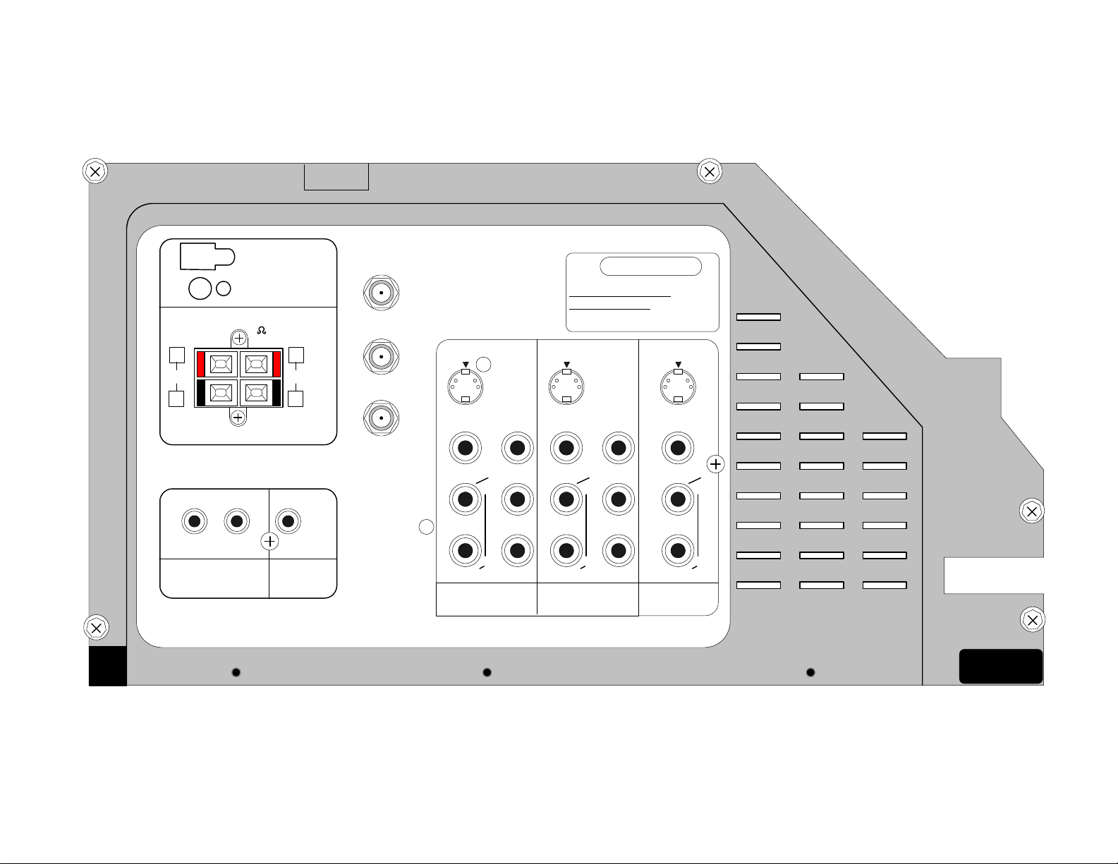
REAR PANEL for the
53SDX01B, 61SBX01B (DP-06) and 61SWX01W, 53SWX01W (DP-07)
OPTICAL
INPUT
COAXIAL
INPUT
REAR SPEAKER
8 ONLY
+
R
-
R L
AUDIO
TO HI-FI
+
L
-
SUB
WOOFER
ANT A
To
Converter
ANT B
S-VIDEO
VIDEO
(MONO)
AUDIO
INPUT 1
STOP
CONNECT ONLY 8 Ohm SPEAKERS
DO NOT SHORT CIRCUIT
THESE TERMINALS.
(such damage is NOT COVERED
by your television warranty)
Y
BCB
S-VIDEO
VIDEO
(MONO)
R
R
AUDIO
MONITOR
OUT
S-VIDEO
VIDEO
Y
BCB
R
(MONO)
AUDIO
INPUT 2
P
L
PRC
R
P
L
PRC
R
PAGE 01-07
Page 16
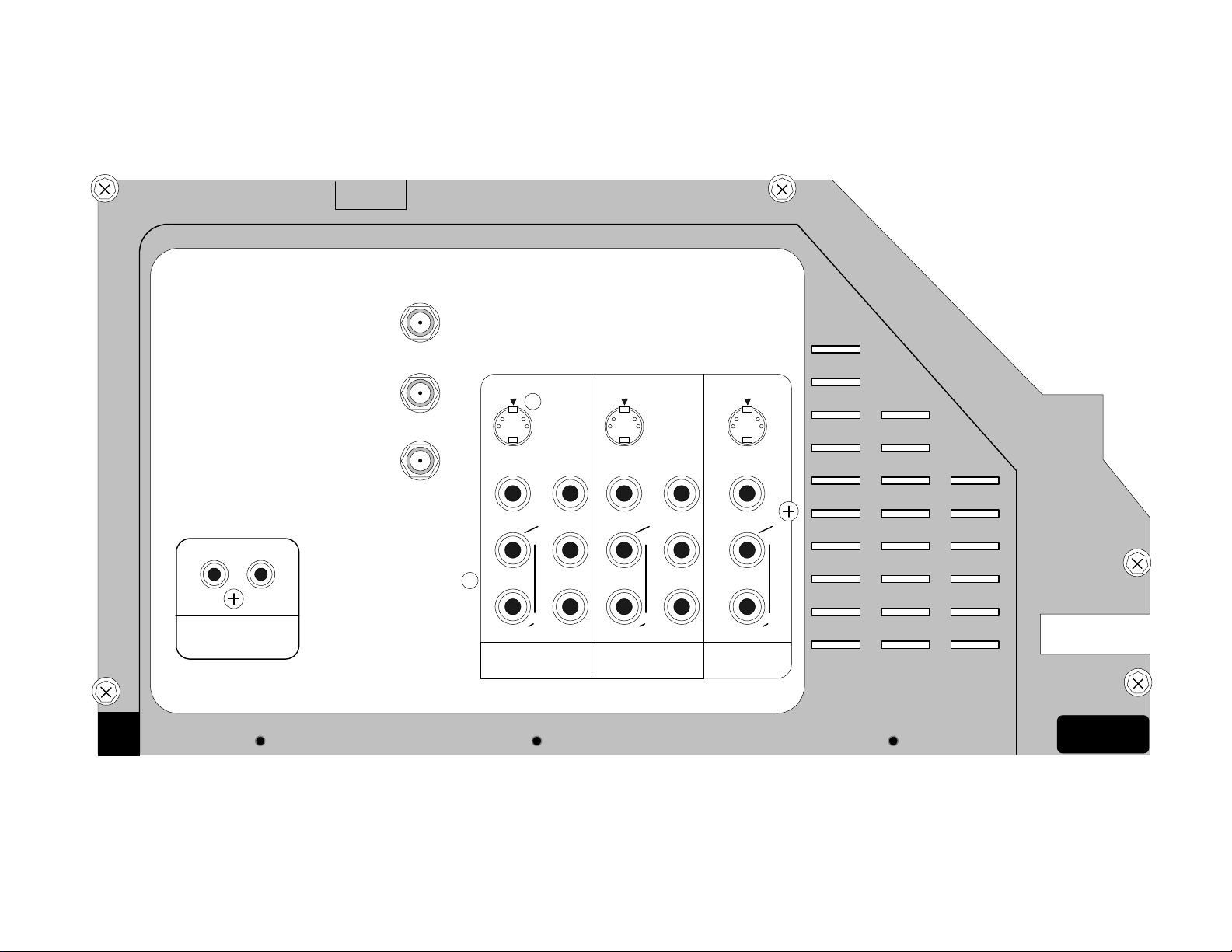
REAR PANEL for the 53FDX01B (DP-05) and 43FDX01B (DP05F)
ANT A
To
Converter
ANT B
S-VIDEO
S-VIDEO
S-VIDEO
PAGE 01-08
R
AUDIO
TO HI-FI
VIDEO
(MONO)
L
AUDIO
INPUT 1
P
L
PRC
R
Y
BCB
R
VIDEO
(MONO)
AUDIO
INPUT 2
Y
P
BCB
L
PRC
R
VIDEO
(MONO)
R
R
AUDIO
MONITOR
OUT
Page 17

MICROPROCESSOR
INFORMATION
SECTION 2
Page 18

Page 19

MICROPROCESSOR PORT DESCRIPTION
DP-0X MICROPROCESSOR PORT DESCRIPTION EXPLANATION:
The DP-0X Microprocessor is a Dual In-Line 64 pin chip. Generic number is MN102H51K. The Microprocessor
is responsible for many different operations related to the control of the Projection Television. Some of these controls are automatic and some require customer intervention, either by the Remote control or front panel keys and/
or by the customer’s menu.
When power is first applied, the Microprocessor receives it’s B+. This Microprocessor utilizes a 3.3V power supply instead of the usual 5V as in past chassis.
As the 3.3V is rising, the Reset IC (I006) holds the reset pin (54) low long enough for the main B+ to stabilize.
After stabilization, the Reset IC brings pin (54) high. During the Reset condition, the Microprocessor is initiated
into its start up state. At the same time this is happening, the Microprocessor Oscillator is generating the Microprocessor’s internal clock. The Crystal responsible for this is X001 (4Mhz) connected to pins (52 and 53). When
trouble shooting a Microprocessor for problems, it’s very important to remember the sequence described above.
Always examine the process before looking for any other problem area. The order is;
1. Vcc Applied. Generated from the Always Voltage (STY+7V I905) on the Sub Power Supply then through
the (STBY +5V I008 on the Signal PWB) to the 3.3V regulator Q026.
2. Ground is available. Look for open traces, etc….
3. The Reset circuit is working (I006). It should hold the Reset pin on the Microprocessor Low until main Vcc
is stabilized.
4. The Oscillator is running. Be careful here because a low resistance measuring probe will kill the Oscillator or
give a false reading.
After checking for the preliminary functionality of the circuits described above, then check for active clock pulses
leaving data port pins. (See the Data Communications Circuit Diagram for details). If some other IC is grounding
the data or clock pins, the Microprocessor will not work. This usually require a Pull-Up resistor. If no Pull-Up
resistor is noted in the schematic, then the responsibility for Pull-Up lies within the Microprocessor. Unloading
the pin in a good way to investigate for Pull-Up.
When a command is entered by either Remote Control, Front Keys or some internal process, the Microprocessor
runs a set of predetermined routines. These routines are hard programmed into the Microprocessor RAM and are
unchangeable. There are routine instructions that can be modified by either the customer or the Servicer and involve pre-programmed routines and variables entered by the customer or technician. These would include such
things as changing the channel , audio set-ups, on/off timer, auto-link, etc...
CONTROL OF THE PROJECTION TELEVISION:
• Receiving Infrared Remote Control Commands
• Receiving Key Input Commands
• Controlling the On and Off state of the High Voltage Power Supply.
• Interaction between the Customer’s Menu and Chassis controls.
• Outputting On Screen Display information.
• Interaction between the Servicer’s Menu and Chassis I2C Data Bus controls.
• Automatically Scanning the Tuner’s searching for Active Channels when requested by the Customer
from the Menu.
• Automatically Controlling the Tuners when Channels are changed for the Main and PinP Tuners.
• Automatically Controlling the Video Processor (Rainforest IC) when directed by the Customer.
• Controlling the Audio Circuits when directed by the Customer.
• Controlling Switching between Tuner (Main), AVX 1, 2, 3 and 4, Component 1, 2, and Tuner 2 (AUX)
or In From Converter.
The following section will explain the controls listed above.
Continued on Next Page
PAGE 02-01
Page 20

MICROPROCESSOR PORT DESCRIPTION
Continued from Preceding Page
Receiving Infrared Remote Control Commands:
Whenever the Customer utilizes the Infrared Remote, the IR receiver will detect these 38Khz Infrared pulse
train and amplify them. These pulses are delivered to the Microprocessor at Pin (1). The Microprocessor decodes
this data train and sets off the internal routine related to the command.
There is a time when the Microprocessor ignores the remote commands and that is when the Digital Convergence
Unit, (DCU here after) is in operation. The Microprocessor receives a BUSY notification that the DCU is in operation and simply doesn’t respond to remote commands. (See the Digital Convergence Interconnect Diagram and
explanation for complete details.) The BUSY signal is generated from the DCU at pin (10). Then out pin (1) of
the PSD1 connector to pin (10) of I004 DAC2. I004 sends the information via SCL1 and SDA1 lines from Pin
(14 and 15) to the Microprocessor pins (2 and 3).
Receiving Key Input Commands:
The front panel function keys are detected by the Microprocessor via R2 ladder style circuit. In other words, inside the microprocessor is a group of comparators. The function keys are strung together and each one has a different resistor value to ground. When the key is pressed, the comparators detect the change is resistance to ground
at pin (20) Clock and convert the related DC value into data the Microprocessor can understand.
The following shows the resistor value to ground from pin (20) of the Microprocessor, though pin (7) of the PFS
connector to the individual keys.
Channel Up = ground
Channel Down = 1K
Volume Up = 1K + 1.5K or 2.5K
Volume Down = 1K + 1.5K + 2.7K or 5.2K
AVX = 1K + 1.5K + 2.7K + 4.7K or 9.9K
Menu = 1K + 1.5K + 2.7K + 4.7K + 10+ or 19.9K
Controlling the On and Off state of the High Voltage Power Supply.
The Power On/Off function switch has STBY+3.3V applied for the Sub Power Supply, via pin (8) of the PFS
connector through a 1K resistor. The output of the Power On/Off switch is sent through pin (6) of the PFS to
Q014. Q014 is turned on at this time and connected to it’s Emitter is Data from the Microprocessor pin (21). The
Data is routed from Q014’s Collector to Key In pin (10) of the Microprocessor. When the Microprocessor receives this data at pin (10), it knows to turn on or off the television. This function is performed by and output
from pin (53) which controls Q002. This output from this pin is High when the set is On and Low when the set is
Off.
(For more details related to Power On/Off, see the Power On & Off Circuit Diagram Explanation and Diagram).
Interaction between the Customer’s Menu and Chassis controls.
When the Customer accesses the Main Menu, selections can be made by scrolling up and down or left to right.
Each selected input activates a set of instructions within the Microprocessor and determines the output state of
the related pins.
Outputting On Screen Display information.
When it’s necessary, the Microprocessor generates 1uSec pulses from pins (37 Red, 38 Green and 39 Blue) that
are sent to the Rainforest IC (IX01) pins (37 Blue, 38 Green and 39 Red) as OSD signals. When the OSD signals are high, they turn on the output of the Red or Green or Blue amps inside the Rainforest IC and output a
pulse to the CRTs to generate that particular character in the particular color.
(See the On Screen Display Circuit Diagram and Explanation for further details.)
(Continued on page 3)
PAGE 02-02
Page 21
MICROPROCESSOR PORT DESCRIPTION
(Continued from page 2)
Interaction between the Servicer’s Menu and Chassis I2C Data Bus controls.
When it becomes necessary for the Service Technician to make an adjustment to the set, the Service Menu must
be entered. This is accomplished with the TV turned off, then by pressing and holding the INPUT Key and then
the POWER SWITCH. The Adjustment Menu will be displayed at this time. With the Service Menu activated, the
Technician moves up and down to the desired adjustment using the Remote control or front panel Up or Down
cursor keys. To make the adjustment, the Technician uses the Remote control or front panel Left and Right cursor
Keys to change the data values for the particular adjustment.
The Microprocessor controls the individual IC related to the adjustment using I2C technology. I2C technology
allows the Microprocessor to control and IC using only two pins, (SCL and SDA).
The following pins on the Microprocessor and the ICs that it controls are described in the following table.
PINS CONTROLLED ICs
2 SDA1 and 3 SCL1 I401 AV Selector, I002 EEPROM, I003 DAC 1, I004 DAC 2
59 SDA2 and 60 SCL2 U204 3D/YC, I701 Deflection Drive, IX01 Rainforest,
IS03 Front Audio Control, IS05 Front EQ, IS10 Center EQ, IS08 Center/LFE/
PinP Audio Control, IS01 DAC3, I201 1H Main Video, and I403 H Sub Video.
57 SDA3 and 58 SCL3 IS11 Rear Audio Control.
(See the Adjustment Section for actual adjustment made in the Service Mode condition).
Automatically Scanning the Tuner’s searching for Active Channels when requested by the Customer from
the Menu.
When the Projection is first installed, the active channels must be scanned and memorized in the Channel Scan
List. This list is actually stored within the EEPROM and the Microprocessor uses the information to Scan up or
down. Held within the Microprocessor is the Initial FCC Lookup table. This table give information related to all
the channels frequency, band, and channel number. The frequency is actually a given value for the Phase Lock
Loop circuit within the tuner. Then band is data to tell the band selection circuit in the tuner where the particular
channel is located and the channel number is given to the microprocessor to indicate what OSD outputs to produce. When the set is first opened, it’s in what is called Factory Reset Condition. For the Tuner this means that
the signal source is AIR, and channels 2 through 13 are in the channel scan list. Before the customer runs Auto
Program, they must set the signal source to the type they are using, Air, Cable 1 or Cable 2. After the source is
set, the customer then proceeds with Auto Programming.
When Auto Programming is initiated, the Microprocessor has a specific program to run. This program starts by
placing the tuner in the lowest channel in the lowest band. That would normally be channel 2. Then the program
instruct the Microprocessor to look for Sync. To do this, the Microprocessor actually need Horizontal Blanking
(H.Blk) at pin (49) which is labeled H.Sync and Video Sync (24) labeled Main/Sub SD Det.
Horizontal Blanking is use as a gate pulse for the coincidence detector. Within the coincidence detector is a circuit that looks at the timing of the Sync in relationship to (H.BLK). If the signal being checked is not in time with
(H.Blk). The signal is ignored. However, if the signal being monitored is in coincidence with (H.Blk) the signal
is deemed to be true Video Sync and that particular channel is stored as an active channel in the EEPROM Scan
List.
Then the Microprocessor sends information to the tuner to move up one channel and the whole process begins
again. This is repeated until every channel is checked. After completion of the scan, the microprocessor retrieves
information from the EEPROM concerning the first channel in the lowest band that appears in the scan list and
directs the tuner to tune to that channel.
(Continued on page 4)
PAGE 02-03
Page 22
MICROPROCESSOR PORT DESCRIPTION
(Continued from page 3)
Automatically Controlling the Tuners when Channels are changed. (See Figure 1)
MAIN TUNER:
When channels are changed, the Microprocessor runs another routine. This routine detects the command if it’s
input by the Remote Control or the Front keys, whether it’s Scan Up/Down or direct access, and begins to control
the Tuner. First the Microprocessor output a Mute command to blank the video, then data is sent to the tuner to
move it to the desired channel. After that the Microprocessor again checks the coincidence detector for active
sync. If active sync is detected, the Microprocessor opens what is called the AFC Loop. The AFC Loops comprises two cycles trying to lock the tuner to the specific IF frequency of 45.5 Mhz. A DC voltage is sent from either the Main Tuner U201 pin (10) or the PinP Tuner U202 pin (21) back to the Microprocessor pin (6). This
DC voltage indicates the error between the IF detected and the IF frequency reference. This error voltage tells the
Microprocessor to do one of two things. 1st, if the error is large, the Microprocessor changes the Programmable
Divider’s division rate to a larger or smaller degree to get closer to the actual IF frequency desired. Or 2nd move
the Pulse Swallow division rate to either 1/32 or 1/33. The Pulse Swallow tuning circuit is a second divider that is
on the output from the Prescaler. The main Prescaler takes the very high frequency output from the tuners mixer
circuit which is produced when the tuners main oscillator is beat against the incoming RF frequency. The Programmable Divider is instructed by the Microprocessor exactly what division rate to apply to the Beat Frequency
generating the IF frequency. The IF frequency is then sent through the Pulse Swallow circuit which again divides
the IF frequency at a much smaller rate . This allows the IF output frequency to become much more finite and can
correct for much smaller errors between the Phase comparators reference frequency. The error voltage generated
is directed back to the main internal Oscillator in the front end and corrects for Tuning errors.
(See the Microprocessor Data Communications Circuit Diagram Explanation for Details related to Data Communication for controlling the Main Tuner).
INTEGRATED TUNER
RF
BM (B+ Mains)
Tuning
Voltage
+33V
Mix
Band
Tuning
Voltage
Main
Osc
B+ Distribution
Pre-
Scaller
Fixed
Programm-
IF Out IF In
Pulse
able
Divider
Interface
Data Clock Load AFC
Swallow
1/32 or
1/33
Phase
Comparator
Comparator
MAIN
MICROPROCESSOR
Video Det
Error
Amp
IF
Video
5K
Ref
Osc
Ref
Freq.
45.5K
Figure 1
(Continued on page 5)
PAGE 02-04
Page 23
MICROPROCESSOR PORT DESCRIPTION
(Continued from page 4)
Automatically Controlling the Tuners when Channels are changed. (See Figure 1)
PinP TUNER:
As far as the internal function of the PinP Tuner, it is the same as the Main Tuner.
(See the Microprocessor Data Communications Circuit Diagram Explanation for Details related to Data Communication for controlling the Main Tuner).
When the customer presses the PinP button on the Remote Control, the Microprocessor outputs Clock, Data and
Enable controls to the Flex Converter. The Flex Converter also has the PinP circuit inside. The Clock, Data and
Enable pins on the Microprocessor are pins (20 Clock, 21 Data and 46 FCENABLE) These are routed to the
Level Shift IC, I014 pins (2, 3 and 4). They are output on pins (18, 17 and 16) to the Flex Converter U205 connector PFC1 and input on pins (10, 11 and 12). The Flex Converter’s PinP unit is then switched on and insertion
is made into the regular Main Video line. The position of the PinP window, the PinP window itself and other different display conditions are controlled by this process. When SWAP is pressed on the remote control, the channel or input that the PinP tuner was on, now becomes the Main Video’s source and the channel or input that the
Main signal was on, now becomes the PinP source.
Automatically Controlling the Video Processor (Rainforest IC) when directed by the Customer.
The Rainforest IC has many enhancement circuits built in. These would include the Black Peak Expansion circuit,
the Dynamic Noise Reduction circuit, Time Compression and of course Sharpness, Black Level and Contrast adjustments as well.
• Black Peak Expansion Circuit:
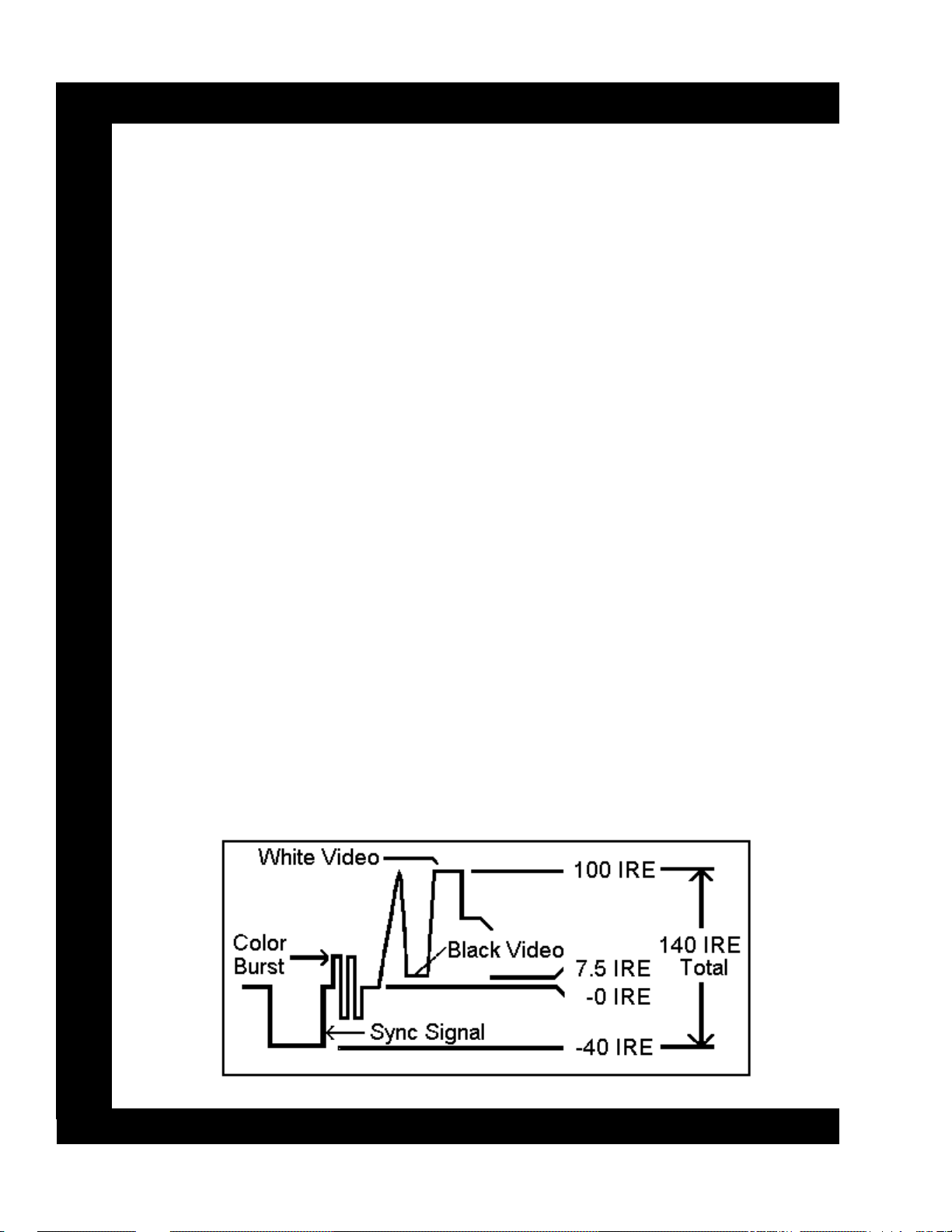
This circuit is utilized to increase the contrast ratio. The standard video signal is 1 Volt Peak to Peak (p/p
hear after), the actual video (Y) content is 730mVp/p. The 1 Vp/p is explained it IRE figures from this
point on. The Standard video signal is divided into units called IRE. The units are equal to 140 total for
the 1Vp/p signal. Sync occupies 40IRE which are negative. And the Luminance represents 100 IRE
units. Each unit represents 7.1428mVp/p of information. (See Figure 2 below.)
The Black Peak Expansion circuit monitors the 1/2 way point of luminance, (50 IRE or 357mV) and
pulls the signal towards pure black or the 7.5 IRE level. This increases the distance from Black Peak to
White Peak which is contrast.
• Dynamic Noise Reduction Circuit:
This circuit again monitors the area from 50 IRE down and subtracts noise. This circuit is dynamic
meaning that it characteristics change. In other words, the subtraction process is greater near black level
that it is near 50 IRE. The subtraction is 6dB at maximum, meaning that there would be some frequency
loss near black, but the noise which is seen as white speckles would be reduced.
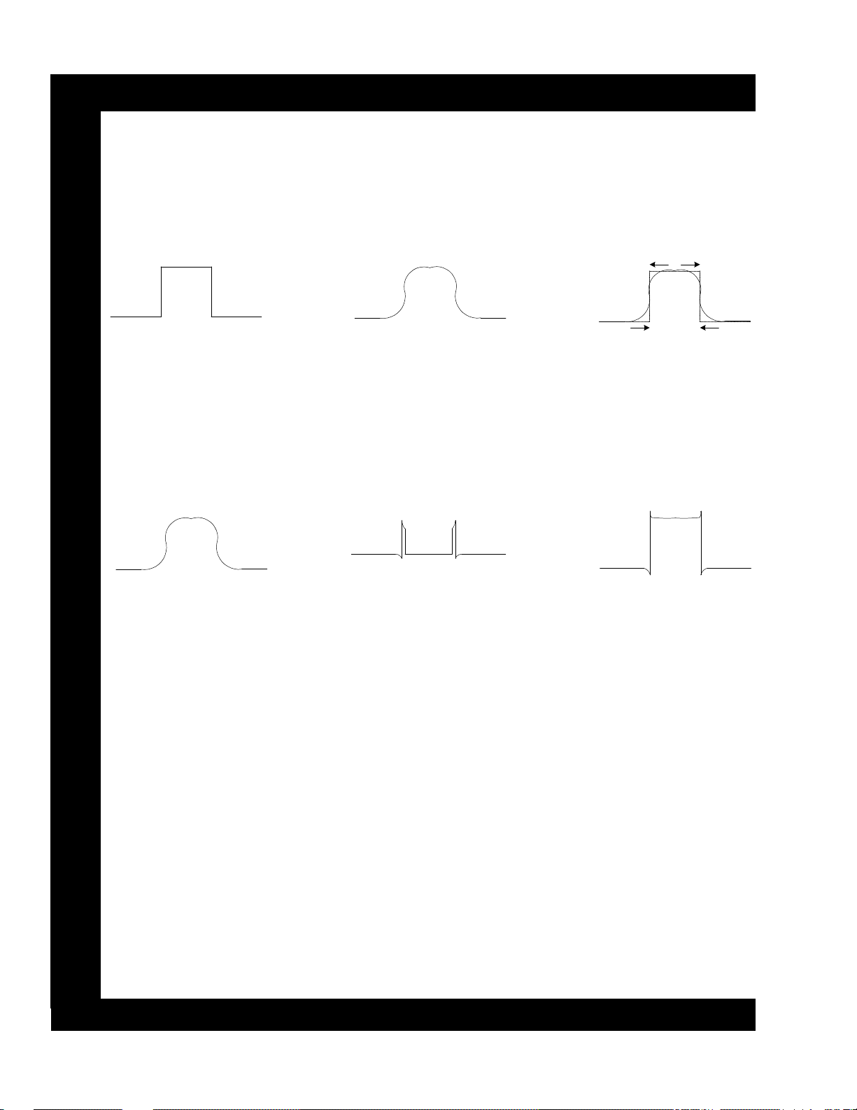
• Time Compression Circuit:
Any time an analog signal is passed through a capacitive circuit, its high frequencies are reduced. To replace these high frequencies, Hitachi uses Time Compression. This circuit is on the order of Aperture
Compensation, however it differs in the fact that it uses 5 delay lines. The actual signal should look like
Figure 2
(Continued on page 6)
PAGE 02-05
Page 24
MICROPROCESSOR PORT DESCRIPTION
(Continued from page 5)
Figure 3, however after passing through a capacitive circuit, it looks like Figure 4. After Time Compression takes place, the beginning rise is advanced. Just before white peak the signal is delayed. Just before
the signal falls the signal is advanced and just before the signal reaches black peak the signal is delayed.
This causes the signal to appear more like the actual signal and thus restores the high frequencies lost
through capacitance.
Actual Signal After passing through a capacitor
Figure 3
Figure 4
After Time Compression
Figure 5
• Sharpness:
During the Time Compression process, switching pulses that are detected at the transition point, (A tran-
sition is the point at which the luminance signal goes for black to white or white to black) are used in the
sharpness circuit.. This signal is the routed through a sort of variable resistor and according to how much
sharpness the customer has selected, determines how much of the transition signal is added to the original signal. The greater the sharpness setting, the greater the transition signal added.
Original Signal Transition Point pulses
Figure 6
Figure 7
Transition Pulses Added
Figure 8
Controlling the Audio Circuits when directed by the Customer.
The customer has control over how the set accesses audio information for all of it’s inputs. The tuner for example
is an integrated type. This not only means that held within the Main Tuner are all the necessary components for
Reception and Video detection. It also has a built in audio and MTS decoder. The Main Tuner outputs Left Total
and Right Total signals. (Left Total and Right Total means that the encoding for Pro-Logic is held within the indi-
vidual signal.) The customer can select first of all, how the Tuner decodes it’s audio. Stereo, Mono, or SAP can
be selected. The Main Tuner must tell the Microprocessor what signal it is receiving. The Main Tuner has a ST
LED output at pin (19) which tells the Microprocessor it is receiving MTS Stereo and a SAP LED output at pin
(20) which tells the Microprocessor it is receiving Second Audio Program. How these are selected by the consumer via the Main Menu determines the output from the Microprocessor.
• ST LED is routed from the Main Tuner at pin (19), through Q204, to the DAC1 I003 pin (10). The DAC1
outputs Clock and Data via pins 15 SCL1 and 14 SDA1 signals to the Microprocessor input on pins 3 SCL1
and 2 SDA2. The Microprocessor knows how to switch the tuners decoder circuit by making judgment upon
these inputs. Then the Microprocessor can use Clock, Data and Enable lines to control the Tuner.
(Continued on page 7)
PAGE 02-06
Page 25

MICROPROCESSOR PORT DESCRIPTION
(Continued from page 6)
• SAP LED is routed from the Main Tuner at pin (20), through Q203, to the DAC1 I003 pin (9). The DAC1
outputs Clock and Data via pins 15 SCL1 and 14 SDA1 signals to the Microprocessor input on pins 3 SCL1
and 2 SDA2.
The Microprocessor knows how to switch the tuners decoder circuit by making judgment upon these inputs. Then
the Microprocessor can us Clock, Data and Enable lines to control the Tuner.
Clock, Data and Enable lines for the Main Tuner are output from the Microprocessor at pins (20, 21 and 44) respectively. Pin (44) FEENABLE1 goes directly to the Main Tuner at pin (6), where as the Clock and Data lines
must be routed through the Level Shift IC I014 to be brought up to 5V. Clock and Data arrive at I014 at pins (2
and 3) and are output at pins (18 and 17). They arrive at the Main Tuner at pins (4 and 5).
The PinP Tuner doesn’t have MTS capability. It only output mono audio, so no switching takes place for the PinP
Tuner U202 audio circuit. The only difference for the PinP tuner control lines is related to the PinP Enable line.
This is output from the Microprocessor pin (43 FEENABLE2) to the PinP Tuner at pin (17). Clock and Data are
the same as for the Main Tuner.
(See Microprocessor Data Communications Circuit Diagram and Explanation for further details).
Controlling Switching between Tuner (Main), AVX 1, 2, 3 and 4, Component 1, and 2, and
Tuner 2 (AUX) or In From Converter.
The different inputs can be selected by the Remote Control or the Front Panel switches. This is accomplished by
the INPUT button. Each time the Input button is pressed, the different inputs are sequentially selected. The sequential order is, Main Tuner, AVX 1, AVX 2, AVX 3, AVX 4, 2nd Antenna and back to Main Tuner. Also, if
there are S-Inputs on AVX1, 2 or 4, there is an internal mechanical switch inside the S-Jack that tells the Microprocessor an S-Jack is inserted. Then when that particular input is selected, it automatically selects S as it’s
source. The same thing holds true for Component inputs. The set should never have Component inputs and S-Jack
inserted at the same time and a black and white picture will be displayed.
(See Video Signal Processing for details related to Video Switching.)
PAGE 02-07
Page 26
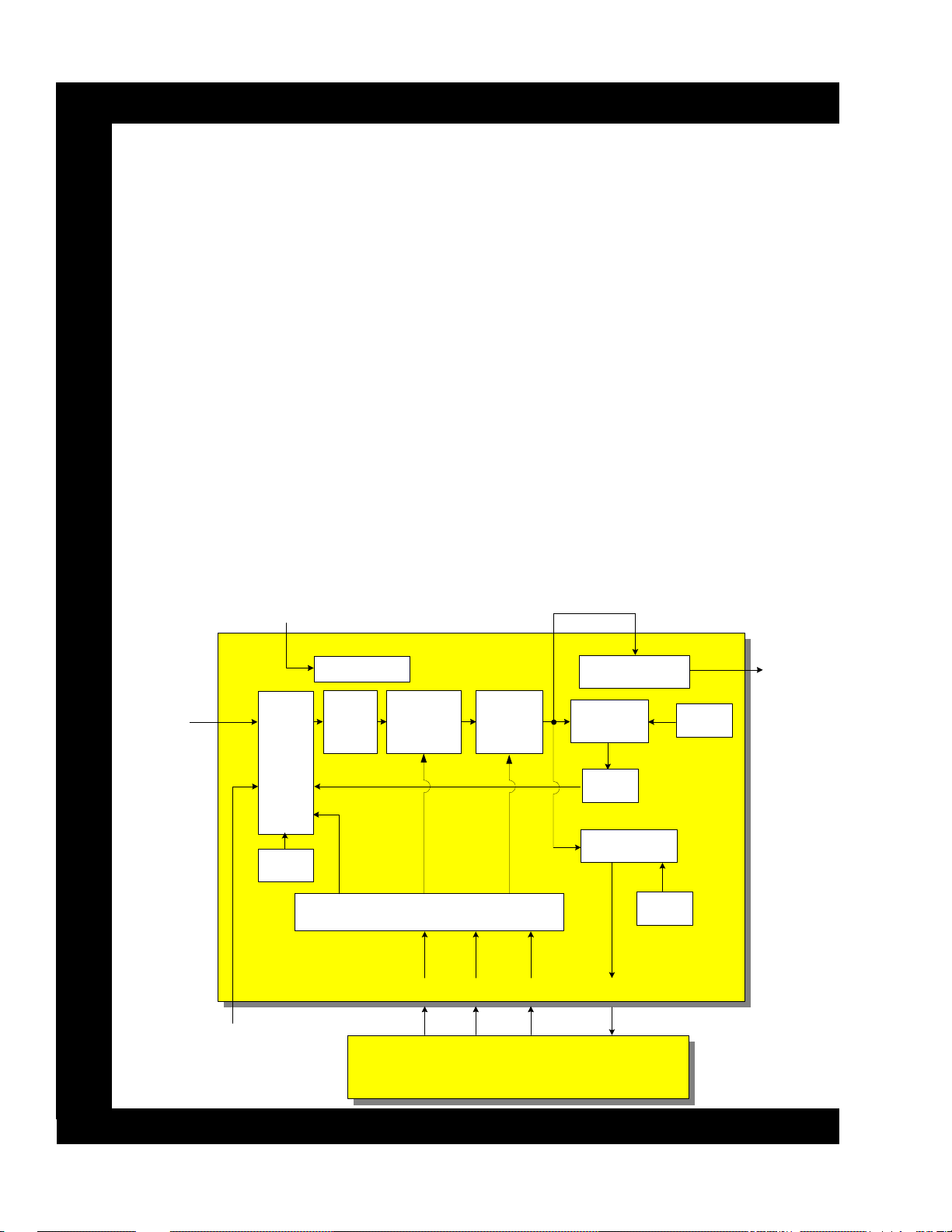
DP-0X CHASSIS MICROPROCESSOR I-001 PIN/PORT DESCRIPTION 1 through 35
Pin No. ID Function Active
1 IRIN Receives Remote Control Inferred pulses. Data
2 SDA1 Serial Data Sent and Received from the EEPROM, A/V Selector, DAC1, DAC2. Function of I2C. Data
3 SCL1 Serial Clock Synchronization Sent to the EEPROM, A/V Selector, DAC1, DAC2. Function of I2C. Data
4 Dimmer Receives DC voltage generated from the Photo Receiver on the Front Panel monitoring Room Light. For AI DC
5 AD Key In Receives Level Shifted DC voltage from Front Panel Key presses. DC
6 Main/Sub AFC Receives the Main Tuner AFC or Sub AFC DC Voltage switched by I005. Used during channel change. DC
7 Key In When the Power switch is pressed, Clock data from pin 21 is routed through Q014 back to this pin. Power is toggled On or Off. Data
8 Not Used Not Used N/A
9 Not Used Not Used N/A
10 Main FV Det Receives Composite 1 V Sync from I015 pin 4 for OSD Positioning. Sync
11 Sub FV Det Receives Composite 2 V Sync from I016 pin 4 for OSD Positioning. Sync
12 DSP Busy Receives the Busy command from the Digital Surround Processor on the Surround PWB. DC
13 DSP SO Control command to the DSP Unit for controlling Modes. Data
14 DSP Dir Receives Digital Surround Processor Error information from the DSP unit on the Surround PWB. Data
15 DSP SS Control command to the DSP Unit for controlling Modes. Data
16 DSP SCK Digital Surround Processor Clock. Data
17 DSP S1 Control command to the DSP Unit for controlling Modes. Data
18 DSP ERR Mute Mutes Audio when a DSP Dir input is detected. (DSP Error). DC High
19 DSP Reset Resets the DSP module on the Surround PWB DC High
20 Clock Sent to the Level Shift I014 then to both Tuners and the Flex Converter as a timing signal. Also see pin 7. Data
21 Data Sent to the Level Shift I014 then to both Tuners and the Flex Converter to control each unit. Data
22 Comp 1/2 FH Det Either Component One or Two Horizontal Input from I005 through Q046. Used for OSD Display. And Auto Link DC
23 AC In Receives Timing pulses for advancing the Clock. Received from the Smitt Amp Q008 and Q009 60Hz.
24 Main/Sub SD Det Station Detection. Used during Auto Programming and when channels are changed to open AFC Loop. Switched by I005. Sync
25 VDD Stby +3.3V generated by 0029. Main Microprocessor B+. DC
26 CHL Clamp level High DC
27 VRefFHS Use as a reference signal within the Microprocessor High Frequencies. DC
28 CVBS0 Composite Sync used for Closed Caption Detection for the Main Tuner. Sync
29 VSS Ground N/A
30 CVBS1 Not Used. Composite Sync used for Closed Caption Detection for the PinP Tuner. N/A
31 VREFLS Reference Signal used within the Microprocessor Low Frequencies. N/A
32 CLL Internal function of the Microprocessor. N/A
Page 02-08
33 AVDD Stby +3.3V generated by 0029. DC
34 COMP Internal function of the Microprocessor. DC
35 IREF Internal function of the Microprocessor. DC
Page 27
DP-0X CHASSIS MICROPROCESSOR I-001 PIN/PORT DESCRIPTION 36 through 64
Pin No. ID Function Active
36 VREF Internal function of the Microprocessor. DC
37 OSD R Outputs Red characters for the Service Menu. Data
38 OSD G Outputs Green characters for the Service Menu. Data
39 OSD B Outputs Blue characters for the Service Menu. Data
40 HALF TONE Controls the Translucency of the Main Menu Background. Low = Clear, Mid = Transparent, Hi = Gray. Data
41 PDO Internal function of the Microprocessor. DC
42 BVC0I Internal function of the Microprocessor. DC
43 FE ENABLE 2 Front End Enable. Enables the reception of data from the Microprocessor by the PinP Tuner. Data
44 FE ENABLE 1 Front End Enable. Enables the reception of data from the Microprocessor by the Main Tuner. Data
45 V.MUTE Mutes Audio and Video through Q008 and Q010 to Sub Video and Surround PWB during channel change. High = Mute DC
46 FC ENABLE Flex Converter Enable Line. Allows the Flex Converter to receive commands from the Microprocessor. Data
47 OSD X0 Reference Frequency for OSD. Determines the OSD Size. Data
48 OSD X1 Reference Frequency for OSD. Determines the OSD Size. Data
49 H SYNC Receives Horizontal Blanking pulses 3.3Vp/p for OSD positioning. Generated from H Blk through Q006 H Blk
50 SD SELECT Sent through Q030 to I015 for setting the internal selection switches. Hi = Main, Lo = Sub DC
51 OSD BLK Outputs a pulse slight wider and in time with the OSD characters to clean up video where character will be displayed. Data
52 TEST Use by the factory for internal test of the Microprocessor and to place in a specific set of criteria. DC
53 Power ON/OFF This output goes high when the Power Button is pressed for ON and Low for Off. DC
54 RESET Low when Power first applied then rises to a high of 3.3V. Received from I006. Resets the Microprocessor. DC
55 VSYNC Receives Vertical Blanking pulses 3.3Vp/p for OSD positioning. Generated from V Blk through Q005 Data
56 P BLK Sent to the Rainforest IC IX01. Used to Mute the Video during Channel change, Child Lock, AVX selected with no input. Hi = Mute DC
57 SDA3 Serial Data Sent to the Rear Audio Output IC IS11 on Surround PWB. Controls Volume, Bass, Treble, and Bal. Function of I2C. Data
58 SCL3 Serial Clock Sent to the Rear Audio Output IC IS11 on Surround PWB. Used for Timing of Data. Function of I2C. Data
59 SDA2 Serial Data Sent to U204, I701, IX01, IS03, IS05, IS10, IS08, IS01, I201 and I403. Function of I2C. Data
60 SCL2 Serial Clock Sent to U204, I701, IX01, IS03, IS05, IS10, IS08, IS01, I201 and I403. Function of I2C. Data
61 VDD Stby +3.3V generated by 0029. Main Microprocessor B+. DC
62 OSC In OSC In (4MHz) Data
Page 02-09
63 OSC Out OSC Out (4MHz) Data
64 VSS Ground. N/A
Page 28
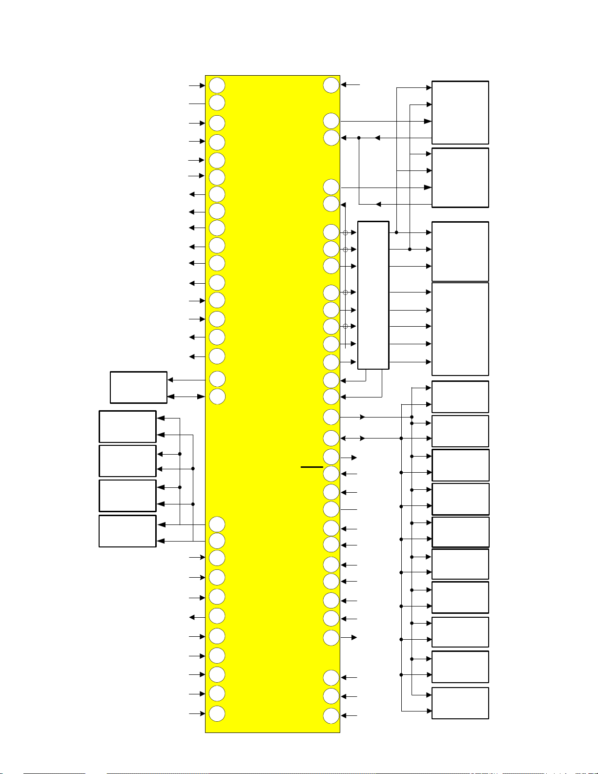
DP0X SYSTEM CONTROL PORT DESCRIPTION
I001
Dimmer
POO
VSS (Gnd)
AC In
OSD X1
OSD Xo
OSD B
OSD R
OSD G
Half Tone
OSD Blk
Power On/Off
VRef
B+Fail
P Blk. 56
VMute
41
29
23
48
47
39
37
38
40
51
53
36
45
4
9
VDD (3.3V)
FE Enable1
Main/Sub AFC
FE Enable2
FC Enable
DSP SI
DSP Err Mute
DSP Sck
DSPSS
DSPRST
Key In
Clock
Data
61
44
6
43
7
20
21
46
17
18
16
15
19
Power Switch
I014
Level
Shift
CLOCK
DATA
ENABLE
AFC
DATA
CLOCK
ENABLE
AFC
Clock
Data
Enable
DSP SI
DSP Err
DSP Sck
DSPSS
DSPRST
U201
MAIN
TUNER
U202
PinP
TUNER
U205
Flex Conv & PinP
Unit
Audio DSP
AC3/ProLogic
Rear Audio
Control
A/V
Selector
EEPROM
DAC 1
DAC 2
Main V. Chip Data and CCD
IS11
I401
I002
I003
I004
Sub V. Chip Data
Ft. Panel Control Keys
SDA
SCL
SCL
SDA
SCL
SDA
SCL
SDA
SCL
SDA
VSS (Gnd)
OSC In
OSC Out
IRIn
VRefHS
CLH
57
58
28
30
62
63
64
27
26
SDA3
SCL3
3
SCL1
2
SDA1
1
AD
5
KeyIn
Main/Sub SD Det
DSP S0
DSP Busy
SCL2
SDA2
SO Select
Reset
IRef
BVCOI
AVDD 3.3V
Test
CLL
Sub FV Det
Main FV Det
Comp
G+Reset
VSync
H.Blk/H.Sync
13
12
60
59
50
54
35
42
33
52
32
11
10
34
55
49
24
SCL
U204
SDA
SCL
SDA
SCL
SDA
SCL
SDA
SCL
SDA
SCL
SDA
SCL
SDA
SCL
8
N/C
SDA
SCL
SDA
SCL
SDA
I201
I403
I701
IX01
IS03
IS05
IS05
IS10
IS08
IS01
3D/YC
Comb Filter
Deflection
Rainforest
IC
Front Audio
Control
Front EQ
Cent EQ
Cent/LFE/
Audio Control
DAC3
1 H Main Video
1 H Sub Video
PAGE 02-10
Page 29

DP-05 and DP-05F MICROPROCESSOR PORT DESCRIPTION
DP-05F PORT DESCRIPTION
Refer to the DP-05 and DP-05F System Control Port Description Circuit Diagram
The only difference between the DP-05 & DP-05F and the DP-06 or DP-07 System Control Port Description Circuit Diagram is;
The DP-05 and DP-05F doesn’t have the DSP Module. Therefore, it uses a SRS Surround PWB. There is no
•
Rear or Center Audio, so the Serial Data Communications (
Used.
The Data Communications to the Level Shift IC (
•
The Rear Audio IC, Center Audio IC and the Center Graphic EQ IC are not used.
•
The Front Audio Control IC designation is (
•
The DAC3 IC designation is (
•
All else remains the same.
(See Next page for diagram).
).
IA01
IA05
) going to the (DSP) is not used.
I014
).
SCL3
and
) to the Rear Audio B+ isn’t
SDA3
PAGE 02-11
Page 30
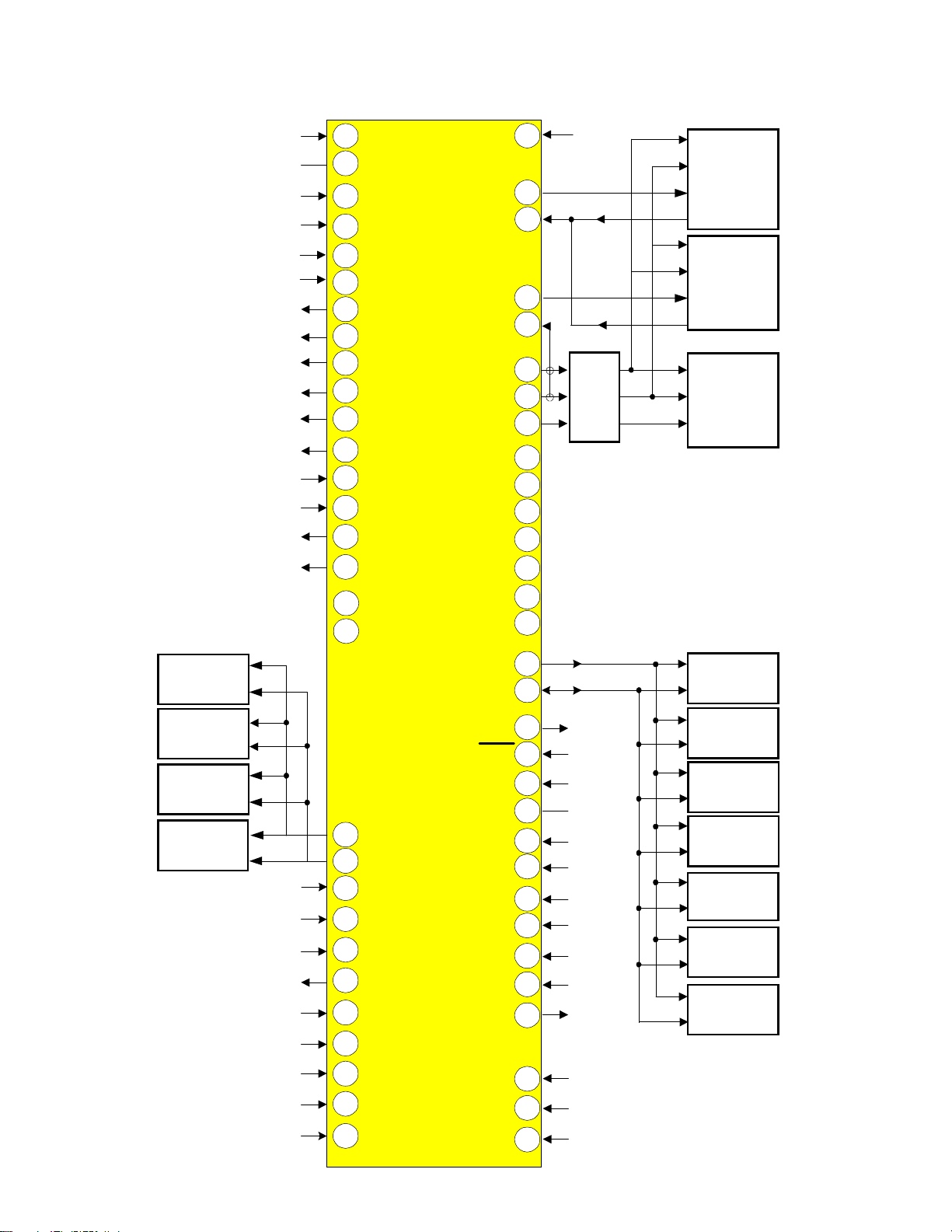
DP-05 and DP-05F SYSTEM CONTROL PORT DESCRIPTION
I001
Clock
Data
61VDD (3.3V)
44
6
43
7
20
21
46
Power Switch
I014
Level
Shift
CLOCK
DATA
ENABLE
AFC
DATA
CLOCK
ENABLE
AFC
Clock
Data
Enable
Dimmer
POO
VSS (Gnd)
AC In
OSD X1
OSD Xo
OSD B
OSD R
OSD G
Half Tone
OSD Blk
41
29
23
48
47
39
37
38
40
51
4
FE Enable1
Main/Sub AFC
FE Enable2
Key In
FC Enable
U201
MAIN
TUNER
U202
PinP
TUNER
U205
Flex Conv &
PinP Unit
A/V
Selector
EEPROM
DAC 1
DAC 2
I401
I002
I003
I004
Main V. Chip Data and CCD
Power On/Off
VRef
B+Fail
P Blk.
VMute
SCL
SDA
SCL
SDA
SCL
SDA
SCL
SDA
Sub V. Chip Data
OSC In
OSC Out
VSS (Gnd)
IRIn
N/A
N/A
53
36
56
45
57
58
28
30
62
63
64
17
18
16
15
19
13
12
60
59
50
54
35
42
33
52
32
11
10
34
N/A
N/A
N/A
N/A
N/A
N/A
N/A
SCL
U204
SDA
SCL
SDA
SCL
SDA
SCL
SDA
SCL
IA01
SDA
SCL
I201
SDA
SCL
8
N/C
I403
SDA
I701
IX01
IA05
3D/YC
Comb Filter
Deflection
Rainforest
IC
Front Audio
Control
DAC3
1 H Main Video
1 H Sub Video
DSP SI
DSP Err Mute
9
SDA3
SCL3
3
SCL1
2
SDA1
1
DSP Sck
DSPSS
DSPRST
DSP S0
DSP Busy
SCL2
SDA2
SO Select
Reset
IRef
BVCOI
AVDD 3.3V
Test
CLL
Sub FV Det
Main FV Det
Comp
G+Reset
VRefHS
CLH
Ft. Panel Control Keys
27
26
55
VSync
H.Blk/H.Sync
AD
5
KeyIn
Main/Sub SD Det
49
24
PAGE 02-12
Page 31

MICROPROCESSOR DATA COMMUNICATION DESCRIPTION
Use this explanation in conjunction with the Microprocessor Data Communications circuit diagram.
The Microprocessor must keep in communication with the Chassis to maintain control over the individual circuits. Some of the circuits must return information as well so the Microprocessor will know how to respond to
different request.
The Microprocessor uses a combination of I2C Bus communication and the Serial Data, Clock and Load lines for
control. The I2C communication scheme only requires 2 lines for control. These lines are called SDA and SCL.
Serial Data and Serial Clock respectively.
The Microprocessor also requires the use of what are called Fan Out IC or DACs, (Digital to Analog Converters).
This allows the Microprocessor to use only two lines to control many different circuits.
Also, due to the fact that this Microprocessor operates at the new 3.3Vdc voltage, it requires a Level Shift IC to
bring up the DC level of the control lines to make it compatible with the connected ICs.
The Microprocessor communicates with the following ICs:
ON THE SIGNAL PWB:
Main Tuner U201
PinP Tuner U202
EEPROM I002
Flex Converter U205
DAC1 I003
DAC2 I004
Level Shift I014
3D Y/C U204
Main Video Chroma I201
ON THE TERMINAL PWB:
A/V Selector I401
Sub Video Chroma I403
ON THE DEFLECTION PWB:
Sweep Control I701
ON THE SUB VIDEO PWB (2H VIDEO):
Rainforest IX01
ON THE SURROUND PWB:
Front Audio Control IS03
Center/LFE (Low Frequency Effects) Audio Control IS08
Surround Board DAC3 IS01
Front Equalizer IS05
Center Equalizer IS10
Rear Audio Control IS11
Audio DSP (Digital Signal Processor) DSP Unit HC4051
The following explanation will deal with the communication paths used between the Microprocessor and the respected ICs.
ON THE SIGNAL PWB:
Main Tuner U201
The Microprocessor controls the Main Tuner by Clock, Data and Enable lines.
Clock, Data and Enable lines for the Main Tuner are output from the Microprocessor at pins (20 Clock, 21 Data
and 44 FEENABLE1) respectively. Pin (44) FEENABLE1 goes directly to the Main Tuner at pin (6), where as
the Clock and Data lines must be routed through the Level Shift IC I014 to be brought up to 5V. Clock and Data
from the Microprocessor arrive at I014 (Level Shift) at pins (2 and 3) and are output at pins (18 and 17).
They arrive at the Main Tuner at pins (4 and 5).
(Continued on page 14)
PAGE 02-13
Page 32

MICROPROCESSOR DATA COMMUNICATION DESCRIPTION
(Continued from page 13)
PinP Tuner U202
The only difference for the PinP tuner control lines is related to the PinP Enable line. This is output from the
Microprocessor pin (43 FEENABLE2) to the PinP Tuner at pin (17). Clock and Data are the same as for the
Main Tuner.
For further details about tuner operation, please see the Microprocessor Port Description and Circuit Diagram.
EEPROM I002
The EEPROM is ROM for many different functions of the Microprocessor. Channel Scan or Memory List,
Customer set ups for Video, Audio, Surround etc… are memorized as well. Also, some of the Microprocessors
internal sub routines have variables that are stored in the EEPROM, such as the window for Closed Caption
detection.
Data and Clock lines are SDA1 from pin (2) of the Microprocessor to pin (5) of the EEPROM and SCL2 from
pin (3) of the Microprocessor to pin (6) of the EEPROM. Data travels in both directions on the Data line.
Flex Converter U205
The projection television is capable of two different horizontal frequencies. 31.5Khz for everything except HD
and 33.75Khz for HD. (High Definition). The Flex Converter is responsible for receiving any video input and
converting it to the related output. This output is controlled by sync and by the customer’s menu and how it is
set up. The set up can be 4X3 or 16X9 sometimes called letterbox. The Flex Converter can take any NTSC, SIn, Component in in NTSC, Progressive, Interlaced, 480I, 720P, 1080I signal.
Control for the Flex Converter is Clock, Data and Enable lines.
Clock, Data and Enable lines for the Flex Converter are output from the Microprocessor at pins (20 Clock, 21
Data and 46 FCENABLE). FCENABLE Clock and Data lines must be routed through the Level Shift IC
I014 to be brought up to 5V. They arrive at I014 at pins (2 Clock, 3 Data and 4 FCENABLE) and are output
at pins (18, 17 and 16) respectively.
DAC1 I003
This Digital to Analog converter acts as an extension of the Microprocessor. Sometimes called an Expansion
IC. The purpose of this IC is to reduce the number of pins, (fan out) of the Main Microprocessor I001. The
Main Microprocessor send Clock and Data via I2C bus to the DAC1 IC. The output from the Microprocessor is
pin (2 SDA1 and 3 SCL1) which arrives at the DAC1 IC at pins (5 and 6) respectively.
The following is a list of the input and output pins on DAC1.
PIN FUNCTION
1 IR Det The IR pulse from the Remote Control is monitored when Auto Link is set. (See Auto Link in Index).
2 YN Det Active Low. This pin monitors for active sync when Auto Link is set. (See Auto Link in Index).
3 Blk Main Normal High, Blanking Low. Blanks Y-Cb/Cr into Flex Converter.
4 MTS Places the Main Tuner pin (21 mode) into MTS Stereo. If Tuner receiving MTS signal. See pin 10.
5 F Mono Places the Main Tuner pin (22 mono) into forced Mono Mode.
6 Ant Switches the antenna block into Antenna A or Antenna B when selected.
7 Blk Sub Normal High, Blanking Low. Blanks PinP Sub Y-Cb/Cr on Terminal PWB before going into Flex Converter.
8 Gnd Ground
9 SAP Det The Main Tuner outputs an SAP LED signal when SAP is detected. Active Low.
10 ST Det The Main Tuner outputs an ST LED signal when Stereo is detected. Active Low.
11 SAD0 Ground Not Used
12 SAD1 Ground Not Used
13 SAD2 Ground Not Used
14 SDA Data I2C communications between DAC1 and Microprocessor
15 SCL Clock I2C communications between DAC1 and Microprocessor
16 Vcc IC B+. (STBY +5V)
(Continued on page 15)
PAGE 02-14
Page 33

MICROPROCESSOR DATA COMMUNICATION DESCRIPTION
(Continued from page 14)
DAC2 I004
This Digital to Analog converter acts as an extension of the Microprocessor. Sometimes called an Expansion
IC. The purpose of this IC is to reduce the number of pins, (fan out) of the Main Microprocessor I001. The
Main Microprocessor send Clock and Data via I2C bus to the DAC2 IC. The output from the Microprocessor is
pin (2 SDA1 and 3 SCL1) which arrives at the DAC2 IC at pins (5 and 6) respectively.
The following is a list of the input and output pins on DAC2.
PIN FUNCTION
1 YUV Det1 Detects activity on Component Input number 1.
2 YUV Det2 Detects activity on Component Input number 2.
3 FH Det Out 1 Test Point 1 (TP1).
4 Sel5 Controls IX02 on 2H PWB. Selects either Y Cb/Cr or Y IQ to compensate for Chroma Phase angle used in Auto Color.
5 F Mono Places the Main Tuner pin (22 mono) into forced Mono Mode.
6 FH Det Out 1 Test Point 2 (TP2).
7 31/33 Notifies the DCU related to Horizontal Frequency. Either 31.5Khz for everything but HD or 33.75Khz for HD.
8 Gnd Ground
9 CS Sel Not Used.
10 Busy Informs the Microprocessor that the DCU is in the Digital Convergence Adjustment Mode. The Micro. Ignores IR pulses.
11 SAD0 Ground Not Used
12 SAD1 Ground Not Used
13 SAD2 IC B+. (STBY +5V).
14 SDA Data I2C communications between DAC2 and Microprocessor
15 SCL Clock I2C communications between DAC2 and Microprocessor
16 Vcc IC B+. (STBY +5V).
Level Shift I014
The Microprocessor operates at 3.3Vdc. Most of the Circuits controlled by the Microprocessor operate at 5Vdc.
The Level Shift IC steps up the DC voltage to accommodate.
3D Y/C U204
The 3D Y/C module is a Luminance/Chrominance separator, as well as a 3D adder. Separation takes place digitally inside the module. Using advanced separation technology, this module separates and doesn’t produce dot
pattern interference or dot crawl. The 3D effect is a process of adding additional signals to the Luminance and
Chrominance. These signals relate specifically to transitions. Transitions are the point where the signal goes
from dark to light or vice versa. The 3D adds a little more black before the transition goes to white and a little
more white just before it gets to white. It also adds a little more white just before it goes dark and a little more
dark just before it arrives. This gives the impression that the signal pops out of the screen or a 3D effect.
The Microprocessor communicates with the 3D Y/C module via I2C bus data and clock. The communications
ports are from the Microprocessor pins (59 SDA2 and 60 SCL2) to the 3D Y/C PYC1 connector pins (2 and 3)
respectively.
The Microprocessor also is able to turn on and off circuits within the 3D Y/C module determined by customer
menu set-up.
Main Video Chroma I201
The Main Video Chroma IC processes the video and chroma from the 3D Y/C module for the main picture. It
converts video into Y and chroma into Cr/Cb (NTSC Only). Communication from the Microprocessor via pins
(59 SDA2 and 60 SCL2) to I201 pins (34 and 33) respectively.
The DCU uses two sets of memory. One for everything but HD and one for HD. This relates to both Digital Convergence
adjustment data and for Magic Focus memory.
Also notifies the Dynamic Focus Horizontal Parabolic generator to compensate for phase distortion. Also, notifies I701
Horizontal Drive generation IC concerning the Horizontal operation frequency.
(Continued on page 16)
PAGE 02-15
Page 34

MICROPROCESSOR DATA COMMUNICATION DESCRIPTION
(Continued from page 15)
ON THE TERMINAL PWB:
A/V Selector I401
The A/V Selector IC is responsible for selecting the input source for the Main Picture as well as the source for
the PinP or Sub picture. Communication from the Microprocessor via pins (2 SDA1 and 3 SCL1) to the PST1
connector pins (5 and 6) respectively then to I401 pins (34 and 33) respectively.
Sub Video Chroma I403
The Sub Video Chroma IC processes the video and chroma for the Sub or PinP picture. It converts video into Y
and chroma into Cr/Cb (NTSC Only). Communication from the Microprocessor via pins (59 SDA2 and 60
SCL2) to connector PST1 pins (1 and 2) I403 pins (34 and 33) respectively.
ON THE DEFLECTION PWB:
Sweep Control I701
The Sweep Control IC is responsible for generating Horizontal Drive and Vertical Drive signals. The Microprocessor must tell the IC when certain things are done in the Service Menu. When Cut Off is performed, the
Vertical is collapsed. The Microprocessor tells I701 to stop producing Vertical Drive. At the same time, I701
must stop the Spot Killer circuit from operating. This is accomplished by placing pin (24 DAC3) high which
activates QN07 which inhibits spot killer high.
Also, when H.Phase is adjusted, the Microprocessor controls the H. Drive signals phase in relationship to H.Blk
which is timed with video sync. This gives the appearance that the horizontal centering is being moved.
Communication from the Microprocessor via pins (59 SDA2 and 60 SCL2) to the PSD2 connector pins (2 and
3) and then to I701 pins (16 and 17) respectively.
ON THE SUB VIDEO PWB (2H VIDEO):
Rainforest IX01
The Video Processing IC (Rainforest) is responsible for controlling video/chroma processing before the signal
is made available to the CRTs. Some of the emphasis circuits are controlled by the customer’s menu. As well as
some of them being controlled by AI, (Artificial Intelligence).
Communication from the Microprocessor via pins (59 SDA2 and 60 SCL2) to the PSZ2 connector pins (1 and
2) and then to IX01 pins (27 and 26) respectively.
ON THE SURROUND PWB:
Surround Board DAC3 IS01
This Digital to Analog converter acts as an extension of the Microprocessor. Sometimes called an Expansion
IC. The purpose of this IC is to reduce the number of pins, (fan out) of the Main Microprocessor I001. The
Main Microprocessor send Clock and Data via I2C bus to the DAC3 IC. The output from the Microprocessor is
pins (59 SDA2 and 60 SCL2) then through the connector PSU1 pins (2 and 1) which arrives at the DAC3 IC at
pins (14 and 15) respectively.
The following is a list of the input and output pins on DAC3.
PIN FUNCTION
1 SW Sel 1 Turns on/off QS01 which either adds or doesn’t add Sub Woofer to Front L and Front R for 3 way audio set up.
2 DSP CSI Digital Surround Module signal. If the Coax Audio input is noisy, the DSP tells DAC3 to 2X invert the signal.
3 Opti/Coax Sel Controls IS17. Determins if the signal is 2X inverted due to noise.
4 RSPOFF Turns off the Rear Speaker outputs. Controlled by the customer’s menu.
5 CSPOFF Turns off the Center Speaker outputs. Controlled by the customer’s menu.
6 FSPOFF Turns off the internal Front Speaker outputs. Controlled by the customer’s menu.
7 SWSEL 2 Controls QS25 to add Front Left and Right to Sub Woofer.
8 Gnd Ground
(Continued on page 17)
PAGE 02-16
Page 35

MICROPROCESSOR DATA COMMUNICATION DESCRIPTION
(Continued from page 16)
9 P. Vol Perfect Volume On/Off controlled by the customer’s menu. Note, when in Pro-Logic mode, Perfect Volume is Off.
10 DSPREQ DSP Request Input.
11 SAD0 Ground Not Used
12 SAD1 Ground Not Used
13 SAD2 Ground Not Used
14 SDA2 Data I2C communications between DAC3 and Microprocessor
15 SCL2 Clock I2C communications between DAC3 and Microprocessor
16 Vcc IC B+. (STBY +5V)
Front Audio Control IS03
The Front Audio Control IC has the ability to adjust balance, treble, bass, volume and mute. This mute is the
one that is activated when the mute button is pressed on the remote control.
Communication from the Microprocessor via pins (59 SDA2 and 60 SCL2) then through the connector PSU1
pins (2 and 1) which arrives at the IS03 at pins (4 and 5) respectively.
Center/LFE (Low Frequency Effects) Audio Control IS08
This IC has the ability to adjust balance, treble, bass, volume and mute for the Center channel. This mute is the
one that is activated when the mute button is pressed on the remote control.
It also adjust the volume for the Sub Woofer called LFE (Low Frequency Effects).
Communication from the Microprocessor via pins (59 SDA2 and 60 SCL2) then through the connector PSU1
pins (2 and 1) which arrives at the IS08 at pins (4 and 5) respectively.
Front Equalizer IS05
The Front Audio can be frequency adjusted to suite the particular room environment. The individual frequency
notches are adjusted via the customer’s menu. The following frequency notches are adjusted by this IC. 60HZ,
250HZ, 1KHz, 3KHz, and 10KHz.
Communication from the Microprocessor via pins (59 SDA2 and 60 SCL2) then through the connector PSU1
pins (2 and 1) which arrives at the IS05 at pins (17 and 16) respectively.
Center Equalizer IS10
The Center Audio can be frequency adjusted to suite the particular room environment. The individual frequency notches are adjusted via the customer’s menu. The following frequency notches are adjusted by this IC.
60HZ, 250HZ, 1KHz, 3KHz, and 10KHz.
Communication from the Microprocessor via pins (59 SDA2 and 60 SCL2) then through the connector PSU1
pins (2 and 1) which arrives at the IS05 at pins (17 and 16) respectively.
Rear Audio Control IS11
The Rear Audio Control IC has the ability to adjust balance, treble, bass, volume and mute. This mute is the
one that is activated when the mute button is pressed on the remote control.
Communication from the Microprocessor via pins (57 SDA3 and 58 SCL3) then through the connector PSU1
pins (4 and 3) which arrives at the IS11 at pins (4 and 5) respectively.
Audio DSP (Digital Signal Processor) DSP Unit HC4051
The Digital Signal Processor is responsible for decoding Dolby Pro-Logic, AC-3 audio and selecting the output
of the audio determined by the customer’s menu. Such as Off, Matrix, Hall, etc…
Control for the DSP is routed from the Microprocessor pins (15 DSPSS DSP Surround Sound Mode, 16
DSPSCK DSP Clock, 17 DSPI DSP Mode 1, 18 DSPERR Mute DSP Error Mute, and 19 DSPRST DSP Reset). Then to the Level Shift IC I014 pins (5, 6, 8, 7, 9) respectively.
These signals are then routed to the PSU2 connector pins (5, 2, 3, 6, and 1) respectively to the DSP module via
the PMU1 connector pins (9, 12, 11, 8 and 13) respectively.
PAGE 02-17
Page 36

DP0X CHASSIS MICROPROCESSOR DATA COMMUNICATIONS CIRCUIT DIAGRAM
IOO1
SDA2
SCL2
FEENABLE1
59
60
Enable
44
U201
Tuner 1
Main
6
Sweep Control
PSD2
16
1217
Deflection PWB
Data
Clock
I701
SDA2
SCL2
5
4
PYC1
3
2
34
33
SCL2
SDA2
SDA2
SCL2
PST1
1
2
U204
3DY/C
I201
Main Video
Chroma
34
SDA2
33
SCL2
I403
Sub Video
Chroma
PSU1
2
1
PSZ2
2
1
26
27
SCL2
SDA2
SDA2
SCL2
2H Video PWB
IX01
Rainforest
RGB Processor
4
SDA2
5
SCL2
IS03
Front
Audio Control
FEENABLE2
FCENAble
PAGE 02-18
DSPSCK
DSPERR Mute
DSPRST
SDA1
SCL1
SCL3
SDA35857
Clock
Data
DSPSS
DSPI
Enable
43
2
3
20
21
46
15
16
18
17
19
Tuner 2
17
I003
DAC1
2
3
4
5
6
7
8
9
U202
Pinp
SDA1
SCL1
3.3V -> 5V
Level Shift
I014
Data
Clock
15
16
15
18
17
16
FCEN
DSPSS
15
DSPSCK
14
DSPERR Mute
13
DSPI
12
DSPRST
11
PFC1
10
11
12
5
34
6
33
1514
SCL1
14
SDA1
Clock
Data
Enable
Signal PWB
SDA1
A/V Select
SCL1
Terminal PWB
SDA1
5
EEPROM
SCL1
6
I004
DAC2
U205
FLEX
&
PinP
I401
IOO2
DSPSS
DSPSCK
DSPERR Mute
DSPI
DSPRST
SCL3
SDA3
345
PSU2
5
2
6
3
1
Audio Control
4
PMU1
9
12
8
11
13
IS11
Rear
HC4051
DSP
Unit
SDA2
SCL2
SDA2
SCL2
SDA2
SCL2
SDA2
SCL2
17
16
17
16
4
5
14
15
Surround PWB
IS05
Front
Equalizer
IS10
Center
Equalizer
IS08
Center/LFE/
Audio Control
IS01
DAC3
Page 37

DP-05 & DP-05F MICROPROCESSOR DATA COMMUNICATION Description
DP-05 and DP-05F DATA COMMUNICATIONS DESCRIPTION
Refer to the DP-05 and DP-05F Microprocessor Data Communication Circuit Diagram
The only difference between the DP-05 & DP-05F and the DP-06 or DP-07 Microprocessor Data Communication
Circuit Diagram is;
The DP-05 and DP-05F doesn’t have the DSP Module. Therefore, it uses a SRS Surround PWB. There is no
•
Rear or Center Audio, so the Serial Data Communications (
Used.
The Data Communications to the Level Shift IC (
•
The Rear Audio IC, Center Audio IC and the Center Graphic EQ IC are not used.
•
The Front Audio Control IC designation is (
•
The DAC3 IC designation is (
•
All else remains the same.
(See Next page for diagram).
).
IA01
IA05
) going to the (DSP) is not used.
I014
).
SCL3
and
) to the Rear Audio B+ isn’t
SDA3
PAGE 02-19
Page 38

DP-05 and DP-05F CHASSIS MICROPROCESSOR DATA COMMUNICATIONS CIRCUIT DIAGRAM
PYC1
IOO1
SDA2
SCL2
FEENABLE1
59
60
Enable
44
6
PSD2
U201
Tuner 1
Main
Sweep Control
16
1217
Deflection PWB
Data
Clock
I701
SDA2
SCL2
5
4
3
SCL2
2
SDA2
34
SDA2
33
SCL2
PST1
1
2
U204
3DY/C
I201
Main Video
Chroma
34
SDA2
33
SCL2
I403
Sub Video
Chroma
PSU1
2
1
PSZ2
2
1
SDA2
SCL2
26
27
SCL2
SDA2
2H Video PWB
IX01
Rainforest
RGB Processor
4
SDA2
5
SCL2
Audio Control
IS03
Front
FEENABLE2
FCENAble
PAGE 02-20
SDA1
SCL1
Clock
Data
Enable
43
2
3
20
21
46
17
I003
DAC1
2
3
4
U202
Tuner 2
Pinp
SDA1
SCL1
I014
3.3V -> 5V
Level Shift
Data
Clock
15
16
15
18
17
16
FCEN
5
34
SDA1
6
33
SCL1
SDA1
5
SCL1
6
1514
SCL1
14
SDA1
PFC1
Clock
10
Data
11
Enable
12
U205
FLEX
PinP
I401
A/V Select
Terminal PWB
EEPROM
I004
DAC2
&
IOO2
SDA2
SCL2
SDA2
SCL2
SDA2
SCL2
Surround PWB
17
16
17
16
14
15
IS05
Front
Equalizer
IS10
Center
Equalizer
IS01
DAC3
Signal PWB
Page 39

ON SCREEN DISPLAY (OSD) SIGNAL PATH DESCRIPTION
The Microprocessor is responsible for generating On Screen Display (OSD) related to the Main Menu, Volume
Control, Channel Number, Closed Caption Display, Clock, etc… It also generates the OSD for the Service Menu.
However there are actually two different sources for generating OSD, the Microprocessor and the Digital Convergence Unit, (DCU).
MICROPROCESSOR AS THE SOURCE FOR OSD:
The Microprocessor receives information related to timing for H. Blanking and V. Blanking. These arrive at pins
(49 and 55) respectively. The Microprocessor determines the position for each display using these signals as a
timing pulse.
When it’s necessary, the Microprocessor generates 1uSec pulses from pins (37 Red, 38 Green and 39 Blue) that
are routed through the PSZ1 connector pins (14 Red, 16 Green and 18 Blue) and then through (QX07 Red,
QX08 Green and QX09 Blue) and then sent to the Rainforest IC IX01 pins (39 Red, 38 Green and 37 Blue) as
OSD signals. When the OSD signals are high, they turn on the output of the Red or Green or Blue chroma amps
inside the Rainforest IC and output a pulse to the CRTs to generate that particular character in the particular color.
HALF TONE PIN (40):
This pin is responsible for controlling the background transparency of the Main Menu. When the customer calls
up the Main Menu, they can select the CUSTOM section. Within the CUSTOM section is MENU BACKGROUND. There are three selections for this, GRAY, SHADED, and CLEAR.
• CLEAR: Selection turns off any background for the Menu and video is clearly seen behind the Menu.
• SHADED: Selection add a transparent background which makes the Menu easier to see and also some of the
video behind the Menu.
• GRAY: Selection generates a GRAY background for the MENU blocking video behind the Menu.
This is accomplished by outputting any one of three different pulses from pin (40) of the Microprocessor. This
signal is then routed through the PSZ1 connector pin (20) to the Rainforest IC IX01 pin (47) as YM signal which
does the following:
• CLEAR: No output during the display of the Menu.
• SHADED: 1/2 Vcc pulse equal to the timing of the Menu background.
• GRAY: Full Vcc equal to the timing of the Menu background.
OSD BLANKING PIN (51):
This pin is responsible for muting the video behind each character produced by the Microprocessor. This pulse is
in exact time with the character, however it is slightly longer. In other words, just before any character is produced, this pin goes high and just after any character turns off, this pin turns off. This clears up the video behind
the OSD character to make it easier to read.
OSD Blk is produced from pin (51) of the Microprocessor. This signal is then routed through Q013, then through
Q007, through the PSZ1 connector pin (19) to the Rainforest IC IX01 pin (36) as YS1 signal which mutes the
video.
P Blk PICTURE BLANKING PIN (56):
This pin is responsible for muting the video when the Microprocessor deems it necessary. This would be during
power up or power off, child lock, channel change, or selecting a video input with no video input available.
P Blk is produced from pin (56) of the Microprocessor. This signal is then routed through Q007, through the
PSZ1 connector pin (19) to the Rainforest IC IX01 pin (36) as YS1 signal which mutes the video.
CLOSED CAPTION DISPLAY FROM THE MICROPROCESSOR SOURCE:
The Microprocessor is also responsible for stripping the Closed Caption Display (CCD) from within the Vertical
Sync on horizontal line 21. It receives the composite video signal at pin (28). This signal is tapped off the main
video path before it arrives at I005 pin (5). See Video Path Circuit Diagram and Explanation for Details. The
tapped video is routed through Q021 to the Microprocessor at pin (28). See Sync Signal Path Circuit Diagram
and Explanation for Details.
(Continued on page 22)
PAGE 02-21
Page 40

ON SCREEN DISPLAY (OSD) SIGNAL PATH DESCRIPTION
(Continued from page 21)
DCU AS THE SOURCE:
The DCU (Digital Convergence Unit) generates it’s own OSD patterns and text. The DCU generates these
characters in the same fashion as the Microprocessor. The DCU generates Digital Red from pin (11), Digital
Green from pin (12) and Digital Blue from pin (10) output from the PDG and then through (QK06 Dig Red,
QK07 Dig Green and QK08 Dig Blue). The DCU characters are then routed through the PSD1 connector pins
(2 Red, 4 Green and 6 Blue) and then through (QX01 Red, QX02 Green and QX03 Blue) and then sent to
the Rainforest IC IX01 pins (35 Analog Red In, 34 Analog Green In and 33 Analog Blue In) as Digital Convergence graphic signals.
When the DCU is activated by pressing the Service Only switch on the Deflection PWB, the DCU outputs a
BUSY signal. This signal does two things.
1. It tells the Microprocessor to ignore Infrared Remote commands. It does this by outputting the BUSY signal from pin (10) of the PDG connector and then through the PSD1 connector pin (1). Then to I004 the
Analog to Digital converter. The Analog to Digital converter outputs this information in digital form
through the I2C bus to the microprocessor. The I2C data is output from pin (14 SDA1 and 15 SCL1) and
arrives at the Microprocessor I001 pins (2 and 3). When the Microprocessor receives this BUSY signal, it
ignores all Infrared Remote commands.
2. It blanks video so that the DCU graphics can be see easily. This is accomplished by the same BUSY signal
being routed from pin (10) of the PDG connector and then through the PSD1 connector pin (1). It is then
routed through the PSZ1 connector pin (7) to the Rainforest IC IX01 pin (32) as YS2 signal which mutes
video.
GRAPHICS PRODUCED BY THE DCU:
• Cross hatch grid.
• Colored Cursor which blinks indicating the adjustment point
• Different text such as, Read from ROM?, Write to ROM?
• Light pattern for Sensor Initialization
• Light pattern for Magic Focus.
• The DCU can also turn off individual colors during adjustment. Everything except Green. This is accom-
plished by not producing the particular color’s characters from the DCU.
PAGE 02-22
Page 41

DP-0X CHASSIS "On Screen Display, OSD" SIGNAL CIRCUIT DIAGRAM
Sync for Closed Caption
Sync2 for Closed Caption
DAC2
PAGE 02-23
Signal PWB
and V-Chip Data
and V-Chip Data
I004
15
14
10
BUSY
UKDG
HC2151
Digital
Convergence
Unit
"DCU"
"Mounted on
Deflection
PWB"
I001
Main uP
Main
28
30
Sub
SCL1
3
SDA1
2
PDG
10
13 26
OSD G
Half Tone
OSD Blk
BUSY
OSD B
OSD R
P Blk
QK08
QK07
39
38
37
40
56
51
Dig B
Dig G
12 4
QK06
Dig R
11
1
-5V
2
3
4
5
6
7
+5V
+5V SRAM
H Blk
D Size
V Blk
OSD Blue
OSD Green
OSD Red
OSD YM
OSD YS
Q013
PSD1
IX01
PSZ1
QX09
18
16
QX08
QX07
14
20
Q007
19
1
1
7
QX03
12
QX02
4
6
2
10
QX01
8
Rainforest
37
Analog B In
Analog G In
38
39
Analog R In
YM
47
YS1
36
YS2
32
Analog B In
33
Analog G In
34
35
Analog R In
Signal SUB PWB
B Out
G Out
R Out
41
42
43
QX41
QX36
QX31
PZC
5
3
1
B
To CRTs
G
R
Deflection PWB
Page 42

AUDIO and VIDEO MUTE SIGNAL PATH DESCRIPTION
V MUTE 1 EXPLANATION:
There are certain times when the Microprocessor or other circuits must Mute the video or audio. The Microprocessor is responsible for Muting the Audio/Video during Channel Change, Power On/Off, Child Lock, AVX Selected with no input, etc….
This is accomplished via pin (45) of the Microprocessor. When V Mute is activated, a high is routed through
D028 to the base of Q022 turning it ON. The collector goes low and pulls the base of Q023 low turning it ON.
The emitter of Q023 is connected to STBY +11V, so when it turns ON, it’s collector output goes HIGH. This
high is now called V Mute 1. V Mute 1 is routed to two circuits, for Video Mute and for Audio Mute.
FOR VIDEO MUTE:
There are three different signals that mute video on the Rainforest IC, IX01 pin (25 FBP In):
1. V Mute 1 high is routed through the PSZ2 connector pin (6) to DX08. DX08 sends this high to the base
of QX18 turning it OFF. The emitter of QX18 is connected to the SW +9V line and when it turns OFF
the emitter pulls up HIGH. This pulls up pin (25) of IX01 the rainforest IC and Mutes the Video. Oddly
enough, this high is sent into the same pin as the Flyback Pulse used for horizontal blanking. So it can be
thought of as an extremely long blank pulse.
2. H Blk FC which is generated by the Flex Converter U205 at pin (12 H.BLK). This positive going blanking signal generated in time with Horizontal Sync from the main picture is routed through the PSZ2 connector pin (12) to DX09 to the base of QX18 turning it OFF with each positive going pulse. The emitter
of QX18 is connected to the SW +9V line and when it turns OFF the emitter pulls up HIGH. This inputs
positive horizontal blanking signals into pin (25) of IX01 the rainforest IC and Mutes the Video. This
signals is used for horizontal blanking.
3. V Blk FC which is generated by the Flex Converter U205 at pin (11 V.BLK). This positive going blanking signal generated in time with Vertical Sync from the main picture is routed through the PSZ2 connector pin (13) to DX10 to the base of QX18 turning it OFF with each positive going pulse. The emitter
of QX18 is connected to the SW +9V line and when it turns OFF the emitter pulls up HIGH. This inputs
positive vertical blanking signals into pin (25) of IX01 the rainforest IC and Mutes the Video. This signals is used for vertical blanking.
V Mute 1 FOR AUDIO MUTE:
The V Mute 1 signal is also routed to the base of Q024 turning it ON. The high produced on it’s emitter is now
called V Mute 2 which is routed to two places.
1. To the anode of DC04, to the base of QC03 which turn ON and grounds pin (11) of IC01 placing the
Front Audio output IC into Mute.
2. To PSU1 connector pin (14) which mutes the Center and Rear audio output ICs. See the Surround Mute
Circuit diagram and explanation for details.
ERRMUTE pin (18) of the Microprocessor:
When the Microprocessor deems it necessary to mute the audio, it outputs a ERRMute signal from pin (18) to
I014 pin (7) the Level Shift IC. This IC outputs the high from pin (13) to three places;
1. To the Audio DSP circuit via the PSU2 connector pin (6) to mute the internal functions of the DSP.
See the Surround Mute Circuit diagram and explanation for details.
2. To the Surround PWB via the PSU1 connector pin (7) called Mute. Here the audio outputs for out to
Hi-Fi, Transmitter out and Sub woofer are muted.
See the Surround Mute Circuit diagram and explanation for details.
3. To the anode of DC01, then to the base of QC01 and QC02 which grounds the audio input to pin (4
Right audio in and 2 Left audio in) of IC01.
(Continued on page 25)
PAGE 02-24
Page 43

AUDIO and VIDEO MUTE SIGNAL PATH DESCRIPTION
(Continued from page 24)
F.Spk Off FRONT SPEAKER OFF:
When the customer accesses the Main Menu and selects the Front Speaker Off selection, DAC IS01 on the Surround PWB outputs a high from pin (6), see the Surround Mute Circuit diagram and explanation for details.
This high is routed through the PSU1 connector pin (6) to the anode of two diodes;
1. To the anode of DC03, to the base of QC03 which turn ON and grounds pin (11) of IC01 placing the
Front Audio output IC into Mute.
2. To the anode of DC02, then to the base of QC01 and QC02 which grounds the audio input to pin (4
Right audio in and 2 Left audio in) of IC01.
AC LOSS DETECTION:
AC is monitored by the AC Loss detection circuit. The AC input from PQS1 pin (10) is rectified by DN09.
This charges up C009 and through DN08 it charges C008. When AC is first applied, C008 charges slightly behind C009 preventing activation of Q001. If AC is lost, C009 discharges rapidly pulling the base of Q001 low,
however DN08 blocks C008 from discharging and the emitter of Q001 is held high. This action turns on Q001
and produces a high. This high is routed through D029 to the base of Q022 turning it ON. The collector goes
low and pulls the base of Q023 low turning it ON. The emitter of Q023 is connected to STBY +11V, so when
it turns ON, it’s collector output goes HIGH. This high is now called V Mute 1. V Mute 1 is routed to two circuits, see V Mute 1 explanation on the previous page.
SPOT:
SPOT is generated from the deflection PWB when either Horizontal or Vertical deflection is lost. This is to prevent a horizontal or vertical line from being burnt into the CRTs. See Horizontal and Vertical Sweep Loss De-
tection circuit and explanation for details. This high is input from PSD2 pin (6), through D027 to the base of
Q022 turning it ON. The collector goes low and pulls the base of Q023 low turning it ON. The emitter of Q023
is connected to STBY +11V, so when it turns ON, it’s collector output goes HIGH. This high is now called V
Mute 1. V Mute 1 is routed to two circuits, see V Mute 1 explanation on the previous page.
PAGE 02-25
Page 44

DP-0X Series Chassis AUDIO and VIDEO MUTE Circuit
(See also Surround Mute Circuit)
From I904
Pin 3
AC Photo
Coupler
AC Sig
PQS1
10
R011
DN09
Micro Processor
I001
V MUTE
ERRMute
Audio
DSP
PAGE 02-26
From IS01 Pin 6
Surround PWB
"SPOT"
Horizontal Sweep Loss Det.
Vertical Sweep Loss Det.
(From Deflection PWB)
10V p/p
Q001
R010
R008
RN15
DN08
C009
C008
R007
45
18
7
PSU2
6
ERR Mute
PSU1
14
VMute
9
8
6
7
Mute
2
D027
D029
D028
R029
I014
Level Shift
13
V Mute 2
Right Ft. Audio
Left Ft. Audio
F. Spk Off
ERRMute
SBY +11V
PSD3
R193
A5V
R194
D030
R190
Q022
R192
Signal PWB
DC02
DC01
R198
R191
DC03
R195
V Mute 1
CC02
CC01
D031
Q023
R196
DC04
RC03
Q024
V Mute 2
RC07
RC08
V Blk FC
H Blk FC
V. Mute 1
QC03
CC08
QC01
C070
RC04
PSZ2
13
12
6
RC09
QC02
2H Video PWB
RX52
DX10
DX09
DX08
QX18
Mute = Lo
CC09
CC04
CC03
SW+9V
Mute
11
R In R Out
4
L In L Out
2
RX57
25
IC01
FRONT
L&R
Audio
Output
IX01
FBP
In
7
12
Page 45

DP-05 & DP-05F AUDIO and VIDEO MUTE SIGNAL CIRCUIT DESCRIPTION
DP-05 and DP-05F AUDIO and VIDEO MUTE SIGNAL CIRCUIT DESCRIPTION
Refer to the DP-05 and DP-05F Audio and Video Mute Circuit Diagram
The only difference between the DP-05 & DP-05F and the DP-06 or DP-07 AV Mute Circuit Diagram is;
The DP-05 and DP-05F doesn’t have the DSP Module. Therefore, it uses a SRS Surround PWB. There is no
•
Rear or Center Audio, so the Mute to the Rear and Center Audio ICs isn’t Used.
The (DSP) is not used. So ERRMUTE isn’t routed to the Surround PWB DSP module.
•
All else remains the same.
(See Next page for diagram).
PAGE 02-27
Page 46

DP-05 and DP-05F Series Chassis AUDIO and VIDEO MUTE Circuit
(See also Surround Mute Circuit)
From I904
Pin 3
AC Photo
Coupler
AC Sig
PQS1
10
R011
DN09
Micro Processor
I001
V MUTE
ERRMute
PAGE 02-28
From IA01 Pin 12
"SPOT"
Horizontal Sweep Loss Det.
Vertical Sweep Loss Det.
(From Deflection PWB)
10V p/p
Q001
R010
R008
RN15
DN08
C009
C008
R007
45
18
7
ERR Mute
PSU1
14
VMute
9
8
6
Mute
SRSPWB
7
2
D027
D029
D028
R029
I014
Level Shift
13
V Mute 2
Right Ft. Audio
Left Ft. Audio
F. Spk Off
ERRMute
SBY +11V
PSD3
R193
A5V
R194
D030
R190
Q022
R192
Signal PWB
DC02
DC01
R198
R191
DC03
R195
V Mute 1
CC02
CC01
RC03
D031
Q023
R196
V Mute 2
DC04
RC07
RC08
Q024
V Blk FC
H Blk FC
V. Mute 1
QC03
CC08
QC01
RC04
C070
PSZ2
13
12
6
RC09
QC02
2H Video PWB
RX52
DX10
DX09
DX08
QX18
Mute = Lo
CC09
CC04
CC03
SW+9V
11
Mute
R In R Out
4
L In L Out
2
RX57
25
IC01
FRONT
L&R
Audio
Output
IX01
FBP
In
7
12
Page 47

SURROUND PWB MUTE SIGNAL PATH DESCRIPTION
V Mute 2 FOR SURROUND MUTE:
The V Mute 1 signal explained in the Audio Video Mute signal path explanation is also routed to the base of
Q024 turning it ON. The high produced on it’s emitter is now called V Mute 2 which is routed to the Surround
PWB via the PSU1 connector pin (14). V Mute 2 is labeled VMute on the Surround PWB. This high arrives at
the anode of the following diodes;
1. DS27 which puts a high on the base of QS06 turning it ON which grounds pin (11) of IC15 placing the
Center Audio output IC into Mute.
2. DS49 which puts a high on the base of QS20, turning it ON. This grounds the Sub Woofer audio output.
3. DS45 which puts a high on the bases of QS17 and QS16. Turning them ON. This grounds the Out to Hi-
Fi outputs.
4. DS37 which puts a high on the base of QS10, turning it ON. This grounds the Rear audio output
ERRMUTE PIN 7 of the PSU1 CONNECTOR:
The ERRMute signal explained in the Audio Video Mute signal path explanation is routed to the Surround PWB
via the PSU1 connector pin (7). See the Audio Video Mute Signal Path explanation and diagram for details con-
cerning the generation of the ERRMute signal.
ERRMute is labeled Mute on the Surround PWB. This high arrives at the anode of the following diodes;
1. DS24 which puts a high on the base of QS04 and QS05 turning them ON. This grounds the audio input
to the Center audio output IC, IS15 at pins (4 and 2).
2. DS48 which puts a high on the base of QS20, turning it ON. This grounds the Sub Woofer audio output.
3. DS44 which puts a high on the bases of QS17 and QS16. Turning them ON. This grounds the Out to HiFi outputs.
4. DS34 which puts a high on the base of QS08 and QS09 turning them ON. This grounds the audio input
to the Rear audio output IC, IS16 at pins (4 and 2).
ERRMUTE PIN 14 of the PSU2 CONNECTOR:
The ERRMute signal explained in the Audio Video Mute signal path explanation is routed to the Surround PWB
via the PSU2 connector pin (6). ERRMute places the DSP Audio Module into Mute when the Microprocessor
deems it necessary. See the Audio Video Mute Signal Path explanation and diagram for details concerning the
generation of the ERRMute signal.
RSpkOff (REAR SPEAKER OFF) IS01 PIN 4:
The Rear Speaker Off signal is output from IS01 pin (4). This high arrives at the anode of the following diodes;
1. DS36 which puts a high on the base of QS10 turning it ON which grounds pin (11) of IC16 placing the
Rear Audio output IC into Mute.
2. DS35 which puts a high on the base of QS08 and QS09 turning them ON. This grounds the audio input
to the Rear audio output IC, IS16 at pins (4 and 2).
CSpkOff (CENTER SPEAKER OFF) IS01 PIN 4:
The Center Speaker Off signal is output from IS01 pin (5).
This high arrives at the anode of the following diodes;
1. DS26 which puts a high on the base of QS06 turning it ON which grounds pin (11) of IC15 placing the
Center Audio output IC into Mute.
2. DS25 which puts a high on the base of QS04 and QS05 turning them ON. This grounds the audio input
to the Rear audio output IC, IS15 at pins (4 and 2).
FSpkOff (FRONT SPEAKER OFF) IS01 PIN 6:
The Front Speaker Off signal is output from IS01 pin (6). This high is routed out the PSU1 connector pin (6)
and sent to the Signal PWB into the V Mute Circuit. See the Audio Video Mute Circuit Signal Path Explanation
and Diagram for more details.
PAGE 02-29
Page 48

DP-0X Series Chassis SURROUND MUTE Circuit
(See also Audio Video Mute Circuit)
F. Spk Off
V Mute 2
ERRMute
Sub Woofer
PSU2
6ERR Mute
PSU1
6
14
7
VMute
Mute
6
F. Spk Off
CSpkOff
RSpkOff
IS01
4
DS49
PMU1
Surround
8
VMute
5
DS25
DSP
Module
DS27
DS26
RSF5
CENTER
RS03
RSF6
CSJ3
QS06
CSJ9
QS04
CSJ2
RSF7
Mute = Lo
CSK01
CSJ4
CSJ5
Mute
11
C In C Out
4
C In C Out
2
IS15
CENTER
Audio
Output
7
12
QS05
Mute
DS24
RSpkOff
DS37
RSJ7
QS10
RS04
RSJ9
Mute = Lo
11
IS16
Mute
PAGE 02-30
HiFi L
HiFi R
QS20
QS17
QS16
SD50
SD47
SD46
DS48
DS45
DS44
Mute
DS35
DS34
DS36
REAR R
REAR L
RSJ6
RSJ8
CSM2
QS09
CSM8
CSM1
RSJ5
QS08
CSM9
CSM3
CSM4
R In R Out
4
L In L Out
2
REAR
Audio
Output
7
12
Page 49

DP-05 and DP-05F SRS MUTE SIGNAL CIRCUIT DESCRIPTION
DP-05 and DP-05F SRS MUTE SIGNAL CIRCUIT DESCRIPTION
Refer to the DP-05 and DP-05F SRS Mute Circuit Diagram
The only difference between the DP-05 & DP-05F and the DP-06 or DP-07 AV Mute Circuit Diagram is;
The DP-05 and the DP-05F doesn’t have the DSP Module. Therefore, it uses a SRS Surround PWB. There is
•
no Rear or Center Audio, so the Mute to the Rear and Center Audio ICs isn’t Used.
The (DSP) is not used. So ERRMUTE isn’t routed to the Surround PWB DSP module.
•
All else remains the same.
(See Next page for diagram).
PAGE 02-31
Page 50

DP-05 and DP-05F Series Chassis SRS MUTE Circuit
(See also Audio Video Mute Circuit)
F. Spk Off
SCL2
SDA2
V Mute 2
ERRMute67
PSU1
12
1 2 SCL
2 3 SDA
VMute
14
Mute
IA01
F. Spk Off
DA08 DA11
DA04 DA16
HiFi L
QA11
HiFi R
QA12
PAGE 02-32
Page 51

DP-05, 05F, 06 and 07 MEMORY INITIALIZATION PROCEDURE
DP-0X MEMORY INITIALIZATION PROCEDURE EXPLAINED
WARNING:
IMPORTANT:
HD modes (
This should only be done in extreme cases because some I
Before beginning, write down the I
H POSI)
and
Sub Bright (Sub Brt)
2
C data values for
data values. These data values are changed when Memory Ini-
2
C Data will be reset as well.
Horizontal Centering
for Progressive and
tialize is performed.
INSTRUCTIONS
• The Set should be
• Press and hold the
• Then press the
The Service Menu (I
To Access Service Menu and view the I
OFF
INPUT
POWER
button on the front panel, continue to hold this button
button.
2
C) will appear on the screen.
2
C Data values:
Down
.
• To scroll through the Menu use the Up and Down Cursor Keys and/or the Menu button.
• To go through Service Menu by category, press the
button on Front Panel.
Menu
Remember, this will not cycle through each page, but each category.
• To Adjust
Data Values
• To Exit Menu, press
, use the Cursor Left and Right Keys.
button on Front Panel.
Input
1. To access the
], hi-light [
BRT
Sub Brightness
SUB BRT
adjustment, enter the Service Menu and the first menu selection is [
] and then press the Right cursor key. The screen will go dark and
SUB
SUB BRT
and
the Data Value will appear. Write down the data Value. (Example average data value is 3F).
2. To access the
Horizontal Position
first menu selection on Page 2 is [
3. To access the
Horizontal Position
go to Page 2, the first menu selection on Page 2 is [
adjustment for
H-POSI
], write down the data Value. (Example average data value is 3F).
Progressive
, enter the Service Menu and go to Page 2, the
adjustment for HD, input an HD signal and enter the Service Menu and
H-POSI
], write down the data Value. (Example average
data value is 43).
MEMORY INITIALIZATION:
There are two ways to perform MEMORY INITIALIZATION. One Mechanically and one via the Service Menu.
Both will perform the same function.
MEMORY INITIALIZATION PERFORMED VIA THE SERVICE MENU:
INSTRUCTIONS
• The Set should be
• Press and hold the
• Then press the
The Service Menu (I
To Access Service Menu:
OFF
INPUT
POWER
button on the front panel, continue to hold this button
button.
2
C) will appear on the screen.
.
Down
• Scroll to the bottom using the Cursor Down button and highlight MEM INIT.
WARNING: Be sure to write down the
SUB BRIT, H POSI
(in progressive and in HD modes) data val-
ues before performing the next step.
• To activate Memory Initialization use the Cursor Right Key.
• Re-Enter the Data Values for
• To Exit Menu, press
button on Front Panel.
Input
H POSI
(in progressive and for HD modes).
NOTE:
tings. This
Another Reset selection is
DOES NOT
reset I
2
C data values.
FACTORY RESET
WARNING: DEFLECTION RESET
[Def Reset],
. This will reset the Television to the Factory original set-
WILL
reset the
H POSI
(progressive and HD modes) I
2
C
data values. Be sure to write these values down before attempting to perform a Deflection Reset.
(Continued on next page)
PAGE 02-33A
Page 52

DP-05, 05F, 06 and 07 MEMORY INITIALIZATION PROCEDURE
MEMORY INITIALIZATION PERFORMED MECHANICALLY:
Be sure to write down the
fore performing this procedure.
MEMORY INITIALIZATION PERFORMED MECHANICALLY:
WARNING
WARNING: SUB BRIGHT, H POSI
RECT
1. Disconnect Power to Television.
2. Remove the Back Cover.
3. Remove the two screws holding the Main chassis to the Cabinet if necessary.
4. Disconnect wiring harness clips to free up the chassis if necessary.
5. Reconnect Power to the Television and turn the set ON.
6. Locate
7. Hold jumper in place for 5 seconds. (A beep will NOT be heard).
8. Remove the jumper.
9. Confirm EEPROM reset, Input source is now set to Air and not to Cable 1 or 2. No Child Lock, and only
channels 2 through 13 are in memory.
10. Reassemble Chassis and reinstall PTV back. Set is now ready to operate.
11. Re-enter the correct values recorded before performing this procedure for
gressive and HD modes. (See entering Service Menu on first page).
: All customers' Auto Programming and Set-Ups are returned to Factory Settings.
after Memory Initialization. Write down the values before Initializing.
and add a jumper between pins 1 and 2 of the
PP1
SUB BRIGHT and HD POSI
(in progressive and in HD modes) I
Jumper
(in progressive and in HD modes) I
2
C data values will
connector as shown below.
PP1
SUB BRIGHT, H POSI
3.3V
2
C data values be-
NOT BE COR-
in pro-
1 2
PP1
Connector
R1E4
D024
R100
7
KEY-IN1
20
CLOCK
I001
MicroProcessor
It’s very likely that at first the customer may not notice the problem if the Data values for
are not correct. To avoid a return Service Call, please use care when performing this procedure.
POS
SYMPTOMS:
SUB BRIGHT UNCORRECTED:
If the
SUB BRIGHT
HORIZONTAL CENTERING H POSI UNCORRECTED:
If H POSI data values are not correct, a shadow or slight fold over may appear on the right hand side of the
screen. When the Digital Convergence Grid is turned on, the fold over will be seen on the right side.
DO NOT
Re-enter the correct data values for the adjustment
is not corrected after Memory Initialization, the picture will appear darker than before.
attempt to correct via convergence adjustments.
H POSI
(in progressive and in HD modes).
SUB BRIGHT
and
H
PAGE 02-33B
Page 53

MEMORY SWITCH SETTINGS ON SET FROM FACTORY
YVHENH
CVHENH
YNRRDC
CNRRDC
YNR-DC
CNR-DC
FRMBRT
CLPOUT
To Access Service Menu, press and hold INPUT then POWER
NTSC SIGNAL INPUT
PAGE 01 PAGE 02
ADJUST MODE HP DP062b
Sub Brit H Posi 30
Service
Def Reset 47 VD-Pos 3F
V/P Reset UPD64081
3DYC Reset DYGA 09
Flex Reset DCGA 06
DSP Reset VAPGA 05
CCD Reset VAPIN 0B
Fact Reset YHCOR 00
Mem Init
PAGE 03 PAGE 04
TA1270-M FLEX CONT NTSC
TINT (TV) 3C 39 HHPF1 00
TOFFO (TV) 00 41 V-CRG 00
TOFQ 00 42 H-CRG 00
Sub CNT 0F 43 V-ENH 00
Sub Clr 1B 44 H-ENH 00
TA1300 NTSC
FLEX CONT
96
100
0B
12
PAGE 05 PAGE 06
FLEX CONT NTSC FLEX CONT NTSC
71 YV-ENH 00 97 YV NLP 00
79 CV-ENH 00 98 YH NLP 0A
87 YH-ENH 07 101 Y-LMT FF
94 CH-ENH 0F 83 YH FTQ 00
66 YV-DSB 00 91 CY FRQ 02
75 CV-DSB 00 70 YV LTI 00
82 YH-DSB 00 78 CV CTI 00
90 CH-DSB 00 86 YH LTI 01
68 YV-CLP 00 93 CH CTI 01
84 YH-CLP 00
PAGE 07 PAGE 08
FLEX CONT NTSC FLEX CONT NTSC
69 YVDSBC 00 65
77 CVDSBC 00 74
85 YHDSBC 00 67
92 CHDSBC 00 76
95 Y-CRG 00 81 YNR-O 00
99 C-CRG 00 89 CNR-O 00
64 YNR-IN 04 45 CB-BLK 07
73 CNR-IN 04 46 CR-BLK 07
80 YNRPAS 00 27
88 CNRPAS 02 102
00
00
00
00
60
7F
PAGE 02-34
Page 54

MEMORY SWITCH SETTINGS ON SET FROM FACTORY
TV/CINE
T/C DET
T/C UNL
T/C LCK
T/C ARE
T/C CBR
T/C YBR
Color System
DC LMT
PAGE 09 PAGE 10
FLEX CONT NTSC FLEX CONT NTSC
10 MPLL-S 0F 23 V-POS 1F
17 SPLL-S 0F 24 VSIZ 7F
12 MPLL-E 0F 50 HD-POS 3F
19 SPLL-E 0F 48 VBLK-T 7F
11 MVW-PH 05 49 VBLK-B 7F
18 SVW-PH 05 51 HBLK-R 7F
14 MHS-HP 0F 52 HBLK-L 7F
21 SHS-HP 0F 40 READ-F 10
13 MY-CLP 03
20 SY-CLP 03
PAGE 11 PAGE 12
FLEX CONT NTSC FLEX CONT NTSC
35 FRMTOP-2 07 120
FRMTOP-L 07 121
36 FRMBTM-2 07 122
FRMBTM-L 07 123
37 FRM RGT 07 126
38 FRM LFT 07 127
59 BS-TOP 07 128
60 BS-BTM 07
61 BS-RGT 07
62 BS-LFT 07
01
07
01
03
05
07
07
PAGE 13 PAGE 14
TA1298 NTSC TA1298 NTSC
SHARP 0C COLOR 40
APACON 06 TINT 45
YNR 00 R-Y PH 02
R/B GH 01
G-Y PH 00
G/B GH 00
00
PAGE 15 PAGE 16
TA1298 NTSC TA1298 NTSC
RGB BRT 50 CLRG 00
RGB CNT 50 CLT 00
G DRV (W) 39 YOUTG 00
B DRV (W) 2D YGPNT 00
SUB CLR 10 S TRK 00
SUB CNT 1F RGBG 00
VSM PH 05 DC PNT 00
VSM GA 00 DC RAT 00
OS ACL 01
RGB ACL 00
00
PAGE 02-35
Page 55

MEMORY SWITCH SETTINGS ON SET FROM FACTORY
POLLING
TIMEOUT
STATUS
PAGE 17 PAGE 18
TA1298 NTSC V CHIP RATINGS
BSP 03
APL/BS 00
B COR 01
B GA 00
B DET 00 AFC/CLOCK TEST
DABL PN 00
DABL GA 07
ABL PN 07
ABL GA 05
0F
05
02
PAGE 02-36
Page 56

16
8
11
12
13
Vcc
Gnd
Not Used
Not Used
Not Used
DP-0X SERIES CHASSIS DAC 1 and DAC 2 INFORMATION
IR Det
YN Det
Blk Main
F Mono
MTS
ANT
1
2
3
4
5
6
Detects IR from Remote for Auto Link Remote Set Up
Detects the presents of Luminanace Sync from the Main Signal Path Active Low
Inputs Blanking for Main Signal to the Flex Converter
Places the Main Tuner into MTS mode if Stereo MTS Detected by Microprocessor
Places the Main Tuner into Forced MONO mode
Switches the Antenna Switch Assembly from Antenna 1 to Antenna 2
PAGE 02-37
16
8
11
12
13
I003
DAC1
Vcc
Gnd
Not Used
Not Used
Not Used
Blk Sub
SAP Det
ST Det
SDA
SCL
YUV/Det1
YUV/Det2
FH Det
SEL5
31/33
FH Det 2
G Power
C/S Sel
7
9
10
14
15
1
2
3
4
5
6
7
9
Inputs Blanking for Sub Signal to the Flex Converter
Receives the Low from the Main Tuner indicating SAP signal received.
Receives the Low from the Main Tuner indicating Stereo signal received.
Serial Data from Microprocessor
Serial Clock from Microprocessor
Detects Component 1 input activity
Detects Component 2 input activity
Not Used
Select 5 output. Controls Chromal Rotation Switch IX02 on 2H Video PWB. Hi = NTSC Lo = Y Cr/Cb
Output Deflection Frequency Control 31.5 kHz or 33.75 kHz.
Not Used
Not Used
Not Used
I004
DAC2
Busy
SDA
SCL
10
14
15
Receives Busy from DCU stopping Microprocessor from responding to Remote commands.
Serial Data from Microprocessor
Serial Clock from Microprocessor
Page 57

POWER SUPPLY
INFORMATION
SECTION 3
Page 58

Page 59

POWER SUPPLY ON AND OFF (STAND-BY) OPERATION EXPLANATION
Use the DP-0X Series Power On and Off Diagram along with this explanation:
The power supply in the DP-0X chassis works very similar to the previous models, with only a few exceptions.
This power supply runs all the time when the AC is applied. The use of the power supply creating Stand By Voltage supplies eliminates the need for a Stand-By transformer. The following explanation will describe the Turning
ON and OFF of the projection television.
The Microprocessor I001 generates the ON-OFF control signal from pin (53). The logic states of this pin are
High = On and Low = Off. When the set is turned On, the high from pin (53) is routed to the Relay Driver Q002
base. This turns on Q002 and it’s collector goes low.
This On/Off from the Relay Driver Q002 will perform the following :
• Turns on the SW5+V I907 and SW+12V I908 regulators. Which do not operated in Standby.
• Turns on the Shut Down “Power Shorted” detection circuit, Q908 and Q909.
• Turns on the Horizontal Vcc supply to the Horizontal and Vertical drive IC, I701.
• Turns on the Relay providing AC to the Deflection Power Supply on the Power/Deflection PWB.
TURNING ON and OFF THE HORIZONTAL DRIVER B+ CIRCUIT: (See Figure
When the power supply goes into Stand-By mode (TV Off), the Horizontal Drive signal for deflection is shut off.
This is accomplished by Q002 and QP04. The Low produced from the Power On/Off pin (53) of the Microprocessor is inverted by Q002 located on the Signal PWB. This High is sent through the PQS1 connector pin (8) to
the Sub Power Supply PWB and then through PQD2 connector pin (1) and sent to the Deflection PWB. This
High is detected by the base of QP04 turning it Off and the SBY +11V connected to the emitter is not available
at the collector. The collector is routed through DP35 and DP36 and connected to the Deflection B+ pin of the
Horizontal and Vertical Drive IC, I701 at pin (8). This action stops I701 from producing a horizontal deflection
drive signal.
I001
Power
On/Off
Micro
Signal PWB
53
B
OFF = Low
On = High
Q002
SBY +11V
PQS1
OFF = High
C
On = Low
8
PQD2
3
1
Deflection PWB
QP04
B
E
C
To Horz.Drive
Transistor QH01
15
DP36
8
Sub Power
Supply PWB
DP35
Figure 1
C705
I701
H/V Driver IC
Hoz. Out
Def.B+
Continued on Next Page
PAGE 03-01
Page 60

POWER SUPPLY ON AND OFF (STAND-BY) OPERATION EXPLANATION
Continued From Previous Page
POWER SUPPLY OPERATIONAL FREQUENCY DURING STAND-BY: (See Figure 2)
When the Horizontal deflection is defeated, the power supply no longer has a deflection load. This low current
demand is detected by the three resistors connected to the source of the internal Switch MOS FET inside I901
via pin (2). Pin (1) of I901 is the over current detection pin, however it is also the current demand sensing pin.
When the current demand is low due to horizontal defeat, pin (1) will be less than 1.4V and the internal frequency will switch to 200Khz. This is caused by the Quasi Resonant circuit operation.
This reduction of power supply frequency will move the frequency above the Bell of the power supply transformer and all secondary voltages will reduce to approximately 1/2 of their normal voltage.
Due to the fact that the power supply is still operating at 1/2 voltage output, the Green LEDs used for visual
trouble sensing will reduce in intensity, however they will remain lit. With the exception of the SW+12V and
SW+5V regulator. Which are turned off in Stand By. See Figure 2.
28V Line
R946
D923
R947
Q902
Cold Gnd. Hot Gnd.
R948
I902
Regulation
2 3
Photocoupler
Power Supply
Driver & Output IC
I901
3
Freq. Control &
Inhibit PC Line
2
1
R912
Normal Freq. 80 ~ 100KHz
Pin 4 > 1.4V = Normal
Pin 4 < 1.4V = 200KHz.
Raw B+
150V
R918
R919
R920
0.22
each
Figure 2
SW+12V AND SW+5V REGULATOR OPERATION IN STAND-BY: (See Figure 3)
Both of these ICs as well as the STY+11V and the STY+7V regulators are DC to DC converters just like last
year. This is because of the wide range of input voltages from Stand-By to Normal operation of the Power Supply.
The SW+12V regulator (I908) and the SW+5V regulator (I907) are shut off during Stand-By mode. This is
accomplished by Q002 and Q903. The Low from the Power On/Off at pin (53) of the Microprocessor is inverted by the relay driver Q002 to a High and routed through the PQS1 connector pin (8). It is detected by
Q903 base.
The collector will go Low and pull pin (5) of I907 and I908 Low, turning off the two DC to DC converters.
I001 Micro
Power
On/Off
ON = Hi
53
OFF = Lo
3.3V
0V
Q002
PQS1
8
A9.65V
R951
Q903
+28V
R937
Figure 3
0V
1
5
5
1
I908
SW+12V Reg
I907
SW+5V Reg
SW+12V
2
3
2
SW+5V
3
Continued on Next Page
PAGE 03-02
Page 61

POWER SUPPLY ON AND OFF (STAND-BY) OPERATION EXPLANATION
Continued From Previous Page
SOME SHUT-DOWN DETECTION CIRCUITS SHUT OFF DURING STAND-BY: (See Figure 4)
During Stand-By, all of the secondary voltages produced by the Switching Transformer (T901) are reduced to
approximately 50% of their normal voltage, except the STBY voltages after regulation. This could cause a potential problem with the Short Detection circuits for shutdown. To avoid accidental shut down, Q903 also controls the activity of Q908 and Q909. During Stand-By, the output from the Microprocessor On/Off pin (35) is
Low. This Low is inverted by Q002 and this High is routed to the base of Q903 turning it On. This allows the
Base of Q908 to be pulled Low through D945. This action turns off Q908. When Q908 is off, it doesn’t supply
emitter voltage to the collector of Q909. The base of Q909 is connected to 6 Low Detection inputs, (See the
Sub Power Supply Shut Down Circuit explanation and diagram for further details). When the power supply
operates at 50%, the Short Detection circuit could activate. By turning off Q909, no accidental shut down operation can occur.
D945
I001 Micro
Power
On/Off
35
On = Lo
Off = Hi
Figure 4
Q002
PQS1
8
Q903
R951
R958
R950
+28V
6 Shutdown Inputs,
Active Low
R957
Q908
R959
C948
C949
Q909
Power/Deflection PWB
To Gate of
D946
Q914
Shutdown
SCR
TURNING ON THE DEFLECTION POWER SUPPLY: (See Figure 5)
When the Projection Television is turned On, the Microprocessor outputs a high from Pin (53) which is inverted by Q002. This Low is routed through the connector PQS1 pin (8) on the signal PWB to the Sub Power
Supply PWB. This Low is routed to Q903s Base and its collector will go High. This will pull up pin (5) of I907
and I908, turning ON the two DC to DC converters. The output of both DC to DC converters I907 and I908,
are used by the relay which supplies AC voltage to the Deflection Power Supply on the Power/Deflection
PWB.
The output of I907 SW+5V Regulator supplies B+ for pin (3) of the relay S901.
The output of I908 SW+12V Regulator drives the base of Q911 turning it On and grounding pin (4) of the relay S901.
The relay now provides AC to the bridge rectifier on the Deflection Power Supply.
I001
Micro-
processor
Power
On/Off
53
ON = Hi
OFF = Lo
Signal PWB
Power/
Deflection PWB
AC for Def. Power
PQS1
Q002
Supply
8
Off
PQD1
1
2
R951
On
AC In
Q903
S-901 Def. Power
Supply Relay
2
1
+28V
3
4
D928
D948
Q911
1
5
5
1
SW+5V
SW+12V
I908
SW+12V Reg IC
I907
SW+5V Reg IC
Sub Power Supply PWB
2
3
2
3
Figure 5
SW+12V
SW+5V
PAGE 03-03
Page 62

C074
C075
PAGE 03-04
I001
Microprocessor
VDD
Reset
3.3V
61 54
R053
I006
Reset
L004
3.3V
Q026
3.3V
3.9V
Signal PWB
I008
STBY
3.3V3.3V
3
1
D034
D035
+5V
2
On/Off
C032
R029
Power
53
2
ON = Hi
OFF = Lo
Q002
STBY+5V
13
PQS1
8
PQS2
1
2
3
DP-0X SERIES "POWER ON & OFF" DIAGRAM
AC for Def.
Power Supply
Power/
Deflection PWB
Off
R950
+28V
D947
Power On/Off
Off On
STBY +7V
2
7.28V
PQD1
1
2
On
R949
11.9V
I905
STBY+7V
R951
AC In
S-901 Def. Power
Q903
Q908
R958
2
STBY+11V
PQD2
3
1
2
1
Supply Relay
OV in STBY
3
D945
R957
R959
I906
SBY11V
RP36
DP21
4
+28V
Q911
25.96V
D928
D948
25.96V
C948
Q909
C949
6 Shutdown
Inputs,
Active Low
OFF IN STBY
11.1V
RP38
RP37
CP44
10.4V
11.1V STBY
Power/Deflection PWB
2.35V
QP04
SW+5V
SW+12V
1
SW+12V Reg IC
5
5
1
D946
11.1V11.55V
I908
I907
SW+5V Reg IC
BOTH OFF IN STBY
DP35
CP45
OV in STBY
OV in STBY
25.25V
2
3
2
3
To Gate of Q905
(Shutdown SCR)
Sub Power PWB
HVcc
DP36
5.78V
I701
H Drive IC
15 8
L701
C701
Signal Sub PWB
SW+12V
SW+5V
Def.B+Hoz. Out
C705
Page 63

LEDs USED FOR VISUAL TROUBLE SHOOTING DESCRIPTION
SUB POWER SUPPLY VISUAL LEDs.
DP-0X Chassis has 5 Green and 1 Red LED on Sub Power Supply PWB.
This chassis utilizes 5 Green LED’s in the power supply cold side and a Red LED in the HOT side.
The power supply operates it two different modes, Standby and Projection On mode.
STANDBY MODE:
2 Green LED’s and the Red LED are lit in the standby mode with the AC applied and the TV OFF;
• D903 Indicating Vcc applied to the Power Supply Driver IC Color RED
• D949 STBY+11V Regulator I906 Color GREEN
• D927 STBY+7V Regulator I905 Color GREEN
POWER ON MODE:
When the Power is turned ON, the other Green LEDs light and the Red LED remains lit as well;
• D903 Indicating Vcc applied to the Power Supply Driver IC Color RED
• D931 SW+5V Regulator I907 Color GREEN
• D912 Audio Front 29V Regulator SW+29V Color GREEN
• D913 Audio Rear and Center 29V Regulator SW+29V Color GREEN (DP-06 and 07 Only)
LED USAGE:
The Visual LEDs are very useful in Trouble Shooting. Without removing the back cover, some diagnostics can be
made. By observing the operation of the Red and Green LEDs, the technician can determine if the Sub Power
Supply is running or not.
The following will examine each LED and how they are lit.
D903 Indicating Vcc applied to the Power Supply Driver IC Color RED
This LED indicates any of three different scenarios,
1. Is there B+ (Vcc) available to the Sub Power Supply Driver IC? LED will be ON
2. Is the B+ (Vcc) available to the Sub Power Supply Driver IC missing? LED will be OFF
3. Is the Set in Shut Down? LED will be OFF
As can be see, there are two different scenarios that can cause D903 to be off, Missing Start up voltage for the
Driver IC and/or the Sub Power Supply is in Shut Down.
B+ GENERATION FOR THE SUB POWER SUPPLY DRIVER IC. See Figure 1
Vcc for the Driver IC is first generated by the AC input. This voltage is called Start Up Voltage. I901 requires
21V DC to operate normal. However, it will begin operation between 9~10V DC on pin (4) of I901.
When AC is applied, AC is routed through the main fuse F901 (a 5 Amp fuse), then through the Line filters L901,
902, 903 and 904 to prevent any internal high frequency radiation for radiating back into the AC power line. Af-
AC Input
Figure 1
FUSE
F901 5A
D903
Noise Filter
L901,2, 3,4
4
Switching
Control
I901
Rectifier
D901
3
SCR Q901
Rectifier
D901
Protect
Hot
Transformer
Cold
Switching
T901
Protect
Photocoupler
I903
(Continued on page 6)
PAGE 03-05
Page 64

LEDs USED FOR VISUAL TROUBLE SHOOTING DESCRIPTION
(Continued from page 5)
ter passing the filters it arrives at the main full wave bridge rectifier D901 where it is converted to DC voltage.
One leg of the AC is routed to a half wave rectifier D902 where it is rectified, routed through R905 and R906
(both a 5.6K ohm resistor), filtered by C907, clamped by a 30V Zener D904 and made available to pin (4) of I901
as start up voltage. The Red LED D903 is illuminated by this power supply. When this voltage reaches 9~10 Vdc,
the internal Regulator of I901 is turned On and begins the operation of I901.
Figure 2 is a simplified diagram of the main Power Supply used in the DP-0X series Projection Television
chassis.
The primary control element of the power supply is I901 (the Switching Regulator IC), in conjunction with
transformer T901. These two components, along with the supporting circuitry, comprise a closed loop regulation
system.
Unlike previous Pulse Width Modulated (PWM) Switch Mode Hitachi power supplies, the regulation system in
the this chassis utilizes Frequency Control Modulation with an operational frequency of 105KHZ. Primary
regulation is provided by Q902, I902 and Q910, regulating the switching frequency at pin (3) of I901 via pin 1,
the regulation input to the IC.
I901
AC
4
3
Drain
Raw 150V
Run V
T901
Switch Mode
Transformer
28V
Switch
Mode
Regulate
1
Q910
Buffer
I902
Opti-Coupler
Q902
Buffer
IC
Q901
SCR
I903
Opti-Coupler
Q905
SCR
Three primary voltages are developed that are needed to sustain run, maintain regulation, and support shutdown
circuitry; Run Voltage generated from pin (8 and 9) of T901, +28V used for regulation, and STBY +11V,
respectively.
The “STBY” represents “always on”, designating a supply that is active when the unit is connected to AC power.
The Power Supply utilizes a Shutdown circuit that can trigger Q905 from 16 input sources. (6 of these are not operational in Stand By mode). I903 is activated by Q905, applying gate voltage to Q901, which grounds out the
Vcc at pin (4) of I901, disabling the power supply.
Audio Front 29V Regulator SW+29V indicated by D912
The Audio Front 29V supply is generated from pin (17) of T901. This output is protected by E992, rectified by
D910 and filtered by C918. This supply is routed to the Rear Audio Output IC IC01.
This voltage is what illuminates the Green Visual Trouble Shooting LED, D912.
Shutdown
Inputs
Figure 2
(Continued on page 7)
PAGE 03-06
Page 65

LEDs USED FOR VISUAL TROUBLE SHOOTING DESCRIPTION
(Continued from page 6)
Audio Rear and Center 29V Regulator SW+29V indicated by D913 (Not in the DP-05F Chassis)/.
The Audio Rear and Center 29V supply is generated from pin (16) of T901. This output is protected by E993,
rectified by D911 and filtered by C917. This supply is routed to the Rear Audio Output IC IS16 and Center Audio
Output IC IC15.
This voltage is what illuminates the Green Visual Trouble Shooting LED, D913.
STAND BY +11V REGULATOR:
STBY+11V Regulator I906 indicated by D949 (Not on in Stand By mode.)
The STBY+11V supply is generated from pin (11) of T901. This output is rectified by D918 and filtered by
C928. This supply is routed to the Stand By +11 Regulator I906 pin (1).
This voltage is what illuminates the Green Visual Trouble Shooting LED, D949.
STAND BY +7V REGULATOR:
STBY+7V Regulator I905 indicated by D927
The STBY+7V supply is generated from pin (11) of T901. This output is rectified by D918 and filtered by C928.
This supply is routed to the Stand By +7 Regulator I905 pin (1).
This voltage is what illuminates the Green Visual Trouble Shooting LED, D927.
PAGE 03-07
Page 66

DP0X CHASSIS L.E.D. (VISUAL TROUBLE DETECTION) DIODES
(SUB POWER PWB) SIGNAL POWER SUPPLY 5 GREEN L.E.D.s and 1 RED L.E.D.
(6 Total L.E.Ds. for visual trouble sensing observation)
PAGE 03-08
Osc B+
Audio
Front 29V
8.0V Stby
30.67V Run
D912
D902
D903 is a RED L.E.D.
On = I901 Run Voltage OK
R907
65V
Off = No I901 B+
C907
R905
Start Up
R906
D904
D903
Audio
Rear/C 29V
Not In
DP05F
D913
R926
11.97V Stby
12.56V Run
Stby
+11V
11.8V Stby
11.9V Run
R933
D949
ALL GREEN L.E.D.s
R908
4
I901
Driver/Output IC
100% Dead Time &
IC B+ Detection
165KHz Stby
105KHz
Stby
+7V
7.28V Stby
7.39V Run
R930
D927
Run
11.9V Stby
13.56V Run
Sw
+5V
0.0V Stby
5.78V Run
R936
Not On
In Stby
D931
From Pin 8 T901
D905
4
3
0V Stby
0V Run
Vcc
I903
I903 Shutdown
Photocoupler
16 Shut Down
Inputs
11.9V Stby
1
2
12.23V Run
11.17V Stby
11.55V Run
Q905
Shutdown
SCR
Q901 Shutdown SCR
Page 67

LEDs USED FOR VISUAL TROUBLE SHOOTING DESCRIPTION
DP-05 and DP-05F SUB POWER SUPPLY LEDs USED FOR TROUBLE SHOOTING
Refer to the DP-05 and DP-05F LEDs used for Trouble Shooting Diagram
The only difference between the DP-05 & DP-05F and the DP-06 or DP-07 Sub Power Supply LEDs used for
Trouble Shooting is that the DP-05 and DP-05F doesn’t have the DSP Module. Therefore, it uses a SRS Surround
PWB. There is no Rear or Center Audio, so the LED for monitoring the Rear Audio B+ isn’t there. (
used. So there will only be (4) Green LEDs and (1) Red LED on the Sub Power Supply.
All else remains the same.
(See Next page for diagram).
) is not
D913
PAGE 03-09
Page 68

DP-05 and DP-05F CHASSIS L.E.D. (VISUAL TROUBLE DETECTION) DIODES
(SUB POWER PWB) SIGNAL POWER SUPPLY 4 GREEN L.E.D.s and 1 RED L.E.D.
(5 Total L.E.Ds. for visual trouble sensing observation)
PAGE 03-10
Osc B+
Audio
Front 29V
8.0V Stby
30.67V Run
D912
R926
D902
D903 is a RED L.E.D.
On = I901 Run Voltage OK
R907
65V
Off = No I901 B+
C907
R905
Start Up
R906
D904
D903
Stby
+11V
11.8V Stby
11.9V Run
R933
D949
ALL GREEN L.E.D.s
11.97V Stby
12.56V Run
Driver/Output IC
100% Dead Time &
IC B+ Detection
165KHz Stby
105KHz
4
I901
R908
Stby
+7V
7.28V Stby
7.39V Run
R930
D927
Run
13.56V Run
Sw
+5V
5.78V Run
R936
D931
From Pin 8 T901
D905
4
11.9V Stby
3
0V Stby
0V Run
0.0V Stby
Not On
In Stby
I903 Shutdown
Photocoupler
Vcc
I903
16 Shut Down
Inputs
11.9V Stby
1
2
12.23V Run
11.17V Stby
11.55V Run
Q905
Shutdown
SCR
Q901
Shutdown SCR
Page 69

SUB POWER SUPPLY SHUT DOWN CIRCUIT DESCRIPTION
Use this explanation in conjunction with the Sub Power Supply Shutdown diagram.
The sub power supply in the DP-0x chassis works very similar to the previous models, with some very significant
exceptions. This power supply runs at 50% efficiency when the AC is applied with the set OFF. The use of the
power supply creating the SBY+11V supply eliminates the need for a Stand-By transformer. The following
explanation will describe the Turning ON and OFF of the projection television.
Power Supply Frequency of Operation During Run
When the Horizontal deflection is in operation, the power supply frequency fluctuates in accordance to current
demands. The normal operational range for the power supply is between 80 KHz to 100 KHz. The lower the
frequency, the higher the current supplied to the load. During Stand-By, it operates at 200KHz.
Power Supply Shutdown Explanation
This chassis utilizes I901 as the Osc.\Driver \Switch for the sub power supply, just as the previous chassis have
done. This IC is very similar to the previous versions, however it does differ in Frequency, (described previously)
and in Stand-By detection. The Shutdown circuit, (cold ground side detection), is routed to I901 via the following
circuit, Q905 (the Shutdown SCR), I903 (the Photo Coupler), which isolates the Hot ground from the Cold
ground and couples the Shutdown signal to the Hot Ground side, Q901 the hot ground side SCR and I901 pin (4)
(the Vcc pin).
The Power Supply utilizes a Shutdown circuit that can trigger Q905 from 16 input sources. (6 of these are not operational in Stand By mode). I903 is activated by Q905, applying gate voltage to Q901, which grounds out the
Vcc at pin (4) of I901, disabling the power supply.
All of the Power Supply Shutdown circuitry can be broken down into the following groups;
• Voltage Missing Detection
• Excessive Current Detection
• Voltage Too High Detection
In the following explanation, the Shutdown circuits will be grouped. This will assist the Service Technician with
trouble shooting the Chassis, by understanding these circuits and having the associated circuit routs, the
technician can then “Divide and Conquer”.
Commonly Used Shutdown Detection Circuits
Excessive Current Detection. (See Figure 1)
One very common circuit used in many Hitachi television
products is the B+ Excessive Current Sensing circuit. In this
circuit is a low ohm resistor in series with the particular power
supply, (labeled B+ in the drawing). The value of this resistor
is determined by the maximum current allowable within a
particular power supply. In the case of Figure 1, the value is
shown as a 0.47 ohm, however it could be any low ohm value.
When the current demand increases, the voltage drop across the
resistor increases. If the voltage drop is sufficient to reduce the
voltage on the base of the transistor, the transistor will conduct,
producing a Shutdown signal that is directed to the
appropriate circuit.
Voltage Loss or Excessive Load Detection
(See Figure 2 on next page)
The second most common circuit used is the Voltage
Loss Detection circuit. This is a very simple circuit
that detects a loss of a particular power supply and
supplies a Pull-Down path for the base of a PNP
transistor.
Current Detection Resistor
0.47
B+
Figure 1
Voltage
Loss
Detector
Figure 2
Shut-Down Signal
Any Positive
B+ Supply
B+
Q1
Shut-Down
Signal
(Continued on page 10)
PAGE 03-11
Page 70

SUB POWER SUPPLY SHUT DOWN CIRCUIT DESCRIPTION
(Continued from page 11)
This circuit consist of a diode connected by its cathode to a positive B+ power supply. Under normal conditions,
the diode is reversed biases, which keeps the base of Q1 pulled up, forcing it OFF. However, if there is a short or
excessive load on the B+ line, the diode in effect will have a LOW on its cathode, turning it ON. This will allow a
current path for the base bias of Q1, which will turn it ON and generates a Shutdown Signal.
B+ Voltage Too High Detection.
(See Figure 3)
In this circuit, a Zener diode is connected to a voltage
divider or in some cases, directly to a B+ power supply. If
the B+ voltage increases, the voltage at the voltage divider
or the cathode of the zener diode will rise. If it gets to a
predetermined level, the zener will fire. This action
creates a Shutdown Signal.
Negative Voltage Loss Detection.
(See Figure 4)
The purpose of the Negative Voltage Loss detection
circuit is to compare the negative voltage with its’ counter
part positive voltage. If at any time, the negative voltage
drops or disappears, the circuit will produce a Shutdown
signal.
In Figure 5, there are two resistors of equal value. One to
the positive voltage, (shown here as +12V) and one to the
negative voltage, (shown here as -12V). At their tie point,
(neutral point), the voltage is effectually zero (0) volts. If
however, the negative voltage is lost due to an excessive
load or defective negative voltage regulator, the neutral
point will go positive. This in turn will cause the zener
diode to fire, creating a Shutdown Signal.
DP-0X Shutdown Circuit
There are a total of 16 individual Shutdown inputs. In addition, there are also two Shutdown inputs that are
specifically detected by the main power driver IC, I901 that protect it from excessive current or over voltage.
All of the Shutdown detection circuits can be categorized by the four previously described circuits
Voltage Loss Detection
• Shorted SW+2.5V on Signal PWB through Protect 1 to (D957) on Sub Power Supply PWB
• Shorted SW+9V (D015) on Signal PWB through Protect 1 to (D959) on Sub Power Supply PWB
• Shorted SW+5V (D014) on Signal PWB through Protect 1 to (D959) on Sub Power Supply PWB
• Shorted SW+3.3V (D016) on Signal PWB through Protect to (D959) on Sub Power Supply PWB
• Shorted Stby+3.3V on Signal PWB through Protect 2 to (D959) on Sub Power Supply PWB
• Shorted Stby+5V (D032) on Signal PWB through Protect 2 to (D959) on Sub Power Supply PWB
• Shorted Stby+9V (D007) on Signal PWB through Protect 2 to (D959) on Sub Power Supply PWB
• Shorted Stby+3.3V (D016) on Signal PWB through Protect 2 to (D959) on Sub Power Supply PWB
• SW+5V (D943)
• SW+12V (D944)
• Stby+7V (D955)
• Stby+11V (D952)
Voltage Too High
Detector
Shut-Down Signal
Shut-Down Signal
Negative
Voltage
Loss
Detector
+12V -12V
Any Positive
B+ Supply
Figure 3
Figure 4
(Continued on page 13)
PAGE 03-12
Page 71

SUB POWER SUPPLY SHUT DOWN CIRCUIT DESCRIPTION
(Continued from page 12)
Negative Voltage Loss Detection
• SW-12V Loss Detection (D939, D940)
Excessive Current Detection
• Not used in the Sub Power Supply.
Voltage Too High Detection
• SW+12V (D935, D936)
• SW+5V (D932, D933)
• Stby+11V (D941)
• Stby+7V (D938)
If any one of these circuits activate the power supply will STOP, and create a Power Supply Shutdown Condition.
SOME SHUTDOWN CIRCUITS ARE DEFEATED IN STANDBY MODE. (Set Off).
As indicated in the Power On/Off circuit diagram explanation, 6 of the 16 shut down inputs are not active when
the set is in standby.
• Shorted SW+2.5V on Signal PWB through Protect 1 to (D957) on Sub Power Supply PWB
• Shorted SW+9V (D015) on Signal PWB through Protect 1 to (D959) on Sub Power Supply PWB
• Shorted SW+5V (D014) on Signal PWB through Protect 1 to (D959) on Sub Power Supply PWB
• Shorted SW+3.3V (D016) on Signal PWB through Protect to (D959) on Sub Power Supply PWB
• SW+5V (D943)
• SW+12V (D944)
These SW voltage loss sensing circuits are defeated because the SW (Switched) power supplies are turned off in
standby to prevent misoperation of the shutdown circuit.
Q909 supplies the high for shutdown if any of the voltage loss circuits become activated. Q909 requires emitter
voltage to operated. Emitter voltage is supplied from the emitter of Q908. Q908’s base is connected to Q903
which in turn is connected to the power on/off line. When the set is not on or turned off, the power on/off line
goes high. This high is inverted to a low by Q903 and pulls the cathode of D945 low, removing the base voltage
of Q908 turning it OFF. This removes the emitter voltage from Q909 and this circuit can’t function.
SHUT DOWN CIRCUIT:
Shut down occurs when the shutdown SCR Q905 is activated by gate voltage. When Q905 receives gate voltage
of 0.6V, the SCR fires and give a ground path for the emitter of the LED inside I903. The light produced by turning on this LED turns on the internal photo receiver and generates a high out of pin (3). This high is routed to the
gate of Q901 turning it on. This grounds pin (4) of I901 removing Vcc and the power supply stops working.
The reason for the photo sensor I903 is to isolate hot and cold ground.
B+ GENERATION FOR THE SUB POWER SUPPLY DRIVER IC:
Vcc for the Driver IC is first generated by the AC input. This voltage is called Start Up Voltage. I901 requires
12.7V DC to operate normal. However, it will begin operation at 9~!0V DC on pin (4) of I901.
When AC is applied, AC is routed through the main fuse F901 (a 5 Amp fuse), then through the Line filters L901,
902, 903 and 904 to prevent any internal high frequency radiation for radiating back into the AC power line. Af-
ter passing the filters it arrives at the main full wave bridge rectifier D901 where it is converted to Raw 150V DC
voltage to be supplied to the power supply switching transformer T901 pin (1).
However, one leg of the AC is routed to a half wave rectifier D902 where it is rectified, routed through R905 and
R906 (both a 5.6K ohm resistor), filtered by C907, clamped by a 30V Zener D904 and made available to pin (4)
of I901 as start up voltage. The Red LED D903 is illuminated by this power supply. When this voltage reaches
9~10VDC, the internal Regulator of I901 is turned On and begins the operation of I901.
When the power supply begins to operate by turning on and off the internal Switch MOS FET, the Raw 150V DC
routed through T901, in on pin 1 and out on pin 2 which is connected to pin (3) of I901 which is the Drain. The
(Continued on page 14)
PAGE 03-13
Page 72

SUB POWER SUPPLY SHUT DOWN CIRCUIT DESCRIPTION
(Continued from page 13)
Source of the internal Switch MOS FET is routed out of pin (2) through three low ohm resistors to hot ground.
This on and off action, causes the transformer to saturate building up the magnet field. When the internal Switch
MOS FET turns off, the magnet field collapses and the EMF is coupled over to the secondary windings, as well as
the drive windings. The drive windings at pin (8 and 9) produce a run voltage pulse which is rectified by D905,
filtered by C908 then routed through R908, clamped by D904 and now becomes run voltage (12.7V) for I901.
PAGE 03-14
Page 73

DP-0X SIGNAL POWER SUPPLY (Low Voltage) SHUT-DOWN CIRCUIT
T901
AC
D902
R906R905
Vin
R908
D904
4
C907
D905
C908
28V
8
11
Sw+12V
9
12
R941
Sw-12V
R942
R960
D903
Sw +2.5V
Sw +9V
Sw +5V
C910
D015
D014
R909
Q901
I901
Power
IC
R198
R911
R910
PQS2
Protect 1
Pin 10
Sw +5V
Sw +12V
4
I903
D957
D943
D944
D921
Q905
1
23
C947
D958
R960
R959
R945
Q909
D940
D936
D933
R955
C949
D939
D935
Sw +12V
D932
Sw +5V
D941
Stby +11V
D938
Stby +7V
D946
Sw +3.3V
Stby +3.3V
Stby +5V
Stby +9V
Stby +7V
Stby +11V
D016
D032
D007
R014
On/Off
On
PQS2
Protect 2
Pin 11
Q903
Off On
D959
D955
D952
R968
R967
D954
D953
D945
Off
D960
R960
R969
Q908
R957
R958
+28V
D951
Q912
C956
D956
PAGE 03-15
Page 74

LEDs USED FOR VISUAL TROUBLE SHOOTING DESCRIPTION
DEFLECTION POWER SUPPLY VISUAL LEDs.
DP-0X Chassis has 1 Green and 1 Red LED on Deflection Power Supply PWB.
This chassis utilizes 1 Green LED in the power supply cold side and a Red LED in the HOT side.
The power supply operates it two different modes, Standby and Projection On mode.
POWER ON MODE:
When the Power is turned ON, the LEDs lights;
• DP37 Indicating Vcc applied to the Power Supply Driver IC IP01 Colored RED
• DP29 Indicating 120V Deflection B+ is available Colored GREEN
LED USAGE:
The Visual LEDs are very useful in Trouble Shooting. Without removing the back cover, some diagnostics can be
made. By observing the operation of the Red and Green LEDs, the technician can determine if the Deflection
Power Supply is running or not. Remember, this power supply doesn’t operate when the set is in Standby.
The following will examine each LED and how they are lit.
DP37 Indicating Vcc applied to the Power Supply Driver IC IP01 Colored RED
This LED indicates any of three different scenarios,
1. Is there B+ (Vcc) available to the Deflection Power Supply Driver IC? LED will be ON
2. Is the B+ (Vcc) available to the Deflection Power Supply Driver IC missing? LED will be OFF
3. Is the Set in Shut Down? LED will be OFF
As can be see, there are two different scenarios that can cause DP37 to be off, (1) Missing Start up voltage for the
Driver IC and/or (2) the Deflection Power Supply is in Shut Down.
B+ GENERATION FOR THE DEFLECTION POWER SUPPLY DRIVER IC. See Figure 1
Vcc for the Driver IC is first generated by the AC input. This voltage is called Start Up Voltage. IP01 requires
10.7V DC to operate normal. However, it will begin operation at 9~10V DC on pin (4) of IP01.
When AC is applied by the relay on the Sub Power Supply R901, AC is routed through the connector PQD1.
Then it arrives at the main full wave bridge rectifier DP01 where it is converted to DC voltage. One leg of the AC
is routed to a half wave rectifier DP02 where it is rectified, routed through RP02 and RP03 (both a 5.6K ohm resistor), filtered by CP05, and made available to pin (4) of IP01 as start up voltage. The Red LED DP37 is illuminated by this power supply. When this voltage reaches 9~10Vdc, the internal Regulator of IP01 is turned On and
begins the operation of IP01.
AC Input
Figure 1
Sub Power Supply
Relay
R901
DP37
Connector
Switching
Control
IP01
PQD1
4
Rectifier
3
Rectifier
DP01
DP02
Power/Deflection PWB
Hot
Transformer
Cold
Switching
TP91
(Continued on page 17)
PAGE 03-16
Page 75

LEDs USED FOR VISUAL TROUBLE SHOOTING DESCRIPTION
(Continued from page 16)
Figure 2 is a simplified diagram of the main Power Supply used in the DP-0X series Projection Television
chassis.
The primary control element of the power supply is IP01 (the Switching Regulator IC), in conjunction with
transformer TP91. These two components, along with the supporting circuitry, comprise a closed loop regulation
system.
Unlike previous Pulse Width Modulated (PWM) Switch Mode Hitachi power supplies, the regulation system in
the this chassis utilizes Frequency Control Modulation with an operational frequency of 60KHZ to 85KHZ,
corresponding to full load and no load conditions, respectively. Primary regulation is provided by IP03, IP04 and
into IP01, regulating the switching frequency at pin (3) of I901 via pin 1, the regulation input to the IC.
Two primary secondary voltages are developed that are needed to sustain run and maintain regulation;
1. Run Voltage generated from pin (8 and 9) of TP91 rectified by DP03 and supplies run voltage to IP01 pin
(4) and
2. 120V Deflection Voltage generated from pin (13) of TP91, rectified by DP11 used for regulation and powering the Deflection and regulation circuitry.
IP01
AC
4
3
Drain
Raw 150V
Run V
TP91
Switch Mode
Transformer
120V
Deflection B+
DP29
Switch
Mode
Regulate
1
IP04
Opti-Coupler
IP03
Regulator IC
IC
DP37
GREEN LED:
120V Deflection B+ DP29
The Deflection B+ 120V supply is generated from pin (13) of TP91. This output is rectified by DP11 and filtered
by CP17. This supply is routed to the Horizontal Drive Circuit and the High Voltage generation circuit.
This voltage is what illuminates the Green Visual Trouble Shooting LED, DP29.
HOT COLD
Figure 2
PAGE 03-17
Page 76

DP0X CHASSIS L.E.D. (VISUAL TROUBLE DETECTION) DIODES
DEFLECTION PWB 1 GREEN L.E.D.s and 1 RED L.E.D.
(2 Total L.E.Ds. for visual trouble sensing observation)
120V Deflection B+
RP28
RP29
PAGE 03-18
Osc B+
DP02
RP02
CP05
65V
Start Up
RP03
17.5V
GREEN L.E.D.
4
IP01
Driver/Output IC
85KHz Blk Screen
70KHz Pic Screen
60KHz White Screen
DP37 is a RED L.E.D.
OFF = IP01 B+ Missing
May be caused by Shut Down or Faulty Start up Circuit.
ON = IP01 B+ OK
DP29
Run
RP09
1
2.1V
From Pin 8 TP91
DP03
4
17V
3
3V
RP42
DP37
Vcc
IP04
IP04 Regulator
Photocoupler
IP03
11.9V
1
2
10.7V
10.7V
2
IP03 Regulator
Page 77

DEFLECTION POWER SUPPLY SHUT DOWN CIRCUIT DESCRIPTION
Use this explanation in conjunction with the Deflection Power Supply Shutdown diagram.
POWER SUPPLY FREQUENCY OF OPERATION DURING RUN
When the Horizontal deflection is in operation, the power supply frequency fluctuates in accordance to screen
brightness, causing differing demands for High Voltage replacement. The normal operational range for the power
supply is between 80 KHz to 100 KHz. The lower the frequency, the higher the current supplied to the load.
During Stand-By, it operates at 200KHz.
POWER SUPPLY SHUTDOWN EXPLANATION
This chassis utilizes IP01 as the Osc.\Driver \Switch for the Deflection power supply, just as the previous chassis
have done. This IC is very similar to the previous versions, however it does differ in Frequency, (described
previously). The Shutdown circuit, (cold ground side detection), is used to turn off the Relay S901 via the follow-
ing circuit, QP01 (the Shutdown SCR), Connector PQD2, Q911 the Relay Driver and the Relay S901.
The Power Supply utilizes a Shutdown circuit that can trigger QP01 from 14 input sources. When any of these
inputs cause a high on the gate of QP01, the relay disengages, disabling the deflection power supply.
All of the Power Supply Shutdown circuitry can be broken down into the following groups;
• Voltage Missing Detection
• Excessive Current Detection
• Voltage Too High Detection
In the following explanation, the Shutdown circuits will be grouped. This will assist the Service Technician with
trouble shooting the Chassis, by understanding these circuits and having the associated circuit routs, the
technician can then “Divide and Conquer”.
COMMONLY USED SHUTDOWN DETECTION CIRCUITS
EXCESSIVE CURRENT DETECTION. (See Figure 1)
One very common circuit used in many Hitachi television
products is the B+ Excessive Current Sensing circuit. In this
circuit is a low ohm resistor in series with the particular power
supply, (labeled B+ in the drawing). The value of this resistor
is determined by the maximum current allowable within a
particular power supply. In the case of Figure 1, the value is
shown as a 0.47 ohm, however it could be any low ohm value.
When the current demand increases, the voltage drop across the
resistor increases. If the voltage drop is sufficient to reduce the
voltage on the base of the transistor, the transistor will conduct,
producing a Shutdown signal that is directed to the appropriate
circuit.
VOLTAGE LOSS OR EXCESSIVE LOAD DETECTION
(See Figure 2)
The second most common circuit used is the Voltage
Loss Detection circuit. This is a very simple circuit
that detects a loss of a particular power supply and
supplies a Pull-Down path for the base of a PNP
transistor.
This circuit consist of a diode connected by its
cathode to a positive B+ power supply. Under normal
conditions, the diode is reversed biases, which keeps
the base of Q1 pulled up, forcing it OFF. However, if
there is a short or excessive load on the B+ line, the
diode in effect will have a LOW on its cathode, turning it ON. This will allow a current path for the base bias of
Q1, which will turn it ON and generates a Shutdown Signal.
Detector
Figure 1
Voltage
Loss
Figure 2
Current Detection Resistor
0.47
B+
Shut-Down Signal
Any Positive
B+ Supply
B+
Q1
Shut-Down
Signal
(Continued on page 20)
PAGE 03-19
Page 78

DEFLECTION POWER SUPPLY SHUT DOWN CIRCUIT DESCRIPTION
(Continued from page 19)
B+ VOLTAGE TOO HIGH DETECTION.
(See Figure 3)
In this circuit, a Zener diode is connected to a voltage
divider or in some cases, directly to a B+ power supply. If
the B+ voltage increases, the voltage at the voltage divider
or the cathode of the zener diode will rise. If it gets to a
predetermined level, the zener will fire. This action
creates a Shutdown Signal.
NEGATIVE VOLTAGE LOSS DETECTION.
(See Figure 4)
The purpose of the Negative Voltage Loss detection
circuit is to compare the negative voltage with its’ counter
part positive voltage. If at any time, the negative voltage
drops or disappears, the circuit will produce a Shutdown
signal.
In Figure 5, there are two resistors of equal value. One to
the positive voltage, (shown here as +12V) and one to the
negative voltage, (shown here as -12V). At their tie point,
(neutral point), the voltage is effectually zero (0) volts. If
however, the negative voltage is lost due to an excessive
load or defective negative voltage regulator, the neutral
point will go positive. This in turn will cause the zener
diode to fire, creating a Shutdown Signal.
DP-0X SHUTDOWN CIRCUITS FOR THE DEFLECTION POWER SUPPLY
There are a total of 14 individual Shutdown inputs. In addition, there are also two Shutdown inputs that are
specifically detected by the main power driver IC, IP01 that protect it from excessive current or over voltage.
All of the Shutdown detection circuits can be categorized by the four previously described circuits
VOLTAGE LOSS DETECTION
1. Shorted 220V (DP31 and DP32) Inverted by QP03 then through DP22
2. Shorted SW+8V (DP33) Inverted by QP03 then through DP22
3. Shorted 28V (DP30) Inverted by QP03 then through DP22
4. Shorted Side Pin Cushion Circuit (D760 and Q754) then through DP34
5. Shorted Deflection Transformer or Misoperation (D756 and Q754) then through DP34
6. Heater Loss Detection (DH26, DH27,QH07 and DP34) This voltage does not go to the CRTs.
NEGATIVE VOLTAGE LOSS DETECTION
7. -M28V Loss Detection (DP23, DP24)
8. SW-8V Loss Detection (DP28, DP29)
EXCESSIVE CURRENT DETECTION
9. 120V Deflection Power Supply (RP17, QP02, DP15, DP16 and DP18)
10. 28V Vertical IC I601 Power Supply (R645, Q609, D615, and DP34)
Voltage Too High
Detector
Shut-Down Signal
Shut-Down Signal
Negative
Voltage
Loss
Detector
+12V -12V
Any Positive
B+ Supply
Figure 3
Figure 4
(Continued on page 21)
PAGE 03-20
Page 79

DEFLECTION POWER SUPPLY SHUT DOWN CIRCUIT DESCRIPTION
(Continued from page 20)
Voltage Too High Detection
11. Excessive High Voltage Detection (DH31, RH54, RH55 and DH24). Sensed from the Heater Voltage generated from pin (5) of the Flyback Transformer TH01. Also, (DH42) sends a high command to the Horizontal
Driver IC IH02, to defeat Horizontal Drive Output.
12. Side Pincushion failure generating a High. (D754, and D753).
13. Deflection B+ Too High. (DP17, RP21 and RP22).
14. Heater Voltage from the Deflection Power Supply Too High Detection. (DP27 and DP28)
If any one of these circuits are activated, the power supply will STOP, and create a Power Supply Shutdown
Condition.
SHUT DOWN CIRCUIT:
Shut down occurs when the shutdown SCR QP01 is activated by gate voltage. When QP01 receives gate voltage
of 0.6V, the SCR fires and give a ground path for the pin (5) of Connector PQD2 called PROTECT. This Low is
routed to the Sub Power Supply PWB and is impressed on the base of the Relay Driver Transistor Q911 turning it
Off. When Q911 turns Off the Relay S901 will disengage and remove the AC source from the Deflection Power
Supply.
DESCRIPTION OF EACH SHUT DOWN CIRCUIT:
Please use the Commonly Used Shutdown Detection Circuits for the description of how the circuit works.
VOLTAGE LOSS DETECTION
1. Shorted 220V (DP31 and DP32) Inverted by QP03 then through DP22
The cathode of DP31 is connected directly to the 220V line. If it shorts this circuit is activated and pulls
the base of QP03 low. This output High is routed through DP22 to the gate of the Shut Down SCR
QP01.
2. Shorted SW+8V (DP33) Inverted by QP03 then through DP22
The cathode of DP33 is connected directly to the SW+8V line. If it shorts this circuit is activated and
pulls the base of QP03 low. This output High is routed through DP22 to the gate of the Shut Down SCR
QP01.
3. Shorted 28V (DP30) Inverted by QP03 then through DP22
The cathode of DP30 is connected directly to the 28V line. If it shorts this circuit is activated and pulls
the base of QP03 low. This output High is routed through DP22 to the gate of the Shut Down SCR
QP01.
4. Shorted Side Pin Cushion Circuit (D760 and Q754) then through DP34
The Side Pin Cushion circuit is comprised of I651, Q652 through Q657 If a problem occurred in this
circuit that creates a Low on the cathode of D760, the low will be routed to the base of Q754, turning it
Off. This output High is routed through DP34 to the gate of the Shut Down SCR QP01.
5. Shorted Deflection Transformer or Misoperation (D756 and Q754) then through DP34
The Deflection circuit generates the actual Drive signal used in the High Voltage section. If a problem
occurs in this circuit, the CRTs could be damaged or burnt. D757 is labeled on PWB, but it is a Jumper.
D759 normally rectifies pulses 15.7Vp/p off the Deflection Transformer T752. Pin 7 of T752 generates
a (52.1Vp/p) pulse. This rectified voltage (9.53V) is normally sent through D756 to the base of Q754
(9.27V) keeping it On and it’s collector Low. If the Deflection circuit fails to produce the pulses for rectification, the base voltage of Q754 disappears and the transistor turns Off generating a High on its collector. This output High is routed through DP34 to the gate of the Shut Down SCR QP01.
(Continued on page 22)
PAGE 03-21
Page 80

DEFLECTION POWER SUPPLY SHUT DOWN CIRCUIT DESCRIPTION
(Continued from page 21)
6. Heater Loss Detection (DH26, DH27,QH07 and DP34) This voltage does not go to the CRTs.
The Flyback Transformer TH01 generates a pulse called Heater. (Note: This does not go to the CRTs as
heater voltage, its used for Excessive High Voltage Detection. If a problem occurs in this circuit, the Excessive High Voltage Detection circuit wouldn’t operate. So it would be possible for there to be High
Voltage but the circuit detecting Excessive High Voltage couldn’t work. DH26 is connected to DH24
which is normally rectifying pulses off the Flyback Transformer TH01. This rectified voltage is normally sent through DH26, DH27 to the base of QH07 keeping it On and it’s collector Low. If the
Heater Pulse fails to produce the pulses for rectification, the base voltage of Q754 disappears and the
transistor turns Off generating a High on its collector. This output High is routed through DH30 to the
anode of DP34 to the gate of the Shut Down SCR QP01.
NEGATIVE VOLTAGE LOSS DETECTION
Please use the Commonly Used Shutdown Detection Circuits for the description of how the circuit works.
7. -M28V Loss Detection (DP23, DP24)
RP31 (18K ohm) is connected to the negative –M28V line and RP30 (22K ohm) is connected to the
positive +29V line. The Cathode of DP23 monitors the neutral point where these two resistors are connected. If the negative voltage disappears, the zener DP23 fires. This high is routed through DP24 to the
gate of the Shut Down SCR QP01 and Shut Down occurs.
8. SW-8V Loss Detection (DP28, DP29)
RP26 (3.3K ohm) is connected to the negative SW-8V line and RP25 (3.3K ohm) is connected to the
positive SW+8V line. The Cathode of DP28 monitors the neutral point where these two resistors are
connected. If the negative voltage disappears, the zener DP28 fires. This high is routed through DP29 to
the gate of the Shut Down SCR QP01 and Shut Down occurs.
EXCESSIVE CURRENT DETECTION
Please use the Commonly Used Shutdown Detection Circuits for the description of how the circuit works.
9. 120V Deflection Power Supply (RP17, QP02, DP15, DP16 and DP18)
If an excessive current condition of the Deflection B+ is detected by RP17 a 0.47 ohm resistor, the base
of QP02 would drop. This would turn on QP02 and the high produced at the collector would fire zener
DP15. This High would be routed through DP16 through DP18 to the gate of the Shut Down SCR QP01
and Shut Down occurs.
10. 28V Vertical IC I601 Power Supply (R645, Q609, D615, and DP34)
If an excessive current condition of the Vertical B+ is detected by R645 a 0.68 ohm resistor, the base of
Q609 would drop. This would turn on Q609 and the high produced at the collector would be routed
through D615 through DP34 to the gate of the Shut Down SCR QP01 and Shut Down occurs.
(Continued on page 23)
PAGE 03-22
Page 81

DEFLECTION POWER SUPPLY SHUT DOWN CIRCUIT DESCRIPTION
(Continued from page 22)
VOLTAGE TOO HIGH DETECTION
Please use the Commonly Used Shutdown Detection Circuits for the description of how the circuit works.
11. Excessive High Voltage Detection (DH31, RH54, RH55 and DH24). Sensed from the Heater Voltage
generated from pin (5) of the Flyback Transformer TH01.
Also, (DH42) sends a high command to the Horizontal Driver IC IH02, to defeat Horizontal Drive Output
The Flyback Transformer TH01 generates a pulse called Heater. (Note: This does not go to the CRTs as
heater voltage, its used for Excessive High Voltage Detection). If this voltage goes too high indicating an
excessive High Voltage condition, the voltage divider comprised of RH54 and RH55 would impress a
high on the cathode of DH31. This high is routed through DH34 to the gate of the Shut Down SCR
QP01 and a Shut Down occurs.
• DH31 Cathode normally has 23V applied.
12. Side Pincushion failure generating a High. (D754, and D753)
The Side Pin Cushion circuit is comprised of I651, Q652 through Q657 If a problem occurred in this
circuit that creates a High on the cathode of D754, the High will be routed through D753 to the gate of
the Shut Down SCR QP01.
13. Deflection B+ Too High. (DP17, RP21 and RP22
RP21 and RP22 form a voltage divider. The top side of RP22 is monitored by DP17. If this voltage goes
too high, the zener DP17 will fire. This high is routed through DP18 to the gate of the Shut Down SCR
QP01 and Shut Down occurs.
14. Heater Voltage from the Deflection Power Supply Too High Detection. (DP27 and DP28)
The Heater Voltage for the CRTs filament is generated in the Deflection Power Supply. This voltage is
monitored by DP27. If this voltage goes too high, the zener DP27 will fire. This high is routed through
DP28 to the gate of the Shut Down SCR QP01 and Shut Down occurs.
PAGE 03-23
Page 82

DP0X DEFLECTION POWER SUPPLY SHUTDOWN DIAGRAM
TP91
13
Def. Power
Supply Relay
AC In
220V
SW+8V
DP11
CP33
S-901
SW+5V
2
1
PQD1
1
2
220V Short Det.
DP31
28V
QP02
3
Q911
4
AC for Def.
Power Supply
DP32
DP33
DP30
RP17
0.47
DP15 DP17
S12V
PQD2
DP16
5
Spot
Killer
Excessive High
Voltage Det.
QP03
SW+8V Short Det.
28V Short Det.
Deflection B+ (120V)
Excessive Current Det.
6.4Vdc
ShutDown
Off
IH02
RP21
RP22
DP18
QP01
S.C.R.
On
7
OVP
DP22
Excessive Current Det.
Flyback
TH01
DP34
X-RAY
PROTECT
Deflection B+ 120V
Deflection B+ (120V)
Excessive Voltage Det.
Vertical Circuit
28V
DH24
R645
0.68
D615
5
DH42
DH31
DH30
RH54
23V
RH55
QH07
QH08
SW+12V
Pin 10
I601
Q609
29.01V
DH26
DH27
5OP
Doesn't
go to
CRT's
Heater
Loss Det.
Prevents
Protect
Misoperation
DP24
DP23
RP31
-M28V
-28V Loss Det. SW-8V Loss Det. Heater Too High Det.
RP30
+28V
Deflection B+ 120V V1
DP29
DP28
RP26 RP25
SW-8V
Q777
SW+8V
To Q755
H.Blk
6
1
DP28
DP27
Heater
T752
7
8
52.1V p/p
RP27
From Def. Power Supply.
Goes to CRT's
R781
D759
C769
Jumper
9.53V
D753
D757
D754
Q754
9.27V
D756
Deflection Transformer
Inoperative Det.
15.7V p/p
-1.38Vdc
Side Pin Failure
High Det.
D760
Side Pin
Failure
Low Det.
PAGE 03-24
Page 83

VIDEO
INFORMATION
SECTION 4
Page 84

Page 85

Video Circuit Block Diagram Explanation
I401 - Luminance Audio Selector IC
Main Tuner (TV1V) in pin 63
Sub Tuner (TV2V) in pin 60
Video 1 in from Terminal PWB pin 8
S-Video 1 (Y) from Terminal PWB pin 10
S-Video 1 (C) from Terminal PWB pin 12
Video 2 in from Terminal PWB pin 1
S-Video 2 (Y) from Terminal PWB pin 3
S-Video 2 (C) from Terminal PWB pin 5
Video 3 in from Front Control PWB pin 15
S-Video 3 (Y) from Front Control PWB pin 17
S-Video 3 (C) from Front Control PWB pin 19
Yin1 PinP Luminance from 2L Comb filter pin 49
Cin1 PinP Chroma from 2L Comb filter pin 51
VOut1 PinP Video to 2L Comb filter pin 53
YOut1 PinP (Y) to Sub video processor pin 56
COut1 PinP (C) to Sub video processor pin 58
V/YOut2 Main Video or S-Video (Y) to 3DYC pin 44
COut2 S-Video (C) to 3DYC pin 47
VOut3 Video out to Monitor pin 41
YOut3 S-Video (Y) out to Monitor pin 39
COut3 S-Video (C) out to Monitor pin 37
I201 - Main Video Chroma Processor IC
Main video in (Y) pin 40
Main video in (C) pin 6
Y out pin 37
R-Y Out pin 48
B-Y Out pin 47
I403 - Sub Video Chroma Processor IC
Sub video in (Y) pin 40
Sub video in (C) pin 6
Y out pin 37
R-Y Out pin 48
B-Y Out pin 47
2 Line Comb Filter (PinP)
Video In pin 4
Y Out pin 1
C Out pin 3
3DYC Comb Filter (Main)
Video/Y in pin 11
C in pin 13
Y Out pin 9
C Out pin 7
Page 04-01
Page 86

DP-0X SERIES CHASSIS VIDEO SIGNAL PATH (Main & Terminal)
Lum/Audio Selector IC
3V
Avx 3 In
S-3 In
PinP TUNER (Mono)
V1
Aux Inputs
V2
S-1 In
S-2 In
PAGE 04-02
Front Control PWB
Signal PWB 1 of 2
U201
Main Tuner
U202
Always PinP
S Det.
18
23
Aux Input 3
Q205
Q206
S Det.
S Det.
S-Y3
S-C3
PST1
14
19
PFT
V3V
10
5
3
Terminal PWB
TV1V
TV2V
S-Y1
S-C1
S-Y2
S-C2
15
17
19
63
60
10
12
I401
PinP Yout1
56
PinP C Cout1
58
Q403
VOut1
PinP
Video
Main
Video
NTSC
YIn1
CIn1
Vout3
53
49
Q409
41
4
1
351
Q410 Q411
Yout3
39
8
Cout3
Y/S Monitor Out
37
Q402
1
V/Yout2
44
3
5
Cout2
47
Main Y
/Video
Q401
Main C
Q405
V In
Y Out
C Out
Monitor Out
PST2
5
7
Q406
Q404
2
Sub Video Route
Line
Comb
Filter
See Component Signal Flow
Diagram for Continuation
Y
Q216
Main Y
/Video
Main C
Q213
PinP VY
PinP C
Q408
CR
CB
Q235
Q214
PYC1
I403
40
6
37
Y
R-Y
48
B-Y
47
B-Y/CB Out
Main Y/Video
I201
40
6
Main
Video/
Chroma
R-Y/CR
Out
37
47
48
13
U204
3DYC
11
9
7
Signal PWB 2 of 2Terminal PWB
Page 87

Component Video Circuit Block Diagram Explanation
I401 - Luminance/Audio Select IC
VIn4 Comp 1 (Y) When component video is 480i this is used for CCD, as well as the Auto Link function.
VIn5 Comp 2 (Y) When component video is 480i this is used for CCD, as well as the Auto Link function.
I406 - Main Component 1 / Component 2 Select IC
Selects either Component 1 or Component 2 (Y/CbPb/CrPr).
Outputs to I205.
I205 - Main Video / Component Select IC
Selects either Component 1 or 2 (Y/CbPb/CrPr) from I406 and Main (R-Y/B-Y/Y) from I201.
Outputs to Flex Converter Main inputs.
I407 - Sub Component 1 / Component 2 Select IC
Selects either Component 1 or Component 2 (Y/CbPb/CrPr).
Outputs to I404.
I404 - Sub Video / Component Select IC
Selects either Component 1 or 2 (Y/CbPb/CrPr) from I407 and Sub (R-Y/B-Y/Y) from I403.
Outputs to Flex Converter Sub inputs.
Flex Converter
Receives Main R-Y/B-Y/Y from I205 and Sub R-Y/B-Y/Y from I404.
Combines the two sets of signals (Main and Sub).
Converts output signals to 2H (31.75kHz) YCbCr unless signals are already 31.75kHz or higher.
YCbCr to YIQ Converter
Level/phase shifts color difference signals.
IX02 - YCbCr / YIQ Select IC
Selects either YCbCr or YIQ color difference signals.
YIQ is selected by microprocessor via I004 DAC2 sensing NTSC input on Comp 1 or 2.
Outputs to IX01.
IX01 - Rainforest IC
Receives the three color difference signals from IX02.
Outputs to the three CRT PWBs.
Page 04-03
Page 88

DP-0X SERIES CHASSIS COMPONENT SIGNAL PATH (Main & Terminal)
Lum/Audio Selector IC
Component 2
I401
Comp 2 for
Auto Link
Comp 1for
Auto Link
Terminal
PWB
I403
30
22
48
47
37
Inputs
Cr/Pr
Cb/Pb
Y
Component 1
Inputs
Y
Cb/Pb
Cr/Pr
Q414
Q413
Terminal PWB
Q439
Cr/Pr2
Cr/Pr1
Q438
Cb/Pb2
Q437
Q434
Q435
Q436
Sub R-Y Cr Out
Sub B-Y Cb Out
Q412
Sub Y Out
Y2
Y1
1
16
14
11
8
9
1
16
14
11
8
9
I406
1
2
1
2
1
2
I407
1
2
1
2
1
2
3
5
6
3
5
6
Cr/Pr
Cb/Pb
Y
Cr/Pr
Q440
Cb/Pb
Q441
Y
Q442
Q427
Q426
Q425
PST2
13
11
9
7
1
9
3
11
5
I404
1
2
1
2
1
2
I205
1
1
7
3
9
5
11
Main R-Y Cr Out
Main B-Y Cb Out
Main Y Out
21
19
15
21
2
1
19
2
1
15
2
Q416
Q419
Q422
Q232
Q229
Q226
48
47
37
Q417 Q418
Q420 Q421
Q423 Q424
Signal PWB
233 Q234
Q230 Q231
Q227 Q228
I201
19
17
15
U205
PFC1
5
4
3
FLEX CONVERTER
Signal PWB
Main Picture
Preparation IC
PST2
Sub R-Y Cr Out
19
Sub B-Y Cb Out
18
Sub Y Out
17
Sub Picture
Preparation IC
PAGE 04-04
To CRT PWB
PZC
1
3
5
R
G
B
QX31
QX36
QX41
43
IX01
Rain
forest
53
5242
5141
CB/Q
CR/I
Y2 In
QX21
See Chroma After Flex Converter Sig. Diagram
2H Video PWB
IX02
YCBCR/YIQ
SELECTOR
YCBCR to YIQ
CONVERTER
Q22~27 & 54,55
PSZ2
15
17
19
PFC2
2H Y
2H CB
2H CR
16
18
20
2H Y
2H B
2H R
Page 89

DP-05 & DP-05F COMPONENT VIDEO CIRCUIT BLOCK DIAGRAM
DP-05 and DP-05F COMPONENT VIDEO CIRCUIT
BLOCK DIAGRAM DESCRIPTION
Refer to the DP-05 and DP-05F Component Signal Path (Main & Terminal) Circuit Diagram
The only difference between the DP-05 & DP-05F and the DP-06 or DP-07 Component Video Circuit Diagram
is;
• The DP-05 and DP-05F PinP circuit doesn’t route the Component inputs to the PinP Signal route into the
Flex Converter. Therefore, the PinP in the DP-05 and DP-05F only produces NTSC inputs routed through the
Selector IC.
• The Sub Component Selector IC (
• The Sub Component/NTSC Signal Selector IC (
All else remains the same.
(See Next page for diagram).
) is not used.
I407
) is not used.
I404
PAGE 04-05
Page 90

DP-05 and DP-05F SERIES CHASSIS COMPONENT SIGNAL PATH (Main & Terminal)
Lum/Audio Selector IC
Component 2
I401
Comp 2 for
Auto Link
Comp 1for
Auto Link
I403
30
Component 1
22
48
47
37
Inputs
Cr/Pr
Cb/Pb
Inputs
Cb/Pb
Cr/Pr
Q414
Terminal PWB
PST2
Q427
13
Q426
11
Q425
9
Y2
Y1
1
16
14
11
8
9
I406
1
2
1
2
1
2
Cr/Pr
3
Cb/Pb
5
Y
6
Q439
Cr/Pr2
Cr/Pr1
Q438
Cb/Pb2
Y
Q437
Q434
Y
Q435
I205
1
1
7
3
9
5
11
Main R-Y Cr Out
Main B-Y Cb Out
Main Y Out
21
2
1
19
2
1
15
2
48
47
37
Signal PWB
Q232
Q229
Q226
I201
233 Q234
Q230 Q231
Q227 Q228
PFC1
5
4
3
FLEX CONVERTER
Signal PWB
Main Picture
Preparation IC
Terminal
U205
19
17
15
PST2
Sub R-Y Cr Out
19
Sub B-Y Cb Out
18
Sub Y Out
17
Q413
Q412
Q436
PWB
Sub R-Y Cr Out
Sub B-Y Cb Out
Sub Y Out
Q416
Q417 Q418
Q419
Q420 Q421
Q422
Q423 Q424
Sub Picture
Preparation IC
PAGE 04-06
To CRT PWB
PZC
1
3
5
R
G
B
QX31
QX36
QX41
43
IX01
Rain
forest
53
5242
5141
CB/Q
CR/I
Y2 In
QX21
See Chroma After Flex Converter Sig. Diagram
2H Video PWB
IX02
YCBCR/YIQ
SELECTOR
YCBCR to YIQ
CONVERTER
Q22~27 & 54,55
PSZ2
15
17
19
PFC2
2H Y
2H CB
2H CR
16
18
20
2H Y
2H B
2H R
Page 91

Chroma After Flex Converter Block Diagram Explanation
U205 - Flex Converter
Receives Main R-Y/B-Y/Y from I205 and Sub R-Y/B-Y/Y from I404.
Combines the two sets of signals (Main and Sub).
Converts output signals to 2H (31.75kHz) Y/Pb/Pr unless signals are already 31.75kHz or higher.
YCbCr to YIQ Converter
Consists of QX22-QX27, QX52-QX55
Level/phase shifts color difference signals.
IX02 - YCbCr / YIQ Select IC
Selects either YCbCr or YIQ color difference signals.
YIQ is selected by microprocessor via I004 DAC2 sensing NTSC input on Comp 1 or 2.
Outputs to IX01.
IX01 - Rainforest IC
Receives the three color difference signals from IX02.
Outputs to the three CRT PWBs.
Note: Three Color Difference signals can be:
RGB
R-Y/B-Y/Y
CrCbY
PrPbY
YIQ
YUV
(U, Q, and Blue all rhyme)
Page 04-07
Page 92

DP-0X CHROMA ROTATION CIRCUIT EXPLANATION
(V)
QUESTION:
What is the function of QX22, QX23, QX24, QX25, QX26 and QX27 on the output of
the 3D Y/C Comb filter.
See Chroma After Flex Converter Diagram schematic for details.
FROM:
Alvie Rodgers C.E.T. Technical Trainer.
ANSWER:
The RGB Processor IX01 (TA1298AN) has a function called Skin Tone
correction. This circuit is also named “Auto Color or Auto Flesh Tone”.
The Auto Color function works only with Y/I-Q signals. The YUV signal out of the
Comb filter must be converted to YIQ before entering IX01 (Rainforest IC) in order to
use “Auto Color”. Y Pr/Pb YUV signals must be converted.
IQ signals are made from UV signal by giving them a 330 phase shift.
See figure below for details.
The Switching IC IX02 shown on the Chroma After Flex Converter Diagram selects
either the NTSC Y/IQ signal without rotation or the Y Pr/Pb with rotation as determined by the control signal Select 5 (SEL5).
Select 5 logic: High = Y/IQ (NTSC) and Low = YUV (Y/Pr/Pb).
Not shown is the input pin for Select 5 (SEL5) control signal. This control signal is input via pin (5 and 12).
The V Signal is rotated 33 degrees to Convert it to an I signal.
(I)
123
0
33
0
90
0
(Q)
0
33
(U)
The U Signal is rotated 33 degrees to
0
Convert it to a Q signal.
0
PAGE 04-08
Page 93

DP-0X SERIES CHASSIS CHROMA AFTER FLEX CONVERTER SIGNAL PATH
Signal PWB
YCBCR YIQ
U205
2H B
PFC2
18
PSZ2
2H CB
17
2H CB
CONVERTER
QX25
QX27
I
PAGE 04-09
FLEX CONVERTER
2H R
2H CR
20
IX01
V/I In
U/Q In
Rainforest IC
RGB Processor
51
52
2H CB
2H CR
19
CR/I
5
CB/Q
3
YCBCR/YIQ
2H CR
IX02
1
2
1
2
Selector
QX24
QX23
QX22
14
11
1
16
2
12
2H CR
I
2H CB
Q
QX55
QX26
2H CB
QX52
QX53
QX54
I
Q
SEL5 High = NTSC Low = Y Pr/Pb
Q
2H VIDEO PWB
Page 94

Sync Circuit Block Diagram Explanation
I401 - Luminance Audio Selector IC
VOut1 PinP (Sub) Video to I005 Main/Sub Select IC and also to I001 microprocessor for Sub CCD.
V/YOut2 Main Video or S-Video (Y) to I005 Main/Sub Select IC and also to I001 microprocessor for
Main CCD.
VIn4 Component 1 Y in for CCD (480i only) and Auto Link.
VIn5 Component 2 Y in for CCD (480i only) and Auto Link.
Component Inputs (Y)
Component 1 (Y) to I015 Component 1 Sync Separator IC.
Component 2 (Y) to I016 Component 2 Sync Separator IC.
I015 - Component 1 Sync Separator IC
Vertical sync out goes to I001 microprocessor IC Comp 1 VFDet.
Horizontal sync out goes to I005 Main/Sub Select IC.
I016 - Component 2 Sync Separator IC
Vertical sync out goes to I001 microprocessor IC Comp 2 VFDet.
Horizontal sync out goes to I005 Main/Sub Select IC.
I005 - Main/Sub Select IC
Select control from I001 microprocessor SD Sel (Station Detect) Low = Main, High = Sub
Three separate sets of inputs/outputs, (only first two shown in graphic)
pin 3 Sub Video (In)
pin 5 Main Video (In)
pin 4 Sub/Main SD Det (Out)
pin 2 Comp 1 H sync (In)
pin 1 Comp 2 H sync (In)
pin 15 Comp 1/2 HFDet (Out)
pin 12 Sub AFC (In)
pin 13 Main AFC (In)
pin 14 Sub/Main AFC (Out)
I001 - Microprocessor IC
Sub video in on pin 30 for CCD.
Main video in on pin 28 for CCD.
Component 1 vertical frequency detect on pin 10, from I015.
Component 2 vertical frequency detect on pin 11, from I016.
Component 1/2 horizontal frequency detect on pin 22, from I005.
SD Select out on pin 50 to control I005 during Sub picture changes; example PinP CH up or down.
Main/Sub SD detect in on pin 24 from I005.
Page 04-10
Page 95

DP-0X SERIES CHASSIS SYNC SIGNAL PATH
Aux Input 3
Composite 3
3V
Avx 3 In
S-3 In
PinP TUNER (Mono)
Composite 1
V1
Aux Inputs
V2
S-1 In
Composite 2
S-2 In
Component 1 Y
PAGE 04-11
Component 2 Y
Also, see Main/Component Sync
S Det.
Front Control PWB
Signal PWB 2 of 2
U201
Main Tuner
18
U202
Always PinP
23
Aux Input 1
Aux Input 2
Q434
Q437
Separation Circuit Diagram
V3V
S-Y3
S-C3
Q205
Q206
S Det.
S Det.
PFT
10
5
3
PST1
14
19
Q431
Q433
Terminal PWB
Lum/Audio Selector IC
I401
15
17
19
Main
63
Video
60
8
10
12
1
3
5
NTSC
PinP
Video
For 480i
Comp
Only CCD
& V Chip
Comp1 In
Comp2 In
TV1V
TV2V
S-Y1
S-C1
S-Y2
S-C2
VOut1
VOut2
53
Sub Video
44
Main Y
/Video
22
30
Q403
Q402
PST2
3
5
PST1
8
9
Q210
Q208
Comp 2 H Out
SIGNAL PWB 1 of 2
I005
Hi
Z1
3
Lo
5
Z0
Y0
2
1
Y1
Sub for V. Chip
Data
Q031
Comp 1 H Out
Sync Sep Comp 1
2
I015
Comp 1
1 4 10
Sync Sep Comp 2
2
I016
Comp 2
1 4 11
Q021
Q016
YN Det
Lo = MAIN
Hi = SUB
4
15
I001
Comp1/2
30
Micro
Processor
Vert Freq
Det Comp1
Vert Freq
Det Comp2
Main for
28
CCD
I003
2
DAC1
Q019 Q018
Q017
Q046
FHDet
22
24
SCL1
SCL1
2
3
15
14
SDA1
SDA1
Main Sub
SD Det
Page 96

Component Sync Separation Block Diagram Explanation
I406 - Main Component 1 / Component 2 Select IC
Selected Y output on pin 6.
I207 - Main Component Sync Separator
Y in on pin 1
H out on pin 2
V Out on pin 4
I203 - Sync Inverter
H sync from I207 is inverted and applied to I202.
I201 - Main Video Chroma Processor (NTSC)
Main Video in (Y) on pin 40
Vertical sync out on pin 13
Horizontal sync out on pin 14
I202 - Main Sync Selector
Selects either Main NTSC H and V sync or Main Component H and V sync.
Select 3 controlled by DAC2 line from I201 Main Video Chroma Processor IC.
Outputs selected H and V sync to I203 Sync Inverter IC.
I407 - Sub Component 1 / Component 2 Select IC
Selected Y output on pin 6.
I408 - Sub Component Sync Separator
Y in on pin 1
H out on pin 2
V Out on pin 4
I409 - Sync Inverter
H sync from I408 is inverted and applied to I405.
I403 - Sub Video Chroma Processor (NTSC)
Main Video in (Y) on pin 40
Vertical sync out on pin 13
Horizontal sync out on pin 14
I405 - Sub Sync Selector
Selects either Sub NTSC H and V sync or Sub Component H and V sync.
Select 4 controlled by DCOut line from I401 Luminance Audio Select IC.
Outputs selected H and V sync to I203 Sync Inverter IC.
I203 - Sync Inverter
Inverts incoming signals
Outputs (Main H, Main V, Sub H, Sub V) go to Flex Converter for PinP timing purposes.
Main H labeled MHW at Flex Converter
Main V labeled MVW at Flex Converter
Sub H labeled SHW at Flex Converter
Sub V labeled SVW at Flex Converter
Page 04-12
Page 97

DP-0X SERIES CHASSIS MAIN/COMPONENT SYNC SEPARATION SIGNAL PATH
PTS2
9
PAGE 04-13
Q223
See
Component
Signal Path
Q425
I207
1
U205
Flex Converter
16
18
20
I406
See Component
6
Signal Path (Main)
V.Sync Out
4
See Video
Signal Path
H.Sync Out
2
MHW
8
MVW
7
SHW
15
SVW
14
TERMINAL PWB
I201
Main
40
Video/
Chroma
Q224
I203
5 6
10 11
12 13
2 1
4 3
I407
See Component
Signal Path (Sub)
2
13
14
Sub H. Sync
Sub V. Sync
1
3
5
6
I202
1
2
1
2
PTS3
1
3
Q415Q442
5
10
9
4
Select 3
Select 3
15
1
4
I405
1
2
Sub
Sync
Sel.
1
2
I408
Sync
Sep.
2
1
10
9
3
5
4
2
Q428
Select 4
Select 4
V.Out
H.Out
SIGNAL PWB
Select 3
Hi : Main NTSC
Lo : Main Component
Select 4
Hi : Sub NTSC
Lo : Sub Component
I409
4 2
H.Out
V.Out
14
13
I403
Sub Video/
Chroma
40
See Video
Signal Path
Page 98

DP-05 & DP-05F COMPONENT SYNC SEPARATION BLOCK DIAGRAM
DP-05 and DP-05F COMPONENT SYNC SEPARATION
BLOCK DIAGRAM EXPLANATION
Refer to the DP-05 and DP-05F Component Sync Separation Circuit Diagram
The only difference between the DP-05 & DP-05F and the DP-06 or DP-07 Component Sync Separation Circuit
Diagram is;
• The DP-05 and DP-05F PinP circuit doesn’t route the Component inputs to the PinP Signal route into the
Flex Converter. Therefore, the PinP in the DP-05 and DP-05F only produces NTSC inputs routed through the
Selector IC.
• The Sub Component Selector IC (
• The Sub Component Sync Separator IC (
• The Sub Component or Main NTSC Sync Selection IC (
All else remains the same.
(See Next page for diagram).
I407
) is not used.
I408
) is not used.
I405
) is not used.
PAGE 04-14
Page 99

DP-05 and DP-05F SERIES CHASSIS MAIN/COMPONENT SYNC SEPARATION SIGNAL PATH
Q223
See
Component
Signal Path
I207
1
U205
Flex Converter
16
18
20
V.Sync Out
4
Signal Path
H.Sync Out
2
MHW
8
MVW
7
SHW
15
SVW
14
See Video
I201
Main
40
Video/
Chroma
I203
5 6
10 11
12 13
2 1
4 3
2
13
14
Sub H. Sync
Sub V. Sync
1
3
5
Q224
I202
1
2
1
2
PTS3
5
10
9
4
Select 3
Select 3
Select 3
Hi : Main NTSC
Lo : Main Component
Select 4
Hi : Sub NTSC
Lo : Sub Component
SIGNAL PWB
I403
1
3
H.Out
V.Out
14
13
Sub Video/
Chroma
Preparation
IC
40
PTS2
9
PAGE 04-15
Q425
I406
6
See Main Component
Signal Path
TERMINAL PWB
See Sub Video
Signal Path
Page 100

Automatic Brightness Limiter (ABL) Circuit Block Diagram Explanation
The ABL voltage is generated from the ABL pin of the Flyback transformer, TH01. The ABL pull-up resistors
are RH58 and RH59. They receive their pull up voltage from the B+ 120V(V2 ) for Deflection line generated
from the Power Supply via TP91 pin 13, rectified by DP11, filtered by CP33 and then routed through the
excessive current sensing resistor RP17.
ABL VOLTAGE OPERATION
The ABL voltage is determined by the current draw through the Flyback transformer. As the picture brightness
becomes brighter or increases, the demand for replacement of the High Voltage being consumed is greater. In
this case, the flyback will work harder and the current through the Flyback increases. This in turn will decrease
the ABL voltage. The ABL voltage is inversely proportionate to screen brightness.
Also connected to the ABL voltage line is DH33. This zener diode acts as a clamp for the ABL voltage. If the
ABL voltage tries to increase above 12V due to a dark scene which decreases the current demand on the
flyback, the ABL voltage will rise to the point that DH33 dumps the excess voltage into the 12 line.
ACCL TRANSISTOR OPERATION
The ABL voltage is routed through the PSD3 connector, through the PSZ2 connector, to the base of QX13.
Under normal conditions, this transistor is nearly saturated. QX13 determines the voltage being supplied to the
cathode of DX05, which is connected to pin 45 of the Rainforest IC, IX01. During an ABL voltage decrease,
due to an excessive bright circumstance, the base of QX13 will go down, this will drop the emitter voltage
which in turn drops the cathode voltage of DX05. This in turn will pull voltage away from pin 45 of the
Rainforest IC, IX01. Internally, this reduces the contrast and brightness voltage which is being controlled by
the I2C bus data communication from the Microprocessor arriving at pin 27 and 28 of the Rainforest IC and
reduces the overall brightness, preventing blooming.
SUB BRIGHTNESS ADJUSTMENT - I2C Alignment
The purpose for the Sub Brightness Adjustment alignment is to set up the Lowest DC level to which the
Brightness control voltage can be set. Again, this voltage is controlled internally within IX01 via I2C bus data.
The adjustment is performed within the Service Menu. To enter this adjustment menu, with the set turned off,
press and hold the Input button, then press the Power button. This will bring up a Service Menu. Under the
P.01 menu, the 1st selection is Sub Bright Adj. Selection is made using the pq buttons and adjusting the data
values are made using the tu buttons.
Page 04-16
 Loading...