

Page 1
SERVICE MANUAL
MANUEL D'ENTRETIEN
WARTUNGSHANDBUCH
CAUTION:
Before servicing this chassis, it is important that the service technician read the “Safety
Precautions” and “Product Safety Notices” in this service manual.
No. 0422
«MODEL NAMES»
CML174SXW2
CML175SXW2
Data contained within this Service
manual is subject to alteration for
improvement.
ATTENTION:
Avant d’effectuer l’entretien du châassis, le technicien doit lire les «Précautions de sécurité»
et les «Notices de sécurité du produit» présentés dans le présent manuel.
VORSICHT:
Vor Öffnen des Gehäuses hat der Service-Ingenieur die „Sicherheitshinweise“ und „Hinweise
zur Produktsicherheit“ in diesem Wartungshandbuch zu lesen.
Les données fournies dans le présent
manuel d’entretien peuvent faire l’objet
de modifications en vue de perfectionner
le produit.
Die in diesem Wartungshandbuch
enthaltenen Spezifikationen können sich
zwecks Verbesserungen ändern.
SPECIFICATIONS AND PARTS ARE SUBJECT TO CHANGE FOR IMPROVEMENT
LCD Colour Monitor
November 2003
Page 2

SAFETY PRECAUTIONS
WARNING: The following precautions must be observed.
ALL PRODUCTS
Before any service is performed on the chassis an
isolation transformer should be inserted between the
power line and the product.
1. When replacing the chassis in the cabinet, ensure
all the protective devices are put back in place.
2. When service is required, observe the original
lead dressing. Extra precaution should be taken to
ensure correct lead dressing in any high voltage
circuitry area.
3. Many electrical and mechanical parts in
HITACHI products have special safety related
characteristics. These characteristics are often not
evident from visual inspection, nor can the
protection afforded by them necessarily be
obtained by using replacement components rated
for higher voltage, wattage, etc. Replacement
parts which have these special safety
characteristics are identified by marking with a
! on the schematics and the replacement parts
list.
The use of a substitute replacement component
that does not have the same safety characteristics
as the HITACHI recommended replacement one,
shown in the parts list, may create electrical
shock, fire, X-radiation, or other hazards.
4. Always replace original spacers and maintain lead
lengths. Furthermore, where a short circuit has
occurred, replace those components that indicate
evidence of overheating.
5. Insulation resistance should not be less than 2M
ohms at 500V DC between the main poles and
any accessible metal parts.
6. No flashover or breakdown should occur during
the dielectric strength test, applying 3kV AC or
4.25kV DC for two seconds between the main
poles and accessible metal parts.
7. Before returning a serviced product to the
customer, the service technician must thoroughly
test the unit to be certain that it is completely safe
to operate without danger of electrical shock. The
service technician must make sure that no
protective device built into the instrument by the
manufacturer has become defective, or
inadvertently damaged during servicing.
CE MARK
1. HITACHI products may contain the CE mark on
the rating plate indicating that the product
contains parts that have been specifically
approved to provide electromagnetic
compatibility to designated levels.
2. When replacing any part in this product, please
use only the correct part itemised in the parts list
to ensure this standard is maintained, and take
care to replace lead dressing to its original state,
as this can have a bearing on the electromagnetic
radiation/immunity.
PICTURE TUBE
1. The line output stage can develop voltages in
excess of 25kV; if the E.H.T. cap is required to be
removed, discharge the anode to chassis via a
high value resistor, prior to its removal from the
picture tube.
2. High voltage should always be kept at the rated
value of the chassis and no higher. Operating at
higher voltages may cause a failure of the picture
tube or high voltage supply, and also, under
certain circumstances could produce X-radiation
levels moderately in excess of design levels. The
high voltage must not, under any circumstances,
exceed 29kV on the chassis (except for projection
Televisions).
3. The primary source of X-radiation in the product
is the picture tube. The picture tube utilised for
the above mentioned function in this chassis is
specially constructed to limit X-radiation. For
continued X-radiation protection, replace tube
with the same type as the original HITACHI
approved type
4. Keep the picture tube away from the body while
handling. Do not install, remove, or handle the
picture tube in any manner unless shatterproof
goggles are worn. People not so equipped should
be kept away while picture tubes are handled
LASERS
If the product contains a laser avoid direct exposure to
the beam when the cover is open or when interlocks are
defeated or have failed.
Page 3

CONTENTS
1. INTRODUCTION .......................................................................................................................................... 3
1.1 Scope.....................................................................................................................................................................3
1.2 Description............................................................................................................................................................3
2. ELECTRICAL REQUIREMENTS ................................................................................................................. 4
2.1 Standard Test Conditions......................................................................................................................................4
All tests shall be performed under the following conditions, unless otherwise specified. ..............................................4
2.2 LCD monitor General specification......................................................................................................................5
2.3 LCD Panel Specification.......................................................................................................................................6
2.4 Input Signals .........................................................................................................................................................8
2.5 CONTROLS.........................................................................................................................................................12
2.6 White Color Temperature ...................................................................................................................................14
2.7 POWER SUPPLY................................................................................................................................................15
2.8 Plug & Play(EDID).............................................................................................................................................16
2.9 Audio Technical specification.............................................................................................................................16
3. VL-713 DISPLAY CONTROL BOARD....................................................................................................... 17
3.1 Description..........................................................................................................................................................17
3.2 Features ..............................................................................................................................................................17
3.3 BLOCK DIAGRAM.............................................................................................................................................18
3.4 Connector Locations...........................................................................................................................................18
3.5 Connector Type...................................................................................................................................................19
3.6 Connector pin assignment...................................................................................................................................19
4. VK-713 Control Panel Board .................................................................................................................... 22
4.1 Description..........................................................................................................................................................22
4.2 Connector and Switch Locations ........................................................................................................................22
4.3 Connector type....................................................................................................................................................22
4.4 Connector pin Assignment ..................................................................................................................................22
4.5 Switch definition..................................................................................................................................................23
4.6 LED definition.....................................................................................................................................................23
5. POWER SUPPLY & INVERTER BOARD .................................................................................................. 24
5.1 Description..........................................................................................................................................................24
5.2 Power supply ( AC to DC section)......................................................................................................................24
5.3 Inverter (DC to AC Section)................................................................................................................................25
5.4 Electrical characteristics ....................................................................................................................................25
5.5 Connector locations............................................................................................................................................26
6. TROUBLESHOOTING ............................................................................................................................... 28
6.1 Main Procedure ..................................................................................................................................................28
7. MECHANICAL REQUIREMENTS.............................................................................................................. 32
7.1 Vibration and Shock............................................................................................................................................32
7.2 Package Drop Specification ...............................................................................................................................32
7.3 Dimension Size and Weight.................................................................................................................................33
7.4 Gap Spec.............................................................................................................................................................33
7.5 Tilt Base Rotation ...............................................................................................................................................34
7.6 Swivel Base Rotation...........................................................................................................................................34
7.7 Plastic Material ..................................................................................................................................................34
7.8 GAP Spec. ...........................................................................................................................................................34
Page 4

8. Power Line Transient Test (IEC 61000-4-4 Fast Transients/Burst) ............................................................ 35
8.1 Peak Voltage:......................................................................................................................................................35
8.2 Polarity : + / -..............................................................................................................................................35
8.3 Repetition Frequency of the impulse : 5 KHz. ....................................................................................................35
8.4 Rise-Time : 5ns ± 30%......................................................................................................................................35
8.5 Impulse Duration: 50 nS ± 30% .........................................................................................................................35
8.6 Relation to Power Supply: Asynchronous...........................................................................................................35
8.7 Burst Duration: 15 ms ± 20% .............................................................................................................................35
8.8 Burst Period: 300 ms ± 20%...............................................................................................................................35
8.9 Climatic Conditions:...........................................................................................................................................35
8.10 Test Procedure:...................................................................................................................................................35
9. Power Line Surge Test (IEC 61000-4-5 Surge) ....................................................................................... 37
9.1 Climatic Condition..............................................................................................................................................37
9.2 Test Conditions:..................................................................................................................................................37
9.3 ............................................................................................................................................................................37
9.4 ............................................................................................................................................................................37
9.5 ............................................................................................................................................................................37
9.6 ............................................................................................................................................................................37
9.7 Display set high-resolution mode, AC input use AC 240V. ................................................................................37
10. ENVIROMENT REQUIREMENT ................................................................................................................ 38
10.1 Operating ............................................................................................................................................................38
10.2 Storage or Shipment............................................................................................................................................38
11. REGULATION COMPLIANCE ................................................................................................................... 39
11.1 This product comply to the most current revisions of following regulations:.....................................................39
11.2 Electrostatics Discharge (ESD) ..........................................................................................................................40
12. QUALITY AND RELIABILITY .................................................................................................................... 41
12.1 Quality Assurance ...............................................................................................................................................41
12.2 Reliability............................................................................................................................................................41
APPENDIX A - POWER SUPPLY AND INVERTER BOARD DIAGRAMS............................................... 42
APPENDIX B - MAIN / DISPLAY CONTROL BOARD DIAGRAMS......................................................... 45
2
Page 5
1. INTRODUCTION
1.1 Scope
This specification defines the requirements for the 17” MICRO-PROCESSOR based Multimode supported high resolution colour LCD monitor. This monitor can be directly connected
to general 15 pin D-sub VGA connector and DVI-D digital connector eliminates the
requirement of optional special display card. It also supports VESA DPMS power
management and plug & play function. There is a build-in stereo audio amplifier with
volume control to drive a pair of speakers.
1.2 Description
The LCD monitor is designed with the latest LCD technology to provide a performanceoriented product with no radiation. This will alleviate the growing health concerns. It is also
a space saving design allowing more desktop space and compared to the traditional CRT
monitor, consumes less power and gets less weight in addition MTBF target is 20k hours or
more.
Comparison Chart of CM174SXW2/2B and CML175SXW2/2B
CML174SXW2/2B CML175SXW2/2B
Panel Normal 17” panel
Hydis HT17E12-200
Normal 17” panel
Hydis HT17E12-200
Signal Interface DSUB+DVI-D DSUB+DVI-D
Sync Type for analog input
Colour Temp user adjust
DDC
Speaker No 1W+1W
Headphone Jack No Yes
Microphone Jack No No
USB Hub Not supported Not supported
Tilt / Swivel Yes / No Yes / No
Separate / compatible / Separate / compatible /
Supported
DDC2B DDC2B
Supported
3
Page 6
2. ELECTRICAL REQUIREMENTS
2.1 Standard Test Conditions
All tests shall be performed under the following conditions, unless otherwise specified.
Ambient light
Viewing distance
Warrn up time
: 225 lux
: 50 cm in front of LCD panel
All specifications: 30 minutes
Fully functional: 5 seconds
Measuring Equipment
: Chroma 2250 signal generator or equivalent, directly
Connected to the monitor under test.
Minolta CA100 photometer, or equivalent
Control settings
User brightness control: Maximum (unless otherwise specified )
User contrast control: Typical (unless otherwise specified )
User red/white balance,
Green/white balance and
Blue/white balance control: In the centre (unless otherwise specified )
Power input
Ambient temperature
Analog input mode
: 110Vac or 230Vac
: 20 ± 5˚C (68 ±9˚F)
: 1280 x1024 /60 Hz
2.1.1 MEASUREMENT SYSTEMS
The units of measure stated in this document are listed below:
1 gamma = 1 nano tesla
1 tesla = 10,000 gauss
cm = in x 2.54
lb = kg x 2.2
degrees F = [°C x 1.8] + 32
degrees C = [°F - 32]/1.8
u' = 4x/(-2x + 12y + 3)
v' = 9y/(-2x + 12y + 3)
x = (27u'/4)/[(9u'/2) - 12v' + 9]
y = (3v')/[(9u'/2) - 12v' + 9]
nits = cd/(m2) = Ft-L x 3.426
lux = foot-candle x 10.76
4
Page 7

2.2 LCD Monitor General Specification
Panel Type : 17 '' Active matrix colour TFT LCD
1) Hydis HT17E12-200
Display size : 337.92mm (H) x 270.34mm (V)
Display mode : VGA 720 X 400 (70 Hz)
VGA 640 X 480 (60/66/70/72/75 Hz)
SVGA 800 X 600 (60/70/72/75 Hz)
XGA 1024 X 768 (60/70/75 Hz)
SXGA 1280 X 1024 (60/70/75 Hz) standard resolution
Pixel pitch : 0.088 x 3mm (H) x 0.264mm (V)
Display Dot : 1280 x (RGB) x 1024
Pixel Clock : 25.2 – 135.0MHz
Contrast ratio:
Brightness: 250 cd/m
θ
= 0 ˚ 430:1 (typical)
2
(typical)
Response time (Tr/Tf) : 5 /15 msec
Display colour : 262K (6 bits colour)
Viewing angle: L / R <80 / <80 ( <160 degrees horizontal typical)
≥10) U / D <65 / <65 ( <130 degrees vertical typical)
(CR
Luminance Uniformity : <1.2 % (Lmax/Lmin)
Pc interface: 1) Video : RGB analog 0.7V peak to peak
Sync : TTL positive or negative
2) Digital TMDS
Signal connector : 15 pin Mini D type, (standard VGA video)
DVI-D connector
3.5 mm stereo audio jack (Audio) (CML175SXW2/2B)
3.5 mm miniature stereo Headphone jack (CML175SXW2/2B)
Audio power : 1Wrms+1Wrms ( 300Hz–10KHz (SPL–10 dB)) (CML175)
Front control : power on/off with LED select (up, down) adjustment (+,-)
Interface frequency
Horizontal Frequency 24KHz --80KHz (analog), 31.5– 80KHz (digital)
Vertical Frequency 56Hz ----75Hz
Plug & play : Support VESA DDC2B functions
Power Input voltage : Single phase, 50/60HZ, 100VAC to 240VAC ±10%
Total output power : 48 Watt max.
5
Page 8
2.3 LCD Panel Specification
2.3.1 LCD Panel Model (Hydis HT17E12-200)
• Display Type Active matrix colour TFT LCD
• Resolution 1280 x 1024 pixels
• Display Dot 1280 x (RGB) x 1024
• Display Area 337.92mm(H) x 270.34mm(V)
• Pixel Pitch 0.264mm(H) x 0.264mm(V)
• Display Colour 262K (6 bit colour)
• Lamp Voltage 700 Vrms typ.
• Lamp Current 6.5mA rms.( typ). 4 Lamp
• Weight 1900g .
The test of Optical specifications shall be measured in a dark room (ambient luminance ≤1 lux
and temperature =25 ±2°C) with the equipment of Luminance meter system (Goniometer
system and TOPCON BM-5) and test unit shall be located at an approximate distance 50 cm
from the LCD surface at a viewing angle of θ and φ equal to 0°. We refer to θ
3’oclock direction (the “fight”), θ
(=θ12) as the 12’oclock direction (“bottom”). While
φ=90
scanning θ and/or φ, the center of the measuring spot on the display surface shall stay fixed. The
measurement shall be executed after 30 minutes warm-up period. VDD shall be 5.0V +/-10% at
25°C. Optimum viewing angle direction is 6 o’clock.
(=θ3) as the
φ=0
VDD = 5V , Frame rate= 60Hz, Clock = 54MHz, I
Parameter Symbol Condition MIN. TYP. MAX. UNIT Remark
Hori.
Viewing
Angle
Vert.
Hori.
Vert.
Luminance Contrast
Ratio
Luminance of white Y
White luminance
uniformity
White
Colour
Chromati
Red
city
(CIE)
Green
Blue
Response time
Cross talk CT
θ3
θ
φ
φ
θ3
θ
φ
φ
12
12
9
6
9
6
CR≥10
CR≥5
CR 350 430 - Note 2
w
Y
L
WX 0.270 0.300 0.330
W
0.305 0.335 0.365
Y
R
X
R
Y
G
X
G
0.568 0.598 0.628
Y
θ=0
(Centre)
Normal
Viewing
Angle
BX 0.115 0.145 0.175
B
Y
T
r
T
- 15
d
- 5
- - 2.0 % Note 7
6
= 6.5Ma, Tamb = 25 ± 2°C
BL
75 80 - Deg
75 80 - Deg
60 65 - Deg
60 65 - Deg
80 85 - Deg
Note 1
80 85 - Deg
70 75 - Deg
70 75 - Deg
200 250 - cd/m2 Note 3
- 1.2
Note 4
0.599 0.629 0.659
0.324 0.354 0.384
0.257 0.287 0.317
Note 5
0.073 0.103 0.133
30
msec
Note 6
Page 9

Note 1) Viewing Angle is the angle at which the contrast ratio is greater than 10. Viewing is
determined for the horizontal or 3 & 9 o’clock direction and the vertical or 6 & 12 o’clock
direction with respect to the optical axis which is normal to the LCD surface.
Note 2) Contrast measurements shall be made at viewing angle of θ = 0° and at the centre of the
LCD surface. Luminance shall be measure with all pixels in the view field set first to
white, then to the dark (black) state. Luminance Contrast Ratio (CR) is defined
mathematically.
Luminance when displaying a white raster
CR=
Luminance when displaying a black raster
Note 3) Centre Luminance of white is defined as LCD surface. Luminance shall be measured
with all pixels in the view field set first to white. This measurement shall be taken at the
locations shown in figure 2 for a total of the measurements per display.
Note 4) The White luminance uniformity on LCD surface is then expressed as: Y= maximum
Luminance of five points / Minimum Luminance of five points
Note 5) Colour chromaticity co-ordinate specified shall be calculated from the spectral data
measured with all pixels first in red, green, blue and white. Measurements shall be made
at the centre of the panel.
Note 6) The electro-optical response time measurements shall be made as figure by switching the
“data” input signal ON and OFF. The times needs for the luminance to change from 10%
to 90% is Td, and 90% to 10% is Tr.
Note 7) Cross-Talk of one area of the LCD surface by another shall be measured by comparing
the luminance (Y
the luminance (Y
) of a 25 mm diameter area, with all display pixels set to a grey level to
A
) of that same area when any adjacent is driven dark.
B
7
Page 10
2.4 Input Signals
2.4.1 Video Input
• Type Analog RGB Digital TMDS
• Input Impedance 75 ohm +/- 2%
• Polarity Positive
• Amplitude 0 - 0.7 +/- 0.05 Vp-p
• Display Colour same as LCD panel
2.4.2 Sync Input
• Signal separate horizontal and vertical sync, or composite sync
which are TTL compatible
• Polarity positive and negative.
2.4.3 Interface Frequency
The following frequency range is generalised by supported timing. If the entered
mode does not match the supported timing the display optimisation will not be
assured.
• Horizontal Frequency 24KHz --80KHz (analog), 31.5– 80KHz (digital)
• Vertical Frequency 56Hz ---------75Hz
DISPLAY MODES
MONITOR
MODE NO.
1 640x350 31.5 + 70.0 - 25.0 VGA
2 640X400 24.83 - 56.4 - 21.05 NEC
3 640X400 31.5- 70.0+ 25.0 VGA
4 640X400 31.5- 70.1- 25.19 NEC
5 640X480 31.5 - 60.0 - 25.0 Defacto
6 640X480 35.0- 66.67- 30.24 MAC
7 640X480 37.86- 72.80- 31.5 VESA
8 640X480 37.5- 75.0- 31.5 VESA
9 720X400 31.5 - 70.0 + 28.0 Text Defacto
10 832X624 49.72- 74.55 - 57.28 MAC
11 800X600 35.16+ 56.25+ 36.0 SVGA
12 800X600 37.8 + 60.0 + 40.0 VESA
13 800X600 48.07 + 72.18 + 50.0 VESA
14 800X600 46.87+ 75.0+ 49.5 VESA
15 1024X768 48.4 - 60.0 - 65.0 VESA
16 1024X768 53.96 + 66.13 + 71.66 XGA
17 1024X768 56.47 - 70.07 - 75.0 VESA
18 1024X768 60.0 + 75.0 + 78.75 VESA
19 1024x768 60.24- 75.02- 80.0 MAC-768
20 1280X1024 64.0 + 60.0 + 108.5 SXGA
21 1280X1024 80.0 + 75.0 + 135.0 Defacto
SCREEN
RESOLUTION
HORIZONTAL
SYNC RATE
(kHz)
VERTICAL
SYNC RATE
(Hz)
VIDEO CLK
(MHz)
STANDARD
8
Page 11
Supported Timing
TIMING
FV (HZ) POLARITY (DOT/LINE) (DOT/LINE) WIDTH PORCH PORCH FREQ.(MHZ)
(DOT/LINE) (DOT/LINE) (DOT/LINE)
640x350 31.469 + 800 640 96 16 48 25.175
VGA-350 70.087 – 449 350 2 37 60
640x400 24.83 – 848 640 64 64 80 21.05
NEC PC9801 56.42 – 440 400 8 7 25
640x400 31.469 – 800 640 96 16 48 25.175
VGA-GRAPH 70.087 + 449 400 2 12 35
640x400 31.5 – 800 640 64 16 80 25.197
NEC PC9821 70.15 – 449 400 2 13 34
640x480 31.469 – 800 640 96 16 48 25.175
VGA-480 59.94 – 525 480 2 10 33
640x480 35.00 – 864 640 64 64 96 30.24
APPLE MAC480
640x480 37.861 – 832 640 40 16 120 31.5
VESA-480-72Hz 72.809 – 520 480 3 1 20
640x480 37.5 – 840 640 64 16 120 31.5
VESA-480-75Hz 75 – 500 480 3 1 16
720x400 31.469 – 900 720 108 18 54 28.322
VGA-400-TEXT 70.087 + 449 400 2 12 35
832x624 49.725 – 1152 832 64 32 224 57.2832
APPLE MAC800
800x600 35.156 + 1024 800 72 24 128 36
SVGA 56.25 + 625 600 2 1 22
800x600 37.879 + 1056 800 128 40 88 40
VESA-600-60Hz 60.317 + 628 600 4 1 23
800x600 48.077 + 1040 800 120 56 64 50
VESA-600-72Hz 72.188 + 666 600 6 37 23
800x600 46.875 + 1056 800 80 16 160 49.5
VESA-600-75Hz 75 + 625 600 3 1 21
1024x768 48.363 – 1344 1024 136 24 160 65
XGA 60.004 – 806 768 6 3 29
1024x768 53.964 + 1328 1024 176 16 112 71.664
COMPAQ-XGA 66.132 + 816 768 4 8 36
1024x768 56.476 – 1328 1024 136 24 144 75
VESA-768-70Hz 70.069 – 806 768 6 3 29
1024x768 60.023 + 1312 1024 96 16 176 78.75
VESA-768-75Hz 75.029 + 800 768 3 1 28
1024x768 60.24 – 1328 1024 96 32 176 80
APPLE MAC768
1280x1024 64 + 1688 1280 112 48 248 108
VESA-102460Hz
1280x1024 80 + 1688 1280 144 16 248 135
VESA-102475Hz
If the input timing is not a timing listed above but within the supported frequency range
(Horizontal: 80KHz,Vertical: 75Hz), this monitor will select a closest mode instead. But the
display quality may not be optimised. If the input timing over the supported frequency range a
message “Input Signal Out of Range” will be shown.
FH (KHZ) SYNC TOTAL ACTIVE SYNC FRONT BACK PIXEL
66.67 – 525 480 3 3 39
74.55 – 667 624 3 1 39
75.02 – 803 768 3 3 29
60 + 1066 1024 3 1 38
75 + 1066 1024 3 1 38
9
Page 12
2.4.4 85Hz Refresh Rate Support
Monitor should display 85Hz refresh rate mode as emergency mode.
Monitor should display “Out of Range” warning menu at this mode.
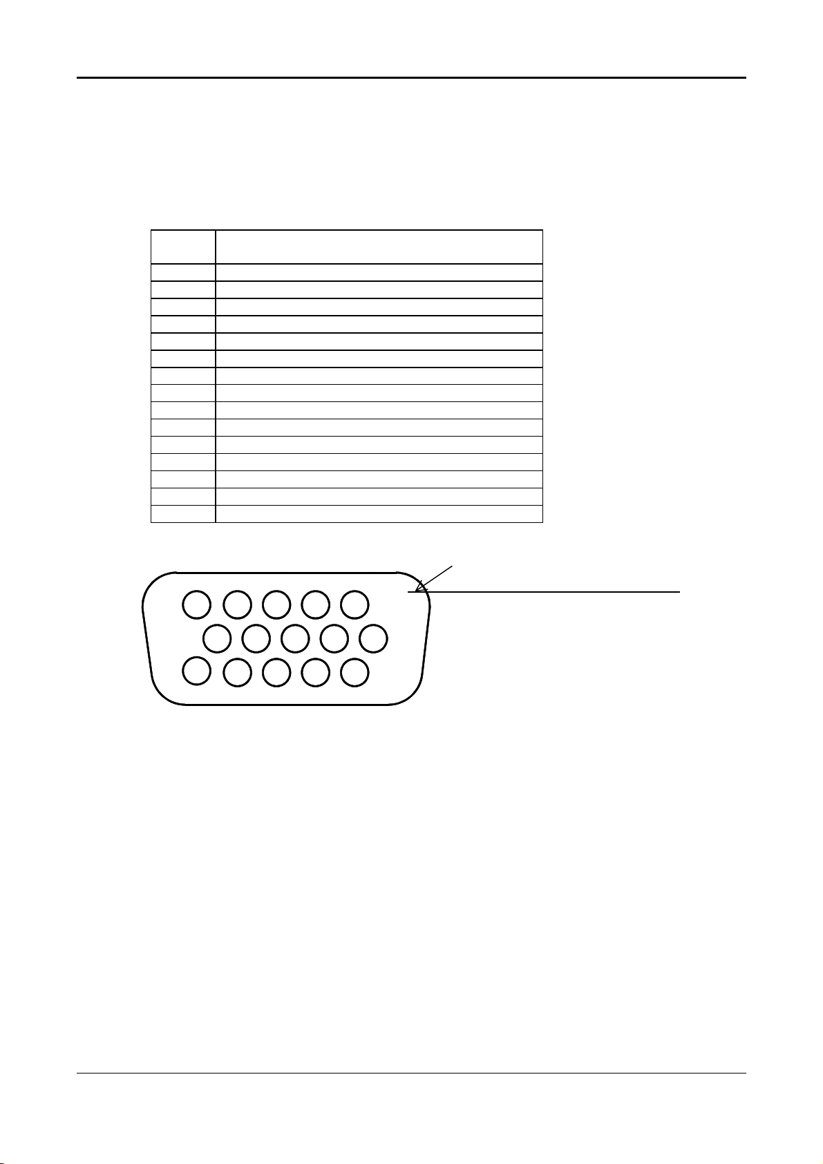
2.4.5 Video Input Connector
Analog Video Input Connector: 15pins mini D-Sub
Table 2.4.5. Pin Assignment for D-sub Connector
PIN
NO.
1 RED VIDEO
2 GREEN VIDEO
3 BLUE VIDEO
4 GROUND
5 GROUND
6 RED GROUND
7 GREEN GROUND
8 BLUE GROUND
9 PC5V (+5V DDC)
10 CABLE DETECTION
11 GROUND
12 SDA
13 H.SYNC
14 V.SYNC
15 SCL
Separate Sync
Colour of Plastic Parts: Blue (PC99)
5 1
10
15
D-sub Connector
6
11
10
Page 13
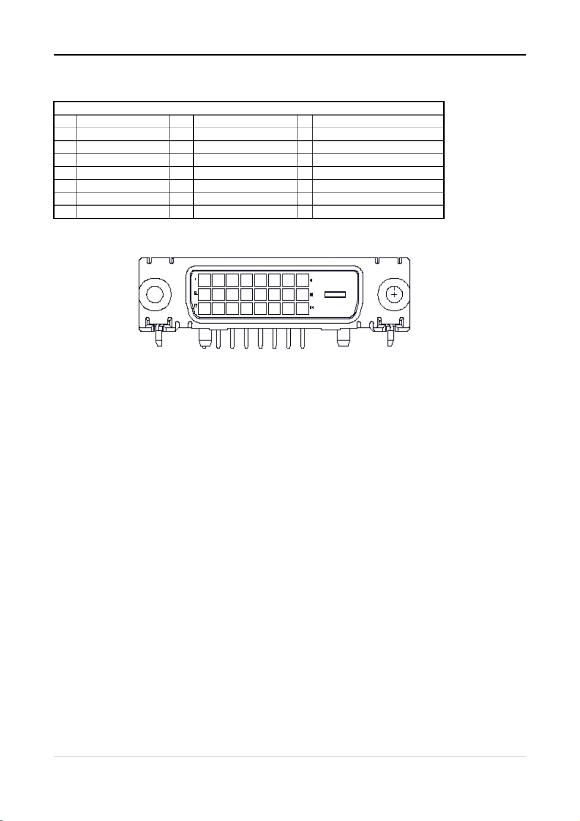
Digital Video Input Connector: DVI-D (T.B.D)
Table 4-3-3. Pin Assignment for DVI-D (24pin) Connector
Pin – Assignment of DVI –D Connector :
1 TX2- 9 TX1- 17 TX0-
2 TX2+ 10 TX1+ 18 TX0+
3 Shield (TX2 / TX4) 11 Shield (TX1 / TX3) 19 Shield (TX0 / TX5)
4 NC 12 NC 20 NC
5 NC 13 NC 21 NC
6 DDC-Serial Clock 14 +5V power *) 22 Shield (TXC)
7 DDC-Serial Data 15 Ground (+5V) 23 TXC+
8 No Connect 16 Hot plug detect 24 TXC-
*) In case, the power of the PC unit is switched off and the power of the monitor is switched on,
no voltage may occur at pin 14.
11
Page 14
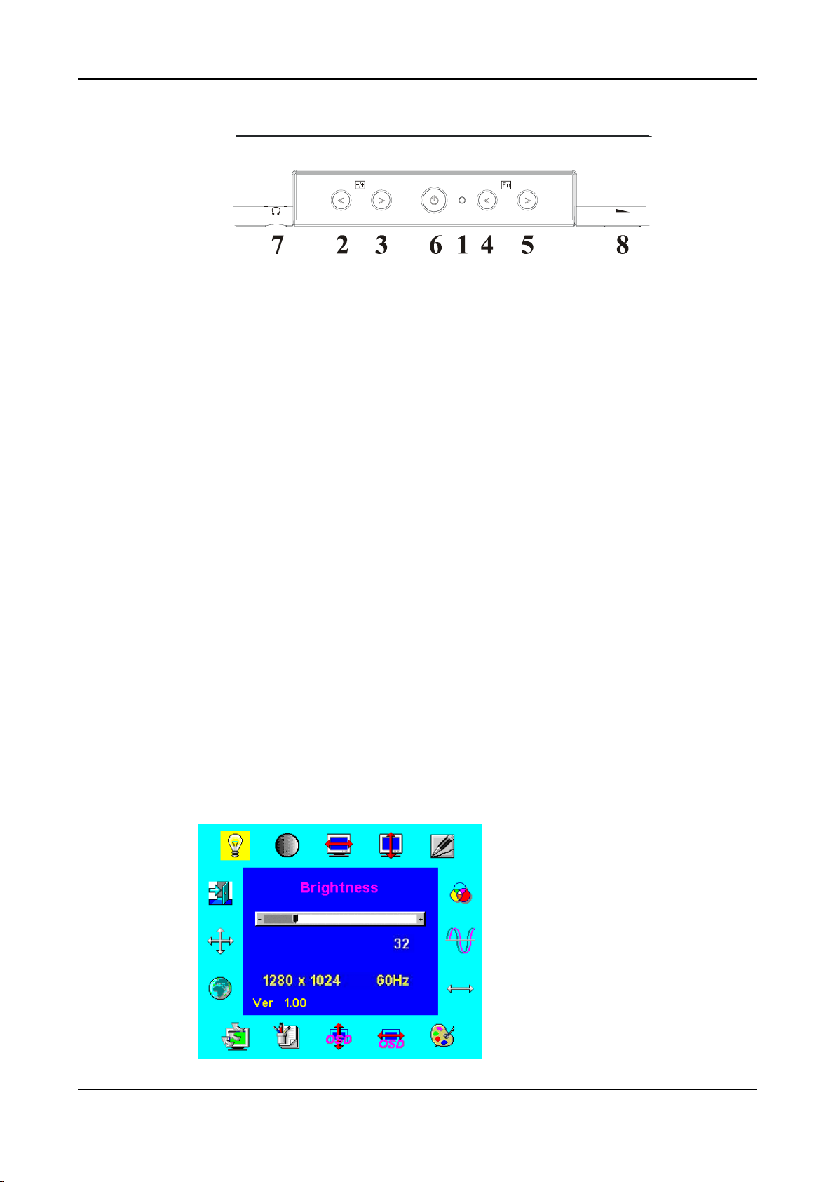
2.5 CONTROLS
2.5.1 Control Panel (Monitor Front Panel)
1. Power LED, will be green when monitor is on; be amber when in power saving mode.
2. Adjust decrease.
3. Adjust increase.
4. Function select anti-clockwise.
5. Function select clockwise.
6. Power ON/OFF switch, push to ON and push to OFF. (toggle switch)
7. Ear phone jack. (for CML175SXW2/2B only)
8. Volume Control. (for CML175SXW2/2B only)
Note: When OSD Menu is off, press button 2 and 3 at the same time can activate “Auto
Adjustment” immediately.
2.5.2 OSD Functions
• OSD Format: Refer to following figure.
• OSD Border: Cyan colour
• OSD Tunable Item: The 16 icons that around the border.
• Selected Item: Yellow background
• Comment: Magenta foreground, Blue background
page format :
12
Page 15

Description:
• Brightness: Brightness adjustment, the range from 0 to 100. Default = 100
• Contrast: Contrast adjustment, the range from 0 to 100. Default = 50
• H. Position: Horizontal position adjustment.
• V. Position: Vertical position adjustment.
• Phase: Focus adjustment, the range from 0 to 255 steps.
• OSD position: OSD position adjustment.
• Auto Adjustment: This feature will automatically adjust size, position, clock and phase.
It takes 3-5 seconds to finish. When auto start, it shows “Auto
Adjusting….” message.
• Clock: Frequency tracking adjustment. The max range from -50 to +50, but
some modes the range will be limited.
• Graph Text: 640x400 (GRAPH) or 720x400 (TEXT) mode select.
• Language: 5 kinds of language for description, including (English, German,
French, Spanish, Italian)
• Recall: Recall the default value.
• Colour Temp: Colour temperature for standard 9300°, 6500°, 7500° or user defined.
User:
User R: Red signal gain by user defined.
User G: Green signal gain by user defined.
User B: Blue signal gain by user defined.
7500°: Set CIE coordinate at 7500°K colour temperature.
6500°: Set CIE coordinate at 6500°K colour temperature.
9300°: Set CIE coordinate at 9300°K colour temperature.
• Exit: Exit OSD menu function.
Sharpness : Adjust the scale-up effect (smoother or sharper.)
OSD Transparency: Adjust the transparency level of OSD. The range is from 0 to 100 scales.
Comment:
• 1280x1024: Current mode resolution.
• 60 HZ: Current mode vertical frequency ±1Hz.
• VER 1.00: Firmware revision.
13
Page 16
Other Features:
Intellectual-Auto unit can start the Auto-Adjustment automatically when input a new
display mode at first time. After the adjustment, the unit will remember this mode and
switch to optimised condition automatically for this mode whenever encounter this mode
again. Total 27 recent used modes are recorded into the unit.
VESA DPMS Functionality When signaled by the host CPU, the unit shows a black
screen about 3 seconds. If no further signal, then it shows “No Signal” and enter power
saving mode.
2.6 White Colour Temperature
White colour temperature is 4 preset as 9300, 7500, 6500 and User,
Default value of user colour should be user which is maximum setting for panel.
Target of colour setting
Colour
Temp.
9300K 0.281 0.297 +0.03 0.189 0.446 u’v’ < 0.01*
7500K 0.299 0.315 +0.03 0.194 0.459 u’v’ < 0.01*
6500K 0.313 0.329 +0.03 0.198 0.469
User - - - - -
User should follow “Microsoft Windows Colour Quality Specification for Liquid Crystal Display OEMs”.
(http://www.microsoft.com/hwdev/tech/color/ColorTest.asp)
Colour Co-ordinate Tolerance Colour Co-ordinate Tolerance
x y u’ v’
*) TCO’0X A.2.6.1 requirement
u’v’ <
0.01*
14
Page 17
2.7 POWER SUPPLY
2.7.1 Input Voltage Range
The monitor shall operate within specification over the range of 90 to 265VAC power supply.
2.7.2 Input Frequency Range
Input power frequency range shall be from 47.5 to 63Hz over the specified input
voltage range.
2.7.3 Quick Specification Review
• Input Current
1.2A (max) at 90VAC input and full load
0.6A (max) at 264VAC input and full load.
• Inrush Current @ cold start
30A(0-peak) @ 110Vac, 50A (0-peak) @ 220Vac
(measured when switched off for at least 10 mins.)
• Output
Tolerance Output Current
Output Volt - MIN MAX
+5Vdc ±5% 0A 1.0A
+5Vdc ±5% 0A 1.5A 4.8~5.2V dc
+12Vdc +25%/-5% 0A 2.2A 11.4~15Vdc
• Total Output Power: 48 Watt max.
• Withstanding Voltage: 1.5Kvac or 2.2KVdc for 1 minute.
• Leakage Current: < 0.25mA/100Vac, <3.5mA/230Vac
• Efficiency: 70% min. @15V/230VAC, maximum load.
2.7.4 Power Management
2.7.4.1 Meets VESA DPMS Proposal
The monitor must comply with the Microsoft On Now specification, with a minimum of three power
management states, as defined by the VESA DPMS document. The front panel of the monitor must
appropriately display the DPMS state, For example:
Volt Tolerance
4.8~5.2Vdc
(for Audio)
DPMS ON : The power LED is Green
DPMS OFF : The power LED is Amber
2.7.5 Power Consumption
On mode 48 Wmax Green
Off mode 4 Wmax Amber
DC power off 4 Wmax Dark
Power SW off 1 Wmax Dark
Disconnection 4 Wmax
15
Dark (DC power off)
Amber (DC power on)
Page 18

Power saving states are measured with speakers attached but not worked.
The recovery time from stand by /suspend/off mode to on mode is 3 seconds maximun.
2.7.6 Power Connector
All units shall have an IEC/CEE-22 type male power receptacle.
2.8 Plug & Play (EDID)
The monitor will be capable of sending a VESA standardised EDID file through the DDC (pins 12,
15 of the VGA connector).
2.9 Audio Technical Specification (for CML175SXW2/2B only)
2.9.1 General Description:
Output power : 1W + 1W maximum
Total harmonic distortion : Less than 1 % (except speakers distortion)
Input signal sensitivity : 0.5 Vrms for full output
Input impedance : 47 Kohm +/- 5 %
Frequency response range : 100Hz – 20kHz (except speakers response)
Difference of L and R output : Less than 2 dB
°°°°
2.9.2 Electrical Characteristics (Tamb=25
)
Audio Amplifier (USE Panasonic VP-7723A Audio Analyzor)
Item Audio Input Freq.
Spec.
Comment
Min. Typ. Max.
Input Voltage(V) - 5 -
Input Current(m A) - 500 800
Audio Voltage Gain 500m Vrms 1KHz - - 6 d B Volume Max.,load 4 Ω
Frequency Response 500m Vrms 300Hz-20KHz -10dB - +10d B Volume Max.,load 4 Ω
Signal to Noise ratio 500m Vrms 1KHz - - -40dB Volume Max.,load 4 Ω
Total harmonic distortion 500m Vrms 1KHz 1% except speakers distortion
Cross talk 500m Vrms 1KHz - - -30dB Volume Max.,load 4 Ω
Output Watt. 500m Vrms 1KHz - - 1W Volume Max.,load 4 Ω
Volume Control - - - Analog
2.9.3 Speakers
Maximum Power : 1 W per speaker(max)
Impedance : 4 ohm +/- 15 % @ 1KHz 1.0Hz
Frequency response range : 300 Hz – 20 kHz (SPL – 10 dB)
Total harmonic distortion : Less than 5% @ 0.125W 1KHz
2.9.4 Headphone Output
Output Power : 1.6 mW for 32 ohms Headphone
16
Page 19

3. VL-713 DISPLAY CONTROL BOARD
3.1 Description
The VL-713 display control board is designed to directly receive RGB Analog and TMDS
DVI signal to optimum LCD timing signals so as to construct a high display quality LCD
monitor.
3.2 Features
•
Support for image expansion and reduction.
• On board micro-processor to detect display timings and control user functions.
• Uses Genesis design to generate optimum LCD timings.
• Uses EEPROM to memorise every adjusted parameter.
• Supports up to 25 display modes from VGA to SXGA.
• Supports up to 5 display modes from VGA to SXGA by TMDS.
• Offers full screen expansion function on non-XGA mode (automatic).
• Supports OSD functions.
• Supports VESA DPMS function.
• Supports DDC1/2B functions.
• Supports English and Japanese language for OSD description.
• The longest time for mode change is 3 seconds.
17
Page 20

3.3 BLOCK DIAGRAM
System Block Diagram
3.4 Connector Locations
18
Page 21

3.5 Connector Type
Location Type Maker Number of pins
CN1 DVI-D FEMALE 24
CN4 96113-0803 E&T 8
CN6 4501-10 E&T 10
CN5 98210-4011 E&T 40
CN302 98115-0313 E&T 3
CN301 4300-11P E&T 11
CN2 D-SUB E&T 15
3.6 Connector Pin Assignment
3.6.1 CN1
Pin # Signal Name Description Pin # Signal Name Description
1 RX2-
2 RX2+
3 RX2 SHILD
4 NC do not connect 19 RX0
5 NC do not connect 20 NC do not connect
6 DDC/SCL DDC2B clock 21 NC do not connect
7 DDC/SDA DDC2B data 22 RXC SHILD Shield for TMDS clock
8 Analog Vs Analog V-sync 23 RXC-
9 RX1-
10 RX1+
TMDS negative
differential
TMDS positive
differential output,
channel 2
Shield for TMDS
channel 2
TMDS negative
differential output,
channel 1
TMDS positive
differential output,
channel 1
16 HTPLG +5V Supply
17 RXO-
18 RXO+
24 RXC+
TMDS negative
differential output,
channel 0
TMDS positive
differential output,
channel 0
shield for TMDS
channel 0
TMDS negative
differential output,
reference clock
TMDS positive
differential output,
reference clock
11 RX1 SHILD
12 NC do not connect
13 NC do not connect
14 DOC +5VDC DDC2B logic +5V
15 DDC GND DDC2B logic GND
Shield for TMDS
channel 1
19
Page 22

3.6.2 CN5
PIN No. Symbol Function
38 VDD
39 VDD
40 VDD
35 NC No Connection
36 NC No Connection
37 NC No Connection
1,2,3 GND Power Ground
17 RXE3+ Positive Transmission Data of Pixel 3 (EVEN data)
16 RXE3- Negative Transmission Data of Pixel 3 (EVEN data)
14 RXEC+ Positive Sampling Clock (EVEN data)
13 RXEC- Negative Sampling Clock (EVEN data)
11 RXE2+ Positive Transmission Data of Pixel 2 (EVEN data)
10 RXE2- Negative Transmission Data of Pixel 2 (EVEN data)
6,9,12 GND Power Ground
8 RXE1+ Positive Transmission Data of Pixel 1 (EVEN data)
7 RXE1- Negative Transmission Data of Pixel 1 (EVEN data)
15,18,21,24 GND Power Ground
5 RXE0+ Positive Transmission Data of Pixel 0 (EVEN data)
4 RXE0- Negative Transmission Data of Pixel 0 (EVEN data)
32 RXO3+ Positive Transmission Data of Pixel 3 (ODD data)
31 RXO3- Negative Transmission Data of Pixel 3 (ODD data)
29 RXOC+ Positive Sampling Clock (ODD data)
28 RXOC- Negative Sampling Clock (ODD data)
30,33,34,27 GND Power Ground
26 RXO2+ Positive Transmission Data of Pixel 2 (ODD data)
25 RXO2- Negative Transmission Data of Pixel 2 (ODD data)
23 RXO1+ Positive Transmission Data of Pixel 1 (ODD data)
22 RXO1- Negative Transmission Data of Pixel 1 (ODD data)
20 RXO0+ Positive Transmission Data of Pixel 0 (ODD data)
19 RXO0- Negative Transmission Data of Pixel 0 (ODD data)
Power Supply : +5V
3.6.3 CN302
Pin No. Signal Comment
1 Audio-RIN Audio Right Input
2 GND
3 Audio-LIN Audio Left Input
20
Page 23

3.6.4 CN301
Pin No. Signal Comment
1 +5 VDD
2 VR
3 L+
4 L-
5 AGND
6 HP-S
7 HP-L
8 HP-R
9 AGND
10 R+
11 R-
Audio +5V
Audio Volume Control
Audio Left+ Output
Audio Left- Output
Analog GND
HP-Sense
Audio Left Output (Head Phone)
Audio Right Output (Head Phone)
Analog GND
Audio Right+ Output
Audio Right- Output
3.6.5 CN6
Pin NO. Signal Comment
1 +5 V Audio Power
2 GND Audio GND
3 GND GND
4 GND GND
5 BRIGHT Brightness Adjustment
6 PS Power Saving
7 PBIAS Back Light ON/OFF
8 +5VB From USB power
9,10 +5V From main power
3.6.6 CN4
Pin NO. Signal Comment
1 LED-Y Power saving mode
2 LED-G Monitor is ON
3 GND GND
4 KEY-ON/OFF KEY- ON/OFF
5 KEY−UP KEY-Brightness Increase
6 KEY-DOWN KEY-Brightness Decrease
7 KEY-RIGHT KEY-Volume Increase
8 KEY-LEFT KEY-Volume Decrease
21
Page 24

4. VK-713 Control Panel Board
4.1 Description
The VK-713 is designed to offer a user interfaced control panel which passes and receives
signals to and from VK-713 display control board.
4.2 Connector and Switch Locations
4.3 Connector Type
Location Type Maker Number of Pins
J4 4301-08 E&T 8
J2 4301-11 E&T 11
J1 87502-0200 ACER 2
J3 87502-0200 ACER 2
JP1 SCJ-0348-C SC 9
4.4 Connector Pin Assignment
4.4.1 J4
Pin NO. Signal Comment
1 KEY-LEFT Function select anti-clockwise key
2 KEY-RIGHT Function select anti-clockwise key
3 KEY-DOWN Adjust down key
4 KEY-UP Adjust up key
5 KEY-POWER Power ON/OFF key
6 GND GND
7 LED-G Power is ON
8 LED-Y Power is OFF
4.4.2 J2
Pin NO. Signal Comment
1 +5 VDD Volume Control
2 Volume Volume Control
3 L OUT+ Audio Output L+
4 L OUT- Audio Output L-
5 AGND Audio GND
6 HP-S Audio Earphone sensor
7 HP-L Audio Earphone Output L
8 HP-R Audio Earphone Output R
9 AGND Audio GND
10 R OUT- Audio Output R+
11 R OUT+ Audio Output R-
22
Page 25

4.4.3 J3
Pin NO. Signal Comment
1 L+ OUT Audio Output L+
2 L- OUT Audio Output L-
4.4.4 J1
Pin NO. Signal Comment
1 R+ OUT Audio Output R+
2 R-OUT Audio Output R-
4.5 Switch Definition
Location Definition
S1 Power ON/OFF
S4 Function select in clockwise direction
S5 Function select in anti-clockwise direction
S2 Adjust up
S3 Adjust down
4.6 LED Definition
Location Definition
D1 Green for ON mode; Yellow for OFF mode; yellow for Power Saving mode; Dark for DC
power OFF mode.
23
Page 26

5. POWER SUPPLY & INVERTER BOARD
5.1 Description
The Power supply and Inverter board is designed for the display control board and the
lighting up of the back-lights of LCD module.
5.2 Power Supply ( AC to DC section)
5.2.1 Input Voltage Range
The monitor shall operate within specification over the range of 90 to 265VAC power supply.
5.2.2 Input Frequency Range
Input power frequency range shall be from 47.5 to 63Hz over the specified input
voltage range.
5.2.3 Quick Specification Review
• Input Current
1.2A (max) at 90VAC input and full load
0.6A (max) at 264 VAC input and full load.
• Inrush Current @ cold start
30A (0-peak) @ 110VAC, 50A (0-peak) @ 220VAC
(measured when switched off for at least 10 mins.)
• Output
Tolerance Output Current
Output Volt - MIN MAX
+5Vdc ±5% 0A 1.0A
+5Vdc ±5% 0A 1.5A 4.8~5.2V dc
+12Vdc +25%/-5% 0A 2.2A 11.4~15Vdc
• Total output power: 48Watt max.
• Withstanding voltage: 1.5KVAC or 2.2KVDC for 1 minute.
• Leakage current: < 0.25mA/100VAC, <3.5mA/230VAC
• Efficiency: 70% min. @ 115V/230VAC, maximum load.
Volt Tolerance
4.8~5.2Vdc
(for Audio)
24
Page 27

5.3 Inverter (DC to AC Section)
5.4 Electrical Characteristics
5.4.1 For Hydis PANEL (HT17E12-200)
MIN. TYP. MAX. COMMENT
INPUT VOLTAGE 11.4V 12.0V 15V 12V+25%/-5%
INPUT CURRENT -------- 2A --------
Normal BACKLIGHT
VOLTAGE
LAMP CURRENT
DRIVING
FREQUENCY
EFFICIENCY -------- 75% --------
Vin ON/OFF sequence -------- 0.5S --------
OLP TIME -------- 1S _
BRIGHTNESS
RANGE
Brightness control 0.4V _ 3.3V
Brightness _ 250cd/m
Strike voltage at 0°C 1310 Vrms _ _
-------- 705V rms. --------
3mA rms. 6.5mA rms 7 mA rms
40KHz -------- 60KHz
30% -------- 100%
2
_
Vin=12V,
Vbrite=3.3V
Vin = 12V,max
brightness
Open lamp
protection time
3.3V, brightness
max.
Operating life time 40,000 hrs 50,000 hrs _ (note)
Note:
Life time (hr) can be defined as the time in which it continues to operate under the condition:
Ta=25±2°C, IL =6.5mArms until one of the following event occurs:
1. When the brightness becomes 50%
2. When the startup voltage (Vs) at 0°C becomes higher than the maximal value of Vs specified above.
25
Page 28

5.5 Connector Locations
5.5.1 Connector Type
JM778-
Location Type Maker Number of Pins
J940, J980, SM02 (2.0) B-BHS-1-TB JST 2
J941, J981
P803 96113-1203 E&T 10P
P801 SA-4S-066 Huajie 3
P60 SCJ03451X9 SC 3
P62 98115-0313 E&T 3
5.5.2 Connector Pin Assignment
5.5.2.1 J940, J980, J941, J981
Pin NO. Signal Comment
1 HV High voltage for lamp
2 LV Low voltage for lamp
26
Page 29

5.5.2.2 P803 For Display Control Board (Interface)
Pin NO. Signal Comment
1 +5Vaudio +5Vdc for Audio Circuit
2 GND/Audio Ground for Audio Circuit
3,4 GND Common Ground
5 BRITE Brightness adjustable range:
0.4V<min>~3.3V<max>
6 NC
7 Enable Backlight ON/OFF control (Active High)
ON:1.5~5.5V OFF:-0.3~1.0V.
8,9,10 Vcc +5Vdc supply to Interface BD, always on.
27
Page 30

6. TROUBLESHOOTING
6.1 Main Procedure
28
Page 31

6.1.1 Power Circuit and Backlights Troubleshooting
29
Page 32

6.1.2 Performance Troubleshooting
30
Page 33

6.1.3 Function Troubleshooting
31
Page 34

7. MECHANICAL REQUIREMENTS
7.1 Vibration and Shock
All testing shall be done in each of three mutually perpendicular axes referenced to the
position of the system as it is in front of the user (i.e. front-to back, side-to-side and top-tobottom).
7.1.1 Non-Operating
The unit should suffer minimal visible cosmetic damage or damage that presents a safety
hazard or impairs the setup and operation of the system after testing.
Sinusoidal Vibration: 0.75G zero-to-peak, 10 to 500Hz, 0.5 octave / minute sweep rate.
This requires one sweep, 10 to 500 to 10Hz, along each of the three axes.
Random Vibration: 0.008G
hour for each of the three axes.
Half Sine Wave Shock: 120G peak, half sine pulse, 2ms pulse duration. Testing shall
consist of one shock in each direction in each axis, for a total of 6 shock inputs.
Square Wave Shock: 40G peak acceleration, 160 inches / second velocity change. There
shall be one shock in each direction in each axis, for a total of 6 shock inputs.
2
/Hz, 10 to 500 Hz, nominal 2GRMS. The test shall be for one
7.2 Package Drop Specification
Listed below are standards of drop heights for monitor product
Product Weight Height Specs
<9.1 Kg 0.76 m
9.2~18.2 Kg 0.66 m
18.3~27.2 Kg 0.61 m
27.3~45.4 Kg 0.46 m
7.2.1 Drop Test Sequence
Drop Order Drop Point Drop Times
1 Right Front Bottom Corner 1
2 Right Bottom Edge 1
3 Right Front Edge 1
4 Front Bottom Edge 1
5 Bottom Side 1
6 Top Side 1
7 Front Side 1
8 Back Side 1
9 Left Side 1
10 Right Side 1
32
Page 35

7.3 Dimension Size and Weight
Dimension size 374 (W) x 394.5 (H) x 204 (D)
Net Weight 5Kg
Gross Weight 7Kg
7.4 Gap Spec.
7.4.1 The step between front bezel and back cover shall be within specification.
Top Left and Right
Back cover concavity Back cover concavity
0 mm ≤ X ≤ 0.8 mm 0 mm ≤ X ≤ 0.8 mm
JM777 / JM778 JM777 / JM778
LCD Horizontally
The angle between front bezel and LCD unit in bottom side should not large than 1.0mm.
JM777 JM778
33
Page 36

The angle between from bezel and LCD unit in bottom side should not large than 4.0mm
JM777 JM778
7.5 Tilt Base Rotation
Tilt up 30 ± 1°/ down 5 ±1°
7.6 Swivel Base Rotation
Swivel Right 45 ±1° / Left 45 ±1°
7.7 Plastic Material
Front Bezel ABS 94V-0
Back Cover ABS 94V-0
The Others ABS 94HB
TCO’99 (Optional)
Front Bezel PC + ABS 94 – 5V
BACK COVER PC + ABS 94 – 5V
The others ABS 94 HB
7.8 GAP Spec.
Gap between panel with bezel is 0 mm < gap < 1.5 mm
34
Page 37

8. Power Line Transient Test (IEC 61000-4-4 Fast
Transients/Burst)
TEST CONDITIONS & PROCEDURE: (Follow IEC 61000-4-4)
Test Condition :
The condition is base on operating with 50Ω load.
8.1 Peak Voltage:
2 KV (applies the Level 3 typical Industrial Environment” of IEC 61000-4-4)
8.2 Polarity : + / -
8.3 Repetition Frequency of the impulse: 5 KHz.
±±±±
8.4 Rise-Time: 5ns
8.5 Impulse Duration: 50 nS
8.6 Relation to Power Supply: Asynchronous
30%
±±±±
30%
8.7 Burst Duration: 15 ms
8.8 Burst Period: 300 ms
8.9 Climatic Conditions:
- Ambient Temperature: 15°C to 35°C
- Relative Humidity: 45% to 75%
- Atmospheric Pressure: 86KPa to 106KPa
8.10 Test Procedure:
The monitor Display set high-resolution mode, AC input is AC 240V.
Note :
8.10.1
IEC 61000-4-4 defines that power supply, I/O line and control line all shall perform the
transient test. The I/O line and control line is applied with only half of peak voltage (1
KV).
8.10.2
For the comparison of wave-shape generated by different generator, so the test must uses a
scope with at least 400 MHz bandwidth, and coupled to 50Ω to monitor the rise-time,
impulse, duration and repetition rate of the impulses within one burst.
±±±±
20%
±±±±
20%
35
Page 38

WAVESHAPE
36
Page 39

9. Power Line Surge Test (IEC 61000-4-5 Surge)
9.1 Climatic Condition
The climatic conditions shall be within the following ranges:
9.1.1 Ambient Temperature: 15
9.1.2 Relative Humidity: 10% to 75%
9.1.3 Atmospheric Pressure 86kPa (860 mbar) to 106kPa (1060mbar)
Note: The temperature and relative humidity should be recorded in the test report.
°°°°
C to 35
°°°°
C
9.2 Test Conditions:
9.2.1 Wave-shape of the current surge: (refer to IEC 61000-4-5)
Open circuit voltage: (1.2 / 50 µs)
Short circuit current: (8 / 20 µs)
9.2.2 Polarity: positive / negative
9.2.3 Phase Shifting: in a range between 0º to 270º versus the AC line phase angle
9.2.4 Repetition Rate: at least 1 per minute
9.2.5 Number of Tests: at least 5 positive and 5 negative at the selected points.
9.3
The surge will be applied between lines and between lines and ground.
9.4
If not otherwise specified, the surge to power supply circuits shall be applied synchronised to
the voltage phase at the zero crossing and the peak value of the AC voltage wave. (Positive
and negative)
9.5
The surge voltage for test is from 1KV and increases 1KV for each step.
9.6
The recommended severity levels for the surge voltage test is 2.0KV and without any
degradation or loss of function that is not recoverable due to damage of component or
software allowed.
9.7 Display set high-resolution mode, AC input is AC 240V.
37
Page 40

10. ENVIROMENT REQUIREMENT
10.1 Operating
Temperature 5°C ~ 40°C
Relative Humidity 20% to 80%
Altitude Sea level to 8000ft
10.2 Storage or Shipment
Temperature -20°C ~ +60°C
Relative Humidity 5% to 85%
Altitude Sea level to 40,000ft
10.2.1 TEST PROCEDURE:
• Put in temperature chamber under 60°C Time: 24 hours
• Back to room temperature Time: 4 hours
• Put in temperature chamber under -20°C Time: 24 hours
• Back to room temperature Time: 4 hours
• Repeat the process 2 times.
38
Page 41

11. REGULATION COMPLIANCE
11.1 This product complies with the most current revisions of following
regulations:
UL/CUL
{UL 1950/ CSA C22.2 NO950}
EN 60950/CB Scheme Safety of Information Technology Equipment including Electrical
MPR 1990:8 Test methods for visual display units.
MPR 1990:10 User handbook for evaluation visual display units.
ISO 9241-3: Ergonomic requirements for office work with visual display terminals
ISO 9241-7: Ergonomic requirements for office work with visual display terminals
ISO 9241-8: Ergonomic requirements for office work with visual display terminals
NUTEK/EPA Requirements of power saving according to NUTEK Spec.
TCO 1999 (option) Requirements for Environmental Labeling of Personal Computers.
TUV/GS Safety regulation for displays work places in the office sector.
FCC 47 CFR, Chapter 1,
Subchapter A, Part 15, Subpart B
Standard for Safety of Information Technology Equipment including
Electrical Business Equipment
Business Equipment
(VDTs)-Visual display requirements.
(VDTs)-Requirements for display with reflections.
(VDTs)-Requirements for displayed colours.
803299/94/96, EPA Energy star.
Test methods for Ergonomic, Emission, Energy Efficiency, safety.
A digital device that is marketed for use in a residential environment
not withstanding use in commercial, business and industrial
environments.
CISPR 22 Limits and methods of measurements of radio interference
characteristics of information technology equipment.
CE LVD Directive (73/23/EEC) Safety: EN60950
CE EMC Directive (89/336/EEC)
IEC 61000-4
VCCI (option) Specification for limits and methods of measurement of radio
BSMI (option)
EMI: EN55022 class B
Harmonics: EN61000-3-2
Voltage Fluctuation/Flicker: EN61000-3-3
Immunity: EN55024
IEC 61000-4-2 Electrostatic Discharge
IEC 61000-4-3 Radiated Electromagnetic Field
IEC 61000-4-4 Fast Transients/Burst
IEC 61000-4-5 Surge
IEC 61000-4-6 Conducted Disturbance, Induced by Radio
Frequency Fields
IEC 61000-4-8 Power Frequency Magnetic Field
IEC 61000-4-11 Voltage DIP/Interruption
interference characteristics of information technology equipment.
Class B conformity verification report from the VCCI
CNS 13438, Class B
39
Page 42

11.2 Electrostatics Discharge (ESD)
E.S.D Test
This test follows IEC 61000-4-2
Discharge Voltage Level :
Criteria Contact Discharge (KV) Air Discharge (KV)
Class C ±4 ±4
Class B ±6 ±8
Class A ±8 ±15
Class A : Temporary degradation or loss of function or performance which requires
operator Intervention or system reset.
Class B : Temporary degradation or loss of function or performance which is self-
recoverable
Class C : Normal performance within the specification limits
Discharge times: 20 times for each discharge point, time interval 1 second.
In the case of acceptance tests, the test program and the interpretation of the test results are
subject to agreement between manufacturer and user.
The test documentation shall include the test conditions and the test results.
40
Page 43

Ambient temperature : 15 to 35°C
Relative humidity : 30 to 60%
12. QUALITY AND RELIABILITY
12.1 Quality Assurance
Unless otherwise specified in this specification or the applicable purchase order, the supplier shall
be responsible for maintaining a statistical process program or performing inspections that are
sufficient to assure that the parts supplied meet the requirements specified herein.
12.2 Reliability
The product shall have a designed MTBF of greater than 20,000 hours during its useful life.
41
Page 44

APPENDIX A
POWER SUPPLY AND INVERTER BOARD DIAGRAMS
CML174SXW2
CML175SXW2
42
Page 45

HU AJIE
SA- 4S-066
P801
L
N
FG
1
2
3
F801
T3.15A/250V
C803
102 Y1
C804
102 Y1
L801
CL900007400
3
1
0.33uf X2
4
2
C801
C803A
RT801
SCK085
222 Y1
J801
P802
SW
R801
510K / 1206
R802
510K / 1206
MAIN
POWER
L802
CL900007400
3
1
VA801
ZV07D511
R813
27K/0603
5
RT
2
FB
0.33uf X2
4
2
3
VINGND
U801
SG6841/SOP8
1
C802
EN
5V
3
2
1
R911
100K/0603
P803
10
HEADER 10
R912
100K/0603
2
Q901
2N7002
C930
470uF/25V
ZD922
HZ6.2B
C924
473/0603
ZD962
HZ6.2B
F901
KE40
JP1
3
Q902
2N7002
1
+
C963
473/0603
JP2
R922
10K/0603
R914
47K/ 0603
C902
103/0603
R962
10K/0603
C903
1U/0805
RT
103/X7R/0603
R915
51K/0603
R917
12K/0603
D980
U920
FDS4435
1
S
2
S
3
S
4 5
G D
D981
SB140
1
S
2
S
3
S
4 5
G D
U950
FDS4410
U930
FDS4435
1
S
2
S
3
S
4 5
G D
D983
SB140
1
S
2
S
3
S
4 5
G D
U960
FDS4410
+
C907
D982
SB140
R903
22/ 0603
C904
0.47U/ 0603
+
R913
560K/1%/0603C818
SB140
8
D
7
D
6
D
8
D
7
D
6
D
8
D
7
D
6
D
8
D
7
D
6
D
R901
27K/1%/0603
+
C905
1U/0805
C906
104Z/0603
C908
222/X7R/0603
C922
4.7U/ X7R/1206
C923
4.7U/X7R/1206
U901
OZ960G/SOP20
1
CTIMR
2
OVP
3
ENA
4
SST
5
VDDA
6
GNDA
7
REF
9
FB
10
CMP
6,7
2,3
104/0603
OZ960
47K/1%/0603
R905
T901 EEA-17
37 :2100
R916
1M/0603
C914
T902 EEA-17
6,7
2,3
37 :2100
80.6K/1%/0603
NDRV_B
PDRV_A
CT
RT
PWRGND
LCT
DIM
LPWMRT1
PDRV_C
NDRV_D
1N4148/0603
5
4
8
1
D931
BAV99
2
1
D932
BAV99
2
1
5
4
8
1
D933
BAV99
2
1
D934
BAV99
2
1
R902
20
19
18
17
16
15
14
138
12
11
D906
C980
12p/ 3KV
183/0603
183/0603
3
C981
C981A
183/0603
C983
12p 3KV
3
C984
3
3
INVERTER
C912 220P/ NPO/0805
RT
R906 62K/1%/0603
C911 103/X7R/0603
C910 104/0603
R907 100K/1%/0603
+
C909
4.7U/10v
D941
BAV99
3
3
D942
BAV99
C971
47p/ 3KV
C972
47p/ 3KV
R970
453/1%/0603
C982
222/0603
C980A
12p/ 3KV
C982A
222 /0603
47p/ 3KV
47p/ 3KV
C985
222/0603
R971
453/ 1%/0603
C983A
12p 3KV
C984A
183/0603
R972
5.1K/0603
1
2
1
2
3
C973
BAV99
C974
R945
5.1K/0603
D945
3
BAV99
D946
BAV99
D947
C985A
222 /0603
D943
BAV99
D944
BAV99
R940
5.1K/0603
1
2
D948
BAV99
R946
453 1%/0603
J940
ACES 87210-0236
2
1
2
1
ACES 87210-0236
453/1%/0603
R973
5.1K/0603
1
2
R947
ACES 87210-0236
2
1
2
1
ACES 87210-0236
2
HV
1
LV
3
2
HV
1
LV
3
J980
J941
2
HV
1
LV
3
2
HV
1
LV
3
J981
Q841
BT151
C862
104/0603
+
R954
510/ 1206
ZD952
RLZ5.6
R956
5.1K/ 0603
123456789
GND/Audio
Common Ground
+5 V Audio
D987
NC/0603
1
2
Q950
3
2N3906
Q952
2N3904
3
2
1
ZD901
HZ8.2B
104/0603
BRI. ADJ
R987
NC/ 0603
C952
100 1/2W FUSE
K
A
12
3
2
103 /0603
8
7
R846
150/0603
1
1
U802
KA431Z
C60
R841
R850
47/0603
R
R800
0.2/ 1W FUSE
3
C810
103Z
R820
2/1206
P6KE200A
+
C805
100uf/400V
R807
15/ 1/2W
TVS1
R820A
2/1206
100k/2W
PS1010R
D802
PS104R
Q801
2SK2645
R819A
2/1206
R806
L803
Bead
1
R819
2/1206
2
3
+
-
4
C809
10uf/50v
BD801
2KBP08M
R822
820K/1206
R804
27K/0603
1
+
2
R821
680K/1206
7
VDD
8
GATE
4
RI
SENSE
6
C806
222/1KV
LTV-817M-B
T801
EE-30
5
3
4 9,10,11
6
1,2
C800
222 Y1
103/1KV
U800
4
3 2
102/1KV
D841
ER1002F
D842
SB560
R842
10 1/2W FUSE
C842
103Z
D843
ER302
3.65K/1%/0603
2. 2K/0603
224J MEF
L61
Bead
C841
R848
C850
470uf/25V
C843
470uf/25V
+
12
+
C847
1000uf/10V
470uf/10v
L60
Bead
C846
470uf/25V
+
L842
CHOKE
+
C860
1000uf/10V
C848
R851
2 .4K/0603
VR801
1K
SCJ 03451X9
L62
Bead
470uf/25V
L841
CHOKE
+
+
R843
470 1W
L861
CHOKE
ZD801
+
1N4735
R849
63.4K MF 1%
P60
1
2
3
P62
E&T 98115-0313
ZD841
HZ-6C-2
C950
1U/0805
1
+
5V/1A
R864
4.7K 1/8W
5V/1.5A
R852
100/ 1/2W
R952
33K/ 0603
+
12V/2.2A
C845
470uf/25V
C871
103Z
R863 N.CD801
U803
KIA78R05
1 2
VI VO
4
VDIS
GND
3
33K/ 0603
33K/ 0603
3
2
1
R953
33K/ 0603
C951
104/0603
C861
220uf/10V
R950
R951
Q951
2N3904
R955
3.3K/ 0603R847
R861
1K
C846A
C844
No. 0422
VI-714 POWER+I/B BOARD
Page 46

COMPONENT
(TOP) SIDE
No. 0422
SOLDER
(BOTTOM) SIDE
POWER+INVERTER BOARD
Page 47

APPENDIX B
MAIN / DISPLAY CONTROL BOARD DIAGRAMS
CML174SXW2
CML175SXW2
45
Page 48

DDCA-5V
C1
RED
9
10
11
DDC-SDA
IN-H
IN-V
DDC-SCL
PC-5C
12
13
14
15
15-pin DSUB connector
0.1u
1
3
ZD1
DALC208SC6
CHECK 1117 3904 & RESET IC
CN1
PITCH
2.00mm
1
2
3
4
5
6
7
8
RED
GREEN
BLUE
R-
GRN-
BLU-
6
52
PC-DETECT
4
BLUEGREEN
Video
connector
VCC
VCC
D15
EC10QS04
D1
EC10QS04
PC-DETECT 4
2,4,7
IN-H
IN-V
ZD2
ZD5V6
BLUE
BLU-
GREEN
GRN-
RED
R-
ZD3
C2 0.01u/NC
FB1
0
R1
75 1%#
FB4
0
R2
75 1%#
FB7
0
R3
75 1%#
R7
2.2K
ZD5V6
R17
33
R12
2.2K
C4
75 1%
C7
75 1%
C10
75 1%
R5 33
C12
33P#
33
R10
C14
33P#
FB2
0
FB3
47
FB5
0
FB6
47
FB8
0
FB9
47
U1A
1 2
74LVC14
Optional
U1E
11 10
74LVC14
VCC
R4 0#
R8 0#
U1B
3 4
74LVC14
U1D
9 8
74LVC14
R6 100
R11 100
C3 0.01u
C5 0.01u
C6 0.01u
C8 0.01u
C9 0.01u
C11 0.01u
C13
22P
C15
33P#
U1C
5
SOG 3
BLUE+ 3
12 MILS
BLUE- 3
GREEN+ 3
GREEN- 3
RED+ 3
RED- 3
HSY NC 3
VDD
C17
0.1u
VSYNC 3
6
VDD
2,3,7
DDCA-5V
C16
0.1u
No. 0422
U2
1
NC
2
3
4 5
VCC
NC
VCLK
NC
SCK
VSS SDA
24LC21
NC
R13
R14
8
7
6
4.7K
R15
4.7K
R18 33
R19 33
ZD4
ZD5V6
DDC-SCL
DDC-SDA
ZD5
ZD5V6
R123 4.7K
R55 100#
R56 100#
U12
3
1B
6
2B
8
3B
11
4B
1OE
VCC
7
GND
74CBT3126
R125 0#
2OE
3OE
4OE
14
1A
2A
3A
4A
2
5
9
12
1
4
10
13
DDCA-SCL 4
DDCA-SDA 4
R124
150#
VBLCRL3,4
ISP-EN 4
74LVC14
U1F
13 12
74LVC14
R20 4.7K
R16 4.7K#
BLT_ON 7
VL-720 MAIN / DISPLAY CONTROL BOARD - SHEET 1
Page 49

VCC-DDC
VCC
VC C
1,4,7
DVI -CON
31
SHIELD
32
SHIELD
R27
CN2
TX2-
TX2+
SHIELD1
TX4-
TX4+
DDC CLK
DDC DATA
VSYNC
TX1-
TX1+
SHIELD2
TX3-
TX3+
+5V
GND
HP Detect
TX0-
TX0+
SHIELD3
TX5-
TX5+
TXC SHIELD
TXC+
TXC-
RED
GREEN
BLUE
HSYNC
A-GND
A-GND
CON-DVI
100
1
2
3
4
5
6
7
8
9
10
11
12
13
14
15
16
17
18
19
20
21
22
23
24
25
26
27
28
29
30
R25
4.7K
VCC
D4
BAV99
SCL-DDDC
SDA-DDDC
R28
FB10
BLM21P300S
C24
10uF
4.7K
VCC-DDC
C23
0.1u
TX2TX2+
TX1TX1+
TX0TX0+
TXC+
TXC-
R29
2.2K
TX2- 3
TX2+ 3
TX1- 3
TX1+ 3
TX0TX0+
TXC+
TXC-
D14
EC10QS04
C18
D13
EC10QS04
D2
BAV99
0.1u
U3
1
NC
2
NC
3
NC
4 5
VSS SDA
VCC
VCLK
SCK
R21
4.7K
R22
4.7K
8
7
6
R23
4.7K
R24
100
SCL-DDDC
SDA-DDDC
D3
BAV99
R26
24LC21
VDD
100
VDD 1,3,7
D5
BAV99
C19
0.1u#
D6
BAV99
C20
D7
BAV99
0.1u#
D8
BAV99
C21
3
3
3
3
0.1u#
C22
D9
BAV99
D10
BAV99
D11
BAV99
0.1u#
D12
BAV99
No. 0422
VL-720 MAIN / DISPLAY CONTROL BOARD - SHEET 2
Page 50

3.3DIG-ANA
C27
C26
180P
TA
TX2-
TX2+
C28
180P
180 P
VDD
MV PRL
R4 0 0 #
R4 1 0
MV XPR L
VDC2V
MV PRL
R4 2 0 #
MV PRL
R4 3 0 #
VSYNC1
HSYNC1
SOG1
VAA3RGB
BLUE+1
BLUE-1
GREEN+1
GREEN-1
RED+1
RED-1
IN MVXPRL USE R41 DEL R40 R42 R43
IN MVPRL R40 R42 R43 DEL R41
CFG [1:0]
0 0 - >I2C
0 1 - >SPI
- >
1 0
C29
180 P
VDC2V
VDC2V
BL M2 1P300S
FB 14
6-WIRE
3. 3D IG- AN A7
3.3DIG-ANA
3. 3D IG- PLL7
3.3DIG-PLL
C49
100uF/16V
TH IS IS FO R PIN 30
FB 13
BL M2 1P300S
C52
C53
0.1u
1000P
CFG [3:2]
RE SET _M ASC O T4
SCL4
SDA4
IRQ-4
C35
0. 1u
TXC-2
TXC+2
TX0-2
TX0+2
TX1-2
TX1+2
TX2-
TX2-2
TX2+
TX2+2
FB 12
BL M2 1P300S
C54
C55
0.1u
1000P
C58
0.01u
TH IS IN SO LD ER SID E
C59
100uF/16V
T6
C36
330 P
C56
100uF
/16V
R30 10K
VDD
TA
T8T7
VDC2V
T3
0
R4 9
VAA3RGB
R3 5 10K
R3 6 10K
R3 7 100
R3 8 100
R3 9 10K
1
AGNDP
2
AVDDP
3
AVDDC
4
RXCN
5
RXCP
6
AGNDC
7
AVDD0
8
RX0N
9
RX0P
10
AGND0
11
GND0
12
VDD0
13
AVDD1
14
RX1N
15
RX1P
16
AGND1
17
GND1
18
VDD1
19
AVDD2
20
RX2N
21
RX2P
22
AGND2
23
GND2
24
VDD2
25
DGND
26
DGND
27
DVDD
28
DCVDD2V
29
DCVSS
30
VDD3V
31
DGND
32
DTEST
33
VDD2V
34
VGA_VSYNC
35
VGA_HSYNC
36
VAA2A
37
GNDA
38
SOGIN
39
VAA3V
40
AGND
GND-ANA
CP1
150 P
R3 1
10K
CO NFIG 2
CO NFIG 3
160
159
CLK O UT
CONFIG1
T1
T2
158
157
156
155
154
153
152
151
150
149
148
147
146
145
144
143
142
141
140
139
138
SC L
RS T
CPV
SD A
ST V3
IR Q#
D CVSS
DCV DD3 .3 V
ST V1
DC VSS
SC S# / HF S#
OE 3/ <C ON FIG 3>
OE 2/ <C ON FIG 2>
OE 1/ <C ON FIG 1>
PWM0 /<CO NFI G 0>
D OBVSS
LCD_ V BL
LCD_ V EE
LCD_ V DD
DCV DD2 V
DO B VDD3 V
U4
MVXPRL
VR EFCPCZ
VAA3B
BIN +
BIN -
AGN DB
BC LP
VT OP
VBO T
VAA3G
GI N+
GI N-
AGN DG
GCLP
TO UT P
TO UT M
VAA3R
RI N+
RI N-
AGN DR
RCL P
414243444546474849505152535455565758596061626364656667686970717273747576777879
T5
T4
C62
CZ1
0. 015 u
C60
4700 P
C61
0. 01u
0. 01u
C63
4700 P
C64
4700 P
C65
22P
137
RS B R3P
RS B R3N
AD VD D 3V
AD VSS
136
135
134
RS B R2P
RS B R2N
XTAL
XTAL I
R4 8 1M
12 M HZ
CONFIG0
133
RS B R1P
RS B R1N
D CVSS
GPI O 1
Y1
PWM0 7
VDDCT RL 5
R3 2 22
R3 3 22
R3 4 22
VDD
VDC2V
FB 11
C37
0. 1u
BL M2 1P300S
VDD
132
131
130
129
128
127
126
125
124
123
122
121
RS B R0P
RS B CKP
RS B G3 P
RS B G2 P
RS B G1 P
C66
22P
RS B G3 N
RS B G2 N
SHC
RL S
PO L
RS B G0 P
RS B G1 N
RS B G0 N
RVDD3V
RGND
RSBB3P
RSBB3N
RSBB2P
RSBB2N
RSBB1P
RSBB1N
RSBB0P
RSBB0N
TXPLLVDD3V
TXPLLGND
TxOUT0B-/RSAR3P
TxOUT0B+/RSAR3N
TxOUT1B-/RSAR2P
TxOUT1B+/RSAR2N
TxOUT2B-/RSAR1P
TxOUT2B+/RSAR1N
TxCLKB-/RSAR0P
TxCLKB+/RSAR0N
RSACKP
RSACKN
TxOUT3B-/RSAG3P
TxOUT3B+/RSAG3N
TxOUT0A-/RSAG2P
TxOUT0A+/RSAG2N
TxOUT1A-/RSAG1P
TxOUT1A+/RSAG1N
TxOUT2A-/RSAG0P
TxOUT2A+/RSAG0N
RVDD3V
RGND
TxCLKA-/RSAB3P
TxCLKA-/RSAB3N
TxOUT3A-/RSAB2P
TxOUT3A+/RSAB2N
RSAB1P
RSAB1N
RSAB0P
RSAB0N
VDDC2 V
DC VSS
RG ND
80
GND
C67
0. 1u
FB 15
BL M2 1P300S
C68
100uF/16V
120
119
118
117
116
115
114
113
112
111
110
109
108
107
106
105
104
103
102
101
100
99
98
97
96
95
94
93
92
91
90
89
88
87
86
85
84
83
82
81
R1 34 10K #
R1 31 22#
R4 4 22
R4 5
R4 6 22
R4 7 22
RS B R0N
RS B CKN
GPI O 0
PWM1
ST H1
ST H8LPDO B VDD3 V
C33
47uF/16V
22
VDD
YCLK 5
YDI O 5
YO E 5
BCLKP 5
BCL K N 5
BR 0N 5
BR 0P 5
BR 1N 5
BR 1P 5
BR 2N 5
BR 2P 5
FB 3N 5
FB 3P 5
FB 0N 5
FB 0P 5
FB 1N 5
FB 1P 5
TxCLK B- 5
TxCL KB + 5
FCL K P 5
FCL KN 5
FG 3N 5
FG 3P 5
FG 0N 5
FG 0P 5
FG 1N 5
FG 1P 5
TxO UT2A - 5
TxO UT2A + 5
FR3 N 5
FR3 P 5
FR0 N 5
FR0 P 5
FR1 N 5
FR1 P 5
FR2 N 5
FR2 P 5
PD 6
FX DIO 5
XSTB 5
PO L 5
BXDI O 5
BB0N 5
BB 0P 5
BB1N 5
BB 1P 5
BB2N 5
BB 2P 5
BG 0N 5
BG 0P 5
BG 1N 5
BG 1P 5
BG 2N 5
BG 2P 5
VBLC RL 1,4
VDD
VDC2V
VAA3RGB
VDD 1 ,2,7
C25 0 .1u
C30 0 .1u
C31 0 .1u
C32 0 .1u
C44 0 .1u
C45 0 .1u
VDC2V 7
C34 0 .1u
C38 0 .1u
C39 0 .1u
0.1u
C48
C46 0 .1u
C47 0 .1u
VAA3 RGB 7
C50 0 .01 u
C51 0 .01 u
C57 0 .01 u
No. 0422
P1
12M4
VL-720 MAIN / DISPLAY CONTROL BOARD - SHEET 3
Page 51

VCC
KEY_AUTO
KEY_ONOFF
KEY_UP
KEY_DOWN
KEY_RIGHT
KEY_LEFT
WP
VCC
VCCVCC
1,2,7
VCC
12M3
C70
22p U5
Y2
12MH Z
C71
22p
R133 10K#
SDA
3
3
SCL
SDA
R7633R77
R9 100#
R50
1M
R63 100#
R67 100
R68 100
R69 100
R71 100
R72 100
R73 33
RES ET
IR Q-3
35
21
20
10
14
15
16
17
2
3
4
5
6
7
8
9
EA/VP
X1
X2
RESET
INT0 / P3.2
INT1 / P3.3
T0 / P3.4
T1 / P3.5
P1.0 / T2
P1.1 / T2EX
P1.2
P1.3
P1.4
P1.5
P1.6
P1.7
INT2 / P4.3
12
INT3 / P4.2
1
4422
AD0 / P0.0
AD1 / P0.1
VCCVSS
AD2 / P0.2
AD3 / P0.3
AD4 / P0.4
AD5 / P0.5
AD6 / P0.6
AD7 / P0.7
A10 / P2.2
A11 / P2.3
A12 / P2.4
A13 / P2.5
A14 / P2.6
A15 / P2.7
P3.6 / WR
P3.1 / TXD
P3.0 / RXD
P4.1
34
A8 / P2.0
A9 / P2.1
P3.7/ RD
PSEN
ALE
P4.0
23
8051PL CC
C69
0.1u
43
42
41
40
39
38
37
36
24
25
26
27
28
29
30
31
19
18
32
33
13
11
R57 100
R64 100
R65 100
R66 100/NC
TxD
RxD
R74 220
R75 220
TM DS- SEL
R51
10K
R52
10K
R53
10K
R54
10K
R126
10K
LED_G REEN
LED_R ED
R127
0/NC
MUT E 6
ISP -EN 1
RESET _MAS COT 3
PD-AU DIO 6,7
PC-DETECT 1
DVI-CON
VBLCRL 1,3
DDCA-SCL 1
DDCA-SDA 1
R78
4.7K
WP
SCL
SDA
TxD
RxD
R79
NC
R84
10K
C72
0.1u
VCC
R85
10K
U6
4
1
2
3
7
VCC
VSS
A0
A1
A2
WP
24LC16B
CN8
6
5
4
3
2
1
JST1X8
2.0 m m
8
SCL
SDA
33
VCC
6
5
6
DC_VOL
C73
C74
22P
22P
R83
4.7K
2SA1036
LED_G REEN
LED_R ED
R86 4.7K
R87
4.7K
R88 4.7K
Q3
R132
10K#
+
C130
47uF/16V#
VCC
1
2SA1036
R81
220
2
3
Q4
1
2
3
R82
220
LED_OR
LED_GRN
KEY_ONOFF
KEY_UP
KEY_DOWN
KEY_RIGHT
KEY_LEFT
KEY_AUTO
C75
0.1u
C76
0.1u
C79
0.1u
LED_GRN
C77
0.1u
C80
0.1u
C78
0.1u#
CN3
1
2
3
4
5
6
7
8
9
E&T 96113-8P
pitch
1.25
Keyboard
Connector
VCC
C81
0.1u
MA X810
U7
RESETVCC
GND
1
TM DS-SEL
Hi
Low
23
Ana o nly
Dau l
RES ET
No. 0422
LED_OR
VL-720 MAIN / DISPLAY CONTROL BOARD - SHEET 4
Page 52

BB0N3
BB0P3
BB1N3
BB1P3
BB2N3
BB2P3
BG0N3
BG0P3
BG1N3
BG1P3
BG2N3
BG2P3
BCLKN3
BCLK P3
BR0N3
BR0P3
BR1N3
BR1P3
BR2N3
BR2P3
PAN5 V
PAN5V 7
CN4A
01
01
02
02
03
03
04
04
05
05
06
06
07
07
08
08
09
09
10
10
11
11
12
12
13
13
14
14
15
15
16
16
17
17
18
18
19
19
20
20
21
21
22
22
23
23
24
24
25
25
26
26
27
27
28
28
29
29
30
30
FH-12-30S-0.5SH#
3
FB0N
3
FB0P
3
FB1N
3
FB1P
3
TxCLKB-
TxCLKB+3
3
FG0N
3
FG0P
3
FG1N
3
FG1P
3
TxOUT2A-
3
TxOUT2A+
3
FCLKN
3
FCLK P
3
FR0N
3
FR0P
3
FR1N
3
FR1P
3
FR2N
3
FR2P
3
FXDIO
3
XSTB
3
POL
3
BXDIO
3
YC LK
3
YDIO
3
YOE
PANEL_VDD
01
02
03
04
05
06
07
08
09
10
11
12
13
14
15
16
17
18
19
20
21
22
23
24
25
26
27
28
29
30
31
32
33
34
35
36
37
38
39
40
41
42
43
44
45
46
47
48
49
50
CN5A
01
02
03
04
05
06
07
08
09
10
11
12
13
14
15
16
17
18
19
20
21
22
23
24
25
26
27
28
29
30
31
32
33
34
35
36
37
38
39
40
41
42
43
44
45
46
47
48
49
50
VDD
R130
4.7K#
CN7
1
2
3
FB3N
3
FB3P
3
FB0N
3
FB0P
3
FB1N
3
FB1P
TxCLKB-3
TxCLKB+3
3
FG3N
3
FG3P
3
FG0N
3
FG0P
3
FG1N
3
FG1P
3
TxOUT2A-
3
TxOUT2A+
3
FR3N
3
FR3P
3
FR0N
3
FR0P
PD5
3
4
5
6
7
8
9
10
11
12
13
14
15
16
17
18
19
20
21
22
23
24
25
26
27
28
29
30
31
32
33
34
35
36
37
38
39
40
98210-4011
FH12-50S-0.5SH#
1
S1
2
S2
3
S3
4
G1
C84
220uF/16v
R92
VDD CTRL3
2.2K
R93
2.2K#
1
C85
0.1u
3
Q6
2
MMB T3904
R90
4.7K
R91
330
U8
SI9435
D1
D2
D3
D4
C86
0.1u
8
7
6
5
C82
0.1u
C83
47uF/16v
R89
680#
1206
No. 0422
VL-720 MAIN / DISPLAY CONTROL BOARD - SHEET 5
Page 53

AUDIO
CN302
E & T 4501-03
I N
3
2
1
V-AUDIO
C90
PD - A U D IO4, 7
0. 1u
R103
47K #
4
MU TE
V-AUDI O
C88
470 u F /6 .3 V
R99 13K
R100 13K
R104
47K #
DC_V O L
C96
0. 1u
C91
0. 33 u F
C93
0. 33 u F
R108 22
R109 22
R110
100K
R101 20K
R105 20K
R111
100K
V-AUDI O V-AUDI O
C89
0. 1u
61
4
12
13
10
9
7
2
5
22
NP
C95
4 .7uF/16V
Mode
Vin A
Vo A
Vin B
Vo B
DC Vol
Shutdown
Mute
Bypass
VCC 2
VCC 1
VSS 1
8
272116
VCC 3
VSS 2
VSS 3
142023
3
Gai n Sel
U9
LM4838
Beep
VSS 4
VSS 5
11
R94 10K
19
L2in
R2in
24
R95
0
L 2fin
-OUT A
+OUT A
HP-IN
-OUT B
+OUT B
R2fin
25 18
17
15
R106 100K
26
220uF/10V
28
C87
R96
20K
C94
New add
R116
20K
V-AUDI O
R97
100K
R107
100
V-AUDI O 7
C 9 2
220uF/10V
R102
100
R112
1K
R113
1K
V-AUDI O
R98
1K
VR
L+
L-
AGND
HP-S
HP-L
HP-R
AGND
R+
R-
E & T 4501-11
Digital volume control
CN301 is 9-pin,
Analog volume control
CN301 is 11-pin
CN301
1
2
3
4
5
6
7
8
9
10
11
1
2
3
4
5
6
7
8
9
10
11
No. 0422
R114 10K
R117 0
R115
0
C97 6 8 P
VL-720 MAIN / DISPLAY CONTROL BOARD - SHEET 6
Page 54

PAN 5V
CN9
10
10
09
09
08
08
07
07
06
06
5
5
4
4
3
3
2
2
1
1
E&T 4501-10
V-AUDIO
L4
BLM21P300S
C113
0.1u
AUDIO_GND
V-AUDIO 6
BLM21P
AUDIO_GND
L5
300S
AUDIO_GND
R118
2.2K#
1206
AUDIO_GND
C115
47uF/16V
C98
220uF/10V
C114
0.1u
+
+
C107
+
220uF/10V
C116
0.1u
0.01u
C108
0.01u
R119 22
R120 1K
L1
BLM21P300S
C100
L3
BLM21P300S
Q7
VCC
3
2
PAN 5V
VCC
C109
0.01u
MMBT3904
1
5
1,2,4
R121
2.2K
R122
10K
VCC
C99
220uF/10V
PD-AUDIO 4,6
VCC
PWM0 3
+
BLT_ON 1
C103
0.1u
C101
100uF/
U10
APL1085-3.3CE
3
IN
OUT
1
GND
TO252- 3
VCC
+
16V
VDD
VDD 1,2,3
2
+
C102
220uF/10V
C119
0.1u
U11
APL1117-25UC
IN
GND
TO252- 3
3IN2
OUT
2
C111
0.1u
L7
BLM21P
APL10 85
SOT-2 52
ADJ/
GND
1
C104
0.1u
300S
3
1
4
Vout
-33C E
OUT
L2
BLM21P300S
BLM21P300S
C120
+
100uF/16V
Vout
APL11 17
SOT-2 23
ADJ/
GND
1
3.3DIG-PLL 3
3.3DIG-PLL
4
OUT
2
L6
IN
3
VAA3RGB
C105
0.1u
C112
0.1u
C117
0.1u
VDC2V
ADJ/
GND
+
C106
100uF/16V
+
4
Vout
APL1117
-25C E
SOT-252
OUT
1
2
VAA3 RGB 3
3.3DIG-ANA 3
3.3DIG-AN
+
C118
100uF/16V
VDC2V
C110
220uF/10V
IN
3
A
3
No. 0422
VL-720 MAIN / DISPLAY CONTROL BOARD - SHEET 7
Page 55

THE UPDATED PARTS LIST
FOR THIS MODEL IS
AVAILABLE ON ESTA
Page 56

Hitachi, Ltd. Tokyo, Japan
International Sales Division
THE HITACHI ATAGO BUILDING,
No. 15 –12 Nishi Shinbashi, 2 – Chome,
Minato – Ku, Tokyo 105-8430, Japan.
Tel: 03 35022111
HITACHI EUROPE LTD,
Whitebrook Park
Lower Cookham Road
Maidenhead
Berkshire
SL6 8YA
UNITED KINGDOM
Tel: 01628 643000
Fax: 01628 643400
Email: consumer-service@hitachi-eu.com
HITACHI EUROPE GmbH
Munich Office
Dornacher Strasse 3
D-85622 Feldkirchen bei München
GERMANY
Tel: +49-89-991 80-0
Fax: +49-89-991 80-224
Hotline: +49-180-551 25 51 (12ct/min)
Email: HSE-DUS.service@hitachi-eu.com
HITACHI EUROPE srl
Via Tommaso Gulli N.39, 20147
Milano, Italia
ITALY
Tel: +39 02 487861
Tel: +39 02 38073415 Servizio Clienti
Fax: +39 02 48786381/2
Email: customerservice.italy@hitachi-eu.com
HITACHI EUROPE S.A.S
Lyon Office
B.P. 45, 69671 BRON CEDEX
FRANCE
Tel: 04 72 14 29 70
Fax: 04 72 14 29 99
Email: france.consommateur@hitachi-eu.com
HITACH EUROPE AB
Egebækgård
Egebækvej 98
DK-2850 Nærum
DENMARK
Tel: +45 43 43 6050
Fax: +45 43 60 51
Email: csgnor@hitachi-eu.com
Hitachi Europe Ltd
Bergensesteenweg 421
1600 Sint-Pieters-Leeuw
BELGIUM
Tel: +32 2 363 99 01
Fax: +32 2 363 99 00
Email: sofie.van.bom@hitachi-eu.com
www.hitachidigitalmedia.com
HITACHI EUROPE S.A.
364 Kifissias Ave. & 1, Delfon Str.
152 33 Chalandri
Athens
GREECE
Tel: 1-6837200
Fax: 1-6835964
Email: service.hellas@hitachi-eu.com
HITACHI EUROPE S.A.
Gran Via Carlos III, 101-1
08028 Barcelona
SPAIN
Tel: 93 409 2550
Fax: 93 491 3513
Email: atencion.cliente@hitachi-eu.com
HITACHI HOME ELECTRONICS (NORDIC) AB
Box 77 S-164 94 Kista
SWEDEN
Tel: +46 (0) 8 562 711 00
Fax: +46 (0) 8 562 711 13
Email: csgswe@hitachi-eu.com
HITACHI EUROPE LTD (Norway) AB
STRANDVEIEN 18
1366 Lysaker
NORWAY
Tel: 67 5190 30
Fax: 67 5190 32
Email: csgnor@hitachi-eu.com
HITACHI EUROPE AB
Neopoli / Niemenkatu 73
FIN-15140 Lahti
FINLAND
Tel : +358 3 8858 271
Fax: +358 3 8858 272
Email: csgnor@hitachi-eu.com
HITACHI EUROPE LTD
Na Sychrove 975/8
101 27 Pr aha 10 – Bohdalec
CZECH REPUBLIC
Tel: +420 267 212 383
Fax: +420 267 212 385
Email: csgnor@hitachi-eu.com
 Loading...