

Page 1

SERVICE MANUAL
MANUEL D'ENTRETIEN
WARTUNGSHANDBUCH
CAUTION:
Before servicing this chassis, it is important that the service technician read the “Safety
Precautions” and “Product Safety Notices” in this service manual.
No. 0418
CML170SXWBPlus
Data contained within this Service
manual is subject to alteration for
improvement.
ATTENTION:
Avant d’effectuer l’entretien du châassis, le technicien doit lire les «Précautions de sécurité»
et les «Notices de sécurité du produit» présentés dans le présent manuel.
VORSICHT:
Vor Öffnen des Gehäuses hat der Service-Ingenieur die „Sicherheitshinweise“ und „Hinweise
zur Produktsicherheit“ in diesem Wartungshandbuch zu lesen.
Les données fournies dans le présent
manuel d’entretien peuvent faire l’objet
de modifications en vue de perfectionner
le produit.
Die in diesem Wartungshandbuch
enthaltenen Spezifikationen können sich
zwecks Verbesserungen ändern.
SPECIFICATIONS AND PARTS ARE SUBJECT TO CHANGE FOR IMPROVEMENT
LCD Colour Monitor
December 2001
Page 2

1. ELECTRICAL REQUIREMENTS ...............................................1
A. LCD Panel Specification.................................................................................1
B. Controls..........................................................................................................2
C. Power Management.......................................................................................2
D. Display Modes for Inspections........................................................................3
E. Dot Defects & Audio Specification..................................................................4
2. MAIN / DISPLAY CONTROL BOARD - VL-705 .........................5
A. Description.....................................................................................................5
B. Features .........................................................................................................5
C. Block Diagram (Control Circuit)......................................................................5
D. Connector Locations......................................................................................6
E. Connector Type..............................................................................................6
F. Connector Pin Assignment.............................................................................6
3. CONTROL PANEL AND AUDIO CONTROL
(KEY BOARD) - VK-517......8
A. Description.....................................................................................................8
B. Connector and Switch Locations....................................................................8
C. Connector Type .............................................................................................9
D. Connector Pin Assignment.............................................................................9
4. POWER AND AUDIO BOARD - VM-517....................................11
A. Major Specification.........................................................................................11
B. Description.....................................................................................................11
C. Electrical Characteristics................................................................................11
D. Connector Location........................................................................................11
E. Connector Type..............................................................................................12
F. Connector Pin Assignment.............................................................................12
5. INVERTER BOARD - AMBIT T51I036.00 ..................................13
A. Description.....................................................................................................13
B. Electrical Characteristics................................................................................13
C. Connector Locations......................................................................................16
D. Connector Pin Assignment.............................................................................16
6. AC ADAPTER (LSE9901B1260) ................................................17
A. Specification Review ..................................................................................... 17
Page 3

7. CIRCUIT DESCRIPTION ............................................................17
A. Display Controller...........................................................................................17
B. Plug and Play Circuit......................................................................................17
C. System Clock.................................................................................................17
D. Power Regulator............................................................................................17
8. INTRODUCTION.........................................................................18
A. Front Panel Controls and LED........................................................................18
B. Rear Panel Connectors..................................................................................19
9. TROUBLESHOOTING................................................................20
A. Main Procedure..............................................................................................20
B. Power Troubleshooting ..................................................................................21
C. Backlight Troubleshooting..............................................................................22
D. Performance Troubleshooting........................................................................23
E. Function Troubleshooting...............................................................................24
APPENDIX A: REPLACEMENT PARTS LISTS ............................25
Page 4
1. ELECTRICAL REQUIREMENTS
A. LCD Panel Specification
Display: 17 inch (17” viewable image size): active matrix: thin film transistor
(TFT): liquid crystal display (LCD): 0.264 mm dot pitch: RGB
Vertical stripe 200 cd/m
ratio, Min.
2
white luminance, typical: 200:1 contrast
Compatibility:
Synchronisation
Frequencies:
Resolution:
Active Display Area:
Viewing Angles:
640 x 350: VGA-350
720 x 400: VGA text
640 x 400: VGA-GRAPH
640 x 480: VGA, 60Hz to 75 Hz vertical refresh rate
800 x 600: 56Hz to 75 Hz vertical refresh rate
1,024 x 768 non-interlaced: 60Hz to 75 Hz vertical refresh rate
1,280 x 1,024 non-interlaced: 60~75Hz vertical refresh rate
Horizontal: 24~80KHz
Vertical: 56~75Hz
Pixel Frequency: 25~135 MHz
Horizontal: 1,280 dots
Vertical: 1,024 lines
Horizontal: 337.92 mm
Vertical: 270.34 mm
Up 40º, Down 80º (typical)
Display Colours:
Power Supply:
Power
Consumption:
Environmental:
Left 60º, Right 80º (typical)
CR ≥ 10
16,777,216 (with FRC)
AC 100 to 240V worldwide input, 50/60Hz
Typical: 50W on mode +10 / -25%
Operating temperature: 0~50ºC
Storage temperature: -20~65ºC
Relative Humidity: 20~80%
1
Page 5
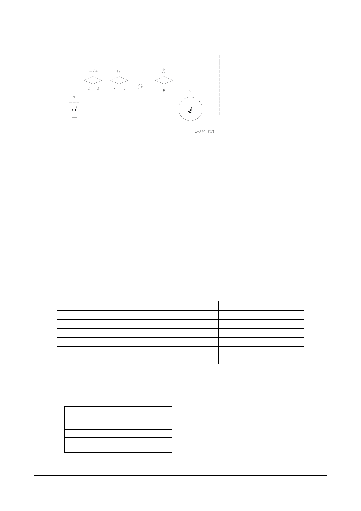
B. CONTROLS
B-1 Control Panel (Monitor Front Panel)
1. Power LED.
2. Adjust decrease.
3. Adjust increase.
4. Function select anti-clockwise.
5. Function select clockwise.
6. Power ON/OFF switch, push to ON and push to OFF. (Toggle switch)
7. Ear-phone jack.
8. Volume Control.
C. Power Management
C-1 Power Management
1. Meets VESA DPMS Proposal
2. Power Consumption
Meets VESA DPMS Proposal
On-mode 54 W
Stand-by 5 W
Suspend 5 W
Off-mode 5 W
DC power off 5 W
Disconnection 5 W
Power saving states are measured with speakers attached but not working.
The recovery time from stand-by/suspend/off-mode to on-mode is 3 seconds maximum.
Green
max
Yellow
max
Yellow
max
Yellow
max
Dark
max
max
Dark (DC power off)
Yellow (DC power on)
C-2 Power Consumption
Meets VESA DPMS Proposal
On-mode 54 W
Stand-by 5 W
Suspend 5 W
Off-mode 5 W
DC power off 5 W
Disconnection 5 W
1. Measured from AC input end of AC power adapter.
2. Power saving states are measured with speakers attached but not worked.
max
max
max
max
max
max
2
Page 6
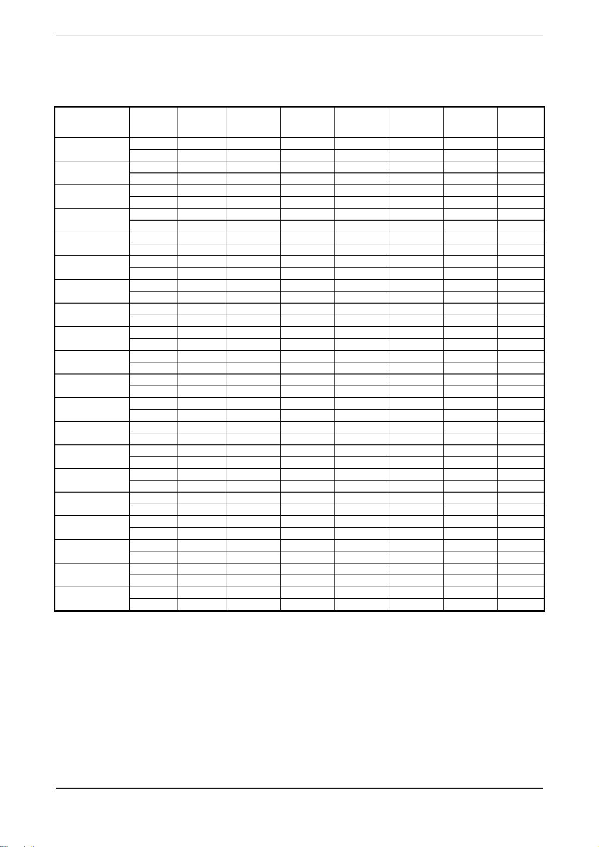
D. Display Modes for Inspections
D-1 Supported Timing
TIMING
640x350 31.469
VGA-350 70.087
640x400 31.469
VGA-GRAPH 70.087
640x400 31.5
NEC PC9821 70.15
640x480 31.469
VGA-480 59.94
640x480 35
APPLE MAC-480 66.67
640x480 37.861
VESA-480-72Hz 72.809
640x480 37.5
VESA-480-75Hz 75
720x400 31.469
VGA-400-TEXT 70.087
832x624 49.725
APPLE MAC-800 74.55
800x600 35.156
SVGA 56.25
800x600 37.879
VESA-600-60Hz 60.317
800x600 48.077
VESA-600-72Hz 72.188
800x600 46.875
VESA-600-75Hz 75
1024x768 48.363
XGA 60.004 - 806 768 6 3 29
1024x768 53.964
COMPAQ-XGA 66.132
1024x768 56.476
VESA-768-70Hz 70.069
1024x768 60.023
VESA-768-75Hz 75.029
1024x768 60.24
APPLE MAC-768 75.02
1280x1024 64
VESA-1024-60Hz 60
1280x1024 80
VESA-1024-75Hz 75
FH (KHZ) SYNC TOTAL ACTIVE SYNC FRONT BACK PIXEL
FV (HZ) POLARITY (DOT/LINE) (DOT/LINE)
+
-
+
-
-
-
-
-
-
-
-
-
-
+
-
+
+
+
+
+
+
+
+
-
+
+
-
+
+
-
+
+
+
+
800 640 96 16 48 25.175
449 350 2 37 60
800 640 96 16 48 25.175
449 400 2 12 35
800 640 64 16 80 25.197
449 400 2 13 34
800 640 96 16 48 25.175
525 480 2 10 33
832 640 40 24 128 31.5
520 480 3 9 28
832 640 40 16 120 31.5
520 480 3 1 20
840 640 64 16 120 31.5
500 480 3 1 16
900 720 108 18 54 28.322
449 400 2 12 35
1152 832 64 32 224 57.2832
667 624 3 1 39
1024 800 72 24 128 36
625 600 2 1 22
1056 800 128 40 88 40
628 600 4 1 23
1040 800 120 56 64 50
666 600 6 37 23
1056 800 80 16 160 49.5
625 600 3 1 21
1344 1024 136 24 160 65
1328 1024 176 16 112 71.664
816 768 4 8 36
1328 1024 136 24 144 75
806 768 6 3 29
1312 1024 96 16 176 78.75
800 768 3 1 28
1328 1024 96 32 176 80
803 768 3 3 29
1688 1280 112 48 248 108
1066 1024 3 1 38
1688 1280 144 16 248 135
1066 1024 3 1 38
WIDTH
(DOT/LINE)
PORCH
(DOT/LINE)
PORCH
(DOT/LINE)
FOREQ.
(MHZ)
If the input timing is not a supported timing listed above but within the supported frequency range
(Horizontal: 80KHz, Vertical: 85Hz), this monitor will select a closest mode instead. However, the
display quality may not be optimised.
3
Page 7
E. Dot Defects & Audio Specification
E-1 Dot Defects on LCD Panel
Visual
Defect
Electrical
Defect
Foreign Material
Bubble
Scratch
Bright Line
Dark Line
Bright Dot None
Double Bright Dot
Three Bright Dots None
Dark Dot
Double Dark Dot
Three Dark Dots
Distance of B/D to B/D
Distance of D/D to D/D
0.1=<D=<1.0
D=<1.0
N=<6
0.01=<W=<0.1
0.3=<L=<7
N=<4
0.05=<W=<0.1
0.3=<L=<7
N=<4
N=<2
N=<10
N=<3
N=<1
S>=10mm
S>=5mm
Note:
W : Width (mm)
L : Length (mm)
D : Diameter (mm)
N : Number (pcs)
B/D: Bright Dot
D/D: Dark Dot
E-2 Audio Specifications
Conditions 1KHz, volume max, Load 8W speakers x2
Audio Input 500mV
Audio Output 2x 0.5W
Frequency Response 50Hz to 20KHz ±3dB
S/N Ratio -70dB max
Cross Talk -40dB max
Distortion 1% max
rms
max
4
Page 8
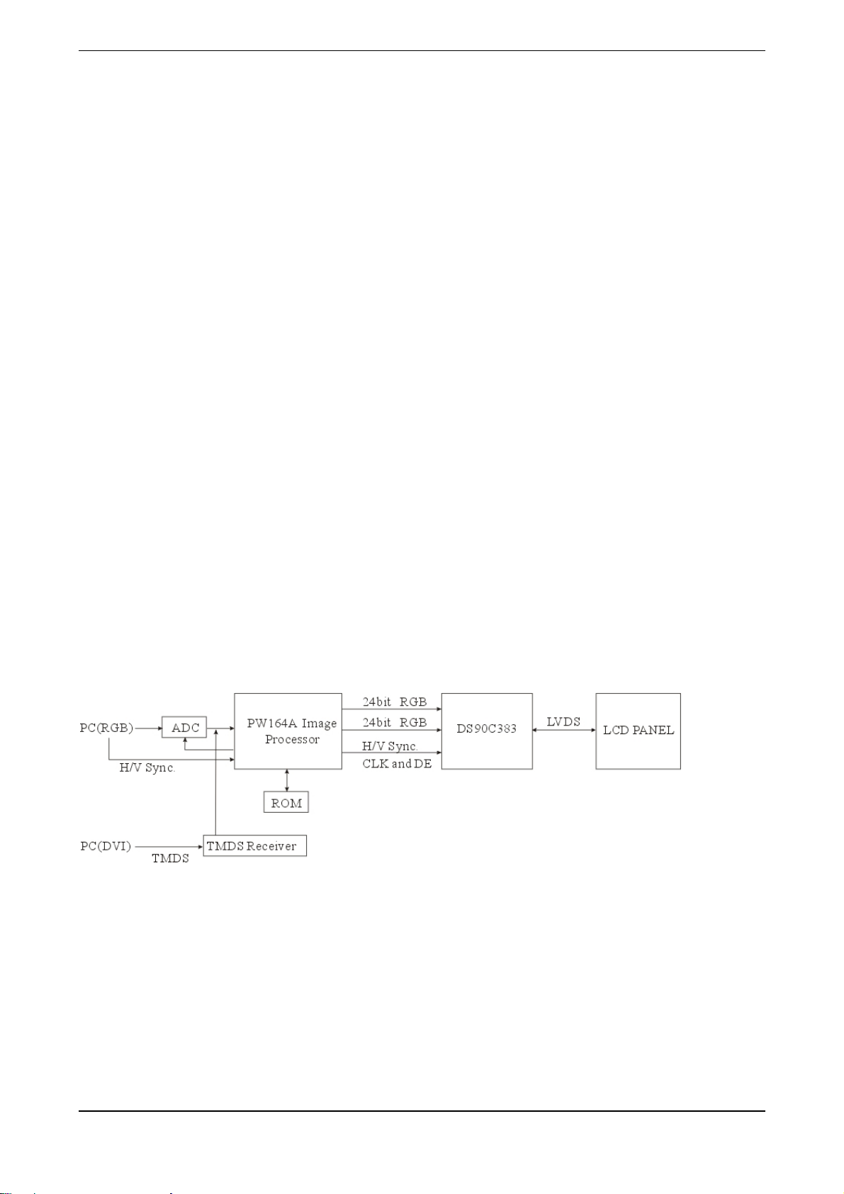
2. MAIN / DISPLAY CONTROL BOARD - VL-706
A. Description
The VL-706 display control board is design to directly convert analog RGB signals from a
standard VGA display card to optimum LCD timing signals so as to construct a high display
quality LCD monitor.
B. Features
•
On-board embedded micro-processor to detect display timings and control user
functions.
• Uses Pixelworks design to generate optimum LCD timings.
• Uses EEPROM to memorise every adjusted parameter.
• Supports up to 22 display modes from VGA to SXGA.
• Offers full screen expansion function on non-SXGA mode (automatic).
• Flexible colour temperature selection function including 9300º, 6500º and user mode.
• Supports OSD functions.
• Supports VESA DPMS function.
• Supports DDC1/2B functions.
• Supports 5 languages for OSD description.
• The longest time for mode change is 3 seconds.
C. Block Diagram
5
Page 9
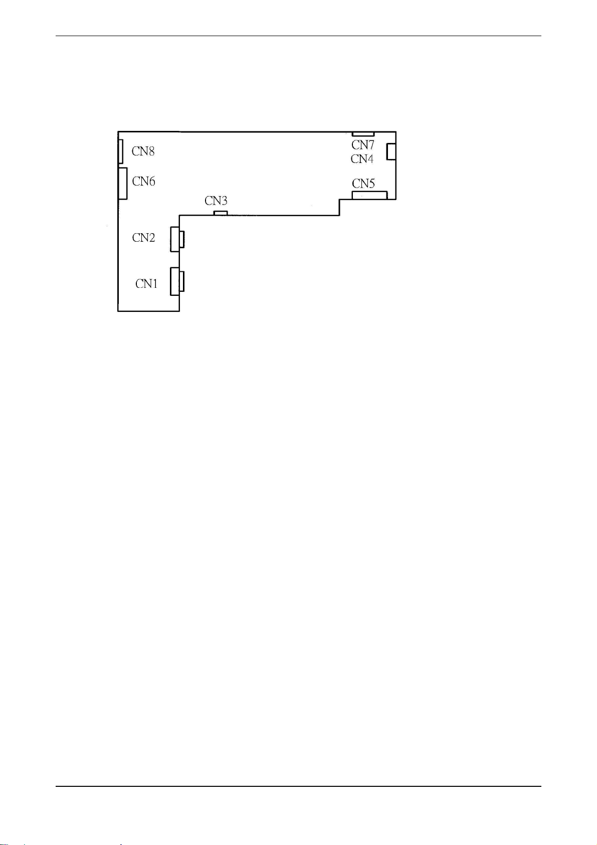
D. Connector Locations
E. Connector Type
Location Type Maker Number of Pins
CN2 1211-15 E&T 15
CN1 74320-1004 FEMALE 30
CN8 96113-1203 E&T 12
CN3 96113-0513 E&T 5
CN7 96113-1003 E&T 10
CN4 96118-0413 E&T 4
CN5 98210-3011 E&T 30
F. Connector Pin Assignment
F-1 CN2
Pin No. Signal Comment
1 R-Video Red Video Input.
2 G-Video Green Video Input.
3 B-Video Blue Video Input.
4 NC
5 PCDETECT PCDETECT Input.
6 Ground Ground.
7 Ground Ground.
8 Ground Ground
9 5VCC DDC Power Input.
10 Ground Ground.
11 NC
12 SDA DDC 1/2B
13 HS Horizontal Sync Input.
14 VS Vertical Sync Input.
15 SCL DDC 2B
6
Page 10
F-2 CN5
Terminal No. Symbol Function
28,29,30 VDD 5V POWER SUPPLY
1 TXE0- LVDS EVEN OUTPUT DATA PAIRS
2 TXE0+ LVDS EVEN OUTPUT DATA PAIRS
3 TXE1- LVDS EVEN OUTPUT DATA PAIRS
4 TXE1+ LVDS EVEN OUTPUT DATA PAIRS
5 TXE2- LVDS EVEN OUTPUT DATA PAIRS
6 TXE2+ LVDS EVEN OUTPUT DATA PAIRS
8 TXECLK- LVDS EVEN OUTPUT DATA PAIRS
9 TXECLK+ LVDS EVEN OUTPUT DATA PAIRS
10 TXE3- LVDS EVEN OUTPUT DATA PAIRS
11 TXE3+ LVDS EVEN OUTPUT DATA PAIRS
12 TXO0- LVDS ODD OUTPUT DATA PAIRS
13 TXO0+ LVDS ODD OUTPUT DATA PAIRS
15 TXO1- LVDS ODD OUTPUT DATA PAIRS
16 TXO1+ LVDS ODD OUTPUT DATA PAIRS
18 TXO2- LVDS ODD OUTPUT DATA PAIRS
19 TXO2+ LVDS ODD OUTPUT DATA PAIRS
20 TXOCLK- LVDS ODD OUTPUT DATA PAIRS
21 TXOCLK+ LVDS ODD OUTPUT DATA PAIRS
22 TXO3- LVDS ODD OUTPUT DATA PAIRS
23 TXO3+ LVDS ODD OUTPUT DATA PAIRS
7,14,17,24 GND Ground
25,26,27 GND Ground
F-3 CN1
Pin Signal Assignment Pin Signal Assignment Pin Signal Assignment
1 TMDS Data2- 9 TMDS Data1- 17 TMDS Data02 TMDS Data2+ 10 TMDS Data1+ 18 TMDS Data0+
3 TMDS Data2/4 Shield 11 TMDS Data1/3 Shield 19 TMDS Data0/5 Shield
4 TMDS Data4- 12 TMDS Data3- 20 TMDS Data55 TMDS Data4+ 13 TMDS Data3+ 21 TMDS Data5+
6 DDC Clock 14 +5V Power 22 TMDS Clock Shield
7 DDC Data 15 PC DETECT 23 TMDS Clock+
8 Not Connect 16 Hot Plug Detect 24 TMDS Clock-
F-4 CN8
Pin No. Signal Comment
1,2,3 12 VCC Inverter Power Output.
4 BLON Bright Light ON/OFF.
5,6,10,11,12 GND GND
7,8 5 VCC Inverter Power Output.
9 BRIGHT Brightness Adjustment.
7
Page 11
F-5 CN4
Pin No. Signal Comment
1 12 VCC 12 VCC Power Input
2 5 VCC 5V Power Input
3 GND GND
4 GND GND
F-6 CN7
Pin No. Signal Comment
1 MUTE Volume ON/OFF control
2 LED-Y Power saving mode
3 LED-G Monitor is ON
4 GND GND
5 KEY-UP Function select anti-clockwise key
6 KEY-DOWN Function select anti-clockwise key
7 KEY-R Adjust up key
8 KEY-L Adjust down key
9 KEY-POWER Power ON/OFF key
10 GND GND
3. CONTROL PANEL AND AUDIO CONTROL (KEY BOARD) VK-517
A. Description
The VK-517 is designed to offer a user interfaced control panel that passes and receives signals
to and from VL-706 display control board. Also there is a stereo audio amplifier to drive a pair
of speakers. When in power saving mode, the audio circuit can be turned off by the control
signal from VL-706 board.
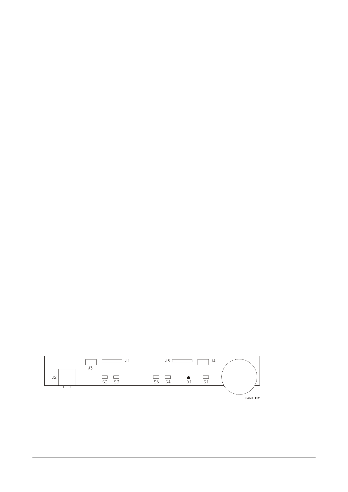
B. Connector and Swi t ch Locati ons
8
Page 12

C. Connector Type
Location Type Maker Number of Pins
J1 96113-1113 E&T 11
J2 SCJ-0348-C SC 9
J3 87502-0200 ACES 2
J4 87502-0200 ACES 2
J5 96113-1013 E&T 10
D. Connector Pin Assignment
D-1 J1
Pin No. Signal Comment
1 VOL Volume ON/OFF control
2 GND GND
3 RIN1 Audio volume adjust line INR
4 LIN1 Audio volume adjust line INL
5 RIN2 Audio volume adjust line OUTR
6 LIN2 Audio volume adjust line OUTL
7 GND GND
8 R-EAR EAR phone out R
9 L-EAR EAR phone out L
10 ROUT Speaker out R
11 LOUT Speaker out L
D-2 J5
Pin No. Signal Comment
1 MUTE Volume ON/OFF control
2 LED-Y Power saving mode.
3 LED-G Monitor on mode.
4,10 GND GND
5 KEY-UP Function select up to VL-706
6 KEY-DOWN Function select down to VL-706
7 KEY-R Function select right to VL-706
8 KEY-L Function select left to VL-706
9 KEY-PWR Power ON/OFF signal to VL-706
9
Page 13

D-3 J3 and J4
Pin No. Signal Comment
1 GND GND
2 OUTL (OUTR) Speaker Out
D-4 J2
Pin No. Signal I/O Comment
1 GND Ground
2 LI 2 Earphone out L
3 RI 2 Earphone out R
4 LI 1 Earphone out L
5 LO Speaker out L
6 NC Not connected
7 RI 1 Earphone out R
8 RO Speaker out R
D-5 Switch Definition
Location Definition
S1 Power ON/OFF
S2 Function select by clockwise direction
S3 Function select by anti-clockwise direction
S4 Adjust up
S5 Adjust down
D-6 LED Definition
Location Definition
D1 Green for ON-mode; Dark for DC power off; Yellow for stand-by; suspend; off-mode.
D-7 Variable Resistor
VR1: Volume control, clockwise for increasing; anti-clockwise for decreasing
10
Page 14

D-8 Electrical Characteristics (T
amb
=25
°°°°
C)
Audio amplifier (Use Panasonic VP-7723A Audio Analyzer).
Item Audio Input Freq. Spec. Comment
Min. Typ. Max.
Input Voltage (V) 11.4 12 12.6
Input Current (mA) 500 800
Audio Voltage Gain 500mV
Frequency Response 100mV
Signal to Noise Ratio 500mV
Crosstalk 100mV
Distortion 500mV
Output Wattage 500mV
Volume Control Analog
1KHz 14dB
rms
50Hz~20KHz -3dB +3dB
rms
1KHz -70dB
rms
1KHz -60dB
rms
1KHz 1%
rms
1KHz 0.5W
rms
4. POWER AND A UDIO BOARD - VM-517
A. Major Specification
Input voltage: 12V ±5% from adapter (LSE 9901B1260)
Volume Max. Load 8Ω
Volume Max. Load 8Ω
Volume Max. Load 8Ω
Volume Max. Load 8Ω
Volume Max. Load 8Ω
Volume Max. Load 8Ω
Input current: 5A max.
Output:
ITEM Output Voltage Max Load. Min Load Tolerance Ripple & Noise (max)
VCC +5.1V 1.9A 0.19A ±5% 150mV
p-p
B. Description
The VM-517 is designed to supply the power to the VL-706 display control board. Under the
control of VL-706, it can run into power saving mode so as to save the power of the whole
monitor.
C. Efficiency
80% minimum at Maximum Load.
D. Connector Locations
11
Page 15

E. Connector Type
Location Type Maker Number of Pins
J801 DC-IN SC 2
J3 SCJ-0345-1-X-S SC 3
J2 96113-1103 E&T 11
J802 B4B-XH-A JST 4
F. Connector Pin Assignment
F-1 J801 DC 12V Input
Pin No. Signal Comment
Pin 1 +12V From adapter output cable
Pin 2 GND From adapter output cable
F-2 J802 FOR I/F Circuit
Pin No. Signal Comment
Pin 1 +12V From adapter +12V Power
Pin 2 +5.1V Supply for I/F Circuit
Pin 3, 4 GND GND
F-3 J3 FOR Audio input
Pin No. Signal Comment
Pin 1 GND GND
Pin 2 Audio IN (1) From Audio output (1)
Pin 3 Audio IN (2) From Audio output (2)
F-4 J2 TO Speaker Circuit
Pin No. Signal Comment
Pin 1 VOL Volume ON/OFF control
Pin 2 GND GND
Pin 3 RIN1 Audio volume adjust line INR
Pin 4 LIN1 Audio volume adjust line INL
Pin 5 RIN2 Audio volume adjust line OUTR
Pin 6 LIN2 Audio volume adjust line OUTL
Pin 7 GND GND
12
Page 16

Pin 8 R-EAR EAR phone out R
Pin 9 L-EAR EAR phone out L
Pin 10 ROUT Speaker out R
Pin 11 LOUT Speaker out L
5. INVERTER BOARD - AMBIT T51I036.00
A. Description
The T51I036.00 Inverter board is designed for lighting up the back-lights of LCD module.
B. Electrical Characteristics
B-1 FOR UNIPAC PANEL (UM170E01)
MIN. TYP. MAX. COMMENT
INPUT VOLTAGE 11.4V 12.0V 12.6V 12V ±5%
INPUT CURRENT -------- 2.1A _ Vin=12V, Vbrite=0V
Normal BACKLIGHT
VOLTAGE
LAMP CURRENT
DRIVING
FREQUENCY
EFFICIENCY -------- 78% --------
PWM dimming
frequency
Vin ON/OFF sequence -------- 0.5S --------
OLP TIME -------- 1S _
BRIGHTNESS RANGE 20% -------- 100%
Brightness control 0V _ 4V 0V, brightness max.
Brightness _ 250 cd/m
Strike voltage at 0°C _ _ 1250 V
Strike voltage at 25°C _ _ 950 V
-------- 710 V
--------. 12mA
45KHz 52KHz 60KHz
120Hz 140Hz 160Hz
--------
rms
--------
rms
2
_
rms
rms
Total two lamps for
Unipac
Vin = 12V, max
brightness
Open lamp protection
time
Operating life time 50,000 hrs _ _ (note)
Note:
Life-time (hr) can be defined as the time in which it continues to operate under the condition:
Ta=25 ±2°C, IL =12 mA
1. When the brightness becomes 50%
2. When the startup voltage (Vs) at 0°C becomes higher than the maximal value of Vs specified above.
until one of the following event occurs:
rms
13
Page 17

B-2 FOR SAMSUNG PANEL (LT170E2-131)
MIN. TYP. MAX. COMMENT
INPUT VOLTAGE 11.4V 12.0V 12.6V 12V ±5%
INPUT CURRENT -------- 2.2A -------- Vin=12V, Vbrite=4V
Normal BACKLIGHT
VOLTAGE
LAMP CURRENT
(every lamp)
DRIVING
FREQUENCY
EFFICIENCY -------- 78% --------
PWM dimming
frequency
-------- 690V
2mA
6.5mA
rms
--------
rms
7mA
rms
Each CCFL
rms
30KHz 50KHz 80KHz
Vin = 12V, max
brightness
120Hz 140Hz 160Hz
Vin ON/OFF sequence -------- 0.5S --------
OLP TIME -------- 1S --------
Open lamp protection
time
BRIGHTNESS RANGE 20% -------- 100%
Brightness control 0V _ 3.75V
Brightness 170 cd/m2 200 cd/m
2
_
Strike voltage at 0°C _ _ 1420V
Strike voltage at 25°C _ _ 1100V
rms
rms
3.75V, brightness
max.
Operating life time 20,000 hrs _ _ (note)
Note:
Life-time (hr) can be defined as the time in which it continues to operate under the condition:
Ta=25±2°C, IL =6.5mA
until one of the following event occurs:
rms
1.When the brightness becomes 50%
2.When the startup voltage (Vs) at 0°C becomes higher than the maximal value of Vs specified above.
14
Page 18

B-3 FOR ACER PANEL (L170E3-1)
MIN. TYP. MAX. COMMENT
INPUT VOLTAGE 11.4V 12.0V 12.6V 12V ±5%
INPUT CURRENT -------- 1.7A _ Vin=12V, Vbrite=3.75V
Normal BACKLIGHT
VOLTAGE
LAMP CURRENT
(every lamp)
DRIVING
FREQUENCY
-------- 720V
6.1mA
3mA
rms
40KHz 50KHz 60KHz
EFFICIENCY -------- 75% -------PWM dimming
frequency
150Hz 170Hz 190Hz
--------
rms
6.6mA
rms
Each CCFL
rms
Vin = 12V, max
brightness
Vin ON/OFF sequence -------- 0.5S --------
OLP TIME -------- 1S -------BRIGHTNESS
RANGE
20% -------- 100%
Open lamp protection
time
Brightness control 0V _ 3.75 V 3.75V, brightness max.
Brightness 200 cd/m2 250 cd/m
Strike voltage at 0°C _ _
Strike voltage at 25°C _ _
2
_
rms
rms
1700V
1200V
Operating life time 50,000 hrs _ _ (note)
Note:
Life-time (hr) can be defined as the time in which it continues to operate under the condition:
Ta=25±2°C, IL =6mA ±0.5mA
until one of the following event occurs:
rms
1.When the brightness becomes 50%
2.When the startup voltage (Vs) at 0°C becomes higher than the maximal value of Vs specified above.
15
Page 19

C. Connector Locations
D. Connector Pin Assignment
D-1 CN1 (ACES, 85205-1200 12P)
Pin No. Signal Comment
1,2,3 BP+ +12V
5,6,10,11,12 GND GND
4 BLT_ON Back-light ON/OFF control, high active (5V)
7 +5VS +5VS
9 BRITE BRITE Brightness (0-5V) control from I/F
0V for maximum brightness
8 NC NC
D-2 CN2 and CN3 (JST SM04(4.0)B-BHS-14P)
Pin No. Signal Comment
1 HV High voltage for lamp
2 HV High voltage for lamp
3 NC NC
4 LV Low voltage (common)
16
Page 20

6. AC ADAPTER (LSL9901B12320)
A-1 Specification Review
• Input voltage
Single phase, 50/60HZ, 100VAC to 240VAC ±10%
• Input current
1.5A (max) at 90VAC input and full load 0.75A (max) at 264 VAC input and full
load.
• Inrush current @ cold start
30A (0-peak) @ 110Vac, 50A (0-peak) @ 220Vac
• Output
Tolerance Output Current
Output Volt - MIN MAX
+12Vdc ±5% 0A 5A 11.4~12.6Vdc
• Total output power: 60Watt max.
• Efficiency: 80% min. @115V/230VAC maximum load.
• Dimensions: 110 (L) x 63 (W) x 31 (H)
7. CIRCUIT DESCRPTION
A. Display Controller
U8 is image processor. The functions of the CHIP support as below:
1. High quality image scalar
2. On-chip 16 bit Microprocessor
3. On-screen display
4. Automatic image optimiser
Volt Tolerance
B. Pl ug and Play Ci rcuit
Plug and play allows the serial communication of host PC and peripherals offering minimal
configurations to end-users. This monitor supports DDC2B communication protocol.
C. System Clock
The U11 (130MHz) & U13 (104 MHz) supports the U8 reference clock.
D. Power Regulator
1. The U15, U18 (APL1085) & U17 (APL5883) are linear regulators that converts input
voltage from 5V to 3.3V.
2. The U16 (APL1117) is linear regulator that converts input voltage from 5V to 2.5V.
17
Page 21

8. INTRODUCTION
A. Front Panel Control and LED
Front Panel Controls
Item Control Function
1 Power Switch Turns the monitor on and off.
2 Power LED 1. Green indicates monitor is on.
2. Dark indicates DC power is off.
3. Yellow indicates stand-by, suspend or off-mode.
3
Function Button Launches OSD function menu
4
5 Plus Button Selects and adjusts the functions
6 Minus Button Selects and adjusts the functions
18
Page 22

B. Rear Panel connector Input Signals
Rear Panel Cable and Connector
Item Cable / Connector Function
1
2
3
Signal Connector Connects the video cable
Power Connector
Audio Connector Connects the audio cable
Connects the adapter cable
19
Page 23

9. TROUBLESHOOTING
A. Main Procedure
20
Page 24

A-1 Power Circuit Troubleshooting
21
Page 25

A-2 Backlight Troubleshooting
22
Page 26

A-3 Performance Troubleshooting
23
Page 27

A-4 Function Troubleshooting
24
Page 28

THE UPDATED PARTS LIST
FOR THIS MODEL IS
AVAILABLE ON ESTA
Page 29

Audio B oard
connect or
J2
4 5
J1
11
10
LOUT
R OU T
9
L _E AR
8
R _EAR
7
L IN_ 2
6
5
4
3
2
1
2
1
1
E
3
L I1 L O
2
L I2
7
R I1
3
R I2
S CJ-0348-C
NC
R O
GND
6
8
1
J3
1
2
ACE S _87502_0200
S T R AIGHT /2.5
J4
1
2
ACE S _87502_0200
S T R AIGHT /2.5
R
M a i n B o a r
c o n n e c t o
E & T _ 9 6 1 1 3 _ 1 1 1
J
M U T
L E D _
L E D _
G N
K E Y _ U
K E Y _ D O W
K E Y _
K E Y _
K E Y _ P W
G N
1
E & T _ 9 6 1 1 3 _ 1 0 1
R I N _
L I N _
R I N _
M U T
1
'
5
d
1
r
2
3
4
5
6
7
8
9
0
S
P T - 0 0 2 - B
S
P T - 0 0 2 - B
E
Y
G
D
P
R
L
D
3
N
R
S
P T - 0 0 2 - B
S
S
P T - 0 0 2 - B
V
321
1
S
P T - 0 0 2 - B
S
3 3 ' 2 ' 2
1
2
2
2
Y G 2 0 9 3 Y E L / G R
1
3
2
6
2
4
2
5
2
7
2
N
P T - 0 0 2 - B
P T - 0 0 2 - B
No. 0418
VK 517 Key Board
HITACHI
Page 30

No. 0418
VL-706 VGA Input
HITACHI
Page 31

No. 0418
VL-706 ADC
HITACHI
Page 32

No. 0418
VL-706 TMDS
HITACHI
Page 33

No. 0418
VL-706 Scaler and MCU
HITACHI
Page 34

No. 0418
VL-706 Flash ROM
HITACHI
Page 35

No. 0418
VL-706 MSIC
HITACHI
Page 36

No. 0418
VL-706 Power
HITACHI
Page 37

No. 0418
VL-706 LVDS
HITACHI
Page 38

No. 0418
VL-706 Keyboard
HITACHI
Page 39

No. 0418
VM-517 DC-DC
HITACHI
Page 40

No. 0418
VM-517 Audio Amp
HITACHI
Page 41

Hitachi, Ltd. Tokyo, Japan
International Sales Division
THE HITACHI ATAGO BUILDING,
No. 15 –12 Nishi Shinbashi, 2 – Chome,
Minato – Ku, Tokyo 105-8430, Japan.
Tel: 03 35022111
HITACHI EUROPE LTD,
Whitebrook Park
Lower Cookham Road
Maidenhead
Berkshire
SL6 8YA
UNITED KINGDOM
Tel: 01628 643000
Fax: 01628 643400
Email: consumer-service@hitachi-eu.com
HITACHI EUROPE GmbH
Munich Office
Dornacher Strasse 3
D-85622 Feldkirchen bei München
GERMANY
Tel: +49-89-991 80-0
Fax: +49-89-991 80-224
Hotline: +49-180-551 25 51 (12ct/min)
Email: HSE-DUS.service@hitachi-eu.com
HITACHI EUROPE srl
Via Tommaso Gulli N.39, 20147
Milano, Italia
ITALY
Tel: +39 02 487861
Tel: +39 02 38073415 Servizio Clienti
Fax: +39 02 48786381/2
Email: customerservice.italy@hitachi-eu.com
HITACHI EUROPE S.A.S
Lyon Office
B.P. 45, 69671 BRON CEDEX
FRANCE
Tel: +33 04 72 14 29 70
Fax: +33 04 72 14 29 99
Email: france.consommateur@hitachi-eu.com
HITACH EUROPE AB
Egebækgård
Egebækvej 98
DK-2850 Nærum
DENMARK
Tel: +45 43 43 6050
Fax: +45 43 60 51
Email: csgnor@hitachi-eu.com
Hitachi Europe Ltd
Bergensesteenweg 421
1600 Sint- Pieters-Leeuw
BELGIUM
Tel: +32 2 363 99 01
Fax: +32 2 363 99 00
Email: sofie.van.bom@hitachi-eu.com
www.hitachidigitalmedia.com
HITACHI EUROPE S.A.
364 Kifissias Ave. & 1, Delfon Str.
152 33 Chalandri
Athens
GREECE
Tel: 1-6837200
Fax: 1-6835964
Email: service.hellas@hitachi-eu.com
HITACHI EUROPE S.A.
Gran Via Carlos III, 86, planta 5
Edificios Trade - Torre Este
08028 Barcelona
SPAIN
Tel: +34 93 409 2550
Fax: +34 93 491 3513
Email: atencion.cliente@hitachi-eu.com
HITACHI Europe AB
Box 77 S-164 94 Kista
SWEDEN
Tel: +46 (0) 8 562 711 00
Fax: +46 (0) 8 562 711 13
Email: csgswe@hitachi-eu.com
HITACHI EUROPE LTD (Norway) AB
STRANDVEIEN 18
1366 Lysaker
NORWAY
Tel: 67 5190 30
Fax: 67 5190 32
Email: csgnor@hitachi-eu.com
HITACHI EUROPE AB
Neopoli / Niemenkatu 73
FIN-15140 Lahti
FINLAND
Tel : +358 3 8858 271
Fax: +358 3 8858 272
Email: csgnor@hitachi-eu.com
HITACHI EUROPE LTD
Na Sychrove 975/8
101 27 Praha 10 – Bohdalec
CZECH REPUBLIC
Tel: +420 267 212 383
Fax: +420 267 212 385
Email: csgnor@hitachi-eu.com
 Loading...