

Page 1
No. 0504
SERVICE MANUAL
WARTUNGSHANDBUCH
CAUTION:
hnician read
Avant d’effectuer l’entretien du châassis, le technicien doit lire les
s
VORSICHT:
Vor
“
Data contained within this Service
eration for
Les données fournies dans le
présent manuel d’entretien
peuvent faire l’objet de
modifications en vue de
tungshandbuch
enthaltenen Spezifikationen
nnen sich zwecks
Verbesserungen
ä
ndern.
CML170SXW
Before servicing this chassis, it is important that the service tec
the “Safety Precautions” and “Product Safety Notices” in this service manual.
ATTENTION:
«Précautions de sécurité» et les «Notices de sécurité du produit» présenté
dans le présent manuel.
Öffnen des Gehäuses hat der Service-Ingenieur die „Sicherheitshinweise
und „Hinweise zur Produktsicherheit“ in diesem Wartungshandbuch zu lesen.
MANUEL D’ENTRETIEN
manual is subject to alt
improvement.
perfectionner le produit.
Die in diesem War
kö
October 2000
Page 2

ENGLISH
SAFETY PRECAUTIONS
WARNING: The following precautions must be observed.
ALL PRODUCTS
Before any service is performed on the chassis an
isolation transformer should be inserted between the
power line and the product.
1. When replacing the chassis in the cabinet, ensure
all the protective devices are put back in place.
2. When service is required, observe the original
lead dressing. Extra precaution should be taken to
ensure correct lead dressing in any high voltage
circuitry area.
3. Many electrical and mechanical parts in
HITACHI products have special safety related
characteristics. These characteristics are often not
evident from visual inspection, nor can the
protection afforded by them necessarily be
obtained by using replacement components rated
for higher voltage, wattage, etc. Replacement
parts which have these special safety
characteristics are identified by marking with a
! on the schematics and the replacement parts
list.
The use of a substitute replacement component
that does not have the same safety characteristics
as the HITACHI recommended replacement one,
shown in the parts list, may create electrical
shock, fire, X-radiation, or other hazards.
4. Always replace original spacers and maintain lead
lengths. Furthermore, where a short circuit has
occurred, replace those components that indicate
evidence of overheating.
5. Insulation resistance should not be less than 2M
ohms at 500V DC between the main poles and
any accessible metal parts.
6. No flashover or breakdown should occur during
the dielectric strength test, applying 3kV AC or
4.25kV DC for two seconds between the main
poles and accessible metal parts.
7. Before returning a serviced product to the
customer, the service technician must thoroughly
test the unit to be certain that it is completely safe
to operate without danger of electrical shock. The
service technician must make sure that no
protective device built into the instrument by the
manufacturer has become defective, or
inadvertently damaged during servicing.
CE MARK
1. HITACHI products may contain the CE mark on
the rating plate indicating that the product
contains parts that have been specifically
approved to provide electromagnetic
compatibility to designated levels.
2. When replacing any part in this product, please
use only the correct part itemised in the parts list
to ensure this standard is maintained, and take
care to replace lead dressing to its original state,
as this can have a bearing on the electromagnetic
radiation/immunity.
PICTURE TUBE
1. The line output stage can develop voltages in
excess of 25kV; if the E.H.T. cap is required to be
removed, discharge the anode to chassis via a
high value resistor, prior to its removal from the
picture tube.
2. High voltage should always be kept at the rated
value of the chassis and no higher. Operating at
higher voltages may cause a failure of the picture
tube or high voltage supply, and also, under
certain circumstances could produce X-radiation
levels moderately in excess of design levels. The
high voltage must not, under any circumstances,
exceed 29kV on the chassis (except for projection
Televisions).
3. The primary source of X-radiation in the product
is the picture tube. The picture tube utilised for
the above mentioned function in this chassis is
specially constructed to limit X-radiation. For
continued X-radiation protection, replace tube
with the same type as the original HITACHI
approved type
4. Keep the picture tube away from the body while
handling. Do not install, remove, or handle the
picture tube in any manner unless shatterproof
goggles are worn. People not so equipped should
be kept away while picture tubes are handled
LASERS
If the product contains a laser avoid direct exposure to
the beam when the cover is open or when interlocks are
defeated or have failed.
i
Page 3

FRANÇAIS
CONSIGNES DE SECURITE
AVERTISSEMENT: vous devez respecter les précautions suivantes
POUR TOUS LES PRODUITS
Avant d’effectuer une intervention d’entretien sur le
châssis, vous devez insérer un transformateur d’isolement
entre la ligne d’alimentation électrique et le produit.
1. Lors de la remontage du châssis dans le coffret,
vérifiez que tous les dispositifs de protection sont
remis en place.
2. Lorsqu’une intervention d’entretien s’avère
nécessaire, respectez l’agencement d’origine des
conducteurs. Vous devez prendre des précautions
supplémentaires pour garantir un agencement correct
des conducteurs dans toutes les zones où des circuits
haute tension sont présents.
3. De nombreux composants électriques et mécaniques
des appareils HITACHI ont des caractéristiques
spéciales de sécurité. Bien souvent, ces
caractéristiques ne sont pas évidentes lors d’un
examen visuel et la protection qu’ils offrent n’est pas
forcément garantie si vous utilisez des composants de
rechange conçus, par exemple, pour une tension plus
élevée, une puissance plus forte. Les pièces de
rechange qui offrent des caractéristiques spéciales de
sécurité sont identifiées par un repérage comportant
le symbole ! sur les schémas et sur la
nomenclature des pièces de rechange.
L’emploi d’un composant de rechange qui ne
respecte pas les mêmes caractéristiques de sécurité
que la pièce de rechange que recommande HITACHI
et qui figure dans la nomenclature risque de
provoquer un choc électrique, un incendie, des rayons
X ou d’autres dangers.
4. Remettez toujours en place les entretoises d’origine
et respectez la longueur des conduites. En outre, à la
suite d’un court-circuit, remplacez les composants
présentant des signes de surchauffe.
5. La résistance d’isolement doit être supérieure ou
égale à 2 méga ohms à 500 V c.c. entre les pôles
principaux et des composants métalliques
accessibles, quels qu’ils soient.
6. Aucun claquage et aucune rupture ne doit se produire
pendant l’essai de résistance diélectrique à la suite de
l’application d’une tension de 3 kV c.a. ou de 4,35
kV c.c. pendant deux secondes entre les pôles
principaux et des composants métalliques
accessibles.
7. Avant de remettre au client un produit qui a fait
l’objet d’un entretien, le technicien qui s’est chargé
de cette intervention doit tester à fond cet ensemble
pour s’assurer qu’il ne présente aucun danger
opérationnel et aucun risque de choc électrique. Ce
technicien doit s’assurer qu’aucun des dispositifs de
protection intégrés à cet instrument par le fabricant
n’est défectueux ou n’a été endommagé de façon
accidentelle lors de l’entretien.
ii
LABEL CE
1. Les produits HITACHI peuvent avoir reçu le label
CE qui figure sur la plaque signalétique pour indiquer
que cet ensemble contient des composants qui ont fait
l’objet d’une homologation spécifique de respect des
normes de compatibilité électromagnétique en
fonction de niveaux bien spécifiés.
2. Lors du remplacement d’un des composants de ce
produit, utilisez uniquement le composant correct
identifié dans la nomenclature afin de maintenir le
respect de cette norme ; en outre, vous devez
également ramener l’agencement des conducteurs à
son état d’origine car cela peut avoir une influence au
niveau des rayonnements électromagnétiques et sur la
protection contre ces rayons.
PICTURE TUBE
1. L’étage de sortie des lignes peut développer des
tensions de plus de 25 kV ; s’il faut retirer le chapeau
de protection contre les tensions extrêmement
élevées, il convient de décharger l’anode contre le
châssis par le biais d’une résistance de forte valeur
avant de déposer ce chapeau du tube image.
2. La haute tension doit toujours se maintenir à la valeur
nominale du châssis et ne pas dépasser cette dernière.
Un fonctionnement à des températures élevées peut
provoquer une défaillance du tube image ou l’entrée
d’une tension élevée. Dans certains cas, cela peut
même provoquer des rayons X d’un niveau
légèrement supérieur aux valeurs de calcul. Cette
haute tension ne doit en aucun cas dépasser 29 kV sur
le châssis (à l’exception des téléviseurs de
projection).
3. La principale source de rayons X de cet appareil est
le tube image. Le tube image employé pour assurer la
fonction susmentionnée dans ce châssis est
spécialement construit pour limiter des rayons X.
Pour maintenir cette protection contre les rayons X, il
faut remplacer le tube d’origine d’un type agréé par
HITACHI par un autre tube de même type.
4. Lors des manipulations, ne tenez jamais le tube
image contre le corps. Pendant toutes les opérations
d’installation, de dépose et de manipulation de ce
tube image, quelle que soit la méthode employée,
vous devez toujours porter des lunettes de sécurité
anti-éclatements. Les personnes qui ne portent pas ce
type de lunettes doivent se tenir à l’écart du tube
image lors de la manipulation de ce dernier.
RAYONS LASER
Si ce produit contient un rayon laser, évitez toute
exposition directe à ce faisceau lors de l’ouverture du
couvercle ou lors de l’élimination des verrouillages de
sécurité ou après défaillance de ces verrouillages.
Page 4

DEUTSCH
SICHERHEITSVORKEHRUNGEN
WARNUNG: Die folgenden Vorkehrungen müssen eingehalten werden.
ALLE PRODUKTE
Bevor die Grundplatte gewartet wird, sollte ein Trenntrafo
zwischen die Netzleitung und das Produkt eingebracht
werden.
1. Wenn die Grundplatte in das Gehäuse zurückgestellt
wird, stellen Sie sicher, dass alle
Schutzvorrichtungen wieder an ihrem Ort sind.
2. Wenn Wartung erforderlich ist, halten Sie die
originale Verdrahtungsart ein. Besondere Vorsicht ist
nötig, um die korrekte Verdrahtungsart in jedem
Hochspannungsstromkreis zu gewährleisten.
3. Viele elektrische und mechanische Teile von
HITACHI Produkten haben besondere
sicherheitsbezogene Eigenschaften. Diese
Eigenschaften fallen oft nicht ins Auge, aber der
durch sie gewährte Schutz kann nicht unbedingt
erreicht werden, wenn man Ersatzteile benutzt, die
für höhere Spannung, Leistung usw. ausgelegt sind.
Ersatzteile, die diese besonderen
Sicherheitsmerkmale haben, sind in den
Prinzipskizzen und Ersatzteillisten an einem ! zu
erkennen.
Der Gebrauch von Ersatzteilen, die nicht dieselben
Sicherheitsmerkmale haben wie die empfohlenen
HITACHI Ersatzteile, wie sie in der Ersatzteilliste
aufgeführt sind, kann zu elektrischem Schlag, Feuer,
Röntgenstrahlung und anderen Gefahren führen.
4. Immer die originalen Abstandsstücke ersetzen und
die Leitungslängen beibehalten. Wo ein Kurzschluss
passiert ist, die Teile ersetzen, bei denen Überhitzung
nachzuweisen ist.
5. Der Isolierwert sollte bei 500 V Gleichstrom
zwischen den Hauptpolen und allen zugänglichen
Metallteilen nicht unter 2M Ohm liegen.
6. Bei der Prüfung auf Durchschlagsfestigkeit sollte
kein Überschlag oder Durchschlag vorkommen,
wenn zwei Sekunden lang 3 kV Wechselstrom oder
4,25 kV Gleichstrom zwischen den Hauptpolen und
allen zugänglichen Metallteilen angelegt wird.
7. Bevor das gewartete Produkt dem Kunden
zurückgegeben wird, muss der Wartungstechniker
das Gerät gründlich prüfen, um sicherzustellen, dass
es betriebssicher ist ohne das Risiko eines
elektrischen Schlages. Der Wartungstechniker muss
sicherstellen, dass keine vom Hersteller im Gerät
eingebaute Schutzvorkehrung schadhaft geworden ist
oder bei der Wartung unabsichtlich beschädigt
wurde.
CE KENNZEICHEN
1. HITACHI Produkte enthalten eventuell das CE
Kennzeichen auf dem Leistungsschild, welches
angibt, dass das Produkt Teile enthält, die eigens
zugelassen sind, um bis zu einem spezifizierten
Niveau elektromagnetische Störfreiheit zu bewirken.
2. Wenn Sie irgendein Teil in diesem Produkt ersetzen,
benutzen Sie bitte nur das korrekte Teil, das in der
Ersatzteilliste aufgeführt ist, um sicherzustellen, dass
dieser Standard eingehalten wird, und geben Sie acht,
die Verdrahtungsart in ihren ursprünglichen Zustand
zurück zu versetzen, weil das einen Einfluss auf die
elektromagnetische Abstrahlung/Störsicherheit haben
kann.
BILDRÖHRE
1. Die Leitungsausgangsstufe kann Spannungen von
mehr als 25 kV entwickeln; wenn die
Höchstspannungskappe entfernt werden muss,
entladen Sie die Anode zum Gehäuse über einen
hochohmigen Widerstand, bevor Sie sie aus der
Bildröhre entfernen.
2. Hochspannung sollte immer auf den festgelegten
Wert des Gehäuses beschränkt bleiben und nicht
mehr. Betrieb bei höherer Spannung kann zum
Versagen der Bildröhre oder zu hoher
Spannungszufuhr führen und kann unter Umständen
auch Röntgenstrahlung hervorbringen, die leicht über
dem Konstruktionsniveau liegt. Die Hochspannung
darf auf keinen Fall 29 kV am Gehäuse überschreiten
(außer bei Projektionsfernsehern).
3. Die Hauptquelle der Röntgenstrahlung im Produkt ist
die Bildröhre. Die Bildröhre, die für die oben
erwähnte Funktion in diesem Gehäuse benutzt wird,
ist eine Spezialkonstruktion zur Begrenzung der
Röntgenstrahlung. Um den Schutz vor der
Röntgenstrahlung zu behalten, ersetzen Sie bitte die
Röhre durch denselben Typ wie den ursprünglichen
von HITACHI zugelassenen.
8. Halten Sie die Bildröhre bei der Handhabung vom
Körper weg. Sie dürfen die Bildröhre nur dann
installieren, entfernen oder handhaben, wenn Sie eine
nicht splitternde Schutzbrille tragen. Personen ohne
derartigen Schutz sollten ferngehalten werden,
solange Bildröhren gehandhabt werden.
LASER
Wenn das Produkt einen Laser enthält, setzen Sie sich
keinesfalls direkt dem Strahl aus, wenn die Abdeckung
geöffnet ist oder wenn die Verriegelung versagt.
iii
Page 5

1. ELECTRICAL REQUIREMENTS ...................................................1
A. LCD Panel Specification ..................................................................................1
B. Controls............................................................................................................2
C. Power Management.........................................................................................2
D. Display Modes for Inspections ......................................................................... 3
2. VL-701 DISPLAY CONTROL BOARD ........................................ 4
A. Description ....................................................................................................... 4
B. Features ........................................................................................................... 4
C. Block Diagram (Control CKT) .......................................................................... 4
D. Connector Locations ........................................................................................ 5
E. Connector Type................................................................................................ 5
F. Connector Pin Assignment...............................................................................5
3. VK-515 CONTROL PANEL .........................................................7
A. Description ....................................................................................................... 7
B. Connector and Switch Locations...................................................................... 7
C. Connector Type ...............................................................................................7
D. Connector Pin Assignment ..............................................................................8
4. VM-515 POWER and AUDIO BOARD ........................................ 10
A. Major Specification...........................................................................................10
B. Description ....................................................................................................... 10
C. Electrical Characteristics.................................................................................. 10
D. Connector Location..........................................................................................10
E. Connector Type................................................................................................ 11
F. Connector Pin Assignment...............................................................................11
5. PK07006700/ AMBIT T51I036.00 INVERTER BOARD ..............12
A. Description ....................................................................................................... 12
B. Electrical Characteristics..................................................................................12
C. Connector Locations ........................................................................................ 13
D. Connector Pin Assignment ..............................................................................13
6. AC Adapter (LSE9901B1260)..................................................... 14
A. Quick specification review................................................................................14
iv
Page 6

7. CIRCUIT DESCRIPTION ............................................................. 14
A. Display- Controller............................................................................................ 14
B. Circuit of Plug and Play....................................................................................14
C. System Clock ................................................................................................... 14
D. Power Regularator ........................................................................................... 14
8. INTRODUCTION.......................................................................... 15
A. Front Panel Controls and Led .......................................................................... 15
B. Rear Panel Connectors....................................................................................16
9. TROUBLESHOOTING................................................................. 17
A. Main Procedure................................................................................................17
SCHEMATIC CIRCUITS .................................................................22
v
Page 7
17 inch (17” viewable image size): active matrix: thin film transistor
(TFT): liquid crystal display (LCD): 0.264 mm dot pitch: R.G.B.
rast
Active Display
1. ELECTRICAL REQUIREMENTS
A. LCD Panel Specification
Display:
Vertical stripe 200 cd//m2 white luminance, typical: 200:1 cont
ratio, Min.
Compatibility:
Synchronization
Frequencies:
Resolution:
Area:
Viewing Angles:
640 x 350: VGA-350
720 x 400: VGA text
640 x 400: VGA-GRAPH
640 x 480: VGA, 60Hz to 75 Hz vertical refresh rate
800 x 600: 56Hz to 75 Hz vertical refresh rate
1024 x 768 non-interlaced: 60Hz to 75 Hz vertical refresh rate
1280 x 1024 non-interlaced: 60Hz to 75 Hz vertical refresh rate
Horizontal: 24 kHz to 80 kHz
Vertical: 56 Hz to 75 Hz
Pixel Frequency: 21 Mhz 135 Mhz
Horizontal: 1280 dots
Vertical: 1024 lines
Horizontal: 337.92 mm
Vertical: 270.34 mm
Up 40deg down 80deg (TYP)
Display Colors:
Power Supply:
Power
Consumption:
Environmental:
Left 60deg, Right 80deg (TYP)
CR ≥ 10
16,777,216 (with FRC)
AC 100 to 240V worldwide input, 50 / 60Hz
Typical: 25W on mode +10 / -25%
Operating temperature: 0ºC to 50ºC
Storage temperature: -20ºC to 65ºC
Relative Humidity: 20%~80%
1
Page 8
B. CONTROLS
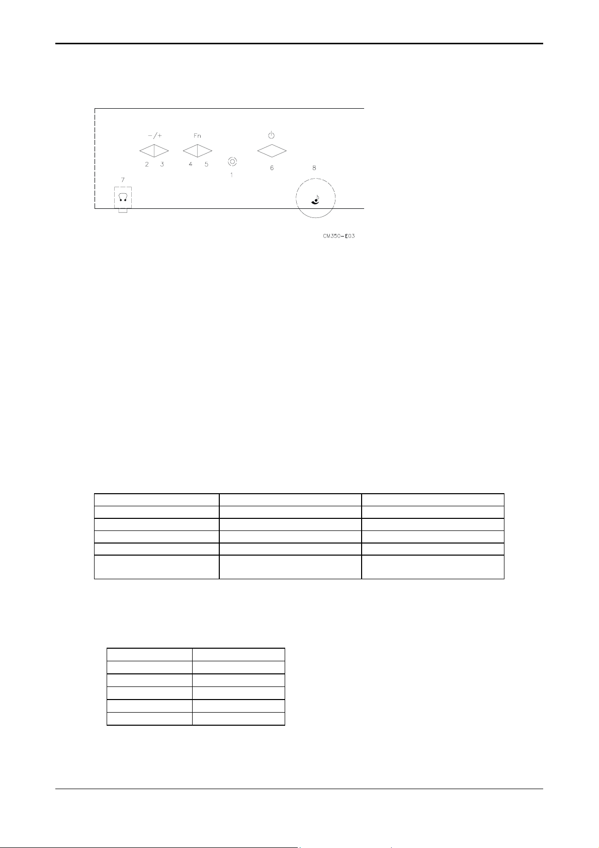
B-1 Control panel (monitor front panel)
1. Power LED
2. Adjust decrease.
3. Adjust increase.
4. Function select counter-clockwise.
5. Function select clockwise.
6. Power ON/OFF switch, push to ON and push to OFF. (toggle switch)
7. Ear phone jack.
8. Volume Control.
C. Power Management
C-1 Power Management
1. Meet VESA DPMS proposal
2. Power Consumption
Meet VESA DPMS Proposal
On mode 54 Wmax Green
Stand-by 5 Wmax Yellow
Suspend 5 Wmax Yellow
Off mode 5 Wmax Yellow
DC power off 5 Wmax Dark
disconnection 5 Wmax
Power saving states are measured with speakers attached but not worked.
The recovery time from stand by /suspend/off mode to on mode is 3 seconds maximun.
C-2 Power Consumption
Meet VESA DPMS Proposal
On mode 54 Wmax
Stand-by 5 Wmax
Suspend 5 Wmax
Off mode 5 Wmax
DC power off 5 Wmax
disconnection 5 Wmax
1. Measured from AC input end of AC power adapter.
2. Power saving states are measured with speakers attached but not worked.
Dark (DC power off)
Yellow (DC power on)
2
Page 9
D. Display Modes for Inspections
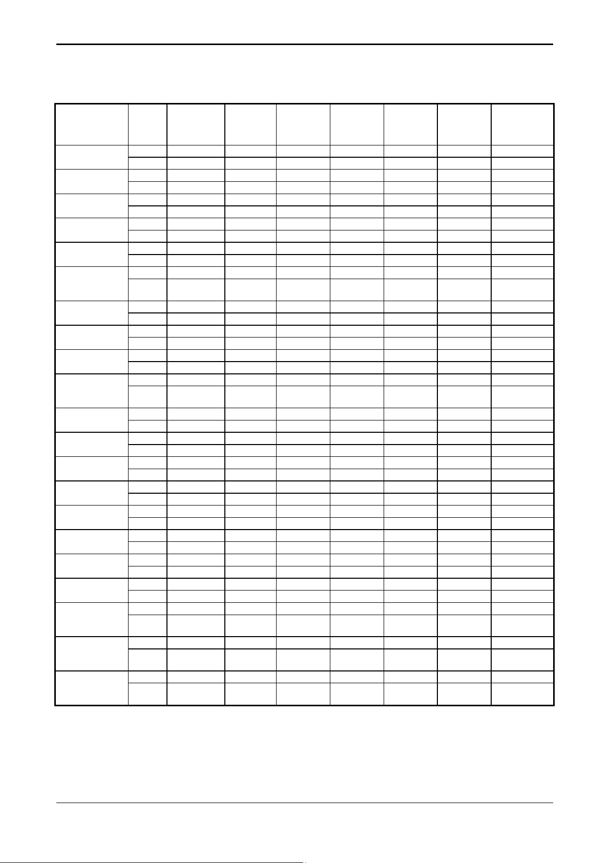
D-1 Supported Timing
TIMING
FV(HZ) POLARITY (DOT/LINE) (DOT/LINE) WIDTH PORCH PORCH FOREQ.(MHZ)
640x350 31.469
VGA-350 70.087
640x400 24.83
NEC PC9801 56.42
640x400 31.469
VGA-GRAPH 70.087
640x400 31.5
NEC PC9821 70.15
640x480 31.469
VGA-480 59.94
640x480 35
APPLE MAC-
480
640x480 37.861
VESA-480-72Hz 72.809
640x480 37.5
VESA-480-75Hz 75
720x400 31.469
VGA-400-TEXT 70.087
832x624 49.725
APPLE MAC800
800x600 35.156
SVGA 56.25
800x600 37.879
VESA-600-60Hz 60.317
800x600 48.077
VESA-600-72Hz 72.188
800x600 46.875
VESA-600-75Hz 75
1024x768 48.363
XGA 60.004
1024x768 53.964
COMPAQ-XGA 66.132
1024x768 56.476
VESA-768-70Hz 70.069
1024x768 60.023
VESA-768-75Hz 75.029
1024x768 60.24
APPLE MAC768
1280x1024 64
VESA-102460Hz
1280x1024 80
VESA-102475Hz
If the input timing is not a supported timing listed above but within the supported frequency range
(Horizontal:80KHz,Vertical:85Hz),this monitor will select a closest mode instead,But the display
quality may not be optimized.
FH(KH
66.67
74.55
75.02
60
75
SYNC TOTAL ACTIVE SYNC FRONT BACK PIXEL
Z)
+
-
-
-
-
+
-
-
-
-
-
-
-
-
-
-
-
+
-
-
+
+
+
+
+
+
+
+
-
-
+
+
-
-
+
+
-
-
+
+
+
+
800 640 96 16 48 25.175
449 350 2 37 60
848 640 64 64 80 21.05
440 400 8 7 25
800 640 96 16 48 25.175
449 400 2 12 35
800 640 64 16 80 25.197
449 400 2 13 34
800 640 96 16 48 25.175
525 480 2 10 33
832 640 40 24 128 31.5
520 480 3 9 28
832 640 40 16 120 31.5
520 480 3 1 20
840 640 64 16 120 31.5
500 480 3 1 16
900 720 108 18 54 28.322
449 400 2 12 35
1152 832 64 32 224 57.2832
667 624 3 1 39
1024 800 72 24 128 36
625 600 2 1 22
1056 800 128 40 88 40
628 600 4 1 23
1040 800 120 56 64 50
666 600 6 37 23
1056 800 80 16 160 49.5
625 600 3 1 21
1344 1024 136 24 160 65
806 768 6 3 29
1328 1024 176 16 112 71.664
816 768 4 8 36
1328 1024 136 24 144 75
806 768 6 3 29
1312 1024 96 16 176 78.75
800 768 3 1 28
1328 1024 96 32 176 80
803 768 3 3 29
1688 1280 112 48 248 108
1066 1024 3 1 38
1688 1280 144 16 248 135
1066 1024 3 1 38
(DOT/LINE) (DOT/LINE) (DOT/LINE)
3
Page 10
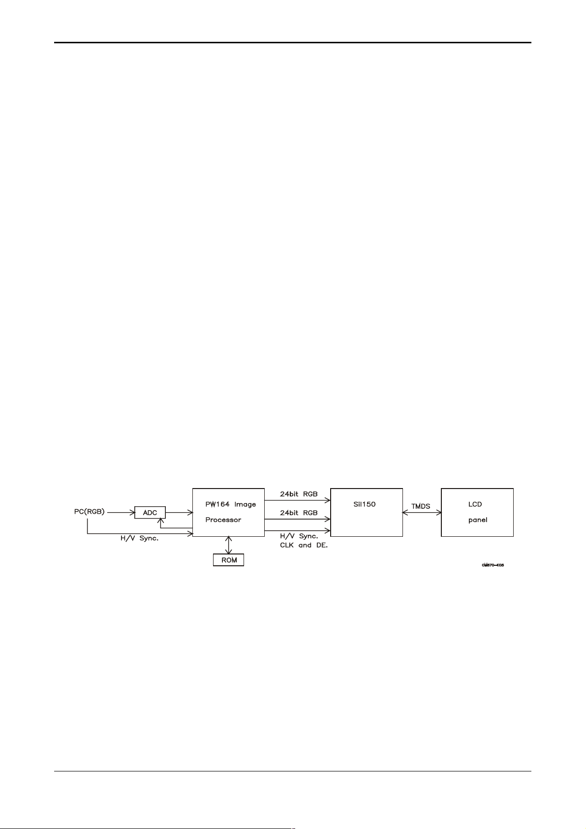
2. VL-701 DISPLAY CONTROL BOARD
A. Description
The VL-701 display control board is design to directly convert the analog RGB signals from
standard VGA display card to optimum LCD timing signals so as to construct a high display
quality LCD monitor.
B. Features
•
On board embedded micro-processor to detect display timings and control user
functions.
• Using Pixelworks design to generate optimum LCD timings.
• Using E
2
PROM to memorize every adjusted parameter.
• support up to 22 display modes from VGA to SXGA.
• Offer full screen expansion function on non-SXGA mode (automatic).
• flexible color temperature selection function including 9300,6500 and user mode.
• Support OSD functions.
• Support VESA DPMS function.
• Support DDC1/2B functions.
• Support 5 languages for OSD description.
• The longest time for mode change is 3 seconds.
C. BLOCK DIAGRAM
4
Page 11
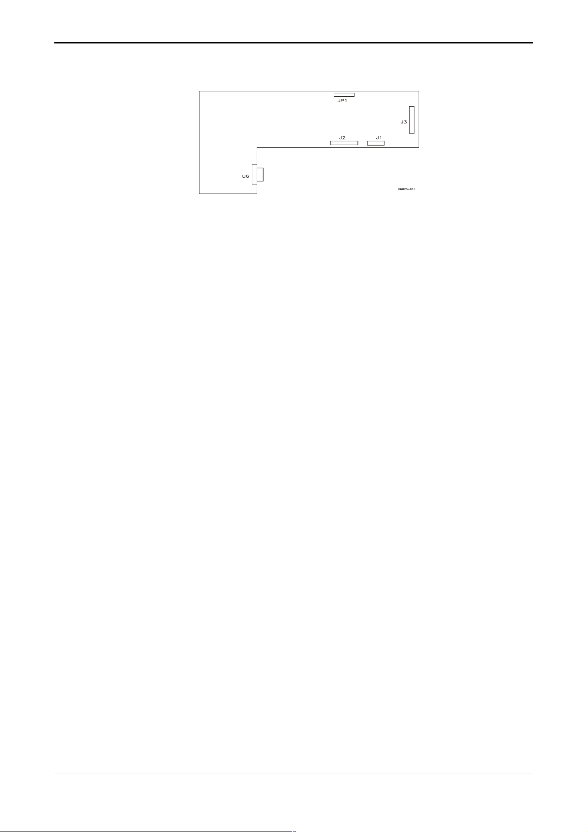
D. Connector Locations
E. Connector Type
Location Type Maker Number of pins
U6 DZ11A91-L8 P1.524 FEMALE 15
JP1 85205-1200 ACES 12
J1 85205-1400 ACES 4
J2 85205-1000 ACES 10
J3 DF14A-25P P1.25 HRS 25
F. Connector pin assignment
F-1 U6
Pin NO. Signal Comment
1 R-Video Red Video Input.
2 G-Video Green Video Input.
3 B-Video Blue Video Input.
4 N. C.
5 PCDETECT PCDETECT Input.
6 Ground Ground.
7 Ground Ground.
8 Ground Ground
9 5VCC DDC Power Input.
10 Ground Ground.
11 NC
12 SDA DDC 1/2B
13 HS Horizontal Sync Input.
14 VS Vertical Sync Input.
15 SCL DDC 2B
5
Page 12
F-2 J3
Terminal No. Symbol Function
1 VDD 5V POWER SUPPLY
2 VDD 5V POWER SUPPLY
3 VDD 5V POWER SUPPLY
4 VDD 5V POWER SUPPLY
5 VDD 5V POWER SUPPLY
6 VDD 5V POWER SUPPLY
7 NC NC
8 GND Ground
9 GND Ground
10 TXC- TMDS output data pairs
11 TXC+ TMDS output data pairs
12 GND Ground
13 GND Ground
14 TX0- TMDS output data pairs
15 TX0+ TMDS output data pairs
16 GND Ground
17 GND Ground
18 TX1- TMDS output data pairs
19 TX1+ TMDS output data pairs
20 GND Ground
21 GND Ground
22 TX2- TMDS output data pairs
23 TX2+ TMDS output data pairs
24 GND Ground
25 GND Ground
F-3 JP1
Pin NO. Signal Comment
1,2,3 12 VCC Inverter Power Output.
4 BLON Bright Light ON/OFF.
5,6,10,11,12 GND GND
7,8 5 VCC Inverter Power Output.
9 BRIGHT Brightness Adjustment.
F-4 J1
Pin NO. Signal Comment
1 12 VCC 12 VCC Power Input
2 5 VCC 5V Power Input
3 GND GND
4 GND GND
6
Page 13
F-5 J2
Pin NO. Signal Comment
1 MUTE Volume adjust power input
2 LED-Y Power saving mode
3 LED-G Monitor is ON
4 GND GND
5 KEY-UP Function select counter-clockwise key
6 KEY-DOWN Function select counter-clockwise key
7 KEY-R Adjust up key
8 KEY-L Adjust down key
9 KEY-POWER Power ON/OFF key
10 GND GND
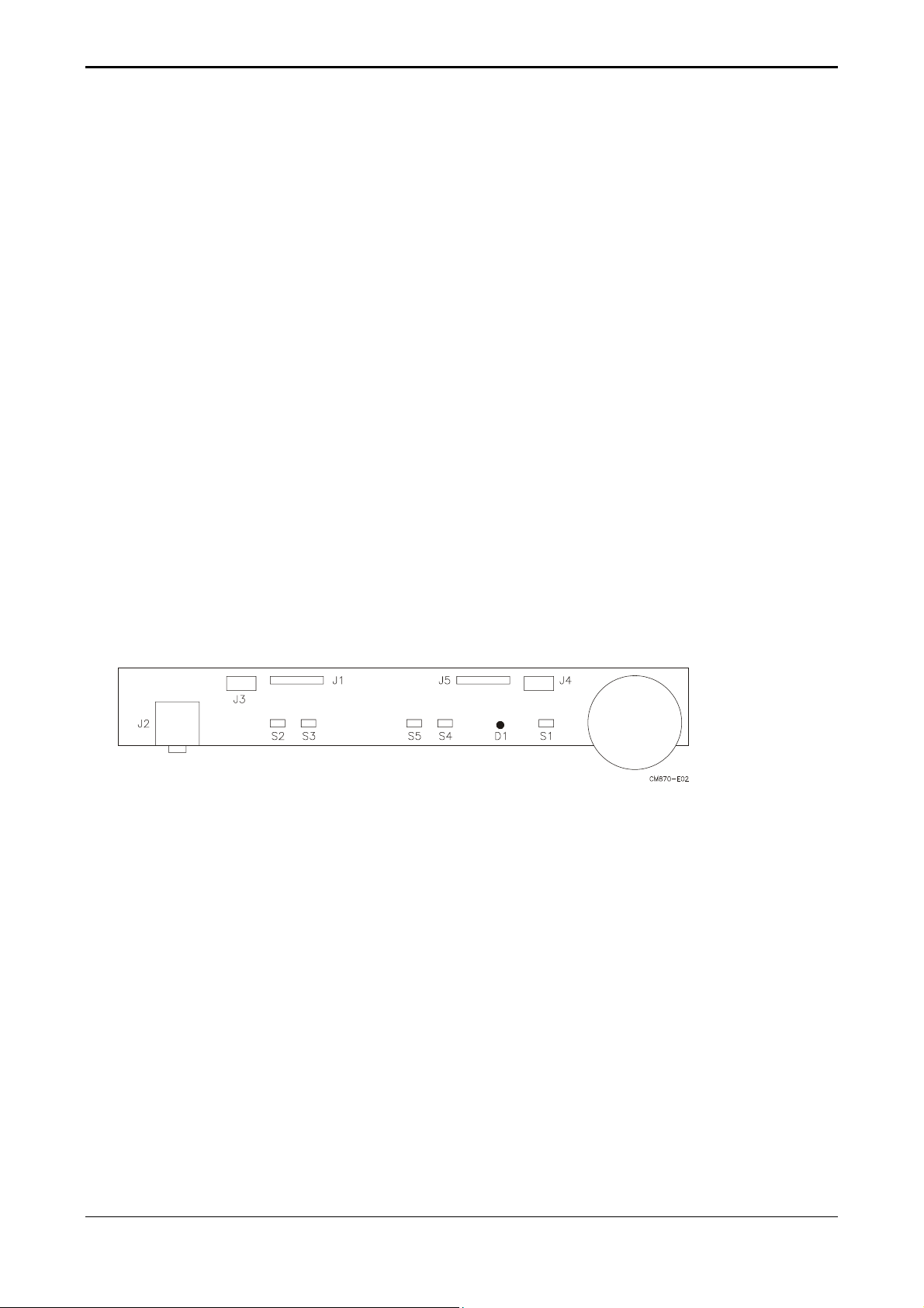
3. VK-515 Control Panel and Audio Board
A. Description
The VK-515 is designed to offer an user interfaced control panel which passes and receives
signals to and from VL-701 display control board. Also there is a stereo audio amplifier to
drive a pair of speakers .When in power saving mode the audio circuit can be turned off by the
control signal from VL-701 board.
B. Connector and Switch Locations
C. Connector type
Location Type Maker Number of pins
J1 96113-0813 E&T 8
J2 SCJ-0348-C SC 9
J3 87502-0200 ACES 2
J4 87502-0200 ACES 2
J5 96113-1013 E&T 10
7
Page 14

D. Connector pin Assignment
D-1 J1
Pin NO. Signal Comment
1 VOL Audio Volume Adjust
2,5,8 GND GND
3 OUTL - Left side audio signal
4 OUTL + Left side audio signal
6 OUTL - Right side audio signal
7 OUTL + Right side audio signal
D-2 J5
Pin NO. Signal Comment
1 MUTE Volume adjust power input.
2 LED-Y Power saving mode.
3 LED-G Monitor on mode.
4,10 GND
5 KEY-UP Function select up to VL-701
6 KEY-DOWN Function select down to VL-701
7 KEY-R Function select right to VL-701
8 KEY-L Function select left to VL-701
9 KEY-PWR Power ON/OFF signal to VL-701
D-3 J3 and J4
Pin NO. Signal Comment
1 LO (RO) Speaker out
2 OUTL - (OUTR-) Speaker out
D-4 J2
Pin NO. Signal I/O Comment
1 GND Ground
2 LI 2 Earphone out L
3 RI 2 Earphone out R
4 LI 1 Earphone out L
5 LO Speaker out L
6 NC No connector
7 RI 1 Earphone out R
8 RO Speaker out R
8
Page 15

D-5 Switch definition
Location Definition
S1 Power ON/OFF
S2 Function select by clockwise direction
S3 Function select by counter-clockwise direction
S4 Adjust up
S5 Adjust down
D-6 LED definition
Location Definition
D1 Green for ON mode; Dark for DC power off; Yellow for stand by; suspend;
off mode.
D-7 Variable resistor
VR1:Volume control, clockwise for increasing; counter-clockwise for decreasing
°°°°
D-8 Electrical characteristics (Tamb=25
)
Audio amplifier (Use Panasonic VP-7723A Audio Analyzor).
Item Audio Input Freq. Spec. Comment
Min. Typ. Max.
Input Voltage(V) 11.4 12 12.6
Input Current(mA) 500 800
Audio Voltage Gain 500mVrms 1KHz 14dB
Frequency Response 100mVrms 50Hz~20KHz -3dB +3dB
Signaal to Noise ratio 500mVrms 1KHz -70dB
Cross talk 100mVrms 1KHz -60dB
Distortion 500mVrms 1KHz 1%
Output Watt. 500mVrms 1KHz 0.5W
Volume Control Analog
Volume Max.,load 8 Ω
Volume Max.,load 8 Ω
Volume Max.,load 8 Ω
Volume Max.,load 8 Ω
Volume Max.,load 8 Ω
Volume Max.,load 8 Ω
9
Page 16

4. VM-515 POWER and AUDIO
A. Major Specification
Input voltage: 12V±5% from adapter (LSE 9901B1260)
Inout current: 5A max.
Output:
ITEM Output Voltage
VCC +5.1V 1.9A 0.19A
Max Load. Min Load Tolerance Ripple & Noise(max)
±5%
150mVpp
B. Description
The VM-515 is designed to supply the power to the VL-701 display control board. Under the
control of VL-701, it can run into power saving mode so that saving the power of the whole
monitor.
C. Efficiency:
80%min. at Maximum Load.
D. Connector Locations
10
Page 17

E. Connector type
Location Type Maker Number of pins
J801 DC-IN SC 2
J802 B4B-XH-A JST 4
J2 96113-0803 E&T 8
J3 SCJ-0345-1-X-S SCJ 3
F. Connector pin Assignment
F-1 J801 DC 12V Input
Pin No Signal Comment
Pin 1 +12V From adapter output cable
Pin 2 GND From adapter output cable
F-2 J802 FOR I/F CKT
Pin No Signal Comment
Pin 1 +12V From adapter +12V power
Pin 2 +5.1V Supply for I/F CKT
Pin 3, 4 GND GND
F-3 J2 FOR K/B SPEAKER
Pin No Signal Comment
Pin 1 VoL Adjustment audio volume.
Pin 2, 5, 8 GND GND
Pin 3 OUTL - Audio output L -
Pin 4 OUTL + Audio output L +
Pin 6 OUTR - Audio output R -
Pin 7 OUTR + Audio output R +
F-4 J3 AUDIO INPUT
Pin No Signal Comment
Pin 1 GND GND
Pin 2 IN-R Audio input R
Pin 3 IN-L Audio input L
11
Page 18

5. PK07006700/AMBIT T51I036.00 INVERTER BOARD
A. Description
The T51I036.00 Inverter board is designed for lighting up the back-lights of LCD module.
B. Electrical characteristics (FOR SAMSUNG PANEL/LT170E2-131)
MIN. TYP. MAX. COMMENT
INPUT VOLTAGE 11.4V 12V 12.6V
INPUT CURRENT -------- 2A --------
12V±5%
Vin=12V MAX.
BRIGHTNESS
Vbrite=0V
NO LOAD BACKLIGHT
VOLTAGE
LAMP CURRENT 6.2mA 13mA rms. 13.6mArms
DRIVING FREQUENCY 40KHz -------- 60KHz
EFFICIENCY -------- 78% -------- Vin = 12V,max brightness
Operating Life Time 20,000 ------- -------- Hours (note)
PWM dimming frequency 120HZ 140HZ 160HZ.
Brightness range
Vbrite 0V -------- 5V
-------- 690V rms. --------
170cd/ 200cd/
--------
0V, brightness max
Vin On/ OFF sequence -------- 0.5Sec --------
OLP Time -------- 1Sec -------- Open Lamp protection time
Duty control 20%
Strike voltage at 0° C
Strike voltage at 25° C
-------- --------
-------- --------
--------
100%
1420Vrms
1100Vrms
Note:
Life time(Hr) can be defined as the time in which it continues to operate under the
condition:
Ta=25±2°C, I
=13.0mArms until one of the following event occurs:
L
1. When the brightness becomes 50% above
2. When the startup voltage (Vs) at 0°C becomes higher than the maximal value of Vs
specified above
12
Page 19

C. Connector locations
D. Connector pin Assignment
D-1 CN1(ACES, 85205-1200 12P)
Pin NO. Signal Comment
1,2,3 BP+ +12V
5,6,10,11,12 GND GND
4 BLT_ON Back-light ON/OFF control , high active(5V)
7 +5VS +5VS
9 BRITE BRITE Brightness (0-5V)control from I/F
0V for max. brightness
8 NC NC
D-2 CN2,CN3 (JST SM04(4.0)B-BHS-14P)
Pin NO. Signal Comment
1 HV High voltage for lamp
2 HV High voltage for lamp
3 NC NC
4 LV Low voltage (common)
13
Page 20

6. AC Adapter(LSE9901B1260)
A-1 Quick specification review
• Input voltage
Single phase, 50/60HZ, 100VAC to 240VAC ±10%
• Input current
1.5A (max), at 90VAC input and full load 0.75A (max), at 264 VAC input and full
load.
• Inrush current @ cold start
30A(0-peak)@ 110Vac ,50A(0-peak) @ 220Vac
• Output
Tolerance Output Current
Output Volt - MIN MAX
+12Vdc
±5%
0A 5A 11.4~12.6Vdc
• Total output power: 60 Watt max.
• Efficiency
80% min. @115V/230VAC, maximum load.
• Dimension: 110Lx63Wx31H
7. CIRCUIT DESCRPTION
A. Display-Controller
The U12 is image processor. The functions of the CHIP support as below:
1. Hight quality image scalar
2. On-Chip 16 bit Microprocessor
3. On screen display
4. Automatic image optimizer
Volt Tolerance
B. Circuit of Plug and Play
Plug and play allows the serial communication of host PC and peripherals offering minimal
configurations to end users. This monitor supports DDC2B communication protocal.
C. System Clock
The U15(130MHz)&U16(96 MHz) support U12 reference clock.
D. Power Regulator
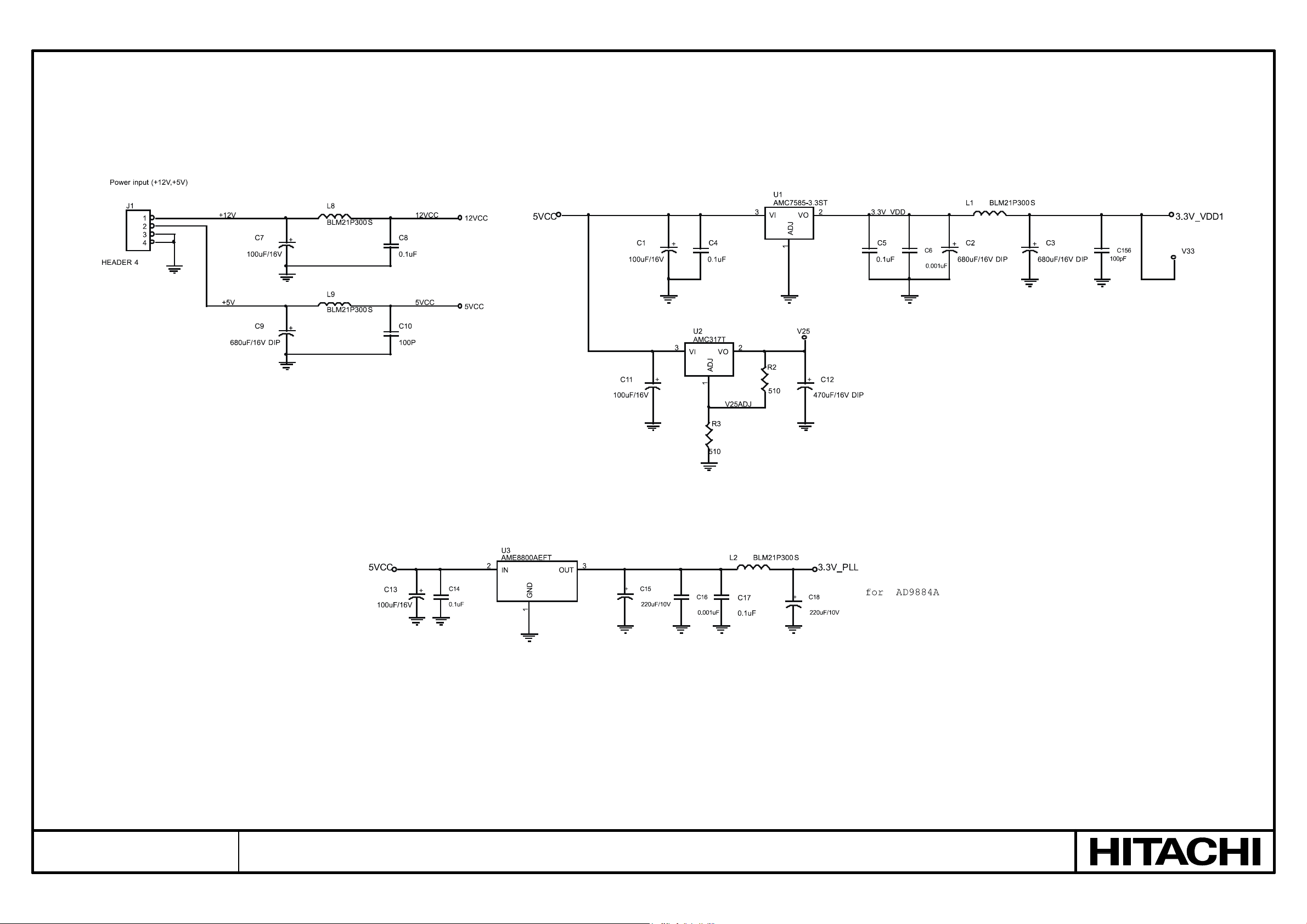
1. The U1 (AMC7585) & U3(AME 8800)are linear requlator that transfer input voltage from
5V to 3.3V.
2. The U2 (AMC317T) is linear requlator that transfer input voltage from 5V to 2.5V.
14
Page 21

8. Introduction
A. Front Panel Control and Led
Front Panel Controls
Item Control Function
1 Power Switch Turns the monitor on and off.
2 Power LED 1. Green indicates monitor is turns on.
2. Dark indicates DC power off.
3. Yellow indicates stand-by, suspend, off mode.
3
Function Button Launches OSD function menu circully
4
5 Plus Button Selects and adjusts the functions
6 Minus Button Selects and adjusts the functions
15
Page 22

B. Rear Panel connector Input Signals
Rear Panel Cable and Connector
Item Cable / Connector Function
1
2
3
Signal Connector Connectors the video cable
Power Connector
Audio connector Connector the audio cable
Connectors the adapter cable
16
Page 23

9. TROUBLESHOOTING
A. Main Procedure
17
Page 24

A-1 Power Circuit Troubleshooting
18
Page 25

A-2 Backlights Troubleshooting
19
Page 26

A-3 Performance Troubleshooting
20
Page 27

A-4 Function Troubleshooting
21
Page 28

SCHEMATIC CIRCUITS
Page 29
No. 0504
Control Board VL-701
Page 30

No. 0504
Control Board VL-701
Page 31

No. 0504
Control Board VL-701
Page 32

No. 0504
Control Board VL-701
Page 33

No. 0504
Control Board VL-701
Page 34

No. 0504
Control Board VL-701
Page 35

No. 0504
Control Board VL-701
Page 36

No. 0504
Control Panel VK-515
Page 37

No. 0504
Power & Audio Board VM-515
Page 38

No. 0504
Power & Audio Board VM-515
Page 39

No. 0504
Power & Audio Board VM-515
Page 40

THE UPDATED PARTS LIST
FOR THIS MODEL IS
AVAILABLE ON ESTA
Page 41

Hitachi, Ltd. Tokyo, Japan
International Sales Division
THE HITACHI ATAGO BUILDING,
No. 15 –12 Nishi Shinbashi, 2 – Chome,
Minato – Ku, Tokyo 105-8430, Japan.
Tel: 03 35022111
HITACHI EUROPE LTD,
Whitebrook Park
Lower Cookham Road
Maidenhead
Berkshire
SL6 8YA
UNITED KINGDOM
Tel: 01628 643000
Fax: 01628 643400
Email: consumer-service@hitachi-eu.com
HITACHI EUROPE GmbH
Munich Office
Dornacher Strasse 3
D-85622 Feldkirchen bei München
GERMANY
Tel: +49-89-991 80-0
Fax: +49-89-991 80-224
Hotline: +49-180-551 25 51 (12ct/min)
Email: HSE-DUS.service@hitachi-eu.com
HITACHI EUROPE srl
Via Tommaso Gulli N.39, 20147
Milano, Italia
ITALY
Tel: +39 02 487861
Tel: +39 02 38073415 Servizio Clienti
Fax: +39 02 48786381/2
Email: customerservice.italy@hitachi-eu.com
HITACHI EUROPE S.A.S
Lyon Office
B.P. 45, 69671 BRON CEDEX
FRANCE
Tel: 04 72 14 29 70
Fax: 04 72 14 29 99
Email: france.consommateur@hitachi-eu.com
HITACH EUROPE AB
Egebækgård
Egebækvej 98
DK-2850 Nærum
DENMARK
Tel: +45 43 43 6050
Fax: +45 43 60 51
Email: csgnor@hitachi-eu.com
Hitachi Europe Ltd
Bergensesteenweg 421
1600 Sint- Pieters-Leeuw
BELGIUM
Tel: +32 2 363 99 01
Fax: +32 2 363 99 00
Email: sofie.van.bom@hitachi-eu.com
www.hitachidigitalmedia.com
HITACHI EUROPE S.A.
364 Kifissias Ave. & 1, Delfon Str.
152 33 Chalandri
Athens
GREECE
Tel: 1-6837200
Fax: 1-6835964
Email: service.hellas@hitachi-eu.com
HITACHI EUROPE S.A.
Gran Via Carlos III, 101- 1
08028 Barcelona
SPAIN
Tel: 93 409 2550
Fax: 93 491 3513
Email: atencion.cliente@hitachi-eu.com
HITACHI Europe AB
Box 77 S-164 94 Kista
SWEDEN
Tel: +46 (0) 8 562 711 00
Fax: +46 (0) 8 562 711 13
Email: csgswe@hitachi-eu.com
HITACHI EUROPE LTD (Norway) AB
STRANDVEIEN 18
1366 Lysaker
NORWAY
Tel: 67 5190 30
Fax: 67 5190 32
Email: csgnor@hitachi-eu.com
HITACHI EUROPE AB
Neopoli / Niemenkatu 73
FIN-15140 Lahti
FINLAND
Tel : +358 3 8858 271
Fax: +358 3 8858 272
Email: csgnor@hitachi-eu.com
HITACHI EUROPE LTD
Na Sychrove 975/8
101 27 Praha 10 – Bohdalec
CZECH REPUBLIC
Tel: +420 267 212 383
Fax: +420 267 212 385
Email: csgnor@hitachi-eu.com
 Loading...