

Page 1
SERVICE MANUAL
MANUEL D'ENTRETIEN
WARTUNGSHANDBUCH
CAUTION:
Before servicing this chassis, it is important that the service technician read the “Safety
Precautions” and “Product Safety Notices” in this service manual.
No. 0421
«MODEL NAMES»
CML156XW
CML158XW
Data contained within this Service
manual is subject to alteration for
improvement.
ATTENTION:
Avant d’effectuer l’entretien du châassis, le technicien doit lire les «Précautions de sécurité»
et les «Notices de sécurité du produit» présentés dans le présent manuel.
VORSICHT:
Vor Öffnen des Gehäuses hat der Service-Ingenieur die „Sicherheitshinweise“ und „Hinweise
zur Produktsicherheit“ in diesem Wartungshandbuch zu lesen.
Les données fournies dans le présent
manuel d’entretien peuvent faire l’objet
de modifications en vue de perfectionner
le produit.
Die in diesem Wartungshandbuch
enthaltenen Spezifikationen können sich
zwecks Verbesserungen ändern.
SPECIFICATIONS AND PARTS ARE SUBJECT TO CHANGE FOR IMPROVEMENT
LCD Colour Monitor
November 2003
Page 2

SAFETY PRECAUTIONS
WARNING: The following precautions must be observed.
ALL PRODUCTS
Before any service is performed on the chassis an
isolation transformer should be inserted between the
power line and the product.
1. When replacing the chassis in the cabinet, ensure
all the protective devices are put back in place.
2. When service is required, observe the original
lead dressing. Extra precaution should be taken to
ensure correct lead dressing in any high voltage
circuitry area.
3. Many electrical and mechanical parts in
HITACHI products have special safety related
characteristics. These characteristics are often not
evident from visual inspection, nor can the
protection afforded by them necessarily be
obtained by using replacement components rated
for higher voltage, wattage, etc. Replacement
parts which have these special safety
characteristics are identified by marking with a
! on the schematics and the replacement parts
list.
The use of a substitute replacement component
that does not have the same safety characteristics
as the HITACHI recommended replacement one,
shown in the parts list, may create electrical
shock, fire, X-radiation, or other hazards.
4. Always replace original spacers and maintain lead
lengths. Furthermore, where a short circuit has
occurred, replace those components that indicate
evidence of overheating.
5. Insulation resistance should not be less than 2M
ohms at 500V DC between the main poles and
any accessible metal parts.
6. No flashover or breakdown should occur during
the dielectric strength test, applying 3kV AC or
4.25kV DC for two seconds between the main
poles and accessible metal parts.
7. Before returning a serviced product to the
customer, the service technician must thoroughly
test the unit to be certain that it is completely safe
to operate without danger of electrical shock. The
service technician must make sure that no
protective device built into the instrument by the
manufacturer has become defective, or
inadvertently damaged during servicing.
CE MARK
1. HITACHI products may contain the CE mark on
the rating plate indicating that the product
contains parts that have been specifically
approved to provide electromagnetic
compatibility to designated levels.
2. When replacing any part in this product, please
use only the correct part itemised in the parts list
to ensure this standard is maintained, and take
care to replace lead dressing to its original state,
as this can have a bearing on the electromagnetic
radiation/immunity.
PICTURE TUBE
1. The line output stage can develop voltages in
excess of 25kV; if the E.H.T. cap is required to be
removed, discharge the anode to chassis via a
high value resistor, prior to its removal from the
picture tube.
2. High voltage should always be kept at the rated
value of the chassis and no higher. Operating at
higher voltages may cause a failure of the picture
tube or high voltage supply, and also, under
certain circumstances could produce X-radiation
levels moderately in excess of design levels. The
high voltage must not, under any circumstances,
exceed 29kV on the chassis (except for projection
Televisions).
3. The primary source of X-radiation in the product
is the picture tube. The picture tube utilised for
the above mentioned function in this chassis is
specially constructed to limit X-radiation. For
continued X-radiation protection, replace tube
with the same type as the original HITACHI
approved type
4. Keep the picture tube away from the body while
handling. Do not install, remove, or handle the
picture tube in any manner unless shatterproof
goggles are worn. People not so equipped should
be kept away while picture tubes are handled
LASERS
If the product contains a laser avoid direct exposure to
the beam when the cover is open or when interlocks are
defeated or have failed.
Page 3

1. ELECTRICAL REQUIREMENTS
1.1 LCD Panel Specification ...................................................................................................................... 2
1.2 Input Signals ........................................................................................................................................ 7
1.3 Supported Timing ................................................................................................................................ 8
1.4 Power Management............................................................................................................................. 9
1.5 Plug & Play .......................................................................................................................................... 9
1.6 External Connection ............................................................................................................................ 9
2. ADJUSTMENT OF POWER SUPPLY
3. VL-563 DISPLAY CONTROL BOARD
3.1 Description......................................................................................................................................... 11
3.2 Features............................................................................................................................................. 11
3.3 BLOCK DIAGRAM............................................................................................................................. 12
3.4 Connector Locations.......................................................................................................................... 12
3.5 Connector Type ................................................................................................................................. 13
3.6 Connector pin assignment ................................................................................................................. 13
4. VK-580 CONTROL PANEL AND AUDIO BOARD
(CML158XW)
4.1 Description......................................................................................................................................... 16
4.2 Electrical characteristics (Tamb=25°)................................................................................................ 16
4.3 Connector type .................................................................................................................................. 16
4.4 Connector pin Assignment ................................................................................................................ 17
4.5 Switch definition................................................................................................................................. 18
4.6 LED definition .................................................................................................................................... 18
4.7 Variable resistor................................................................................................................................. 18
5. VK-570 CONTROL PANEL (CML156XW)
5.1 Description......................................................................................................................................... 19
5.2 Connector pin Assignment ................................................................................................................ 19
5.3 Switch definition................................................................................................................................. 19
5.4 LED definition .................................................................................................................................... 19
6. VP-570 POWER BOARD
6.1 Description......................................................................................................................................... 20
6.2 Features............................................................................................................................................. 20
6.3 Interface Signals ................................................................................................................................ 20
6.4 Electrical Specification:...................................................................................................................... 21
6.5 Isolation Check .................................................................................................................................. 23
6.6 Environmental.................................................................................................................................... 24
7. INTRODUCTION
7.1 Front Panel Control and Led.............................................................................................................. 25
7.2 Rear Panel connector Input Signals .................................................................................................. 27
8. TROUBLESHOOTING
8.1 Main Procedure ................................................................................................................................. 28
APPENDIX A: DISPLAY UNIT ASSEMBLY......................................................................33
1
Page 4

1. ELECTRICAL REQUIREMENTS
1.1 LCD Panel Specification
1.1.1 LCD Panel Model (HSD150SX84-C)
• Display Type Active matrix colour TFT LCD
• Resolution 1024 x 768 pixels
• Display Dot 1024 x (RGB) x 768
• Display Area 304.1mm (H) x 228.1mm (V)
• Pixel Pitch 0.297mm (H) x 0.297mm (V)
• Display Colour 262,144
(Monitor display colour 16.7M
with FRC or dithering)
• Maximum Brightness 250 cd/m
(6mA for each lamp after 30 min.)
• Contrast Ratio 400:1 typ.
• Response Time (Tr+Tf) 35ms typ
• Lamp Voltage 660Vrms typ.
• Lamp Current 3~7mA rms. typ. x 2 (Lamp)
• View Angle (Hor./Ver.) 65°(L), 65°(R) / 45°(H), 55°(L). typ.
• Uniformity =(Bmin/Bmax)x100% 70% min.
Bmax: Maximum Brightness
Bmin: Minimum Brightness
• Weight 950g. typ.
2
typ.
(Contrast Ratio ≥ 10)
2
Page 5
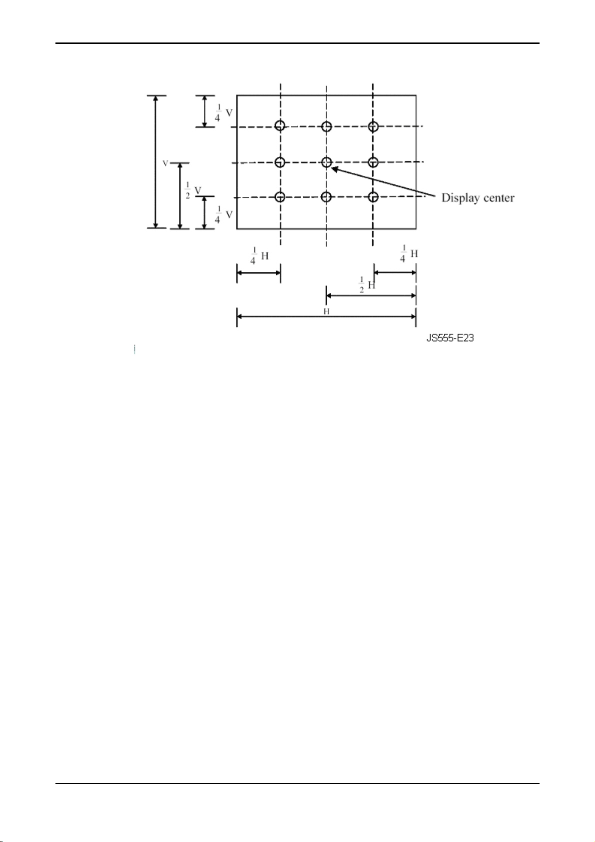
1.1.2 Optical Characteristics
Measuring Condition
■ Measuring surroundings : dark room
■ Lamp current I
■ V
■ Surrounding temperature : 25 ±2°C
■ 30min. Warm-up time.
=3.3V, fv =60Hz, f
DD1
Measuring Equipment
■ LCD-7000 (Otsuka Electric Corp.) utilises MCPD-7000 for Chromaticity and BM-5A for
other optical characteristics.
■ Measuring spot size : 10~12mm
Optical Specification
: (6.0) ±0.1mA, Lamp freq. FL =50KHz
BL
=32.5MHz
DCLK
3
JS555-E26
Page 6
Note (1) Definition of Viewing Angle:
Note (2) Definition of Contrast Ratio (CR):
Measured at the centre point of panel
Luminance with all pixels white (L63)
CR = ———————————————
Luminance with all pixels white (L0)
4
Page 7
Note (3) Definition of Response Time: Sum of TR and TF
Note (4) Optical Characteristic Measurement Setup
5
Page 8
Note (5) Definition of Brightness Uniformity
6
Page 9

1.2 Input Signals
1.2.1 Video Input
• Type Analog RGB.
• Input Impedance 75 ohm ± 2%
• Polarity Positive
• Amplitude 0 - 0.7 ± 0.05 Vp-p
• Display Colour same as LCD panel
1.2.2 Sync Input
• Signal separate horizontal and vertical sync.
• Polarity positive and negative.
1.2.3 Interface Frequency
which are TTL compatible, composite sync(H+V)
The following frequency range is generalised by supported timing. If the entered
mode does not match the supported timing the display optimisation will not be
assured.
• Horizontal Frequency 24KHz ---61KHz
• Vertical Frequency 49Hz -------75Hz
7
Page 10
1.3 Supported Timing
TIMING FH(KHZ)
FV(HZ)
31.469 + 800 640 96 16 48 25.175 640x350
VGA-350
NEC PC9801
VGA-GRAPH
NEC PC9821
VGA-480
VESA-480-72Hz
VESA-480-75Hz
VGA-400-TEXT
SVGA
VESA-600-60Hz
VESA-600-72Hz
VESA-600-75Hz
XGA
COMPAQ-XGA
VESA-768-70Hz
VESA-768-75Hz
APPLE MAC-800
VESA-PAL
70.087 − 449 350 2 37 60
24.83 − 848 640 64 64 80 21.05 640x400
56.42 − 440 400 8 7 25
31.469 − 800 640 96 16 48 25.175 640x400
70.087 + 449 400 2 12 35
31.5 − 800 640 64 16 80 25.197 640x400
70.15 − 449 400 2 13 34
31.469 − 800 640 96 16 48 25.175 640x480
59.94 − 525 480 2 10 33
37.861 − 832 640 40 24 128 31.5 640x480
72.809 − 520 480 3 9 28
37.5 − 840 640 64 16 120 31.5 640x480
75 − 500 480 3 1 16
31.469 − 900 720 108 18 54 28.322 720x400
70.087 + 449 400 2 12 35
35.156 + 1024 800 72 24 128 36 800x600
56.25 + 625 600 2 1 22
37.879 + 1056 800 128 40 88 40 800x600
60.317 + 628 600 4 1 23
48.077 + 1040 800 120 56 64 50 800x600
72.188 + 666 600 6 37 23
46.875 + 1056 800 80 16 160 49.5 800x600
75 + 625 600 3 1 21
48.363 − 1344 1024 136 24 160 65 1024x768
60.004 − 806 768 6 3 29
53.964 + 1328 1024 176 16 112 71.664 1024x768
66.132 + 816 768 4 8 36
56.476 − 1328 1024 136 24 144 75 1024x768
70.069 − 806 768 6 3 29
60.023 + 1312 1024 96 16 176 78.75 1024x768
75.029 + 800 768 3 1 28
49.725 - 1152 832 64 32 224 57.2832 832x624
74.55 - 667 624 3 1 39
31.469 - 800 640 96 16 48 25.175 640X480
50.030 - 629 480 2 62 85
SYNC
POLARITY
TOTAL
(DOT/LINE)
ACTIVE
(DOT/LINE)
SYNC
WIDTH
(DOT/LINE)
FRONT
PORCH
(DOT/LINE)
BACK
PORCH
(DOT/LINE)
PIXEL
FREQUENCY
(MHZ)
Note1: Mode 640x350, 640x400 and 720x400 cannot be expanded to full screen in vertical direction.
Note 2: Below 800x600 (i.e. 640x??? and 720x???), modes do not support NTAA (No Touch Auto-Adjustment)
8
Page 11
1.4 Power Management
1. Meets VESA DPMS Proposal
2. Power Consumption
Meets VESA DPMS Proposal
On mode 30 Wmax Green
Stand-by 3 Wmax Amber
Suspend 3 Wmax Amber
Off mode 3 Wmax Amber
DC power off 3 Wmax Dark
disconnection 3 Wmax
Measured from AC input end of AC power and do not include audio at power-saving state
The stand-by, suspend and off mode recover to on-mode in about 3 seconds.
1.5 Plug & Play
(supports VESA DDC1 and DDC2B functions)
1. Amber (stand-by; suspend; off-mode)
2. Dark (DC power off)
1.6 External Connection
1.6.1 AC Inlet (Rich-Bay R-30190)
1.6.2 Signal Connector (13 pin D-sub connector)
Pin assignment:
Pin NO. Signal
1 Vertical Sync
2 Horizontal Sync
3 Blue Video Ground
4 Blue Video
5 Green Video Ground
6 Green Video
7 Red Video Ground
8 Red Video
9 Shield Ground
10 DDC-SCL
11 DDC-SDA
12 PC-DETECT
13 PC-5V
1.6.3 Video Cable
(1.5M, with 15 pin D-sub VGA connector)
9
Page 12
2. ADJUSTMENT of Power Supply
Input voltage AC 100 ~ 240Vac
Rated input voltage AC 90 ~ 264Vac
Frequency 50 / 60 Hz
Rated frequency 47 ~ 63 Hz
DC output
Out voltage +12V +5V
Maximum output current +1.5A +1.5A
Minimum output current 0A +0.1A
Range of voltage Regulation
+25%~-5% +5%~-3%
10
Page 13

3. VL-563 DISPLAY CONTROL BOARD
3.1 Description
The VL-563 display control board is designed to directly convert the analog RGB signals from
standard VGA display card to optimum LCD timing signals so as to construct a high display
quality LCD monitor.
3.2 Features
•
Support for image expansion and reduction.
• Fast and automatic optimisation of phase, H size, Vert & Horz Position.
• On board micro-processor to detect display timings and control user functions.
• Uses MRT design to generate optimum LCD timings.
• Uses EEPROM to memorise every adjusted parameter.
• Supports up to 16 display modes from VGA to XGA.
• Offers full screen expansion function on non-XGA mode (automatic).
• Flexible colour temperature selection function including 9300, 6500 and user mode.
• Supports OSD functions.
• Supports VESA DPMS function.
• Supports DDC1/2B functions.
• Supports 8 languages for OSD description.
• The longest time for mode change is 3 seconds.
11
Page 14

3.3 BLOCK DIAGRAM
3.3.1 System Block Diagram
3.4 Connector Locations
12
Page 15

3.5 Connector Type
Location Number of pins
CN6 6
CN4,CN5 40
CN2 8
CN9 10
CN1 13
CN8 2
CN7 3
3.6 Connector Pin Assignment
3.6.1 CN1
Pin NO. Signal Comment
1 VS Vertical Sync Input.
2 HS Horizontal Sync Input.
3 Ground Ground.
4 B-Video Blue Video Input.
5 Ground Ground.
6 G-Video Green Video Input.
7 Ground Ground
8 R-Video Red Video Input.
9 Ground Ground.
10 SCL DDC 2B
11 SDA DDC 1/2B
12 PCDETECT PCDETECT Input.
13 5VCC DDC Power Input.
13
Page 16

3.6.2 CN4/CN5
I/O CONNECTION PIN ASSIGNMENT - Interface FPC Connector (40-pins x 2)
(JAE:FH1B040H52)
I/F FRC Connector (J1) CN4 I/F FRC Connector (J2) CN5
Pin Symbol Description Pin. Symbol Description
1 NC No Connecting 1 VDD Digital Power Input (DC+3.3V)
2 NC No Connecting 2 VDD Digital Power Input (DC+3.3V)
3 GND Ground 3 GND Ground
4 GND Ground 4 GND Ground
5 EB5 Even-dot Blue Data bit 5 (MSB) 5 OB5 Odd-dot Blue Data bit 5 (MSB)
6 EB4 Even-dot Blue Data bit 4 6 OB4 Odd-dot Blue Data bit 4
7 EB3 Even-dot Blue Data bit 3 7 OB3 Odd-dot Blue Data bit 3
8 EB2 Even-dot Blue Data bit 2 8 OB2 Odd-dot Blue Data bit 2
9 EB1 Even-dot Blue Data bit 1 9 OB1 Odd-dot Blue Data bit 1
10 EB0 Even-dot Blue Data bit 0 (LSB) 10 OB0 Odd-dot Blue Data bit 0 (LSB)
11 GND Ground 11 GND Ground
12 EG5 Even-dot Green Data bit 5 (MSB) 12 OG5 Odd-dot Green Data bit 5 (MSB)
13 EG4 Even-dot Green Data bit 4 13 OG4 Odd-dot Green Data bit 4
14 EG3 Even-dot Green Data bit 3 14 OG3 Odd-dot Green Data bit 3
15 EG2 Even-dot Green Data bit 2 15 OG2 Odd-dot Green Data bit 2
16 EG1 Even-dot Green Data bit 1 16 OG1 Odd-dot Green Data bit 1
17 EG0 Even-dot Green Data bit 0 (LSB) 17 OG0 Odd-dot Green Data bit 0 (LSB)
18 GND Ground 18 GND Ground
19 ER5 Even-dot Red Data bit 5 (MSB) 19 OR5 Odd-dot Red Data bit 5 (MSB)
20 ER4 Even-dot Red Data bit 4 20 OR4 Odd-dot Red Data bit 4
21 ER3 Even-dot Red Data bit 3 21 OR3 Odd-dot Red Data bit 3
22 ER2 Even-dot Red Data bit 2 22 OR2 Odd-dot Red Data bit 2
23 ER1 Even-dot Red Data bit 1 23 OR1 Odd-dot Red Data bit 1
24 ER0 Even-dot Red Data bit 0 (LSB) 24 OR0 Odd-dot Red Data bit 0 (LSB)
25 GND Ground 25 GND Ground
26 CPH1 Pixel Clock Input 26 CPH2 Pixel Clock Input
27 GND Ground 27 GND Ground
28 GND Ground 28 GND Ground
29 STH Horizontal Start Pulse 29 NC No Connecting
30 LOAD Source Driver Latch Pulse 30 NC No Connecting
31 POL Source Driver Output Polarity control 31 NC No Connecting
32 REV Data Reverse Control Signal 32 NC No Connecting
33 GND Ground 33 NC No Connecting
34 GND Ground 34 NC No Connecting
35 STV1 Vertical Start Pulse1 35 NC No Connecting
36 STV2 Vertical Start Pulse2 36 NC No Connecting
37 CPV Vertical Clock Input 37 NC No Connecting
38 OE Gate Driver Output Enable Signal 38 NC No Connecting
39 GND Ground 39 GND Ground
40 GND Ground 40 GND Ground
14
Page 17

3.6.3 CN6
Pin No. Signal Comment
1 VCC(5V) Power Input
2 VCC(5V) Power Input
3 GND GND
4 GND GND
5 BLON Bright Light ON/OFF
6 BRIGHTNESS Brightness Adjustment
3.6.4 CN2
Pin NO. Signal Comment
1 KEY-R Function select clockwise key
2 LED-OR Power saving mode
3 LED-GRN Monitor is ON
4 GND GND
7 POWER Power ON/OFF key
8 KEY-L Function select anti-clockwise key
6 KEY-UP Adjust up key
5 KEY-DOWN Adjust down key
15
Page 18

4. VK-580 Control Panel and Audio Board (CML158XW)
4.1 Description
The VK-580 is designed to offer an user interfaced control panel which passes and receives
signals to and from VL-563 display control board. Also there is a stereo audio amplifier to drive
a pair of speakers. When in power saving mode the audio circuit can be turned off by the
control signal from VL-563 board.
4.2 Electrical Characteristics (Tamb=25 °°°°)
Audio amplifier (Use Panasonic VP-7723A Audio Analyzor).
Item Audio Input Freq. Spec. Comment
Min. Typ. Max.
Frequency
Response
Distortion 500mVrms 1KHz 2%
Output Watt. 500mVrms 1KHz 0.5W
Volume Control Analog
500mVrms 100Hz~20KHz -3dB +3dB
Volume Max., load 4Ω
Volume Max., load 4Ω
Volume Max., load 4 Ω
4.3 Connector Type
Location Number of pins
J1 10
J2 7
J3 2
J4 2
J5 8
Connector and Switch
Locations
16
Page 19

4.4 Connector Pin Assignment
4.4.1 J1
Pin NO. Comment
1 Audio out L+
2 Audio out L-
3 Audio out R-
4 Audio out R+
5 Audio volume adjust
6 VDD for audio volume adjust
7 GND
8 EAR phone out L
9 EAR phone out R
10 EAR phone Detector
4.4.2 J5
Pin NO. Signal Comment
1 KEY-R Function select clockwise key
2 LED-OR Power saving mode
3 LED-GRN Monitor is ON
4 GND GND
5 POWER Power ON/OFF key
6 KEY-L Function select anti-clockwise key
7 KEY-UP Adjust up key
8 KEY-DOWN Adjust down key
4.4.3 J3 and J4
Pin NO. Signal Comment
1 GND GND
2 OUTL (OUTR) Speaker out
17
Page 20

4.5 Switch Definition
Location Definition
S5 Power ON/OFF
S1 Function select by clockwise direction
S4 Function select by anti-clockwise direction
S3 Adjust up
S2 Adjust down
4.6 LED Definition
Location Definition
D1 Green for ON mode; Amber for power saving.
4.7 Variable Resistor
VR1: Volume control: clockwise for increasing, anti-clockwise for decreasing
18
Page 21

5. VK-570 Control Panel (CML156XW)
5.1 Description
The VK-570 is designed to offer an user interfaced control panel which passes and receives
signals to and from VL-563 display control board. When in power saving mode the audio
circuit can be turned off by the control signal from VL-563 board.
5.2 Connector Pin Assignment
5.2.1 J5
Pin NO. Signal Comment
3 KEY-R Function select clockwise key
4 LED-OR Power saving mode
3 LED-GRN Monitor is ON
4 GND GND
5 POWER Power ON/OFF key
6 KEY-L Function select anti-clockwise key
7 KEY-UP Adjust up key
8 KEY-DOWN Adjust down key
5.3 Switch Definition
Location Definition
S5 Power ON/OFF
S1 Function select by clockwise direction
S4 Function select by anti-clockwise direction
S3 Adjust up
S2 Adjust down
5.4 LED Definition
Location Definition
D1 Green for ON mode; Amber for power saving.
19
Page 22

6. VP-570 POWER Board
6.1 Description
This specification defines the performance and characteristic for the VP-570 power board. It
supplies the following items :
1) A constant 5V output source for logic board.
2) A constant 5V output source for audio power source.
2) A constant 12V output source for inverter power source.
6.2 Features
Wide input range : AC input 90 ~ 264Vrms
High efficiency : η>75%
Inverter brightness adjustment by continual mode
Protection function : DC output is design by auto-recovery.
It includes OPP, SCP.
6.3 Interface Signals
6.3.1 Input
1. AC Inlet: RICHBAY R-301-90
2. J701 :SCJ-0345-I-X-S SC 3Pin
6.3.2 Output
J801: The wire set of Pin2.0 /7Pin to Pin1.25/7 Pin , 110mm length
PIN NO. Function Function
1 +5V +5V supply for logic board
2 +5V +5V supply for logic board
3 GND Ground
4 GND Ground
5 VEN Enable signal for inverter (Low active , <1V)
6 VBRI Brightness signal for inverter (0V to 3.3V)
7 --
8 +5V +5V supply for audio’s power
9 GND Audio ground
J901 & J902: Inverter High Voltage Output
PIN NO. Function Comment
1 LV Low voltage (common)
2 HV High voltage for lamp
20
Page 23

t
6.4 Electrical Specification:
6.4.1 AC-DC Electrical Specification
6.4.1 Input Specification
No Item Condition Min. Typ. Max. Unit
1 Input Voltage
2 Input Frequency ----- 47 --- 63 Hz
3 Input Current 100Vac @ Type load 1.5A --- --- 1.0 Arms
Cold Start @ Vin=100Vrms --- 30 A
4 Inrush Current
Cold Start @ Vin=220Vrms
5 Hold Up Time
6 Turn on time Vin =110Vac --- 1.0 --- S
7 Efficiency +12V/1.5A ,+5Vcc/1.5A 70 --- --- %
8
Input Power
Consumption
@ full load & 100Vac input and Type
-----
load
Vin=220Vac --- --- 1.2 W
100 --- 240 Vac
---
--- 50 A
10 --- --- ms
0-P
0-P
*Cold start-up of Inrush Current : Power board off (keep over 1 hour) and Tamb=25degree C
6.4.1 AC-DC Output Specification
• Output
Tolerance Output Current
Output Voltage - MIN MAX
Voltage Tolerance
+5Vdc +5 /-3 % 0.05A 1.5A 4.85~5.25V dc
+12Vdc +25/-5 % 0A 1.5A 11.4~15Vdc
Ripple
Noise
Dynamic Load
Regulation
Over / Under
Shoo
1. Measured at DC output
terminals which are
paralleled with a 10uF
E-Cap & 0.1uF Ceramic
Cap.
2.Band width is limited
50~100% or 100~50%
load change of any DC
output @50% duty of
1MHz (min.)
@ Power line on/off ---
--- 1%
--- 3%
---
±5%
±5%
+5Vdc:50mVp-p
+12Vdc:120mVp-p
+5Vdc:150mVp-p
+12Vdc:360mVp-p
---
*+5Vcc load regulation test: +12V loading at 1.0A
*+12Vcc load regulation test: +5V loading at 1.0A
Protection Function: Auto-recovery design is acceptable but input power must
be less than 5W
21
Page 24

(
)
)
1)SCP: Short circuit protection must act on both outputs
2)OPP: Should be protected when output power consumption is within 40W ~ 70W
3)OCP:
Min. Max. Test condition
+5Vdc(for logic) 2A 6A +12V @1.5A
+12Vdc 1.8A
4.5 +5V(for logic) @1.5A
6.4.2
Inverter Electrical Specification:
For Hannstar HSD150SX84-B
Input Voltage --- --- 12 --- V
Condition
Min. Typ. Max. Unit
Input Current
Backlight ON/OFF Control
Brightness Adjust
Lamp Current Control
Output Voltage Vin=12V, Iout=6.5mA --- 750 --- Vrms
Brightness
Output Current(Each
connector
Frequency
Open Lamp Voltage --- 1350 --- --- Vrms
Striking Time --- --- 1.0 --- S
Lamp Current Balance --- --- ±0.3 --- mA
Efficiency Vin=12V --- 80 --- %
Min. Luminance / Max.
Luminance
--- --- 1.0 --- A
ON --- 0 --- V
OFF
HSD150SX84-B 200 250 ---
HSD150SX84-D 175 200 ---
Vbri=0V~3.3V 3 6.5 7 mA
--- 40 50 70 KHz
--- 3.0 --- V
--- 55% --- ---
Cd/m²
Operating Life Time --- 30000 --- --- Hr
*The open lamp voltage is tested at output connector terminal
*
Life time (Hr) can be defined as the time in which it continues to operate under the condition:
Ta=25±3°C, I
1. When the brightness becomes 50%
2. When the startup voltage (Vs) at 0°C becomes higher than the maximal value of Vs
=6.0Ma (ms) and fL=30 KHz until one of the following event occurs:
L
specified above
22
Page 25

6.4.3
Connector & Pin Assignment:
Output Connector:
J801 (for main board ) :
Pin No.
Symbol Description
1,2
3,4 GND Common Ground
5 Ven
6 Vbri
7 ---
8
9 GND
Vcc +5Vdc for main board
Backlight ON/OFF control, low active
Brightness adjustable range 0~3.3V
-----
Vaudio
+5Vdc for audio power
Audio ground
J901 & J902
Pin No.
Symbol Description
1
2 LV Low Voltage Output For Low Side CCFL
HV High Voltage Output For High Side CCFL
6.5 Isolation Check
6.5.1 Leakage Current: 0.25mA @ 100VAC
6.5.1 Insulation Resistance: more than 3M ohms while withstanding a voltage of 500VAC
6.5.1 Hi-Pot: 3KVAC using 3mA cut-off current
23
Page 26

6.6 Environmental
The PS shall be capable of withstanding the following
6.6.1 Temperature Range
Operating 0 to +40 degC
Storage -20 to +85 degC
6.6.2 Humidity
Operating 10 to 95% RH
Storage 10 to 95% RH
6.6.3 Altitude
Operating 0 to 10,000 feet
Non-Operating 0 to 25,000 feet
6.6.4 Vibration
Operating 1.0mm, 10-25Hz
15mm per cycle of each axis (XYZ)
Non-Operating: The power supply shall be designed to withstand normal transportation
vibration per MIL-STD-810D, method 514, procedure X.
24
Page 27

7. INTRODUCTION
7.1 Front Panel Control and LED
CML158XW (With Audio)
Front Panel Controls
Item Control Function
Figure 2-1
1
Stereo Speakers
Speaker Volume
2
Control
3
DC Power Switch
4
DC Power-On Indicator
Function Select
5
Buttons
Adjustment Control
6
Buttons
External Headphone
7
Jack
PC Audio Stereo output.
Increase Volume - Turn knob clockwise.
Decrease Volume - Turn knob anti-clockwise
Press the power switch to switch the monitor
ON/OFF.
LED lights Green color --- Power is ON.
LED lights Yellow --- Monitor is in "Power Saving
Mode".
LED is off --- Power is OFF.
Press either left or right control button for OSD (On
Screen Display) menu selection.
Press the left button to decrease the OSD setting
and press the right button to increase the OSD
setting.
The monitor speakers will be disabled when using
an external headphone or external speakers.
25
Page 28

CML156XW (Without Audio)
Front Panel Controls
Item Control Function
1 DC Power Switch
2 DC Power-On Indicator
3 Function Select Buttons
Adjustment Control
4
Buttons
Press the power switch to switch the monitor
ON/OFF.
LED lights Green color --- Power is ON.
LED lights Yellow --- Monitor is in "Power
Saving Mode".
LED is off --- Power is OFF.
Press either left or right control button for OSD
(On Screen Display) menu selection.
Press the left button to decrease the OSD setting
and press the right button to increase the OSD
setting.
26
Page 29

7.2 Rear Panel Connector Input Signals
Rear Panel Cable and Connector
Item Cable / Connector Function
1 Signal Cable Connect the video port
2 AC IN Power Connect Connect the AC power cord
Audio connector
3
(CML158XW
Only)
Connect the audio port
27
Page 30

8. TROUBLESHOOTING
8.1 Main Procedure
28
Page 31

8.1.1 Power Circuit Troubleshooting
29
Page 32

8.1.2 Backlights Troubleshooting
30
Page 33

8.1.3 Performance Troubleshooting
31
Page 34

8.1.4 Function Troubleshooting
32
Page 35

APPENDIX A
DISPLAY UNIT ASSEMBLY DIAGRAMS
CML158XW
CML156XW
33
Page 36

CML158XW
Display Unit Assembly
Page 37

CML156XW
Display Unit Assembly
Page 38

THE UPDATED PARTS LIST
FOR THIS MODEL IS
AVAILABLE ON ESTA
Page 39

Hitachi, Ltd. Tokyo, Japan
International Sales Division
THE HITACHI ATAGO BUILDING,
No. 15 –12 Nishi Shinbashi, 2 – Chome,
Minato – Ku, Tokyo 105-8430, Japan.
Tel: 03 35022111
HITACHI EUROPE LTD,
Whitebrook Park
Lower Cookham Road
Maidenhead
Berkshire
SL6 8YA
UNITED KINGDOM
Tel: 01628 643000
Fax: 01628 643400
Email: consumer-service@hitachi-eu.com
HITACHI EUROPE GmbH
Munich Office
Dornacher Strasse 3
D-85622 Feldkirchen bei München
GERMANY
Tel: +49-89-991 80-0
Fax: +49-89-991 80-224
Hotline: +49-180-551 25 51 (12ct/min)
Email: HSE-DUS.service@hitachi-eu.com
HITACHI EUROPE srl
Via Tommaso Gulli N.39, 20147
Milano, Italia
ITALY
Tel: +39 02 487861
Tel: +39 02 38073415 Servizio Clienti
Fax: +39 02 48786381/2
Email: customerservice.italy@hitachi-eu.com
HITACHI EUROPE S.A.S
Lyon Office
B.P. 45, 69671 BRON CEDEX
FRANCE
Tel: 04 72 14 29 70
Fax: 04 72 14 29 99
Email: france.consommateur@hitachi-eu.com
HITACH EUROPE AB
Egebækgård
Egebækvej 98
DK-2850 Nærum
DENMARK
Tel: +45 43 43 6050
Fax: +45 43 60 51
Email: csgnor@hitachi-eu.com
Hitachi Europe Ltd
Bergensesteenweg 421
1600 Sint-Pieters-Leeuw
BELGIUM
Tel: +32 2 363 99 01
Fax: +32 2 363 99 00
Email: sofie.van.bom@hitachi-eu.com
www.hitachidigitalmedia.com
HITACHI EUROPE S.A.
364 Kifissias Ave. & 1, Delfon Str.
152 33 Chalandri
Athens
GREECE
Tel: 1-6837200
Fax: 1-6835964
Email: service.hellas@hitachi-eu.com
HITACHI EUROPE S.A.
Gran Via Carlos III, 101-1
08028 Barcelona
SPAIN
Tel: 93 409 2550
Fax: 93 491 3513
Email: atencion.cliente@hitachi-eu.com
HITACHI HOME ELECTRONICS (NORDIC) AB
Box 77 S-164 94 Kista
SWEDEN
Tel: +46 (0) 8 562 711 00
Fax: +46 (0) 8 562 711 13
Email: csgswe@hitachi-eu.com
HITACHI EUROPE LTD (Norway) AB
STRANDVEIEN 18
1366 Lysaker
NORWAY
Tel: 67 5190 30
Fax: 67 5190 32
Email: csgnor@hitachi-eu.com
HITACHI EUROPE AB
Neopoli / Niemenkatu 73
FIN-15140 Lahti
FINLAND
Tel : +358 3 8858 271
Fax: +358 3 8858 272
Email: csgnor@hitachi-eu.com
HITACHI EUROPE LTD
Na Sychrove 975/8
101 27 Pr aha 10 – Bohdalec
CZECH REPUBLIC
Tel: +420 267 212 383
Fax: +420 267 212 385
Email: csgnor@hitachi-eu.com
 Loading...