

Page 1
SERVICE MANUAL
MANUEL D'ENTRETIEN
WARTUNGSHANDBUCH
CAUTION:
Before servicing this chassis, it is important that the service technician read the “Safety
Precautions” and “Product Safety Notices” in this service manual.
No. 0417
CML154XW
Data contained within this Service
manual is subject to alteration for
improvement.
ATTENTION:
Avant d’effectuer l’entretien du châassis, le technicien doit lire les «Précautions de sécurité»
et les «Notices de sécurité du produit» présentés dans le présent manuel.
VORSICHT:
Vor Öffnen des Gehäuses hat der Service-Ingenieur die „Sicherheitshinweise“ und „Hinweise
zur Produktsicherheit“ in diesem Wartungshandbuch zu lesen.
Les données fournies dans le présent
manuel d’entretien peuvent faire l’objet
de modifications en vue de perfectionner
le produit.
Die in diesem Wartungshandbuch
enthaltenen Spezifikationen können sich
zwecks Verbesserungen ändern.
SPECIFICATIONS AND PARTS ARE SUBJECT TO CHANGE FOR IMPROVEMENT
LCD Colour Monitor
November 2002
Page 2

1. 1. ELECTRICAL REQUIREMENTS................................................................................ 2
A. LCD Panel Specification............................................................................................................................ 2
B. CONTROLS ..............................................................................................................................................3
C. Power Management .................................................................................................................................. 3
D. Display Modes FOR Inspections ...............................................................................................................5
2. ADJUSTMENT CONDITIONS......................................................................................... 6
A. Measuring Apparatuses Used................................................................................................................... 6
B. Input Signal................................................................................................................................................6
C. Indication...................................................................................................................................................6
3. ADJUSTMENT OF POWER SUPPLY
...................................................................... 6
4. ADJUSTMENT OF BOARDS.......................................................................................... 7
A. Connection Method ................................................................................................................................... 7
5. DISPLAY CONTROL BOARD ........................................................................................ 9
A. Description.................................................................................................................................................9
B. Features .................................................................................................................................................... 9
C. Block Diagram (Control CKT).................................................................................................................. 10
D. Connector Locations................................................................................................................................11
E. Connector Type.......................................................................................................................................12
F. Connector pin assignment.......................................................................................................................12
6. VK-546 CONTROL PANEL BOARD............................................................................. 16
A. Description...............................................................................................................................................16
B. Connector and Switch Locations.............................................................................................................16
C. Connector type ........................................................................................................................................16
D. Connector pin Assignment ...................................................................................................................... 17
7. POWER BOARD........................................................................................................... 19
A. Description...............................................................................................................................................19
B. Electrical characteristics..........................................................................................................................19
C. Connector locations................................................................................................................................. 20
8. CIRCUIT DESCRPTION ............................................................................................... 21
A. Micro-Controller Circuit............................................................................................................................ 21
B. Circuit of Plug and Play ........................................................................................................................... 21
C. System Clock........................................................................................................................................... 21
D. Image Engine (Zoom).............................................................................................................................. 21
E. Power Regulator...................................................................................................................................... 21
9. INTRODUCTION........................................................................................................... 22
A. Front Panel Control and Led ................................................................................................................... 22
B. Rear Panel connector Input Signals......................................................................................................... 24
10. TROUBLESHOOTING............................................................................................. 25
A. Main Procedure....................................................................................................................................... 25
APPENDIX A: SCHEMATIC DIAGRAMS..........................................................................30
APPENDIX B: DISPLAY UNIT ASSEMBLY......................................................................36
APPENDIX C: PART LISTS ..............................................................................................37
1
Page 3
1. 1. ELECTRICAL REQUIREMENTS
A. LCD Panel Specification
Display: 15 inch (15” viewable image size): active matrix: thin film transistor
(TFT): liquid crystal display (LCD): 0.297 mm dot pitch: R.G.B.
Vertical stripe 200 cd//m
ratio, typical
2
white luminance, typical: 300:1 contrast
Compatibility:
Synchronization
Frequencies:
Resolution:
Active Display Area:
Viewing Angles:
640 x 350: VGA-350
720 x 400: VGA text
640 x 400: VGA-GRAPH
640 x 480: VGA, 60Hz to 75 Hz vertical refresh rate
800 x 600: 56Hz to 75 Hz vertical refresh rate
1024 x 768 non-interlaced: 60Hz to 75 Hz vertical refresh rate
Horizontal: 24 kHz to 60 kHz
Vertical: 56 Hz to 75 Hz (1024 x 768 is up to 75 Hz)
Pixel Frequency: 21 Mhz to 78 Mhz
Horizontal: 1024 dots
Vertical: 768 lines
Horizontal: 304.1 mm
Vertical: 228.1 mm
AU
Up 40deg down 60deg (TYP)
Hannstar
Up 45deg down 55deg (TYP)
Display Colors:
Power Supply:
Power
Consumption:
Environmental:
Left 60deg, Right 60deg (TYP)
CR > 10
6-bits driver
AC 100 to 240V worldwide input, 50 / 60Hz
Typical: 25W on mode +10 / -25%
Operating temperature: 0ºC to 50ºC
Storage temperature: -20ºC to 60ºC
Storage humidity: 10%~90%
Left 65deg, Right 65deg (TYP)
CR > 10
2
Page 4
B. CONTROLS
B-1 Control panel (monitor front panel)
1. Power LED, ( Please refer to C-2 LED definition table)
2. Adjust decrease.
3. Adjust increase
4. Function select counter-clockwise.
5. Function select clockwise.
6. Power ON/OFF switch, push to ON and push to OFF. (toggle switch)
C. Power Management
C-1 Power Management condition and status
State
On Pulses Pulses Active On On On Green
Stand-by No Pulses Pulses Blanking
Suspend Pulses No Pulses
Off No pulses No pulses Blacking On Yellow
DC Power off Don’t care Don’t care Don’t care Off Off
Horizontal Vertical Video Supply Circuit
Signals Power Video LCD LED
Off
Off
Off
Yellow
Off
3
Page 5
C-2 LED definition Table
State LED
On mode Green
Stand-by Yellow
Suspend Yellow
Off mode Yellow
power off Dark
disconnection
C-3 Power Consumption
Meet VESA DPMS Proposal
On mode 25 Wmax
Stand-by 5 Wmax
Suspend 5 Wmax
Off mode 5 Wmax
DC power off 5 Wmax
disconnection 5 Wmax
Measured from AC input, and not include audio at power-saving state
The stand-by, suspend and off mode recover to on mode about 3 seconds.
1. Yellow(stand-by; suspend; off mode)
2. LED Dark (power off)
4
Page 6
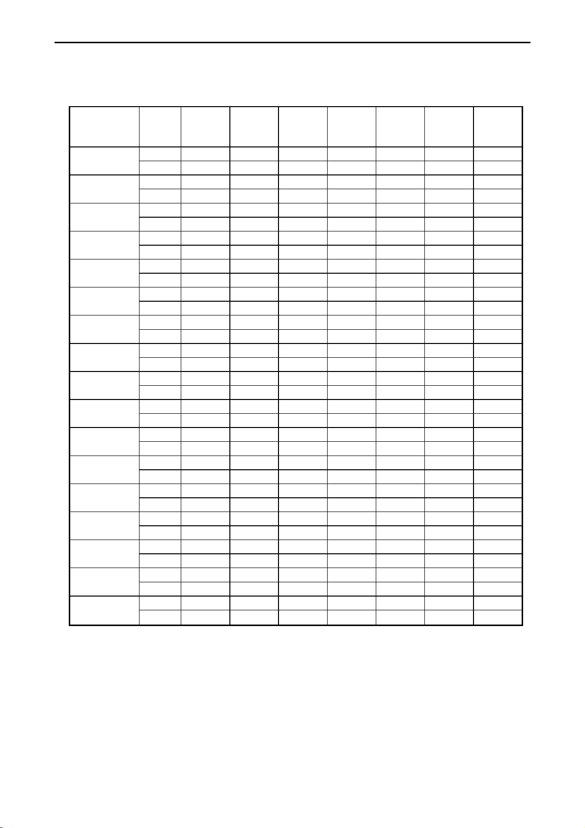
D. Display Modes FOR Inspections
D-1 Supported Timing(for Not supported timing will go to power saving mode)T
TIMING
640x350
VGA-350
640x400
NEC PC9801
640x400
VGA-GRAPH
640x400
NEC PC9821
640x480
VGA-480
640x480
VESA-480-72Hz
640x480
VESA-480-75Hz
720x400
VGA-400-TEXT
800x600
SVGA
800x600
VESA-600-60Hz
800x600
VESA-600-72Hz
800x600
VESA-600-75Hz
832x624
APPLE MAC-800
1024x768
XGA
1024x768
COMPAQ-XGA
1024x768
VESA-768-70Hz
1024x768
VESA-768-75Hz
FH(KHZ)
FV(HZ)
31.469
70.087
24.83
56.42
31.469
70.087
31.5
70.15
31.469
59.94
37.861
72.809
37.5
75
31.469
70.087
35.156
56.25
37.879
60.317
48.077
72.188
46.875
75
49.725 - 1152 832 64 32 224 57.2832
74.55 - 667 624 3 1 39
48.363
60.004
53.964
66.132
56.476
70.069
60.023
75.029
SYNC
POLARITY
+
−
−
−
−
+
−
−
−
−
−
−
−
−
−
+
+
+
+
+
+
+
+
+
−
−
+
+
−
−
+
+
TOTAL
(DOT/LINE)
800 640 96 16 48 25.175
449 350 2 37 60
848 640 64 64 80 21.05
440 400 8 7 25
800 640 96 16 48 25.175
449 400 2 12 35
800 640 64 16 80 25.197
449 400 2 13 34
800 640 96 16 48 25.175
525 480 2 10 33
832 640 40 16 120 31.5
520 480 3 1 20
840 640 64 16 120 31.5
500 480 3 1 16
900 720 108 18 54 28.322
449 400 2 12 35
1024 800 72 24 128 36
625 600 2 1 22
1056 800 128 40 88 40
628 600 4 1 23
1040 800 120 56 64 50
666 600 6 37 23
1056 800 80 16 160 49.5
625 600 3 1 21
1344 1024 136 24 160 65
806 768 6 3 29
1328 1024 176 16 112 71.664
816 768 4 8 36
1328 1024 136 24 144 75
806 768 6 3 29
1312 1024 96 16 176 78.75
800 768 3 1 28
ACTIVE
(DOT/LINE)
SYNC
WIDTH
(DOT/LINE)
FRONT
PORCH
(DOT/LINE)
BACK
PORCH
(DOT/LINE)
PIXEL
FOREQ.
(MHZ)
5
Page 7
2. ADJUSTMENT CONDITIONS
A. Measuring Apparatuses Used
Necessary measuring equipment that for the adjustment of LA-1221JMW’s MAIN PWB are
following items.
Adjusted Video Generator.
Oscilloscope (more than 4 channels required)
DC voltmeter
B. Input Signal
Input signal by using video signal generator with VGA Card port for this adjustment.
C. Indication
Input signal by using video signal generator with VGA Card port for this adjustment.
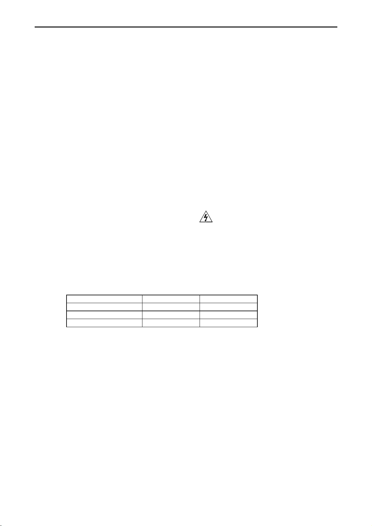
3. ADJUSTMENT of Power Supply
Input voltage AC 100 ~ 240Vac
Rated input voltage AC 90 ~ 264Vac
Frequency 50 / 60 Hz
Rated frequency 47 ~ 63 Hz
DC output
Out voltage +12V +5V
Maximum output current +1.5A +1.5A
Minimum output current 0A +0.1A
Range of voltage Regulation
+15%~-5%
±5%
6
Page 8

4. ADJUSTMENT OF BOARDS
Equipment is connected with boards to be inspected before adjustments. Refer to diagram
below.
A. Connection Method
A-1 VL547 For AU Panel and W/O Audio.
1. R.G.B Signal Cable
2. DC Power Cable
3. LCD Lamp Cables
4. Control Cable
7
Page 9
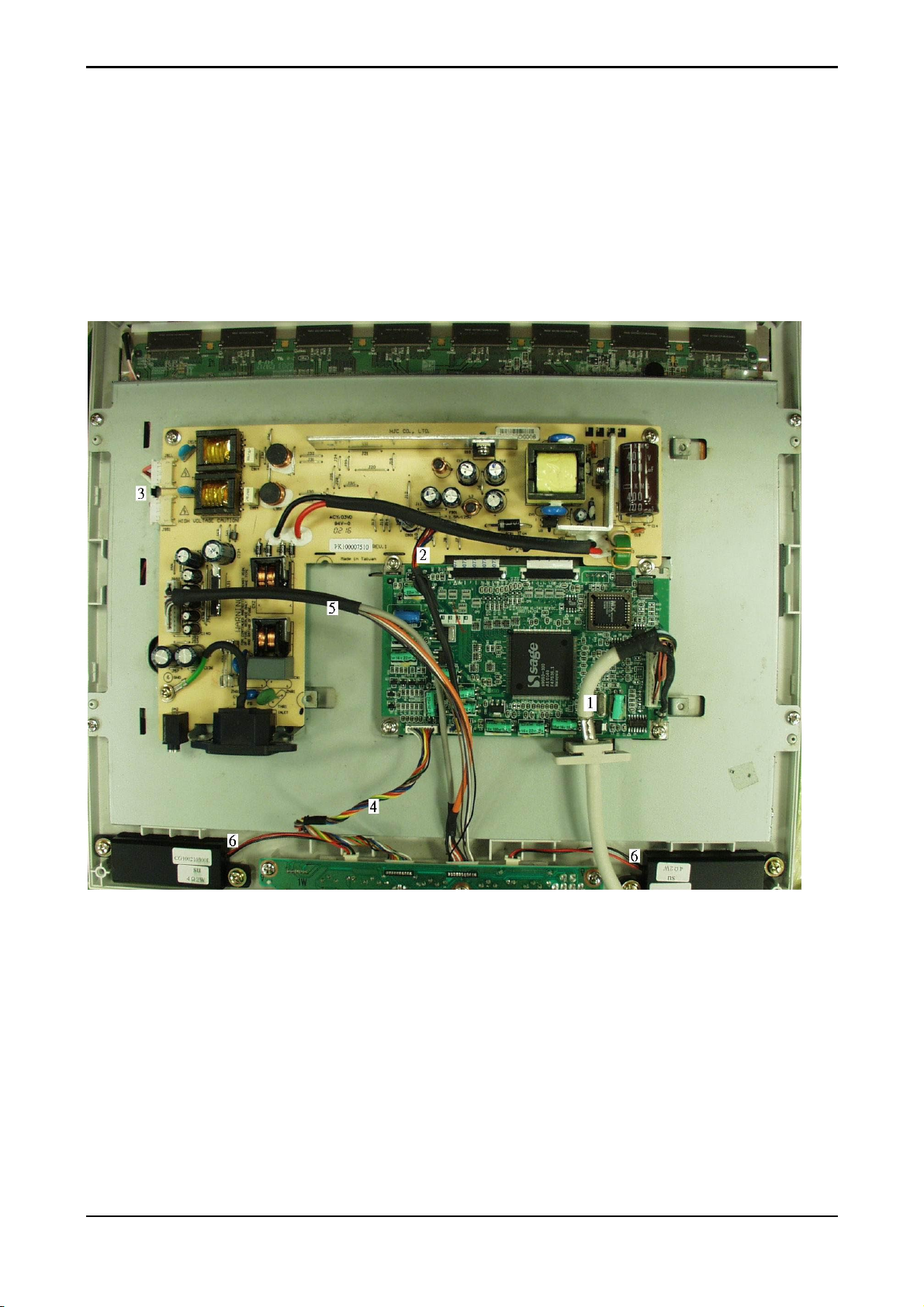
A-2 VL542 For Hannstar Panel W/I Audio
1. R.G.B Signal Cable
2. DC Power Cable
3. LCD Lamp Cables
4. Control Cable
5. Audio Cable
6. Speaker and Wire / Connector
8
Page 10

5. DISPLAY CONTROL BOARD
A. Description
The VL-547 and VL-542 display control board is design to directly convert the R.G.B signals
from VGA Card D-sub port to optimum LCD timing signals so as to construct a high display
quality LCD monitor.
B. Features
•
On board sage chip to detect display timings and control user functions.
• Using sage chip to convert R.G.B signals to digital timing
• Using sage chip to offer full screen expansion function on non-XGA mode(Auto-Zoom).
• Support VESA DPMS function.
• Support DDC2B functions.
9
Page 11
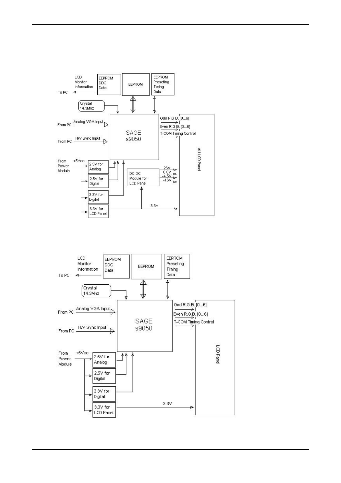
C. Block Diagram (Control CKT)
System Level Interface with Integrated Timing Controller
( VL-547 Diagram Hannstar Panel solution )
( VL-542 Diagram – AU Panel solution)
10
Page 12
C-1 Sage Operation
The s9050-100 is highly-integrated display processors. It has an ADC/PLL block and a
microprocessor integrated on a single chip. The cost-effective s9050-100 is suitable for the
XGA and the s9050 for the SXGA market segment with smaller memory requirements. Other
features include a brand new high-end scaler, Active Color Management, a flexible OSD,
Autoadjust, SureSync
TM
and independent monitoring of the analog interface. A new standalone
on-chip pattern generator has been incorporated to simplify the manufacture of monitors.
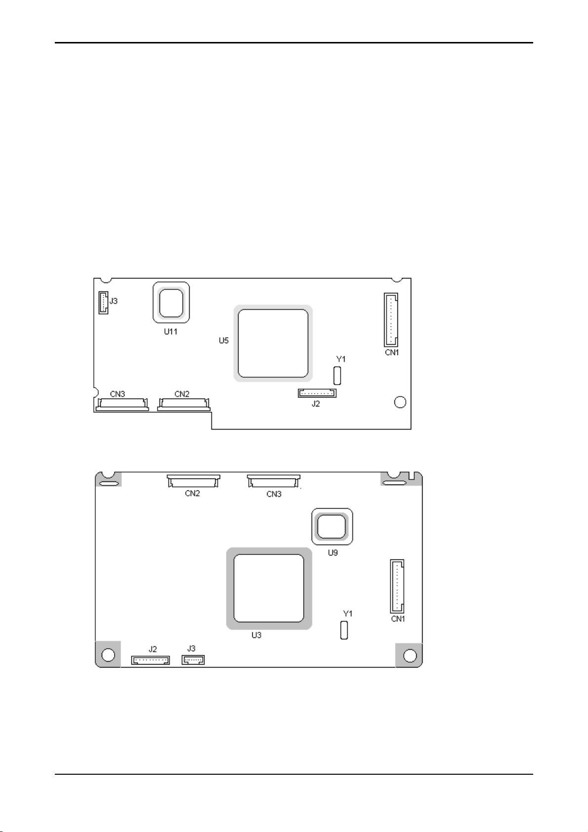
D. Connector Locations
( VL-547 Control Board for AU Panel solution )
( VL-542 Control Board for Hannstar Panel solution )
11
Page 13

E. Connector Type
Location Type Maker Number of pins
CN1 DZ11A91-L8 P1.524 FEMALE 15
J2 96113-1003 E&T 10
J3 96113-0703 E&T 7
CN3 98210-4011 E&T 40
CN2 98210-4011 E&T 40
F. Connector pin assignment
F-1 CN1
Pin NO. Signal
1 Vertical Sync
2 Horizontal Sync
3 Blue Video Ground
4 Blue Video
5 Green Video Ground
6 Green Video
7 Red Video Ground
8 Red Video
9 Shield Ground
10 DDC-SCL
11 DDC-SDA
12 PC-DETECT
13 PC-5V
12
Page 14

F-2
( VL-547 Control Board for AU Panel )
13
Page 15

( VL-542 Control Board for Hannstar Panel )
14
Page 16

F-3 J2
Pin NO. Signal Comment
1 NONE
2 LED-Y Power saving mode
3 LED-G Monitor is ON
4 GND GND
5 KEY-UP Function select counter-clockwise key
6 KEY-Down Function select counter-clockwise key
7 KEY-R Adjust up key
8 KEY-L Adjust down key
9 KEY-POWER Power ON/OFF key
10 GND GND
F-4 J3
Pin NO. Signal Comment
1 +5V VL547 / VL-542 power input
2 +5V VL547 / VL-542 power input
3 GND Ground
4 GND Ground
5 BLON Back Light ON/OFF.
6 MUTE Audio amplifier control signal (Audio unction only )
7 BRIGHT Brightness Adjustment.
15
Page 17

6. VK-546 Control Panel Board
A. Description
The VK-546 is designed to offer an user interfaced control panel which passes and
receives signals to and from power board .
B. Connector and Switch Locations
C. Connector type
Location Type Maker Number of pins
J1 96113-1113 E&T 11 (Audio Function Only)
J2 SCJ-0348-C SC 9 (Audio Function Only)
J3 87502-0200 ACES 2 (Audio Function Only)
J4 87502-0200 ACES 2 (Audio Function Only)
J5 96113-1013 E&T 10
VR1 F1001G-3 B50K FAVOR U 5 (Audio Function Only)
16
Page 18

D. Connector pin Assignment
D-1 J1 (Audio Function Only)
Pin NO. Signal Comment
1 MUTE1 Audio Mute
2 GND GND
3 RIN1 Audio volume adjust line IN R
4 LIN1 Audio volume adjust line IN L
5 RIN2 Audio volume adjust line OUT R
6 LIN2 Audio volume adjust line OUT L
7 GND GND
8 R-EAR EAR Phone out R
9 L-EAR EAR Phone out L
10 ROUT Speaker out R
11 LOUT Speaker out L
D-2 J2 (Audio Function Only)
Pin NO. Signal
1 GND
2 RADOIN 2
3 LADOIN 2
4 RADOIN 1
5 RAUDIO
6 NC
7 LADOIN 1
8 LAUDIO
D-3 J3 & J4 (Audio Function Only)
Pin NO. Signal Comment
1 OUTL(OUTR) Speaker out
2 GND GND
D-4 J5
Pin NO. Signal Comment
1 NONE
2 LED-Y Power saving mode.
3 LED-G Monitor on mode.
4,10 GND Ground
17
Page 19

5 KEY-UP Function select up
6 KEY-DOWN Function select down
7 KEY-R Function select right
8 KEY-L Function select left
9 KEY-PWR Power ON/OFF signal
D-5 VR1 (Audio Function Only)
Volume control , clockwise for increasing ; counter-clockwise for decreasing
D-6 Switch definition
Location Definition
S1 Function select by clockwise direction
S2 Adjust down
S3 Adjust up
S4 Function select by counter-clockwise direction
S5 Power ON/OFF
D-7 LED definition
Location Definition
D1 Green for ON mode; Yellow for DC power off; stand by;
suspend and off mode.
18
Page 20

7. POWER BOARD
A. Description
There are three kind of circuits in this power board-AC/AC, inverter and audio
B. Electrical characteristics
B-1 FOR HANNSTAR PANEL
MIN. TYP. MAX. COMMENT
INPUT VOLTAGE 11.4V 12V 13.8V
INPUT CURRENT -------- 1A 1.2A
BACKLIGHT VOLTAGE 684Vrms 760V rms. --------
LAMP CURRENT 3mA rms. 6mA rms. 7mArms
DRIVING FREQUENCY 40KHz 55KHz 80KHz
EFFICIENCY -------- 75% -------- Vin = 12V
Vin=12V MAX.
BRIGHTNESS
Operating Life Time 40,000 ------- -------- Hours (note)
Note:
Life time(Hr) can be defined as the time in which it continues to operate under the
condition:
Ta=25±3°C, IL=6.0mA
B-2 For AU panel
MIN. TYP. MAX. COMMENT
INPUT VOLTAGE 11.4V 12V 13.8V
INPUT CURRENT -------- 1A 1.2A
BACKLIGHT VOLTAGE 630V rms. 690Vrms
LAMP CURRENT 3mA rms. 6.5mA rms. 8mArms
DRIVING FREQUENCY 40KHz 55KHz 60KHz
EFFICIENCY -------- 75% -------- Vin = 12V
Operating Life Time 30,000 ------- -------- Hours (note)
Vin=12V MAX.
BRIGHTNESS
Note:
Life time(Hr) can be defined as the time in which it continues to operate under the
condition:
Ta=25±3°C, IL=8.0mA
19
Page 21

C. Connector locations
PK100007500
PK100007510
1
CON3
JA2
1
CON1
1
CON2
1
J802
INLET
C-1 Connector type
Location Type Maker Number of pins
CON1 SM02(8.0)B-BHS-1 JST 2
CON2 SM02(8.0)B-BHS-1 JST 2
J802 NC.
CON3 96113-00703 E&T 7
C-2 Connector pin assisnment
C.2.1 CON1 & CON2
Pin NO Signal Comment
1 HV Hish Voltape
2 LV Common
C.2.2 CON3
Pin NO Signal Comment
1,2 Vcc +5V
3,4 GND Ground
5 Ven Back-Light ON/OFF control. Low active
(ON: 0~1V, OFF:3~6U)
6 Mute Audio control signal
7 Vhri Brightness control (min~max)
*For Hannstar pannel: 0.45~2.7V
*For AU Pannel: 0.45~3.3V
20
Page 22

8. CIRCUIT DESCRPTION
A. Micro-Controller Circuit
The U5 (for VL-547 ) or U3 ( for VL-542 ) (s9050-100) is a system controller.
The Y1 is 14.318MHz XTAL.
B. Circuit of Plug and Play
Plug and play allows the serial communication of host PC and peripherals offering minimal
configurations to end users. This monitor supports DDC2B communication protocal.
SDATA and VCLK are input to U4 (for VL-547 ) or U2 ( for VL-542 ) (24LC21A).
C. System Clock
The Y1 (14.318MHz XTAL) supports U5 (for VL-547 ) or U3 ( for VL-542 ) (Sage) reference
clock.
D. Image Engine (Zoom)
The U5 (for VL-547 ) or U3 ( for VL-542 ) (Sage) is a image engine that have following
functions.
(1) The Sage is a IFM ( Input Format Measurement )
(2) The Sage are both high guilty scalar and timing controller chip.
E. Power Regulator
(1) The U12 (for VL-547 ) or U10 ( for VL-542 ) (APL117) is 1A linear regulator that transfer
input voltage from 5V to 3.3V supports U5.
(2) The U13 (for VL-547 ) or U11 ( for VL-542 ) (AIC1084) is 5A linear regulator that transfer
voltage from 5V to 3.3V supports U17 and Panel Vcc.
(3) The U14 (for VL-547 ) or U12 ( for VL-542 ) (APL1117) is 1A linear regulator that transfer
voltage from 5V to 2.5V.
(4) The U15 (for VL-547 ) or U13 ( for VL-542 ) (APL1117) is 1A linear regulator that transfer
voltage from 5V to 2.5V.
21
Page 23

9. INTRODUCTION
A. Front Panel Control and Led
JS558(Without Audio)
Front Panel Controls
Item Control Function
1 DC Power Switch
2 DC Power-On Indicator
3 Function Select Buttons
Adjustment Control
4
Buttons
Press the power switch to switch the monitor
ON/OFF.
LED lights Green color --- Power is ON.
LED lights Yellow --- Monitor is in "Power
Saving Mode".
LED is off --- Power is OFF.
Press either left or right control button for OSD
(On Screen Display) menu selection.
Press the left button to decrease the OSD setting
and press the right button to increase the OSD
setting.
22
Page 24

JS555(With Audio)
Front Panel Controls
Item Control Function
1
Stereo Speakers
2
Speaker Volume Control
3
DC Power Switch
4
DC Power-On Indicator
5
Function Select Buttons
Adjustment Control
6
Buttons
7
External Headphone Jack
PC Audio Stereo output.
Increase Volume - Turn knob clockwise.
Decrease Volume - Turn knob counter clockwise
Press the power switch to switch the monitor
ON/OFF.
LED lights Green color --- Power is ON.
LED lights Yellow --- Monitor is in "Power Saving
Mode".
LED is off --- Power is OFF.
Press either left or right control button for OSD (On
Screen Display) menu selection.
Press the left button to decrease the OSD setting
and press the right button to increase the OSD
setting.
The monitor speakers will be disabled when using
an external headphone or external speakers.
23
Page 25

B. Rear Panel connector Input Signals
Rear Panel Cable and Connector
Item Cable / Connector Function
1 Signal Cable Connect the video port
2 AC IN Power Connect Connect the AC power cord
3
Audio connector
(JS555 Only)
Connect the audio port
24
Page 26

10. TROUBLESHOOTING
A. Main Procedure
25
Page 27

A-1 Power Circuit Troubleshooting
26
Page 28

A-2 Backlights Troubleshooting
27
Page 29

A-3 Performance Troubleshooting
28
Page 30

A-4 Function Troubleshooting
29
Page 31

Audio Board
Connector
J1
11
10
9
8
7
6
5
4
3
2
1
E&T_96113_1113
LOUT
ROUT
L_EAR
R_EAR
LIN_2
RIN_2
LIN_1
LIN_1
MUTE
J2
4
LI1 LO
2
LI2
7
RI1
3
RI2
SCJ-0348-C
3'
2
3
NC
RO
GND
5
6
8
1
J3
12ACES_87502_0200
STRAIGHT/2.5
J4
12ACES_87502_0200
STRAIGHT/2.5
VR1
50K
2'
1,1'
VR1
Main Board
Connector
J5
MUTE
1
LED_Y
2
LED_G
3
GND
4
KEY_UP
5
KEY_DOWN
6
KEY_R
7
KEY_L
8
KEY_PWR
9
10
E&T_96113_1013
GND
S1
PT-002-82
S2
PT-002-82S3PT-002-82S4PT-002-82S5PT-002-82
3
3' 2'
2
1
1'
3
1
2
D1
LYG2093 YEL/GRN
No. 0417
VK-546 KEY BOARD (CONTROL PANEL)
30
Page 32

CN1
1
2
3
4
5
6
7
8
9
10
11
12
13
E&T-4500-13
VSYNC_IN
HSYNC_IN
BGNDA
PC_B
GGNDA
PC_G
RGNDA
PC_R
GND_POWER
SCL_for_DDC
SDA_for_DDC
CABLE_Dect
5V_DDC
PC_R
RGNDA
PC_G
GGNDA
PC_B
R2
75
1%
R4
75
1%
R6
75
1%
L2
L4
L1
R1
100
1%
R3
100
1%
R5
100
1%
C1
2.2p#
C2
2.2p#
C3
2.2p#
RIN_P
RIN_N
GIN_P
GIN_N
BIN_P
A3.3V
L3
3.3VCC
5VCC
CABLE
DDC_DSA
DDC_SCL
HSYNC
VSYNC
ESD PROTECTION
C4
0.1u#
1
2
3
DALC208SC6#
D3
5V6#D45V6#
6
5
4
ZD1
PC_GPC_R
PC_B
D5
5V6#D65V6#
VSYNC
DDC_SCL
DDC_SDA
BGNDA
R13
R14
R15
22
100
100
R9
27K
EDID
5V_DDC
R10
27K
U2
8
VCC
7
VCLK
6
SCL
5
SDA
24LC21A
NC
NC
NC
GND
BIN_N
A3.3V
D2D1
5VCC
R7
R12
1K
100
R8
100
C6
10p
C7
10p
HSYNC
1
2
3
4
C8
0.1u
VSYNC
R11
1K
U1
1
A1
VCC
3
A2
Y1
A3
A4
A5
A6
GND
Y1
Y2
Y2
Y3
Y3
Y4
Y4
Y5
Y5
Y6
Y6
5
9
11
13
7
SN74LVC14PWR
14
2
4
6
8
10
12
C5
0.1u
AHSYNC
AVSSYNC
No. 0417
VL-542 MAIN BOARD (DISPLAY CONTROL) - SHEET 1
31
Page 33

VDD_D_CORE1
VDD_D_CORE2
VDD_D_CORE3
VDD_D_CORE4
VDD_D_CORE5
VDD_D_CORE6
VDD_D_CORE7
VDD_D_CORE8
VDD_D_CORE9
DVDD
VDD_D_PNLPLL
VDD_D_MCPLL
3.3VCC
TM_AVDD
TM_VDD0
TM_VDD1
TM_VDD2
TM_VDDC
2.5VDD
TM_VDD25_PLL
TM_DVDD1
TM_DVDD2
RST#
KEY-R
KEY-DOWN
KEY-UP
KEY-L
DDC_SCL
DDC_SDA
AHSYNC
2.5VCC
L5
C24
C27
VSS_D_CORE1
VSS_D_CORE2
VSS_D_CORE3
VSS_D_CORE4
VSS_D_CORE5
VSS_D_CORE6
VSS_D_CORE7
VSS_D_CORE8
VSS_D_CORE9
DVSS
VSS_D_PNLPLL
VSS_D_MCPLL
TM_AVSS
TM_VSS0
TM_VSS1
TM_VSS2
TM_VSSC
TM_VSS25_PLL
TM_DVSS1
TM_DVSS2
A2.5V
L7
VDD_A
VDD_A
VDD_A
VDD_A
3.3VCC
L8
VDD_D_IO1
VDD_D_IO2
VDD_D_IO3
VDD_D_IO4
VDD_D_IO5
VDD_D_IO6
VDD_D_IO7
PNL_CLKO
L6
C19 1000p
C21 0.1u
C28 0.1u
C30 0.1u
C31 0.1u
C32 0.1u
C37
22u/50V
C43 0.1u
C44 0.1u
C45 0.1u
C46 0.1u
C47 0.1u
C49 0.1u
C51 0.1u
C53
10u/10V
C56
470p
VSS_A
VSS_A
VSS_A
VSS_A
R29
22
R30
3.3K
C23 0.1u
C25 1000p
VSS_D_IO1
VSS_D_IO2
VSS_D_IO3
VSS_D_IO4
VSS_D_IO5
VSS_D_IO6
VSS_D_IO7
C57
0.01u#
C10
22p
R23 47
R24 0
C54
10u/10v
U4
1
2
3
4
FS781
C16
22p
XIN
XOUT
S1
LF
R19
1M
C26 10u/10V
C29 0.1u
R25 10
C35 10u/10V
C38 0.1u
R26 10
VDD_D_IO1
C55
0.1u
8
VDD
7
S0
6
FSOUT
5
VSS
C9 0.1u
C11 0.1u
C12 0.1u
C13 0.1u
C14 0.1u
C15 0.1u
C17 0.1u
C18 0.1u
C20 0.1u
C22 0.1u
0.1u
22u/50V
C36 0.1u
C39 0.1u
C40 0.1u
C41 0.1u
C42 0.1u
C48 0.1u
C50 0.1u
C52 0.1u
AVSYNC
Y1
14.318MHz
RIN_N
RIN_P
GIN_N
GIN_P
BIN_N
BIN_P
PWM0
SCL
SDA
LEDY
TXD
RXD
MCA[16..17]
MCA[8..15]
R28
10K
R31
1K#
3.3VCC
R20 1K#
R21 1K
R22 1K
R22 1K
VDD_A_PLL
VSS_A_PLL
VDD_A_PLL
VSS_A_PLL
VSS_A_PLL
VDD_D_PLL
VDD_D_PLL
DVDD
DVSS
VSS_A
VDD_A
VDD_A
VSS_A
VSS_A
VDD_A
VDD_A
VDD_A
VSS_A
VSS_A
VDD_A
VDD_A
VSS_A
VSS_A
VSS_A
VDD_A
VDD_D_CORE1
VSS_D_CORE1
VDD_D_CORE2
VSS_D_CORE2
R27 10K
PNL_CLKI
MCA17
MCA16
MCA15
MCA14
MCA13
MCA12
MCA11
MCA10
MCA9
MCA8
R16 22#
R17 22#
R18 10K
1
MCOP1
2
MCOP2
3
XTALIN
4
XTALOUT
5
VDD_A_PLL
6
VSS_A_PLL
7
VDD_A_PLL
8
VSS_A_PLL
9
VSS_A_PLL
10
VDD_D_PLL
11
VDD_D_PLL
12
DVDD
13
DVSS
14
VSS_A
15
VDD_A
16
RIN_N
17
RIN_P
18
VDD_A
19
VSS_A
20
VSS_A
21
VDD_A
22
VDD_A
23
GIN_N
24
GIN_P
25
VDD_A
26
VSS_A
27
VSS_A
28
VDD_A
29
BIN_N
30
BIN_P
31
VDD_A
32
VSS_A
33
VSS_A
34
VSS_A
35
VDD_A
36
VDD_D_CORE1
37
VSS_D_CORE1
38
GPIO0
39
GPIO1
40
GPIO2
41
GPIO3
42
VDD_D_CORE2
43
VSS_D_CORE2
44
MCTX
45
MCRX
46
INTR
47
MCA19
48
MCA18
49
MCA17
50
MCA16
51
MCA15
52
MCA14
MCALE
MCRD#
MCWR#
MCCS#
MCAD[0..7]
VSS_D_IO7
VDD_D_IO7
VDD_D_CORE9
VSS_D_CORE9
TM_AVDD
TM_AVSS
TM_DVSS2
TM_VDD25_PLL
TM_VSS25_PLL
TM_VDDC
TM_VSSC
TM_VDD0
TM_VSS0
TM_VDD1
TM_VSS1
TM_VDD2
TM_DVDD2
208
207
206
205
204
203
202
201
200
199
198
197
196
195
194
193
192
191
190
189
188
187
186
185
184
183
182
181
180
179
178
VS
HS
SCL
SDA
TEST
GPIO20
RST#
GPIO21
GPIO23
GPIO22
VSS_D_IO7
VDD_D_IO7
TM_AVSS
TM_AVDD
TM_EXTRES
VSS_D_CORE9
VDD_D_CORE9
TM_VDDC
TM_DVSS2
TM_DVDD2
TM_VSS25_PLL
TM_VDD25_PLL
TM_RX0P
TM_VSS0
TM_RX0N
TM_RXCP
TM_RXCN
TM_VSSC
TM_RX1N
TM_VDD1
TM_VDD0
TM_VSS2
177
176
175
174
173
172
TM_VSS1
TM_RX1P
TM_RX2P
TM_RX2N
TM_VDD2
U3
S9050
MCALE
MCRD#
MCWR#
MCCS#
MCCS1#
VDD_D_CORE3
VSS_D_CORE3
VDD_D_IO1
VSS_D_IO1
MCA8
MCAD7
MCAD6
MCAD5
MCAD4
MCAD3
MCAD2
MCAD1
MCAD0
VDD_D_CORE4
VSS_D_CORE4
GPIO10
GPIO18
GPIO17
GPIO16
GPIO15
GPIO14
GPIO13
GPIO12
VDD_D_IO2
VSS_D_IO2
MCA13
MCA12
MCA11
MCA10
MCA9
5354555657
585960616263646566676869707172737475767778798081828384858687888990919293949596979899100
VDD_D_CORE3
VSS_D_CORE3
VDD_D_IO1
MCAD7
MCAD6
MCAD5
MCAD4
MCAD3
MCAD2
MCAD1
MCAD0
LEDG
KEY=POWER
VSS_D_IO1
VDD_D_CORE4
VSS_D_CORE4
VDD_D_CORE5
VDD_D_IO2
VSS_D_IO2
VDD_D_CORE5
VSS_D_CORE5
TM_DVSS1
TM_DVDD1
VDD_D_CORE8
VSS_D_CORE8
VDD_D_IO6
VDD_A_PNLPLL
VSS_A_PNLPLL
VSS_A_PNLPLL
VDD_A_PNLPLL
VDD_A_MCPLL
VSS_A_MCPLL
VSS_A_MCPLL
VDD_A_MCPLL
VSS_D_IO5
VDD_D_IO5
171
170
169
168
167
166
165
164
163
162
161
160
159
158
157
TM_VSS2
TM_DVSS1
TM_DVDD1
VDD_D_IO6
VSS_D_CORE8
VSS_A_PNLPLL
VSS_A_PNLPLL
VDD_D_CORE8
VSS_D_CORE5
GPIO11
GPIO10
GPIO9
VDD_A_PNLPLL
VDD_A_PNLPLL
GPIO8
GPIO7
GPIO6
GPIO5
GPIO4
PNL_CLKO
VSS_A_MCPLL
VSS_A_MCPLL
VDD_A_MCPLL
PD01
PNL_CLKI
PD00
101
VSS_D_IO5
VDD_D_IO5
VDD_A_MCPLL
VSS_D_IO4
VDD_D_IO4
VSS_D_CORE7
VDD_D_CORE7
PSCLK
VSS_D_IO3
VDD_D_IO3
VSS_D_CORE6
VDD_D_CORE6
PD02
PD03
PD04
102
103
104
PD47
PD46
PD45
PD44
PD43
PD42
PD41
PD40
PD39
PD38
PD37
PD36
PD35
PD34
PD33
PD32
PD31
PD30
PD29
PD28
PD27
PD26
PD25
PD24
PD23
PD22
PD21
PD20
PD19
PD18
PD17
PD16
PD15
PD14
PD13
PD12
PD11
PD10
PD09
PD08
PD07
PD06
PD05
PNL_CLKO
PNL_CLKI
MUTE
PENVDD
PENBLK
ISTH
ILOAD
IPOL
IREV
ISTV1
ISTV2
ICPV
IOE
156
155
154
151
153
151
150
149
148
147
146
145
VSS_D_IO4
144
VDD_D_IO4
143
VSS_D_CORE7
142
VDD_D_CORE7
141
140
139
138
137
136
135
134
133
132
131
130
129
128
127
126
125
124
123
VSS_D_IO3
122
VDD_D_IO3
121
VSS_D_CORE6
120
VDD_D_CORE6
119
118
117
116
115
114
113
112
111
110
109
108
107
106
105
PD[0..35]
PD00
PD01
PD02
PD03
PD04
PD35
PD34
PD33
PD32
PD31
PD30
PD29
PD28
PD27
PD26
PD25
PD24
PD23
PD22
PD21
PD20
PD19
PD18
PD17
PD16
PD15
PD14
PD13
PD12
PD11
PD10
PD09
PD08
PD07
PD06
PD05
ICPH
No. 0417
VL-542 MAIN BOARD (DISPLAY CONTROL) - SHEET 2
32
Page 34

DEBUG PORT
5VCC
C67
0.1u
LEDY
C50
0.1u#
LMB10M3X-4.38
VCC
3
DIO/MA730
1
2
GND
RESET
LM810M3X-4.38
R48
4K7
R54 100
HEADER 4#
U7
VCC
Reset
GND
U5
3
D0
4
D1
7
D2
8
D3
13
D4
14
D5
17
D6
18
D7
11
75HCT373
U6
3
D0
4
D1
7
D2
8
D3
13
D4
14
D5
17
D6
18
D7
11
75HCT373
U9
13
D0
14
D1
15
D2
17
D3
18
D4
19
D5
20
D6
21
D7
5VCC
20
10
5VCC
20
10
5VCC
16
C58 0.1u
2
Q0
5
Q1
6
Q2
9
Q3
12
Q4
15
Q5
16
Q6
19
Q7
1
OCG
2
Q0
5
Q1
6
Q2
9
Q3
12
Q4
15
Q5
16
Q6
19
Q7
1
OCG
32
A0
A1
A2
A3
A4
A5
A6
A7
A8
A9
A10
A11
A12
A13
A14
A15
A16
A17
CE
OE
PGM
VPP
R55 0#
C60 0.1u
MCA0
MCA1
MCA2
MCA3
MCA4
MCA5
MCA6
MCA7
C68 0.1u
12
MCA0
11
MCA1
10
MCA2
9
MCA3
8
MCA4
7
MCA5
6
MCA6
5
MCA7
MCA8
27
MCA9
26
MCA10
23
MCA11
25
4
MCA12
28
MCA13
29
MCA14
3
MCA15
MCA16
2
JMCA17
30
CS0#
22
MCRD#
24
JMCWR#
31
1
MCA16
MCA17
KEY-POWER
R43
10K
KEY-UP
KEY-DOWN
KEY-R
KEY-L
MCA[0..7]
MCA[8..15]
R44
R45
10K
10K
R46
10K
R47
10K
5VCC
5VCC
R35
R34
10K
10K
C62
C61
0.1u
0.1u
R51 0
R53 0#
R36
10K
C63
0.1u
R37
10K
C64
0.Iu
R38
10K
C65
0.1u
CS0#
MCRD#
MCWR#
MCA16
MCA17
LED-Y
LED-G
E&T_96113-1003
J2
1
2
3
4
5
6
7
8
9
10
5VCC
5VCC
MCAD[16..17]
U8
8
5
6
4
R42
180
Q3
2SA1036K
C66
0.1u
VCC
SDA
SCL
GND
AT24LC16
MCA[0..7]
TEST
A2
A1
A0
7
7
3
3
2
2
1
1
LED-G
MCALE
MCAD16
MCAD17
MCAD0
MCAD1
MCAD2
MCAD3
MCAD4
MCAD5
MCAD6
MCAD7
MCALE
MCAD0
MCAD1
MCAD2
MCAD3
MCAD4
MCAD5
MCAD6
MCAD7
MX26C1000BQC
5VCC
22K
LED-Y
R33
10K#
Q1
DTC124EK
DRAIN
2N7002
SOT-23B
1
GATE
3
SOURCE
LEDG
RST#
2
RXD
TXD
SDA
SCL
R50
4K7
5VCC
R40
10K
R52 100
R41
10K
5VCC
RST
R49
180
Q2
2N7002
R32
10K#
R39 10K
22K
J1
1
2
3
4
3
2
1
E&T_96113-0703
No. 0417
R56 1K
BLON low enable (3.3V or 5V)
L9
STC2228
C70
J3
1
2
3
4
5
6
7
BLON
BRIGHT
CABLE
0.1u
R59 0#
R63 10K
R64 100
C71
0.1u
5VCC
MUTE
C72
0.1u
C69
0.1u
Q4
2SC2411K
R60 20K R61 10K
Q5
+
C73
22u/50V
22K
22K
DTC124EK
R57
4K7
R58 1K
R63 10K
PWM0
PENBKL
COLLECTOR
3
DTC124EK
SOT-23B
2
BASE
1
EMITTER
COLLECTOR
2SC2411K
SOT-23B
2
BASE
3
EMITTER
1
COLLECTOR
2SA1036K
SOT-23B
2
BASE
3
EMITTER
1
VL-542 MAIN BOARD (DISPLAY CONTROL) - SHEET 3
33
Page 35

5VCC
U10
APL1117-3.3
3
2
VOVI
3.3VCC
C76
0.1u
C81
0.1u
C84
22u/50V
+
C74
22u/50V
+
C79
100u/16V
+
C86
0.1u
GND
1
U11
AIC1084CE-3.3
3
GND
1
U12
APL1117-2.5
3
GND
VOVI
VOVI
1
2
2
C85
100u/16V
+
C75
100u/16V
+
C80
220u/16V
+
C87
0.1u
C77
0.1u
C82
0.1u
2.5VCC
C78
0.1u
C83
0.1u
3.3VLCD
2 Vout
APL1117-3.3
SOT-223
1
2
Vout
GND
2 Vout
AIC1084CE-3.3
TO-252
1
2
GND
Vout
2 Vout
APL1117-2.5
SOT-223
3
Vin
3
Vin
No. 0417
2
Vout
3
Vin
C88
22u/50V
C90
0.1u
U13
APL1117-2.5
3
GND
VOVI
1
100u/16V
1
GND
2
++
C89
A2.6V
C91
0.1u
VL-542 MAIN BOARD (DISPLAY CONTROL) - SHEET 4
34
Page 36

PD[0..35]
PD35
PD34
PD33
PD32
PD31
PD30
PD29
PD28
PD27
PD26
PD25
PD24
PD23
PD22
PD21
PD20
PD19
PD18
PD17
PD16
PD15
PD14
PD13
PD12
PD11
PD10
PD9
PD8
PD7
PD6
PD5
PD4
PD3
PD2
PD1
PD0
1
2
3
4
1
2
3
4
1
2
3
4
1
2
3
4
1
2
3
4
1
2
3
4
1
2
3
4
1
2
3
4
1
2
3
4
ISTH
ILOAD
IPOL
IREV
ISTV1
ISTV2
ICPV
IOE
RP1 22
RP2 22
RP3 22
RP4 22
RP5 22
RP6 22
RP7 22
RP8 22
RP9 22
1
VDD+9V
2
VDD+9V
3
GND
4
GND
5
EB5
6
EB4
7
EB3
8
EB2
9
EB1
10
EB0
11
GND
12
EG5
13
EG4
14
EG3
15
EG2
16
EG1
17
EG0
18
GND
19
ER5
20
ER4
21
ER3
22
ER2
23
ER1
24
ER0
25
GND
26
CPH1
27
GND
28
GND
29
STH
30
LOAD
31
POL
32
REV
33
GND
34
GND
35
STV1
36
STV2
37
CPV
38
OE
39
GND
40
GND
E&T_98210-4011-0.50m
1
VDD
2
VDD
3
GND
4
GND
5
OB5
6
OB4
7
OB3
8
OB2
9
OB1
10
OB0
11
GND
12
OG5
13
OG4
14
OG3
15
OG2
16
OG1
17
OG0
18
GND
19
OR5
20
OR4
21
OR3
22
OR2
23
OR1
24
OR0
25
GND
26
CPH2
27
GND
28
GND
29
NC
30
NC
31
VGH
32
NC
33
VGL
34
NC
35
VGC
36
NC
37
NC
38
NC
39
GND
40
GND
E&T_98210-4011-0.50m
R67
1K
CPH1
LOAD
STV1
STV2
CPH2
BE5
BE4
BE3
BE2
BE1
BE0
GE5
GE4
GE3
GE2
GE2
GE0
RE5
RE4
RE3
RE2
RE1
RE0
STH
POL
REV
CPV
OE
BO5
BO4
BO3
BO2
BO1
BO0
GO5
GO4
GO3
GO2
GO2
GO0
RO5
RO4
RO3
RO2
RO1
RO0
L13
C94
0.1u
10p
10p
10p
10p
10p
10p
10p
10p
C98
C99
C100
C101
C102
C103
C104
C105
CP1 47p
4
3
2
1
CP2 47p
4
3
2
1
CP3 47p
4
3
2
1
CP4 47p
4
3
2
1
CP5 47p
4
3
2
1
CP6 47p
4
3
2
1
CP7 47p
4
3
2
1
CP8 47p
4
3
2
1
CP9 47p
4
3
2
1
5
6
7
8
5
6
7
8
5
6
7
8
5
6
7
8
5
6
7
8
5
6
7
8
5
6
7
8
5
6
7
8
5
6
7
8
LOAD
POL
REV
STV1
STV2
CPV
OE
STH
ICPH
3.3VLCD
L12
PENVDD
R65
R66
R68
1M
22K
22K
L13
22
L13
22
S
G
C96
1000p
R69
100K
Q6
DTC124EK
C92
10p
C93
10p
U14
D
S12305DS
CPH1
CPH2
LCD3.3VCC
+
+
C95
220u/50V
COLLECTOR
3
DTC124EK
SOT-23B
2
BASE
3 D
SI2305DS
SOT-23
1 G
1
EMITTER
2 S
C97
0.1u
0
0
8
7
6
5
8
7
6
5
8
7
6
5
8
7
6
5
8
7
6
5
8
7
6
5
8
7
6
5
8
7
6
5
8
7
6
5
R70
22
R71
22
R72
22
R73
22
R74
22
R75
22
R76
22
R77
22
BE5
BE4
BE3
BE2
BE1
GE0
GE5
GE4
GE3
GE2
GE1
GE0
RE5
RE4
RE3
RE2
RE1
RE0
BO5
BO4
BO3
BO2
BO1
BO0
GO5
GO4
GO3
GO2
GO1
GO0
RO5
RO4
RO3
RO2
RO1
RO0
L14
L15
L16
L17
L18
L19
L20
L21
0
0
0
0
0
0
0
0
CN2
CN3
No. 0417
VL-542 MAIN BOARD (DISPLAY CONTROL) - SHEET 5
35
Page 37

KEY BOARD
(VK-546)
POWER/INVERTER
BOARD
MAIN BOARD
(VL-542)
36
Page 38

THE UPDATED PARTS LIST
FOR THIS MODEL IS
AVAILABLE ON ESTA
Page 39

Hitachi, Ltd. Tokyo, Japan
International Sales Division
THE HITACHI ATAGO BUILDING,
No. 15 –12 Nishi Shinbashi, 2 – Chome,
Minato – Ku, Tokyo 105-8430, Japan.
Tel: 03 35022111
HITACHI EUROPE LTD,
Whitebrook Park
Lower Cookham Road
Maidenhead
Berkshire
SL6 8YA
UNITED KINGDOM
Tel: 01628 643000
Fax: 01628 643400
Email: consumer-service@hitachi-eu.com
HITACHI EUROPE GmbH
Munich Office
Dornacher Strasse 3
D-85622 Feldkirchen bei München
GERMANY
Tel: +49-89-991 80-0
Fax: +49-89-991 80-224
Hotline: +49-180-551 25 51 (12ct/min)
Email: HSE-DUS.service@hitachi-eu.com
HITACHI EUROPE srl
Via Tommaso Gulli N.39, 20147
Milano, Italia
ITALY
Tel: +39 02 487861
Tel: +39 02 38073415 Servizio Clienti
Fax: +39 02 48786381/2
Email: customerservice.italy@hitachi-eu.com
HITACHI EUROPE S.A.S
Lyon Office
B.P. 45, 69671 BRON CEDEX
FRANCE
Tel: 04 72 14 29 70
Fax: 04 72 14 29 99
Email: france.consommateur@hitachi-eu.com
HITACH EUROPE AB
Egebækgård
Egebækvej 98
DK-2850 Nærum
DENMARK
Tel: +45 43 43 6050
Fax: +45 43 60 51
Email: csgnor@hitachi-eu.com
Hitachi Europe Ltd
Bergensesteenweg 421
1600 Sint-Pieters-Leeuw
BELGIUM
Tel: +32 2 363 99 01
Fax: +32 2 363 99 00
Email: sofie.van.bom@hitachi-eu.com
www.hitachidigitalmedia.com
HITACHI EUROPE S.A.
364 Kifissias Ave. & 1, Delfon Str.
152 33 Chalandri
Athens
GREECE
Tel: 1-6837200
Fax: 1-6835964
Email: service.hellas@hitachi-eu.com
HITACHI EUROPE S.A.
Gran Via Carlos III, 101-1
08028 Barcelona
SPAIN
Tel: 93 409 2550
Fax: 93 491 3513
Email: atencion.cliente@hitachi-eu.com
HITACHI Europe AB
Box 77 S-164 94 Kista
SWEDEN
Tel: +46 (0) 8 562 711 00
Fax: +46 (0) 8 562 711 13
Email: csgswe@hitachi-eu.com
HITACHI EUROPE LTD (Norway) AB
STRANDVEIEN 18
1366 Lysaker
NORWAY
Tel: 67 5190 30
Fax: 67 5190 32
Email: csgnor@hitachi-eu.com
HITACHI EUROPE AB
Neopoli / Niemenkatu 73
FIN-15140 Lahti
FINLAND
Tel : +358 3 8858 271
Fax: +358 3 8858 272
Email: csgnor@hitachi-eu.com
HITACHI EUROPE LTD
Na Sychrove 975/8
101 27 Pr aha 10 – Bohdalec
CZECH REPUBLIC
Tel: +420 267 212 383
Fax: +420 267 212 385
Email: csgnor@hitachi-eu.com
 Loading...