

Page 1
SERVICEMANUAL
MANUELD'ENTRETIEN
WARTUNGSHANDBUCH
CAUTION:
Beforeservicingthischassis,itisimportantthattheservicetechnicianreadthe“Safety
Precautions”and“ProductSafetyNotices”inthisservicemanual.
No. 0531
CML152XW
DatacontainedwithinthisService
manualissubjecttoalterationfor
improvement.
ATTENTION:
Avantd’effectuerl’entretienduchâassis,letechniciendoitlireles«Précautionsdesécurité»
etles«Noticesdesécuritéduproduit»présentésdansleprésentmanuel.
VORSICHT:
VorÖffnendesGehäuseshatderService-Ingenieurdie„Sicherheitshinweise“und„Hinweise
zurProduktsicherheit“indiesemWartungshandbuchzulesen.
CONTENTS
SAFETY................................................................................................................................................................2
ELECTRICALREQUIREMENTS.........................................................................................................................5
ADJUSTMENTCONDITIONS.............................................................................................................................8
ADJUSTMENTOFBOARDS...............................................................................................................................9
CIRCUITDESCRIPTION...................................................................................................................................20
TROUBLESHOOTING.......................................................................................................................................23
SCHEMATICDIAGRAMS.................................................................................................................................28
EXPLODEDVIEWS..........................................................................................................................................38
REPLACEMENTPARTSLIST.........................................................................................................................40
Lesdonnéesfourniesdansleprésent
manueld’entretienpeuventfairel’objet
demodificationsenvuedeperfectionner
leproduit.
DieindiesemWartungshandbuch
enthaltenenSpezifikationenkönnensich
zwecksVerbesserungenändern.
SPECIFICATIONSANDPARTSARESUBJECTTOCHANGEFORIMPROVEMENT
HIGHRESOLUTIONCOLOURLCDDISPLAYMONITOR
APR2001
Page 2

ENGLISH
SAFETY PRECAUTIONS
WARNING: The following precautions must be observed.
ALL PRODUCTS
Before any service is performed on the chassis an
isolation transformer should be inserted between the
power line and the product.
1. When replacing the chassis in the cabinet, ensure
all the protective devices are put back in place.
2. When service is required, observe the original
lead dressing. Extra precaution should be taken to
ensure correct lead dressing in any high voltage
circuitry area.
3. Many electrical and mechanical parts in
HITACHI products have special safety related
characteristics. These characteristics are often not
evident from visual inspection, nor can the
protection afforded by them necessarily be
obtained by using replacement components rated
for higher voltage, wattage, etc. Replacement
parts which have these special safety
characteristics are identified by marking with a
! on the schematics and the replacement parts
list.
The use of a substitute replacement component
that does not have the same safety characteristics
as the HITACHI recommended replacement one,
shown in the parts list, may create electrical
shock, fire, X-radiation, or other hazards.
4. Always replace original spacers and maintain lead
lengths. Furthermore, where a short circuit has
occurred, replace those components that indicate
evidence of overheating.
5. Insulation resistance should not be less than 2M
ohms at 500V DC between the main poles and
any accessible metal parts.
6. No flashover or breakdown should occur during
the dielectric strength test, applying 3kV AC or
4.25kV DC for two seconds between the main
poles and accessible metal parts.
7. Before returning a serviced product to the
customer, the service technician must thoroughly
test the unit to be certain that it is completely safe
to operate without danger of electrical shock. The
service technician must make sure that no
protective device built into the instrument by the
manufacturer has become defective, or
inadvertently damaged during servicing.
CE MARK
1. HITACHI products may contain the CE mark on
the rating plate indicating that the product
contains parts that have been specifically
approved to provide electromagnetic
compatibility to designated levels.
2. When replacing any part in this product, please
use only the correct part itemised in the parts list
to ensure this standard is maintained, and take
care to replace lead dressing to its original state,
as this can have a bearing on the electromagnetic
radiation/immunity.
PICTURE TUBE
1. The line output stage can develop voltages in
excess of 25kV; if the E.H.T. cap is required to be
removed, discharge the anode to chassis via a
high value resistor, prior to its removal from the
picture tube.
2. High voltage should always be kept at the rated
value of the chassis and no higher. Operating at
higher voltages may cause a failure of the picture
tube or high voltage supply, and also, under
certain circumstances could produce X-radiation
levels moderately in excess of design levels. The
high voltage must not, under any circumstances,
exceed 29kV on the chassis (except for projection
Televisions).
3. The primary source of X-radiation in the product
is the picture tube. The picture tube utilised for
the above mentioned function in this chassis is
specially constructed to limit X-radiation. For
continued X-radiation protection, replace tube
with the same type as the original HITACHI
approved type
4. Keep the picture tube away from the body while
handling. Do not install, remove, or handle the
picture tube in any manner unless shatterproof
goggles are worn. People not so equipped should
be kept away while picture tubes are handled
LASERS
If the product contains a laser avoid direct exposure to
the beam when the cover is open or when interlocks are
defeated or have failed.
2
Page 3

FRANÇAIS
CONSIGNES DE SECURITE
AVERTISSEMENT: vous devez respecter les précautions suivantes
POUR TOUS LES PRODUITS
Avant d’effectuer une intervention d’entretien sur le
châssis, vous devez insérer un transformateur d’isolement
entre la ligne d’alimentation électrique et le produit.
1. Lors de la remontage du châssis dans le coffret,
vérifiez que tous les dispositifs de protection sont
remis en place.
2. Lorsqu’une intervention d’entretien s’avère
nécessaire, respectez l’agencement d’origine des
conducteurs. Vous devez prendre des précautions
supplémentaires pour garantir un agencement correct
des conducteurs dans toutes les zones où des circuits
haute tension sont présents.
3. De nombreux composants électriques et mécaniques
des appareils HITACHI ont des caractéristiques
spéciales de sécurité. Bien souvent, ces
caractéristiques ne sont pas évidentes lors d’un
examen visuel et la protection qu’ils offrent n’est pas
forcément garantie si vous utilisez des composants de
rechange conçus, par exemple, pour une tension plus
élevée, une puissance plus forte. Les pièces de
rechange qui offrent des caractéristiques spéciales de
sécurité sont identifiées par un repérage comportant
le symbole ! sur les schémas et sur la
nomenclature des pièces de rechange.
L’emploi d’un composant de rechange qui ne
respecte pas les mêmes caractéristiques de sécurité
que la pièce de rechange que recommande HITACHI
et qui figure dans la nomenclature risque de
provoquer un choc électrique, un incendie, des rayons
X ou d’autres dangers.
4. Remettez toujours en place les entretoises d’origine
et respectez la longueur des conduites. En outre, à la
suite d’un court-circuit, remplacez les composants
présentant des signes de surchauffe.
5. La résistance d’isolement doit être supérieure ou
égale à 2 méga ohms à 500 V c.c. entre les pôles
principaux et des composants métalliques
accessibles, quels qu’ils soient.
6. Aucun claquage et aucune rupture ne doit se produire
pendant l’essai de résistance diélectrique à la suite de
l’application d’une tension de 3 kV c.a. ou de 4,35
kV c.c. pendant deux secondes entre les pôles
principaux et des composants métalliques
accessibles.
7. Avant de remettre au client un produit qui a fait
l’objet d’un entretien, le technicien qui s’est chargé
de cette intervention doit tester à fond cet ensemble
pour s’assurer qu’il ne présente aucun danger
opérationnel et aucun risque de choc électrique. Ce
technicien doit s’assurer qu’aucun des dispositifs de
protection intégrés à cet instrument par le fabricant
n’est défectueux ou n’a été endommagé de façon
accidentelle lors de l’entretien.
3
LABEL CE
1. Les produits HITACHI peuvent avoir reçu le label
CE qui figure sur la plaque signalétique pour indiquer
que cet ensemble contient des composants qui ont fait
l’objet d’une homologation spécifique de respect des
normes de compatibilité électromagnétique en
fonction de niveaux bien spécifiés.
2. Lors du remplacement d’un des composants de ce
produit, utilisez uniquement le composant correct
identifié dans la nomenclature afin de maintenir le
respect de cette norme ; en outre, vous devez
également ramener l’agencement des conducteurs à
son état d’origine car cela peut avoir une influence au
niveau des rayonnements électromagnétiques et sur la
protection contre ces rayons.
PICTURE TUBE
1. L’étage de sortie des lignes peut développer des
tensions de plus de 25 kV ; s’il faut retirer le chapeau
de protection contre les tensions extrêmement
élevées, il convient de décharger l’anode contre le
châssis par le biais d’une résistance de forte valeur
avant de déposer ce chapeau du tube image.
2. La haute tension doit toujours se maintenir à la valeur
nominale du châssis et ne pas dépasser cette dernière.
Un fonctionnement à des températures élevées peut
provoquer une défaillance du tube image ou l’entrée
d’une tension élevée. Dans certains cas, cela peut
même provoquer des rayons X d’un niveau
légèrement supérieur aux valeurs de calcul. Cette
haute tension ne doit en aucun cas dépasser 29 kV sur
le châssis (à l’exception des téléviseurs de
projection).
3. La principale source de rayons X de cet appareil est
le tube image. Le tube image employé pour assurer la
fonction susmentionnée dans ce châssis est
spécialement construit pour limiter des rayons X.
Pour maintenir cette protection contre les rayons X, il
faut remplacer le tube d’origine d’un type agréé par
HITACHI par un autre tube de même type.
4. Lors des manipulations, ne tenez jamais le tube
image contre le corps. Pendant toutes les opérations
d’installation, de dépose et de manipulation de ce
tube image, quelle que soit la méthode employée,
vous devez toujours porter des lunettes de sécurité
anti-éclatements. Les personnes qui ne portent pas ce
type de lunettes doivent se tenir à l’écart du tube
image lors de la manipulation de ce dernier.
RAYONS LASER
Si ce produit contient un rayon laser, évitez toute
exposition directe à ce faisceau lors de l’ouverture du
couvercle ou lors de l’élimination des verrouillages de
sécurité ou après défaillance de ces verrouillages.
Page 4

DEUTSCH
SICHERHEITSVORKEHRUNGEN
WARNUNG: Die folgenden Vorkehrungen müssen eingehalten werden.
ALLE PRODUKTE
Bevor die Grundplatte gewartet wird, sollte ein Trenntrafo
zwischen die Netzleitung und das Produkt eingebracht
werden.
1. Wenn die Grundplatte in das Gehäuse zurückgestellt
wird, stellen Sie sicher, dass alle
Schutzvorrichtungen wieder an ihrem Ort sind.
2. Wenn Wartung erforderlich ist, halten Sie die
originale Verdrahtungsart ein. Besondere Vorsicht ist
nötig, um die korrekte Verdrahtungsart in jedem
Hochspannungsstromkreis zu gewährleisten.
3. Viele elektrische und mechanische Teile von
HITACHI Produkten haben besondere
sicherheitsbezogene Eigenschaften. Diese
Eigenschaften fallen oft nicht ins Auge, aber der
durch sie gewährte Schutz kann nicht unbedingt
erreicht werden, wenn man Ersatzteile benutzt, die
für höhere Spannung, Leistung usw. ausgelegt sind.
Ersatzteile, die diese besonderen
Sicherheitsmerkmale haben, sind in den
Prinzipskizzen und Ersatzteillisten an einem ! zu
erkennen.
Der Gebrauch von Ersatzteilen, die nicht dieselben
Sicherheitsmerkmale haben wie die empfohlenen
HITACHI Ersatzteile, wie sie in der Ersatzteilliste
aufgeführt sind, kann zu elektrischem Schlag, Feuer,
Röntgenstrahlung und anderen Gefahren führen.
4. Immer die originalen Abstandsstücke ersetzen und
die Leitungslängen beibehalten. Wo ein Kurzschluss
passiert ist, die Teile ersetzen, bei denen Überhitzung
nachzuweisen ist.
5. Der Isolierwert sollte bei 500 V Gleichstrom
zwischen den Hauptpolen und allen zugänglichen
Metallteilen nicht unter 2M Ohm liegen.
6. Bei der Prüfung auf Durchschlagsfestigkeit sollte
kein Überschlag oder Durchschlag vorkommen,
wenn zwei Sekunden lang 3 kV Wechselstrom oder
4,25 kV Gleichstrom zwischen den Hauptpolen und
allen zugänglichen Metallteilen angelegt wird.
7. Bevor das gewartete Produkt dem Kunden
zurückgegeben wird, muss der Wartungstechniker
das Gerät gründlich prüfen, um sicherzustellen, dass
es betriebssicher ist ohne das Risiko eines
elektrischen Schlages. Der Wartungstechniker muss
sicherstellen, dass keine vom Hersteller im Gerät
eingebaute Schutzvorkehrung schadhaft geworden ist
oder bei der Wartung unabsichtlich beschädigt
wurde.
CE KENNZEICHEN
1. HITACHI Produkte enthalten eventuell das CE
Kennzeichen auf dem Leistungsschild, welches
angibt, dass das Produkt Teile enthält, die eigens
zugelassen sind, um bis zu einem spezifizierten
Niveau elektromagnetische Störfreiheit zu bewirken.
2. Wenn Sie irgendein Teil in diesem Produkt ersetzen,
benutzen Sie bitte nur das korrekte Teil, das in der
Ersatzteilliste aufgeführt ist, um sicherzustellen, dass
dieser Standard eingehalten wird, und geben Sie acht,
die Verdrahtungsart in ihren ursprünglichen Zustand
zurück zu versetzen, weil das einen Einfluss auf die
elektromagnetische Abstrahlung/Störsicherheit haben
kann.
BILDRÖHRE
1. Die Leitungsausgangsstufe kann Spannungen von
mehr als 25 kV entwickeln; wenn die
Höchstspannungskappe entfernt werden muss,
entladen Sie die Anode zum Gehäuse über einen
hochohmigen Widerstand, bevor Sie sie aus der
Bildröhre entfernen.
2. Hochspannung sollte immer auf den festgelegten
Wert des Gehäuses beschränkt bleiben und nicht
mehr. Betrieb bei höherer Spannung kann zum
Versagen der Bildröhre oder zu hoher
Spannungszufuhr führen und kann unter Umständen
auch Röntgenstrahlung hervorbringen, die leicht über
dem Konstruktionsniveau liegt. Die Hochspannung
darf auf keinen Fall 29 kV am Gehäuse überschreiten
(außer bei Projektionsfernsehern).
3. Die Hauptquelle der Röntgenstrahlung im Produkt ist
die Bildröhre. Die Bildröhre, die für die oben
erwähnte Funktion in diesem Gehäuse benutzt wird,
ist eine Spezialkonstruktion zur Begrenzung der
Röntgenstrahlung. Um den Schutz vor der
Röntgenstrahlung zu behalten, ersetzen Sie bitte die
Röhre durch denselben Typ wie den ursprünglichen
von HITACHI zugelassenen.
8. Halten Sie die Bildröhre bei der Handhabung vom
Körper weg. Sie dürfen die Bildröhre nur dann
installieren, entfernen oder handhaben, wenn Sie eine
nicht splitternde Schutzbrille tragen. Personen ohne
derartigen Schutz sollten ferngehalten werden,
solange Bildröhren gehandhabt werden.
LASER
Wenn das Produkt einen Laser enthält, setzen Sie sich
keinesfalls direkt dem Strahl aus, wenn die Abdeckung
geöffnet ist oder wenn die Verriegelung versagt.
4
Page 5
ELECTRICAL REQUIREMENTS
LCD Panel Specification
Display: 15 inch (15” viewable image size): active matrix: thin film transistor
(TFT): liquid crystal display (LCD): 0.297 mm dot pitch: R.G.B.
Vertical stripe 200 cd//m
ratio, typical
2
white luminance, typical: 250:1 contrast
Compatibility:
Synchronization
Frequencies:
Resolution:
Active Display Area:
Viewing Angles:
640 x 350: VGA-350
720 x 400: VGA text
640 x 400: VGA-GRAPH
640 x 480: VGA, 60Hz to 75 Hz vertical refresh rate
800 x 600: 56Hz to 75 Hz vertical refresh rate
1024 x 768 non-interlaced: 60Hz to 75 Hz vertical refresh rate
Horizontal: 24 kHz to 60 kHz
Vertical: 56 Hz to 75 Hz (1024 x 768 is up to 75 Hz)
Pixel Frequency: 21 Mhz to 78 Mhz
Horizontal: 1024 dots
Vertical: 768 lines
Horizontal: 304.1 mm
Vertical: 228.1 mm
Up 40deg down 45deg (TYP)
Left 60deg, Right 60deg (TYP)
Display Colors:
Power Supply:
Power
Consumption:
Environmental:
CR > 10
CR > 5
262,144
AC 100 to 240V worldwide input, 50 / 60Hz
Typical: 25W on mode +10 / -25%
Operating temperature: 0ºC to 50ºC
Storage temperature: -20ºC to 65ºC
Storage temperature: 10%~90%
5
Page 6

Controls
Control panel (monitor front panel)
1. Power LED, ( Please refer to C-2 LED definition table)
2. Vr1: Volume Control.
3. Ear Phone Jack
4. Adjust decrease.
5. Adjust increase.
6. Function select counter-clockwise.
7. Function select clockwise.
8. Power ON/OFF switch, push to ON and push to OFF. (toggle switch)
Power Management
Power Management condition and status
State
On Pulses Pulses Active On On On Green
Stand-by No Pulses Pulses Blanking
Suspend Pulses No Pulses
Off No pulses No pulses Blacking On Yellow
DC Power off Don’t care Don’t care Don’t care Off Off
LED definition Table
State LED
On mode Green
Stand-by Yellow
Horizontal Vertical Video Supply Circuit
Signals Power Video LCD LED
Off
Off
Off
Yellow
Off
Suspend Yellow
Off mode Yellow
DC power off Off
disconnection
1. Yellow(stand-by; suspend; off mode)
2. LED Off (DC power off)
6
Page 7
Power Consumption
Meet VESA DPMS Proposal
On mode 25 W max
Stand-by 5 W max
Suspend 5 W max
Off mode 5 W max
DC power off 5 W max
disconnection 5 W max
Measured from AC input end of AC power adapter.
Display Modes FOR Inspections
Supported Timing (Unsupported timing will go to power saving mode) T
TIMING
VGA-350
NEC PC9801
VGA-GRAPH
NEC PC9821
VGA-480
VESA-480-72Hz
VESA-480-75Hz
VGA-400-TEXT
SVGA
VESA-600-60Hz
VESA-600-72Hz
VESA-600-75Hz
XGA
COMPAQ-XGA
VESA-768-70Hz
VESA-768-75Hz
FH(KHZ)
FV(HZ)
31.469 + 800 640 96 16 48 25.175 640x350
70.087 − 449 350 2 37 60
24.83 − 848 640 64 64 80 21.05 640x400
56.42 − 440 400 8 7 25
31.469 − 800 640 96 16 48 25.175 640x400
70.087 + 449 400 2 12 35
31.5 − 800 640 64 16 80 25.197 640x400
70.15 − 449 400 2 13 34
31.469 − 800 640 96 16 48 25.175 640x480
59.94 − 525 480 2 10 33
37.861 − 832 640 40 16 120 31.5 640x480
72.809 − 520 480 3 1 20
37.5 − 840 640 64 16 120 31.5 640x480
75 − 500 480 3 1 16
31.469 − 900 720 108 18 54 28.322 720x400
70.087 + 449 400 2 12 35
35.156 + 1024 800 72 24 128 36 800x600
56.25 + 625 600 2 1 22
37.879 + 1056 800 128 40 88 40 800x600
60.317 + 628 600 4 1 23
48.077 + 1040 800 120 56 64 50 800x600
72.188 + 666 600 6 37 23
46.875 + 1056 800 80 16 160 49.5 800x600
75 + 625 600 3 1 21
48.363 − 1344 1024 136 24 160 65 1024x768
60.004 − 806 768 6 3 29
53.964 + 1328 1024 176 16 112 71.664 1024x768
66.132 + 816 768 4 8 36
56.476 − 1328 1024 136 24 144 75 1024x768
70.069 − 806 768 6 3 29
60.023 + 1312 1024 96 16 176 78.75 1024x768
75.029 + 800 768 3 1 28
SYNC
POLARITY
TOTAL
(DOT/LINE)
ACTIVE
(DOT/LINE)
SYNC
WIDTH
(DOT/LINE)
FRONT
PORCH
(DOT/LINE)
BACK
PORCH
(DOT/LINE)
PIXEL
FOREQ.
(MHZ)
Note: Mode 640x350, 640x400 and 720x400 cannot be expanded to full screen in vertical direction.
7
Page 8
ADJUSTMENT CONDITIONS
Measuring Apparatus Used
Necessary measuring equipment for the adjustment of LA-1221JMW’s MAIN PWB are as
follows:
• Adjusted Video Generator.
• Oscilloscope (more than 4 channels required)
• DC voltmeter
• Audio analyzer (Panasonic VP-7723A)
Input Signal
Input signal from the video signal generator, via the VGA Card port for this adjustment.
Indication
Input signal from the video signal generator, via the VGA Card port for this adjustment.
ADJUSTMENT of Power Supply
Adjustment of Switching Regulator (Adapter)
Specifications
• Input voltage AC 100 ~ 240Vac
• Rated input voltage AC 90 ~ 264Vac
• Frequency 50 / 60 Hz
• Rated frequency 47 ~ 63 Hz
• DC output
Out voltage +12V
Maximum output current 3.33A
Minimum output current 0A
Range of voltage Regulation
±5%
8
Page 9
ADJUSTMENT OF BOARDS
Equipment is connected with boards to be inspected before adjustments. Refer to diagram
below.
Connection Method
• LCD Signal Cable
• LCD Lamp Cable
• Inverter Cable
• Audio Cable
• Controller Cable
• AC-In Cable
• R. G. B Signal Cable
9
Page 10
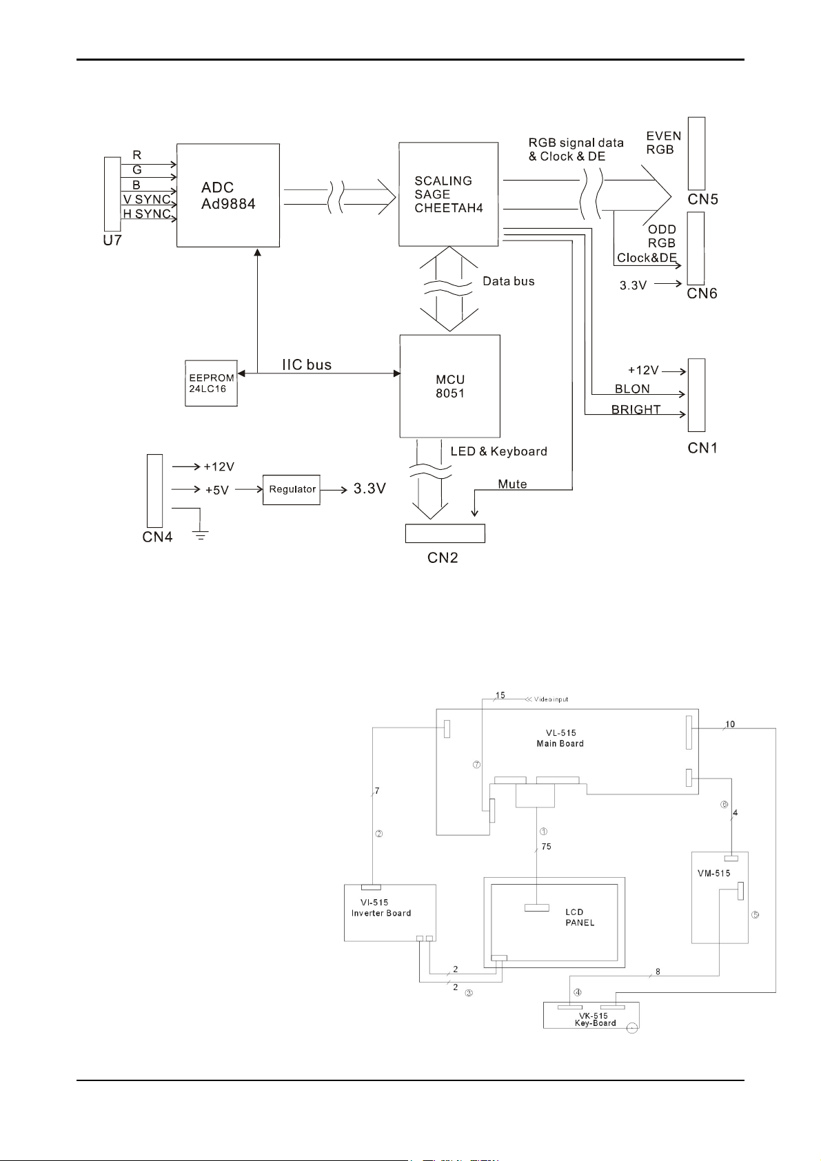
VL-515 DISPLAY CONTROL BOARD
Description
The VL-515 display control board is designed to directly convert the R.G.B signals from VGA
Card D sub-port to optimum LCD timing signals so as to construct a high display quality LCD
monitor.
Features
•
On board sage chip to detect display timings and control user functions.
• Using sage chip to convert R.G.B signals to digital timing
• Using sage chip to offer full screen expansion function on non-XGA mode (Auto-Zoom).
• Support VESA DPMS function.
• Support DDC2B functions.
• DC/DC CNT CKT from VM515 to Supply +5V and 3.3V Sources.
Block Diagram (Control CKT)
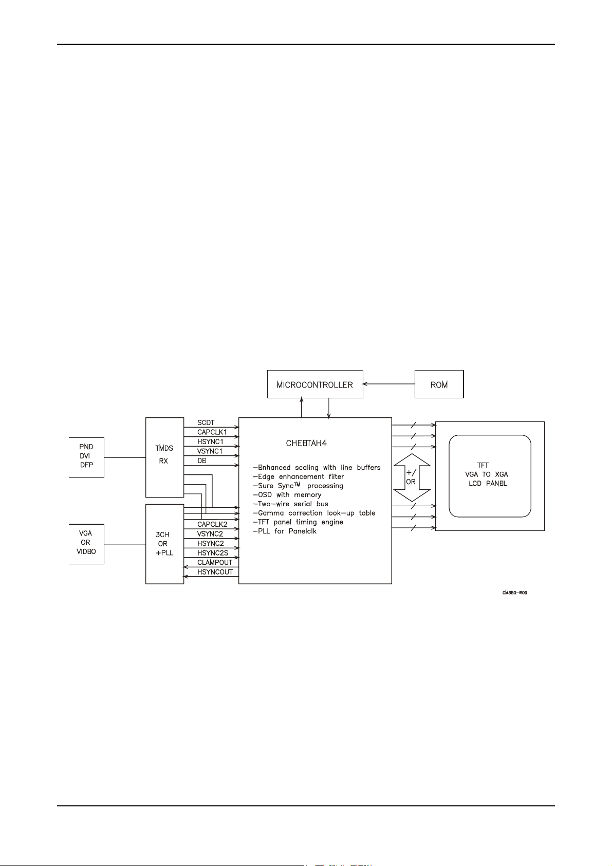
DC-DC
Sage Operation
TheCheetah4 is a single-chip flat panel display controller that provides the ideal interface
between industry-standard digital graphics controllers and a wide variety of LCD panels.
For conversion of input VGA signals to higher resolution outputs, the Cheetah4 uses a
sophisticated scaling algorithm that accepts programmable parameters for horizontal and
vertical interpolation or replication. A highly intelligent filter is employed to dynamically
enhance pixels to offer crisp text images and smooth graphics. The result is an appropriately
sized image with sharp text and clear graphics that takes full advantage of LCD digital
technology. Sage’s SureSync technology extracts accurate information about the resolution and
refresh rate of the input signal and synchronizes to it. Mode changes and sync losses are
10
Page 11
automatically noted and adapted to. Sure-Sync allows Cheetah4 to generate very high quality
output by providing the chip with clean, crisp input signals.
The Cheetah4 contains on-chip line buffers to upscale an image, without the need for external
frame buffer memory.
On-chip gamma correction lookup tables (color translation memories) are used to enable user
programmable brightness, contrast, and gamma correction control. By color-mapping input
RGB data, the user gains full control of the picture quality of the output panel data.
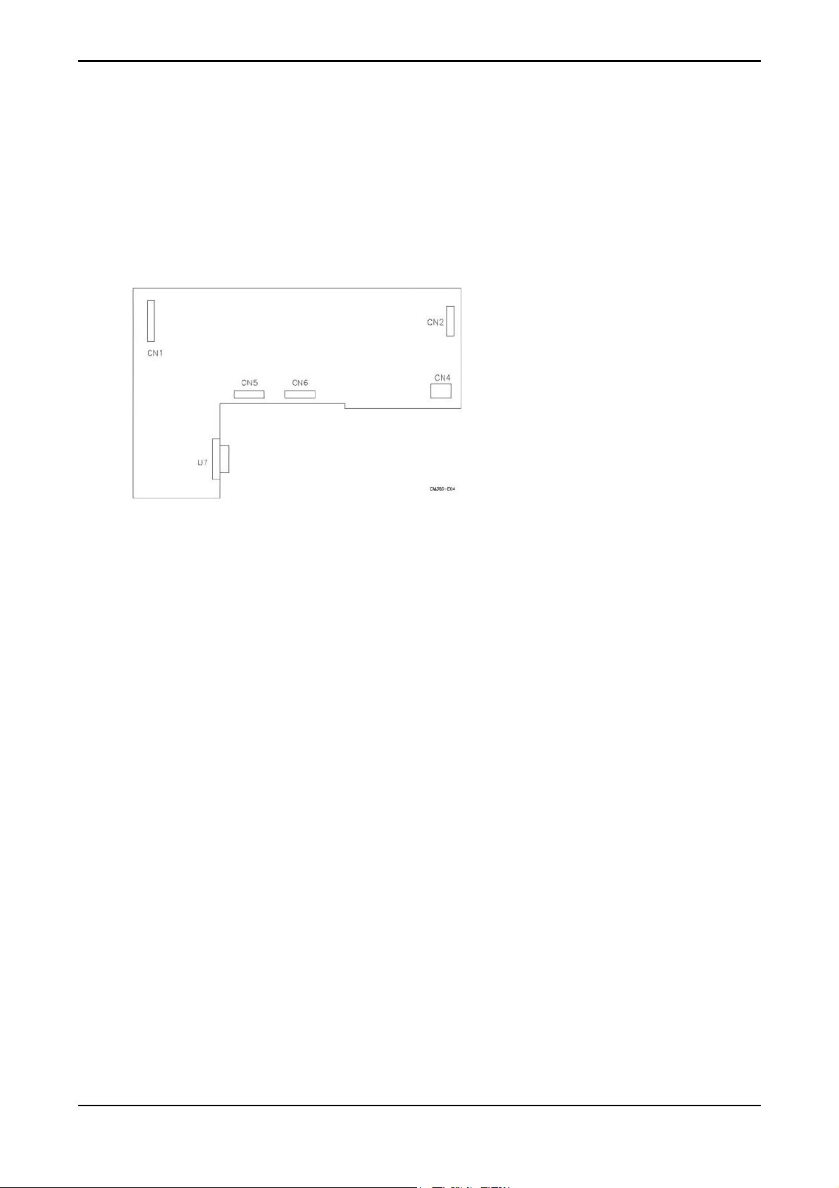
Connector Locations
Connector Type
Location Type Maker Number of pins
U7 DZ11A91-L8 P1.524 FEMALE 15
CN1 96113-0703 E&T 7
CN2 96113-1003 E&T 10
CN4 S4B-XH-A JST 4
CN5 98210-3011 E&T 30
CN6 98210-4511 E&T 45
Connector pin assignment
CN2
Pin No. Signal Comment
1 MUTE Volume adjust power input
2 LED-Y Power saving mode
3 LED-G Monitor is ON
4 GND GND
5 KEY-UP Function select counter-clockwise key
6 KEY-DOWN Function select counter-clockwise key
7 KEY-R Adjust up key
8 KEY-L Adjust down key
9 KEY-POWER Power ON/OFF key
11
Page 12

CN4
CN5
10 GND GND
Pin No. Signal Comment
1 12 VCC 12 VCC Power Input
2 5 VCC 5 VCC Power Input
3 GND GND
4 GND GND
Terminal No. Symbol Function
1 GND Ground
2 BE7 BLUE DATA B7 (MSB) EVEN
3 BE6 BLUE DATA B6 EVEN
4 BE5 BLUE DATA B5 EVEN
5 BE4 BLUE DATA B4 EVEN
6 GND Ground
7 BE3 BLUE DATA B3 EVEN
8 BE2 BLUE DATA B2 EVEN
9 BE1 BLUE DATA B1 EVEN
10 BE0 BLUE DATA B0 EVEN
11 GND GROUND
12 GE7 GREEN DATA G7 (MSB) EVEN
13 GE6 GREEN DATA 6 EVEN
14 GE5 GREEN DATA G5 EVEN
15 GE4 GREEN DATA G4 EVEN
16 GND GROUND
17 GE3 GREEN DATA G3 EVEN
18 GE2 GREEN DATA G2 EVEN
19 GE1 GREEN DATA G1 (LSB) EVEN
20 GE0 GREEN DATA G0 (LSB) EVEN
21 GND GROUND
22 RE7 RED DATA R7(MSB) EVEN
23 RE6 RED DATA R6 EVEN
24 RE5 RED DATA R5 EVEN
25 RE4 RED DATA R4 EVEN
26 GND GROUND
12
Page 13

CN1
27 RE3 RED DATA R3 EVEN
28 RE2 RED DATA R2 EVEN
29 RE1 RED DATA R1 EVEN
30 RE4 RED DATA R0 (LSB) EVEN
Pin No. Signal Comment
1 12 VCC Inverter Power Input.
U7
2 12 V
Inverter Power Input.
CC
3 GND GND
4 GND GND
5 BLON Bright Light ON/OFF high active.
6 5 V
Inverter Power Input.
CC
7 BRIGHT Brightness Adjustment. (0-5V)
Pin No. Signal Comment
1 R-Video Red Video Input.
2 G-Video Green Video Input.
3 B-Video Blue Video Input.
4 N. C.
5 PCDETECT PCDETECT Input.
6 Ground Ground.
7 Ground Ground.
8 Ground Ground
9 5VCC DDC Power Input.
10 Ground Ground.
11 NC
12 SDA DDC 1/2B
13 HS Horizontal Sync Input.
14 VS Vertical Sync Input.
15 SCL DDC 2B
13
Page 14

VK-515 Control Panel and Audio Board
Description
The VK-515 is designed to offer a user interfaced control panel which passes and receives
signals to and from VL-515 display control board. Also there is a stereo audio amplifier to
drive a pair of speakers. When in power saving mode the audio circuit can be turned off by the
control signal from the VL-515 board.
Connector and Switch Locations
Connector type
Location Type Maker Number of pins
J1 96113-0813 E&T 8
J2 SCJ-0348-C SC 9
J3 87502-0200 ACES 2
J4 87502-0200 ACES 2
J5 96113-1013 E&T 10
Connector pin Assignment
J1
Pin No. Signal Purpose
1 VOL Audio Volume Adjust
2,5,8 GND GND
3 OUTL - Left side audio signal
4 OUTL + Left side audio signal
6 OUTL - Right side audio signal
7 OUTL + Right side audio signal
J5
Pin No. Signal Purpose
1 MUTE Volume adjust power input.
2 LED-Y Power saving mode.
3 LED-G Monitor on mode.
4,10 GND
14
Page 15

5 KEY-UP Function select up to VL-515
6 KEY-DOWN Function select down to VL-515
7 KEY-R Function select right to VL-515
8 KEY-L Function select left to VL-515
9 KEY-PWR Power ON/OFF signal to VL-515
J3 and J4
Pin No. Signal Comment
1 LO (RO) Speaker out
2 OUTL - (OUTR-) Speaker out
J2
Pin No. Signal I/O Comment
1 GND Ground
2 LI 2 Earphone out L
3 RI 2 Earphone out R
4 LI 1 Earphone out L
5 LO Speaker out L
6 NC No connector
7 RI 1 Earphone out R
8 RO Speaker out R
Switch definition
Location Definition
S1 Power ON/OFF
S2 Function select by clockwise direction
S3 Function select by counter-clockwise direction
S4 Adjust up
S5 Adjust down
LED definition
Location Definition
D1 Green for ON mode; Off for DC power off; Yellow for stand by; suspend;
off mode.
15
Page 16

Variable resistor
VR1:Volume control, clockwise for increasing; counter-clockwise for decreasing
Electrical characteristics (T
amb
=25
°°°°
)
Audio amplifier (Use Panasonic VP-7723A Audio Analyzor).
Item Audio Input Freq. Spec. Comment
Min. Typ. Max.
Input Voltage(V) 11.4 12 12.6
Input Current(mA) 500 800
Audio Voltage Gain 500mVrms 1KHz 14dB
Frequency Response 100mVrms 50Hz~20KHz -3dB +3dB
Signaal to Noise ratio 500mVrms 1KHz -70dB
Cross talk 100mVrms 1KHz -60dB
Distortion 500mVrms 1KHz 1%
Output Watt. 500mVrms 1KHz 0.5W
Volume Control Analog
VM-515 POWER and AUDIO
Major Specification
Input voltage: 12V±5% from adapter
Volume Max.,load 8 Ω
Volume Max.,load 8 Ω
Volume Max.,load 8 Ω
Volume Max.,load 8 Ω
Volume Max.,load 8 Ω
Volume Max.,load 8 Ω
Output:
ITEM Output Voltage Max Load. Min Load Tolerance Ripple & Noise(max)
VCC +5.1V 1.9A 0.19A ±5% 150mVpp
Description
The VM-515 is designed to supply the power to the VL-515 display control board. Under the
control of VL-515, it can run into power saving mode thereby conserving the power of the
whole monitor.
Efficiency:
80%min. at Maximum Load.
16
Page 17

Connector Locations
Connector type
Location Type Maker Number of pins
J801 DC-IN SC 2
J802 B4B-XH-A JST 4
J2 96113-0803 E&T 8
J3 SCJ-0345-1-X-S SCJ 3
Connector pin Assignment
J801 DC 12V Input
Pin No Signal Comment
Pin 1 +12V From adapter output cable
Pin 2 GND From adapter output cable
J802 FOR I/F CKT
Pin No Signal Comment
Pin 1 +12V From adapter +12V power
Pin 2 +5.1V Supply for I/F CKT
Pin 3, 4 GND GND
J2 FOR K/B SPEAKER
Pin No Signal Comment
Pin 1 VoL Adjustment audio volume.
Pin 2, 5, 8 GND GND
Pin 3 OUTL - Audio output L -
Pin 4 OUTL + Audio output L +
Pin 6 OUTR - Audio output R -
Pin 7 OUTR + Audio output R +
17
Page 18

J3 AUDIO INPUT
Pin No Signal Comment
Pin 1 GND GND
Pin 2 IN-R Audio input R
Pin 3 IN-L Audio input L
VI-515 INVERTER BOARD
Description
The VI-515 Inverter board is designed for lighting up the back-lights of LCD module.
Electrical characteristics
MIN. TYP. MAX. COMMENT
INPUT VOLTAGE 11.4V 12V 12.6V
INPUT CURRENT -------- 0.85A 1A
NO LOAD BACKLIGHT
VOLTAGE
LAMP CURRENT 3mA rms. 6mA rms. 7mArms
DRIVING FREQUENCY 40KHz 45KHz 50KHz
EFFICIENCY -------- 75% -------- Vin = 12V
Operating Life Time 50,000 ------- -------- Hours (del)
-------- 640V rms. --------
Vin=12V MAX.
BRIGHTNESS
Note:
Life time(Hr) can be defined as the time in which it continues to operate under the
condition:
Ta=25±3°C, IL=6.0mA(rms) and fL=30 KHz until one of the following events occurs:
1. When the brightness becomes 50% above
2. When the startup voltage (Vs) at 0°C becomes higher than the maximal value of Vs
specified above
18
Page 19

Connector locations
Connector pin Assignment
P901
Pin No. Signal Comment
1,2 BP+ Power from VL-515
3,4 GND
5 BLT_ON Back-light ON/OFF control , high active(3.3V)
6 +5VS +5VS
7 BRITE BRITE Brightness (0-5V)control from VL-515
5V for min. brightness
P920 & P960
Pin No. Signal Comment
1 LV Low voltage (common)
2 HV High voltage for lamp
19
Page 20

CIRCUIT DESCRIPTION
Micro-Controller Circuit
The U2 (MX10 F MAXD0C) is a system controller.
The Y1 is 14.318MHz XTAL.
Plug and Play Circuit
Plug and play allows the serial communication of host PC and peripherals offering minimal
configurations to end users. This monitor supports DDC2B communication protocol.
SDATA and VCLK are input to U9 (24LC21) and U4 (24LC16).
System Clock
The U1 (14.318MHz XTAL) supports U5 (Sage) reference clock.
Image Engine (Zoom)
The U5 (Sage) is an image engine that has the following functions:
• The Sage is a IFM (Input Format Measurement)
• The Sage is a high quality scalar chip.
Power Regulator
• The U12 (PJ1084) is 5A linear regulator that transfer input voltage from 5V to 3.3V
supports U5.
• The U10 (AME8800) is 300Ma linear regulator that transfer voltage from 5V to 3.3V
supports U6.
20
Page 21

Introduction
Front Panel Control and Led
Front Panel Controls
Item Control Function
1 Power Switch Turns the monitor on and off.
2 Power LED 1. Green indicates monitor is turned on.
2. Yellow indicates DC power off.
3. Amber indicates stand-by, suspend, off mode.
3
Function Button Launches OSD function menu circularly
4
5 Plus Button Selects and adjusts the functions
6 Minus Button Selects and adjusts the functions
21
Page 22

Rear Panel connector Input Signals
Rear Panel Cable and Connector
Item Cable / Connector Function
1
2
3
Signal Connector Connects the video cable
Power Connector Connects the adapter cable
Audio connector Connects the audio cable
22
Page 23

TROUBLESHOOTING
Main Procedure
23
Page 24

Power Circuit Troubleshooting
24
Page 25

Backlights Troubleshooting
25
Page 26

Performance Troubleshooting
26
Page 27

Function Troubleshooting
27
Page 28

A
12
12
C20
C19
+
22uF/35V
4 4
3 3
3.3V_VDD
12
12
12
R24
R23
2 2
1 1
4.7K
CREFCLK
4.7K
CREFCLK
C95
10pF
B[0..7]
G[0..7]
R[0..7]
VSYNC_ASIC
HSYNC_ASIC
R25
4.7K
R70 22
1 2
12
IPIXCLK
PLLHSYNC
MCAD[0..7]
MCA8
MCALE
MCWR#
MCRD#
MCINT
RESET
C96
10pF
B[0..7]
G[0..7]
R[0..7]
12
B7
B6
B5
B4
B3
B2
B1
B0
G7
G6
G5
G4
G3
G2
G1
G0
R7
R6
R5
R4
R3
R2
R1
R0
IPIXCLK
VSYNC_ASIC
HSYNC_ASIC
PLLHSYNC
MCAD0
MCAD1
MCAD2
MCAD3
MCAD4
MCAD5
MCAD6
MCAD7
MCA8
MCALE
MCWR#
MCRD#
MCINT
RESET
R31 20K
12
R30
75
12
C35
0.01uF
133
131
130
129
128
127
126
125
141
140
139
138
137
136
135
134
7
6
5
4
3
2
143
142
121
122
123
124
119
16
12
11
10
9
8
103
104
105
106
107
108
109
110
111
113
112
115
114
102
116
117
118
100
99
93
88
89
97
12
96
U5
CHEETAH4
DBLUE7
DBLUE6
DBLUE5
DBLUE4
DBLUE3
DBLUE2
DBLUE1
DBLUE0
DGREEN7
DGREEN6
DGREEN5
DGREEN4
DGREEN3
DGREEN2
DGREEN1
DGREEN0
DRED7
DRED6
DRED5
DRED4
DRED3
DRED2
DRED1
DRED0
CAPCLK1
VSYNC1
HSYNC1
DE
SCDT
CAPCLK2
VSYNC2
VS2
HSYNC2
HS2
SHSYNC2
SHS
CLAMPO
HSYNCO
MCAD0
MCAD1
MCAD2
MCAD3
MCAD4
MCAD5
MCAD6
MCAD7
MCA8
CHIPSELECT
MCALE
MCWR
MCRD
MCINT
RESET
SCL
DDC
SDA
REFCLK
PLLEN
PANELCLK
XTALIN
XTALOUT
PLL_VCOIN
PLL_CPOUT
0.01uF
INPUT DIGITAL INTERFACE
CHANNEL#1
INPUT TIMING/SYNC
CAPCLK2
CHANNEL#2
INPUT TIMING/SYNC
PLL/CLOCKS
B
L2 BLM21P300S
RC0805D
C21
0.1uF
98
VDD_PCLK
12
72
1444812012436445873
VDDIC1
VDDIC2
VDDIC3
VDDIC4
POWER
VDDO1
VDDO2
CHEETAH3-D
CHEETAH4
uC INTERFACE
GROUND
VSSC3
VSSO5
VSSO6
VSSI2
VSSC2
VSSO7
GND_PCLK
VSSC1
VSSI1
VSSO1
VSSO4
VSSO3
VSSO2
95
1718195440
30
6678909192
*All Res. and Cap. is 0603.
VSSC4
101
132
3.3V_VDD
84
VDDO3
VDDO4
VDDO5
VDDO6
VDDO7
NO CONNECT
94
12
TEST2
TEST1
PLLTEST
15
14
C22
0.1uF
C
12
12
12
12
12
12
12
12
12
C23
0.1uF
C24
C25
0.1uF
C26
0.1uF
0.1uF
20
PDATA0
21
PDATA1
22
PDATA2
23
PDATA3
25
PDATA4
26
PDATA5
27
PDATA6
28
PDATA7
29
PDATA8
31
PDATA9
32
PDATA10
33
PDATA11
34
PDATA12
35
PDATA13
37
PDATA14
38
PDATA15
39
PDATA16
41
PDATA17
42
PDATA18
43
PDATA19
45
PDATA20
46
PDATA21
47
PDATA22
49
PDATA23
50
PDATA24
51
PDATA25
52
PDATA26
53
PDATA27
55
PDATA28
FLAT PANEL INTERFACE
PDATA29
PDATA30
PDATA31
PDATA32
PDATA33
PDATA34
PDATA35
PDATA36
PDATA37
PDATA38
PDATA39
PDATA40
PDATA41
PDATA42
PDATA43
PDATA44
PDATA45
PDATA46
PDATA47
PSHFCLK
PHSYNC
PVSYNC
PENVDD
PENBKL
PWM0
PWM1
PDE
56
57
59
60
61
62
63
64
65
67
68
69
70
71
74
75
76
77
80
79
81
82
83
85
86
87
13
C27
0.1uF
PDATA0
PDATA1
PDATA2
PDATA3
PDATA4
PDATA5
PDATA6
PDATA7
PDATA8
PDATA9
PDATA10
PDATA11
PDATA12
PDATA13
PDATA14
PDATA15
PDATA16
PDATA17
PDATA18
PDATA19
PDATA20
PDATA21
PDATA22
PDATA23
PDATA24
PDATA25
PDATA26
PDATA27
PDATA28
PDATA29
PDATA30
PDATA31
PDATA32
PDATA33
PDATA34
PDATA35
PDATA36
PDATA37
PDATA38
PDATA39
PDATA40
PDATA41
PDATA42
PDATA43
PDATA44
PDATA45
PDATA46
PDATA47
PSHFCLK
PDE
PHSYNC
PVSYNC
PANEL_VCTL
BLON
PWM0
PWM1
C28
0.1uF
4 5
3
2
1
4 5
3
2
1
4 5
3
2
1
4 5
3
2
1
4 5
3
2
1
4 5
3
2
1
C29
0.1uF
RP1 22
RP3 22
RP5 22
RP7 22
RP9 22
RP11 22
PANEL_VCTL
BLON
C30
0.1uF
6
7
8
RP2 22
4 5
3
2
1
6
7
8
RP4 22
4 5
3
2
1
6
7
8
RP6 22
4 5
3
2
1
6
7
8
RP8 22
4 5
3
2
1
6
7
8
RP10 22
4 5
3
2
1
6
7
8
RP12 22
4 5
3
2
1
C31
0.1uF
6
7
8
6
7
8
6
7
8
6
7
8
6
7
8
6
7
8
12
ODD_R0
ODD_R1
ODD_R2
ODD_R3
ODD_R4
ODD_R5
ODD_R6
ODD_R7
ODD_G0
ODD_G1
ODD_G2
ODD_G3
ODD_G4
ODD_G5
ODD_G6
ODD_G7
ODD_B0
ODD_B1
ODD_B2
ODD_B3
ODD_B4
ODD_B5
ODD_B6
ODD_B7
EVEN_R0
EVEN_R1
EVEN_R2
EVEN_R3
EVEN_R4
EVEN_R5
EVEN_R6
EVEN_R7
EVEN_G0
EVEN_G1
EVEN_G2
EVEN_G3
EVEN_G4
EVEN_G5
EVEN_G6
EVEN_G7
EVEN_B0
EVEN_B1
EVEN_B2
EVEN_B3
EVEN_B4
EVEN_B5
EVEN_B6
EVEN_B7
Del R26,R27,R28,R29,C34,Q4
C32
0.1uF
R69 22
4 5
3
2
1
D
+
RP13 22
C33
22uF/35V
ODD_R[0..7]
ODD_G[0..7]
ODD_B[0..7]
EVEN_R[0..7]
EVEN_G[0..7]
EVEN_B[0..7]
12
6
7
8
MUTEPWM0
LCM35H02 RP14~RP19 use 22 ohm
LCM35H03 RP1~RP13 use 120 ohm
ODD_R[0..7]
ODD_G[0..7]
ODD_B[0..7]
EVEN_R[0..7]
EVEN_G[0..7]
EVEN_B[0..7]
SHFCLK
DE
LHSYNC
LVSYNC
MUTE
PWM1
SHFCLK
DE
LHSYNC
LVSYNC
5VCC
R32 10K
1 2
22K
2
22K
R33 20K
1 2
Q5
DTC124EK
1 3
E
3
COLLECTOR
DTC124EK
SOT-23B
2
1
BASE
EMITTER
3
COLLECTOR
2SC2411K
SOT-23B
2
1
BASE
EMITTER
BRIGHT
BRIGHT
+
C36
4.7uF/35V
Layout
change part
Del R34,R35
Title
SCHEMATIC, CTRL BD. VL-515
Size Document Number Rev
A3
401A26
Date: Sheet
A
B
C
D
Friday, December 01, 2000
E
15
1H
of
Page 29

1
2
3
4
5
6
7
8
5VCC
12
Fn [<-]
Fn [->]
Value [+]
Value [-]
Power
C1 0.1uF
1 2
U2
35
EA/VP
21
XTAL1
20
XTAL2
10
RESET
22
VSS
14
INT0
15
INT1
16
T0
17
T1
2
P1.0
3
P1.1
4
P1.2
5
P1.3
6
P1.4
7
P1.5
8
P1.6
9
P1.7
5VCC
44
VCC
C2 0.1uF
1 2
P0.0
P0.1
P0.2
P0.3
P0.4
P0.5
P0.6
P0.7
P2.0
P2.1
P2.2
P2.3
P2.4
P2.5
P2.6
P2.7
RD
WR
PSEN
ALE/P
TXD
RXD
8051
PLCC-44
EXTERNAL
EEPROM
MCAD[0..7]
U1 74HCT373#
MCAD0
43
MCAD1
42
MCAD2
41
MCAD3
40
MCAD4
39
MCAD5
38
MCAD6
37
MCAD7
36
MCA8
24
MCA9
25
MCA10
26
MCA11
27
MCA12
28
MCA13
29
MCA14
30
MCA15
31
MCRD#
19
MCWR#
18
PSEN#
32
MCALE
33
TXD
13
RXD
11
MCA8
MCRD#
MCWR#
MCALE
MCA8
MCAD0
MCAD1
MCAD2
MCAD3
MCAD4
MCAD5
MCAD6
MCAD7
MCALE
C6 0.1uF#
12
5VCC
MCAD7
MCAD6
MCAD5
MCAD4
MCAD3
MCAD2
MCAD1
MCAD0
3
D0
4
D1
7
D2
8
D3
13
D4
14
D5
17
D6
18
D7
5VCC
U3
32 2
VCC A16
30
VCC
31
VCC/WE
22
CE
1
NC
21
D7
20
D6
19
D5
18
D4
17
D3
15
D2
14
D1
13
D0
20
VCC
2
Q0
5
Q1
6
Q2
9
Q3
12
Q4
15
Q5
16
Q6
19
Q7
111
OCG
10
GND
27C010#
24
OE
3
A15
29
A14
28
A13
4
A12
25
A11
23
A10
26
A9
27
A8
5
A7
6
A6
7
A5
8
A4
9
A3
10
A2
11
A1
12
A0
16
GND
5VCC
C3 0.1uF#
1 2
MCA0
MCA1
MCA2
MCA3
MCA4
MCA5
MCA6
MCA7
PSEN#
MCA16
MCA15
MCA14
MCA13
MCA12
MCA11
MCA10
MCA9
MCA8
MCA7
MCA6
MCA5
MCA4
MCA3
MCA2
MCA1
MCA0
MCA[0..15]
INTERNAL EEPROM CHOICE "R1 & R8"
EXTERNAL EEPROM CHOICE "R2 & R9"
C4 22pF
12
C5 22pF
A A
5VCC
12
12
R5
4.7K
SCL
SDA
PCDETECT
SCL
SDA
9884_CTL
PCDETECT
9884_CTL
R6
4.7K
CREFCLK
12
R7
4.7K
R4 rework
CREFCLK
R8 0
1 2
RESET
MCINT
R4 22
1 2
RESET
MCINT
MCU_LEDY
MCU_LEDG
MCA16
12
R1 0
1 2
1 2
R2 0#
Y1
14.318MHzR31M
R9 0#
1 2
5VCC
12
12
12
12
R10
R11
B B
4.7K
12
C7
0.1uF
R12
4.7K
4.7K
12
12
C8
C9
0.1uF
0.1uF
12
R13
R14
4.7K
4.7K
12
12
C10
C11
0.1uF
0.1uF
KEY-UP
KEY-DOWN
KEY-R
KEY-L
KEY-POWER
5VCC
12
1 3
2
BASE
R16
270
Q2
DTC124EK
25Friday, December 01, 2000
3
COLLECTOR
DTC124EK
SOT-23B
LED-G
of
8
1
EMITTER
User mode
EEPROM
5VCC
C12 0.1uF
C15
SDA
SCL
12
R17 422
1 2
12
12
C16
0.1uF
LED-Y
LED-G
KEY-UP
KEY-DOWNKEY-DOWN
KEY-R
KEY-L
KEY-POWER
5
*All Res. and Cap. is 0603 except C15 is 0805.
C C
Inverter Connector Keyboard ConnectorRS232 Debug Connector
CN1
1
2
3
D D
4
5
5VCC
6
7
E&T_96113-0703
1
L1 BLM21P300S
12
C13
0.1uF
R22 1K
RC0805D
+12V_I
12
12
C14
0.1uF
BLON
12
BRIGHT
2
+12V_I
BLON
BRIGHT
MUTE
MUTE
5VCC
4.7uF/10V
C0805D
CN3
TXD
RXD
3
1
2
3
4
HEADER 4
4
U4
8
VCC
5
SDA
6
SCL
4
GND
AT24LC16
SO-8
TEST
A2
A1
A0
CN2
1
2
3
4
5
6
7
8
9
10
E&T_96113-1003
7
3
2
1
LED Pull high
design
5VCC
12
R15
270
LED-Y
MCU_LEDY
22K
2
Q1
22K
DTC124EK
MCU_LEDG
22K
2
22K
1 3
Del R18,R19,C17,C18
Title
SCHEMATIC, CTRL BD. VL-515
Size Document Number Rev
A3
401A26 1H
6
Date: Sheet
7
Page 30

A
ESD parts
ZD1 SLVU2.8#
1
ZD2 SLVU2.8#
1
4 4
ZD3 SLVU2.8#
1
ZD4 SLVU2.8#
1
ZD5 SLVU2.8#
1
Layout
ZD1,ZD2,ZD3,ZD4,ZD5
change to SOT-23
3 3
VSYNC
HSYNC
PC_R
32
PC_G
32
PC_B
32
VSYNC
32
HSYNC
32
1
3
5
9
11
13
7
EDID
VSYNC
DDC_SCL
DDC_SDA
R49
4.7K
12
R50
4.7K
2 2
SLVU2.8
DIO/MA730
12
5V_DDC
DDC_SDA
HSYNC
VSYNC
DDC_SCL
U8
VCC
A1
Y1
A2
Y2
A3
Y3
A4
Y4
A5
Y5
A6
Y6
GND
74AHCT14
12
3
14
2
4
6
8
10
12
5V_DDC
U9
8
VCC
7
VCLK
6
SCL
5
SDA
9
10
11
12
13
14
15
5VCC
VSYNC_ASIC
ADVSYNC
HSYNC_ASIC
ADHSYNC
D1 EC10QS04
1 2
NC
NC
NC
GND
*All Res. and Cap. is 0603.
U7
1
2
3
4
PC_R
1
PC_G
2
PC_B
3
4
PCDETECT
5
6
7
8
ADHSYNC
12
VSYNC_ASIC
HSYNC_ASIC
L3 FCM1608C-300T06
1 2
L4 FCM1608C-300T06
1 2
L5 FCM1608C-300T06
1 2
PCDETECT
L6 FCM1608K-601T02
1 2
C41
22pF
R45 0#
1 2
D2 EC10QS04
12
C45
0.1uF
24LC21A
2 Vin
AME8800AEFT
SOT-89B
2
1
3
Vin
GND
C61
+
10uF/16V
Vout
1 1
5VCC
12
C76
0.1uF
A
U10
APL5883-33DC-TR
2
Vin
3
Vout
GND
1
C62
+
100uF/16V
12
C63
0.01uF
B
1 2
Fred
Fgrn PC_LG
Fblu
1 2
PC_LB
1 2
12
R41
2.2K
5VCC
12
C64
0.1uF
B
PC_LR
R36 75
R37 75
R38 75
12
3.3V_PLL
12
R42
10K
9884_CTL
SDA
SCL
C38
0.047uF
1 2
C39
0.047uF
1 2
C40
0.047uF
1 2
12
R43
75
VPLL
C43
0.039uF
9884_CTL
SDA
SCL
R51 1K
1 2
R52 1K
C97
62pF#
1 2
C98
62pF#
1 2
C99
62pF#
1 2
R39 10K
R40 10K
C42 3900pF
1 2
12
R44
3.3K
C44 0.1uF
1 2
R46 150
R47 150
1 2
R48 150
1 2
12
PC_LG
VPLL
VOP
3.3V_PLL
1 2
12
R55 0#
1 2
R57 10K
12
C48
0.1uF
12
C65
0.1uF
C
VDEC
C37
10uF/16V
124
1285464748494104
VOP
U6
3.3V_VDD
4810111618192325
VDVDVDVDVDVDVDVDVDVDVD
7
R_IN
15
G_IN
22
B_IN
28
12
CLAMP
12
27
CLKINV
40
HSYNC
41
COAST
44
CLKEXT
45
FILT
127
REF_IN
126
REF_OUT
125
/PWRDN
29
SDA
30
SCL
31
A0
32
A1
1
NC
2
NC
3
NC
36
NC
37
NC
38
NC
46
NC
118
SOGOUT
GND
GND
GND
GND
GND
SOGIN
GND
AD9884
GND
GND
GND
GND
GND
5691213141720212426353942474951525363738393
3.3V_PLL
+
114
12033344348
VDD
VDD
VDD
VDD
VDD
VDD
VDD
VDD
GND
GND
GND
GND
GND
GND
GND
GND
GND
GND
GND
103
12
12
12
12
C49
C50
0.1uF
0.1uF
12
12
C66
C67
0.1uF
0.1uF
C
12
C51
C52
0.1uF
0.1uF
12
12
C68
C69
0.1uF
0.1uF
VDEC
12
C53
0.1uF
12
C70
0.1uF
12
12
C71
0.1uF
GND
VPLL
PVD
GND
113
C72
0.1uF
119
12
PVD
GND
PVD
GND
121
C54
0.1uF
PVD
GND
122
D
50
PVD
DATACK
/DATACK
HSOUT
GND
123
12
C73
0.1uF
D
DrA0
DrA1
DrA2
DrA3
DrA4
DrA5
DrA6
DrA7
DrB0
DrB1
DrB2
DrB3
DrB4
DrB5
DrB6
DrB7
DgA0
DgA1
DgA2
DgA3
DgA4
DgA5
DgA6
DgA7
DgB0
DgB1
DgB2
DgB3
DgB4
DgB5
DgB6
DgB7
DbA0
DbA1
DbA2
DbA3
DbA4
DbA5
DbA6
DbA7
DbB0
DbB1
DbB2
DbB3
DbB4
DbB5
DbB6
DbB7
AD9884
MQFP-128
12
C55
0.1uF
E
LCM35H02 RP14~RP19 use 22 ohm
LCM35H03 RP14~RP19 use 120 ohm
RP14
112
111
110
109
108
107
106
105
102
101
100
99
98
97
96
95
92
91
90
89
88
87
86
85
82
81
80
79
78
77
76
75
72
71
70
69
68
67
66
65
62
61
60
59
58
57
56
55
115
116
117
1
2
3
4 5
1
2
3
4 5
1
2
3
4 5
DATACK
R56 22
1 2
22
RP16
22
RP18
22
R53 22
1 2
8
7
6
1
2
3
4 5
RP15
22
8
7
6
1
2
3
4 5
RP17
22
8
7
6
1
2
3
4 5
RP19
22
PLLHSYNC
12
12
C56
0.1uF
12
12
C74
0.1uF
12
C57
C58
0.1uF
0.1uF
C75
Title
0.1uF
SCHEMATIC, CTRL BD. VL-515
Size Document Number Rev
A3
401A26 1H
Date: Sheet
B0
B1
B2
B3
B4
8
B5
7
B6
6
B7
G0
G1
G2
G3
G4
8
G5
7
G6
6
G7
R0
R1
R2
R3
R4
8
R5
7
R6
6
R7
L7
ACB1608H-120T
1 2
12
C46
15pF
PLLHSYNC
12
12
C59
C60
0.1uF
0.1uF
Friday, December 01, 2000
B[0..7]
G[0..7]
R[0..7]
E
12
IPIXCLK
C47
15pF
B[0..7]
G[0..7]
R[0..7]
12
R54
3
of
IPIXCLK
47K
5
Page 31

1
2
3
4
5
6
7
8
Reset
Note: Reset Source Select
12VCC
A A
12
R60
10K#
R58 13K#
1 2
VDD_RST
U11
VCC
Reset
5VCC
C81
+
GND
MAX810_EUR-M
3.3uF/16V#
RESET
12
B B
OPTION
R61
1K#
D3
1N4148#
1 2
RESET
MAX810M
DIO/MA730
1
GND
3
2
1
3
VCC
2
RESET
R59 0
C77 0.1uF
1 2
RESET
12
RESET
5VCC
U14 MCP120-450G-I/TO# KIA7442F#
VCC
GND
Reset
U15 MCP120-450D-I/TO#
Reset
VCC
GND
U16 MCP120-450-I/TT#
Reset
VCC
GND
U17
8
NC
7
NC
6
NC
VDD_RST
1
2
3
RESET
1
VDD_RST
2
3
RESET
1
VDD_RST
2
3
MCP120-450-I/SN#
/RST
VDD
NC
VSSNC
RESET
1
2
3
45
RESET
RESET
RESET
RESET
VDD_RST
MCP120-450G-I/TO
KIA7442F
TO92
1
VCC
MCP120-450D-I/TO
TO92
1
RESET
MCP120-450-I/TT
DIO/MA730
1
RESET
RESET
2
GND
2
VCC
3
GND
3
RESET
3
GND
2
VCC
Power input (+12V,+5V)
CN4
1
2
3
4
ACES_87506_0400
+12V 12VCC
12
C78
C80
C79
0.1uF
5VCC
12
C82
0.1uF
+
100uF/16V
+5V
+
100uF/16V
*All Res. and Cap. is 0603.
12VCC
F1 SMD185
W1
JUMPER WIRE P5
W2
JUMPER WIRE P5
5VCC
+12V_I
+12V_I
OPTION
AME1085DCDT-3
TO-263-3
1
ADJ/GND
2 Vout
2
Vout
3
Vin
C C
REGULATOR +5V->3.3V
U12 APL1084ZC-TR
3.3V_VDD
12
C86
0.1uF
C84
+
1000uF/10V
ADJ/GND
1
23
VoutVin
12
R62
121_1%
12
R63
5VCC 3.3V_VDD
12
C83
+
10uF/16V
D D
C85
0.1uF
200_1%
Title
SCHEMATIC, CTRL BD. VL-515
Size Document Number Rev
A3
401A26
Date: Sheet
1
2
3
4
5
6
Friday, December 01, 2000
7
4
8
1H
5
of
Page 32

A
ODD_R0
RGB DATA ODD
4 4
ODD_R[0..7]
ODD_G[0..7]
ODD_B[0..7]
3 3
EVEN_R[0..7]
EVEN_G[0..7]
EVEN_B[0..7]
LHSYNC
2 2
LVSYNC
SHFCLK
ODD_R[0..7]
ODD_G[0..7]
ODD_B[0..7]
RGB DATA EVEN
EVEN_R[0..7]
EVEN_G[0..7]
EVEN_B[0..7]
L9 ACB1608H-120T#
LHSYNC
LVSYNC
DE
DE
SHFCLK SHFCLK_1
1 2
L10 ACB1608H-120T#
1 2
L11 ACB1608H-120T
1 2
R64 22
1 2
12
C89
10pF
ODD_R1
ODD_R2
ODD_R3
ODD_R4
ODD_R5
ODD_R6
ODD_R7
ODD_G0
ODD_G1
ODD_G2
ODD_G3
ODD_G4
ODD_G5
ODD_G6
ODD_G7
ODD_B0
ODD_B1
ODD_B2
ODD_B3
ODD_B4
ODD_B5
ODD_B6
ODD_B7
EVEN_R0
EVEN_R1
EVEN_R2
EVEN_R3
EVEN_R4
EVEN_R5
EVEN_R6
EVEN_R7
EVEN_G0
EVEN_G1
EVEN_G2
EVEN_G3
EVEN_G4
EVEN_G5
EVEN_G6
EVEN_G7
EVEN_B0
EVEN_B1
EVEN_B2
EVEN_B3
EVEN_B4
EVEN_B5
EVEN_B6
EVEN_B7
C90
10pF
1 2
H_SYNC
V_SYNC
DE_1
Option part number R65,R66,L9,L10,C87,C91,C92
Hannstar panel choice
Choice R65
Less R66,,L9,L10,C87,C91,C92
CPT Panel Set
Choice R66,L9,L10,C87,C91,C92
Less R65
1 1
B
*All Res. and Cap. is 0603 except R65 is 1206.
H_SYNC DE_1
V_SYNC
12
C91
10pF#
12
C92
10pF#
C
CPT Panel connector
EVEN_B7
EVEN_B6
EVEN_B5
EVEN_B4
EVEN_B3
EVEN_B2
EVEN_B1
EVEN_B0
EVEN_G7
EVEN_G6
EVEN_G5
EVEN_G4
EVEN_G3
EVEN_G2
EVEN_G1
EVEN_G0
EVEN_R7
EVEN_R6
EVEN_R5
EVEN_R4
EVEN_R3
EVEN_R2
EVEN_R1
EVEN_R0
3
COLLECTOR
DTC124EK
SOT-23B
12
C93
10pF
2
BASE
1
EMITTER
PANEL POWER
PANEL_VCTL
D
1
2
3
4
5
6
7
8
9
10
11
12
13
14
15
16
17
18
19
20
21
22
23
24
25
26
27
28
29
30
E&T_98210-3011-0.50m
PANEL_VCTL
CN5
GND
BE7
BE6
BE5
BE4
GND
BE3
BE2
BE1
BE0
GND
GE7
GE6
GE5
GE4
GND
GE3
GE2
GE1
GE0
GND
RE7
RE6
RE5
RE4
GND
RE3
RE2
RE1
RE0
PANEL_VDD
3.3V_VDD
12
R65
0
R1206D
L8 STC222B
STS2125
22K
2
22K
5VCC
SHFCLK_1
DE_1
V_SYNC
H_SYNC
ODD_B7
ODD_B6
ODD_B5
ODD_B4
ODD_B3
ODD_B2
ODD_B1
ODD_B0
ODD_G7
ODD_G6
ODD_G5
ODD_G4
ODD_G3
ODD_G2
ODD_G1
ODD_G0
ODD_R7
ODD_R6
ODD_R5
ODD_R4
ODD_R3
ODD_R2
ODD_R1
ODD_R0
C87
+
1000uF/10V#
12
R66
R65 +3.3V use HannStar Panel
0#
R66 +5V use CPT Panel
R1206D
12
R68
4.7K
U13
1
S1
2
S2
3
S3
4 5
GD1
SI9435_SO8
Q6
DTC124EK
E
CN6
1
GND
2
CLK
3
GND
4
DENA
5
GND
6
VD
7
GND
8
HD
9
GND
10
NC
11
GND
12
BO7
13
BO6
14
BO5
15
BO4
16
GND
17
BO3
18
BO2
19
BO1
20
BO0
21
GND
22
GO7
23
GO6
24
GO5
25
GO4
26
GND
27
GO3
28
GO2
29
GO1
30
GO0
31
GND
32
RO7
33
RO6
34
RO5
35
RO4
36
GND
37
RO3
38
RO2
39
RO1
40
RO0
41
VCC
42
VCC
43
12
C88
0.1uF
D4
D3
D2
44
45
8
7
6
TEST
TEST
TEST
E&T_98210-4511-0.50m
PANEL_VDD
C94
+
100uF/16V
1 3
Title
SCHEMATIC, CTRL BD. VL-515
Size Document Number Rev
A3
401A26
A
B
C
D
Date: Sheet
55Friday, December 01, 2000
E
1H
of
Page 33

A
B
C
D
E
SP051005300
T920
5 7
2 8
SP051005300
T960
5 7
2 8
12
4148
D961
470K 1206
R929
C920
220P 3KV
C960
220P 3KV
R922
100K 1%
470K 1206
R961
200K 1%
R921
200K 1%
470K 1206
R931
BAV99L
D920
R920
1.15K 1%
R960
1.15K 1%
BAV99L
D960
123
123
P920
1
CCFL
2
1
CCFL
2
P960
C990
333
R902
*
3
2
VCC
C913
PD1
ND2
ND1
R964
1MC962
5
6
7
8
10U 50V NP
1K 1206
R906
R963
100K
VDD
VADJ
R903
30.9K 1%
R904
57.6K 1%
104
VDD
D990
BAV99L
1
3
84
U990A
LM393
+
1
-
R992
47K
R994
47K
C900
220U/25V low ESR
VREF
C909
104
R993
1K
2
+
R901
1K 1206
R905
10K 1% R930
C903
103
C905
*C902
R907*
R928
22K 1%
VADJ
R995
10K
100K
LM393
84
U990B
5
+
7
6
R996
68K
-
R99A
10K
C991
104
C904
104
Q991
2SC2411K
R999
100K
R915
*
D901
4148
1 2
1
REF
2
OVP
4
SCP
5
ADJ
6
FB
7
CMP
8
GND
U901
OZ962B
VDD
ENA
NDR
PDR
SST
16
15
RT
14
CT
12
11
10
9
VREF
R998
24K
13
R909
64.9K 1%
C907 471
C906
224
C901
104
R910
470K
R911
1 3
22
Q922
2SC2411K
R912
22
Q901
2SA1036K
R926
10K
2
31
Q961
2N7002
2
3
2
1
PG4PD2
PS
NG
NS
U902
SI4559DY
ZD901
RLZ8.2B
R908
330
224
2
1
2
3
4 4
3 3
2 2
1 1
4
5
6
7
P901
E&T 96113-0703
R990
C992
12K R997
104
R991
36K
Title
SCHEMATIC, INVERTER VI-515
Size Document Number Rev
403A26 1F
A3
Date: Sheet of
A
B
C
D
1 1Tuesday, April 25, 2000
E
Page 34

A
4 4
B
C
D
E
Audio board
connector
3 3
MainBoard
connector
2 2
J1
GND
8
OUTR+
7
OUTR-
6
GND
5
OUTL+
4
OUTL-
3
GND
2
VOL
1
E&T_96113-0813
J5
MUTE
1
LED_Y
2
LED_G
3
GND
4
KEY_UP
5
KEY_DOWN
6
KEY_R
7
KEY_L
8
KEY_PWR
9
GND
10
E&T_96113_1013
AGND
S1
PT-002-B2
(S2)
PT-002-B2
(S3)
PT-002-B2
R1
150 1/8W 1%
R2
150 1/8W 1%
(S4)
PT-002-B2
(S5)
PT-002-B2
J2
4 5
LI1 LO
2
LI2
7
RI1
3
RI2
SCJ-0348-C
321
D1
LYG2093 YEL/GRN
GND
NC
RO
6
8
1
AGND
ACES_87502_0200
STRAIGHT/2.5
ACES_87502_0200
STRAIGHT/2.5
R5
100 1/8W 5%
J3
1
2
J4
1
2
VR1
10K
1/20W
10KZ
6
3
5
2
1
4
12
+
-
SP_L1
12
+
-
SP_R1
POWER
(S6)
PT-002-B2
(S7)
PT-002-B2
R4
75 1/8W 1%
VR
1. CM35H & CM87A use S2,S3,S4,S5.
1 1
A
2. CT35H use S6,S7.
35214
6
B
C
D
Title
SCHEMATIC, KEY VK-515
Size Document Number Rev
A3
404A26 1D
Date: Sheet
11Friday, September 22, 2000
E
of
Page 35

A
4 4
B
+12V
C
(To DC-DC)
U2
KA7809
1 3
IN OUT
GND
2
DPAK-G
C2
0.1uF
+
C1
1000uF/16V
D
E
C3
J3
3 3
SCJ-0345-1-X-S
2
5
1
4.7uF/35V
+
+
C4
4.7uF/35V
2
5
1
PH1
2 2
BOTTOM VIEW
C5
0.01uF
R3
1K
C9
0.01uF
R7
1K
R5
100
R6
100
C7
0.1uF
R4
R8
4.7K
4.7K
C6
C10
0.47uF
0.47uF
4
6
2
8
C8
0.1uF
U1
INV1
INV2
VC1
VC2
5
SGND
NC
71410
R1
R2
C11
L2 1mH
VP
PGND
1 1%
1 1%
0.1uF
OUTR+
OUTR-
OUTL+
OUTL-
TDA7053A
16
13
9
+
12
C12
NC/10uF16V
GND
OUTR+
OUTRGND
OUTL+
OUTLGND
VOL
J2
8
7
6
5
4
3
2
1
E&T_96113-0803
1 1
Title
SCHEMATIC, AUDIO VM-515
A
B
C
D
Size Document Number Rev
A3
405A26
Date: Sheet
E
13Tuesday, October 17, 2000
1K
of
Page 36

A
+12V
(To Audio AMP)
B
J802
JST B4B-XH-A
123
4
C
D
E
4 4
R806
5.6k 0603 5%
1N4148
Q804
DTC124EK
*
R813
3 3
L801
STC 471D
1 2
1
2
C801
104 16V
3
C802
4
104 16V
C803
470U/16V LOW-ESR
J801
DC-JACK
2 2
D805
+
C809
10U 50V 4X5.4mm
W803 P5
R801
0.1 2512
+
C804
104 16V
PAD (SHORT)
8
BST
7
IS
6
VCC
U801
AIC1563
R811
150 1206
C806
474 1206
D802
1N4148
SI4800
Q801
1 2
8
7
6
ND1
ND2
ND3
NS1
NS2
NS3
1
2
3
45
NGND4
EC10QS04
1 2
1 2
D801
1N4148
2
C808
821K
C805
821K
R802
33
1
SC
2
SE
3
TC
45
GNDFB
R804
470K
R803
1K
1
3
Q802
2SA1036K
R805
470K
D803
EC10QS04
1 2
R812
150 1206
L802
100UH
D804
ZD801
6.2C
C810
1000U/10V M B P5 L1 5
L803
BLM21P300S
+
R807
3.09K 1%
R808
1K 1%
C807
472K
R809
220
C811
470U/10V M A P3.5 L15
+
C812
104
1 1
Title
SCHEMATIC, AUDIO VM-515
Size Document Number Rev
A3
405A26
A
B
C
D
Date: Sheet
23Wednesday, October 18, 2000
E
1K
of
Page 37

A
+12V
(To Audio AMP)
B
J802
JST B4B-XH-A
123
PAD
4
C
D
E
4 4
F801
SMD(CM870 ONLY) SHORT
C806
1 2
SI4800
Q801
8
ND1
7
ND2
6
ND3
R804
470K
474 1206
NS1
NS2
NS3
NGND4
1 2
D801
1N4148
R803
1K
1
2
3
45
1
2
3
R806
5.6k 0603 5%
C808
821K
C805
821K
D802
1N4148
R802
33
1N4148
Q804
DTC124EK
*
R813
3 3
L801
STC 471D
1 2
J801
DC-JACK
2
1
C801
102
3
C802
4
101
C803
470U/16V LOW-ESR
D805
+
C809
10U 50V 4X5.4mm
W803 P5
R801
0.1 2512
+
C804
104 16V
8
BST
7
IS
6
VCC
U801
AIC1563
1
SC
2
SE
3
TC
45
GNDFB
Q802
2SA1036K
R805
470K
R811
*
EC10QS04
1 2
D803
EC10QS04
1 2
R812
*
D804
L802
56UH
ZD801
6.2C
C810
1000U/10V M B P5 L1 5
L803
BLM21P300S
+
R807
3.09K 1%
R808
1K 1%
C807
472K
R809
220
C811
470U/10V M A P3.5 L15
+
C812
104
2 2
1 1
Title
SCHEMATIC, AUDIO VM-515
FOR CM870 ONLY
A
B
C
D
Size Document Number Rev
A3
405A26 1K
Date: Sheet
33Tuesday, October 17, 2000
of
E
Page 38

38
Page 39

39
Page 40

THE UPDATED PARTS LIST
FOR THIS MODEL IS
AVAILABLE ON ESTA
Page 41

Hitachi, Ltd. Tokyo, Japan
International Sales Division
THE HITACHI ATAGO BUILDING,
No. 15 –12 Nishi Shinbashi, 2 – Chome,
Minato – Ku, Tokyo 105-8430, Japan.
Tel: 03 35022111
HITACHI EUROPE LTD,
Whitebrook Park
Lower Cookham Road
Maidenhead
Berkshire
SL6 8YA
UNITED KINGDOM
Tel: 01628 643000
Fax: 01628 643400
Email: consumer-service@hitachi-eu.com
HITACHI EUROPE GmbH
Munich Office
Dornacher Strasse 3
D-85622 Feldkirchen bei München
GERMANY
Tel: +49-89-991 80-0
Fax: +49-89-991 80-224
Hotline: +49-180-551 25 51 (12ct/min)
Email: HSE-DUS.service@hitachi-eu.com
HITACHI EUROPE srl
Via Tommaso Gulli N.39, 20147
Milano, Italia
ITALY
Tel: +39 02 487861
Tel: +39 02 38073415 Servizio Clienti
Fax: +39 02 48786381/2
Email: customerservice.italy@hitachi-eu.com
HITACHI EUROPE S.A.S
Lyon Office
B.P. 45, 69671 BRON CEDEX
FRANCE
Tel: 04 72 14 29 70
Fax: 04 72 14 29 99
Email: france.consommateur@hitachi-eu.com
HITACH EUROPE AB
Egebækgård
Egebækvej 98
DK-2850 Nærum
DENMARK
Tel: +45 43 43 6050
Fax: +45 43 60 51
Email: csgnor@hitachi-eu.com
Hitachi Europe Ltd
Bergensesteenweg 421
1600 Sint- Pieters-Leeuw
BELGIUM
Tel: +32 2 363 99 01
Fax: +32 2 363 99 00
Email: sofie.van.bom@hitachi-eu.com
www.hitachidigitalmedia.com
HITACHI EUROPE S.A.
364 Kifissias Ave. & 1, Delfon Str.
152 33 Chalandri
Athens
GREECE
Tel: 1-6837200
Fax: 1-6835964
Email: service.hellas@hitachi-eu.com
HITACHI EUROPE S.A.
Gran Via Carlos III, 101- 1
08028 Barcelona
SPAIN
Tel: 93 409 2550
Fax: 93 491 3513
Email: atencion.cliente@hitachi-eu.com
HITACHI Europe AB
Box 77 S-164 94 Kista
SWEDEN
Tel: +46 (0) 8 562 711 00
Fax: +46 (0) 8 562 711 13
Email: csgswe@hitachi-eu.com
HITACHI EUROPE LTD (Norway) AB
STRANDVEIEN 18
1366 Lysaker
NORWAY
Tel: 67 5190 30
Fax: 67 5190 32
Email: csgnor@hitachi-eu.com
HITACHI EUROPE AB
Neopoli / Niemenkatu 73
FIN-15140 Lahti
FINLAND
Tel : +358 3 8858 271
Fax: +358 3 8858 272
Email: csgnor@hitachi-eu.com
HITACHI EUROPE LTD
Na Sychrove 975/8
101 27 Praha 10 – Bohdalec
CZECH REPUBLIC
Tel: +420 267 212 383
Fax: +420 267 212 385
Email: csgnor@hitachi-eu.com
 Loading...