

Page 1
CAUTION:
SERVICE
MANUAL
MANUEL
D'ENTRETIEN
WARTUNGSHANDBUCH
1111111111111111111
11111111111
IIII
HITA-02938
Before
servicing
this
chassis,
it
is
important
that
the
service
technician
read
the
"Safety
Pre-
cautions"
and
"Product
Safety
Notices"
in
this
service
manual.
ATTENTION:
Avant
d'effectuer
l'entretien
du
châssis,
le
technicien
doit
lire
les
"Précautions
de
sécurité"
et
les
"Notices
de
sécurité
du
produit''
présentés
dans
le
présent
manuel.
VORSICHT:
Vor Óffnen des Gehauses hat der Service - lngenieur die "Sicherheitshinweise"
und
"Hinweise
zur
Produktsicherheit''
in
diesem
Wartungshandbuch
zu
lesen.
TECHNICAL SPECIFICATIONS SPECIFICATIONS TECHNIQUES
TV
Standard
...... ······
··B251ines,
Standard
TV
······ ······
··B251ignes,
STANDARD I (UK)
STANDARD:
R-U
B/G/H,
UL',
(Export)
B/G/H
UL':
(Export)
Channel
coverage
.........
UHF
Channels
(UK)
Couverture
de
canaux
· .
.Canaux
UHF
(R-U)
UHFNHF
Hyper
band
(Export)
UHFNHF
Band
hyper
(Export)
Aeríal
input
impedance · ··
· · · · ··. · · ·
··
· 75
ohm
unbalanced
Programme
Selectors · ··Channel
UP/DOWN
buttons
with
70
programme
remate
contrai
CH
direct
input
Power
Consumption
1421
······································39W
2021
······································49W
2121
······································49W
Picture
tubes
1421
.............................
:::,7
cm
type
2021
······ ······ ·················51
cm
type
2121
..................... ········55
cm
type
Mains
Voltage
······ ······ ······220V/240V 50Hz
Fuse
······ ······ ········· ······
..
f"4AH
4.0A
Type
Focusing
· ·
··
· · · ·
··
· · · ·
·· · ··
· · ·········Electra
static
lmpédance
d'entrée
d'antenne · ···
· · · ·
·75
ohm
non
équilibré
Sélecteurs
de
programmes
··
··.
·. -Touches
de
sélection
de
canaux
UP/DOWN
(HAUT/BAS)
avec
70
programmes
Télécommande
Entrée
directe
canal
(CH)
Consommation
propre
1421
....................................
J9W
2021
...................................... 49W
2121
...................................... 49W
Tubes-images
1421
······ ······ ········· ······
··-type
37
cm
2021
······ ······ ········· ······
··-type
51
cm
2121
······ ······ ········· ······
··-type
55
cm
Tension
secteur
............
···220V/240V/50
Hz
Fusible
...........................
Type
F4AH
4.0A
Mise
au
point · ···
· · ·
···
· · · ·
··
··· · ·Eiectrostatique
1997
HITACHI
:,j*~~nJr
;;;.,
.••..
c~t42i_R/T
PA);~BtG
tCLl42iRft
P/SECÁM·L
.•.
cP2021R1T
.
PAL-.BIG·
..
c2t2tRJT·
f8P2121Rff
PAL-BG
..
.
CLl12iR!f
P/SECAM-L
Data
contained
within
this
Service
manual
is
subject
to
alteration
for
improvement.
Les données fournies dans le
présent manuel d'entretien
peu-
vent
faire
l'objet
de
modifications
en
vue
de
perfectionner
le
produit.
Die
in
diesem
Wartungshandbuch
enthaltenen Spezifikationen
kõnnen
sich
zwecks
Verbesserun-
gen
ãndern.
TECHNISCHE
DATEN
Fernsehnorm
. ·
··
....
··.
· · ·
··. ··.
· · ·
·· · ·625
Zeilen,
Fernsehnorm I (nu r GB)
Fernsehnorm
B/G/H,
UL
Kanale
......................
.UHF-Bereich
(GB)
UHF-NHF-/Hyperband-Bereich
(Export)
Antenneneingangsimpedanz
· ·
··
· · · ·
·75
Ohm
unsymmetrisch
Senderwahl
.......................
.AUF/AB-Taste
auf
Fernbedienung
für
70
Sender
Senderdirekteingabe
Leistungsaufnahme
1421
····· ...... ········· ······ ·········
..
J9W
2021
··························· ··········49W
2121
······································49W
Bildrohre
1421
······················ ········ ····37
cm
2021
....................................
51
cm
2121
............ ························55
cm
Netzspannung
....
··
· ·
··
· · ·
·220V-240V,
50Hz
Sicherung
· · · · · · · ·
··
· · · · · · · · · · · · · · · · · · ·
·· · ·F4AH4
OA
Fokusierung
· ·
··
· · · ·
··
· · ·
·· · ··
· · · ·
·Eiektrostatisch
Page 2
HITACHI
SERVI
CE
MANUAL
MANUEL
D'ENTRETIEN
WARTUNGSHANDBUCH
INDEX
SOMMAIRE
English
Français
Safety
instruction
2-UK
2-F
Précautions
de
sécurité
Sicherheitshinweise
TV
operation
supplement
3-UK
3-F
Supplément
sur
le
fonctionnement
du
téléviseur
Erganzung
zur
TV-betriebsanleitung
ldentification
of
functions
on
remate
contrai
4-UK
4-F
Description
des
commandes
de
la
télécommande
Übersicht
über
die
bedienelemente
auf
der
fernhedienung
Tuning
in
the
TV
channels
Programmation
des
canaux
TV
Einstellen
der
TV-Kanale
Connecting
externa!
equipment
Connexion
de
périphériques
Anschluss
externer
gerate
Circuit
description
Description
des
circuits
Schaltkreisbeschreibung
Alignment
instructions
lnstructions
d'alignement
Ausrichtungsinformationen
Block
diagram
Printed
circuit
board
Schematic
diagram
Wave
forms
Electrical
parts
list
Difference
of
parts
for
CRT
Difference
of
parts
for
system
Difference
of
parts
for
option
Mechanical
exploded
view
and
part
list
5-UK
5-F
7-UK
7-F
8-UK
8-F
16-UK
16-F
Common
information
19
20
21
22
23
35
36
37
38
INHALTSVERZETCHNIS
Deutsch
2-D
3-D
4-D
5-D
7-D
8-D
16-D
Page 3
SAFETY
PRECAUTIONS
WARNING : The following precautions should be
observed.
1.
Do
not
instai!,
remove,
or
handle
the
picture tube
in
any
manner unless shatter proof goggles
are
worn.
People
not
so
equipped
should
be
kept
away
while
pic-
ture tubes
are
handled.
Keep
the
picture tube
away
from
the
body
while
handling.
2.
When
service
is
required,
an
isolation transformar
should
be
inserted between the power line
and
the
receiver
before
any
service
is
performed
on
the
chas-
sis.
3.
When
replacing
the
chassis
in
the
cabinet,
ensure
ali
the
protective
devices
are
put
back
in
place.
4.
When
service
is
required, observe
the
originallead
dressing.
Extra
precautions
should
be
taken
to
ensure
correct
lead
dressing
in
the
high
voltage
circuit
area.
5.
Always
use
the
manufacturer's replacement
compo-
nent.
Always replace original spacers
and
maintain
lead
lengths.
Especially criticai components
are
indi-
cated as &
on
the parts list and should not
be
replaced
by
other
makes.
Furthermore,
where a short
circuit
has
occurred, replace those components that
indicate
evidence
of
overheating.
6.
Before
returning a serviced
receiver
to
the
customer,
the
service
technician
must
thoroughly
test
the
unit
to
be
certain
that
it
is
completely
safe
to
operate
without
danger
of
electrical
shock,
and
be
sure
that
no
protec-
tive
device
built
into
the
instrument
by
the
manufactur-
ar
has
become detective,
or
inadvertently damaged
during
servicing.
Therefore,
the
following
checks
are
recommended
for
the
continued
protection
of
the
customers
and
service
techni-
cians.
INSULATION
lnsulation
resistance
should
not
be
less
than
1OM
ohms
at
500V
DC
between
the
main
poles
and
any
accessible
metal
parts.
Also,
no
flashover
or
breakdown
should
occur
during
the
dielectric
strength
test,
applying
3kV
AC
o r
4.25kV
DC
for
two seconds between the
main
poles
and
accessible
metal
parts.
HIGH
VOLT
AGE
High
voltage
should
always
be
kept
at
the
rated
value
of
the
chassis
and
no
higher,
Operating
at
higher
voltages
may
cause
a failure
of
the
picture tube
or
high
voltage
supply,
and
also,
under
certain
circumstances
could
pro-
duce
X-radiation leveis moderately
in
excess
of
design
leveis. The high voltage must
not,
under any circum-
2-UK
stances,
exceed
29kV
on
the
chassis.
X-RADIATION
TUBES : The
primary
source
of
X-radiation
in
this
receiv-
er
is
the picture tube. The tube utilised for the above
mentioned
function
in
this
chassis
is
specially
construct-
ed
to
limit
X-radiation.
For
continued X-radiation protection,
replace
tube
with
the
sarne
type
as
the
original
HITACHI
approved
type.
PRODUCT
SAFETY
NOTICE
Many
electrical
and
mechanical
parts
in
HITACHI
televi-
sion
receivers
have
special
safety
related
characteristics.
These characteristics
are
often
not
evident
from
visual
inspection
nor
can
the
protection
afforded
by
them
nec-
essarily
be
obtained
by
using
replacement
components
rated
for
higher
voltage,
wattage,
etc.
Replacement
parts
which
have
these
special
safety
characteristics
are
iden-
tified
by
marking
with
a &
on
the
schematics
and
the
replacement
parts
list
contained
in
this
service
manual.
Ths
use
of
a substituta replacement component
which
does not have the
sarne
safety characteristics
as
the
HITACHI
recommended
replacement
one,
shown
in
the
parts list
of
this service manual,
may
create electrical
shock,
fire,
X-radiation,
or
other
hazards.
Product Safety
is
continuously under
review,
and
new
instructions
are
issued
from
time
to
time.
For
the
latest
information,
always
consult
the
current
HITACHI
service
manual. A subscription to, or additional copies of
HITACHI
service
manuais
may
be
obtained
ata
nominal
charge
from
your
HITACHI
SALES
CORPORATION.
CE
MARK
Some
of
these
models
may
contain
the
CE
mark
on
the
rating
plate.
This
illustrates
that
the
T.V
contains
parts
that
have
been
specifically
approved
to
provide
electromagnetic
compat-
ibility
to
designated
leveis.
Therefore,
when
replacing
any
part
in
this
T.V.,
please
use
only
the
correct
part
itemized
in
the
parts
list
of
this
service
manual
to
ensure
this
standard
is
maintained.
Also,
take care
to
replace
lead
dressing
to
its
original
state,
as
this
can
also
have a bearing
on
the
electromag-
netic
radiation/immunity.
TUBE
DISCHARGE
The
line
output
stage
can
develop
voltages
in
excess
of
25kV;
if
the
E.H.T.
cap
is
required
to
be
removed,
dis-
charge
the
anode
to
chassis via a
high
value resistor,
prior
to
its
remova!
from
the
tube.
ldúe\lt§!l
Page 4
TV OPERATION SUPPLEMENT
The following pages
are extracted from the
Customer Operating Guide
to
assist Service Engineers
in
TV set
up
3-UK
Page 5
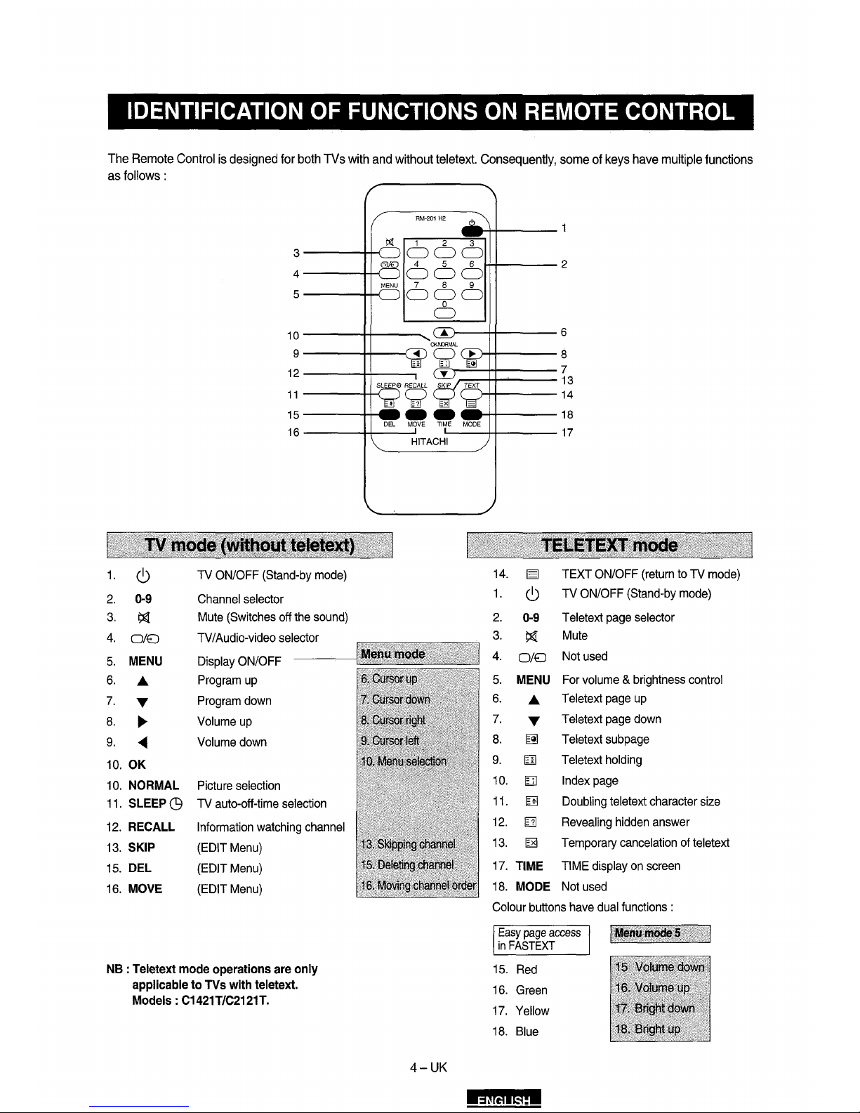
IDENTIFICATION
OF
FUNCTIONS
ON
REMOTE
CONTROL
The Remote Control
is
designed for
both
TVs
with
and
without teletext. Consequently, some
of
keys
have multiple functions
as
follows:
3----+1-{
4----+1-(
5----+1-{
1Q----+~--,
9----1-1---{
12
----+!----.
11----1-1-(
15
----1+--·
16
----+1--....1
1.
ó
2.
0-9
TV
ON/OFF
(Stand-by
mode)
Channel
selector
3.
~
4.
0/8
5.
MENU
6
....
7.
T
8.
...
9.
~
10.
OK
Mute
(Switches
off
the
sound)
TV I Audio-video
selector
Display
ON/OFF
Program
up
Program
down
Volume
up
Volume
down
1
O.
NORMAL
Picture
selection
11.
SLEEP
C9
TV
auto-off-time
selection
12.
RECALL
lnformation
watching
channel
13.
SKIP
(EDIT
Menu)
15.
DEL
(EDIT
Menu)
16.
MOVE
(EDIT
Menu)
NB : Teletext
mode
operations
are
only
applicable
to
TVs
with
teletext.
Models:
C1421T/C2121T.
r----1+----
6
~f-------8
~-,.......;=-++----
7
r=.,....-1H-~--
13
~f-------14
-t-1-f-------
18
.___-Hf-----
17
14.
~
TEXT
ON/OFF
(return
to
TV
mode)
1.
ó
TV
ON/OFF
(Stand-by
mode)
2.
0-9
T
eletext
page
selector
3.
~
Mute
4.
0/8
Not
used
5.
MENU
For
volume & brightness
control
6 .
...
T
eletext
page
up
7.
T
T
eletext
page
down
8.
~
T
eletext
subpage
9.
[;}]
-
Teletext
holding
10.
(I]
I
Index
page
11.
J;] .
Doubling
teletext
character
size
12.
I;]
Revealing
hidden
answer
13.
~
T
emporary
cancelation
of
teletext
17.
TIME
TIME
display
on
screen
18.
MODE
Not
used
Colour
buttons
have
dual
functions
:
Easy
page
access
in
FASTEXT
15.
Red
16.
Green
17.
Yellow
18.
Blue
4-UK
ldM:\11§!1
Page 6
TUNING
lN
THE TV CHANNELS
I·
..
AUTOIVIATIC
TtJNING
$YSTEM
·.···I
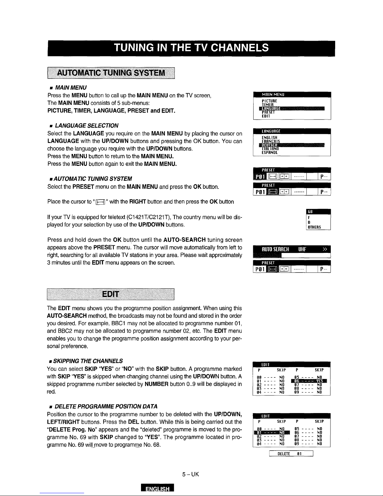
• MA/NMENU
Press
the
MENU
button
to
call
up
the
MAIN
MENU
on
the
TV
screen,
The
MAIN
MENU
consists
of 5 sub-menus:
PICTURE,
TIMER,
LANGUAGE,
PRESET
and
EDIT.
•
LANGUAGE
SELECTION
Select
the
LANGUAGE
you
require
on
the
MAIN
MENU
by
placing
the
cursor
on
LANGUAGE
with
the
UP/DOWN
buttons
and
pressing the
OK
button.
You
can
choose
the
language
you
require
with
the
UP/DOWN
buttons.
Press
the
MENU
button
to
return
to
the
MAIN
MENU.
Press
the
MENU
button
again
to
exit
the
MAIN
MENU.
•
AUTOMATIC
TUNING
SYSTEM
Select
the
PRESET
menu
on
the
MAIN
MENU
and
press
the
OK
button.
Place
the
cursor
to
11
[8]
11
with
the
RIGHT
button
and
then
press
the
OK
button
lf
your
TV
is
equipped
for
teletext
(C1421T/C2121T),
The
country
menu
will
be
dis-
played
for
your
selection
by
use
of
the
UP/DOWN
buttons.
Press
and
hold down the
OK
button until the AUTO-SEARCH tuning screen
appears
above
the
PRESET
menu.
The
cursor
will
move
automatically
from
left
to
right,
searching
for
ali
available
TV
stations
in
your
area.
Please
wait
approximately
3
minutes
until
the
EDIT
menu
appears
on
the
screen.
The
EDIT
menu
shows
you
the
programme
position
assignment.
When
using
this
AUTO-SEARCH
method,
the
broadcasts
may
not
be
found
and
stored
in
the
order
you
desired.
For
example,
BBC1
may
not
be
allocated
to
programme
number
01,
and
BBC2
may
not
be
allocated
to
programme
number
02,
etc.
The
EDIT
menu
enables
you
to
change
the
programme
position
assignment
according
to
your
per-
sonal
preference.
•
SKIPP/NG
THE
CHANNELS
Vou
can
select
SKIP
"YES"
or
"NO"
with
the
SKIP
button. A programme
marked
with
SKIP
"YES"
is
skipped
when
changing
channel
using
the
UP/DOWN
button.
A
skipped
programme
number
selected
by
NUMBER
button 0 .. 9 will
be
displayed
in
red.
•
DELETE
PROGRAMME
POSITION
DATA
Position
the
cursor
to
the
programme
number
to
be
deleted
with
the
UP/DOWN,
LEFT/RIGHT buttons.
Press
the
DEL
button.
While
this
is
being carried
out
the
"DELETE
Prog.
No"
appears
and
the
"deleted"
programme
is
moved
to
the
pro-
gramme
No.
69
with SKIP changed
to
"YES".
The
programme located
in
pro-
gramme
No.
69
wiiLfnove
to
programrn_e
No.
68.
5-UK
IJúdiM!i
MAIN
MENU
PICTUAE
TIMER
lRNGURGE
PAESET
EDil
LANGUAGE
ENGLISH
FRANCA
IS
DEUTSCH
ITALIANO
ESPANOL
RESET
III ED
lcr:JII
------
I
PRESET
I
P--
I
I
P--
I
AUTO
SEARCH
UHF
»
-------~
EDil
p
SKIP
p
SKIP
00
----
NO
05
----
NO
01
----
NO
MH,
n•
02
- - - -
NO
07
----
NO
03
----
NO
08
----
NO
04
----
NO
09
----
NO
EDil
p
SKIP
p
SKIP
00
----
NO
05
----
NO
·~·
~~~-
06
----
NO
02
----
NO
07
----
NO
03
----
NO
08 - - - -
NO
04
----
NO
09
- - - -
NO
DELETE
01
Page 7
TUNING
lN
THE TV CHANNELS
•
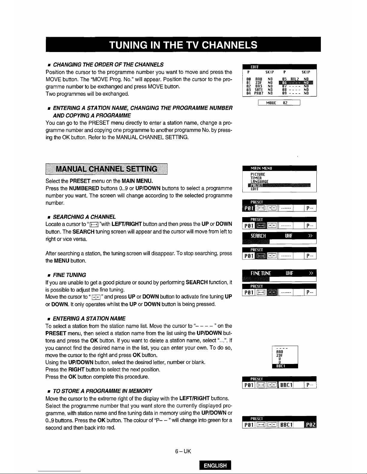
CHANGING
THE
ORDER
OF
THE
CHANNELS
Position
the
cursor
to
the
programme number
you
want to
move
and
press
the
MOVE
button.
The
"MOVE
Prog.
No."
will
appear.
Position
the
cursor
to
the
pro-
gramme
number
to
be
exchanged
and
press
MOVE
button.
Two
programmes
will
be
exchanged.
•
ENTERING A STATION
NAME,
CHANGING
THE
PROGRAMME
NUMBER
ANDCOPWNGAPROGRAMME
You
can
go
to
the
PRESET
menu
directly
to
enter a station
name,
change a pro-
gramme
number
and
copying
one
programme
to
another
programme
No.
by
press-
ing
the
OK
button.
Reter
to
the
MANUAL
CHANNEL
SETTING
.
.
•·····'I\II~Nll~LÇH~N,N~f•.$Elt1N~·
·.• · .....•...
·)
Select
the
PRESET
menu
on
the
MAIN
MENU.
Press
the
NUMBERED
buttons 0 .. 9 or
UP/DOWN
buttons
to
select a programme
number
you
want.
The
screen
will
change
according
to
the
selected
programme
number.
•
SEARCHING A CHANNEL
Locate a cursor
to"
BJ
"with
LEFTIRIGHT
button
and
then
press
the
UP
or
DOWN
button.
The
SEARCH
tuning
screen
will
appear
and
the
cursor
will
move
from
left
to
right
or
vice
versa.
After
searching a station,
the
tuning
screen
will
disappear.
To
stop
searching,
press
the
MENU
button.
•
FINE
TUNING
lf
you
are
unable
to
get a good
picture
or
sound
by
performing
SEARCH
function,
it
is
possible
to
adjust
the
fine
tuning.
Move
the
cursor
to"
EEJ"
and
press
UP
or
DOWN
button
to
activate
fine
tuning
UP
or
DOWN.
lt
only
operates
whilst
the
UP
or
DOWN
button
is
being
pressed.
•
ENTERING A STA
TION
NAME
To
select a station
from
the
station
name
list.
Move
the
cursor
to "-- - - "
on
the
PRESET
menu,
then
select a station
name
from
the
list
using
the
UP/DOWN
but-
tons
and
press
the
OK
button.
lf
you
want
to
delete a station
name,
select
" ...
".
lf
you
cannot
find
the
desired
name
in
the
list,
you
can
enter your
own.
To
do
so,
move
the
cursor
to
the
right
and
press
OK
button.
Using
the
UP/DOWN
button,
select
the
desired
letter,
number
or
blank.
Press
the
RIGHT
button
to
select
the
next
position.
Press
the
OK
button
complete
this
procedure.
•
TO
STORE A PROGRAMME
lN
MEMORY
Move
the
cursor
to
the
extreme
right
of
the
display
with
the
LEFT/RIGHT
buttons.
Select
the
programme number that
you
want
store
the
currently displayed
pro-
gramme,
with
station
name
and
fine
tuning
data
in
memory
using
the
UP/DOWN
or
0
..
9
buttons.
Press
the
OK
button.
The
colou r of
"P-
- "will
change
into
green
for
a
second
and
then
back
into
red.
6-UK
•aua•w=•
EDIT
p
SKIP
00
AAD
NO
01
ZDF
NO
02
BA3
NO
03
SATl
NO
04
PA07
NO
MOUE
MAIN
MENU
PICTURE
TIMER
LANGUAGE
PRESEI
EDIT
p
05
ATL2
MIJí
o7
08
- - - -
09
- - - -
02
PRESET
I
POl
Jlr=IIEEJII
------1
SKIP
NO
:u•
NO
NO
NO
I
P--1
I
P--I
SEARCH
UHF
»
---
PRESET
I
POl,IIIIIIIEEJII
------1
I
P--I
FINETUNE
UHF
»
[[]
F
u
i
P--i
PRESET
11
Page 8
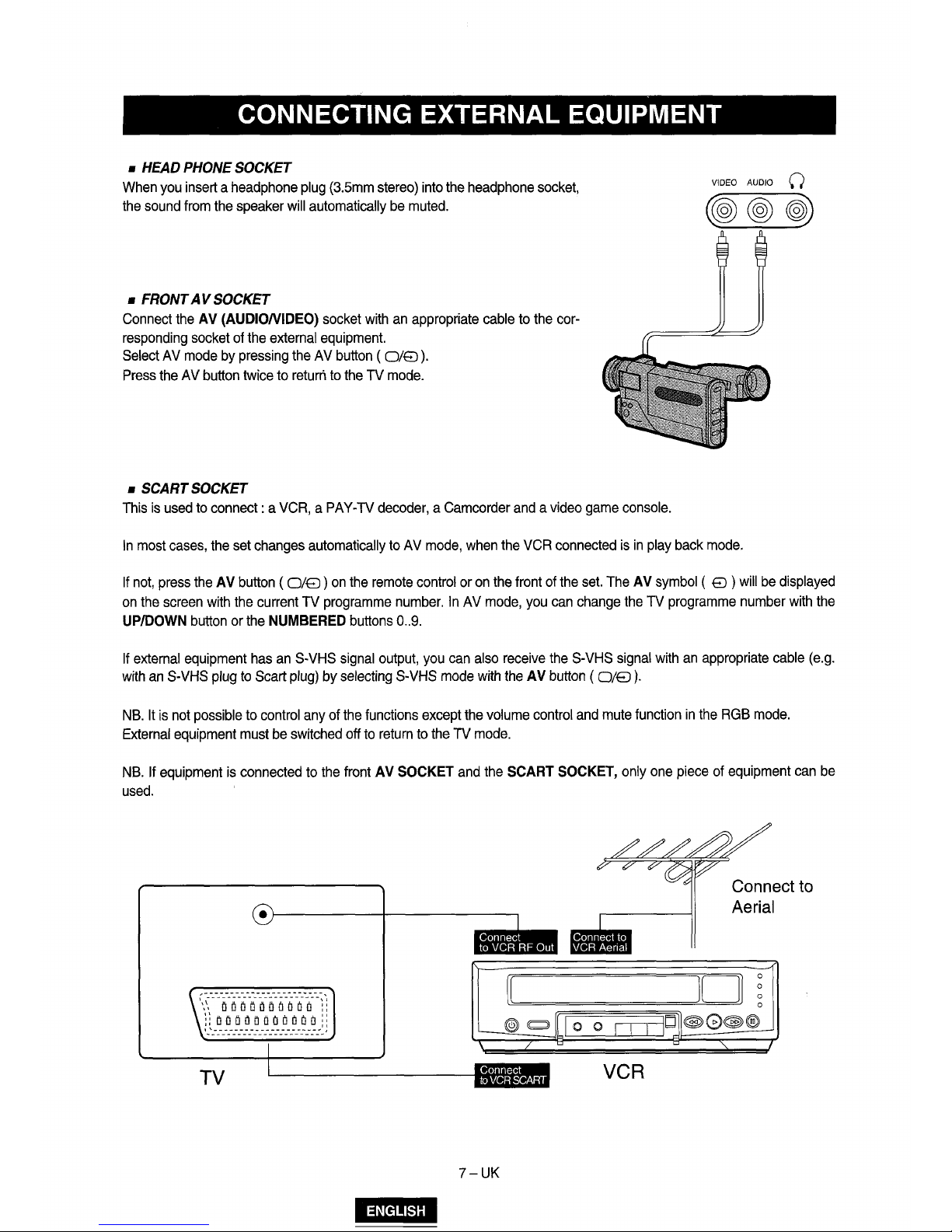
CONNECTING EXTERNAL EQUIPMENT
•
HEAD
PHONE
SOCKET
When
you
inseri a headphone
plug
(3.5mm
stereo)
into
the
headphone
socket,
the
sound
from
the
speaker
will
automatically
be
muted.
•
FRONT
AV
SOCKET
Connect
the
AV
(AUDIONIDEO)
socket
with
an
appropriate
cable
to
the
cor-
responding
socket
of
the
externa!
equipment.
Select
AV
mode
by
pressing
the
AV
button ( 0/8
).
Press
the
AV
button
twice
to
retuni
to
the
TV
mode.
•
SCART
SOCKET
This
is
used
to
connect: a
VCR, a PAY-TV
decoder, a Camcorder
anda
video
game
console.
VIDEO AUDIO
ln
most
cases,
the
set
changes
automatically
to
AV
mode,
when
the
VCR
connected
is
in
play
back
mode.
lf
not,
press
the
AV
button ( 0/8 ) on
the
remote
control
or
on
the
front
of
the
set.
The
AV
symbol
( 8 )
will
be
displayed
on
the
screen
with
the
current
TV
programme
number.
ln
AV
mode,
you
can
change
the
TV
programme
number
with
the
UP/DOWN
button
or
the
NUMBERED
buttons 0 ..
9.
lf
externa!
equipment
has
an
S-VHS
signal
output,
you
can
also
receive
the
S-VHS
signal
with
an
appropriate
cable
(e.g.
with
an
S-VHS
plug
to
Scart
plug)
by
selecting
S-VHS
mode
with
the
AV
button ( 0/8
).
NB.
lt
is
not
possible
to
control
any
of
the
functions
except
the
volume
control
and
mute
function
in
the
RGB
mode.
Externa!
equipment
must
be
switched
off
to
return
to
the
TV
mode.
NB.
lf
equipment
is
connected
to
the
front
AV
SOCKET
and
the
SCART
SOCKET,
only
one
piece
of
equipment
can
be
used.
o I I I
VCR
7-UK
Connect to
Aerial
lDI
~
o
Page 9
• Circuit Description
Vision
IF
amplifier,
AFC,
video
demodulator
The
IF
signal
from
the
tuner
is
fed
through a SAW
filter
to
the
differentiaiiF
input
(pin
48
and
49).
The
first
IF
stage
consists
of 3 AC-coupled
amplifiers
with a total
gain
control
range
of
over
66
dB.
The
reference
carrier
for
the
video
demodulator
is
obtained
by a PLL
carrier
regenerator
(eliminating
notch
filter
compromises,
as
in
reference
tuned
circuits
for
passive
carrier
regeneration).
Only
an
oscillator
coil
is
needed(
pin 3 and
4)
that
can
be
aligned
via
12C-bus
to
the
double
IF
frequency.
The
AFC
information
is
derived
from
the
VCO
control
voltage
of
the
IF-PLL
and
can
be
read
via
12C-bus.
Bit
AFB
toggles
when
the
picture
carrier
is
exactly
at
the
desired
IF
frequency
(=
half
the
aligned
IF-PLL
frequency).
AFA
is
active
in a window
around
this
point.
For
fast
search-tuning
applications
this
window
can
be
increased
by a factor 3 (AFW
bit).
Tuner
A.G.C.
The
automatic
gain
control
(A.G.C.)
circuit
operates
on
top
sync
levei
at
negative
modulated
signals
or
on
peak
white
levei
at
positive
modulation,
selected
by
MOD
bit.
The
tuner
A.G.C.
is
controlled
via
pin
54.
The
tuner
A.G.C.
take
over
point
(T.O.P.)
can
be
set
over a wide
range:
0.8
mVrms
..
80
mVrms
IF
input
signal
amplitude.
The
tuner
AGC
output
may
have
to
operate
above
Vcc
of
TDA837
4.
Therefore
pin
54
is
an
open
collector
output,
that
can
operate
from
0.3
up
to
Vcc+ 1 Volt
(at
> 2
mA
sink
current)
PLL
sound
demodulator
The
IF-video
output
at
pin 6 (2Vpp)
is
fed
through a sound
bandpass
filter
and
connected
to
the
intercarrier
sound
IF
input
pin
1.
An
alignment
free
PLL
tunes
itself
to
the
sound
carrier
and
demodulates
it.
The
non
volume-controlled
front-end
audio
signal
can
be
obtained
from
the
deemphasis
pin
55
(amplitude
300
mVeff).
Source
select
switch
TDA837 4 input
switch
can
select
one
of
the
following
sources
;
pin
13
front-end : CVBS I int
pin
17
:
CVBS 2 ext
pin
11.pin
1 O : Y
s-vhs, C s-vhs
Selected
signal
is
available
at
the
CVBS
output
pin
38,
in
case
of Y /C
input Y +C
are
added.
lt
drives
teletext
and
the
TDA8395
SECAM
add-on.
For
S-VHS
applications,
the
Y,C
input
can
be
selected,
independeht
of
the
CVBS
source
switch.
TDA8374
Y,C
inputs
are
selected,
while
the
source
switch
outputs
CVBS I int
or
CVBS 2 ext
on
CVBS
out.
Horizontal
synchronization
and
protection
The
synchronization
separator
adapts
its
slicing
levei
in
the
middle
between
top-sync
and
black
levei
of
the
CVBS
signal.
The
separated
synchronization
pulses
are
fed
to
the
first
phase
detector
and
to
the
coincidence
detector.
The
fP-1
loop
gain
is
determined
by
the
components
at
pin
43
(C+RC).
The
coincidence
detector
detects
whether
the
horizontalline
oscillator
is
synchronized
to
the
incoming
video.
The
line
oscillator
is a VCO-type,
running
at
twice
the
line
frequency.
lt
is
calibrated
with
the
X-tal
oscillator
frequency
of
the
colou r decoder
and
has a maximum
deviation
of
2%
of
the
nominal
frequency,
so
no
alignment
is
needed.
Calibration
is
done
at
start
up(
the
TDA8374
must
first
know
what
colour
X-tais
are
connected,
bits
XA
and
XB)
and
after
synchronization
loss ( fP-1
coincidence
detector
"Sync
Locked"
bit
SL).
The
second
phase
detector
fP-2
locks
the
phase
of
the
horizontal
driver
pulses
at
output
pin
40
to
the
horizontal
flyback
pulse
at
input
pin
41
.
8-UK
Page 10
This
compensates
for
the
storage
time
of
the
horizontal
deflection
transistor.
The
a>-
2
loop
filter
(C)
is
externally
connected
to
pin
42.
The
horizontal
phase
can
be
given a static
off
set
via
12C-bus
(HSH
"horizontal
shift'')
A
dynamic
correction
is
possible
by
current
feedback
into
the
a>-
2
/oop
fi/ter
capacitar.
To
protect
the
horizontal
deflection
transistor,
the
horizontal
drive
is
switched
off
immediately
when a power
failure
("
Power-On
Reset"
bit
POR)
is
detected.
The
power
failure
may
have
corrupted
the
contents
of
the
internal
data
registers,
so
the
TDA8374
should
be
started
up
again.
The
TDA837 4 has a separate
supply
input
(pin
37)
that
is
only
used
as a clean
supply
vo/tage
for
the
horizontal
oscillator
circuits.
Vertical
synchronization
The
vertical
sawtooth
generator
drives
the
vertical
output.
lt
uses
an
externa/
capacitar
at
pin
51
anda
current
reference
resistor
at
pin
52.
The
TDA8374
vertical
drive
has
differential
current
outputs
for
DC-coupled
vertical
output
stage,
like
the
TDA8356.
At
TDA8356
input
pins I and 2 this
current
is
converted
into a drive
voltage
via a resisto
r
Geometry
processing
With
the
TDA8374
it
is
possible
to
implement
automatic
geometry
a/ignment,
because
ali
parameters
are
adjusted
via
the
12C
bus.
The
deflection
processar
of
the
TDA837 4 offers
the
following
five
contrais;
-
Horizontal
shift
-Vertical
slope.
-
Vertical
amplitude
-Vertical 8-correction
-
vertical
shift
Colou r decoder
The
colour
decoder
contains
an
alignment-free
X-tal
oscillator, a dual
killer
circuit
and
co/our
difference
demodu/ators.
Together
with
the
TDA8395
SECAM
add-on a multi
standard
PAUSECAM/NTSC
decoder
can
be
built
with
automatic
recognition.
Which
standard
can
be
decoded depends
on
the
externa/
Xtals
used.
Two
Xtal
pins
(34and
36)
are
present
so
normally
no
externa/
switching
is
required.
The
I.
C.
must
be
to/d
which
X-tais
are
connected
(bits
XA
and
XB).
This
is
important,
because
the
X-tal
frequency
of
the
colour
decoder
is
also
used
to
calibrate
many
internal
circuits.
The
burst
phase
detector
locks
the
Xtal
oscillator
with
the
chroma
burst
signal.
The
phase
detector
operates
duríng
the
burst
key
períod
only,
to
prevent
dísturbance
of
the
PLL
by
the
chroma
sígnal.
Two
gain
modes
provide:
-
Good
catching
range
when
the
PLL
is
not
Locked.
-
Low
ripple
voltage
and
good
noise
immunity
once
the
PLL
has
locked
The
killer
circuit
switches-off
the
R-Y
and
8-Y
demodulators
at
very
/ow
input
signal
conditions
(chroma
burst
amplitude).
A
hysteresis
prevents
on/off
switching
at
low,
noisy
signals.
Color
standard
pin34 pin35
XA
XB
PAL4.43/SECAM + NTSC-4.43
none
4.43
1
o
PAL4.43/SECAM + NTSC-M
3.58
4.43
1 1
9-UK
Page 11
lntegrated
video
filters
The
TDA8374
has
alignment-free
internalluminance
delay,
chroma
bandpass
and
chroma
trap.
They
are
implemented
as
gyrator
circuits
tuned
by
tracking
to
the
frequency
of
the
chroma
Xtal
oscillator.
The
chroma
trap
in
the Y signal
path
is
by-passed
when
Y/C
input
is
selected
(S-VHS
).
For
SECAM
an
extra
luminance
delay
is
built-in,
for
correct
delay
of
the
luminance
signal.
RGB
output
and
black
current
stabilization
The
colour
difference
signals
(R-Y,
8-Y)
are
matrixed
with
the
luminance
signal
(Y)
to
obtain
the
RGBout
output
signals
(pins
21
,20,29).
ln
the
TDA8374
the
matrix
type
automatically
adapts
to
the
decoded
standard
(NTSC,PAL).
Linear
amplifiers
are
used
to
interface
externa!
RGB
in
signals
(pins
24,25,26)
from
the
SCART
connector.
These
signals
overrule
the
internal
RGB
signals
when
the
data
insertion
pin
26
(FBI)
is
switched
to a levei
between
1.0V
and
3.0V.
The
contrast
and
brightness
control
and
the
peak
white
limiter
operate
on
both
internal
and
externa!
RGB
signals
R,G
and B each
have
their
own,
independent
gain
control
to
compensate
for
the
difference
in
phosphor
efficiencies
of
the
picture
tube:
so
called
''white
point''
adjustment.
The
nominal
amplitude
is
about
2V
black
to
white,
at
nominal
input
signals
and
control
settings.
TDA837 4 has a black
current
stabilization
loop,
that
automatically
adjust
the
black
levei
to
the
cut-off
voltage
of
the
picture
tubes
three
gun
cathodes.
Since
no
current
is
flowing
when
the
voltage
of
the
cattiode
is
equal
to
the
cut-off
voltage
of
the
tube,
the
loop
stabilizes
at a
very
small
gun
current.
•
This
"black
currenf'
of
the
three
guns
is
measured
internally
and
compared
with a reference
current,
to
adjust
the
black
levei
of
RGBout.
The
black
levelloop
is
active
during 4 !ines
at
the
end
of
the
vertical
blanking.
ln
the
first
line
the
leakage
current
is
measured
(max.
acceptable
100
,A).
ln
the
next
three
!ines
the
black
leveis
of
the
three
guns
are
adjusted.
The
nominal
value
of
the
'black
current
is
1 O ,A.
The
ratio
of
the
'black
currents'
for
the 3 guns
tracks
automatically
with
the
white
point
adjustment,
so
the
back-ground
colour
is
the
sarne
as
the
adjusted
white
point.
At
switch-on
of
the
TV
receiver
the
black
current
stabilization
circuit
is
not
yet
active
and
RGBout
are
blanked.
Before
the
first
measurement
pulses
appear,
0.5
sec
delay
ensures
that
the
vertical
deflection
is
active,
so
the
pulses
will
not
be
visible
on
the
screen.
During
the
measuring
!ines
RGBout
will
supply
4V
pulses
to
the
video
output
stages.
The
TDA837 4 waits
until
the
black
current
feedback
input
(pin
18)
exceeds
200
pA,
which
indicates
that
the
picture
tube
has
warmed
up.
Then
the
black
current
stabilization
circuit
is
active.
After a waiting
time
of
about
1.0
sec,
the
blanking
of
RGBout
is
released.
Tuning
The
AFC
information
of
the
TDA837 4 is
not
available
as
an
analogue
voltage.
Automatic
following
(=frequency
tracking,
AFC)
can
be
done
via
the
12C-bus
by
software.
The
TDA837 4 AFC
window
is
typically
80
kHz
wide.
This
value
is
made
higher
than
the
62.5
kHz
tuning
step,
to
prevent
an
automatic
following
loop
from
continuously
adapting
the
tuning
frequency
..
With
this
AFC
window ( ±40
kHz)
the
maximum
tuning
error
is
less
than
62.5
kHz.
For
high
speed
search-tuning-algorithms,
the
AFC
window
can
be
widened
to
240
kHz
via
bit
AFW.
10-UK
Page 12
TDA8395
SECAM
decoder
The
TDA8395
is
an
alignment-free
SECAM
colou r decoder,
including a Cloche
filter,
demodulator
and
line
identification
circuit.
The
Cloche
filter
is a gyrator-capacitor
type.
lts
frequency
is
calibrated
in
the
vertical
retrace
period.
The
calibration
reference(
pin
1 )
is
obtained
from
the
TDA8374
colour
X-tal
oscillator
(pin
33).
Pin 7 is a decoupling
for
the
Cloche
reference.
The
voltage
change
at
this
pin
dueto
leakage
currents
should
be
lower
than
1 O
mV,
during
field
scan,
resulting
in
a
capacitor
of
minimal100
nF.
Pin 8 is
the
reference
capacitor
for
the
PLL.
The
voltage
variation
during
field
scan
at
this
pin
should
be
lower
than 2 mV , resulting
in a capacitor
of
220
nF.
The
sandcastle
input
(pin
15)
is
connected
to
TDA837 4 pin
41
and
is
used
for
generation
of
the
blanking
periods
and
provides
clock
information
for
the
identification
circuit.
The
CVBS
source
select
output
(TDA837 4 pin
38)
supplies
SECAM
chroma
to
pin
16
of
the
TDA8395.
This
is
demodulated
by a PLL
demodulator,
that
uses
the
reference
frequency
at
pin I and a bandgap
reference
to
obtain
the
desired
demodulation
characteristic.
lf
the
digitalline
identification
in
the
TDA8395
detects
SECAM,
pin 1 will
sink a current
of
150
(A
out
of
TDA8374
SECAMref
pin
33.
When
the
TDA8374
has
not
detected
PAL
or
NTSC,
it
will
respond
by
increasing
the
voltage
at
pin
33
from
1.5V
to
5V.
Now
the
TDA837 4 colou r difference
outputs
pin
30
and
29
are
made
high-ohmic
and
the
TDA8395
output
pin 9 and
1 O
are
switched
on.
These
outputs
will
be
disconnected
and
high-ohmic
when
no
SECAM
is
detected
for
two
trame
periods,
the
decoder
will
be
initialized
before
trying
again.
SECAM-L
and
-L:
application
For
SECAM-L
and
L'
the
TDA8374
has
to
be
switched
to
positive
modulation
via
12C-bus
bit
MOD.
SECAM-L'
signals
only
occur
in
VHF
band I and
have
their
picture
and
sound
carrier
interchanged,
compared
to
SECAM-UPAL
channels.
For
SECAM-L'
the
IF
picture
carrier
is
situated
at
34.2
MHz
and
the
AM-sound
carrier
at
40.7MHz.
Therefore
the
IF-PLL
reference
has
to
be
tuned
away
from
38.9
to
34.2
MHz.
This
can
be
done
via
12C-bus
sub-address
15hex
(IF-PLL).
The
AM
sound
output
is
inserted
at
TDA837 4 externa!
audio
input
pin
via
the
SCART
plug.
When
bit
MOD
selects
positive
modulation
for
SECAM-UL',
the
TDA8374
automatically
switches
to
externa!
audio.
Base
band
delay
line
TDA4665
TDA4665
is
an
integrated
double
baseband
delay
line
of
64
~
lt
couples
to
the
TDA837 4 and
TDA8395
without
any
switches
o r
alignments.
The
TDA4665
consist
of
two
main
blocks:
-
Two
delay
!ines
of
64
sec
in
switched
capacitar
technique
-
Internal
clock
generation
of 3 MHz,
line
locked
to
the
sandcastle
pulse
The
TDA4665
operates
according
to
the
mode
demanded
by
the
colou r transmission
standard:
-For
PAL
it
operates
as
geometric
adder
to
satisfy
the
PAL
demodulation
requirements
-ln
NTSC
mode
it
reduces
cross-colour
interference
(comb-filtering)
-
For
SECAM
it
repeats
the
colour
difference
signal
on
consecutiva
horizontal
scan
lines.
A
sandcastle
pulse
is
connected
to
pin
5.
The
top
pulse
voltage
(should
not
exceed 5 V)
can
be
directly
coupled
to
the
5 V
sandcastle
output
of
the
TDA8374.
11-UK
Page 13
The R-Y
and
8-Y
colou r difference
signals
(from
TDA837 4 pins
30
and
29}
are
AC-coupled
and
clamped
by
the
input
stages
at
pins
16
and
14.
An
internal 6 MHz
Current
controlled
oscillator
is
line
locked
via a PLL
to
the
sandcastle
pulse
at
pin
5.
This
clock
drives
the
delay
lines
to
obtain
the
required
64
,.sec.
Sample
and
hold
low
pass
filters
suppress
the
clock
signal.
The
original
and
the
delayed
signals
are
added,
buffered
and
fed
to
the
output
pins
11
and
12.
These
are
AC-coupled
to
the
R-Y
and
B-Y
colour
difference
input
pin
32
and
31
of
TDA8374.
The
TDA4665
needs
a 5 V
supply
voltage
on
pin I for
the
digital
part
and
on
pin 9 for
the
analog
part.
TDA8356
vertical
deflection.
The
TDA8356
is a vertical
deflection
circuit.
lt
can
be
used
in
90
degree
deflection
systems
with
frame
frequencies
from
50
up
to
120
Hz
With
its
bridge
configuration
the
deflection
output
can
be
DC
coupled
with
few
externa!
components.
Only a supply
voltage
for
the
scan
and a second
supply
for
the
flyback
are
needed.
The
TDA8356
can
drive
max.2A.
The
vertical
drive
currents
of
TDA8374
pins
47
and
46
are
connected
to
input
pins I and 2 of
the
TDA8356.
The
currents
are
converted
into a voltage
by a resistor
between
pins 1 and
2.
Pin2
is
on a fixed
DC
levei
(internal
bias
voltage)
and
on
pin I the
drive
voltage
can
be
measured
(typical1.8
Vpp).
The
drive
voltage
is
amplified
by
'A'
and
fed
to
two
amplifiers
'B'
and
'C',
one
is
inverting
and
the
other
is a non
inverting
amplifier.
The
outputs
(pins 4 and
7)
are
connected
to
the
series
connection
of
the
vertical
deflection
coil
and
feedback
resistor
.
The
voltage
across
feedback
resistor
is
fed
via
pin 9 to
correction
amplifier
'D',
to
obtain a deflection
current
which
is
proportional
to
the
drive
voltage.
The
supply
voltage
for
the
TDA8356
is
16V
at
pin
3.
The
flyback
generator
has a separate
supply
voltage
of
45V
on
pin
6.
The
guard
pulse
is
useful
to
synchronize
OSD.
Horizontal
deflection
The
circuit
contains
horizontal
drive,
line
output
transformar.
The
horizontal
driver
pulses
from
the
TDA8374
are
amplified
in
the
horizontal
drive
circuit,
to
get
sufficient
base-drive
current
for
the
high
voltage
switching
transistor
0401.
During
the
horizontal
scan
period(
=52
f.S)
0401
will
conduct,
and a sawtooth
current
flows
from + 11
0/123V
through
the
primary
winding
of
the
FBT
to
ground.
After
this
time
0401
is
switched
off
and
the
energy
stored
in
the
FBT
during
the
scan
period
will
be
transformed
to
the
flyback
capacitar
C41
O.
This
energy
transfer
will
take
place
in a cosine
shape
because
the
primary
of
the
FBT
and
C41 O from a resonant
circuit.
The
time
the
energy
is
transferred
from
FBT
to
C41 O and
back
to
the
FBT,
is
called
the
flyback
time
and
will
take
place
in
about
12,.s.
The
flyback
peak
voltage
is
about 8 times
the
scan
voltage.
ln
series
with
the
horizontal
deflection
coil
there
is a (damped)
linearity
corrector
coil.
During
the
scan
there
is
some
loss
in
the
resistance
of
the
deflection
coil.
ln
the
first
part
of a line
the
linearity
corrector
stores
some
energy
in a permanent
magnet
until
it
is
saturated.
This
improves
the
linearity
of
the
horizontal
scan
speed.
The
required S correction
for
the
picture
tube
can
be
adjusted
with
the
value
of
C411.
The
beam
current
limiting
information
(BeamCurr)
is
derived
from
the
foot
of
the
H.V
winding
of
the
FBT.
12-UK
Page 14

This
is
connected
via a resistor
to
+8V.
As
the
beam
current
increases,
the
voltage
on
line
BeamCurr
decreases.
BeamCurr
is
damped
by a integration
filter
before
it
is
fed
back
to
TDA8374
pin
22.
The
TDA8374
will
decrease
the
contrast
(and
eventually
the
brightness)
to
limit
the
average
beam
current.
Video
amplifiers
Three
TDA61
060
integrated
vídeo
amplifiers
drive
cathodes
of
the
picture
tube
directly.
They
are
protected
against
CRT
flashover
discharges
and
ESD
(electro
static
discharge).
The
three
vídeo
amplifiers, h ave a beam
current
output
in
black,
used
by
the
TDA837 4 black
current
loop
to
control
the
black
levei
on
the
cathodes.
The
outputs
can
be
connected
together
because
the
black
current
loop
sequentially
controls
the
black
levei
for
each
cathode.
The
amplification
of
the
TDA61
060
is
set
by
the
resistors
between
pin 3 and 9 and
between
pin 3 (negative-input)
and
the
TDA837 4 output.
There
is
no
alignment
any
more
on
the
CPT
panei,
because
of
the
automatic
black
current
stabilization
and
because
the
white
point
adjustment
can
be
done
in
the
TDA8374
via
12C
bus.
Power
Supply
STR-55707
(1)
VIN
terminal,
start-up
circuit
The
start-up
circuit
is
to
start
and
stop
the
operation
of
the
controiiC
by
detecting
the
voltage
appearing
at
the
VIN
ter
minai
(pin-9).
At
start
up
of
the
power
supply,
when a voltage
at
the
VIN
terminal
reaches
to
BV
(typical)
by
charging
up
C807
by
the
function
of
the
start-up
resistor,
R803,
the
control
circuit
starts
operating
by
the
function
of
the
start-up
circuit.
After
the
control
circuit
starts
its
operation,
power
source
is
obtained
by
smoothing
voltage
appearing
at
winding
of
pin6-7
of
T801.
(2)
Oscillator,
F/B
terminal
voltage
(Pin
7)
An
oscillator
generates
pulse
signals
which
turns
the
power
transistor
on
and
off
by
making
use
of
charge
and
discharge
of
C1
and
C2
incorporated
in
the
Hybrid
IC.
Constant
voltage
control
of
the
switched-mode
power
supply
is
performed
by
changing
both
ON-time
and
OFF-time
except
when
the
load
is
light
(e.g.
remete
control
stand-by
mode
of
TVs).
The
ON-time
is
controlled
by
changing a current
charged
by
C1,
which
is
as
the
result
of
that
the
detection
winding
of
pin5-7
of
T801,
which
detects a change
of
voltage
on
the
secondary
side,
connected
to
the
sensing
terminal
(Pin
7)
has
the
current
in
accordance
with
an
output
signal
from
an
output
voltage
detection
circuit
(an
error
amplifier)
built
in.
As
the
AC
input
voltage
to
the
power
supply
becomes
higher
and
the
load
current
reduces,
the
current
flowing
to
the
SENS
terminal
becomes
larger,
and
the
ON-time
becomes
shorter.
(3)
Function
of
INH
terminal
(Pin
6),
control
of
OFF-time
Signal
to
the
lN H terminal
is
used
as
inputs
to
COMP.1
and
COMP.2
inside
of
the
controiiC.
A
threshold
voltage
of
COMP.1,
VTH1
is
set
at
0.75V
(Ta=25°)
and
an
input
signal
to a drive
circuit
becomes
almost
OV
(the
power
transistor
is
in
OFF
mode)
when a voltage
at
the
INH
terminal
reaches
the
VTH1.
A
threshold
voltage
of
COMP.2,
VTH2,
is
set
at
1.5V
(Ta=25°).
When
the
INH
terminal
voltage
reaches
VTH2,
an
output
from
COMP.2
reverses
(the
power
transistor
is
in
on
mode).
*
Ouasi-resonant
operation
By
inputting
the
voltage
of
winding
of
pin6-7
of
T801
which
is
synchronized
with
the
energy
discharge
time
of a
secondary
winding,
pin14(or
15)-16
of
T801,
to
the
INH
terminal
through
0805
and
R809,
quasi-resonant
operation
can
be
achieved.
13-
UK
Page 15

When
the
power
transistor
turns
off
anda
voltage
higher
than
VTH2
is
applied
to
the
INH
terminal,
C3
immediately
discharges
and
then
starts
charging
again.
Even
after
the
discharge
of
energy
of a secondary
winding
is
completed,
VINH
does
not
immediately
increases.
When
it
gets
lower
than
VTH1,
the
transistor
turns
on.
*
Stand-By
Mode
While
being
in
remote
control
stand-by
mode,
the
output
voltage
to
the
secondary
side
is
kept
on
and
the
power
transistor
operates
in
class A mode.
By
connecting
INH
terminal
(Pin
6)
to
the
GND,
the
OFF-time
of
the
power
transistor
is
fixed
at
set
time
( T
OFF = 50usec
at
Ta=
25
OC)
of
the
built-in
oscillator,
and
only
ON-time
changes
depending
on
input
and
output
conditions
of
the
power
supply.
Therefore,
it
enables
to
hold
an
oscillation
frequency
in
light
mode
below
20KHz
(typical).
(4)
Drive
circuit
The
STR-S5707
applies
the
proportional
drive
system
in
order
to
minimize
turn-on
and
saturation
loss,
and
storage
time.
(5)
OCP
(over-current
protection)
function
Over-current
protection
is
pertormed
pulse
by
pulse
by
directly
detecting
collector
current
of
the
power
transistor.
Detecting
voltage
is
set
to
-1 V below a reference
point
of
GND
(ground).
(6)
Latch
circuit
lt
is a circuit
which
sustains
an
output
from
the
oscillator
low
and
stops
operation
of
the
power
supply
when
over-voltage
protection
(OVP)
circuit
and
thermal
shutdown
(TSD)
circuit
are
in
operation.
As
the
sustaining
current
of
the
latch
circuit
is
500
JA
maximum
when
VIN
terminal
voltage
is
4V,
the
power
supply
circuit
sustains
the
off
state
as
longas
current
of
500
JlA
minimum
flows
to
VIN
terminal
from a start-up
resistor.
ln
order
to
prevent a malfunction
to
be
caused
by a noise
and
so
on,
delay
time
is
provided
by
C1
incorporated
in
the
IC
and,
therefore,
the
latch
circuit
operates
when
the
OVP
or
TSD
circuit
is
in
operation,
o r
an
externa!
signal
input
is
provided
for
about
1 O
J1Sec
or
longe
r.
ln
addition,
even
after
the
latch
circuit
starts
operating,
the
constant
voltage
regulator
(Reg)
circuit
is
in
operation
and
the
circuit
current
is
at
high
levei.
As a result,
VIN
terminal
voltage
rapidly
decreases.
When
VIN
terminal
voltage
becomes
lower
than
the
shutdown
voltage,
VIN(OFF)
(4.9V
typical),
it
starts
increasing
as
the
circuit
current
is
below
500
JA.
When
it
reaches
the
ON-state
voltage, V lN
(ON)
(8V
typical), V lN
terminal
voltage
starts
decreasing
because
the
circuit
current
increases
again.
When
the
latch
circuit
is
on,
VIN
terminal
voltage
increases
and
decreases
within
the
range
from
4.9V
typical
to
8V
typical
and
is
prevented
from
abnormally
rising.
Cancellation
of
the
latch
is
done
by
decreasing
VIN
terminal
voltage
below
3.3V.
The
power
supply
can
be
restarted
after
disconnecting
an
AC
input
to
the
power
supply
once.
(7)
Thermal
shutdown
circuit
lt
is a circuit
to
trigger
the
latch
circuit
when
the
trame
temperatura
of
the
IC
exceeds
150°C(typical).
Although
the
temperatura
is
actually
sensed
at
the
control
chip,
it
works
against
overheating
of
the
power
transistor
as
the
power
transistor
and
the
control
IC
are
mounted
on
the
sarne
lead
trame
(8)
Over-voltage
protection
circuit
lt
is a circuit
to
trigger
the
latch
circuit
when
VIN
terminal
voltage
exceeds
11 V (typical).
14-UK
iã~MIM!i
Page 16

Although
it
basically
functions
as
protection
of
VIN
terminal
against
over-voltage,
since
VIN
terminal
is
usually
supplied
from
the
drive
winding
of
the
transformer
and
the
voltage
is
proportional
to
the
output
voltage,
it
also
functions
against
the
over
voltage
of
the
secondary
output
which
occurs
when
the
control
circuit
becomes
detective
or
in
some
other
cir-
cumstances.
15-UK
&Q;M&&h&
Page 17

• Alignment lnstructions
1.AFT
1.1
Standard
8/G,D/K,I
and
L
1)
Set a Signal
Generator
with
-
RF
FREQUENCY = 38.9
MHz,
-
RF
OUTPUT
LEVE
L=
80
±5
dBuV
-
System
= PAL/ SECAM-
B/G,
D/K,
I
2)
Connect
the
Signal
Generator
RF
Output
to
P1
01
(Tuner
IF
Output).
There
must
be
no
signal
input
to
the
tuner.
3)
Press
the
"AFT"
KEY
and
wait
until
the
TV
screen
display
"AFT
OK".
1.2
Standard
SECAM-L'
(France
VHF-Low)
*
Above
mentioned
"1.1"
adjustment
has
to
be
done
in
advance.
1)
Set a Signal
Generator
with
-
RF
FREQUENCY = 34.2
MHz,
-
RF
OUTPUT
LEVEL = 80±5
dBuV
-
System = SECAM -L'
2)
Connect
the
Signal
Generator
RF
Output
to
P1
01
(Tuner
IF
Output).
There
must
be
no
signal
input
to
the
tuner.
3)
Press
the
"L'
AFT'
KEY
and
wait
until
the
TV
screen
display
"L
AFT
OK".
2.AGC
1)
Set a Pattern
Generator
with
RF
LEVE L 63
±2
dBuV
.
2)
Connect a OSCILLOSCOPE
PROBE
to
P101
(TUNER
AGC
INPUT).
3)
Adjust
AGC
UP/DOWN
KEY
the
voltage
drop
1V
de
over
below
its
maximum
voltage.
*
Alternative
Method
1)
Set a Pattern
Generator
with
-
RF
LEVEL
80±5
dBuV
-
PAL
CROSSHATCH
(
without
SOUND
CARRIER)
2)
Connect a OSCILLOSCOPE
(
Bandwidth
::2::
1
OOMHz ) PROBE
to
P101
(TUNER
IF
OUTPUT).
3)
Use
AGC
UP/DOWN
KEY
to
obtain
an
envelop
amplitude
200 + 50
mVp-p.
3.
SCREEN
1)
Apply a COLOU R BAR
pattern
signal.
2)
Set
the
CONTRAST,
BRIGHTNESS
to
MAX,
COLOUR
to
MIN.
3)
Set
the
R,G,B
LEVEL
to
CENTER
(31/63)
with
R,G,B
UP/DOWN
KEY.
4)
Connect a OSCILLOSCOPE
PROBE
to
P906 ( CRT
CATHODE
R,
G, B ).
5)
Adjust
the
SCREEN
VOLUME
on
FBT
such
that
the
highest
black
levei
voltage
160
±5Vdc
(20",
21"),
130±5Vdc
(14").
16-
UK
IY~MIM!i
t
200mV+50mV
_1__
- - - Black levei
160 ± 5V dc(20"
,21
")
130 ±5Vdc(14")
(GND)
Page 18

4.
WHITE
BALANCE
1)
Set
the
TV
to
NOR I mode.
2)
Set
the
R,G,B
LEVEL
to
CENTER
with
R,G,B
UP/DOWN
KEY
.
3)
Adjust
the
R,G,B
UP/DOWN
KEY
of
the
other colour
which
did
not
appear
on
the
screen
to
obtain
WHITE.
5.
FOCUS
1)
Apply a RETMA
PATTERN
signal.
2)
Adjust
the
FOCUS
VOLUME
on
FBT
to
obtain
optimal
resolution.
6.GEOMETRY
6.1
VERTICAL
CENTER
1)
Set
the
TV
to
NOR I mode.
2)
Pressing
the
V-SIZE
UP/DOWN
KEY,
the
lower
half
of
the
screen
is
blanked.
3)
Adjust
the
border
line
of
blanked
picture
coincident
with
the
mechanical
center
marks
of
the
CRT
using
the
V-SIZE
UP/DOWN
KEY.
6.2
VERTICAL
SIZE
*
The
VERTICAL
CENTER
adjustment
has
to
be
done
in
advance.
1)
Apply a RETMA
PATTERN
signal.
2)
Set
the
TV
to
NOR I mode.
3)
Adjust
the
upper
part
of
the
picture
with
the
V-SIZE
UP/DOWN
keys.
6.3
VERTICAL
SLOPE
*
The
VERTICAL
SIZE
adjustment
has
to
be
done
in
advance.
1)
Apply a RETMA
PATTERN
signal.
2)
Adjust
the
lower
part
of
the
picture
with
the
V-SLOPE
UP/DOWN
keys.
6.4
VERTICAL
S-CORRECTION
1)
Apply a CROSSHATCH
PATTERN
signal.
2)
Adjust
the
S-COR
UP/DOWN
KEY
to
obtain
the
sarne
distance
between
horizontal
!ines.
6.5
HORIZONTAL
CENTER
1)
Apply a RETMA
PATTERN
signal.
2)
Adjust
picture
centering
with
CENTER
LEFT/RIGHT
keys.
ddiM!i
17-UK
Page 19

lf
EEPROM
(1703)
has
been
changed
;
-
Option
data
has
to
be
changed
and
-
ali
alignment
function
has
to
be
readjusted
.
*
Option
lnitial
state
(Biank
EEPROM)
AV
AV2
BANO
3BANO
FRANCE
OFF
ATS
ON
*
The
initial
state
of
adjustment
are
as
follows;
P/SECAM-L
PAL-1
(FRANCE)
( U.K)
AV2
AV2
3BANO
1
BANO
ON
OFF
ON ON
-
V-Center,
V-Siope
V-Size,
H-Center,
R,
G,
B,
AFT = Center
( 30/64- 33/64)
-
S-Correction = 00/64
-
AGC = 10/64
*Service
Remocon
(R-30SVC)
AUTO
r
A.
FT·.
.
AFT·.L'
.·]
TEST. · ..
AV.·
. .
TTX.
tOO
OOO
80888
Y·GENTER
"Y·SIZE
V·SlOPE
S·COR.
SUB
BRf.
00000
18-
UK
IMúMIM!i
PAL-B/G
(CONTINENTAL)
AV2
3BANO
OFF
ON
Page 20

• BLOCK DIAGRAM
I
REt.40TE
CONTROLLER
21
PIN
SCART
JACK
I
LS7/~SW~~~~~-----------7,~~.2,r.,T,yt~--_/
'Y'
(Y)
)
lN!
EX!
lN!
EXT
(C)
AUDIO
AUDID
V
lO
YIO
R G
a f
sw
·p
Q?)
~
t!)QV
~
GI.4530112-R09B
I
SCART
RGB
+
TEXT
r:::::::-::J
';:)
_I
0/
A
~
~
,------,'---"C:e::ON"'-V'-'
k
dJ
(.)
h l l I
H·
-~
,.
~;'lr%-1
r-----~6J~~------~~~~~J~7~-~dv·o~~~·~~~~~·2~-------~~J~~~J3~9~--,~]
~
I
BL
BH
BU
IR
'U2..W
~ri
H.
SYNC
__.t;;;
r;;"]
illJ
[ill
~
[ill
[ill
[E]
~
TV/AV
b,_,
FOR
050
~'>é
~
FLI/AI.I p
----+@
Vcc
fNI.I
IAAil~
V.
SYNC
6
'361
1-------....;;:;r.~~____.
fOR
OSO
""'-l
1701
~
6
'r
~,.
fD---H't:·
sw
t--r
~~'01'-------'
I
DW
5255
u-PROCESSOR
o
H
....
SOA
SCL
DW370
u-PROCESSOR
t-----t-~o-(~.
OA
~~CL
VI
[ill[ill[ill[ill
~
r~
~
I
OUT
lN
YIDEO
~~;EO
~~~
EXT
~'
c
IA
SCL
AUO
b.UD
(,) (.) B (,)
~
(ÍJ
JJ
·~
(ÍoJC
1l
VIO 7 VIO
os
o
RST
R G B
BL
POW
VIOEO
~)
SPEAKER
~~OUNO
~
j.:'.._,'
---f-----~11~
OEMOO
VIOEO
~~
R~.
(5')
(s'J
'------J---J-+---,
AUOIO
SW
e,•Jo------1
'----------f-------lf----t----1
RGB
SW
G
S'-)o------1
1703
"-"'
CA
T24C08P
r/A
1701
WE~B
~i).---.J
BK
EEPROM
CONV
TDA8374A R íi)+,
~
~~L;A2E
REGULATOR
f
PIF
/SIF
/VIDE O
RGB
G
C\rD'~,,O·Mt.r
j1f--------'
?.:
"r---------v
---h
~T~DA8138~
I"\..JlLI
CHROMA/DEF
"
o1s
Rsr
w
AV
SW/RGB
SW
ttt
1601
r
:': . -,-
r =
VERT
VER!
HOR
~~:
n
OECOROER I BEAU
MATRIX
1301
TOA
7056
AGC
our
our our
se
our
R-v
a-v
cuR
R-Y
B-Y
TDA8356
AUDIO
VIDE
O
100
TDA61060
X 3
1'
1901,1902,1903
VIDEO
AMP
I
I
RCA
JACK
I--
Q)\..')rh(.VJ:'r;(l'•ll7J\!!),_~')~~'\.lll.JT2V'l
55
v~'
I
PAL/NTsc
lviOEO
4
~-v
(
SOUND
AMP
Auo
~~·--~L_~.__!2~==1:=======::t::J=::t==--h~
~~
~IJ)
~~
~v
~IJ)
~!V ~1)
~'l!
~~ ~ ~:v
fi.2J
\!>J
I!Y
"VER}
v
AM~5v
our
our
1::-
~:L---------------~T
~~+-,_~--+-~--,_+-+-,_
__________
~:~~r~,-~~~~~~3)~~5~7~.~)~7:~_~~·-----r----------~
I •
..---+---f----71
II0/123V
rf7
L -
!@LA~
À~
Ajl.
,!~
V.
SYNC
.!o.
r----+---------'
~
v v
fOR
OSD
--
Heod Phone
T801
SMPS
TRANS
===============F=======
==
l
~
POSISTOR
0/G
COIL
x:------,~
-o
:;-
~
'~
C
GND
OCP
INH
SENS Vin
ii
1801
PowO<
Cocd )---)
_____
~j
STR -S5707
SMPS
IC
t.4oin
Switch
==~
li
ii
li
ii
li
ii
li
ii
li
ii
li
ii
li
ii
ffi
!i
PAL-B/G;GI9661.1
PAL-I;JI962U
PAL-1/I;J1952J.I
PAL/SECAU-8/G
SECAU-L/L:GI9661.1
@D-----
I"·
"
Cwv1'
-
'------
m
BL
BH BU
AGC
TUNER
ANT
CP-375
CHASSIS
Rf
BLOCK
DIAGRAM
19
T402
FBI
:li
III
'III
CRT
"
1
11
III
rh
\""
FOCUS
SCREEN
Page 21

• PRINTED CIRCUIT BOARD
•
R720
C818
R754
~7~J
i
~
~
1702
•
R819
CB2i
•
~
•
•
L401
-
E:::
~o
o
•
?O
:-
R911
C904
r
H
~w
~:::~
I
c''9
~"
:g~gJ
I~
~
!:)T
~
-···~
~·.·..
.f~EIN
_.,..
1903
..
*11901
~
19021 1
..
:;:
1
Q.
·~
[Q]
-:R9õs-
0
~
gQ9oly
se
.
~~~
~
=
R901•:::,s
I!+~
.
·.
. . . R
se
c.
GND
P904
,..__.._..
10
R901
- "ó
G.ND
0906
. . · · · · •
j}
•
Hl
GND
CIXIXIXXO
C912
G.ND
R G B
FB12VHT
200V
~
P501A
R913
o
SCT2
'P905
o
o
o
o
seu
[]
Page 22

• CP-375 CHASSIS SCHEMATIC DIAGRAM(HITACHI)
R754
2W
5K6(M)
R720
2W
5K6(1.4)
ô
R760
4K7
R713
6BK
C107
R712~10ui
"'r~l
,.~,.
PR.UP
PR.QN
VILUP
VlLDN
AV
dl~
J~
JIP
111'
~~
l
SW701
~~SW702
?ISW704
?~703
T
SW705
1704
TFMW5380
0709
Ul-6.281.4
2K
R7"'
RH5
n
2~~-"75~9
'M6-KZ~~I-"D;=c70-"6-"'---::::::--+4
;~https://manualmachine.com/25V
1
390
a KLRI14L
~
R755
I
JS02
AUOIO
lN
RCA
JACK
YSC02P-41
00-14A
L609w
060.3
10u(C)
J:
f f
UZ-51BM
21
C61l1
o,otu
uz-."1'~~
i
±~~
R534
75
P501
TO
CRT
PCB
REMOTE
CONTROL
R-28803
o"'
=
OI
GMS30112-R098
Kl
1(1
1<.5
00
ru
04
os
5 6
17
18
53
2 '
I
4
7 8
9 '
33
34
39
40
5I
55 56
57
61
16
' 7 8
r;
CRT
BOARD
P904/P905
TO
CRT
GND
o
1901
TDA61060
v v
V
!!<{
GNO
O~
DDH
v v
OC
FB
~~~51/~~
••
~~~~~,
1
1902
TDA61060
v v
V
tt.(
G't.ID
O~
ODH
v v
0C
FB
1 2
.3
"56
7 8 g
1-9:
PR0-PR9
13
: PO'/iER
14 ' \lUTE
16 : RECAll/Rf:VEAL
17 : L/HOLD
18 : R/SUBPAGE
33 : PR
UP
34 : PR
DOWN
39
: SLEEP/SIZE
40 '
MENU
41 : OK.NOR/INDEX
46
: SKIP/CANCEL
51
: TIME/Y
53 '
MODE/C
55 '
MOVE/G
56 : DEL/R
57 : AV
61
: ITX/TV
r---
1
tff-#
2
tK5(Cc):
(,
1 1 I
f)j~
K5(CC)
I ~ : : :
~
~i~
1K5(CC)I
~
l :
::
I
\-®L
CRT
SOCKET
ffi
C910
l
001/500V
Page 23

• WAVE FORMS
SCHEMATIC
CHASSIS
(HITACHI)
•
PAL -B/G
OIAGRAM
CP-375
•
PAL/SECAM -B/G
, SECAM - L
• PAL - I
NOTES
1
AU
RESISTORS
ARE
1/6W
WATI
UNLESS
OTHERWISE
NOTED
2 CAPACITANCE VALUES 1
ANO
ABOVE
ARE
lN pF
EXCEPT
AS
INOICATED
3 INDUCTOR VALUES
ARE
lN uH EXCEPT
AS
INDICATEO
4 ALL DIODE
ARE 1 N414B
EXCEPT
AS
INDICATED
5
ALl..
NPN
TRANSISTOR
ARE
KTC3198Y
All
PNP
TRANSISTER
ARE
KTA
1266Y
EXCEPT
AS
INDICATED
6
ALL
lHE
DC
VOLTAGES
lN
EATH
POINT
ARE
MEASURED
WlTH
DIGITAL
VOLTMETER
UNDER
THE
STANDARD PAL COLOUR
BAR
SIGNAL INPUT
(5
CHANNEL)
ANO
ALL CONTROLS
SET
TO
lHE
MAXIMUM
POSITION
AT
NOMINAL
UNE
VOLTAGE
AC
230V 50HZ
7 SINCE THIS SCHEMATIC
DIAGRAM
IS A
STANDARD
ONE
THE
CIRCUIT
ANO
CIRCUIT CONSTANS
MAY
BE
SUBJECT
TO
CHANCE
FOR
IMPROVEMENT
WITHOUT
ANY
NOTICE
SAFETY CAUTION :
BEF"ORE
SERVICING THIS CHASSIS
1T
IS
IMPORTANT
THAT
THE
SERVICE TECHNICIAN
READ
FOLLOW
lHE
"X-RAY
RADIATION
PRECAUTION "SAFETY PRECAUTIONS"
ANO
"PRODUCT SAFETY NOTICE" lN
THE
SERVICE MANUAL
PRODUCT SAFETY
NOTE
:
COMPONENTS MARKED
WITH 6 ARE
IMPORTANT
FOR
MAINTAINING
THE
SAFETY
OF
lHE
SET
ANO
SHOULD
BE
REPLACED ONLY
WITH
TYPES
IDENTICAL
TO
THOSE lN
THE
ORIGINAL
OR
SPECIFIED
ONE
lN
THE
PARTS
UST
DON T DEGRADE
THE
SAFETY
OF
THE
SET
THROUGH
IMPROPER SERVICING
WAVE
FORMS
VIDE O
AUDIO
8 STEP PAL COLOR
BAR
87
5%
AM
1KHz
SINE
WAVE
60%
FM
CD
5~6mV
P-P
@
26V
P-P
0
11V
P-P
@ 2
3V
P-P
~-
~I'.
r~.
/~f-
®
23mV
P-P
® 243V
P-P@
(i)
12V
P-P@
@
11V
P-P@
~:
•··
I
6V
_o_v
________
c
~~-
~~f.
®
06V
P-P@
@ o
1V
P-P@
([i)1V
P-P@
@
13V
P-P@
~1
~r
i\ a
~~~·
@
22V
P-P@
@
22V
P-P
®@
27V
P-P®
@ 10V
P-P®
~:~.
~l
~~[
1•-
@ OBV
P-P@
@7V
P-P@
@
4BV
P-P@
@
35V
P-P@
21J:
·t-\fJ
=~-~
--#-·
------
--
...
o v
------
_____
..,
------------·
@
43
5V
P-P@
@
125V
P-P@
@ 940V
P-P@)
@31
65
6V
P-P@)
--
--------
..
_[fJ.
22
lV
815mV
tu\
:l~
,-~-~
o~~
--~~;
I
------------·
_o_v
__________
..,
@
54V
P-P®
@
09V
P-P@)
@ 50mV
P-P@)
@
46
7V
P-P@
tfu\
Jbt_
DC
hl:::j:
I~
-
2;~--------·
0.4V
_f)Y.
______
bttV
..
@
109V
P-P
@
254V
P-P
@)
568V
P-P
@
24
6V
P-P
~4l
m
:CUt
J~ffl
®
93V
P-P
@ OBV
p
p@
@
592V
P-P@
@ 93V
P-P@
·MI
AJT
XD:l.
·~1fl
06V
---
------
o:v
Q~----------4
oJ'_'~~v------•
@>
92V
P-P
@
\022V
P-P
E~-
1~~~
DIFFERENT
PART
FOR
SYSTEM
NO
LOC
NAME
P-B/G
P-1
P/SECAM-L
1
PWC1
POWER
CORO
CW42.32
CW.3222
CW4232
2
U101
TUNER .330.3KHC
OT2-1V17D
.330.3KHC
3
SF101
SAW
FILTER
G1966M
J1952M
G1966M
4
Z501
CERA
FILTER
TPS5
5MB
TPSB
OMB
TPS5
5MB
5
Z601
CERA
FILTER SFSH5
5MCB-
SET6
OMB
SFSHS
SMCB-
6
Z602
CERA
FILTER
- -
-
7
1501
IC
VGD
TDA8.374A TDA8374A
TDA8374
8
150.3
IC
SECAM
- -
TDA8395
9
0705
TR
KTC3198C -
KTC3198Y
10
0706
TR
KTC.3198C
-
I\I'C3198Y
11
0708
TR
KTA1266Y -
KTA1266Y
12
0709
TR
KTA1266Y
-
KTA1266Y
13
R729
R
C-FILM
33K
-
33K
14
R730 R C-Fil.M
33K -
33K
15
R732 R C-Fil.M
4.7K
-
4.7K
16
R733 R C-FILM
4.7K
-
4.7K
17
R7.36 R
C-Fil.M
4.7K
-
4.7K
18
R737 R C-FILM
4.7K
-
4.7K
19
C104 C ELECTRO
50V
4.7u
50V
4.7u
50V
33u
20
C105 C ELECTRO
50V
4.7u
-
50V
4.7u
21
G106 C CERA
25V
0.01u
-
25V
0.01u
22
C107 C ELECTRO
50V
4.7u
-
50V
4.7u
23
C108 C CERA
25V
0.01
UI
-
25V
0.01u
24
Z101
CERA
FILTER
-: -
MKT40MA100P
25
Z102
CERA
FILTER
-
-
MKT
40MA 1 OOP
26
IL01
IC
AM
OEMOD
- -
STV8225
27
-
I
-
SLOt
SAW
FILTER
L9461M
28
QL01
TR
-! -
KTC
3198Y
29
QL02
TR
-' -
1\l'C
3198Y
30
OL03
TR
- -
KTC
3198Y
31
0702
TR
- -
1\l'C
3198Y
32
OL01
DJODE
-
-
MA859
33
DL02
DIODE
-; -
MA859
34
RL01 R
C-Fil.M
-
-
22K
35
RL02
R
C-FILM
- -
100
36
RL03 R C-Fil.M
-
-
2
2K
37
RL04
R
C-FILM
- -
10K
38
RL05
R C-FILJyl
-
-
10K
39
RL06 R C-FILM
- -
68K
40
RL07
R C-FILJyi
-
-
1/4W
120
41
RLOB R C-FILM
- -
15K
42
RL09 R
C-FILM
-
-
750
43
RUO
R
C-FILM
- -
2
2K
44
R101 R
C-Fil.M
-
-
47
45
R712
R
C-FILM
- -
10K
46
R713 R C-FILM
- -
6
BK
47
R752
R
C-FILM
- -
10K
48
R76.3 R
C-Fil.M
-
-
too
49
CLOl
C
CERA
- -
sov
22
50
CL02
C ELECTRO
-
-
50V
47u
51
CL03
C CERA
- -
50V O 01u
52
CL04 C ELECTRO
- -
50V 4 7u
53
CL05 C CERA
- -
50V
22
54
CL06 C ELECTRO
-
-
50V 4 7u
55
CL07 C CERA
-
-
sov
82
56
C707
C ELECTRO
- -
50V
tau
57
C728
C CERA
-
I
-
50V
0.022u
58
JPOB
WIRE
COPPER
WIRE
COPPE~
WIRE
COPPER
-
59
JP09
WIRE
COPPER
WIRE
COPPER
WIRE
COPPER
-
60
'
22
I
DIFFERENT
PARTS
FOR
CRT
NO
LOC
14"
20"
21"
ORION
PHIUPS
THOMSON ORION THOMSON PHILIPS
THOMSON
1
CRT
A34JLL90XO 1 A34EAC01
X06
A34EFU 13XO 1
A48JLL90X02
A48EEV33X01 A 51 EAL55XO 1
A51EBV13X09
2
SCT1
ISMM03S ISMM03S -
ISMM03S -
-
-
3
SCT2 -
-
1SHS09S
-
ISHS09S
ISHS095
ISHS095
4
D/GOIL
DC-1450
DC-1450
DC-1450 DC-2050 DC-2050
DC-2070
DC-2070
5
LP04
-
MD-5
MD-5
-
MD-5
-
-
6
LP03
MD-5
- -
MD-5
-
MD-5
MD-5
7
L405
L-125 L-125
L-102 L-102
L-76
L-102
L-125
8
C409
2KV
470
2KV
470
2KV
470
2KY
470
2KV
220
2KV
470
2KV
470
9
C410
1 6KV
7500
1 6KV
6200
1 6KV
6200
1 6KV
7500
1 6KV
7200 1 6KV
7500
1 6KV
6900
to
C411
200V O 47
200V
O 51
200V O 68
200V O 36u
200V O 39u
200V
O 51
200V
O 51
11
R302
1/6W 1 8K
1/6W
1 BK
1/6W 2 2K
1/6W 2 2K
1/6W 2 2K
1/6W 2 2K
1/6W
2 2K
12
R413
1/4W
120K
1/4W
150K
1/4W
150K
1/4W
68K
1/4W
82K
1/4W
68K
1/4W
68K
13
R415
tW 1 2(F) A \W
0.47(F)
1W O 18(F)
\W 2
4(F) A 1W
0.47(F)
2W
3(F)
A
\W 1 2(F)
14
R807
1W
24K
1W
2 4K
IW 2 4K
1W
2 7K
IW
2 7K
lW
2 7K
1W 2 7K
15
R901-3
1/6W
3K
1/6W
2 4K
1/6W 2 4K
1/6W
2K
1/6W
2K
1/6W
2K
1/6W
2K
16
R904-6
1/6W
2K
1/6W
2K
1/6W
2K
1/6W
1 6K
1/6W
1.6K
1/6W 1 6K
1/6W 1 6K
17
P401
YFW500-05
YFW500-06
YFW500-06
YFW500-05 YFW500-06
YFW500-06 YFW500-06
.35135/0620+
.351.35/0620+
18
P401A
-
35179+ULW
35179+ULW
-
ODY-2190
ODY-2190
ODY-2190
-.350
-350
19
ZZ132
1401H-1015-1P
1401H-1015-1P
1401H-1015-1P
001H-1015-1P
001H-1015-1P
101H-1015-1P
101H-1015-1P
20
21
22
DIFFERENCE
OF
PARTS
FOR
OPTION
- TELETEXT OPTION
OPTION
1701(1C MICOM)
I
X701(X-TAL)
I C719(C
MYLAR)
I
WEST
EUROPE
TELETEXT
DW5255M•
1
HC-49U
18MHz [
50V
EU O 33MF
I
NON-
TELETEXT
DW370M• [ HC-49U
20MHz
I
-
I
- ANTENNA OPTION
MODEL
NAME
R E
MARK
PAL-8/G , P/SECAM-L
PH-RM-00.3
ROO
ANTENNA
PAL-1
PH-RM-006
LOOP ANTENNA
CAPACITO
R
COI
L
RESISTOR
ELECTRO
*
PEAKING
íQó'
GARBON FILM
JVV'v-
CERAMIC
--H-
CHOKE
íQó'
(C)
M-OXIDE
FILM
JVV'v-
(M)
CARBON COMP
JVV'v-
(CC)
CERAMIC
CH
-H-
(CH)
BEAD
íQó'
(8)
FUSIBLE
JVV'v-
(F)
TANTAL
*
(T)
CEMENT
JVV'v-
(C)
ELECTRO NONPOLAR
-li--
(NP)
MYlAR
-li--
(M)
Page 24

• Electrical Parts List
Components
marked
with
this
symbol
must
only
be
replaced
by a component
having
identical
physical
characteristics.
MODEL:
CP1421T
(PAL-8/G
model
with
Teletext)
LOC.
PART-CODE
PART-NAME
PART-DESCRJPTJON
ZZ100
DE4883228803 TRANSMITIER
REMOCON
R-28803
00030
DE47P7500001
BATIERY
AAM
1.5V
ZZ131
DE58G0000084
COI L DEGAUSSING
DC-1450
ZZ132
DE48519A4610
CRT
GROUND
AS
1401H-1015-1P
V901
DE4859605142
CRT
A34JLL90X01
(P38)
PA601
DE4850703S03
CONNAS
YH025-03+
YST025+U
LW=200
SP01
DE485830681
O
SPEAKER
3W
16
OHM
F2035C03-3
C102
DECCZF1
E1
03Z
C
CERA
25V F 0.01
MF Z (AXIAL)
C103
DECEXF1
E470V
C
ELECTRO
25V
RSS
47MF
(5X11)
TP
C104
DECEXF1
H479V
C
ELECTRO
50V
RSS
4.7MF
(5X11)
TP
C105
DECEXF1
H479V
C
ELECTRO
50V
RSS
4.7MF
(5X11)
TP
C106
DECCZF1
E1
03Z
C
CERA
25V F 0.01
MF Z (AXIAL)
C107
DECEXF1
H479V
C
ELECTRO
50V
RSS 4 7MF
(5X11)
TP
C108
DECCZF1
E1
03Z
C
CERA
25V F 0.01
MF Z (AXIAL)
C109
DECEXF1
H479V
C
ELECTRO
50V
RSS
4.7MF
(5X11)
TP
C110
DECCZF1
E1
03Z
C
CERA
25V F 0.01
MF Z (AXIAL}
C111
DECMXM2A 1 04J
C
MYLAR
100V
0.1MF J (TP)
C115
DECEXF1
H1
09V
C
ELECTRO
50V
RSS 1 MF
(5X11)
TP
C116
DECCZF1
E223Z
C
CERA
25V F 0.022MF Z (AXIAL)
C117
DECMXM2A473J
C
MYLAR
1
OOV O 047MF J (TP)
C118
DECZCH1H100J
C
CERA
50V
CH 1 OPF J (AXIAL)
C120
DECEXD1H109F
CELECTRO
SOV
RND 1 MF
(5X11)
TP
C301
DECMXB2A 1 04J
CMYLAR
100V
EU
0.1MF J (TP)
C302
DECCZB1H181K
C
CERA
50V B 180PF K (AXIAL)
C303
DECCZB1H181K
C
CERA
50V B 180PF K (AXIAL)
C304
DECMXM2A 1 04J
C
MYLAR
100V
0.1MF J (TP)
C306
DECBXF1
H1
04Z
C CERASEMI
50V
F O
1MF Z (TAPPING)
C308
DECEXF1
E471
V
C
ELECTRO
25V
RSS
470MF
(10X16)
TP
C309
DECEXF2A470V
C
ELECTRO
100V
RSS
47MF
(10X16)
TP
C311
DECMXM2A 1 03J
C
MYLAR
100V O 01MF J (TP)
C312
DECCZB1H102K
C
CERA
50V B 1000PF K (AXIAL)
C401
DECBZR1
C472M
C
CERA
16V
Y5R
4700PF M (AXIAL)
C402
DECEXF1
H1
09V
C
ELECTRO
50V
RSS 1 MF
(5X11)
TP
C403
DECBZR1
C222M
C
CERA
16V
Y5R
2200PF M (AXIAL)
C404
DECCZB1H181K
C
CERA
50V B 180PF K (AXIAL)
C406
DECCXB1
H222K
C
CERA
50V B 2200PF K (TAPPING)
C409
DECCXB3D471
K C
CERA
2KV B 470PF K (TAPPING)
C410
DECMYH3C752J
CMYLAR
1.6KV
BUP
7500PF
J
C411
DECMYE2D474J
C
MYLAR
200V
PU O 47MF
J
C412
DECEXF2C339V
C
ELECTRO
160V
RSS
3.3MF
(8X16}
TP
C414
DECCXB2H471
K
C
CERA
500V B 470PF K (TAPPING)
C415
DECMXM2A 1 04J
CMYLAR
100V0.1MFJ
(TP)
C416
DECCXB2H471
K C
CERA
500V B 470PF K (TAPPING)
C417
DECEXF2E330V
C
ELECTRO
250V
RSS
33MF
(13X25)
TP
C418
DECCZF1
E223Z
C
CERA
25V
F O
022MF Z (AXIAL}
C419
DECEXF1
C1
01
V C
ELECTRO
16V
RSS
100MF
(6
3X11)
TP
C420
DECXSL2H470J
C
CERA
500V
SL
47PF J (TAPPING)
C421
DECEXF2C1
01
V CELECTRO
160V
RSS
100MF
(16X25)
TP
23
R E
MARK
&.
&.
&.
&.
&.
..
Page 25

LOC.
PART-CODE
PART-NAME
PART-DESCRIPTION
REMARK
C422
DECCXB2H471
K C
CERA
500V B 470PF K (TAPPING)
C423
DECEXF1
E1
01
V C
ELECTRO
25V
RSS 1 OOMF
(6.3X11)
TP
C424
DECEXF1
H478V
C
ELECTRO
50V
RSS O 47MF
(5X11)
TP
C425
DECEXF1
H 1
OOV
C
ELECTRO
50V
RSS 1 OMF
(5X11)
TP
C501
DECBZF1
H1
04Z
CCERASEMI
50V F 0.1
MF Z (AXIAL)
C502
DECEXF1
H229V
C
ELECTRO
50V
RSS
2.2MF
(5X11)
TP
C503
DECCZF1
E223Z
C
CERA
25V F 0.022MF Z (AXIAL)
C504
DECCZF1
E223Z
C
CERA
25V
F O
022MF Z (AXIAL)
C505
DECEXF1
C1
01V
C
ELECTRO
16V
RSS
100MF
(6
3X11)
TP
C506
DECCZF1
H473Z
C
CERA
50V
F O
047MF Z (AXIAL)
C507
DECBZF1
H1
04Z
CCERASEMI
50V
F O 1
MF Z (AXIAL)
C508
DECCZF1
H473Z
C
CERA
50V
F O
047MF Z (AXIAL)
C509
DECMXM2A 1 04J
CMYLAR
100V
0.1
MF J (TP)
C510
DECMXM2A 1 04J
C
MYLAR
100V O 1MF J (TP)
C511
DECMXM2A 1 04J
C
MYLAR
100V O 1MF J (TP)
C512
DECEXF1
H1
09V
C
ELECTRO
50V
RSS 1 MF
(5X11)
TP
C514
DECCZB1H151K
C
CERA
50V B 150PF K (AXIAL)
C516
DECEXF1
H478V
C
ELECTRO
50V
RSS
0.47MF
(5X11)
TP
C517
DECBZR1
C472M
C
CERA
16V
Y5R
4700PF M (AXIAL)
C518
DECZCH1H180J
C
CERA
50V
CH
18PF J (AXIAL)
C519
DECBZF1
H1
04Z
C CERASEMI
50V
F O 1
MF Z (AXIAL)
C520
DECBZF1
H1
04Z
C CERASEMI
50V F 0.1
MF Z (AXIAL)
C521
DECCZB1
H1
02K
C
CERA
50V
B 1
OOOPF K (AXIAL)
C522
DECCZB1H102K C
CERA
50V
B 1
OOOPF K (AXIAL)
C523
DECCZF1
E223Z
C
CERA
25V F 0.022MF Z (AXIAL)
C524
DECBZF1
H1
04Z
C CERASEMI
50V
F O 1
MF Z (AXIAL)
C525
DECEXF1
C470V
C
ELECTRO
16V
RSS
47MF
(5X11)
TP
C526
DECMXM2A 1 04J
C
MYLAR
100V
0.1MF J (TP)
C527
DECMXB1
H224J
C
MYLAR
50V
EU
0.22MF J (TP)
C528
DECCZF1
E1
03Z
C
CERA
25V
F O
01
MF Z (AXIAL)
C529
DECEXF1
C470V
C
ELECTRO
16V
RSS
47MF
(5X11)
TP
C530
DECEXF1
H1
09V
C
ELECTRO
50V
RSS
1MF
(5X11)
TP
C531
DECCZF1
H473Z
C
CERA
50V
F O
047MF Z (AXIAL)
C532
DECCZB1H102K
C
CERA
50V
B 1
OOOPF K (AXIAL)
C533
DECCZB1
H102K
C
CERA
50V
B 1
OOOPF K (AXIAL)
C604
DECCZB 1 H221
K C
CERA
50V
B 220PF K
(AXIAL)
C605
DECZSL 1 H560J
C
CERA
50V
SL
56PF J (AXIAL)
C606
DECZSL 1 H680J
C
CERA
50V
SL
68PF J (AXIAL)
C607
DECEXD1
H1
OOF
C
ELECTRO
50V
RND 1 OMF
(8X11
5)
TP
C609
DECCZB1H181K
C
CERA
50V B 180PF K (AXIAL)
C610
DECEXF1
H229V
C
ELECTRO
50V
RSS
2.2MF
(5X11)
TP
C611
DECEXF1
H1
OOV
C
ELECTRO
50V
RSS 1 OMF
(5X11)
TP
C612
DECBZR1
C392M
C
CERA
16V
Y5R
3900PF M (AXIAL)
C613
DECCZF1
E1
03Z
C
CERA
25V F 0.01
MF Z (AXIAL)
C614
DECCZF1
E223Z
C
CERA
25V
F O
022MF Z (AXIAL)
C615
DECEXF1
E471
V C
ELECTRO
25V
RSS
470MF
(1
OX16)
TP
C616
DECCZB1H102K
C
CERA
50V B 1000PF K (AXIAL)
C617
DECCZF1
E1
03Z
C
CERA
25V F 0.01
MF Z (AXIAL)
C618
DECCZB1
H1
02K
C
CERA
50V
B 1
OOOPF K (AXIAL)
C619
DECCZF1
E1
03Z
C
CERA
25V
F O
01
MF Z (AXIAL)
C620
DECEXD1
H229F
C
ELECTRO
50V
RND
2.2MF
(5X11)
TP
C621
DECEXD1
H229F
C
ELECTRO
50V
RND
2.2MF
(5X11)
TP
C622
DECEXD1
H229F
C
ELECTRO
50V
RND
2.2MF
(5X11)
TP
24
Page 26

LOC.
PART-CODE
PART-NAME
PART-DESCRJPTION
REMARK
C623
DECEXF1
E470V
C
ELECTRO
25V
RSS
47MF
(5X11)
TP
C624
DECCZF1
E1
03Z
C
CERA
25V
F O
01
MF Z (AXIAL)
C625
DECCZF1
E1
03Z
C
CERA
25V F 0.01
MF Z (AXIAL)
C626
DECCZF1
E1
03Z
C
CERA
25V
F O
01
MF Z (AXIAL)
C631
DECCZB1H102K
C
CERA
50V
B 1
OOOPF K (AXIAL)
C632
DECCZB1H102K
C
CERA
50V
B 1
OOOPF K (AXIAL)
C633
DECCZB1H102K
C
CERA
50
V B 1
OOOPF K (AXIAL)
C634
DECCZB1H102K
C
CERA
50V
B 1
OOOPF K (AXIAL)
C635
DECCZF1
E1
03Z
C
CERA
25V
F O
01
MF Z (AXIAL)
C636
DECCZB1H102K
C
CERA
50
V B 1
OOOPF K (AXIAL)
C637
DECCZB1
H1
02K
C
CERA
50
V B 1
OOOPF K (AXIAL)
C638
DECEXD1
H229F
C
ELECTRO
50V
RND
2.2MF
(5X11)
TP
C639
DECCZB1H101K
C
CERA
50V B 100PF K (AXIAL)
C640
DECCZB1
H1
01
K
C
CERA
50V
B 1
OOPF K (AXIAL)
C641
DECCZB1H101K
C
CERA
50V
B 1
OOPF K (AXIAL)
C642
DECEXF1
E470V
C
ELECTRO
25V
RSS
47MF
(5X11)
TP
C702
DECEXF1
C470V
C
ELECTRO
16V
RSS
47MF
(5X11)
TP
C703
DECZSL 1 H240J
C
CERA
50V
SL
24PF J (AXIAL)
C704
DECZSL 1 H240J
C
CERA
50 V SL
24PF J (AXIAL)
C705
DECCZF1
E1
03Z
C
CERA
25V F 0.01
MF Z (AXIAL)
C706
DECEXF1
H 1
OOV
C
ELECTRO
50V
RSS
10MF
(5X11)
TP
C709
DECCZB1
H1
02K
C
CERA
50V B 1000PF K (AXIAL)
C710
DECMXM2A 1 04J
C
MYLAR
100V
0.1MF J (TP)
C711
DECMXM2A 1 04J
C
MYLAR
100V O 1MF J (TP)
C712
DECEXF1
H470V
C
ELECTRO
50V
RSS
47MF
(6
3X11)
TP
C713
DECCXF1
H1
03Z
C
CERA
50V
F O
01MF Z (TAPPING)
C714
DECMXB1
H333J
C
MYLAR
50V
EU O 033MF J (TP)
C715
DECMXB1
H224J
CMYLAR
50 V EU O 22MF J (TP)
C716
DECMXB 1 H333J
C
MYLAR
50V
EU
0.033MF J (TP)
C717
DECCZF1
E1
03Z
C
CERA
25V
F O
01
MF Z (AXIAL)
C718
DECEXF1
C470V
C
ELECTRO
16V
RSS
47MF
(5X11)
TP
C719
DECMXB1H334J
C
MYLAR
50V
EU
0.33MF J
(TP)
C720
DECCZF1
E1
03Z
C
CERA
25V F 0.01
MF Z (AXIAL)
C721
DECEXF1
C470V
C
ELECTRO
16V
RSS
47MF
(5X11)
TP
C722
DECXCH1
H390J
C
CERA
50V
CH
39PF J (TAPPING)
C723
DECXCH1
H360J
C
CERA
50V
CH
36PF J (TAPPING)
C724
DECCZF1
E1
03Z
C
CERA
25V
F O
01
MF Z (AXIAL)
C725
DECEXF1C470V
C
ELECTRO
16V
RSS
47MF
(5X11)
TP
C726
DECEXF1
C1
02V
C
ELECTRO
16V
RSS
1000MF
(10X20)
TP
C727
DECCZB1H102K
C
CERA
50V
B 1
OOOPF K (AXIAL)
C801
DECL
1JB3474K
C
LINE
ACROSS
AC250V
0.47MF
U/C/SNDF/SV
&
C802
DECL
1JB3474K C
LINE
ACROSS
AC250V
0.47MF
U/C/SNDF/SV
&
C803
DECCXE2H472P
C
CERA
500V E 4700PF P (TAPPING)
&
C804
DECCXE2H472P
C
CERA
500V E 4700PF P (TAPPING)
&
C805
DECEYM2G121T
C
ELECTRO
400V
LWF
120MF
(25X50)
&
C806
DECCYR3D471
K C
CERA
HIKR
2KV
470PF K 125C
&
C807
DECEXF1
E221
V C
ELECTRO
25V
RSS
220MF
(8X11.5)
TP
C808
DECEXF2A 1 OOV
C
ELECTRO
100V
RSS
10MF
(6.3X11)
TP
C809
DECEXF1
C1
01
V
C
ELECTRO
16V
RSS 1 OOMF
(6.3X11)
TP
C810
DECCZB1
H1
02K
C
CERA
50V
B 1
OOOPF K (AXIAL)
C811
DECEXF1
E221V
C
ELECTRO
25V
RSS
220MF
(8X11.5)
TP
C812
DECH1
FFE472M
CCERAAC
4.0KV
4700PF M
KD
AC250V
C817
DECCYB3D561
K
C
CERA
2KV B 560PF
K
&
25
..
Page 27

LOC.
PART-CODE
PART-NAME
PART-DESCRIPTION
REMARK
C818
OECEXF2C1
01
V C
ELECTRO
160V
RSS
100MF
(16X25)
TP
C821
OECEXF1
E471
V C
ELECTRO
25V
RSS
470MF
(1
OX16)
TP
C823
OECEXF1
E1
02C
C
ELECTRO
25V
RUS 1 OOOMF
(13X20)
TP
C824
OECEXF1
E1
01
C C
ELECTRO
25V
RUS
100MF
(6.3X11)
TP
C825
OECCZF1
E1
03Z
C
CERA
25V
F O
01
MF Z (AXIAL)
C826
OECEXF1C470C
C
ELECTRO
16V
RUS
47MF
(5X11)
TP
C827
OECCZF1
E1
03Z
C
CERA
25V F 0.01
MF Z (AXIAL)
C829
OECCZF1
E1
03Z
C
CERA
25V F 0.01
MF Z (AXIAL)
C830
OECEXF1
C1
01
C
C
ELECTRO
16V
RUS 1 OOMF
(6.3X11)
TP
C831
OECCXF1H103Z
C
CERA
50V F 0.01MF Z (TAPPING)
C832
OECCZF1
E1
03Z
C
CERA
25V F 0.01
MF Z (AXIAL)
C835
OECBZF1H104Z
CCERASEMI
50V F 0.1
MF Z (AXIAL)
C904
OECMXL2E1
04K
CMYLAR
250V
MEU
0.1
MF
K
C905
OECMXL2E1
04K
C
MYLAR
250V
MEU
0.1MF
K
C906
OECMXL2E104K
CMYLAR
250V
MEU
0.1
MF
K
C907
OECCXB1
H561
K C
CERA
50V B 560PF K (TAPPING)
C908
OECCXB1
H561
K C
CERA
50V B 560PF K (TAPPING)
C909
OECCXB1
H561
K
C
CERA
50V B 560PF K (TAPPING)
C910
OECCXF2H103Z
C
CERA
HIKF
500V
0.01
MF
Z
C911
OECCYB30472K
C
CERA
2KV B 4700PF
K
C912
OECEXF1
E1
01
V C
ELECTRO
25V
RSS 1 OOMF
(6.3X11)
TP
0101
OE01N4148-
OIOOE
1N4148
(TAPPING)
0401
OEOBYV95C-
OIOOE
BYV95C
(TAPPING)
Lt.
0402
OEOBYV95C-
OIOOE
BYV95C
(TAPPING)
Lt.
0403
OEOBYV95C-
OIOOE
BYV95C
(TAPPING)
Lt.
0404
OE01N4148-
O I
OOE
1N4148
(TAPPING)
0405
OE01N4148-
OIOOE
1N4148
(TAPPING)
0406
OE01N4148-
OIOOE
1N4148
(TAPPING)
0409
OEOBY228--
OIOOE
BY228
(TAPPING)
Lt.
0420
OEOBYV95G-
OIOOE
BYV95C
(TAPPING)
Lt.
0421
OEOUZ5R1
BM-
OIOOEZENER
UZ-51BM
0501
OEOUZ5R1
BM-
OIOOEZENER
UZ-51BM
0502
OEOUZ5R1
BM-
OIOOEZENER
UZ-5.1BM
0503
OEOUZ5R1
BM-
OIOOEZENER
UZ-5.1BM
0504
OEOUZ5R1
BM-
OIOOEZENER
UZ-5.1BM
0505
OEOUZ5R1
BM-
OIOOEZENER
UZ-51BM
0506
OEOUZ5R1
BM-
OIOOEZENER
UZ-5.1BM
0507
OEOUZ5R1
BM-
OIOOEZENER
UZ-5.1BM
0508
OEOMTZ5R6B-
OIOOEZENER
MTZ 5 6-B
(TAPPING)
0509
OE01N4148-
O I
OOE
1
N4148
(T
APPING)
0510
OE01N4148-
OIOOE
1
N4148
(TAPPING)
0511
OEOUZ6R2BM-
OIOOEZENER
UZ-6.2BM
6.2V
0512
OEOUZ6R2BM-
OIOOEZENER
UZ-6.2BM 6 2V
0513
OEOUZ6R2BM-
OIOOEZENER
UZ-6.2BM
6.2V
0601
OEOUZ5R1
BM-
OIOOEZENER
UZ-51BM
0602
OEOUZ5R1
BM-
OIOOEZENER
UZ-51BM
0603
OEOUZ5R1
BM-
OIOOEZENER
UZ-5.1BM
0604
OEOUZ5R1
BM-
OIOOEZENER
UZ-51BM
0701
OE01N4148-
O I
OOE
1N4148
(TAPPING)
0702
OE01N4148-
OIOOE
1N4148
(TAPPING)
0703
OE01N4148-
OIOOE
1N4148
(TAPPING)
0704
OE01N4148-
OIOOE
1N4148
(TAPPING)
0705
OEOUZ6R2BM-
OIOOEZENER
UZ-6.2BM
6.2V
26
Page 28

LOC.
PART-CODE
PART~NAME
PART.;DESCRIPTION
REMARK
0706
OEOKLR114L-
LEO
KLR114L
0707
OEOUZ6R2BM-
OIOOEZENER
UZ-6
28M
6.2V
0708
OEOUZ6R2BM-
OIOOEZENER
UZ-6.2BM
6.2V
0709
OEOUZ6R2BM-
OIOOEZENER
UZ-6.2BM
6.2V
0801
OE0181888-
OIOOE
181888
(TAPPING)
&.
0802
OE0181888-
OIOOE
181888
(TAPPING)
&.
0803
OE0181888-
OIOOE
181888
(TAPPING)
&.
0804
OE0181888-
OIOOE
181888
(TAPPING)
&.
0805
OEOBYV95C-
OIOOE
BYV95C
(TAPPING)
&.
0806
OEOBYV95C-
OIOOE
BYV95C
(TAPPING)
&.
0807
OEOBYV95C-
OIOOE
BYV95C
(TAPPING)
&.
0808
OEOBYV95C-
OIOOE
BYV95C
(TAPPING)
&.
0811
OEOBYV95C-
OIOOE
BYV95C
(TAPPING)
&.
0812
OEOBYV95C-
DIOOE
BYV95C
(TAPPING)
&.
0813
OEOBYV95C-
OIOOE
BYV95C
(TAPPING)
&.
0901
OE01N4148-
OIOOE
1N4148
(TAPPING)
0902
OEOUZ6R2BM-
OIOOEZENER
UZ-6.2BM
6.2V
0903
OE01N4148-
O
IODE
1N4148
(TAPPING)
0904
OE01N4148-
OIOOE
1N4148
(TAPPING)
0905
OE01N4148-
OIOOE
1N4148
(TAPPING)
0906
OEOMTZ12C-
OIOOEZENER
MTZ-12C
F801
OE5F8CB4022R
FU8ECERA
8EMKO
F4AH
4A
250V
MF51
&.
F801A
OE4857415001
CLIP
FUSE
PFC5000-0702
&.
F801B
OE4857415001
CLIP
FU8E
PFC5000-0702
&.
1301
OE1
TDA8356-
ICVERTICAL
TOA8356
1301A
OE4857024617
HEAT81NK
ALEX
13018
DE7174300811
SCREW
TAPPTITE
TT2
RNO
3X8
MFZN
1501
OE1
TDA837
4A-
ICVCO
TOA8374A
1502
OE1TDA4665V4
IC
DELAY
TOA4665N4
1601
OE1
TDA7056-
IC
TOA7056
1701
OE1
OW5255M4-
ICMICOM
OW5255M4
1702
OE1UPC574J-
IC
UPC574J
1703
OE124LC08B-
ICMEMORY
24LC08B
1704
OE1
TFMW5380-
IC
PREAMP
TFMW5380
1801
OE18TRS5707-
ICPOWER
STR-85707
&.
1802
OE1TDA8138-
IC
REGULA
TOR
TDA8138
1802A
OE4857025401
HEAT81NK
A 1
050P-H24
T2
18028
OE7174300811
8CREW
TAPPTITE
TT2
RNO
3X8
MFZN
1803
OE1KA7808-
IC
REGULATOR
KA7808
1901
OE1TDA6106Q-
ICAMP
TOA6106Q
1902
DE1TDA6106Q-
ICAMP
TOA6106Q
1903
OE1
TDA61
060-
ICAMP
TOA6106Q
J006
OE85801
065GY
WIRE
COPPER
AWG22
1/0.65
TIN
COATING
J007
OE85801
065GY
WIRECOPPER
AWG221/0.65
TIN
COATING
J008
OE85801
065GY
WIRECOPPER
AWG22
1/0
65
TIN
COATING
J009
OE85801
065GY
WIRECOPPER
AWG22
1/0.65
TIN
COATING
J012
OE85801
065GY
WIRECOPPER
AWG221/0
65
TIN
COATING
J013
OE85801
065GY
WIRE
COPPER
AWG22
1/0
65
TIN
COATING
J014
OE85801
065GY
WIRE
COPPER
AWG22
1/0.65
TIN
COATING
J015
OE85801
065GY
WIRECOPPER
AWG22
1/0.65
TIN
COATING
J016
OE85801065GY
WIRECOPPER
AWG22
1/0.65
TIN
COATING
J018
OE85801
065GY
WIRECOPPER
AWG22
1/0
65
TIN
COATING
J019
OE85801
065GY
WIRECOPPER
AWG22
1/0.65
TIN
COATING
27
Page 29

LOC.
PART-CODE
PART-NAME
PART~OESCRIPTION
..
R~MARK
J020
DE85801
065GY
WIRECOPPER
AWG22
1/0.65
TIN
COATING
J022
DE85801
065GY
WIRECOPPER
AWG221/0.65
TIN
COATING
J023
DE85801
065GY
WIRECOPPER
AWG22
1/0
65
TIN
COATING
J024
DE85801
065GY
WIRECOPPER
AWG22
1/0.65
TIN
COATING
J025
DE85801
065GY
WIRE
COPPER
AWG22
1/0.65
TIN
COATING
J027
DE85801
065GY
WIRE
COPPER
AWG22
1/0.65
TIN
COATING
J028
DE85801
065GY
WIRE
COPPER
AWG22
1/0.65
TIN
COATING
J030
DE85801
065GY
WIRE
COPPER
AWG22
1/0.65
TIN
COATING
J031
DE85801
065GY
WIRECOPPER
AWG22
1/0.65
TIN
COATING
J032
DE85801
065GY
WIRECOPPER
AWG22
1/0.65
TIN
COATING
J033
DE85801065GY
WIRECOPPER
AWG22
1/0.65
TIN
COATING
J034
DE85801
065GY
WIRECOPPER
AWG22
1/0.65
TIN
COATING
J035
DE85801
065GY
WIRECOPPER
AWG22
1/0
65
TIN
COATING
J036
DE85801
065GY
WIRECOPPER
AWG22
1/0
65
TIN
COATING
J037
DE85801
065GY
WIRECOPPER
AWG22
1/0.65
TIN
COATING
J038
DE85801
065GY
WIRECOPPER
AWG22
1/0.65
TIN
COATING
J039
DE85801
065GY
WIRE
COPPER
AWG22
1/0.65
TIN
COATING
J040
DE85801
065GY
WIRECOPPER
AWG22
1/0
65
TIN
COATING
J042
DE85801
065GY
WIRECOPPER AWG221/0.65
TIN
COATING
J044
DE85801
065GY
WIRE
COPPER
AWG22
1/0
65
TIN
COATING
J045
DE85801
065GY
WIRE
COPPER
AWG22
1/0.65
TIN
COATING
J046
DE85801
065GY
WIRE
COPPER
AWG22
1/0.65
TIN
COATING
J047
DE85801
065GY
WIRE
COPPER
AWG22
1/0.65
TIN
COATING
J048
DE85801
065GY
WIRE
COPPER
AWG22
1/0.65
TIN
COATING
J049
DE85801
065GY
WIRE
COPPER
AWG22
1/0.65
TIN
COATING
J050
DE85801065GY
WIRECOPPER
AWG22
1/0.65
TIN
COATING
J051
DE85801
065GY
WIRECOPPER
AWG22
1/0.65
TIN
COATING
J052
DE85801
065GY
WIRE
COPPER
AWG22
1/0.65
TIN
COATING
J053
DE85801065GY
WIRECOPPER AWG221/0.65
TIN
COATING
J054
DE85801065GY
WIRECOPPER
AWG22
1/0.65
TIN
COATING
J057
DE85801065GY
WIRECOPPER
AWG22
1/0.65
TIN
COATING
J058
DE85801065GY
WIRECOPPER
AWG22
1/0.65
TIN
COATING
J059
DE85801065GY
WIRECOPPER
AWG22
1/0.65
TIN
COATING
J060
DE85801
065GY
WIRECOPPER
AWG22
1/0.65
TIN
COATING
J061
DE85801065GY
WIRE
COPPER
AWG22
1/0.65
TIN
COATING
J062
DE85801
065GY
WIRECOPPER
AWG221/0.65
TIN
COATING
J063
DE85801
065GY
WIRECOPPER
AWG22
1/0.65
TIN
COATING
J064
DE85801
065GY
WIRECOPPER
AWG22
1/0.65
TIN
COATING
J065
DE85801
065GY
WIRECOPPER
AWG22
1/0.65
TIN
COATING
J066
DE85801
065GY
WIRECOPPER
AWG22
1/0
65
TIN
COATING
J067
DE85801
065GY
WIRECOPPER
AWG22
1/0
65
TIN
COATING
J068
DE85801
065GY
WIRECOPPER
AWG22
1/0.65
TIN
COATING
J069
DE85801
065GY
WIRE
COPPER
AWG22
1/0.65
TIN
COATING
J070
DE85801
065GY
WIRECOPPER
AWG22
1/0.65
TIN
COATING
J072
DE85801
065GY
WIRECOPPER
AWG22
1/0.65
TIN
COATING
J074
DE85801
065GY
WIRECOPPER
AWG22
1/0.65
TIN
COATING
J075
DE85801065GY
WIRECOPPER
AWG22
1/0.65
TIN
COATING
J076
DE85801
065GY
WIRECOPPER
AWG22
1/0.65
TIN
COATING
J077
DE85801
065GY
WIRECOPPER
AWG22
1/0.65
TIN
COATING
J080
DE85801
065GY
WIRECOPPER
AWG22
1/0.65
TIN
COATING
J081
DE85801
065GY
WIRECOPPER
AWG22
1/0.65
TIN
COATING
J082
DE85801
065GY
WIRECOPPER
AWG22
1/0.65
TIN
COATING
J083
DE85801
065GY
WIRECOPPER
AWG221/0.65
TIN
COATING
28
Page 30

LOC.
PART-COOE
PART-NAME
PART-DESCRIPTION
REMARK
J084
DE85801
065GY
WIRECOPPER
AWG221/0
65
TIN
COATING
J085
DE85801
065GY
WIRECOPPER
AWG22
1/0.65
TIN
COATING
J086
DE85801
065GY
WIRECOPPER
AWG22
1/0
65
TIN
COATING
J087
DE85801
065GY
WIRECOPPER
AWG22
1/0.65
TIN
COATING
J088
DE85801
065GY
WIRE
COPPER
AWG22
1/0.65
TIN
COATING
J089
DE85801
065GY
WIRECOPPER
AWG22
1/0.65
TIN
COATING
J090
DE85801
065GY
WIRECOPPER
AWG22
1/0.65
TIN
COATING
J091
DE85801
065GY
WIRE
COPPER
AWG22
1/0.65
TIN
COATING
J093
DE85801
065GY
WIRECOPPER
AWG22
1/0
65
TIN
COATING
J094
DE85801065GY
WIRECOPPER
AWG221/0.65
TIN
COATING
J095
DE85801065GY
WIRECOPPER
AWG22
1/0.65
TIN
COATING
J096
DE85801
065GY
WIRE
COPPER
AWG22
1/0.65
TIN
COATING
J097
DE85801065GY
WIRECOPPER
AWG22
1/0.65
TIN
COATING
J098
DE85801
065GY
WIRECOPPER
AWG22
1/0.65
TIN
COATING
J099
DE85801
065GY
WIRE
COPPER
AWG22
1/0.65
TIN
COATING
J100
DE85801
065GY
WIRECOPPER
AWG22
1/0.65
TIN
COATING
J101
DE85801
065GY
WIRECOPPER
AWG22
1/0.65
TIN
COATING
J102
DE85801
065GY
WIRECOPPER
AWG22
1/0.65
TIN
COATING
J106
DE85801065GY
WIRECOPPER
AWG22
1/0.65
TIN
COATING
J109
DE85801
065GY
WIRECOPPER
AWG22
1/0
65
TIN
COATING
J111
DE85801
065GY
WIRECOPPER
AWG221/0.65
TIN
COATING
J112
DE85801
065GY
WIRE
COPPER
AWG22
1/0
65
TIN
COATING
J113
DE85801
065GY
WIRE
COPPER
AWG22
1/0.65
TIN
COATING
J115
DE85801
065GY
WIRECOPPER
AWG22
1/0.65
TIN
COATING
J116
DE85801065GY
WIRECOPPER
AWG22
1/0.65
TIN
COATING
J117
DE85801
065GY
WIRE
COPPER
AWG22
1/0.65
TIN
COATING
J118
DE85801
065GY
WIRECOPPER
AWG22
1/0.65
TIN
COATING
J119
DE85801
065GY
WIRE
COPPER
AWG22
1/0.65
TIN
COATING
J123
DE85801
065GY
WIRECOPPER
AWG22
1/0
65
TIN
COATING
J124
DE85801065GY
WIRECOPPER
AWG22
1/0.65
TIN
COATING
J125
DE85801
065GY
WIRE
COPPER
AWG22
1/0
65
TIN
COATING
J126
DE85801
065GY
WIRE
COPPER
AWG22
1/0.65
TIN
COATING
J127
DE85801
065GY
WIRECOPPER
AWG22
1/0
65
TIN
COATING
J128
DE85801065GY
WIRECOPPER
AWG22
1/0
65
TIN
COATING
J131
DE85801
065GY
WIRECOPPER
AWG22
1/0
65
TIN
COATING
JH01
DE48591
02130
JACK
EARPHONE
YSC-1537
JP06
DE85801
065GY
WIRECOPPER
AWG22
1/0.65
TIN
COATING
JP08
DE85801065GY
WIRECOPPER
AWG22
1/0.65
TIN
COATING
JP09
DE85801
065GY
WIRECOPPER
AWG22
1/0.65
TIN
COATING
JS01
DE4859200401
SOCKETRGB
SR-21
A 1
(ANGLE
TYPE)
JS02
DE48591
08350
JACK
PIN
BOARD
YSC02P-41
00-14A
L101
DE58C9780027
COILCHOKE
TRF-1201 B (0.97
UH)
L103
DE5CPZ100K04
COIL
PEAKING
1
OUH 1 0.5MM K (LAL04TB)
L104
DE58EOOOOS37
COILAFT
TRF-A001
L301
DE5CPZ1
OOK04
COIL
PEAKING
10UH
10
5MM K (LAL04TB)
L302
DE5CPZ100K04
COI L PEAKING
10UH
10.5MM K (LAL04TB)
L401
DE5CPZ1
09M02
COIL
PEAKING
1
UH M (AXIAL
3.5MM)
L402
DE85801
065GY
WIRE
COPPER
AWG22
1/0
65
TIN
COATING
L405
DE58H0000018
COIL
H-LINEARITY
L-125
(125UH)
L406
DE58C9430599
COILCHOKE
AZ-9004Y(94MH)
L501
DE5CPZ569K02
COI L PEAKING
5
6UH K (AXIAL 3 5MM)
L601
DE5MC0000100
COILBEAD
MD-5
(HC-3550)
L602
DE5MC00001
00
COIL
BEAD
MD-5
(HC-3550)
29
..
Page 31

LOC.
PART-CODE
PART-NAME
PART-DESCRIPTION
REMARK
L604
DE5CPZ829K02
COI L PEAKING
8.2UH K (AXIAL
3.5MM)
L605
DE5CPZ1
OOK04
COI L PEAKING
10UH
10.5MM K (LAL04TB)
L606
DE5CPZ1
OOK04
COI L PEAKING
1
OUH
1 O
5MM K (LAL04TB)
L607
DE5CPZ1
OOK04
COI L PEAKING
1
OUH
1 O
5MM K (LAL04TB)
L608
DE58C6R8J067
COILCHOKE
TRF-1
015C
(6.8UH
J)
L609
DE5CPZ1
OOK04
COI L PEAKING
10UH
10.5MM K (LAL04TB)
L610
DE58C6R8J067
COILCHOKE
TRF-1015C
(6
8UH
J)
L701
DE5CPZ689K02
COI L PEAKING
6
8UH K (AXIAL
3.5MM)
L801
DE5PLF24A1-
FIL
TER
LINE
LF-24A1
.&
L804
DE5MC00001
00
COILBEAD
MD-5
(HC-3550)
L805
DE5CPZ1
OOK04
COI L PEAKING
1
OUH 1 0.5MM K (LAL04TB)
LP02
DE5MC0000100
COILBEAD
MD-5
(HC-3550)
LP03
DE5MC0000100
COILBEAD
MD-5
(HC-3550)
M681
DE4856818300
CLAMPWIRE
PH-WL-5034
M721
DE4857235802
SHIELDCASE
"SPTH-C
(""B+C"")
HOLE"
P101
DE485923162S
CONNWAFER
YW025-03
(STICK)
P401
DE4859240020
CONNWAFER
YFW500-05
P501
DE485923522S
CONNWAFER
YW025-09
(STICK)
P501A
DE4850709S02
CONNAS
YH025-09+
YST025+U
LW=300
P601
DE485923162S
CONNWAFER
YW025-03
(STICK)
P801
DE4859242220
CONN
WAFER
YFW800-02
P802
DE4859242220
CONNWAFER
YFW800-02
P904
DE4859262120
CONNWAFER
YFW800-01
PWC1
DE4859903110
CORO
POWER
AS
CW4232+BL 1 02NG+
TUBE=2500
.&
0301
DETKTC3198Y-
TR
KTC3198Y
0401
DET2SD2499-
TR
2802499
.&
0402
DET2SD1207T-
TR
2801207-T
(TAPPING)
.&
0501
DETKTC3198Y-
TR
KTC3198Y
0502
DETKTC3198Y-
TR
KTC3198Y
0503
DETKTC3198Y-
TR
KTC3198Y
0504
DETKTA1266Y-
TR
KTA1266Y
(TP)
0505
DETKTC3198Y-
TR
KTC3198Y
0601
DETKTC3198Y-
TR
KTC3198Y
0602
DETKTC3198Y-
TR
KTC3198Y
0603
DETKTC3198Y-
TR
KTC3198Y
0604
DETKTC3198Y-
TR
KTC3198Y
0701
DETKTA1266Y-
TR
KT A 1266Y
(TP)
0704
DETKTC3202Y-
TR
KTC3202Y
(TP)
0705
DETKTC3198Y-
TR
KTC3198Y
0706
DETKTC3198Y-
TR
KTC3198Y
0707
DETKTC3198Y-
TR
KTC3198Y
0708
DETKTA1266Y-
TR
KT A 1266Y
(TP)
0709
DETKTA1266Y-
TR
KT A 1266Y
(TP)
0710
DETKTA1266Y-
TR
KTA1266Y
(TP)
0711
DETBS170-
FET
BS170
0801
DETKTC3198Y-
TR
KTC3198Y
0802
DETKTC3198Y-
TR
KTC3198Y
0803
DETKTC3198Y-
TR
KTC3198Y
0804
DETKTC3198Y-
TR
KTC3198Y
0901
DETKTA1266Y-
TR
KT A 1266Y
(TP)
R106
DERD-AZ682J-
R
CARBON
FILM
1/6
6.8K
OHM
J
R107
DERD-AZ333J-
R
CARBON
FILM
1/6
33K
OHM
J
R108
DERD-AZ122J-
R
CARBON
FILM
1/61
2K
OHM
J
-
30
Page 32

LOC.
PART-CODE
PART-NAME
PART-DESCRIPTION
REMARK
R109
DERD-AZ183J-
R
CARBON
FILM
1/6
18K
OHM
J
R110
DERD-AZ182J-
R
CARBON
FILM
1/61
8K
OHM
J
R111
DERD-AZ104J-
R
CARBON
FILM
1/6
100K
OHM
J
R112
DERD-A2104J-
R
CARBON
FILM
1/6100K
OHM
J
R301
DERD-A2393J-
R
CARBON
FILM
1/6 39K
OHM
J
R302
DERD-A2182J-
R
CARBON
FILM
1/6
1.8K
OHM
J
R304
DERD-42189J-
R
CARBON
FILM
1/41.8
OHM
J
R305
DERD-42189J-
R
CARBON
FILM
1/41.8
OHM
J
R307
DERS02Z271
J-
R
M-OXIDE
FILM
2W
270
OHM J (TAPPING)
R308
DERD-AZ472J-
R
CARBON
FILM
1/6
4.7K
OHM
J
R309
DERD-AZ223J-
R
CARBON
FILM
1/6
22K
OHM
J
R310
DERD-42473J-
R
CARBON
FILM
1/4
47K
OHM
J
R311
DERD-A2472J-
R
CARBON
FILM
1/6
4.7K
OHM
J
R312
DERD-A2479J-
R
CARBON
FILM
1/6470HMJ
R401
DERD-AZ1
02J-
R
CARBON
FILM
1/61KOHMJ
R402
DERD-AZ303J-
R
CARBON
FILM
1/6
30KOHM J
R403
DERD-AZ479J-
R
CARBON
FILM
1/6
4.7
OHM
J
R404
DERD-AZ152J-
R
CARBON
FILM
1/6
1.5K
OHM
J
R405
DERD-AZ1
01
J-
R
CARBON
FILM
1/6100
OHM
J
R406
DERD-AZ272J-
R
CARBON
FILM
1/627KOHMJ
R408
DERS022561J-
R
M-OXIDE
FILM
2W
560
OHM J (TAPPING)
R409
DERD-421
03J-
R
CARBON
FILM
1/410K
OHM
J
R410
DERD-22399J-
R
CARBON
FILM
1/2
3.9
OHM
J
R411
DE85801
065GY
WIRECOPPER
AWG22
1/0.65
TIN
COATING
R412
DE85801
065GY
WIRE
COPPER
AWG22
1/0
65
TIN
COATING
R413
DERD-42124J-
R
CARBON
FILM
1/4
120K
OHM
J
R414
DERD-4Z273J-
R
CARBON
FILM
1/427KOHM J
R415
DERF01
2129JA
R
FUSIBLE
1W
1.2
OHM
J A
CURVE
&
R416
DERD-A2303J-
R
CARBON
FILM
1/6
30K
OHM
J
R417
DERD-421
02J-
R
CARBON
FILM
1/41KOHMJ
R418
DERD-AZ124J-
R
CARBON
FILM
1/6
120K
OHM
J
R420
DE85801065GY
WIRECOPPER
AWG22
1/0
65
TIN
COATING
R501
DERD-A21
02J-
R
CARBON
FILM
1/61K
OHM
J
R502
DERD-AZ1
01
J-
R
CARBON
FILM
1/6
100
OHM
J
R503
DERD-AZ101J-
R
CARBON
FILM
1/6100
OHM
J
R504
DERD-AZ331J-
R
CARBON
FILM
1/6
330
OHM
J
R505
DERD-AZ470J-
R
CARBON
FILM
1/6
47
OHM
J
R506
DERD-AZ101J-
R
CARBON
FILM
1/6100
OHM
J
R507
DERD-421
09J-
R
CARBON
FILM
1/41 OHMJ
R508
DERD-A21
02J-
R
CARBON
FILM
1/61K
OHM
J
R509
DERD-AZ121J-
R
CARBON
FILM
1/6120
OHM
J
R510
DERD-AZ1
02J-
R
CARBON
FILM
1/61K
OHM
J
R511
DERD-AZ101J-
R
CARBON
FILM
1/6100
OHM
J
R512
DERD-AZ1
01
J-
R
CARBON
FILM
1/6100
OHM
J
R513
DERD-A21
01
J-
R
CARBON
FILM
1/6100
OHM
J
R514
DERD-AZ1
04J-
R
CARBON
FILM
1/6
100K
OHM
J
R515
DERD-AZ102J-
R
CARBON
FILM
1/6
1K
OHM
J
R516
DERD-AZ564J-
R
CARBON
FILM
1/6
560K
OHM
J
R517
DE5CP2569K02
COI L PEAKING
5
6UH K (AXIAL 3 SMM)
R518
DERD-AZ1
03J-
R
CARBON
FILM
1/6
10K
OHM
J
R519
DERD-A2470J-
R
CARBON
FILM
1/647
OHM
J
R520
DERD-AZ394J-
R
CARBON
FILM
1/6
390K
OHM
J
R521
DERD-A2513J-
R
CARBON
FILM
1/651KOHMJ
31
..
Page 33

LOC.
PART-CODE
PART-NAME
PART-DESCRIPTION
REMARK
R524
DERD-AZ303J-
R
CARBON
FILM
1/6
30K
OHM
J
R525
DERD-AZ121
J-
R
CARBON
FILM
1/6120
OHM
J
R526
DERD-4Z1
OOJ-
R
CARBON
FILM
1/410
OHM
J
R527
DERD-AZ750J-
R
CARBON
FILM
1/6
75
OHM
J
R528
DERD-AZ1
03J-
R
CARBON
FILM
1/6
10K
OHM
J
R529
DERD-AZ1
03J-
R
CARBON
FILM
1/6
10K
OHM
J
R530
DERD-AZ750J-
R
CARBON
FILM
1/6
75
OHMJ
R531
DERD-AZ750J-
R
CARBON
FILM
1/6
75
OHM
J
R532
DERD-AZ750J-
R
CARBON
FILM
1/6
75
OHM
J
R533
DERD-AZ750J-
R
CARBON
FILM
1/6
75
OHM
J
R534
DERD-AZ750J-
R
CARBON
FILM
1/6
75
OHM
J
R535
DERD-AZ1
02J-
R
CARBON
FILM
1/6
1 K
OHM
J
R536
DERD-AZ1
02J-
R
CARBON
FILM
1/61KOHMJ
R537
DERD-AZ1
01
J-
R
CARBON
FILM
1/6
100
OHM
J
R538
DERD-AZ1
01
J-
R
CARBON
FILM
1/6
100
OHM
J
R539
DERD-AZ1
02J-
R
CARBON
FILM
1/61K
OHM
J
R540
DERD-AZ472J-
R
CARBON
FILM
1/6 4 7K
OHM
J
R541
DERD-AZ151J-
R
CARBON
FILM
1/6150
OHM
J
R542
DERD-AZ151J-
R
CARBON
FILM
1/6150
OHM
J
R543
DERD-AZ151J-
R
CARBON
FILM
1/6
150
OHM
J
R601
DERD-AZ471J-
R
CARBON
FILM
1/6
470
OHM
J
R602
DERD-AZ561J-
R
CARBON
FILM
1/6
560
OHM
J
R603
DERD-AZ681J-
R
CARBON
FILM
1/6
680
OHM
J
R604
DERD-AZ562J-
R
CARBON
FILM
1/6 5 6K
OHM
J
R605
DERD-AZ270J-
R
CARBON
FILM
1/6
27
OHM
J
R606
DERD-AZ391J-
R
CARBON
FILM
1/6
390
OHM
J
R607
DERD-AZ113J-
R
CARBON
FILM
1/611K
OHM
J
R608
DERD-AZ1
02J-
R
CARBON
FILM
1/61KOHMJ
R609
DERD-AZ1
03J-
R
CARBON
FILM
1/6
10K
OHM
J
R610
DERD-AZ1
02J-
R
CARBON
FILM
1/61KOHMJ
R611
DE85801
065GY
WIRE
COPPER
AWG22
1/0.65
TIN
COATING
R612
DERD-AZ153J-
R
CARBON
FILM
1/615K
OHM
J
R613
DERD-AZ153J-
R
CARBON
FILM
1/615K
OHM
J
R614
DERD-AZ473J-
R
CARBON
FILM
1/6
47K
OHM
J
R615
DERD-AZ1
02J-
R
CARBON
FILM
1/6
1 K
OHM
J
R616
DERD-4Z221
J-
R
CARBON
FILM
1/4220
OHM
J
R617
DERD-AZ682J-
R
CARBON
FILM
1/6
6.8K
OHM
J
R618
DERD-AZ222J-
R
CARBON
FILM
1/6
2.2K
OHM
J
R619
DERD-AZ471J-
R
CARBON
FILM
1/6470
OHM
J
R620
DERD-AZ221J-
R
CARBON
FILM
1/6
220
OHM
J
R621
DERD-AZ1
02J-
R
CARBON
FILM
1/61K
OHM
J
R622
DERD-AZ1
02J-
R
CARBON
FILM
1/61KOHMJ
R623
DERD-4Z221J-
R
CARBON
FILM
1/4220
OHM
J
R624
DERD-AZ303J-
R
CARBON
FILM
1/6
30K
OHM
J
R639
DERD-AZ222J-
R
CARBON
FILM
1/6
2.2K
OHM
J
'
R701
DERD-AZ1
02J-
R
CARBON
FILM
1/61K
OHM
J
R702
DERD-AZ332J-
R
CARBON
FILM
1/6 3 3K
OHM
J
R703
DERD-AZ332J-
R
CARBON
FILM
1/633KOHMJ
R704
DERD-AZ1
01
J-
R
CARBON
FILM
1/6
100
OHM
J
R705
DERD-AZ1
01
J-
R
CARBON
FILM
1/6
100
OHM
J
R706
DERD-AZ1
03J-
R
CARBON
FILM
1/610K
OHM
J
R707
DERD-AZ1
03J-
R
CARBON
FILM
1/610K
OHM
J
R708
DERD-AZ1
03J-
R
CARBON
FILM
1/610K
OHM
J
32
Page 34

LOC.
PART~CODE
PART-NAME
PART~DESCRIPTION
REMARK
R709
DERD-AZ1
03J-
R
CARBON
FILM
1/6
10K
OHM
J
R710
DERD-AZ1
OOJ-
R
CARBON
FILM
1/610
OHM
J
R711
DERD-AZ333J-
R
CARBON
FILM
1/6
33K
OHM
J
R714
DE85801
065GY
WIRECOPPER
AWG22
1/0.65
TIN
COATING
R715
DERD-AZ912J-
R
CARBON
FILM
1/691KOHMJ
R716
DERD-AZ823J-
R
CARBON
FILM
1/6
82K
OHM
J
R717
DERD-AZ472J-
R
CARBON
FILM
1/6
4.7K
OHM
J
R718
DERD-AZ472J-
R
CARBON
FILM
1/6
4.7K
OHM
J
R719
DERD-4Z1
03J-
R
CARBON
FILM
1/410KOHM J
R720
DERS02Z562J-
R
M-OXIDE
FILM
2W
5.6K
OHM J (TAPPING)
R721
DERD-AZ682J-
R
CARBON
FILM
1/6
6.8K
OHM
J
R722
DERD-AZ822J-
R
CARBON
FILM
1/6
8.2K
OHM
J
R723
DERD-AZ682J-
R
CARBON
FILM
1/6 6 8K
OHM
J
R724
DE85801
065GY
WIRE
COPPER
AWG22
1/0
65
TIN
COATING
R725
DERD-AZ913J-
R
CARBON
FILM
1/6
91K
OHM
J
R727
DERD-AZ1
03J-
R
CARBON
FILM
1/610KOHMJ
R728
DERD-4Z1
OOJ-
R
CARBON
FILM
1/4100HM
J
R729
DERD-AZ333J-
R
CARBON
FILM
1/6
33K
OHM
J
R730
DERD-AZ333J-
R
CARBON
FILM
1/6
33K
OHM
J
R731
DERD-AZ333J-
R
CARBON
FILM
1/6
33K
OHM
J
R732
DERD-AZ472J-
R
CARBON
FILM
1/6
4.7K
OHM
J
R733
DERD-AZ472J-
R
CARBON
FILM
1/6 4 7K
OHM
J
R734
DERD-AZ472J-
R
CARBON
FILM
1/6
4.7K
OHM
J
R735
DERD-AZ472J-
R
CARBON
FILM
1/6
4.7K
OHM
J
R736
DERD-AZ472J-
R
CARBON
FILM
1/647KOHMJ
R737
DERD-AZ472J-
R
CARBON
FILM
1/6
4.7K
OHM
J
R738
DERD-AZ122J-
R
CARBON
FILM
1/6
1.2K
OHM
J
R739
DERD-AZ122J-
R
CARBON
FILM
1/6
1.2K
OHM
J
R740
DERD-AZ122J-
R
CARBON
FILM
1/6
1.2K
OHM
J
R741
DERD-AZ1
02J-
R
CARBON
FILM
1/61KOHMJ
R743
DERD-AZ101J-
R
CARBON
FILM
1/6
100
OHM
J
R744
DERD-AZ101J-
R
CARBON
FILM
1/6
100
OHM
J
R745
DERD-AZ1
03J-
R
CARBON
FILM
1/6
10K
OHM
J
R746
DERD-AZ272J-
R
CARBON
FILM
1/6
2.7K
OHM
J
R748
DERD-AZ622J-
R
CARBON
FILM
1/6 6 2K
OHM
J
R749
DERD-AZ472J-
R
CARBON
FILM
1/6
4.7K
OHM
J
R750
DERD-AZ1
01
J-
R
CARBON
FILM
1/6100
OHM
J
R751
DERD-AZ473J-
R
CARBON
FILM
1/6
47K
OHM
J
R753
DERD-AZ202J-
R
CARBON
FILM
1/6
2KOHM J
R754
DERS02Z562J-
R
M-OXIDE
FILM
2W 5 6K
OHM J (TAPPING)
R755
DERD-AZ1
09J-
R
CARBON
FILM
1/61
OHM
J
R756
DERD-AZ472J-
R
CARBON
FILM
1/6
4.7K
OHM
J
R757
DERD-AZ473J-
R
CARBON
FILM
1/6
47KOHM J
R759
DERD-AZ391J-
R
CARBON
FILM
1/6
390
OHM
J
R760
DERD-AZ472J-
R
CARBON
FILM
1/6
4.7K
OHM
J
R761
DERD-AZ472J-
R
CARBON
FILM
1/6
4.7K
OHM
J
R762
DERD-AZ102J-
R
CARBON
FILM
1/61K
OHM
J
R801
DEDEC180M290
POSISTOR
ECPCC180M290
&
R802
DERX10B339JN
RCEMENT
1
OW
3.3
OHM J BENCH
4P
&
R803
DERS02Z683J-
R
M-OXIDE
FILM
2W
68K
OHM J (TAPPING)
R804
DERF02Z568J-
R
FUSIBLE
2W O 56
OHM J (TAPPING)
&
R805
DERS01
Z240J-
R
M-OXIDE
FILM
1W
24
OHM J (TAPPING)
R806
DERN018101JS
R METALFILM
1W
100
OHM J SMALL
33
Page 35

LOC.
PART-CODE
PART-NAME
PART-DESCRIPTION
REMARK
R807
DERS01
Z242J-
R
M-OXIDE
FILM
1W
2.4K
OHM J (TAPPING)
R808
DERD-421
04J-
R
CARBON
FILM
1/4100K
OHM
J
R809
DERD-4Z222J-
R
CARBON
FILM
1/4
2.2K
OHM
J
R810
DERD-4Z220J-
R
CARBON
FILM
1/4
22
OHM
J
R811
DERD-421
02J-
R
CARBON
FILM
1/41K
OHM
J
R812
DERC-22565J- R
CARBON
COMP
1/2 5 6M
OHM
J
R813
DERD-AZ473J-
R
CARBON
FILM
1/6
47K
OHM
J
R814
DERD-4Z242J-
R
CARBON
FILM
1/4
2.4K
OHM
J
R815
DERD-221
04J-
R
CARBON
FILM
1/2100K
OHM
J
R816
DERD-221
04J-
R
CARBON
FILM
1/2100K
OHM
J
R817
DERD-AZ1
02J-
R
CARBON
FILM
1/61K
OHM
J
R818
DERD-AZ472J-
R
CARBON
FILM
1/6
4.7K
OHM
J
R819
DERS022620J- R
M-OXIDE
FILM
2W
62
OHM J (TAPPING)
R820
DERD-AZ1
03J-
R
CARBON
FILM
1/610K
OHM
J
R901
DERD-AZ302J-
R
CARBON
FILM
1/6
3K
OHM
J
R902
DERD-AZ302J-
R
CARBON
FILM
1/6
3K
OHM
J
R903
DERD-AZ302J-
R
CARBON
FILM
1/6
3K
OHM
J
R904
DERD-AZ202J-
R
CARBON
FILM
1/6
2K
OHM
J
R905
DERD-AZ202J-
R
CARBON
FILM
1/6
2K
OHM
J
R906
DERD-AZ202J-
R
CARBON
FILM
1/6
2K
OHM
J
R907
DERD-421
04J-
R
CARBON
FILM
1/4100K
OHM
J
R908
DERD-421
04J-
R
CARBON
FILM
1/4
100K
OHM
J
R909
DERD-421
04J-
R
CARBON
FILM
1/4
100K
OHM
J
R911
DERC-22152J-
R
CARBON
COMP
1/2
1.5K
OHM
J
R912
DERC-22152J- R
CARBON
COMP
1/2
1.5K
OHM
J
R913
DERC-22152J- R
CARBON
COMP
1/2
1.5K
OHM
J
R914
DERD-AZ1
03J-
R
CARBON
FILM
1/610K
OHM
J
R920
DE85801
065GY
WIRECOPPER
AWG22
1/0.65
TIN
COATING
SCT1
DE4859303030
SOCKETCRT
ISMM03S
&
SF101
DE5PG1966M-
FILTERSAW
G1966M
SW701
DE5S501
01090
SWTACT
SKHV17910A
SW702
DE5S501
01090
SWTACT
SKHV17910A
SW703
DE5S501
01090
SWTACT
SKHV17910A
SW704
DE5S501
01090
SWTACT
SKHV17910A
SW705
DE5S501
01090
SWTACT
SKHV17910A
SW801
DE5S401
01143
SWPUSH
PS3-22SP
(P.C.B)
&
T401
DE50D10A2-
TRANS
DRIVE
TD-10A2
&
T402
DE50H0000177
FBT
HST1142.5057
&
T801
DE50M3934A
1-
TRANSSMPS
TSM-3934A1
&
U101
DE4859714430
TUNER
VARACTOR
3303KHC-3X1289
X501
DE5XE4R4336E
CRYSTAL
QUART2
HC-49/U
4.433619MH2
30PPM
X701
DE5XE18ROOOE
CRYSTAL
QUART2
HC-49/U
18.000MH2
30PPM
2501
DE5PXPS5R5MB
FIL
TER
CERA
TPS5
5MB-TF21
(TP)
2601
DE5PXFSH5R5M
FIL
TER
CERA
SFSH5.5MCB-TF21
(TP)
*
DE48B
1530SVC
SERVICE
REMOCON
R-30SVC
34
Page 36

Difference
of
Parts
for
CRT
.
NO.
LOC.
NAME
14"
Orion
14"Thomson
14"
Philips
20"
Orion
20"Thomson
21"Thomson
21"
Philips
1
V901
CRTBARE
A34JLL90X01
A34EFU13X01
A34EAC01
X06
A48JLL90X02
A48EEV33X01
A51EBV13X09
A51
EAL55X01
4859605142
4859606640 4859606240 4859604162
4859611260
4859621760
4859607660
2
8CT1
80CKETCRT
18MM038
..
18MM038
18MM038
.. ..
..
4859303030
4859303030
4859303030
3
8CT2
80CKETCRT
..
18H8098
..
..
18H8098
18H8098 18H8098
4859302930
4859302930
4859302930
4859302930
4
LP03
COILBEAD
MD-5
..
..
MD-5
..
MD-5
MD-5
5MC0000100 5MC0000100 5MC0000100
5MC0000100
5
LP04
COILBEAD
..
MD-5 MD-5
..
MD-5
..
..
5MC0000100 5MC0000100
5MC0000100
6
L405
COI L H·LIN.
L-125
L-102 L-102
L-102
L-76
L-125
L-102
58H0000018 58H0000016 58H0000016
58H0000016
58H0000020
58H0000018
58H0000016
7
C410 C MYLAR
1.6KV
7500
1.6KV
6200
1.6KV
6200
1.6KV
7500
1.6KV
7200
1.6KV
6900
1.6KV
7500
CMYH3C752J CMYH3C622J
CMYH3C622J
CMYH3C752J
CMYH3C722J CMYH3C692J
CMYH3C752J
8
C409 C CERA
2KV
470
2KV
470
2KV
470
2KV
470
2KV
220
2KV
470
2KV
470
CCXB3D471K
CCXB3D471K
CCXB3D471K
CCXB3D471K
CCXB3D221K
CCXB3D471K
CCXB3D471K
9
C411
CMYLAR
200V
0.47
250V
0.68
J
200V
0.51
200V
0.36
200V
0.39
200V
0.51
200V
0.51
CMYE2D474J
CMYT2E684J
CMYE2D514J
CMYE2D364J
CMYE2D394J
CMYE2D514J
CMYE2D514J
10
R413
RC-FILM
1/4W
120K
1/4W150K
1/4W
150K
1/4W
68K
1/4W
82K
1/4W68K
1/4W68K
RD-4Z124J-
RD-4Z154J RD-4Z154J RD-4Z683J
RD-4Z823J
RD-4Z683J
RD-4Z683J
11
R415
R
FU81BLE
1W12A(F)
1W0.18(F)
1W
0.47
(F)
1W2.4A(F)
1W
0.47
(F)
1W12A(F)
1W3A(F)
RF01Z129JA
RF01Z188J· RF01Z478J.
RF01Z249JA
RF01Z478J·
RF01Z129JA
RF01Z309JA
12
R302
RC-FILM
1/6W1.8K
1/6W22K
1/6W18K
1/6W2.2K
1/6W22K
1/6W2.2K
1/6W
2.7K
RD-AZ182J-
RD-AZ222J
RD-AZ182J.
RD-AZ222J RD-AZ222J
RD-AZ272J
RD-AZ272J
13
R901·3
RC-FILM
1/6W3K
1/6W
2.4K
1/6W
2.4K
1/6W2K
1/6W2K
1/6W2K
1/6W2K
RD·AZ302J-
RD-AZ242J. RD-AZ242J.
RD-AZ202J.
RD-AZ202J-
RD-AZ202J-
RD-AZ202J.
14
R904-6
RC-FILM
1/6W2K
1/6W2K
1/6W2K
1/6W
1.6K
1/6W1.6K
1/6W1
6K
1/6W1.6K
RD·AZ202J.
RD-AZ202J.
RD·AZ202J.
RD·AZ162J-
RD-AZ162J. RD-AZ162J.
RD-AZ162J.
15
R807
RC-FILM
1W2.4K
1W2.4K
1W2.4K
1W27K
1W2.7K
1W
2.7K
1W2.7K
R801Z242J-
RS01Z242J.
RS01Z242J.
R801Z272J.
R801Z272J.
R801Z272J. R801Z272J.
16
P401
CONNWAFER
YFW500-05 YFW500-06
YFW500-06
YFW500·05
YFW500-06
YFW500-06
YFW500-06
4859240020
4859240120
4859240120
4859240020
4859240120
4859240120 4859240120
17
P401A
CONNA8
..
35135/0620
35135/0620
..
ODY-2109
ODY-2109 ODY-2109
+35179
+35179
tULW=350
tULW=350
4850706820
4850706820
4850706057
4850706057
4850706057
18
ZZ131
COI
L
DC1450
DC1450
DC1450
DC2050
DC2050
DC2070 DC2070
DEGAU88
58G0000084
58G0000084
58G0000084 58G0000086
58G0000086
58G0000074 58G0000074
20
ZZ132
CRTGNDA8
1401H-1015-1P
1401H-1015-1P
1401H-1015-1P
2001H-1015-1P
2001H-1015-1P
2101H-1015-1P 2101H-1015-1P
48519A4610 48519A4610 48519A4610 48519A5010 48519A5010
48519A5210
48519A5210
35
..
Page 37

Difference
of
Parts
for
System
NO.
LOC.
NAME
PAL-B/G
PAL"I
P/SECAM·L
1
PWC1
POWER
CORO
AS
CW4232
CW3222
CW4232
DE485990311
O
DE485990511
O
DE485990311
O
2
SF101
SAW
FIL
TER
G1966M
J1952M
G1966M
DE5PG1966M--
DE5PJ1952M-
DE5PG1966M--
3
Z501
CERA
FILTER
TPS5
5MB-TF21
TPS60MB
TPS5.5MB-
TF21
DE5PXPS5R5MB
DE5PTPS60MB-
DE5PXPS5R5MB
4
Z601
CERA.
FIL
TER
SFSH5.5MCB-TF21
SFSH6
OMCB-TF21
SFSH5
5MCB-TF21
DE5PXFSH5R5M
DE5PXFSH6ROM
DE5PXFSH5R5M
5
1503
ICSECAM
-
-
TDA8395
DE1TDA8395--
6 0705-706
TR
KTC3198Y
-
KTC3198Y
DETKTC3198Y- DETKTC3198Y-
7
0708-709
TR
KTA1266Y- - KTA1266Y
DETKTA1266Y- DETKTA1266Y-
8
R729-730
R
C-FILM
1/6W
33K
-
1/6W
33K
DERD-AZ333J- DERD-AZ333J-
9
R732-733
R
C-FILM 1/6W 4
7K
-
1/6W 4
7K
DERD-AZ472J-
DERD-AZ472J-
10
R736-737
R
C-FILM
1/6W 4 7K
-
1/6W
4 7K
DERD-AZ472J- DERD-AZ472J-
11
C105,107
C
ELECTRO
50V
4.7~
-
50V
4
7~
DECEXF1
H479V
DECEXF1
H479V
12
C106,
108
C
CERA
50V
o
01~
-
50V
O
01~
DECCZF1
E1
03Z
DECCZF1
E1
03Z
13
U101
TUNER 3303KHC DT2-IV17D
3303KHC
DE4859714430 DE4859716130 DE4859714430
14
Z101-102
CERA,
FIL
TER
- -
MKT40MA100P
DE5PMKT40MA-
15
IL01
ICAM
DEMOD.
- -
STV8225
DE1
STV8225--
16
SL01
SAW
FIL
TER
-
-
L9461M
DE5PL9461
M--
17
OL01
TR
- -
KTC3198Y
DEDTKTC3198Y
18
OL02
TR
- -
KTC3198Y
DEDTKTC3198Y
19
0L03
TR
- -
KTC3197
DETKTC3197--
20
0702
TR
- - KTC3198Y
DEDTKTC3198Y
21
DL01-02
DIODE
- -
182186
DED182186---
22
RL01
R C-FIL
TER
- -
1/6W
22K
DERD-AZ223J-
23
RL02
R C-FIL
TER
- -
1/6W
100
DERD-AZ1
01
J-
24
RL03
R C-FIL
TER
- -
1/6W 2 2K
DERD-AZ222J-
25
RL04
R C-FIL
TER
- -
1/6W 10K
DERD-AZ103J-
26
RL05
R C-FIL
TER
- -
1/6W 10K
DERD-AZ1
03J-
27
RL06
R C-FIL
TER
- -
1/6W
68K
DERD-AZ683J-
28
RL07
R C-FIL
TER
- - 1/4W
120
DERD-4Z121J-
29
RL08
R C-FIL
TER
- -
1/6W 15K
DERD-AZ153J-
30
RL09
R C-FIL
TER
- -
1/6W
750
DERD-AZ751J-
36
Page 38

Difference
of
Parts
for
System
NO
LOC
NAME
PAL·B/G
PAL·I
P/SECAM·L
31
RL01
R
C-FILM
-
-
1/6W 2
2K
DERD-AZ222J-
32
R101
R C-FILM
-
-
1/6W
47
DERD-AZ470J-
33
R712
R C-FILM
-
-
1/6W
10K
DERD-AZ1
03J-
34
R713
R C-FILM
-
-
1/6W 6 8K
DERD-AZ682J-
35
R752
R C-FILM -
-
1/6W
10K
DERD-AZ1
03J-
36
R763
R C-FILM
-
-
1/6W
100
DERD-4Z101J-
37
CL07
C
CERA
- -
50V
82
DECCZB
1 H820K
38
CL01
C
CERA
-
-
50V
CH
22
DECZCH 1 H220J
39
CL02
C
ELECTRO
-
-
50V
471-J
DECEXF1
H470V
40
CL03
C
CERA
-
-
50V
0.011-J
DECCZF1
E1
03Z
41
CL04
C
ELECTRO
-
-
50V 4 71-J
DECEXF1
H479V
42
CL05
C
CERA
-
-
50V
CH
22
DECZCH1
H220J
43
CL06
C
ELECTRO
-
-
50V 4 71-J
DECEXF1
H479V
44
C707
C
ELECTRO
-
-
50V
101-J
DECEXF1
H1
OOV
45
C728
C
CERA
-
-
25V O 0221.1F
DECCZF1
E223Z
46
JP08-09
WIRECOPPER
WIRECOPPER WIRECOPPER
-
DE85801
065GY
DE85801
065GY
47
1501
TDA8374A
TDA8374A
TDA8374A
TDA8374A
DE1TDA8374A-
DE1TDA8374A-
DE1TDA837
4A--
48
C104
C
ELECTRO
50V
4.71.J
50V 4 71.1
50V
331.1
DECEXF1H479V
DECEXF1
H479V
DECEXF1
H330V
Difference of parts for Option
-Teletext option
OPTION
1701
(IC
MICOM)
X701
(X-TAL)
C719
(C
MYLAR)
West
Europe
Teletext
DW5255M*
HC-49U
18MHz
50V
EU O 331-JF
DE1
DW5255M*-
DE5XE18ROOOE
DECMXB1
H334J
Non-
Teletext
DW370M*
HC-49U
20MHz
-
DE1DW370M*--
DE5XE20ROOOE
-
-Antenna option
MODEL
NAME
REMARK
PAL-B/G,
P/SECAM-L
PH-RM-003
Rod
Antenna
DE4850A0291
O
PAL-1
PH-RM-006
Loop
Antenna
DE4850A01220
37
Page 39

• MECHANICAL EXPLODED VIEWS ANO PART LIST
.1421
i
8
r
@(J)
3 4
38
Page 40

• 2021
2
8
9
10
11
5 6
7
39
19
DE652001
0100
STAPLE
PIN
18
DE4858211400
POL Y BAG
17
DE4858045200
BOX
CARTON
16
DE4858179300
PAD
15
DE4855415800
SPEC
PLA
TE
14
DE7122401412
SCREW
TAPPING
13
DE4852147301
COVER
BACK
12
DE4857817640
CLOTH
BLACK
11
DE4857817611
CLOTH
BLACK
10
DE4856013300
SCREW CRT F/XING AS
9
DE485601
3301
SCREW CRT FIXING AS
8
DE4852148500
WASHER
RUBBER
7
MAIN
PCB
6
DE4854933001
BUTTON
5
DE4855530400
DECO
SENSOR
4
DE4852060700
MASK
FRONT
3
DE4855613600
MARK
BRAND
2
DE4856717900
SPRING
1
DE4854848201
POWER
BUTTON
18M/M
JDO
P
E.
FILM
TO
03X600X550
SW-2
1
EPS
150
ART P /E
FILM
T2S
TRS
4X14
MFZN
BK
HIPS
BK
FELT
T0.7
L=
100
FEL
T T0.7
L=200
2
L=70mm
2
L=140mm
4
CR
T2.0
1
CP-375
ABS
BK
PMMA
HIPS
BK
A1050P-H24
T0.4
SWPA
1 ABS
BK
Page 41

• 2121
18
DE4858183701
PAD
1
EPS
17
DE4858211400
BAG
P E
1
P E
FILM
TO
03X600X550
16
DE4858047600
BOX
CARTON
1
SW-2(DTQ-1463FW)
15
DE4855415800
SPEC
PLATE
1
150
ART P /E
FILM
14
DE7122401412
SCREW
TAPPING
5
T2S
TRS
4X14
MFZN
BK
13-1
DE4857817640
CLOTH
BLACK 1 FEL T TO 7 L=100
13
DE4857817611
CLOTH
BLACK
2
FELT
T0.7
L=200
12
DE485214
7701
COVER
BACK
1
HIPS
BK
11-7
DE7174300811
SCREW
TAPPTITE 3 TT2
RND
3X8
MFZN
11-6
DE4857244900
SHIELD
COVER
1
94
V-0
11-5
DE4857415001
CLIP
FUSE
2
PFCS000-0702
11
4
DE485
7025401
HEAT
SINK
1
A1050P-H24
T2
11-3
DE4857024617
HEAT
SINK
1
AL
EX
11-2
DE4853530901
HOLDER
LED
1
HIPS
BK
11-1
11
PCB
MAIN
CP-375
10
DE4856013300
SCREW CRT FIXING AS
2
L=70mm
9
DE4856013302
SCREW CRT FIXING
AS
2
L=190mm
8
DE4856214900
WASHER
RUBBER
4
CR
T2.0
3 4 5
7-2
DE4855533701
DECO
SENSOR
(1)
PMMA
CL
7-1
DE4854936201
BUTTON
(1)
ABS
BK
7
DE4851926900
BU
TTON
CTRL
AS
1
4936200+5533700
6
DE7128301
011
SCREW
T APPING
4
T2S
WAS
3X10
MFZN
5
DE4855618700
MARK
BRAND
1
AL
TO
8
HITACHI
4
DE4856716000
SPRING
1
SWPA
PIEO
5
3
DE4854851701
POWER
BUTTON
1
ABS
BK
c____
__
@
2
1
DE4852064
701 MASK
FRONT
1 HIPS
BK
40
Page 42

HITACHI
HITACHI LTD. TOKYO JAPAN
lnternational
Sales Division,
THE
HITACHI ATAGO BLDG.
No.
15-12
Nishi-Shinbashi, 2-Chome,
Minato-Ku,
Tokyo 105,
Japan
Tel. Tokyo 3 32581111
HITACHI SALES EUROPA
GmbH
Am
Seestern
18,
40547 Düsse/dorf,
Germany
Te/.
0211 5291
50
HITACHI
HOME
ELECTRON/CS (EUROPE) Ltd.
Hitachi
House,
Station
Road, Hayes,
Midd/esex UB3 4DR,
England
Te/.
0181 849 2000
H/TA
CHI
FRANCE (RADIO-
T.
V.-ELECTRO-MENAGER) S.A.
4, allée des Sorbiers,
Pare
d'active
de
Chêne,
69671
BRON
Cedex,
France
Te/.
7214-29-70
HITACH/ SALES (HELLAS) S.A.
91, Fa/irou Street, 117-41
Athens,
Greece
Te/.
92 42-620-4
HITACHI
SALES IBERICA, S.A.
Gran Via Carlos Tercero.101, 1 -1
Barcelona
08028
Te/. 3-330.86.52
HITACHI
HOME
ELECTRONICS NORDIC
Domnarvsgatan
29
Lunda,
Box
62
S-163
91
Spanga,
Sweden
Te/.
08
621
8250
Scan & PDF·Design: Schaltungsdienst
Lange oHG
Verlag technische Druckschriften
Zehrensdorfer StraBe
11
D-12277 Berlin
http:/ /www.schaltungsdienst.com
 Loading...