

Page 1
现货库存、技术资料、百科信息、热点资讯,精彩尽在鼎好!
BB601M
Build in Biasing Circuit MOS FET IC
UHF RF Amplifier
Features
• Build in Biasing Circuit; To reduce using parts cost & PC board space.
• High gain;
PG = 21.5 dB typ. at f = 900 MHz
• Low noise;
NF = 1.85 dB typ. at f = 900 MHz
• Withstanding to ESD;
Build in ESD absorbing diode. Withstand up to 200V at C=200pF, Rs=0 conditions.
• Provide mini mold packages; MPAK-4R(SOT-143mod)
ADE-208-702C (Z)
4th. Edition
Nov. 1998
Outline
Notes: 1. Marking is “AT–”.
2. BB601M is individual type number of HITACHI BBFET.
MPAK-4R
3
4
2
1
1. Source
2. Drain
3. Gate2
4. Gate1
Page 2

BB601M
G
G
G1S
G2S
S
G2S
S
G1S
S
G
S
G
G2S
Absolute Maximum Ratings (Ta = 25°C)
Item Symbol Ratings Unit
Drain to source voltage V
Gate1 to source voltage V
Gate2 to source voltage V
Drain current I
DS
G1S
G2S
D
Channel power dissipation Pch 150 mW
Channel temperature Tch 150 °C
Storage temperature Tstg –55 to +150 °C
Electrical Characteristics (Ta = 25°C)
Item Symbol Min Typ Max Unit Test Conditions
Drain to source breakdown
V
(BR)DSS
voltage
Gate1 to source breakdown
V
(BR)G1SS
voltage
Gate2 to source breakdown
V
(BR)G2SS
voltage
Gate1 to source cutoff current I
Gate2 to source cutoff current I
Gate1 to source cutoff voltage V
Gate2 to source cutoff voltage V
Drain current I
G1SS
G2SS
G1S(off)
G2S(off)
D(op)
Forward transfer admittance |yfs| 192429mSV
Input capacitance c
Output capacitance c
Reverse transfer capacitance c
iss
oss
rss
Power gain PG 17 21.5 — dB VDS = 5V, VG1 = 5V
Noise figure NF — 1.85 2.4 dB f = 900MHz
6 ——V I
+6——V I
+6——V I
— — +100 nA V
— — +100 nA V
0.5 0.7 1.0 V V
0.5 0.7 1.0 V V
7 1013mAV
1.4 1.7 2.0 pF VDS = 5V, VG1 = 5V
0.7 1.1 1.5 pF V
— 0.019 0.04 pF f = 1MHz
6V
+6
V
– 0
+6
V
– 0
20 mA
= 200µA
D
V
= V
G1S
= +10µA
1
V
G2S
= +10µA
2
V
G1S
= 0
G2S
= VDS = 0
= VDS = 0
= +5V
V
= VDS = 0
G2S
= +5V
V
= VDS = 0
G1S
= 5V, V
D
I
= 100µA
D
= 5V, V
D
I
= 100µA
D
= 5V, V
D
V
= 4V, RG = 47kΩ
G2S
= 5V, V
D
V
=4V
R
= 47kΩ, f = 1kHz
G
=4V, RG = 47kΩ
G2S
=4V, RG = 47kΩ
V
G2S
= 4V
= 5V
= 5V
1
= 5V
1
2
Page 3
Main Characteristics
BB601M
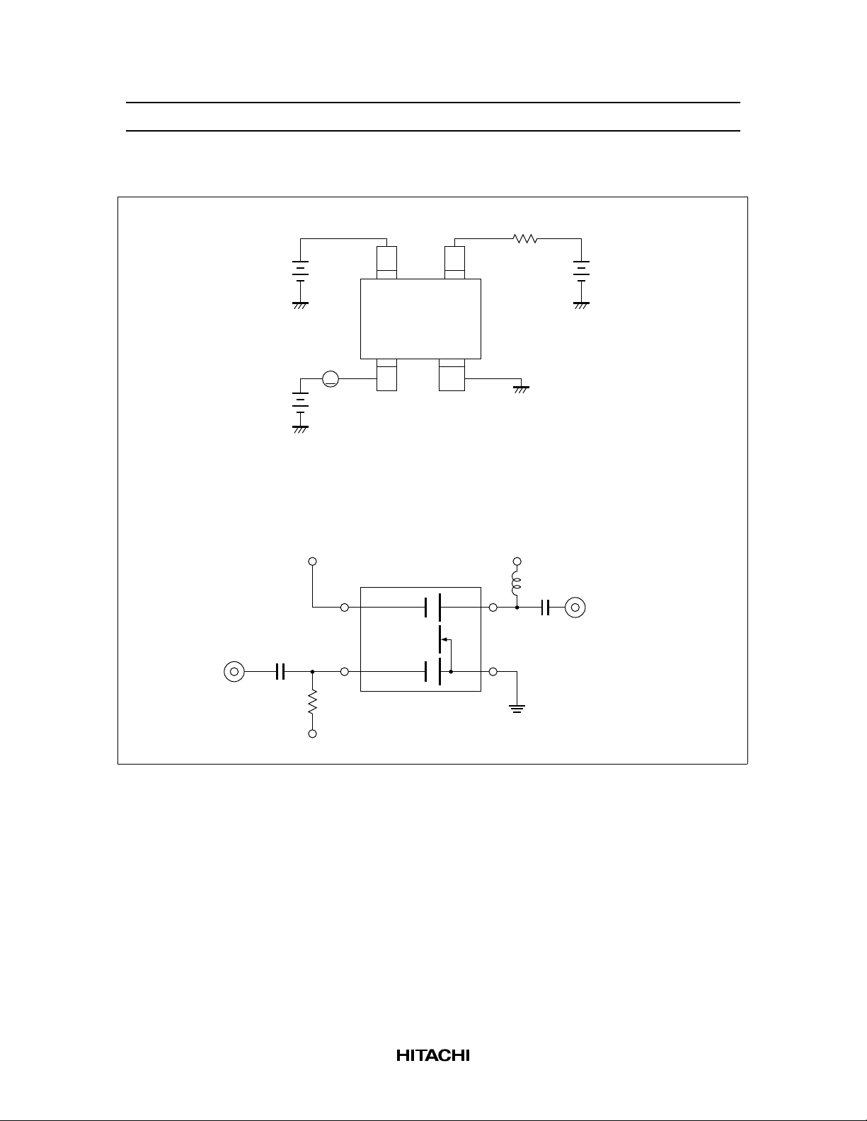
Test Circuit for Operating Items (I , |yfs|, Ciss, Coss, Crss, NF, PG)
V
G2 V
Gate 2
Drain
A
I
D
D(op)
Gate 1
Source
R
G
G1
Application Circuit
V = 4 to 0.3 V
AGC
BBFET
V = 5 V
DS
RFC
Output
Input
R
G
V = 5 V
GG
3
Page 4
BB601M
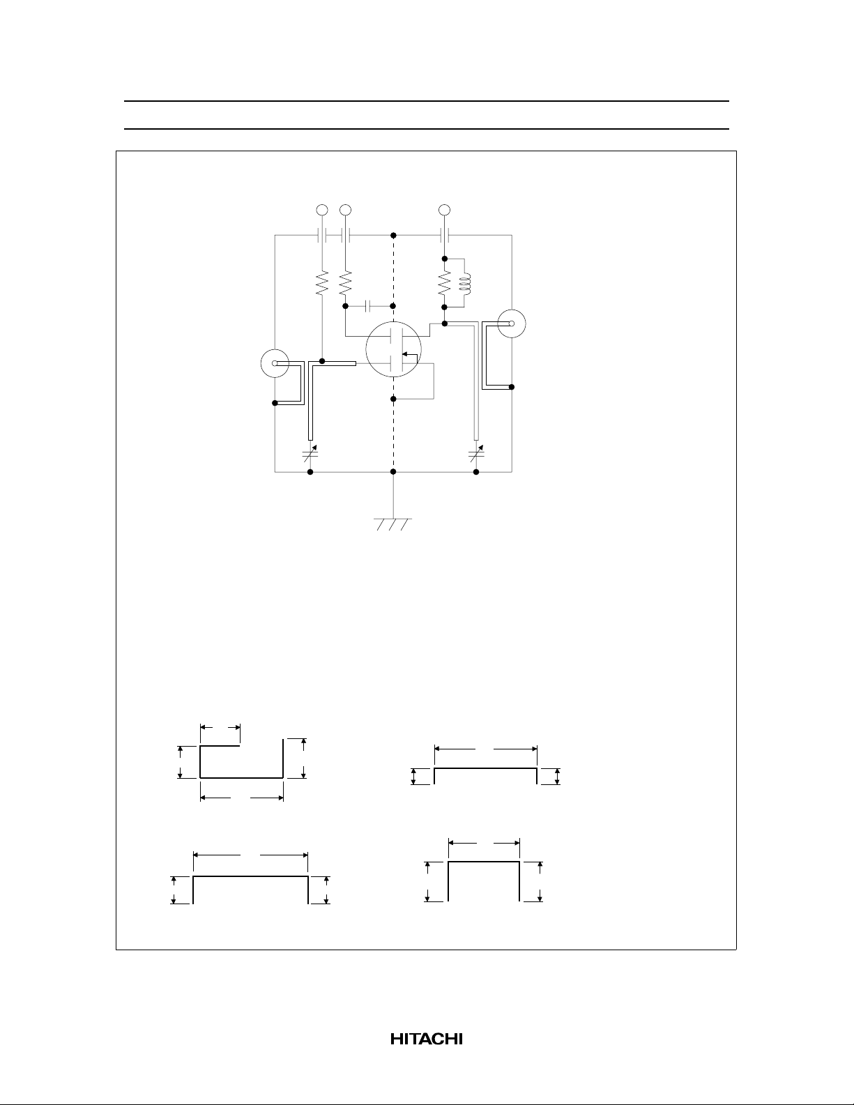
900MHz Power Gain, Noise Test Circuit
Input
V
G1
R1
L1
L2
C1, C2
C3
C4 — C6
R1
R2
R3
D
R3
S
V
D
C6
RFC
L3
V
G2
C5C4
R2
C3
G2
G1
:
Variable Capacitor (10pF MAX)
:
Disk Capacitor (1000pF)
:
Air Capacitor (1000pF)
:
47 kΩ
:
47 kΩ
:
4.7 kΩ
Output
L4
C2C1
L1:
L2:
10
26
8
10
3
(φ1mm Copper wire)
3
Unit: mm
21
L3:
L4:
29
7
7
10
18
10
RFC: φ1mm Copper wire with enamel 4turns inside dia 6mm
4
Page 5

BB601M
Maximum Channel Power
Dissipation Curve
200
150
100
50
Channel Power Dissipation Pch (mW)
0
50 100 150 200
Ambient Temperature Ta (°C)
20
Typical Output Characteristics
V = 4 V
G2S
V = V
G1 DS
16
D
12
8
Drain Current I (mA)
4
0
12345
Drain to Source Voltage V (V)
Ω
27 k
G
R = 22 k
33 k
100 k
DS
Ω
39 k
47 k
56 k
68 k
82 k
Ω
Ω
Ω
Ω
Ω
Ω
Ω
Drain Current vs. Gate1 Voltage
20
V = 5 V
DS
R = 33 kΩ
G
16
D
12
8
4
Drain Current I (mA)
0
12345
Gate1 Voltage V (V)
3 V
V = 1 V
G2S
G1
4 V
2 V
Drain Current vs. Gate1 Voltage
20
V = 5 V
DS
R = 47 kΩ
G
16
D
12
8
Drain Current I (mA)
4
0
12345
Gate1 Voltage V (V)
4 V
3 V
V = 1 V
G2S
G1
2 V
5
Page 6

BB601M
Drain Current vs. Gate1 Voltage
20
V = 5 V
DS
R = 68 kΩ
G
16
D
12
8
4
Drain Current I (mA)
0
12345
Gate1 Voltage V (V)
Forward Transfer Admittance
vs. Gate1 Voltage
30
V = 5 V
DS
R = 47 kΩ
24
G
f = 1 kHz
fs
18
4 V
2 V
3 V
V = 1 V
G2S
G1
4 V
3 V
2 V
Forward Transfer Admittance
vs. Gate1 Voltage
30
V = 5 V
DS
fs
24
R = 33 kΩ
G
f = 1 kHz
4 V
3 V
18
12
2 V
6
V = 1 V
Forward Transfer Admittance |y | (mS)
0
12345
Gate1 Voltage V (V)
G2S
G1
Forward Transfer Admittance
vs. Gate1 Voltage
30
V = 5 V
DS
R = 68 kΩ
fs
24
18
G
f = 1 kHz
4 V
2 V
3 V
12
6
Forward Transfer Admittance |y | (mS)
0
12345
Gate1 Voltage V (V)
6
V = 1 V
G2S
G1
12
6
V = 1 V
Forward Transfer Admittance |y | (mS)
0
12345
Gate1 Voltage V (V)
G2S
G1
Page 7
BB601M
Power Gain vs. Gate Resistance
30
25
20
15
V = V = 5 V
10
Power Gain PG (dB)
V = 4 V
f = 900 MHz
DS
G2S
G1
5
0
10
20 50
Gate Resistance R (k Ω )
Power Gain vs. Drain Current Noise Figure vs. Drain Current
30
G
100
Noise Figure vs. Gate Resistance
4
3
2
V = V = 5 V
V = 4 V
1
Noise Figure NF (dB)
0
10
f = 900 MHz
G1
DS
G2S
20 50
Gate Resistance R (k Ω )
4
100
G
25
20
15
V = V = 5 V
10
Power Gain PG (dB)
V = 4 V
R = variable
5
f = 900 MHz
0
0
G1
DS
G2S
G
5101520
Drain Current I (mA)
3
2
V = V = 5 V
1
Noise Figure NF (dB)
V = 4 V
R = variable
DS
G2S
G
G1
f = 900 MHz
0
0
D
5
Drain Current I (mA)
10
15 20
D
7
Page 8

BB601M
20
Drain Current vs. Gate Resistance
Power Gain vs.
Gate2 to Source Voltage
25
15
D
10
V = V = 5 V
5
0
10
V = 4 V
Drain Current I (mA)
G1
DS
G2S
20 50
Gate Resistance R (k Ω )
Noise Figure vs.
Gate2 to Source Voltage
5
4
G
V = 5 V
DS
R = 47 kΩ
G
f = 900 MHz
100
20
15
10
Power Gain PG (dB)
5
0
1
23
Gate2 to Source Voltage V (V)
Input Capacitance vs.
Gate2 to Source Voltage
4
3
V = 5 V
DS
R = 47 kΩ
G
f = 900 MHz
G2S
4
3
2
Noise Figure NF (dB)
1
1
Gate2 to Source Voltage V (V)
8
23
G2S
2
1
V = 5 V
DS
R = 47 kΩ
Input Capacitance Ciss (pF)
4
G
f = 1 MHz
0
0
1
Gate2 to Source Voltage V (V)
2
34
G2S
Page 9

Gain Reduction vs.
0
10
20
30
Gain Reduction GR (dB)
40
Gate2 to Source Voltage
V = V = 5 V
DS
V = 4 V
G2S
R = 47 kΩ
G
G1
BB601M
50
4
3
Gate2 to Source Voltage V (V)
2
10
G2S
9
Page 10

BB601M
S11 Parameter vs. Frequency
.8
.6
.4
.2
0
–.2
.2
–.4
Test Condition:
.6
.4
.8
–.6
–.8
V = 5 V , V = 5 V
DS
V = 4 V , R = 47 k ,
G2S
Zo = 50
50 — 1000 MHz (50 MHz step)
S12 Parameter vs. Frequency
120°
150°
180°
–150°
–120°
Test Condition:
50 — 1000 MHz (50 MHz step)
V = 5 V , V = 5 V
DS
V = 4 V , R = 47 k ,
G2S
Zo = 50
1
–1
90°
–90°
1.5
1.5
234
1
–1.5
G1
G
Ω
Scale: 0.002 / div.
G1
G
Ω
60°
–60°
S21 Parameter vs. Frequency
Scale: 1 / div.
90°
2
3
4
5
10
10
5
–10
–5
–4
–3
–2
150°
180°
–150°
Test Condition:
Ω
120°
–120°
–90°
V = 5 V , V = 5 V
DS
V = 4 V , R = 47 k ,
G2S
Zo = 50
Ω
G1
–60°
G
60°
30°
0°
–30°
Ω
50 — 1000 MHz (50 MHz step)
S22 Parameter vs. Frequency
1
.8
.6
.4
30°
0°
–30°
Ω
.2
0
–.2
.2
–.4
–.6
Test Condition:
.6
.4
.8
–.8
–1
V = 5 V , V = 5 V
DS
V = 4 V , R = 47 k ,
G2S
Zo = 50
50 — 1000 MHz (50 MHz step)
1.5
2
3
4
5
10
1.5
234
1
–1.5
G1
G
Ω
10
5
–10
–5
–4
–3
–2
Ω
10
Page 11

BB601M
Sparameter (VDS = VG1 = 5V, V
S11 S21 S12 S22
f (MHz) MAG ANG MAG ANG MAG ANG MAG ANG
50 0.974 –2.8 2.40 176.4 0.00057 78.1 0.997 –2.0
100 0.974 –10.0 2.38 172.2 0.00144 82.4 0.998 –4.2
150 0.974 –13.6 2.38 168.4 0.00211 78.7 0.997 –6.0
200 0.965 –16.5 2.37 164.1 0.00316 84.8 0.995 –8.1
250 0.963 –20.0 2.35 160.4 0.00358 76.3 0.994 –10.2
300 0.953 –23.7 2.32 156.8 0.00431 84.0 0.992 –12.2
350 0.947 –26.8 2.30 152.9 0.00503 79.0 0.990 –14.2
400 0.942 –29.6 2.28 148.6 0.00545 76.6 0.987 –16.2
450 0.929 –32.8 2.26 144.9 0.00630 80.3 0.984 –18.1
500 0.923 –35.4 2.21 141.2 0.00646 76.1 0.981 –20.2
550 0.912 –38.5 2.19 137.6 0.00693 73.7 0.977 –22.1
600 0.903 –41.2 2.15 134.2 0.00732 72.9 0.974 –24.1
650 0.886 –44.2 2.12 130.6 0.00729 74.6 0.971 –26.0
700 0.879 –46.8 2.08 127.4 0.00733 72.0 0.967 –27.8
750 0.873 –49.2 2.06 124.3 0.00762 74.5 0.962 –29.7
800 0.859 –52.4 2.03 120.8 0.00756 73.7 0.959 –31.7
850 0.846 –55.4 2.00 117.3 0.00772 75.5 0.955 –33.6
900 0.836 –58.0 1.96 114.3 0.00775 79.6 0.951 –35.5
950 0.827 –60.4 1.93 111.0 0.00801 81.7 0.946 –37.3
1000 0.815 –62.8 1.89 108.0 0.00704 81.0 0.942 –39.4
= 4V, RG = 47kΩ, Zo = 50Ω)
G2S
11
Page 12

BB601M
Package Dimensions
2.95
1.9
0.95 0.95
4
0.4
+ 0.1
– 0.05
±0.2
±0.2
Unit: mm
± 0.1
+ 0.1
0.4
– 0.05
0.65
3
0.16
+ 0.1
– 0.06
0.6
+ 0.1
– 0.05
± 0.2
± 0.15
2.8
1.5
1.8
2
0.95
0.4
+ 0.1
– 0.05
± 0.1
0.65
1
0.85
0—0.1
0.8
± 0.1
1.1
Hitachi Code
EIAJ
JEDEC
MPAK–4R
—
—
12
Page 13

Cautions
1. Hitachi neither warrants nor grants licenses of any rights of Hitachi’s or any third party’s patent,
copyright, trademark, or other intellectual property rights for information contained in this document.
Hitachi bears no responsibility for problems that may arise with third party’s rights, including
intellectual property rights, in connection with use of the information contained in this document.
2. Products and product specifications may be subject to change without notice. Confirm that you have
received the latest product standards or specifications before final design, purchase or use.
3. Hitachi makes every attempt to ensure that its products are of high quality and reliability. However,
contact Hitachi’s sales office before using the product in an application that demands especially high
quality and reliability or where its failure or malfunction may directly threaten human life or cause risk
of bodily injury, such as aerospace, aeronautics, nuclear power, combustion control, transportation,
traffic, safety equipment or medical equipment for life support.
4. Design your application so that the product is used within the ranges guaranteed by Hitachi particularly
for maximum rating, operating supply voltage range, heat radiation characteristics, installation
conditions and other characteristics. Hitachi bears no responsibility for failure or damage when used
beyond the guaranteed ranges. Even within the guaranteed ranges, consider normally foreseeable
failure rates or failure modes in semiconductor devices and employ systemic measures such as failsafes, so that the equipment incorporating Hitachi product does not cause bodily injury, fire or other
consequential damage due to operation of the Hitachi product.
5. This product is not designed to be radiation resistant.
6. No one is permitted to reproduce or duplicate, in any form, the whole or part of this document without
written approval from Hitachi.
7. Contact Hitachi’s sales office for any questions regarding this document or Hitachi semiconductor
products.
Hitachi, Ltd.
Semiconductor & Integrated Circuits.
Nippon Bldg., 2-6-2, Ohte-machi, Chiyoda-ku, Tokyo 100-0004, Japan
Tel: Tokyo (03) 3270-2111 Fax: (03) 3270-5109
URL NorthAmerica : http:semiconductor.hitachi.com/
For further information write to:
Hitachi Semiconductor
(America) Inc.
179 East Tasman Drive,
San Jose,CA 95134
Tel: <1> (408) 433-1990
Fax: <1>(408) 433-0223
Europe : http://www.hitachi-eu.com/hel/ecg
Asia (Singapore) : http://www.has.hitachi.com.sg/grp3/sicd/index.htm
Asia (Taiwan) : http://www.hitachi.com.tw/E/Product/SICD_Frame.htm
Asia (HongKong) : http://www.hitachi.com.hk/eng/bo/grp3/index.htm
Japan : http://www.hitachi.co.jp/Sicd/indx.htm
Hitachi Europe GmbH
Electronic components Group
Dornacher Stra§e 3
D-85622 Feldkirchen, Munich
Germany
Tel: <49> (89) 9 9180-0
Fax: <49> (89) 9 29 30 00
Hitachi Europe Ltd.
Electronic Components Group.
Whitebrook Park
Lower Cookham Road
Maidenhead
Berkshire SL6 8YA, United Kingdom
Tel: <44> (1628) 585000
Fax: <44> (1628) 778322
Hitachi Asia Pte. Ltd.
16 Collyer Quay #20-00
Hitachi Tower
Singapore 049318
Tel: 535-2100
Fax: 535-1533
Hitachi Asia Ltd.
Taipei Branch Office
3F, Hung Kuo Building. No.167,
Tun-Hwa North Road, Taipei (105)
Tel: <886> (2) 2718-3666
Fax: <886> (2) 2718-8180
Copyright ' Hitachi, Ltd., 1999. All rights reserved. Printed in Japan.
Hitachi Asia (Hong Kong) Ltd.
Group III (Electronic Components)
7/F., North Tower, World Finance Centre,
Harbour City, Canton Road, Tsim Sha Tsui,
Kowloon, Hong Kong
Tel: <852> (2) 735 9218
Fax: <852> (2) 730 0281
Telex: 40815 HITEC HX
 Loading...