

Page 1
查询BB403供应商
Features
• Build in Biasing Circuit; To reduce using parts cost & PC board space.
• High forward transfer admittance;
(|yfs| = 42 mS typ. at f = 1 kHz)
• Withstanding to ESD;
Build in ESD absorbing diode. Withstand up to 250V at C=200pF, Rs=0 conditions.
• Provide mini mold packages; MPAK-4R (SOT-143 var.)
BB403M
Build in Biasing Circuit MOS FET IC
VHF/UHF RF Amplifier
ADE-208-699A (Z)
2nd. Edition
Nov. 1998
Outline
Notes: 1. Marking is “CX–”.
2. BB403M is individual type number of HITACHI BBFET.
MPAK-4R
3
4
2
1
1. Source
2. Drain
3. Gate2
4. Gate1
Page 2

BB403M
Absolute Maximum Ratings (Ta = 25°C)
Item Symbol Ratings Unit
Drain to source voltage V
Gate1 to source voltage V
Gate2 to source voltage V
Drain current I
DS
G1S
G2S
D
Channel power dissipation Pch 150 mW
Channel temperature Tch 150 °C
Storage temperature Tstg –55 to +150 °C
Electrical Characteristics (Ta = 25°C)
Item Symbol Min Typ Max Unit Test Conditions
Drain to source breakdown voltage V
Gate1 to source breakdown
(BR)DSS
V
(BR)G1SS
voltage
Gate2 to source breakdown
V
(BR)G2SS
voltage
Gate1 to source cutoff current I
Gate2 to source cutoff current I
Gate1 to source cutoff voltage V
Gate2 to source cutoff voltage V
Drain current I
G1SS
G2SS
G1S(off)
G2S(off)
D(op)
Forward transfer admittance |yfs| 354250mSV
Input capacitance c
Output capacitance c
Reverse transfer capacitance c
iss
oss
rss
Power gain PG1 28 32 — dB VDS = 5V, VG1 = 5V
Noise figure NF1 — 1.0 1.6 dB f = 200MHz
Power gain PG2 12 16.5 — dB VDS = 5V, VG1 = 5V
Noise figure NF2 — 2.85 3.7 dB f = 900MHz
7 ——V I
+7——V I
+7——V I
— — +100 nA V
— — +100 nA V
0.3 0.6 0.9 V VDS = 5V, V
0.5 0.8 1.1 V VDS = 5V, V
9 1420mAV
2.6 3.3 4.0 pF VDS = 5V, VG1 = 5V
1.7 2.1 2.5 pF V
— 0.025 0.05 pF f = 1MHz
7V
– 0/ +7 V
– 0/ +7 V
25 mA
= 200µA
D
V
= V
G1S
= +10µA
G1
V
G2S
= +10µA
G2
V
G1S
G1S
V
G2S
G2S
V
G1S
I
= 100µA
D
I
= 100µA
D
DS
V
G2S
DS
V
G2S
R
= 470kΩ, f = 1kHz
G
G2S
V
G2S
V
G2S
= 0
G2S
= VDS = 0
= VDS = 0
= +5V
= VDS = 0
= +5V
= VDS = 0
= 4V
G2S
= 5V
G1S
= 5V, VG1 = 5V
= 4V, RG = 470kΩ
= 5V, VG1 = 5V
=4V
=4V, RG = 470kΩ
=4V, RG = 470kΩ
=4V, RG = 470kΩ
2
Page 3
Main Characteristics
BB403M
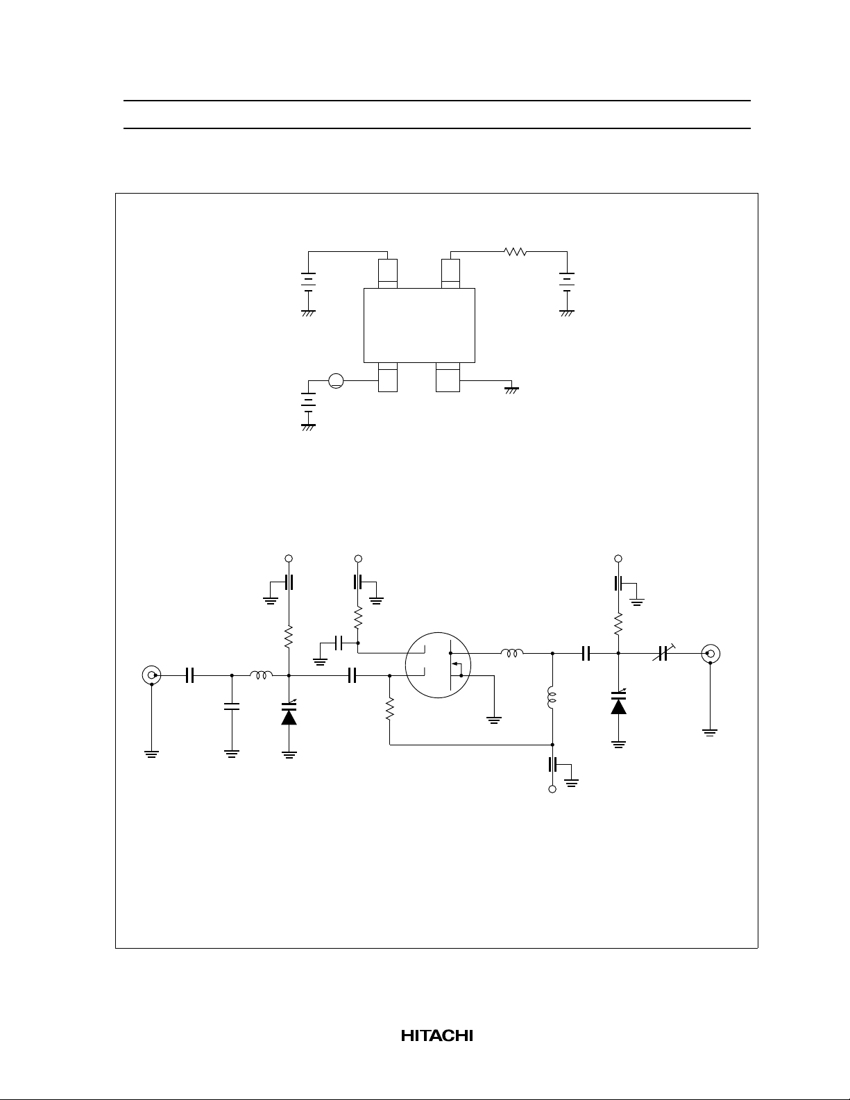
Test Circuit for Operating Items (I , |yfs|, Ciss, Coss, Crss, NF, PG)
V
G2
Gate 2
Drain
A
I
D
Power Gain, Noise Figure Test Circuit
V
G2
1000p
1000p
V
T
D(op)
Gate 1
Source
R
G
V
G1
V
T
1000p
Input(50Ω)
1000p
36p
BBFET
L2
470k
1000p
1000p
47k
R
G
1000p
47k
L1
1SV70
L1 : φ1mm Enameled Copper Wire,Inside dia 10mm, 2Turns
L2 : φ1mm Enameled Copper Wire,Inside dia 10mm, 2Turns
RFC : φ1mm Enameled Copper Wire,Inside dia 5mm, 2Turns
1000p
RFC
V = V
D G1
47k
10p max
1SV70
Unit Resistance (Ω)
Capacitance (F)
Output(50Ω)
3
Page 4
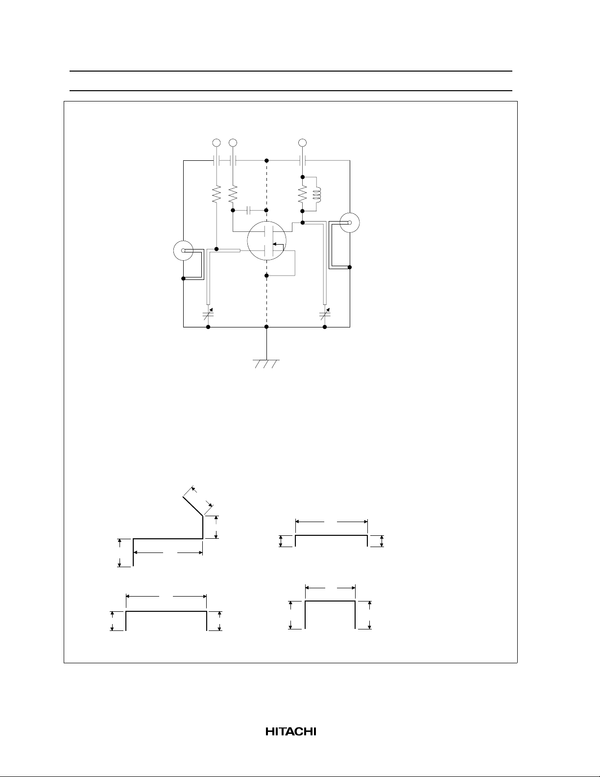
BB403M
900MHz Power Gain, Noise Test Circuit
Input
V
G1
R1
L1
L2
C1, C2
C4 to C6
V
G2
C5C4
R2
C3
G2
G1
:
Variable Capacitor (10pF MAX)
:
Disk Capacitor (1000pF)
C3
:
Air Capacitor (1000pF)
:
470 kΩ
R1
:
47 kΩ
R2
:
4.7 kΩ
R3
V
R3
D
S
D
C6
RFC
Output
L4
L3
C2C1
L1:
L2:
10
26
18
10
(φ1mm Copper wire)
3
Unit : mm
L3:
8
3
10
25
L4:
29
7
7
10
RFC : φ1mm Copper wire with enamel 4turns inside dia 6mm
4
Page 5
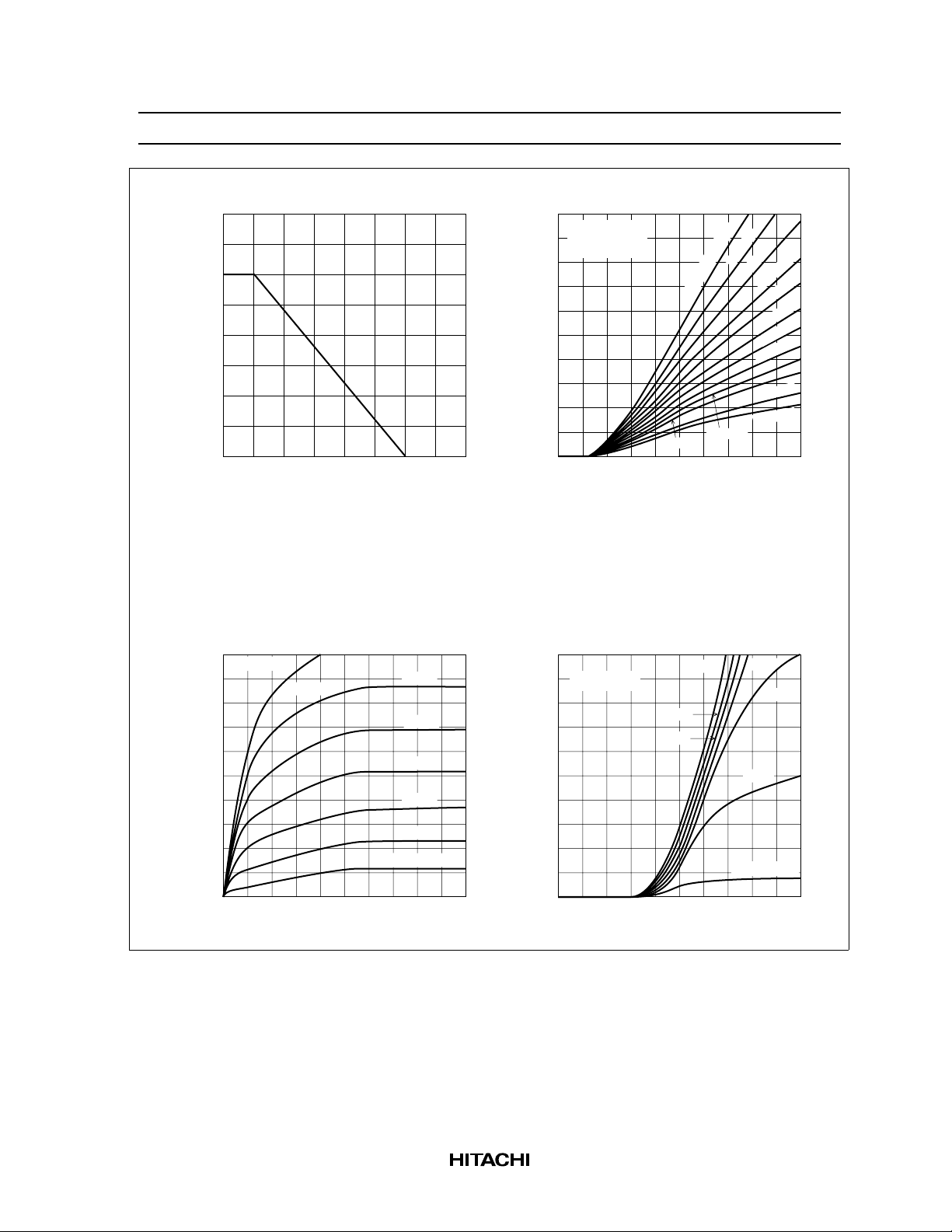
BB403M
Maximum Channel Power
Dissipation Curve
200
150
100
50
Channel Power Dissipation Pch (mW)
0
50 100 150 200
Ambient Temperature Ta (°C)
Drain Current vs.
25
Drain to Source Voltage
V = 4 V
G2S
1.5 V
1.4 V
20
1.3 V
D
15
1.2 V
10
1.1 V
25
Typical Output Characteristics
V = 4 V
G2S
V = V
G1 DS
20
D
15
10
Drain Current I (mA)
5
1 M
0
12345
Drain to Source Voltage V (V)
Drain Current vs.
Gate1 to Source Voltage
25
V = 5 V
DS
20
D
15
3.5 V
3 V
10
G
R = 180 k
820 k
Ω
4 V
Ω
220 k
Ω
Ω
270 k
680 k
1.5 M
2.2 M
DS
2.5 V
1.5 V
Ω
330 k
390 k
470 k
560 k
2 V
Ω
Ω
Ω
Ω
Ω
Ω
Ω
Drain Current I (mA)
5
0
12345
Drain to Source Voltage V (V)
1.0 V
V = 0.9 V
G1S
DS
5
Drain Current I (mA)
0
4.0 8.0 1.2 1.6 2.0
Gate1 to Source Voltage V (V)
V = 1 V
G2S
G1S
5
Page 6

BB403M
20
V = 5 V
DS
R = 470 k
G
16
D
12
8
Drain Current I (mA)
4
Drain Current vs.
Gate2 to Source Voltage
Ω
G1
V = 5 V
4.5 V
3.5 V
4 V
3 V
Drain Current vs. Gate1 Voltage
20
V = 5 V
DS
V = 4 V
G2S
16
D
12
R = 470 k
G
Ω
8
4
Drain Current I (mA)
0
12345
Gate2 to Source Voltage V (V)
Drain Current vs. Gate1 Current
25
20
D
15
10
Drain Current I (mA)
5
0
10 20 30 40 50
Gate1 Current I (µA)
G1
G2S
V = 5 V
DS
V = 4 V
G2S
Gate1 Current I (µA)
0
12345
Gate1 Voltage V (V)
Gate1 Current vs.
50
Gate1 to Source Voltage
V = 5 V
DS
40
G1
30
20
10
0
0.4 0.8 1.2 1.6 2.0
Gate1 to Source Voltage V (V)
G1
1.5 V
V = 1 V
G2S
G1S
4 V
2 V
3.5 V
3 V
2.5 V
6
Page 7

BB403M
Gate1 Current vs.
Gate2 to Source Voltage
10
V = 5 V
G1
8
6
DS
R = 470 k
G
Ω
4
2
Gate1 Current I (µA)
0
1.0 2.0 3.0 4.0 5.0
Gate2 to Source Voltage V (V)
Forward Transfer Admittance
vs. Gate1 Voltage
50
V = 5 V
fs
40
DS
R = 470 k
G
Ω
V = 5 V
G1
4.5 V
4 V
3.5 V
3 V
2.5 V
2 V
G2S
V = 4 V
G2S
Forward Transfer Admittance
50
fs
40
V = 5 V
DS
vs. Drain Current
3.5 V
4 V
2.5 V
30
20
10
Forward Transfer Admittance |y | (mS)
0
510152025
Drain Current I (mA)
V = 2 V
G2S
D
Power Gain vs. Gate Resistance
40
35
3 V
30
3 V
2 V
20
10
Forward Transfer Admittance |y | (mS)
0
12345
Gate1 Voltage V (V)
1 V
G1
30
25
20
V = 5 V
15
10
DS
V = 5 V
G1
V = 4 V
G2S
f = 200 MHz
Power Gain PG (dB)
0.1 0.2 0.5 1 2 5 10
Gate Resistance R (M )
G
Ω
7
Page 8

BB403M
Noise Figure vs. Gate Resistance
4
V = 5 V
DS
V = 5 V
G1
V = 4 V
3
G2S
f = 200 MHz
2
1
Noise Figure NF (dB)
0
0.1 0.2 0.5 1 2 5 10
Gate Resistance R (M W )
G
Noise Figure vs. Drain Current
4
V = 5 V
DS
V = 5 V
G1
V = 4 V
3
G2S
R = variable
G
f = 200 MHz
40
Power Gain vs. Drain Current
35
30
25
V = 5 V
20
Power Gain PG (dB)
15
10
DS
V = 5 V
G1
V = 4 V
G2S
R = variable
G
f = 200 MHz
0
510152025
Drain Current I (mA)
Power Gain vs. Gate Resistance
20
15
30
D
2
1
Noise Figure NF (dB)
0
8
510152025
Drain Current I (mA)
D
30
10
V = 5 V
5
Power Gain PG (dB)
DS
V = 5 V
G1
V = 4 V
G2S
f = 900 MHz
0
0.1 0.2 0.5 1 2 5 10
Gate Resistance R (M W )
G
Page 9

BB403M
Noise Figure vs. Gate Resistance
4
3
2
V = 5 V
1
Noise Figure NF (dB)
DS
V = 5 V
G1
V = 4 V
G2S
f = 900 MHz
0
0.1 0.2 0.5 1 2 5 10
Gate Resistance R (M W )
G
Noise Figure vs. Drain Current
4
3
20
Power Gain vs. Drain Current
15
10
5
Power Gain PG (dB)
0
510152025
Drain Current I (mA)
Gain Reduction vs.
Gate2 to Source Voltage
60
50
40
V = 5 V
DS
V = 5 V
G1
V = 4 V
G2S
R = variable
G
f = 900 MHz
D
V = V = 5 V
V = 4 V
R = 470 k
DS
G2S
G
G1
W
f = 200 MHz
30
2
1
Noise Figure NF (dB)
0
510152025
Drain Current I (mA)
V = 5 V
DS
V = 5 V
G1
V = 4 V
G2S
R = variable
G
f = 900 MHz
D
30
30
20
Gain Reduction GR (dB)
10
0
0123
Gate2 to Source Voltage V (V)
4
G2S
5
9
Page 10

BB403M
Gain Reduction vs.
Gate2 to Source Voltage
50
V = V = 5 V
DS
V = 4 V
40
G2S
R = 470 k
G
f = 900 MHz
30
20
Gain Reduction GR (dB)
10
0
12345
Gate2 to Source Voltage V (V)
Input Capacitance vs.
Gate2 to Source Voltage
4
G1
W
G2S
Drain Current vs. Gate Resistance
35
V = 5 V
30
DS
V = 5 V
G1
V = 4 V
G2S
25
D
20
15
10
Drain Current I (mA)
5
0
0.1 0.2 0.5 1 2 5 10
Gate Resistance R (M )
G
W
3
2
1
Input Capacitance Ciss (pF)
0
1234
Gate2 to Source Voltage V (V)
V = 5 V
DS
V = 5 V
G1
V = 4 V
G2S
R = 470 k
G
f = 1 MHz
G2S
W
10
Page 11

BB403M
S11 Parameter vs. Frequency
1
.6
.4
.2
0
–.2
.2
–.4
–.6
Test Condition :
.8
.6
.4
.8
–.8
–1
V = 5 V , V = 5 V
DS
V = 4 V , R = 470 k
G2S
Zo =50
1.5
2
3
4
5
10
1.5
234
1
–1.5
G1
G
Ω
10
5
–10
–5
–4
–3
–2
Ω
50 to 1000 MHz (50 MHz step)
S12 Parameter vs. Frequency
Scale: 0.002 / div.
90°
120°
150°
180°
–150°
–120°
Test Condition : Test Condition :
–90°
V = 5 V , V = 5 V
DS
V = 4 V , R = 470 k
G2S
Ω
Zo =50
50 to 1000 MHz (50 MHz step)
G1
G
60°
30°
0°
–30°
–60°
Ω
S21 Parameter vs. Frequency
150°
180°
–150°
–120°
Test Condition :
50 to 1000 MHz (50 MHz step)
S22 Parameter vs. Frequency
.4
.2
0
–.2
–.4
50 to 1000 MHz (50 MHz step)
90°
120°
–90°
V = 5 V , V = 5 V
DS
V = 4 V , R = 470 k
G2S
Ω
Zo =50
1
.8
.6
.2
.6
.4
–.6
1
.8
–.8
–1
V = 5 V , V = 5 V
DS
V = 4 V , R = 470 k
G2S
Ω
Zo =50
Scale: 1 / div.
60°
–60°
G1
G
1.5
1.5
234
–1.5
G1
G
30°
0°
–30°
Ω
2
3
4
5
10
10
5
–10
–5
–4
–3
–2
Ω
11
Page 12

BB403M
Sparameter (VDS = VG1 = 5V, V
S11 S21 S12 S22
f (MHz) MAG ANG MAG ANG MAG ANG MAG ANG
50 0.947 –7.0 4.11 174.4 0.00400 89.0 0.985 –3.1
100 0.978 –11.9 4.13 167.1 0.00305 116.5 0.985 –6.8
150 0.973 –18.7 4.04 159.8 0.00266 75.5 0.982 –10.1
200 0.960 –23.8 4.01 152.7 0.00384 66.8 0.978 –13.5
250 0.956 –29.6 3.90 146.4 0.00453 70.1 0.970 –16.8
300 0.939 –35.5 3.85 139.9 0.00440 59.6 0.965 –20.0
350 0.930 –40.3 3.68 133.6 0.00550 67.2 0.957 –23.1
400 0.905 –45.7 3.63 128.3 0.00571 59.0 0.949 –26.2
450 0.889 –50.3 3.45 122.7 0.00583 54.2 0.940 –29.2
500 0.870 –55.6 3.35 116.6 0.00634 51.6 0.932 –32.1
550 0.855 –59.6 3.22 111.5 0.00596 56.2 0.924 –35.0
600 0.841 –63.9 3.10 106.3 0.00591 55.7 0.917 –37.7
650 0.826 –67.9 3.02 101.4 0.00544 54.9 0.908 –40.5
700 0.812 –71.8 2.89 96.1 0.00533 57.2 0.900 –43.1
750 0.799 –75.6 2.78 91.8 0.00495 64.6 0.893 –45.7
800 0.788 –78.9 2.70 87.5 0.00470 66.5 0.887 –48.1
850 0.778 –82.6 2.60 82.2 0.00460 75.1 0.880 –50.6
900 0.765 –85.8 2.48 78.1 0.00445 83.8 0.874 –52.9
950 0.763 –88.8 2.41 74.2 0.00486 97.0 0.869 –55.3
1000 0.748 –92.2 2.34 69.7 0.00502 102.6 0.864 –57.5
= 4V, RG = 470kΩ, Zo = 50Ω)
G2S
12
Page 13

Package Dimensions
2.95
0.95 0.95
4
0.4
+ 0.1
– 0.05
1.9
±0.2
±0.2
BB403M
Unit: mm
± 0.1
+ 0.1
0.4
– 0.05
0.65
3
0.16
+ 0.1
– 0.06
0.6
+ 0.1
– 0.05
± 0.2
± 0.15
2.8
1.5
1.8
2
0.95
0.4
+ 0.1
– 0.05
± 0.1
0.65
1
0.85
0 ~ 0.1
0.8
± 0.1
1.1
Hitachi Code
EIAJ
JEDEC
MPAK–4R
—
—
13
Page 14

BB403M
Cautions
1. Hitachi neither warrants nor grants licenses of any rights of Hitachi’s or any third party’s patent, copyright,
trademark, or other intellectual property rights for information contained in this document. Hitachi bears no
responsibility for problems that may arise with third party’s rights, including intellectual property rights, in
connection with use of the information contained in this document.
2. Products and product specifications may be subject to change without notice. Confirm that you have
received the latest product standards or specifications before final design, purchase or use.
3. Hitachi makes every attempt to ensure that its products are of high quality and reliability. However, contact
Hitachi’s sales office before using the product in an application that demands especially high quality and
reliability or where its failure or malfunction may directly threaten human life or cause risk of bodily injury,
such as aerospace, aeronautics, nuclear power, combustion control, transportation, traffic, safety equipment
or medical equipment for life support.
4. Design your application so that the product is used within the ranges guaranteed by Hitachi particularly for
maximum rating, operating supply voltage range, heat radiation characteristics, installation conditions and
other characteristics. Hitachi bears no responsibility for failure or damage when used beyond the guaranteed
ranges. Even within the guaranteed ranges, consider normally foreseeable failure rates or failure modes in
semiconductor devices and employ systemic measures such as fail-safes, so that the equipment incorporating
Hitachi product does not cause bodily injury, fire or other consequential damage due to operation of the
Hitachi product.
5. This product is not designed to be radiation resistant.
6. No one is permitted to reproduce or duplicate, in any form, the whole or part of this document without
written approval from Hitachi.
7. Contact Hitachi’s sales office for any questions regarding this document or Hitachi semiconductor products.
Hitachi, Ltd.
Semiconductor & IC Div.
Nippon Bldg., 2-6-2, Ohte-machi, Chiyoda-ku, Tokyo 100-0004, Japan
Tel: Tokyo (03) 3270-2111 Fax: (03) 3270-5109
URL NorthAmerica : http:semiconductor.hitachi.com/
For further information write to:
Hitachi Semiconductor
(America) Inc.
2000 Sierra Point Parkway
Brisbane, CA 94005-1897
Tel: <1> (800) 285-1601
Fax: <1> (303) 297-0447
Europe : http://www.hitachi-eu.com/hel/ecg
Asia (Singapore) : http://www.has.hitachi.com.sg/grp3/sicd/index.htm
Asia (Taiwan) : http://www.hitachi.com.tw/E/Product/SICD_Frame.htm
Asia (HongKong) : http://www.hitachi.com.hk/eng/bo/grp3/index.htm
Japan : http://www.hitachi.co.jp/Sicd/indx.htm
Hitachi Europe GmbH
Electronic components Group
Dornacher Straße 3
D-85622 Feldkirchen, Munich
Germany
Tel: <49> (89) 9 9180-0
Fax: <49> (89) 9 29 30 00
Hitachi Europe Ltd.
Electronic Components Group.
Whitebrook Park
Lower Cookham Road
Maidenhead
Berkshire SL6 8YA, United Kingdom
Tel: <44> (1628) 585000
Fax: <44> (1628) 778322
14
Hitachi Asia Pte. Ltd.
16 Collyer Quay #20-00
Hitachi Tower
Singapore 049318
Tel: 535-2100
Fax: 535-1533
Hitachi Asia Ltd.
Taipei Branch Office
3F, Hung Kuo Building. No.167,
Tun-Hwa North Road, Taipei (105)
Tel: <886> (2) 2718-3666
Fax: <886> (2) 2718-8180
Copyright © Hitachi, Ltd., 1998. All rights reserved. Printed in Japan.
Hitachi Asia (Hong Kong) Ltd.
Group III (Electronic Components)
7/F., North Tower, World Finance Centre,
Harbour City, Canton Road, Tsim Sha Tsui,
Kowloon, Hong Kong
Tel: <852> (2) 735 9218
Fax: <852> (2) 730 0281
Telex: 40815 HITEC HX
 Loading...