

HITACHI 53UWX10B, 61UWX10B, 53UDX10B, 61UDX10B, 43FDX10B Training Manual
...
MARCH 2006 Training Materials Prepared by: ALVIE RODGERS C.E.T.
2001
MODEL RELEASE
DIGITAL
HD READY PTV
Chassis Model # Aspect
DP-14G 43UWX10B 16X9
53UWX10B
61UWX10B
DP-15 53UDX10B 4X3
61UDX10B
DP-15E 43FDX10B 4X3
43FDX11B
DP-17 53SWX10B 16X9
61SWX10B
53SWX12B Regional
61SWX12B Regional
Anti-Glare
Ultra Shield Included
CONTENTS... 2002 DP-1X Chassis Projection Television Information
INSTRUCTOR… Alvie Rodgers C.E.T. (Chamblee, GA.)

THIS PAGE INTENTIONALLY LEFT BLANK

MARCH 2006
SECTION (1) MICROPROCESSOR INFORMATION:
DP-1X CHASSIS Table of Contents Page 1 of 3
• Microprocessor DATA COMMUNICATION Explanation -------------- ----------------------- 01-01
• Microprocessor with SRS DATA COMMUNICATION Circuit Diagram -------------------- 01-05
• Microprocessor with DSP DATA COMMUNICATION Circuit Diagram -------------------- 01-06
• DAC 1 and DAC 3 (I006 & I007) Pin Function Explanation ----------------------------------- 01-07
• On Screen Display OSD Signal Path Explanation ------------------------------------------------- 01-08
• On Screen Display OSD Signal Path Circuit Diagram ------------------------------------------ --- 01-10
• Audio and Video MUTE Explanation ------ -------------------------------- ------------------------- 01-11
• Audio and Video MUTE SRS Circuit Diagram ---------------------------------------------------- 01-13
• Audio and Video MUTE DSP Circuit Diagram ---------------------------------------------------- 01-14
• SRS PWB MUTE Circuit Diagram ------------------------------------------------------------------ 01-15
• DP-17 SURROUND PWB MUTE Circuit Diagram --------------------------------------------- 01-16
• MEMORY INITIALIZATION Explanation ------------------------------------------------------ 01-17
• FACTORY RESET CONDITIONS (Shipping Condition) ------------------------------------- 01-18
• EEPROM I
SECTION (2) POWER SUPPLY DIAGRAMS:
2
C Average Data Values --------- ------------------------- ------------------------- ----- 01-20
• POWER ON /OF F Explanation ---------------------------------------------------------------------- 02-01
• POWER ON/OFF DP-14G and DP-17 Circuit Diagram ---------------------------------------- 02-04
• POWER ON/OFF DP-15 Circuit Diagram ----------- ----- ---- --- ---- ----- ---- ----- -- ---- ----- ---- - 02-05
• Sub Power Supply Distrib ution and Protection Block Diagram --------------------------------- 02-06
• Low Voltage Power Supply SHUT DOWN Explanation ----------------------------------------- 02-07
• Low Voltage Power Supply SHUT DOWN Diagram --------------------------------------------- 02-10
• Green LED Used in Low Vol tage Power Suppl y for Visual Trouble Shoo ting Explanation 02-11
• Green LED Used in Low Voltage Power Supply for Visual Trouble Shooting ---------------- 02-12
• DP-17 Green LEDs Used in Low Voltage Power Supply Explanation ------------------------- 02-13
• DP-17 Green LEDs Used in Low Voltage Power Supply for Visual Trouble Shooting ------ 02-14
• Deflection Power Supply Distribution and Protection Block Diagram ------------------------- 02-15
• High Voltage Power Supply SHUT DOWN Explanation ---------------------------------------- 02-16
• High Voltage Power Supply SHUT DOWN Diagram -------------------------------------------- 02-21
• High Voltage Green and Red LED Used for Visual Trouble Shooting Explanation ---------- 02-22
• High Voltage Green and Red LED Used for Visual Trouble Shooting ------------------------- 02-24
SECTION (3) DEFLECTION CIRCUIT:
• DEFLECTION BLOCK DIAGRAM Circuit Description -------------------------------------- 03-01
• DEFLECTION BLOCK DIAGRAM Circuit ---------------------------------------------------- 03-04
• HORIZONTAL DRIVE Circuit Description (Updated 04-2006) ------------------------------- 03-05
• HORIZONTAL DRIVE Circuit Diagram --------------------------------------------------------- 03-07
• HORIZONTAL DRIVE IC Voltages and Waveform Information --------------------------- 03-08
• Horizontal and Vertical SWEEP LOSS Detection Circuit Description ------------------------ 03-09
• Horizontal and Vertical SWEEP LOSS Detection Circuit ------------------------------------ --- 03-10
• Vertical SQUEEZE Display Diagra ms -------------------------------------------------------------- 03-11
• Vertical SQUEEZE Circuit Diagram ---------------------------------------------------------------- 03-12
• VERTICAL OUTPUT with V. SQUEEZE Circuit ---------------------------------------------- 03-13
• DP-17 VERTICAL OUTPUT without V. SQUEE ZE Circuit --------------------------------- 03-14
• SIDE PIN CUSHION Circuit Diagra m ------------------------------------------------------------- 03-15
Continued on Next Page

MARCH 2006 DP-1X CHASSIS Table of Contents Page 2 of 3
Continued from Previous Page
SECTION (4) DIGITAL CONVERGENCE CIRCUIT INFORMATION:
• DIGITAL CONVERGENCE Interface Circuit Description ------------------------------------- 04-01
• DIGITAL CONVERGENCE Interface Circuit Diagram ---------------------------------------- 04-05
• REMOTE CONTROL CLU-5711 in DIGI TAL CONVERGENCE MODE ----------------- 04-06
• REMOTE CONTROL CLU-5712 in DIGI TAL CONVERGENCE MODE ----------------- 04-07
• REMOTE CONTROL CLU-4311 in DIGI TAL CONVERGENCE MODE ----------------- 04-08
• OVERLAY DIMENSIONS for 43” (4X3 Aspect) Models -------------------------------------- 04-09
• OVERLAY DIMENSIONS for 53” (4X3 Aspect) Model --------------------------------------- 04-10
• OVERLAY DIMENSIONS for 61” (4X3 Aspect) Model --------------------------------------- 04-11
• OVERLAY DIMENSIONS for 43” & 53” (16X9 Aspect) Model ------------------------------ 04-12
• OVERLAY DIMENSIONS for 61” (16X9 Aspect) Model ------------------- ------------------- 04-13
• OVERLAY Part Numbers ---------------------------------------------------------------------------- 04-14
SECTION (5) VIDEO CIRCUIT INFORMATION:
• VIDEO Signal NTSC Circuit Diagram (1 of 2) -------------------------------------------------- 05-01
• VIDEO Signal NTSC, COMPONENT, and OSD Circuit Diagram (2 of 2) ---------------- 05-02
• IC-01 Pin 17, 24 and 52 Signal Description ------------------------------------------------------ 05-03
• Auto Brightness Limiter ABL Description ------------------------------------------------------ 05-04
• Auto Brightness Limiter ABL Circuit ------------------------------------------------------------- 05-05
• NTSC SYNC Circuit Diagram ---------------------------------------------------------------------- 05-06
• COMPONENT SYNC SEPARATION Circuit Diagram -------------------------------------- 05-07
SECTION (6) ADJUSTMENT INFORMATION:
• ADJUSTMENT ORDER ---------------------------------------------------------------------------- 06-01
• PRE HEAT RUN -------------------------------------------------------------------------------------- 06-02
• CUT OFF ADJUSTMENT -------------------------------------------------------------------------- 06-03
• PRE-FOCUS ADJUSTMENT ---------------------------------------------------------------------- 06-04
• DCU CROSS HATCH PHASE SETTING ------------------------------------------------------- 06-05
• HORIZONTAL POSITION (COARSE) ADJUSTMENT ------------------------------------ 06-06
• RASTER TILT ADJUSTMENT ------------------------------------------------------------------- 06-07
• BEAM ALIGNMENT ADJUSTMENT ----------------------------------------------------------- 06-08
• RASTER POSITION [Off-Set for Red and Blue] ADJUSTMENT ------------------------- 06-09
• VERTICAL SIZE ADJUSTMENT ---------------------------------------------------------------- 06-10
• HORIZONTAL SIZE ADJUSTMENT ----------------------------------------------------------- 06-11
• BEAM FORM ADJUSTMENT -------------------------------------------------------------------- 06-12
• LENS FOCUS ADJUSTMENT --------------------------------------------------------------------- 06-13
• STATIC FOCUS ADJUSTMENT ----------------------------------------------------------------- 06-14
• BLUE DE-FOCUS ADJUSTMENT --------------------------------------------------------------- 06-15
• WHITE BALANCE and SUB BRIGHTNESS ADJUSTMENT ----------------------------- 06-16
• HORIZONTAL POSITION (FINE) ADJUSTMENT ------------------------------------------ 06-17
• HD FOCUS CHARACTER SET UP ADJUSTMENT ----------------------------------------- 06-18
• HD FOCUS PATTERN SET UP ADJUSTMENT ---------------------------------------------- 06-19
Continued on Next Page

MARCH 2006
Continued from Previous Page
SECTION (6) ADJUSTMENT INFORMATION (Continued):
DP-1X CHASSIS Table of Contents Page 3 of 3
• DIGITAL CONVERGENCE ALIGNMENT PROCEDURE -------------------------------- 06-20
• STORING DIGITAL CONVERGENCE DATA ----------------------------------------------- 06-28
• INITIALIZING HD FOCUS SENSORS --------------------------------------------------------- 06-29
• CONVERGENCE TOUCH UP --------------------------------------------------------------------- 06-30
• REMOTE CONTROL CLU-5711 in DIGI TAL CONVERGENCE MODE ----------------- 06-31
• REMOTE CONTROL CLU-5712 in DIGI TAL CONVERGENCE MODE ----------------- 06-32
• REMOTE CONTROL CLU-4311 in DIGI TAL CONVERGENCE MODE ----------------- 06-33
• MAGNET LOCATIONS ---------------------------------------------------------------------------- 06-34
• SUB PICTURE (PIP) AMPLITUDE ADJUSTMENT ----------------------------------------- 06-35
• ERROR CODES for DCU HD FOCUS Description -------------------------------------------- 06-36
SECTION (7) AUDIO CIRCUIT INFORMATION:
• AUDIO SIGNAL (Main & Terminal) Circuit Diagram --------------------------------------- 07-01
• AUDIO SRS Circuit Diagram ---------------------------------------------------------------------- 07-02
• DP-17 AUDIO SIGNAL (Main & Terminal) Circuit Diagram ------------------------------ 07-03
• DP-17 AUDIO SURROUND Circuit Diagram -------------------------------------------------- 07-04
SECTION (8) MISCELLANEOUS INFORMATION:
• DP-1X (Not DP-17) REAR PANEL ---------------------------------------------------------------- 08-01
• DP-17 REAR PANEL --------------------------------------------------------------------------------- 08-02
• DEFLECTION / POWER PWB -------------------------------------------------------------------- 08-03
• SUB POWER SUPPLY PWB ----------------------------------------------------------------------- 08-04
• SIGNAL PWB ------------------------------------------------------------------------------------------ 08-05
• CRT PWB ----------------------------------------------------------------------------------------------- 08-06
• CONVERGENCE PWB ----------------------------------------------------------------------------- 08-07
• TERMINAL PWB ------------------------------------------------------------------------------------- 08-08
• SRS (SURROUND) PWB ---------------------------------------------------------------------------- 08-09
• CHASSIS TOTAL ------------------------------------------------------------------------------------- 08-10
• DC VOLTAGES --------------------------------------------------------------------------------------- 08-11
• OVERLAY PART NUMBERS --------------------------------------------------------------------- 08-20
SECTION (9) SERVICE BULLETINS AND INFORMATION:
• PTV 01-01 Clarification of Memory Initialization Procedure ------------------------------------ 09-01
• PTV 01-02 Horizontal Noise Present when Cold (Anode Cup Arc) ---------------------------- 09-03
• PTV 01-04 Excessive Noise in PinP ----------------------------------------------------------------- 09-04
• PTV 01-05 Digit al Convergence Adjustment Mode Ac cess via Remote Control ------------- 09-05
• PTV 01-06 Intermittent Black Horizontal Bars (Low AC) --------------------------------------- 09-06
• PTV 01-08A Glue Residue when Removing Protective Plastic Sheet from Screen ----------- 09-07
• PTV 01-10 STOP displayed (CRT Snap) ----------------------------------------------------------- 09-08
• PTV 01-14 Symmetry (Geometry) Adjustments --------------------------------------------------- 09-10
• Poor Picture Qualit y when watching NTSC on a 2H (HD Ready) set ---------------------- 09-11
• Things Yo u Shou ld Know: Rand om Shutdown, Re lay Stick, Coil Backwards, etc... ------- 09-12

THIS PAGE INTENTIONALLY LEFT BLANK

MICROPROCESSOR
INFORMATION
DP-1X CHASSIS
SECTION 1

THIS PAGE INTENTIONALLY LEFT BLANK
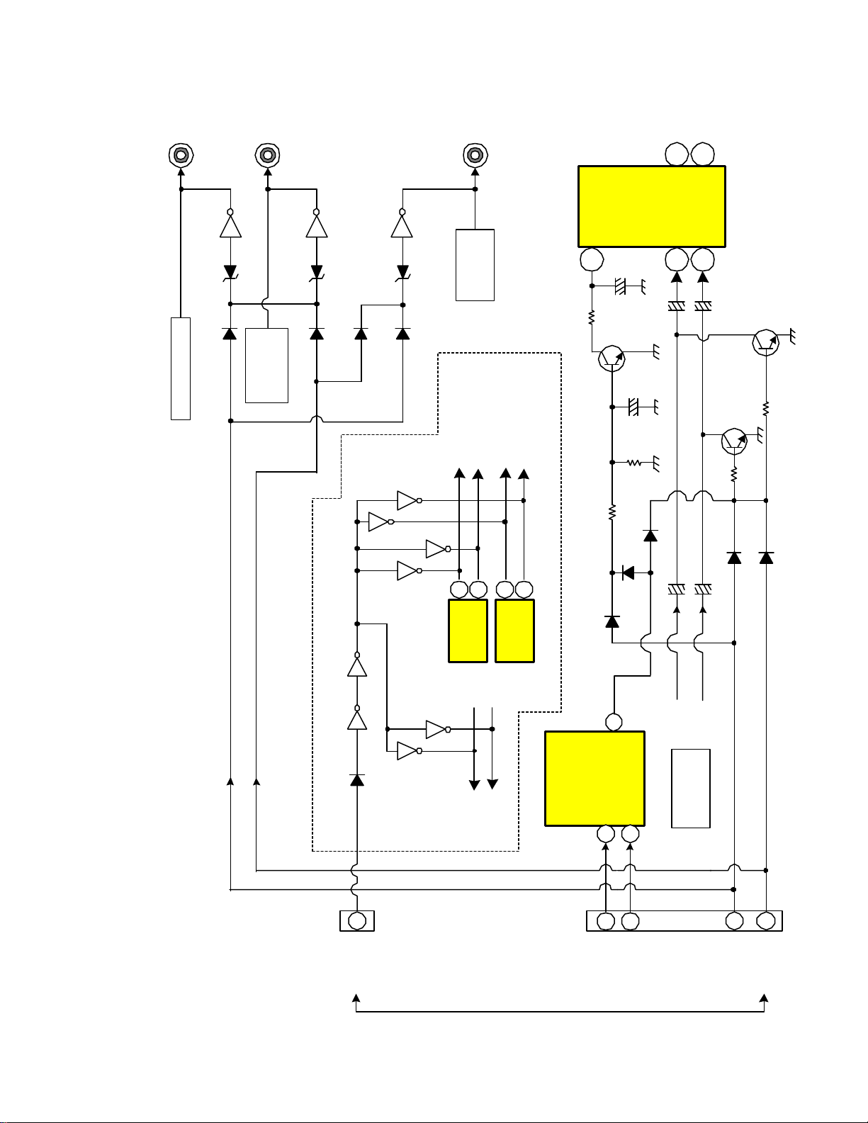
DP-1X MICROPROCESSOR DATA COMMUNICATION DESCRIPTION
Microprocessor Data Communications circuit diagram. (See Diagram on page 01-06)
The Microprocessor must keep in communication with the Chassis to maintain control over the individual circuits. Some of the circuits must return information as well so the Microprocessor will know how to respond to
different request.
The Microprocessor uses a combination of I
control. The I
2
C communication scheme only requires 2 lines for control. These lines are called SDA and SCL.
Serial Data and Serial Clock respectively.
The Microprocessor also requires the use of what are called Fan Out IC or DACs, (Digital to Analog Converters).
This allows the Microprocessor to use only two lines to control many different circuits.
Also, due to the fact that this Microprocessor operates at the new 3.3Vdc voltage, it requires a Level Shift IC to
bring up the DC level of the control lines to make it compatible with the connected ICs.
The Microprocessor communicates with the following ICs:
ON THE SIGNAL PWB:
Main Tuner U501
PinP Tuner U502
EEPROM I002
Flex Converter UC01
DAC1 I006
DAC3 I007
Level Shift I004
3D Y/C I301
Main Video Chroma I501
Rainforest IC01
ON THE TERMINAL PWB:
A/V Selector IX01
Sub Video Chroma IX03
Main Y Pr/Pb Selector IX04
Sub Y Pr/Pb Selector IX05
ON THE SURROUND PWB:
Front Audio Control IA01
The following explanation will deal with the communication paths used between the Microprocessor and the respected ICs.
ON THE SIGNAL PWB:
Main Tuner U501 (with MTS outputs).
The Microprocessor controls the Main Tuner by SDA (Data) and SCL (Clock) I
SCL1 and SDA1 lines for the Main Tuner are output from the Microprocessor at pins (
spectively. These lines go directly to the Main Tuner, SDA1 at pin (5) and SCL1 at pin (4). These lines control
band switching, programmable divider set-up information, pulse swallow tuning selection, etc...
PinP Tuner U502 (monaural only, but audio not used).
The Microprocessor controls the Main Tuner by SDA (Data) and SCL (Clock) I
SCL1 and SDA1 lines for the Main Tuner are output from the Microprocessor at pins (
spectively. These lines go directly to the Main Tuner, SDA1 at pin (5) and SCL1 at pin (4). These lines control
band switching, programmable divider set-up information, pulse swallow tuning selection, etc...
EEPROM I003
The EEPROM is ROM for many different functions of the Microprocessor. Channel Scan or Memory List, Customer set ups for Video, Audio, Surround etc… are memorized as well. Also, some of the Microprocessors internal sub routines have variables that are stored in the EEPROM, such as the window for Closed Caption detection.
2
C Bus communication and the Serial Data, Clock and Load lines for
2
C communication lines.
2 SDA1 and 3 SCL1
2
C communication lines.
2 SDA1 and 3 SCL1
(Continued on page 2)
) re-
) re-
PAGE 01-01
DP-1X MICROPROCESSOR DATA COMMUNICATION DESCRIPTION
(Continued from page 1)
Data and Clock lines are SDA1 from pin (2) of the Microprocessor to pin (5) of the EEPROM and SCL2 from
pin (3) of the Microprocessor to pin (6) of the EEPROM. Data travels in both directions on the Data line.
Flex Converter UC01
The projection television is capable of displaying NTSC as well as ATSC (DTV) including HD (High Definition). The Flex Converter is responsible for receiving any video input and converting it to 33.75 Khz output.
This output is controlled by sync and by the customer’s menu and how it is set up. The set up can be 4X3 or
16X9 for DTV, or letterbox. This set also has something called “Through Mode”. This bypasses the Flex Converter completely and inputs the 1080i signal directly to the Rainforest IC. The Rainforest IC then output the
signal directly as well as shrinking the vertical to match the 16 X 9 window by outputting “Vertical Squeeze”,
(V Squeeze not used for the 16 X 9 models). The Flex Converter can take any NTSC, S-In, Component, NTSC
or Progressive, Interlaced, 480I, 720P, 1080i signal. (Note: 1080i is routed through the Rainforest IC in 16 X 9
HD mode only).
Control for the Flex Converter is Clock, Data and Enable lines.
Clock, Data and Enable lines for the Flex Converter are output from the Microprocessor at pins (45 Data and
46 FCENABLE). The FCENABLE line is routed through the PFC1 connector pin 12 and the FCDATA line is
routed through the PFC1 connector pin 11.
The Clock line must be routed through the Level Shift IC I004 to be brought up to 5V. The Microprocessor
output for Clock is pin 58, it arrives at I004 at pins (3 Clock) and is output at pins (17). It arrives at the Flex
Converter through the PFC1 connector pin 10.
DAC1 I006 (See Diagram on page 01-07)
This Digital to Analog converter acts as an extension of the Microprocessor. Sometimes called an Expansion
IC. The purpose of this IC is to reduce the number of pins, (fan out) of the Main Microprocessor I001. The
Main Microprocessor send Clock and Data via I2C bus to the DAC1 IC. The output from the Microprocessor is
pin (2 SDA1 and 3 SCL1) which arrives at the DAC1 IC I006 at pins (5 and 6) respectively.
The following is a list of the input and output pins on DAC1.
PIN FUNCTION
1. Busy Receives Busy from DCU stopping Microprocessor from responding to Remote commands.
2. ST Det Receives the Low from the Main Tuner indicating Stereo signal received.
3. MTS Places the Main Tuner into MTS mode if Stereo MTS Detected by Microprocessor
4. F Mono Places the Main Tuner into Forced MONO mode
5. Ant Switches the antenna block into Antenna A or Antenna B when selected.
6. Cut Off In Service Mode, if Set Up is selected, outputs High to collapse Vertical circuit and inhibit Vert. Sweep Loss Detection
7. Magic Sw Places the Unit into Magic Focus Mode, outputs Lo when MF activated by front control switch or Customer’s Menu.
8. Gnd Ground
9. D Size During Magic Focus, the H and V Size has to be increased slightly for Sensor striking purposes. This pin goes Hi.
10. SAP Det Receives the Low from the Main Tuner indicating SAP signal received.
11. Gnd Ground Not Used
12. Gnd Ground Not Used
13. STBY 5V Standby +5 Volt input.
14. SDA1 Serial Data from Microprocessor
15. SCL1 Serial Clock from Microprocessor
16. SBY +5V Vcc SBY +5V
NOTE: Pin 1 Busy and Pin 9 D Size works as a tri-data-level-input according to table below.
Pin 1 Busy Pin 9 D Size Digital Convergence Module Active Magic Focus
Lo Lo Inactive Inactive
Hi Lo Active Inactive
Hi Hi Active Active
Lo Hi Not Possible Not Possible
The Digital Convergence Module is active during Service Adjustment (DCAM), Magic Focus and/or Sensor
Initialize.
(Continued on page 3)
PAGE 01-02

DP-1X MICROPROCESSOR DATA COMMUNICATION DESCRIPTION
(Continued from page 2)
DAC3 I007 (See Diagram on page 01-07)
This Digital to Analog converter acts as an extension of the Microprocessor. Sometimes called an Expansion
IC. The purpose of this IC is to reduce the number of pins, (fan out) of the Main Microprocessor I001. The
Main Microprocessor send Clock and Data via I2C bus to the DAC3 IC. The output from the Microprocessor is
pin (2 SDA1 and 3 SCL1) which arrives at the DAC3 IC at pins (5 and 6) respectively.
The following is a list of the input and output pins on DAC3.
PIN FUNCTION
1 Sig Det Detects the presents of Sync from Component Y signal for 1 or 2
2 IR Det Detects IR from Remote for Auto Link Remote Set Up.
3 P Vol Activates Perfect Volume determined by Customer
4 AC3 Info T3 (Factory Use)
5 FH Det Out 1 T3 (Factory Use)
6 FH Det Out 2 T3 (Factory Use)
7 FC Blue Back (Factory Use)
8 Gnd Ground
9 Magic Sw In When Magic Switch pressed on front Control Panel this pin goes Low, IC tells Microprocessor to output a Low from
I006 pin 7 to start Magic Focus.
10 IN5DET Detects Cr/Pr plug insertion for Component 5 input. (Component 4 is detected by Selector IC pin 7)
• When no Cr/Pr plug inserted, set assumes Composite at the Y input.
11 Gnd Ground Not Used
12 Gnd Ground Not Used
13 Gnd Ground Not Used
14 SDA Data I2C communications between DAC2 and Microprocessor
15 SCL Clock I2C communications between DAC2 and Microprocessor
16 Vcc IC B+. (STBY +5V).
NOTE: Pin 2 The IR pulse from the Remote Control is monitored when Auto Link is set.
Level Shift I004
The Microprocessor operates at 3.3Vdc. Most of the Circuits controlled by the Microprocessor operate at 5Vdc.
The Level Shift IC steps up the DC voltage to accommodate.
• Pin 4 output a Clock, used by the Flex Converter
• Pin 11 output Error Mute signal (ERRMUTE), used to mute the Out to Hi-Fi jacks on the SRS PWB.
• Pin 13 outputs a Speaker Off signal (FSPOFF), used to turn off the internal speakers.
3D Y/C I301 (IC mounted directly on the Signal PWB).
The 3D Y/C IC is a Luminance/Chrominance separator, as well as a 3D adder. Separation takes place digitally.
Using advanced separation technology, this circuit separates using multiple lines and doesn’t produce dot pattern interference or dot crawl. The 3D effect is a process of adding additional emphasis signals to the Luminance and Chrominance. These signals relate specifically to transitions. Transitions are the point where the signal goes from dark to light or vice versa. The 3D adds a little more black before the transition goes to white and
a little more white just before it gets to white. It also adds a little more white just before it goes dark and a little
more dark just before it arrives. This gives the impression that the signal pops out of the screen or a 3D effect.
The Microprocessor communicates with the 3D Y/C IC via I2C bus data and clock. The communications ports
from the Microprocessor are pins (59 SDA2 and 60 SCL2) to the 3D Y/C I301 pins (59 and 60) respectively.
The Microprocessor also is able to turn on and off circuits within the 3D Y/C circuit determined by customer
menu set-up.
Main Video Chroma I501
The Main Video Chroma IC processes the video and chroma from the 3D Y/C circuit for the main picture. It
converts video into Y and chroma into Cr/Cb (NTSC Only). Communication from the Microprocessor via pins
(59 SDA2 and 60 SCL2) to I501 pins (34 and 33) respectively.
(Continued on page 4)
PAGE 01-03

DP-1X MICROPROCESSOR DATA COMMUNICATION DESCRIPTION
(Continued from page 3)
Rainforest IC01 (Video/Chroma Processor)
The Video Processing IC (Rainforest) is responsible for controlling video/chroma processing before the signal
is made available to the CRTs. Some of the emphasis circuits are controlled by the customer’s menu. As well as
some of them being controlled by AI, (Artificial Intelligence).
Communication from the Microprocessor via pins (
) respectively.
30
ON THE TERMINAL PWB:
A/V Selector IX01
The A/V Selector IC is responsible for selecting the input source for the Main Picture as well as the source for
the PinP or Sub picture. Communication from the Microprocessor via pins (
connector pins (5 and 4) respectively then to
Sub Video Chroma IX03
The Sub Video Chroma IC processes the video and chroma for the Sub or PinP picture. It converts Luminance
into Y and Chroma into Cr/Cb (NTSC Only). Communication from the Microprocessor via pins (
60 SCL2
Main Y Pr/Pb Selector IX04
Any input that is not already in the Y Pr/Pb or Y Cr/Cb state, will have be converted to this state by
The Main Y Pr/Pb Selector IC selects the appropriate input between the Tuner, AV Inputs, S-Inputs or Components. Communication from the Microprocessor via pins (
and 7) to
Sub Y Pr/Pb Selector IX04
Any Sub input that is not already in the Y Pr/Pb or Y Cr/Cb state, will have be converted to this state by
The Sub Y Pr/Pb Selector IC selects the appropriate input between the Tuner, AV Inputs, S-Inputs or Components. Communication from the Microprocessor via pins (
and 7) to
ON THE SURROUND PWB
Front Audio Control IC IA01
Audio control is performed by this IC. Selection for different Audio modes, volume, base, treble, etc... The
Main Microprocessor sends Clock and Data via I
(
59 SDA2 and 60 SCL2
pins (
) to connector
IX04
IX05
4 and 5
) respectively.
PST1
pins (31 and 30) respectively.
pins (31 and 30) respectively.
(Through the connector PST1)
pins (8 and 7) to
(Through the PSU1 connector):
) respectively then through the connector
59 SDA2
pins (34 and 33) respectively.
IX01
pins (34 and 33) respectively.
IX03
2
C bus to this IC. The output from the Microprocessor is pins
and
60 SCL2
59 SDA2
59 SDA2
) to the Rainforest IC pins (31 and
2 SDA1
and
60 SCL2
and
60 SCL2
pins (2 and 1) which arrives at
PSU1
and
3 SCL1
) to connector
) to connector
) to the PST1
59 SDA2
.
I501
pins (8
PST1
IX03
pins (8
PST1
IA01
and
.
at
PAGE 01-04
Front
IA01
Audio Control
SCL2
SDA2
4
5
SRS PWB
IX04
Selector
Main YPrPb
Terminal PWB
30
31
SCL2
SDA2
IX03
Chroma
Sub Video
SDA2
SCL2
33
34
8
SDA2
59
7
SCL2
60
SCL2
SDA2
PST1
IX05
Selector
Sub YPrPb
30
31
SCL2
SDA2
IX01
A/V Select
SCL1
SDA1
34
33
5
4
30
31
PSU1
SDA2
2
SCL2
1
I007
SDA1
14
DAC3
SCL1
15
IOO3
EEPROM
SDA1
5
SCL1
6
Not Used
Not Used
Not Used
Not Used
4
DSPSS
ERRMUTE
Not Used
5
Signal PWB
Not Used
PSU2
CLOCK
Not Used
12
13
DATA
9
2
DSPSI
DSP Reset
1
DSPSCK
Mutes Out to Hi-Fi jacks.
Front Speaker Off
6
4
FT Spk Off
ERRMUTE
&
PinP
FLEX
UC01
Data
Enable
12
PFC1
Clock
11
10
DP1X (Not DP17) CHASSIS MICROPROCESSOR DATA COMMUNICATIONS CIRCUIT DIAGRAM
I301
3D/YC
34
33
I501
Chroma
Main Video/
IOO1
IC01
Rainforest
Sweep Cont.
60
59
SCL2
SDA2
4
5
SCL1
SDA1
U501
Tuner 1 Main
4
5
SCL1
SDA1
U502
Tuner PinP
15
SCL1
I006
14
SDA1
DAC1
2
SDA1
3
SCL1
FCData 45
FCEnable
17
3
58
Clock
4
5
574618
Data
DSPReset
DATA
DSP Reset SRS
DSP SI BYPASS
FT Spk Off
151413
16
I004
3.3V -> 5V
Level Shift
6
7
17
16
Off
DSP SI Bypass
DSP Sck Ft Spk
PAGE 01-05
DSPSS
ERRMUTE
12
8
15
DSP SS
11
9
14
DSP DIR
Terminal PWB
IS01
Front
Audio Control
SCL2
SDA2
4
5
Surround PWB
DSP
CIRCUIT
SDA2
PST1
SDA2
59
IX04
Selector
Main YPrPb
30
31
SCL2
IX03
Chroma
Sub Video
SDA2
SCL2
33
34
8
7
SCL2
SCL2
SDA2
60
IX05
Selector
Sub YPrPb
30
31
SDA2
IX01
A/V Select
SCL1
SDA1
34
33
5
4
30
31
SCL2
PSU1
SDA2
2
IOO3
SDA1
5
SCL2
1
EEPROM
SCL1
6
I007
SDA1
14
DAC3
SCL1
15
PFC1
FLEX&PinP
UC01
Data
Enable12
11
Mutes Out to Hi-Fi jacks.6
ERRMUTE
Front Speaker Off
4
Clock
10
SRS (Not Used)
17
16 ByPass (Not Used)
CLOCK
PSU2
13
DSP Reset
DATA
12
9
DSPSI
2
DSPSCK
DSPSS
1
4
ERRMUTE
DSP Busy
DSP S0
5
8
3
DSP DIR
DSP Request
6
7
DSP CSI
10
DSP Reset SRS
DATA
33
I301
3D/YC
IC01
Rainforest
Sweep Cont.
4
SCL1
5
SDA1
4
SCL1
5
SDA1
15
CLOCK
17
14
DSP SI BYPASS
151413
16
FT Spk Off
DSPSS
ERRMUTE
12
11
I004
SCL1
SDA1
I501
Chroma 34
Main Video/
59
DP-17 CHASSIS MICROPROCESSOR DATA COMMUNICATIONS CIRCUIT DIAGRAM
IOO1
Signal PWB
SDA2
U501
60
SCL2
U502
Tuner 1 Main
Tuner PinP
I006
DAC1
2
SDA1
3
SCL1
FCData 45
FCEnable
3
58
Clock
4
574618
Data
3.3V -> 5V
5
6
17
DSPReset
DSP SI Bypass
Level Shift
7
8
9
16
15
19
Off
DSP SS
DSP Sck Ft Spk
DSP Error Mute
12
13
DSP S0
DSP Busy
141110
DSP DIR
DSP Request
DSP CSI
PAGE 01-06
16
Vcc SBY +5V
Gnd
8
Not
11
Used
Not
12
Used
13 SBY +5V
I006
DP-1X SERIES CHASSIS DAC 1 and DAC 3 INFORMATION
Busy
ST Det
MTS
SAP Det
SDA1
1
2
3
4F Mono
5ANT
6Cut Off In Service Mode, if Set Up is selected, outputs High to collapse Vertical circuit and inhibit Vert. Sweep Loss Detection
7Magic Sw. Out When Magic Focus Sw pressed or from Menu Selection, this pin goes Low and Places the DCU into Magic Focus Mode
9D Size
10
14
Receives Busy from DCU stopping Microprocessor from responding to Remote commands.
Receives the Low from the Main Tuner indicating Stereo signal received.
Places the Main Tuner into MTS mode if Stereo MTS Detected by Microprocessor
Places the Main Tuner into Forced MONO mode
Switches the Antenna Switch Assembly from Antenna 1 to Antenna 2
During Magic Focus, when the H and V Size has to be increased slightly for Sensor striking purposes. The DCU
output D Size (Hi). (Not in the 16X9 models
Receives the Low from the Main Tuner indicating SAP signal received.
Serial Data from Microprocessor
PAGE 01-07
Vcc SBY +5V
16
8 Gnd
Not
11
Used
Not
12
Used
Not
13
Used
DAC1
FH Det Out 1
FH Det Out 2
FC Blue Back
Magic Sw In
I007
DAC 3
SCL1
Sig Det
IR Det
AC3 Info
15
1
2
3P Vol
4
5
6
7
9
10IN5DET
14SDA1
15SCL1
Serial Clock from Microprocessor
Detects active Sync from Component Y signal for 1 or 2
Detects IR from Remote for Auto Link Remote Set Up
Activates Perfect Volume determined by Customer
T4 (Factory Use)
T5 (Factory Use)
T6 (Factory Use)
T7 (Factory Use)
When Magic Switch pressed on Ft. Control Panel, this pin goes low, Micro tells I006 pin 7 to go high.
Detect Pr/Cr plug insertion for Component 5 input. If NO, then composite is assumed.
Serial Data from Microprocessor
Note: Component 4 Pr/Cr is detected by the Selector IC.
Serial Clock from Microprocessor

DP-1X ON SCREEN DISPLAY (OSD) SIGNAL PATH DESCRIPTION
The Microprocessor is responsible for generating On Screen Display (OSD) related to the Main Menu, Volume
Control, Channel Number, Closed Caption Display, Clock, etc… It also generates the OSD for the Service Menu.
However there are actually two different sources for generating OSD, the Microprocessor and the Digital Convergence Unit, (DCU).
MICROPROCESSOR AS THE SOURCE FOR OSD:
The Microprocessor receives information related to timing for H. Blanking pin (49) and V. Blanking pin (55). The
Microprocessor determines the position for each display using these signals as a timing pulse.
When it’s necessary, the Microprocessor generates 1uSec pulses from pins
are routed through (
Red, 38 Green and 37 Blue)
or Green or Blue chroma amps inside the Rainforest IC and output a pulse to the CRTs to generate that particular
character in the particular color.
HALF TONE PIN (40):
This pin is responsible for controlling the background transparency of the Main Menu. When the customer calls
up the Main Menu, they can select the CUSTOM section. Within the CUSTOM section is MENU BACKGROUND. There are three selections for this, GRAY, SHADED, and CLEAR.
•
CLEAR:
• CLEAR
•
SHADED:
video behind the Menu.
• SHADED
•
GRAY:
accomplished by outputting any one of three different pulses from pin (40) of the Microprocessor. This signal
is then routed to (
•
GRAY:
OSD BLANKING PIN (51):
This pin is responsible for muting the video at the same time each character is produced by the Microprocessor.
This pulse is in exact time with the character, however it is slightly longer. In other words, just before any character is produced, this pin goes high and just after any character turns off, this pin turns off. This clears up the video
behind the OSD character to make it easier to read.
OSD Blk
pins (
put of the peak high Y component for Velocity Modulation.
CLOSED CAPTION DISPLAY FROM THE MICROPROCESSOR SOURCE:
The Microprocessor is also responsible for stripping the Closed Caption Display (CCD) from within the Vertical
Sync on horizontal line 21. It receives the composite video signal at pin (28). This signal is tapped off the main
video path before it arrives at sync separator
processor at pin (
DCU (Digital Convergence Unit HC2153) AS THE OSD SOURCE:
The DCU (Digital Convergence Unit) generates it’s own OSD patterns and text. Like the Adjustment Grid, Cursor, certain blinking patterns, Words associated with DCAM, etc… The DCU generates OSD in the same fashion
as the Microprocessor. The DCU generates Digital Red from pin (11), Digital Green from pin (12) and Digital
Blue from pin (10) output from the
QK08 Dig Blue
Blue
(
QC24 Red, QC23 Green
34 Analog Green In and 33 Analog Blue In)
is produced from pin (51) of the Microprocessor. This signal is then routed to the Rainforest IC
50 YS2 OSD
) and then through the
QC21 Red, QC20 Green
as OSD signals. When the OSD signals are high, they turn on the output of the Red
Selection turns off any background for the Menu and video is clearly seen behind the Menu.
No output during the display of the Menu.
:
Selection add a transparent background which makes the Menu easier to see and also some of the
1/2 Vcc pulse equal to the timing of the Menu background.
:
Selection generates a GRAY background for the MENU blocking video behind the Menu. This is
) and then to the Rainforest IC
QC16
Full Vcc equal to the timing of the Menu background.
and
51 YS1 OSD)
). (See Sync Signal Path Circuit Diagram and Explanation for Details).
28
). The DCU OSD is then routed through the
PSD1
and
which mutes the video when these pins are high. They also prevent the out-
PDG
connector pins (
QC22 Blue
and
Q010~12
connector and then through (
) and finally arrive at the Rainforest IC
as Digital Convergence graphic signals.
(37 Red, 38 Green and 39 Blue
QC19 Blue
. The tapped video is routed through
2 Red, 4 Green and 6 Blue)
) and then sent to the Rainforest IC
pin (36) as
IC01
PDK1
connector pins (
YS1
QK06 Dig Red, QK07 Dig Green
They then are sent through
) that
pins
IC01
signal which does the following:
to the Micro-
Q014
11 Red, 12 Green and 13
pins (
IC01
35 Analog Red In,
(39
IC01
and
(Continued on page 9)
PAGE 01-08

DP-1X ON SCREEN DISPLAY (OSD) SIGNAL PATH DESCRIPTION
(Continued from page 8)
BUSY SIGNAL:
When the DCU is activated by pressing the Service Only switch on the Deflection PWB, the DCU outputs a
signal. This signal does two things.
BUSY
1. It tells the Microprocessor to ignore Infrared Remote commands. It does this by outputting the
nal from pin (10) of the
connector pin (1). Then to
PSD1
outputs this information in digital form through the I
from pin (
). When the Microprocessor receives this BUSY signal, it ignores all Infrared Remote commands.
3
2. It blanks video so that the DCU graphics can be see easily. This is accomplished by the same
being routed from pin (10) of the
through the
which mutes video.
GRAPHICS PRODUCED BY THE DCU:
• Cross hatch grid.
• Colored Cursor which blinks indicating the adjustment point
• Different text such as, Read from ROM?, Write to ROM?
• Light pattern for Sensor Initialization
• Light pattern for Magic Focus.
• The DCU can also turn off individual colors during adjustment. Everything except Green. This is accom-
plished by not producing the particular color’s characters from the DCU.
14 SDA1
PSD1
and timed by the clock
connector pin (1). It is then routed to the Rainforest IC
connector, then through the
PDG
(the Analog to Digital converter). The Analog to Digital converter
I006
15 SCL1
connector, then through the
PDG
connector pin (10). Then through the
PDK1
2
C bus to the microprocessor. The I2C data is output
) They arrive at the Microprocessor
connector pin (10). Then
PDK1
pin (49) as
IC01
pins (2 and
I001
BUSY
YS3
BUSY
signal
sig-
signal
PAGE 01-09
To CRTs
B
G
R
IC01
Analog B In
Rainforest
37
QC20
QC19
Signal PWB
Analog G In
38
QC21
YS2 OSD
Analog R In
39
50
PZC
QC40
YS1
YS1 OSD
36
51
QC16
5
QC35
41
B Out
QC17
3
42
G Out
YS3
49
QC30
RGB
1
43
R Out
PSD1
YS2
QC22
1
1
Analog B In
Analog G In
33
34
QC23
4
25
4
Analog R In
35
QC24
6
2
Signal PWB
8
PDK1
PDG
D Size
BUSY
10
QK08
10
UKDG
13
Dig B
Dig G
QK07
13
HC2152/3
12
12
11
Dig R
QK06
11
Digital
-5V
Convergence
1
+5V
2
Unit
"DCU"
3
OSD Green
OSD Red
OSD Blue
39
38
OSD B
I001
Main uP
49
55
DP-1X CHASSIS "On Screen Display, OSD" SIGNAL CIRCUIT DIAGRAM
H Sync
Q005
Q006
H Blk
V Sync
V Blk
OSD G
Main
28
and V-Chip Data
Sync for Closed Caption
OSD YS
37
51OSD Blk
OSD R
Sub
30
Sync2 for V-Chip Data
3
SCL1
15
I006
OSD YM
40
Half Tone
2
SDA1
14
DAC1
V Mute
BUSY
1
9
D Size
2
PDK3 PSD2
H Blk
+5V SRAM
4
"Mounted on
V Blk
5
6
7
PWB"
Deflection
PAGE 01-10
Deflection PWB
Convergence PWB
D Size

DP-1X AUDIO and VIDEO MUTE SIGNAL PATH DESCRIPTION
V MUTE 1 EXPLANATIO N:
There are certain times when the Microprocessor or other circuits must Mute the video or audio. The Microprocessor is responsible for Muting the Audio/Video during Channel Change, Power On/Off, Child Lock, AVX Selected with no input, etc….
This is accomplished via pin (56) of the Microprocessor. When V Mute is activated, a high is routed through
to the base of
D019
The emitter of
high is now called
FOR VIDEO MUTE:
There are two different signals that mute video on the Rainforest IC,
1.
V MUTE 1
• This high is routed through the
QX18
emitter pulls up HIGH. This pulls up pin (25) of
enough, this high is sent into the same pin as the Flyback Pulse used for horizontal blanking. So it can be
thought of as an extremely long blank pulse.
2. HALF TONE PIN:
This pin is responsible for controlling the background transparency of the Main Menu. When the customer
calls up the Main Menu, they can select the CUSTOM section. Within the CUSTOM section is MENU
BACKGROUND. There are three selections for this, GRAY, SHADED, and CLEAR.
•
CLEAR:
• CLEAR
•
SHADED:
the video behind the Menu.
• SHADED
•
GRAY:
is accomplished by outputting any one of three different pulses from pin (40) of the Microprocessor. This
signal is then routed to (
following:
• GRAY: Full Vcc equal to the timing of the Menu background.
V Mute 1 FOR AUDIO MUTE:
The
V Mute 1
called
V Mute 2
1. To the anode of
Front Audio output IC into Mute.
2. To
ERRMUTE pin (19) of the Microprocessor:
When the Microprocessor deems it necessary to mute the audio, it outputs a
pin (9) the Level Shift IC. This IC outputs the high from pin (11) to two places;
I004
1. To the anode of
2. To the
See the Surround Mute Circuit diagram and explanation for details.
PSU1
details.
audio in and 2 Left audio in) of
QA05
muted.
Q023
is connected to
Q022
V Mute 1
turning it OFF. The emitter of
Selection turns off any background for the Menu and video is clearly seen behind the Menu.
No output during the display of the Menu.
:
Selection add a transparent background which makes the Menu easier to see and also some of
1/2 Vcc pulse equal to the timing of the Menu background.
:
Selection generates a GRAY background for the MENU blocking video behind the Menu. This
signal is also routed to the base of
which is routed to two places.
connector pin (5) which mutes the (
Surround PWB
and
QA06
(See Diagram on page 01-13)
turning it ON. The collector goes low and pulls the base of
STBY +11V
. V Mute 1 is routed to two circuits, for Video Mute and for Audio Mute.
PSZ2
) and then to the Rainforest IC
QC16
, to the base of
DJ04
, then to the base of
DJ01
IJ01
via the
high, turning them on. They ground the audio outputs for (
PSU1
, so when it turns ON, it’s collector output goes HIGH. This
connector pin (6) to
is connected to the SW +9V line and when it turns OFF the
QX18
Q021
which turn ON and grounds pin (11) of
QJ03
QJ01
Audio Output IC.
connector pin (6) called Mute. Then to
low turning it ON.
Q022
pin (
IC01
DX08
the Rainforest IC and Mutes the Video. Oddly
IX01
IC01
turning it ON. The high produced on it’s emitter is now
OUT TO HiFi
and
QJ02
) audio. See the SRS Mute Circuit diagram
which grounds the audio input to pin (4 Right
52 FBP In
. DX08 sends this high to the base of
pin (36) as
ERRMute
):
signal which does the
YS1
IJ01
signal from pin (19) to
DA02
OUT TO HiFi
placing the
to drive the base of
) and they are
(Continue d o n pa ge 12)
PAGE 01-11

DP-1X AUDIO and VIDEO MUTE SIGNAL PATH DESCRIPTION
(Continued from page 11)
F.Spk Off FRONT SPEAKER OFF:
When the customer accesses the Main Menu and selects the Front Speaker Off selection, the Microprocessor
I001 outputs a high from pin (16). This high is routed to
high from pin (13) to the following circuit;
1. To the anode of
Right audio in and 2 Left audio in) of
• NOTE: This line also goes to PSU1 connector pin 4, but not used in this chassis.
AC LOSS DETECTION:
AC is monitored by the AC Loss detection circuit. The AC input from
charges up
preventing activation of
C054
ever
D022
produces a high on it’s collector. This high is routed through
lector goes low and pulls the base of
, so when it turns ON, it’s collector output goes HIGH. This high is now called
+11V
routed to two circuits, see V Mute 1 explanation on the previous page.
SPOT:
SPOT is generated from the deflection PWB when either Horizontal or Vertical deflection is lost. This is to pre-
vent a horizontal or vertical line from being burnt into the CRTs. See Horizontal and Vertical Sweep Loss De-
tection circuit and explanation for details. This high is input from
turning it ON. The collector goes low and pulls the base of
Q023
is connected to
. V Mute 1 is routed to two circuits, see V Mute 1 explanation on the previous page.
Mute 1
C054
blocks
STBY +11V
and through
C053
, then to the base of
DJ02
it charges
DN22
. If AC is lost,
Q024
from discharging and the emitter of
low turning it ON. The emitter of
Q022
, so when it turns ON, it’s collector output goes HIGH. This high is now called
QJ01
Audio Output IC.
IJ01
. When AC is first applied,
C053
C054
pin (7) the Level Shift IC. This IC outputs the
I004
and
discharges rapidly pulling the base of
which grounds the audio input to pin (4
QJ02
pin (1) is rectified by
PQS1
charges slightly behind
C053
is held high. This action turns on
Q001
to the base of
D021
PSD2
Q022
Q022
pin (3), through
low turning it ON. The emitter of
turning it ON. The col-
Q023
is connected to
V Mute 1
D020
Q024
. V Mute 1 is
to the base of
. This
D023
low, how-
and
Q024
STBY
Q022
V
PAGE 01-12
CRT PWB
PZC
7
12
7
IC01
HVcc+9V
19
YM/
P-Mute
52
RC63
Blk
RC56
Mute
11
IJ01
Mute = Lo
CJ04
R In R Out
L In L Out
4
2
CJ05
FRONT L&R
Audio Output
V. Mute 1
C052
Q021
Q022
D017
R191
SBY +11V
Without DSP (See also Surround Mute Circuit)
DP-1X Series Chassis AUDIO and VIDEO MUTE Circuit
D018
R189
R192
PSD2
3
R195
R193
Q023
R195
D020
QC17
RC54
R186
R187
V Mute 1
R194
D021
QC16
OSD YM
V Mute 2
Signal PWB
D019
See OSD Signal Path
F. Spk Off
13
I014
11
Level Shift
QJ03
9
R197
R198
R0A0
C053
D022
D023
R007
C054
R199
R022
56
I001
V MUTE
Micro Processor
19
16 7
ERRMute
Ft Spk Off
PWB
TruSurround/SRS
"SPOT"
10V p/p
(From Deflection PWB)
Vertical Sweep Loss Det.
Horizontal Sweep Loss Det.
Pin 3
From I904
AC Photo Coupler
AC Sig
Q024
PQS1
R196
1
RC09
RC07
DJ04
DJ03
ERR Mute
V Mute 2
PSU1
CC09
CC08
CJ01
RC08
Right Ft. Audio
5
10
VMute2
QJ02
QJ01
RC03
CJ02
DJ02
Left Ft. Audio
F. Spk Off
ERRMute
4
11
6
ERRMute
PAGE 01-13
RC04
DJ01
CRT PWB
PZC
7
V. Mute 1
IC01
19
YM/
P-Mute
52
RC63
Blk
RC56
Mute = Lo
11
IJ02
7
12
CR Out
CR In
CL In CL Out
4
2
Audio Output
CENTER L & R
Mute = Lo
11
IJ01
7
FR In FR Out
4
12
FL In FL Out
2
Audio Output
FRONT L & R
QC17
HVcc+9V
C052
D017
R191
D018
Q022
R189
R192
(See also DP-17 Surround Mute Circuit)
RC54
D040
R186
Q021
R187
D029
R188
R193
Q023
QC16
OSD YM
V Mute 1
RJ35
QJ07
RJ33
V Mute 2
DJ13
DJ14
CJ37
CJ35
RJ34
2 of 2
CJ30
CJ28
PSU2
Center
CJ29
20
Cent
CJ31
QJ05
QJ06
RJ32
DJ12
19
Off
Cent Spk
RJ09
QJ03
RJ31
RJ07
DJ21
From IS01 Pin 6
DJ11
DJ03
CJ09
CJ08
RJ08
DJ04
DJ22
CJ04
CJ01
CJ02
CJ05
QJ02
RC04
DJ02
QJ01
RC03
DJ01
SW +35V
PSD2
R195
R194
Signal PWB
F. Spk Off
13
DP-17 Series Chassis AUDIO and VIDEO MUTE Circuit
Active High
3
"SPOT"
10V p/p
(From Deflection PWB)
Vertical Sweep Loss Det.
Horizontal Sweep Loss Det.
Pin 3
From I904
AC Photo Coupler
AC Sig
Q024
PQS1
D020
1 R196
D021
R197
R198
R0A0
C053
D022
D023
D019
R007
C054
R199
R022
I001
Micro Processor
I004
56
16 7Ft Spk Off
V MUTE
11
Level Shift
9
PSU2
19
ERRMute
ERR Mute
1 of 2
5
Surround PWB
V Mute 2
PSU1
Audio
Left Ft. Audio
Right Ft. Audio
5
10
DSP
F. Spk Off
ERRMute
4
11
6
ERRMute
From IS01 Pin 7
PAGE 01-14
HiFi R
HiFi L
QA05
DA01 DA03
QA06
DA02 DA04
(See also Audio Video Mute Circuit)
IA01
Audio
Control
DP-1X Series Chassis TruSurround / SRS MUTE Circuit
Mute
ERRMute 6
PSU1
1 14 SCL
SCL2
2 13 SDA
SDA2
VMute
5
V Mute 2
PAGE 01-15
7
12
HiFi R
QS15
DS17 DS18
From IS10 pin 4
HiFi L
pin 39
From IS10
QS16
DS20
DS19
DS21
QS18
DS22
QT08
QT07
QT03
DS23
QT04
Sub Woofer
pin 1
From IS08
FL Front Left
FR Front Right
Center
1
7
1
IT10
Surround 3 of 4
Sub Woofer
7
Surround 2 of 4
IT12
IS15
Mute = Lo
11
RSA1
Surround 3 of 4
QS09
RS98
DS10
CSJ7
CSJ6
RS99
DS08
DS09
SR Out
SR In
4
CSJ1
CSH8
SL In SL Out
2
CSH9
REAR L & R
CSJ2
QS07
QS08
RS97
DS26
Audio Output
or Surround L & R
RS96
DS07
(See also DP-17 Audio Video Mute Circuit)
DP-17 Chassis SURROUND MUTE Circuit
VMute
ERRMute
Surround # of 4 indicates this circuit on the Surround # of 4 Schematic Page (DP17 Only).
QT10 QT09
DT02
QT05
5
Surround 1 of 4
PSU2
ERRMute
QT06
Surround 2 of 4
Rear R
Surround 1 of 4
Rear L
From I004 pin 11
IS01
PSU1
D/A
Audio
1 14 SCL
13
R Spk Off
2 13 SDA
SCL2
SDA2
Rear L
Rear R
pin 1 & 7
From IS09
5V Mute 2
ERRMute 6
PAGE 01-16
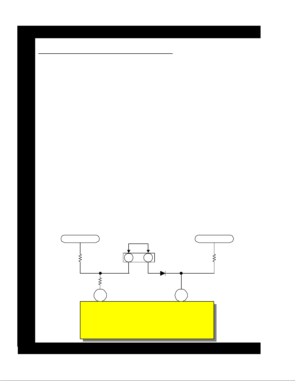
DP-1X MEMORY INITIALIZATION PROCEDURE (EEPROM RESET)
ow set to Air and not to Cable 1 or 2. No Child
WARNING: This should only be done in extreme cases. I2C Data will be reset as well.
Be sure and write down all data values before continuing.
NOTE: Sub Brightness and Horizontal Position for HD and Progressive will be reset to an incorrect value. Be sure to enter Service Menu, (with power off, press and hold the INPUT button, then press and hold POWER. I2C Service Menu will appear. The second selection is SUB
BRIT. Write this value down. On the Second page is H. POSI, write this value down in Progressive and in HD mode.
1) Disconnect Power to Television.
2) Remove the Back Cover.
3) Remove the two screws holding the Main chassis to the Cabinet if necessary.
4) Disconnect wiring harness clips to free up the chassis if necessary.
5) Reconnect Power to the Television and turn the set ON.
6) Locate PRST and add a jumper between pins 1 and 2 of the PRST connector as shown be-
low.
7) Hold jumper in place for 5 seconds. (A beep will NOT be heard).
8) Remove the jumper.
9) Confirm EEPROM reset, Input source is n
Lock, and only channels 2 through 13 are in memory.
10) Power Off
11) Reassemble Chassis and reinstall PTV back.
12) Enter the I2C Service Menu and re-enter the values for SUB BRIT and H.POSI
(Progressive and HD modes).
• Failure to re-enter these values will result in a dark picture and the horizontal centering will
be shifted off to the right. Convergence may be affected as well.
• DO NOT ATTEMPT TO CORRECT H. Centering with Convergence Adjustments.
• NOTE: All customers' Auto Programming and Set-Ups are returned to factory settings.
SBY +3.3V
Jumper
PRST
R176
2 1
Connector
R166
D008
8
KEY-IN2
CLOCK
I001
MicroProcessor
SBY +3.3V
R017
58
PAGE 01-17
DP-1X FACTORY RESET CONDITION
HITACHI USER CONTROL INITIALIZE (FACTORY RESET)
FUNCTION INITIAL DATA/CONDITION
NTSC Channel (Main, Sub) 03 CH
INPUT MODE Antenna A
SLEEP TIMER Not Registered
HELP MODE Off
MULTI WINDOW MODE Off
PIP Mode Single (Bottom Right)
Freeze Mode Single (Bottom Right)
SET UP
MENU LANGUAGE English
PLUG & PLAY —
ANTENNA/CABLE Antenna
CHANNEL MEMORY 2 ~ 13 CH
EDIT CHANNEL MEMORY - CLOCK SET Not Registered
MAGIC FOCUS - PICTURE FORMATS
ASPECT STYLE Aspect 1
V. POSITION 0
COMPOSITE COLOR TYPE SDTV/HD
VIDEO DISPLAY 1080i
CUSTOMIZE
NAME THE CHANNELS Not Registered
NAME THE INPUTS Not Registered
FAVORITE CHANNELS Not Registered
PARENTAL LOCKS Not Registered
PROGRAM TIMER Not Registered
CAPTION / DISPLAY Not Registered
CLOSED CAPTION
CCD DISPLAY Off
CCD MODE C.C.
CCD CHANNEL Channel 1
MENU BACKGROUND Shaded
VIDEO
CONTRAST 100%
BRIGHTNESS 50%
COLOR 50%
TINT Center
SHARPNESS 50%
ADVANCED SETTINGS
PERFECT PICTURE Off
AUTO COLOR On
NOISE REDUCTION Off
VELOCITY MODULATION On
BLACK LEVEL EXPANSION On
COLOR TEMPERATURE Cool
PAGE 01-18
DP-1X FACTORY RESET CONDITION
HITACHI USER CONTROL INITIALIZE (FACTORY RESET)
AUDIO INITIAL DATA/CONDITION
BASS 63%
TREBLE 50%
BALANCE Center
ADVANCED SETTINGS
MTS Mode Stereo
INTERNAL SPEAKERS On
AUTO NOISE CANCEL Off
LOUDNESS Off
PERFECT VOLUME Off
DYNAMIC BASS (DP17 Only) On
THEATER
THEATER MODE Sports
SURROUND
SRS On
BBE Off
SURROUND (DP16 Only)
TRUSURROUND/SRS/Off TruSurround
SURROUND (DP17 Only)
OFF/STADIUM/ROCK ARENA/JAZZ Standard
INPUT SOURCE (DP17 Only)
VID 4 Optical
VID 5 Coaxial
LISTENING POSITION Mid
LISTENING MODE Standard
SPEAKER SET UP (DP17 Only)
FRONT L/R Internal
SURROUND Yes
SUB WOOFER Yes
Analog
PAGE 01-19
PAGE 01-20
1. I2C Parameter List
(1) Adjust Mode OSD
Press POWER + INPUT
of control panel.
B CUT 3F
G CUT 3F
R CUT 3F
G DRV 3F
ADJUST MODE XXXXXXXX
SERVICE
SUB BRT*
WHITE BAL
R DRV (COOL)* 3F
B DRV (COOL)* 3F
R CUTOFF (COOL)* 80
G CUTOFF (COOL)* 80
B CUTOFF (COOL)* 80
H POSITION* 3F
V POSITION* 3F
FACT RESET
CH U/D, INPUT
ADJUST MODE
SERVICE
SUB BRT
WHITE BAL
R DRV (COOL) 48
B DRV (COOL) 37
R CUTOFF (COOL) 80
G CUTOFF (COOL) 80
B CUTOFF (COOL) 80
H POSITION 12
V POSITION 00
FACT RESET
CH U/D, INPUT
Select SERVICE
and press E key
Press EXIT key
(OSD OFF)
CUT OFF ADJUST MODE
ADJUST MODE
SERVICE
SUB BRT
WHITE BAL
R DRV (COOL) 3F
B DRV (COOL) 3F
R CUTOFF (COOL) 80
G CUTOFF (COOL) 80
B CUTOFF (COOL) 80
H POSITION 3F
V POSITION 3F
FACT RESET
CH U/D, INPUT
MENU
Select SERVICE
and press E key
Press EXIT key
R DRV 3F
MENU
MENU
Select SERVICE
and press E key
Press EXIT key
BRIGHTNESS 80
Press F E to adjust
VIDEO SETTINGS
(1) CONTRAST : MIN
(2) COLOR : MIN
VIDEO SETTINGS
(1) CONTRAST : MAX
(2 ) COLOR,TINT,SHARP,BRIGHT:CENER
(3) COLOR TEMP : COOL
ADJUST
(1) Press G H to select the G DRV.,
R DRV., R CUT, G CUT, B CUT.
(Initial position G/B DRV). G/B
DRV, B/R DRV select by the DR R
and DR BG.
(2) Press F E to adjust.
WHITE BALANCE
ADJ. MODE
POWER + INPUT
Only adjust
in cool mode.
Only adjust
in cool mode.
Only adjust
in cool mode.
*: Adjustable data
others: Fixed data (be careful not to change)
A
SUB BRIGHT
ADJ. MODE
G H
PAGE 01-21
ADJUST MODE
SERVICE
SUB BRT*
WHITE BAL*
G DRV (COOL)* 3F
R DRV (COOL)* 3F
R CUTOFF (COOL)* 80
G CUTOFF (COOL)* 80
B CUTOFF (COOL)* 80
H POSI (V/P)* 3F
47 VD-POS (FC)* 3F
FACT RESET
CH U/D, INPUT
CH U/D, INPUT
CH U/D, INPUT CH U/D, INPUT
CH U/D, INPUT
SELECT
SELECT
CH U/D, INPUT
WARM, NTSC, STD ADJ MODE
1. Press G H to select the G DRV or R DRV.
2. Press select to change the COOLRWARMR
NTSCRCOOL mode. Adjust on each mode,
but cannot adjust on the COOL mode.
3. WARM and NTSC mode data is offset data
based on the COOL mode data.
4. Do not adjust WHITE BALANCE in WARM or
NTSC mode. Adjust in COOL mode only.
CH U/D, INPUT
SELECT
MENU GH
SELECT
ADJUST MODE
SERVICE
SUB BRT*
WHITE BAL*
G DRV (COOL)* 48
R DRV (COOL)* 4F
R CUTOFF (COOL)* 80
G CUTOFF (COOL)* 80
B CUTOFF (COOL)* 80
H POSI (V/P)* 3F
47 VD-POS (FC)* 3F
FACT RESET
ADJUST MODE
SERVICE
SUB BRT*
WHITE BAL*
G DRV (COOL)* 4E
R DRV (COOL)* 58
R CUTOFF (COOL)* 80
G CUTOFF (COOL)* 80
B CUTOFF (COOL)* 80
H POSI (V/P)* 3F
47 VD-POS (FC)* 3F
FACT RESET
ADJUST MODE
SERVICE
SUB BRT*
WHITE BAL*
G DRV (COOL)* 3F
R DRV (COOL)* 3F
R CUTOFF (COOL)* 80
G CUTOFF (COOL)* 80
B CUTOFF (COOL)* 80
H POSI H* 3F
47 VD-POS (FC)H* 3F
FACT RESET
ADJUST MODE
SERVICE
SUB BRT*
WHITE BAL*
G DRV (COOL)* 3F
R DRV (COOL)* 3F
R CUTOFF (COOL)* 80
G CUTOFF (COOL)* 80
B CUTOFF (COOL)* 80
H POSI* 3F
47 VD-POS (FC)* 3F
FACT RESET
Other Mode 1080i throuth mode
Other Mode 1080i throuth mode
SELECT
Only adjust
in cool mode.
VD Position Adj Mode
Press F E to adjust
H Position Adj Mode
Press F E to adjust
PAGE 01-22
ADJUST MODE
YUVSEL RESET
3DYC RESET
1HV/C RESET
FLEX RESET
2HV/P RESET
BBE RESET
MEMORY INIT
I2COPEN
CH U/D, INPUT
Same data of
Main and Sub
ADJUST MODE
TA1270-M
TINT (TV) 3C
TOFF0 (TV) 00
TOFQ (TV) 00
SUB CNT 0F
SUB CLR 0F
CH U/D, INPUT
}
}
Press G H to select.
Press E to set to the
initial data of each
device.
Press G H to select.
Press E to set to the
initial or factory
settings.
MENU
G H
Item Device
YUVSEL CXA2141Q
3DYC uPD64082
1HV/C TA1270BF
FLEX FLEX CONT.
2HV/P TA1316AN
BBE NJW1132
ADJUST MODE
TA1270-S
TINT (TV) 3C
TOFF0 (TV) 00
TOFQ (TV) 00
SUB CNT 0F
SUB CLR 0F
SPLIT/SINGLE
MODE
+
PiP CH
SURF
mode
(ANT A only)
SPLIT
mode
SINGLE
mode
(NTSC only)
NORMAL
mode
PIP
ON/OFF
key
PIP
Mode
key
PIP
Mode
key
PIP Mode key
ADJUST MODE
CXA2151
MAT OUT 0
H WIDTH 0
V TC 1
HSEP 0
HS MASK 1
CH U/D, INPUT
ADJUST MODE
CXA2151
MACRO 1
GAIN SEL 0
CBGAIN 7
CRGAIN 7
YGAIN 7
CH U/D, INPUT
MENU GH
MENU GH
ADJUST MODE
UPD64082
DYGA 09
DCGA 06
VAPGA 00
VAPIN 0B
YHCOR 00
CH U/D, INPUT
MENU GH
MENU GH
MENU GH
 Loading...