

Page 1

SERVICE MANUAL
MANUEL D'ENTRETIEN
WARTUNGSHANDBUCH
CAUTION:
Before servicing this chassis, it is important that the service technician read the “Safety
Precautions” and “Product Safety Notices” in this service manual.
SM003
«MODEL NAMES»
32PD3000E
42PD3000E
Data contained within this Service
manual is subject to alteration for
improvement.
ATTENTION:
Avant d’effectuer l’entretien du châassis, le technicien doit lire les «Précautions de sécurité»
et les «Notices de sécurité du produit» présentés dans le présent manuel.
VORSICHT:
Vor Öffnen des Gehäuses hat der Service-Ingenieur die „Sicherheitshinweise“ und „Hinweise
zur Produktsicherheit“ in diesem Wartungshandbuch zu lesen.
Les données fournies dans le présent
manuel d’entretien peuvent faire l’objet
de modifications en vue de perfectionner
le produit.
Die in diesem Wartungshandbuch
enthaltenen Spezifikationen können sich
zwecks Verbesserungen ändern.
SPECIFICATIONS AND PARTS ARE SUBJECT TO CHANGE FOR IMPROVEMENT
Plasma TV
October 2002
Page 2

Safety
ENGLISH
SAFETY PRECAUTIONS
WARNING: The following precautions must be
observed.
ALL PRODUCTS
Before any service is performed on the chassis an
isolation transformer should be inserted between
the power line and the product.
1. When replacing the chassis in the cabinet,
ensure all the protective devices are put back in
place.
2. When service is required, observe the original
lead dressing. Extra precaution should be taken to
ensure correct lead dressing in any high voltage
circuitry area.
3. Many electrical and mechanical parts in
HITACHI products have special safety related
characteristics. These characteristics are often not
evident from visual inspection, nor can the
protection afforded by them necessarily be
obtained by using replacement components rated
for higher voltage, wattage, etc. Replacement parts
which have these special safety characteristics are
identified by marking with a ! on the schematics
and the replacement parts list. The use of a
substitute replacement component that does not
have the same safety characteristics as the
HITACHI recommended replacement one, shown
in the parts list, may create electrical shock, fire, Xradiation, or other hazards.
4. Always replace original spacers and maintain
lead lengths. Furthermore, where a short circuit has
occurred, replace those components that indicate
evidence of overheating.
5. Insulation resistance should not be less than 2M
ohms at 500V DC between the main poles and any
accessible metal parts.
6. No flashover or breakdown should occur during
the dielectric strength test, applying 3kV AC or
4.25kV DC for two seconds between the main
poles and accessible metal parts.
7. Before returning a serviced product to the
customer, the service technician must thoroughly
test the unit to be certain that it is completely safe
to operate without danger of electrical shock. The
service technician must make sure that no
protective device built into the instrument by the
manufacturer has become defective, or
inadvertently damaged during servicing.
32PD3000 / 42PD3000
CE MARK
1. HITACHI products may contain the CE mark on
the rating plate indicating that the product contains
parts that have been specifically approved to
provide electromagnetic compatibility to designated
levels.
2. When replacing any part in this product, please
use only the correct part itemised in the parts list to
ensure this standard is maintained, and take care
to replace lead dressing to its original state, as this
can have a bearing on the electromagnetic
radiation/immunity.
PICTURE TUBE
1. The line output stage can develop voltages in
excess of 25kV; if the E.H.T. cap is required to be
removed, discharge the anode to chassis via a high
value resistor, prior to its removal from the picture
tube.
2. High voltage should always be kept at the rated
value of the chassis and no higher. Operating at
higher voltages may cause a failure of the picture
tube or high voltage supply, and also, under certain
circumstances could produce X-radiation levels
moderately in excess of design levels. The high
voltage must not, under any circumstances, exceed
29kV on the chassis (except for projection
Televisions).
3. The primary source of X-radiation in the product
is the picture tube. The picture tube utilised for the
above mentioned function in this chassis is
specially constructed to limit X-radiation. For
continued X-radiation protection, replace tube with
the same type as the original HITACHI approved
type
4. Keep the picture tube away from the body while
handling. Do not install, remove, or handle the
picture tube in any manner unless shatterproof
goggles are worn. People not so equipped should
be kept away while picture tubes are handled
LASERS
If the product contains a laser avoid direct
exposure to the beam when the cover is open or
when interlocks are defeated or have failed.
1
Page 3

32PD3000 / 42PD3000
FRANÇAIS
CONSIGNES DE SECURITE
AVERTISSEMENT: vous devez respecter les
précautions suivantes
POUR TOUS LES PRODUITS
d’effectuer une intervention d’entretien sur le
châssis, vous devez insérer un transformateur
d’isolement entre la ligne d’alimentation électrique
et le produit.
1. Lors de la remontage du châssis dans le coffret,
vérifiez que tous les dispositifs de protection sont
remis en place.
2. Lorsqu’une intervention d’entretien s’avère
nécessaire, respectez l’agencement d’origine des
conducteurs. Vous devez prendre des precautions
supplémentaires pour garantir un agencement
correct des conducteurs dans toutes les zones où
des circuits haute tension sont présents.
3. De nombreux composants électriques et
mécaniques des appareils HITACHI ont des
caractéristiques spéciales de sécurité. Bien
souvent, ces caractéristiques ne sont pas
évidentes lors d’un examen visuel et la protection
qu’ils offrent n’est pas forcément garantie si vous
utilisez des composants de rechange conçus, par
exemple, pour une tension plus élevée, une
puissance plus forte. Les pièces de rechange qui
offrent des caractéristiques spéciales de sécurité
sont identifiées par un repérage comportant le
symbole ! sur les schémas et sur la nomenclature
des pièces de rechange. L’emploi d’un composant
de rechange qui ne respecte pas les mêmes
caractéristiques de sécurité que la pièce de
rechange que recommande HITACHI et qui figure
dans la nomenclature risque de provoquer un choc
électrique, un incendie, des rayons X ou d’autres
dangers.
4. Remettez toujours en place les entretoises
d’origine et respectez la longueur des conduites.
En outre, à la suite d’un court-circuit, remplacez les
composants présentant des signes de surchauffe.
5. La résistance d’isolement doit être supérieure ou
égale à 2 méga ohms à 500 V c.c. entre les poles
principaux et des composants métalliques
accessibles, quels qu’ils soient.
6. Aucun claquage et aucune rupture ne doit se
produire pendant l’essai de résistance diélectrique
à la suite de l’application d’une tension de 3 kV c.a.
ou de 4,35 kV c.c. pendant deux secondes entre
les poles principaux et des composants métalliques
accessibles.
7. Avant de remettre au client un produit qui a fait
l’objet d’un entretien, le technicien qui s’est chargé
de cette intervention doit tester à fond cet
ensemble pour s’assurer qu’il ne présente aucun
danger opérationnel et aucun risque de choc
électrique. Ce technicien doit s’assurer qu’aucun
des dispositifs de protection intégrés à cet
instrument par le fabricantn’est défectueux ou n’a
été endommagé de façon accidentelle lors de
l’entretien. suivantes
Avant
LABEL CE
1. Les produits HITACHI peuvent avoir reçu le label
CE qui figure sur la plaque signalétique pour
indiquer que cet ensemble contient des
composants qui ont fait l’objet d’une homologation
spécifique de respect des normes de compatibilité
électromagnétique en fonction de niveaux bien
spécifiés.
2. Lors du remplacement d’un des composants de
ce produit, utilisez uniquement le composant
correct identifié dans la nomenclature afin de
maintenir le respect de cette norme ; en outre, vous
devez également ramener l’agencement des
conducteurs à son état d’origine car cela peut avoir
une influence au niveau des rayonnements
électromagnétiques et sur la protection contre ces
rayons.
PICTURE TUBE
1. L’étage de sortie des lignes peut développer des
tensions de plus de 25 kV ; s’il faut retirer le
chapeau de protection contre les tensions
extrêmement élevées, il convient de décharger
l’anode contre le châssis par le biais d’une
résistance de forte valeur avant de déposer ce
chapeau du tube image.
2. La haute tension doit toujours se maintenir à la
valeur nominale du châssis et ne pas dépasser
cette dernière. Un fonctionnement à des
températures élevées peut provoquer une
défaillance du tube image ou l’entrée d’une tension
élevée. Dans certains cas, cela peut même
provoquer des rayons X d’un niveau légèrement
supérieur aux valeurs de calcul. Cette haute
tension ne doit en aucun cas dépasser 29 kV sur le
châssis (à l’exception des téléviseurs de
projection).
3. La principale source de rayons X de cet appareil
est le tube image. Le tube image employé pour
assurer la fonction susmentionnée dans ce châssis
est spécialement construit pour limiter des rayons
X. Pour maintenir cette protection contre les rayons
X, il faut remplacer le tube d’origine d’un type agréé
par HITACHI par un autre tube de même type.
4. Lors des manipulations, ne tenez jamais le tube
image contre le corps. Pendant toutes les
operations d’installation, de dépose et de
manipulation de ce tube image, quelle que soit la
méthode employée, vous devez toujours porter des
lunettes de sécurité anti-éclatements. Les
personnes qui ne portent pas ce type de lunettes
doivent se tenir à l’écart du tube image lors de la
manipulation de ce dernier.
RAYONS LASER
Si ce produit contient un rayon laser, évitez toute
exposition directe à ce faisceau lors de l’ouverture
du couvercle ou lors de l’élimination des
verrouillages de sécurité ou après défaillance de
ces verrouillages.
2
Page 4

DEUTSCH
SICHERHEITSVORKEHRUNGEN
WARNUNG: Die folgenden Vorkehrungen müssen
eingehalten werden.
ALLE PRODUKTE
gewartet wird, sollte ein Trenntrafo zwischen die
Netzleitung und das Produkt eingebracht werden.
1. Wenn die Grundplatte in das Gehäuse
zurückgestellt wird, stellen Sie sicher, dass alle
Schutzvorrichtungen wieder an ihrem Ort sind.
2. Wenn Wartung erforderlich ist, halten Sie die
originale Verdrahtungsart ein. Besondere Vorsicht
ist nötig, um die korrekte Verdrahtungsart in jedem
Hochspannungsstromkreis zu gewährleisten.
3. Viele elektrische und mechanische Teile von
HITACHI Produkten haben besondere
sicherheitsbezogene Eigenschaften. Diese
Eigenschaften fallen oft nicht ins Auge, aber der
durch sie gewährte Schutz kann nicht unbedingt
erreicht werden, wenn man Ersatzteile benutzt, die
für höhere Spannung, Leistung usw. ausgelegt
sind. Ersatzteile, die diese besonderen
Sicherheitsmerkmale haben, sind in den
Prinzipskizzen und Ersatzteillisten an einem ! zu
erkennen. Der Gebrauch von Ersatzteilen, die nicht
dieselben Sicherheitsmerkmale haben wie die
empfohlenen HITACHI Ersatzteile, wie sie in der
Ersatzteilliste aufgeführt sind, kann zu elektrischem
Schlag, Feuer, Röntgenstrahlung und anderen
Gefahren führen.
4. Immer die originalen Abstandsstücke ersetzen
und die Leitungslängen beibehalten. Wo ein
Kurzschluss passiert ist, die Teile ersetzen, bei
denen Überhitzung nachzuweisen ist.
5. Der Isolierwert sollte bei 500 V Gleichstrom
zwischen den Hauptpolen und allen zugänglichen
Metallteilen nicht unter 2M Ohm liegen.
6. Bei der Prüfung auf Durchschlagsfestigkeit sollte
kein Überschlag oder Durchschlag vorkommen,
wenn zwei Sekunden lang 3 kV Wechselstrom oder
4,25 kV Gleichstrom zwischen den Hauptpolen und
allen zugänglichen Metallteilen angelegt wird.
7. Bevor das gewartete Produkt dem Kunden
zurückgegeben wird, muss der Wartungstechniker
das Gerät gründlich prüfen, um sicherzustellen,
dass es betriebssicher ist ohne das Risiko eines
elektrischen Schlages. Der Wartungstechniker
muss sicherstellen, dass keine vom Hersteller im
Gerät eingebaute Schutzvorkehrung schadhaft
geworden ist oder bei der Wartung unabsichtlich
beschädigt wurde.
CE KENNZEICHEN
1. HITACHI Produkte enthalten eventuell das CE
Kennzeichen auf dem Leistungsschild, welches
angibt, dass das Produkt Teile enthält, die eigens
zugelassen sind, um bis zu einem spezifizierten
Niveau elektromagnetische Störfreiheit zu
bewirken.
2. Wenn Sie irgendein Teil in diesem Produkt
ersetzen, benutzen Sie bitte nur das korrekte Teil,
das in der Ersatzteilliste aufgeführt ist, um
sicherzustell en, dass dieser Standard eingehalten
Bevor die Grundplatte
32PD3000 / 42PD3000
wird, und geben Sie acht, die Verdrahtungsart in
ihren ursprünglichen Zustand zurück zu versetzen,
weil das einen Einfluss auf die elektromagnetische
Abstrahlung/Störsicherheit haben kann.
BILDRÖHRE
1. Die Leitungsausgangsstufe kann Spannungen
von mehr als 25 kV entwickeln; wenn die
Höchstspannungskappe entfernt werden muss,
entladen Sie die Anode zum Gehäuse über einen
hochohmigen Widerstand, bevor Sie sie aus der
Bildröhre entfernen.
2. Hochspannung sollte immer auf den festgelegten
Wert des Gehäuses beschränkt bleiben und nicht
mehr. Betrieb bei höherer Spannung kann zum
Versagen der Bildröhre oder zu hoher
Spannungszufuhr führen und kann unter
Umständen auch Röntgenstrahlung hervorbringen,
die leicht über dem Konstruktionsniveau liegt. Die
Hochspannung darf auf keinen Fall 29 kV am
Gehäuse überschreiten (außer bei
Projektionsfernsehern).
3. Die Hauptquelle der Röntgenstrahlung im
Produkt ist die Bildröhre. Die Bildröhre, die für die
oben erwähnte Funktion in diesem Gehäuse
benutzt wird, ist eine Spezialkonstruktion zur
Begrenzung der Röntgenstrahlung. Um den Schutz
vor der Röntgenstrahlung zu behalten, ersetzen Sie
bitte die Röhre durch denselben Typ wie den
ursprünglichen von HITACHI zugelassenen.
8. Halten Sie die Bildröhre bei der Handhabung
vom Körper weg. Sie dürfen die Bildröhre nur dann
installieren, entfernen oder handhaben, wenn Sie
eine nicht splitternde Schutzbrille tragen. Personen
ohne
derartigen Schutz sollten ferngehalten werden,
solange Bildröhren gehandhabt werden.
LASER
Wenn das Produkt einen Laser enthält, setzen Sie
sich keinesfalls direkt dem Strahl aus, wenn die
Abdeckung geöffnet ist oder wenn die Verriegelung
versagt.
3
Page 5

32PD3000 / 42PD3000
Contents
Safety .......................................................................................................................................................1
ENGLISH ............................................................................................................................................1
FRANÇAIS.......................................................................................................................................... 2
DEUTSCH ...........................................................................................................................................3
Contents ...................................................................................................................................................4
Lead Free Solder ......................................................................................................................................6
Specifications...........................................................................................................................................7
General Specifications .........................................................................................................................7
Features ;..............................................................................................................................................8
Service Data .............................................................................................................................................9
Block Diagrams .....................................................................................................................................16
AVC to PDP Block Diagram .............................................................................................................16
AVC Block Diagram..........................................................................................................................17
AVC Power Block Diagram ..............................................................................................................18
Major Connectors...............................................................................................................................19
Monitor Block Diagram.....................................................................................................................20
Schematic Drawing Descriptions...........................................................................................................21
Schematic Page 1 ; Tuner / Video Chroma........................................................................................21
Schematic Page 2 ; Sound / AV3 Control..........................................................................................23
Schematic Page 3 ; Interface Board (component input, progressive sync separation, centre audio
channel)..............................................................................................................................................25
Schematic Page 4 ; Power Circuit (Voltage Regulator) / Level Shifter ...........................................27
Schematic Page 5 ; Micro Controller.................................................................................................28
Schematic Page 6 ; COMB Filter / SVHS Output .............................................................................29
Schematic Page 7 ; SCART / FC-MSC Connection..........................................................................30
Schematic; AVC Power Supply.........................................................................................................32
Schematic Drawings ..............................................................................................................................33
Schematic Sheet 1 ..............................................................................................................................33
Schematic Sheet 2 ..............................................................................................................................34
Schematic Sheet 3 ..............................................................................................................................35
Schematic Sheet 4 ..............................................................................................................................36
Schematic Sheet 5 ..............................................................................................................................37
Schematic Sheet 6 ..............................................................................................................................38
Schematic Sheet 7 ..............................................................................................................................39
AV Power Schematic.........................................................................................................................40
AV Control Schematic.......................................................................................................................41
Signal / Sound Sheet 1 .......................................................................................................................42
Signal / Sound Sheet 2 .......................................................................................................................43
Signal / Sound Sheet 3 .......................................................................................................................44
Signal / Sound Sheet 4 .......................................................................................................................45
Filter, LED, Switch & Speakers ........................................................................................................46
Circuit Boards ........................................................................................................................................47
AV Board Side A ...............................................................................................................................47
AV Board Side B ...............................................................................................................................48
AV Power Side A...............................................................................................................................49
AV Power Side B...............................................................................................................................50
Signal / Sound Board Side A .............................................................................................................51
Signal / Sound Board Side B .............................................................................................................52
Filter, LEDs, Speaker PCBs...............................................................................................................53
Troubleshooting Flow Charts ................................................................................................................54
4
Page 6

32PD3000 / 42PD3000
AV Power - 1 .....................................................................................................................................54
AV Power - 2 .....................................................................................................................................55
AV Power - 3 .....................................................................................................................................56
AV Circuit..........................................................................................................................................57
Assembly Drawings ...............................................................................................................................58
Audio / Video.....................................................................................................................................58
Wiring for Audio / Video Components .............................................................................................59
Monitor Front View ...........................................................................................................................60
Monitor Rear View ............................................................................................................................61
32 inch Monitor Wiring A .................................................................................................................62
32 inch Monitor Wiring B..................................................................................................................63
42 inch Monitor Wiring A .................................................................................................................64
42 inch Monitor Wiring B..................................................................................................................65
24way Digital Interface Cable Connection............................................................................................66
Microprocessor Pins...............................................................................................................................67
Connections to FC4................................................................................................................................69
PCB Connectors..................................................................................................................................... 72
Replacement Parts..................................................................................................................................73
Signal / Sound Board .........................................................................................................................73
Filter Board ........................................................................................................................................75
32PD3000 ..........................................................................................................................................76
42PD3000 ..........................................................................................................................................77
Questions & Answers ............................................................................................................................79
5
Page 7

32PD3000 / 42PD3000
Lead Free Solder
This product uses lead free (unleaded) solder to help preserve the environment. Please read these instructions
before attempting any soldering work.
Caution: Always wear safety glasses to prevent fumes or molten solder from getting into the eyes. Lead free
solder can splatter at high temperatures (600 °C).
• Lead free solder indicator
Printed circuit board Assemblies using lead free solder shown below are engraved with an "F" following
Board Name.
• Properties of lead free solder
The melting point of lead free solder is 40-50 °C higher than one of leaded solder.
•
When servicing solder
o Solder with an alloy composition of Sn-3.0Ag-0.5Cu or Sn-0.7Cu is recommended.
o Although servicing with leaded solder is possible, there are a few precautions that have to be
taken.(Not taking these precautions may cause the solder not to harden properly and lead to
consequent malfunctions.)
• Precautions when using leaded solder
o
Remove all lead free solder from soldered joints when replacing components.
o
If leaded solder should be added to existing lead free joints, mix in the leaded solder thoroughly
after the lead free solder has been completely melted (do not apply the soldering iron without
adding solder).
When servicing soldering iron
A soldering iron with a temperature setting capability (temperature control function)is recommended.
The melting point of lead free solder is higher than one of leaded solder. Use a soldering iron that maintains a
high stable temperature (large heat capacity),and that allows temperature adjustment according to the part
being serviced, to avoid poor servicing performance.
Recommended soldering iron:
Soldering iron with temperature control function (temperature range:320-450 °C)
Recommended temperature range per part:
Soldering Part
PCB with surface mount devices
PCB without surface mount devices
Chassis, metallic shield, etc.
PCBs which use lead free solder
• FC4PDP board (AVC block)
• SIGNAL/SOUND board (MONITOR block)
• SP terminal L/R board, FILTER board, LED board (MONITOR block)
Soldering iron temperature
320 °C ±30 °C
380 °C ±30 °C
420 °C ±30 °C
6
Page 8

32PD3000 / 42PD3000
Specifications
General Specifications
Spec Item
32PD3000 (PDP;32PD3000E+AVC;AV3000E) 42PD3000 (PDP;42PD3000E+AVC;AV3000E)
PDP panel 32" (ALSI for mat) Plasma display panel (16:9) ,
resolution 852(H) x1024(V)
Display size 976(W) x 258(D) x 580(H) unit: mm 1233(W) x 300(D) x 713(H) unit: mm
Sound output
level
Speaker 4 x 16 cm corn type x 2 ???
Power supply AC 220 - 240 V 50Hz AC 220 - 240 V 50Hz
Power
consumption
Colour system PAL/SECAM/NTSC4.43/NTSC3.58/PAL60 PAL/SECAM/NTSC4.43/NTSC3.58/PAL60
Sound system I/B.G.H/LL' I/B.G.H/LL'
Tuning freq. 45MHz ~ 889MHz, VHF low/VHF
Position
selection
PC input
signal
AV input
Dimensions
Remote
control
batteries
Max. 10W x 2 (6 ohm) Max. 12W x 2 (6 ohm)
PDP 260W (stand-by <2W) AVC 30W, (standby <2W)
high/Hyper/UHF
100 (0~99) positions. Plus channel direct (C--/S-
-) and frequency direct (---.--MHz)
Horizontal freq. 24KHz ~ 109KHz / Vertical freq.
50Hz ~ 85Hz
Analogue RGB, input voltage 0.7Vpp/1.0Vpp
selectable
H/V separate sync (TTL level) *** sound input ;
common with AV3 or AV4
SCART101 (CVBS/SVHS/LR sound) - AV1 SCART101 (CVBS/SVHS/LR sound) - AV1
SCART102 (CVBS/RGB/LR sound) - AV2 SCART102 (CVBS/RGB/LR sound) - AV2
SCART100 (CVBS/RGB/LR sound) - AV3 SCART100 (CVBS/RGB/LR sound) - AV3
COMPONENT (YPbPr/YCbCr/LR sound) - AV4 COMPONENT (YPbPr/YCbCr/LR sound) - AV4
Front AV (CVBS/SVHS/LR sound) - FRONT Front AV (CVBS/SVHS/LR sound) - FRONT
CENTRE AUDIO input CENTRE AUDIO input
PDP : 974(W) x 256(D) x 578(H) including
monitor stand unit: mm
AVC : 430(W) x 293(D) x 121(H) unit: mm AVC : 430(W) x 293(D) x 121(H) unit: mm
PDP : 28.7kg (net) PDP : 40.2kg (net) Weight
AVC : 3.2kg (net) AVC : 3.2kg (net)
2 x Hitachi R6P(G) * equivalent 'AA' 2 x Hitachi R6P(G) * equivalent 'AA'
42" (ALSI for mat) Plasma display panel (16:9) ,
resolution 1024(H) x1024(V)
PDP 360W (stand-by <2W) AVC 30W, (standby <2W)
45MHz ~ 889MHz, VHF low/VHF
high/Hyper/UHF
100 (0~99) positions. Plus channel direct (C--/S-
-) and frequency direct (---.--MHz)
Horizontal freq. 24KHz ~ 109KHz / Vertical freq.
50Hz ~ 85Hz
Analogue RGB, input voltage 0.7Vpp/1.0Vpp
selectable
H/V separate sync (TTL level) *** sound input ;
common with AV3 or AV4
PDP : 1030(W) x ??(D) x 636(H) including
monitor stand unit: mm
7
Page 9

32PD3000 / 42PD3000
Features
852x1024 resolution,
1024x1024 resolution,
Advanced progressive & 1024 interlace,
TruBass by SRS,
Thin (9cm) and light,
Swivel stand attached monitor,
3 Scarts connectors plus front AV input,
1 Component input,
PC input connection,
;
Created by 32" ALIS Plasma display panel
Created by 37/42" ALIS Plasma display panel
Which materializes detailed picture without flicker
Which gives real bass sound
By separating monitor from tuner box (AVC). It is possible to hang
monitor on the wall.
Which is possible to swivel at 30deg toward left and right.
Which can be connected with DVD, Set Top Box, VCR and
Camera at the same time.
Which allows YPbPr and PCbCr to be received. Signal is
automatically identified.
Supporting various PC display format.
8
Page 10

32PD3000 / 42PD3000
Service Data
Soft version issue 1 New panel 01-Nov-02 V1.A4
back ground CYAN means to separate data on each 32/37/42"
32"
1st 2nd 3rd 4th 5th
SVC> TUN> ADC
OPT
AGC
BIF
LIF
AFC
PC> PC1> GSW
PC2> MBC
PC3> PSE
SIG> FLA
MAX
MIN
SNR
MIS> RGB > COL> R1 read read read
BLP
COP
MCC
MXB
BGP
CCP
DCP
PST
G1 read read read
B1 read read read
NOM> R2 read read read
G2 read read read
B2 read read read
WAM> R3 read read read
G3 read read read
B3 read read read
GSW
WHB
HAPC
BRN
37"
values
values
hex
hex
read read read
80 80 80
adj adj adj
adj adj adj
adj adj adj
read read read
01 01 01
7F 7F 7F
7F 7F 7F
7F 7F 7F
5D 5D 5D
6C 6C 6C
00 00 00
00 00 00
01 01 01
01 01 01
0F 0F 0F
OK OK OK
read read read
read read read
read read read
01 01 01
00 00 00
01 01 01
01 01 01
RED figures are new default
values
42"
values
hex
AGC data
option for destination
AGC adjustment
AFC adjustment for all except
L'
AFC adjustment for L'
AFC level indication
gamma switch PDP 10 D3:D2
Black Level (RGB);user
brightness control for PC
Contrast (RGB) FC4 6 D07:D00
main brightness centre FC4 7 D15:D08
main contrast centre FC4 7 D07:D00
brightness Max. for wide
NORMAL/REAL
Brightness/Gradation PDP 27&28 D2&D2
NTSC/EBU PDP 27&28 D1&D1
Tracking correction PDP 27&28 D0&D0
PC power save enable/disable FC4 4 D08
power save timer
CAUTION !! Never press OK
unless proper signal is
displayed. auto signal level
adjustment activates.
MAX signal level on screen
min. signal level on screen
FC noise level indication
Gain R ; warm
Gain G ; warm
Gain B ; warm
Gain R ; normal
Gain G ; normal
Gain B ; normal
Gain R ; cool
Gain G ; cool
Gain B ; cool
gamma switch PDP 10 D3:D2
white balance 0;cool, 1;normal,
2;warm --- synchronizing with
user operation MENU
Q.MODE + Heat APC PDP 28 D4:D3
burn in mode PDP 10 D5:D4
functions Device
FC4 5 D07:D00
FC4 7 D15:D08
PDP
Read/Write
PDP
Read/Write
PDP
Read/Write
PDP
Read/Write
PDP
Read/Write
PDP
Read/Write
PDP
Read/Write
PDP
Read/Write
PDP
Read/Write
PDP 9 D3:D2&D1:D0
13/20
13/21
13/22
12/17
12/18
12/19
11/14
11/15
11/16
1st D7:D0 /
D7:D0
2nd D7:D0 /
D7:D0
3rd D7:D0 /
D7:D0
1st D7:D0 /
D7:D0
2nd D7:D0 /
D7:D0
3rd D7:D0 /
D7:D0
1st D7:D0 /
D7:D0
2nd D7:D0 /
D7:D0
3rd D7:D0 /
D7:D0
9
Page 11

32PD3000 / 42PD3000
1st 2nd 3rd 4th 5th
*** MAX 8 items on one page.
*** LTI ***
picture mode
*** LTI ***
picture mode
MI0> M01> F01(4:3) 01 01 01
***
"PDP2_service05"
no.52
APC
F02(16:9) 00 00 00
F03(C16:9L) 00 00 00
F04(T16:9L) 01 01 01
F05(14:9) 01 01 01
M02> F06(C14:9L) 00 00 00
F07(T14:9L) 01 01 01
F08(PAN) 01 01 01
F09(14:9LS) 00 00 00
PCA 02 02 02
M03> HE1 02 02 02
HE2 03 03 03
HE3 00 00 00
HE4 00 00 00
HE5 01 01 01
HE6 02 02 02
HET 00 00 00 Horizontal enhancer TEXT
M04 VE1 03 03 03
VE2 03 03 03
VE3 03 03 03
VE4 03 03 03
VE5 03 03 03
VE6 03 03 03
VET 00 00 00 Vertical enhancer TEXT
M05> BGT 00 00 00
CCT 00 00 00
TCR 01 01 01
DCC 00 00 00
WBC 00 00 00
BSO 1F 1F 1F
SPC 00 00 00
M06> PHC 80 80 80
PHU 1A 1A 1A
NHU 20 20 20
YU6 1D 1D 1D
32"
37"
values
values
hex
00 00 00
values
hex
42"
hex
APC switch 0;High APC,
1;Normal
wide mode selected by 16:9
key (0;on, 1;off)
wide mode selected by 16:9
key (0;on, 1;off)
wide mode selected by 16:9
key (0;on, 1;off)
wide mode selected by 16:9
key (0;on, 1;off)
wide mode selected by 16:9
key (0;on, 1;off)
wide mode selected by 16:9
key (0;on, 1;off)
wide mode selected by 16:9
key (0;on, 1;off)
wide mode selected by 16:9
key (0;on, 1;off)
wide mode selected by 16:9
key (0;on, 1;off)
PC wide mode 0;NORMAL,
1;REAL, 2;FULL
Horizontal enhancer
DYNAMIC
Horizontal enhancer
DYNAMIC-VIDEO
Horizontal enhancer
NATURAL
Horizontal enhancer
NATURAL-VIDEO
Horizontal enhancer CINEMA FC4 2 D20:D19
Horizontal enhancer CINEMAVIDEO
Vertical enhancer DYNAMIC FC4 2 D22:D21
Vertical enhancer DYNAMICVIDEO
Vertical enhancer NATURAL FC4 2 D22:D21
Vertical enhancer NATURALVIDEO
Vertical enhancer CINEMA FC4 2 D22:D21
Vertical enhancer CINEMAVIDEO
Brightness/Gradation PDP 27&28 D2&D2
NTSC/EBU PDP 27&28 D1&D1
Tracking correction W/B
Warm & Norm
Tracking correction W/B Cool PDP 27&28 D0&D0
Black Stretch gain offset
ON&MID
PinP(PC W) picture contrast
offset
Colour phase centre FC4 8 D07:D00
PAL HUE offset (not available
if AV2 is RGB)
NTSC HUE offset FC4 8 D07:D00
YCbCr / YPbPr @ 60Hz HUE
offset
functions Device
PDP 10 D7
4:3
WIDE
SCREEN
LETTERBOX
T16:9L
14:9
C14:9L
T14:9L
PANORAMIC
14:9 ZOOM
FC4 3 D17:D16
FC4 2 D20:D19
FC4 2 D20:D19
FC4 2 D20:D19
FC4 2 D20:D19
FC4 2 D20:D19
FC4 2 D20:D19
FC4 2 D22:D21
FC4 2 D22:D21
FC4 2 D20:D19
FC4 2 D22:D21
PDP 27&28 D0&D0
FC4 7 D21:D16
FC4 7 D07:D00
FC4 8 D07:D00
FC4 8 D07:D00
10
Page 12

1st 2nd 3rd 4th 5th
*** CTI ***
picture mode
*** YNR ***
picture mode
*** CNR ***
picture mode
MI1> M11> BLT 7F 7F 7F
YU5 1A 1A 1A
THU 1F 1F 1F
YHU 1F 1F 1F
FPB 00 00 00
MBC 80 80 80
MBX 80 80 80
COT 7F 7F 7F
MCC 89 89 89
MCX 70 70 70
SAC 40 40 40
SAX 50 50 50
M12> CE1 1F 1F 1F
CE2 10 10 10
CE3 1F 1F 1F
CE4 10 10 10
CE5 1F 1F 1F
CE6 10 10 10
CET 10 10 10
YET 00 00 00 sharpness centre - TEXT
M13> YE1 1F 1F 1F
YE2 12 12 12
YE3 12 12 12
YE4 12 12 12
YE5 12 12 12
YE6 12 12 12
YE7 12 12 12
YE8 12 12 12
M14> YI1 01 01 01
YI2 01 01 01
YI3 01 01 01
YI4 01 01 01
YI5 01 01 01
YI6 01 01 01
YIT 01 01 01 YNR input gain TEXT
M15> CI1 00 00 00
CI2 00 00 00
CI3 00 00 00
CI4 00 00 00
CI5 00 00 00
32"
values
hex
37"
values
hex
32PD3000 / 42PD3000
42"
values
hex
YCbCr / YPbPr @ 50Hz HUE
offset
TEXT HUE offset FC4 8 D07:D00
Components Hue for Asian
option
FAVOURITE Peak Brightness
0;Peak, 1:Normal
Black level (RGB) FC4 5 D07:D00
main brightness centre : (50) is
used in AUTO adjustment
brightness centre TEXT FC4 7 D15:D08
Contrast (RGB) FC4 6 D07:D00
main contrast centre FC4 7 D07:D00
contrast centre TEXT FC4 7 D07:D00
Saturation centre
NTSC/PAL/RGB/YCbCr TV
Saturation centre TEXT FC4 8 D14:D08
C-Vert/Horiz enhancer gain
DYNAMIC-TV
C-Vert/Horiz enhancer gain
DYNAMIC-VIDEO
C-Vert/Horiz enhancer gain
NATURAL-TV
C-Vert/Horiz enhancer gain
NATURAL-VIDEO
C-Vert/Horiz enhancer gain
CINEMA-TV
C-Vert/Horiz enhancer gain
CINEMA-VIDEO
C-Vert/Horiz enhancer gain
TEXT
sharpness DYNAMIC-TV FC4 2 D04:D00
sharpness DYNAMICTVIDEO
sharpness NATURAL-TV FC4 2 D04:D00
sharpness NATURAL-VIDEO FC4 2 D04:D00
sharpness CINEMA-TV FC4 2 D04:D00
sharpness CINEMA-VIDEO FC4 2 D04:D00
sharpness centreFAVOURITE-TV
sharpness centreFAVOURITE-VIDEO
YNR input gain DYNAMIC FC4 2 D07:D05
YNR input gain DYNAMICVIDEO
YNR input gain NATURAL FC4 2 D07:D05
YNR input gain NATURALVIDEO
YNR input gain CINEMA FC4 2 D07:D05
YNR input gain CINEMAVIDEO
CNR input gain DYNAMIC FC4 2 D15:D13
CNR input gain DYNAMICVIDEO
CNR input gain NATURAL FC4 2 D15:D13
CNR input gain NATURALVIDEO
CNR input gain CINEMA FC4 2 D15:D13
functions Device
FC4 8 D07:D00
FC4 8 D07:D00
PDP 10 D6
FC4 7 D15:D08
FC4 8 D14:D08
FC4 2 D12:D08
FC4 2 D12:D08
FC4 2 D12:D08
FC4 2 D12:D08
FC4 2 D12:D08
FC4 2 D12:D08
FC4 2 D12:D08
FC4 2 D04:D00
FC4 2 D04:D00
FC4 2 D04:D00
FC4 2 D04:D00
FC4 2 D07:D05
FC4 2 D07:D05
FC4 2 D07:D05
FC4 2 D07:D05
FC4 2 D15:D13
FC4 2 D15:D13
11
Page 13

32PD3000 / 42PD3000
32"
37"
1st 2nd 3rd 4th 5th
[ ];menu related value - decimal
it is ok to display by hex
e.g. [32] is centre of CONTRAST
e.g. [63] is MAX for
CONTRAST.
MI2> M21> DCN 3E 3E 3E
MI3> M31> MVB 0B 0B 0B
CI6 00 00 00
CIT 00 00 00 CNR input gain TEXT
M16 OSH 109 109 109
OSV 40 40 40
OTH 190 190 190
OTV 40 40 40
SUR 00 00 00
CMB 01 01 01
DBR 80 80 80
DCL 50 50 50
DPB 00 00 00
DCM 02 02 02
DBS 1F 1F 1F
DWB 00 00 00
DFT 01 01 01
M22> NCN 38 38 38
NBR 80 80 80
NCL 48 48 48
NPB 00 00 00
NCM 01 01 01
NBS 1A 1A 1A
NWB 00 00 00
NFT 01 01 01
M23> TCN 3E 3E 3E
TBR 80 80 80
TCL 50 50 50
TPB 00 00 00
TCM 00 00 00
TBS 1F 1F 1F
TWB 01 01 01
TFT 00 00 00
M24> DGS 01 01 01
NGS 01 01 01
TGS 01 01 01
PGS 02 02 02
DPM 00 00 00
NPM 01 01 01
TPM 01 01 01
PPM 02 02 02
values
hex
values
hex
42"
values
hex
CNR input gain CINEMAVIDEO
H position - OSD
V position - OSD
H position - TEXT
V position - TEXT
SURROUND ON:1, OFF:0
COMB FILTER ON:1, OFF:0
DYNAMIC Contrast
DYNAMIC Brightness
DYNAMIC Colour
DYNAMIC Peak Brightness
0;Peak, 1:Normal
DYNAMIC Contrast Mode
NORM;0, AUTO;1, DYN;2
DYNAMIC Black stretch 0;off,
01~3F; level
DYNAMIC White Balance
0:cool, 1;normal, 2;warm
DYNAMIC Film Mode 0;on,
1;off
NATURAL Contrast
NATURAL Brightness
NATURAL Colour
NATURAL Peak Brightness
0;Peak, 1:Normal
NATURAL Contrast Mode
NORM;0, AUTO;1, DYN;2
NATURAL Black stretch 0;off,
01~3F; level
NATURAL White Balance
0:cool, 1;normal, 2;warm
NATURAL Film Mode 0;on,
1;off
CINEMA Contrast
CINEMA Brightness
CINEMA Colour
CINEMA Peak Brightness
0;Peak, 1:Normal
CINEMA Contrast Mode
NORM;0, AUTO;1, DYN;2
CINEMA Black stretch 0;off,
01~3F; level
CINEMA White Balance
0:cool, 1;normal, 2;warm
CINEMA Film Mode 0;on,
1;off
DYNAMIC Gamma Select
NATURAL Gamma Select
CINEMA Gamma Select
PERSONAL Gamma Select
DYNAMIC Picture Mode
NATURAL Picture Mode
CINEMA Picture Mode
PERSONAL Picture Mode
MUSIC Volume Balance
functions Device
FC4 2 D15:D13
FC4 2 D15:D13
PDP 10 D6
PDP 10 D6
PDP 10 D6
12
Page 14

1st 2nd 3rd 4th 5th
MTR 0B 0B 0B
[ ];menu related value - decimal
it is ok to display by hex
e.g. [11] is centre of Balance
e.g. [21] is MAX for Treble.
TDA9178 option
Those values are fixed in this
menu.
MI4> M41 > TSW 00 00 00
MBA 0B 0B 0B
MTB 03 03 03
MMS 01 01 01
M32> NVB 0B 0B 0B
NTR 10 10 10
NBA 0B 0B 0B
NTB 00 00 00
NMS 00 00 00
M33> TVB 0B 0B 0B
TTR 10 10 10
TBA 10 10 10
TTB 02 02 02
TMS 01 01 01
TC1 01 01 01
TC2 10 10 10
TC3 00 00 00
32"
values
hex
37"
values
hex
32PD3000 / 42PD3000
42"
values
hex
MUSIC Treble
MUSIC Bass
MUSIC TruBass 0;off, 1;low,
2;mid, 3;high
MUSIC Matrix Surround 0;off,
1;on
SPEECH Volume Balance
SPEECH Treble
SPEECH Bass
SPEECH TruBass 0;off, 1;low,
2;mid, 3;high
SPEECH Matrix Surround
0;off, 1;on
CINEMA Volume Balance
CINEMA Treble
CINEMA Bass
CINEMA TruBass 0;off,
1;low, 2;mid, 3;high
CINEMA Matrix Surround
0;off, 1;on
TDA9178 fitted or not. 0:not
fitted, 1;fitted
TDA9178 address 00 TDA9178 00 D07:D00
TDA9178 address 01 TDA9178 01 D05:D00
TDA9178 address 02 TDA9178 02 D07:D00
functions Device
No individual parameter on
TC1~TC4 can be set.
WB OFFSET OFF/1/2/3 option
TC4 00 00 00
ABS 00 00 00
M42 > NLA 00 00 00
VGM 20 20 20
PKG 00 00 00
STP 00 00 00
CRG 00 00 00
LWD 00 00 00
M43> 1RD 14 14 14
1GD 0F 0F 0F
1BD 00 00 00
1RG 1F 1F 1F
1GG 1F 1F 1F
1BG 1F 1F 1F
M44> 2RD 00 00 00
2GD 00 00 00
2BD 00 00 00
2RG 1F 1F 1F
2GG 1F 1F 1F
2BG 1F 1F 1F
TDA9178 address 03 TDA9178 03 D05:D00
TDA9178 address 04 TDA9178 04 D05:D00
TDA9178 address 05 TDA9178 05 D05:D00
TDA9178 address 06 TDA9178 06 D05:D00
TDA9178 address 07 TDA9178 07 D05:D00
TDA9178 address 08 TDA9178 08 D05:D00
TDA9178 address 09 TDA9178 09 D05:D00
TDA9178 address 0A TDA9178 0A D05:D00
White balance offset 1;
R_DRIVE MAX
White balance offset 1;
G_DRIVE
White balance offset 1;
B_DRIVE
White balance offset 1;
R_GAMMA
White balance offset 1;
G_GAMMA
White balance offset 2;
B_GAMMA
White balance offset 2;
R_DRIVE CENTRE
White balance offset 2;
G_DRIVE
White balance offset 2;
B_DRIVE
White balance offset 2;
R_GAMMA
White balance offset 2;
G_GAMMA
White balance offset 2;
B_GAMMA
13
Page 15

32PD3000 / 42PD3000
32"
37"
1st 2nd 3rd 4th 5th
MI5>
add 27 bytes
OPT> OB0
M45> 3RD 00 00 00
3GD 0F 0F 0F
3BD 29 29 29
3RG 1F 1F 1F
3GG 1F 1F 1F
3BG 1F 1F 1F
M51 > CEA 0D 0D 0D
CEB 0D 0D 0D
CEC 0D 0D 0D
CED 0D 0D 0D
CEE 0D 0D 0D
CEF 0D 0D 0D
CEM 10 10 10
M52> YEA 10 10 10
YEB 10 10 10
YEC 08 08 08
YED 02 02 02
YEE 10 10 10
YEF 10 10 10
YE9 10 10 10
YE0 10 10 10
M53 > LC1 1F 1F 1F
LC2 10 10 10
LC3 0D 0D 0D
LC4 0D 0D 0D
M54> DCV 50 50 50
NCV 3E 3E 3E
TCV 40 40 40
SAV 3E 3E 3E
DCO 58 58 58
NCO 4B 4B 4B
TCO 50 50 50
SAO 44 44 44
values
hex
78 78 78
values
hex
42"
values
hex
White balance offset 3;
R_DRIVE MIN
White balance offset 3;
G_DRIVE
White balance offset 3;
B_DRIVE
White balance offset 3;
R_GAMMA
White balance offset 3;
G_GAMMA
White balance offset 3;
B_GAMMA
C-Vert/Horiz enhancer gain
DYNAMIC-RGB/YCbCr
C-Vert/Horiz enhancer gain
DYNAMIC-YPbPr
C-Vert/Horiz enhancer gain
NATURAL-RGB/YCbCr
C-Vert/Horiz enhancer gain
NATURAL-YPbPr
C-Vert/Horiz enhancer gain
CINEMA-RGB/YCbCr
C-Vert/Horiz enhancer gain
CINEMA-YPbPr
CTI MID level in menu
(FAVOURUTE)
sharpness DYNAMICRGB/YCbCr
sharpness DYNAMIC-YPbPr
sharpness NATURALRGB/YCbCr
sharpness NATURAL-YPbPr
sharpness CINEMARGB/YCbCr
sharpness DYNAMIC-YPbPr
sharpness centre on
FAVOURITE-RGB/YCbCr
sharpness centre on
FAVOURITE-YPbPr
Favourite + TV ; last CTI
Favourite + Video ; last CTI
Favourite + RGB/YCbCr ; last
CTI
Favourite + YPbPr ; last CTI
DYNAMIC + VIDEO/RGB ;
color
NATURAL + VIDEO/RGB ;
colour
CINEMA + VIDEO/RGB ;
colour
FAVOURITE + VIDEO/RGB ;
colour
DYNAMIC + YCbCr/YPbPr ;
colour
NATURAL + YCbCr/YPbPr ;
colour
CINEMA + YCbCr/YPbPr ;
colour
FAVOURITE + YCbCr/YPbPr
; colour
option byte 1
functions Device
14
Page 16

32PD3000 / 42PD3000
32"
37"
1st 2nd 3rd 4th 5th
OB1
EMG
AV DELAY
RGB Comb
FC4
ASIAN
OPTIONS>
HOT> OPT
VOL
PRG
VRS> MN
MSU
PDU
PWT
E2> E2R
E2F
E2S
E24
EXS
Enters FC4 sub menu
AV2
INITIAL INSTALL ON ON ON
COUNTRY
SELECT
LANGUAGE
SELECT
TELETEXT ON ON ON
bar
values
hex
80 80 80
0 0 0
OFF OFF OFF
OFF OFF OFF
RGB RGB RGB
ON ON ON
ON ON ON
0 0 0
centre centre centre
1 1 1
read read read
read read read
read read read
read read read
OK OK OK
OK OK OK
OK OK OK
OK OK OK
OK OK OK escape from service menu
values
hex
42"
values
hex
option byte 2
0:Normal, 1:Macrovision
improved
ON;Go through Comb,
OFF;skip Comb
It is affected to
SVC>MIS>MI1>M11=HP2/4
RGB or YUV
INITIAL INSTALL menu is on
or off
Country select is on or off
European language select is on
or off
TELETEXT is working or not
hotel option, see sheet HOTEL
OPTION
Maximum volume limited in
Hotel mode
start up position number
Model name
MSU micro version number
PDP micro version number -
PDP working hour
EEPROM reset
EEPROM factory setting
EEPROM is set to the shipment
EEPROM in FC4 is
initialised
functions Device
15
Page 17

32PD3000 / 42PD3000
Block Diagrams
AVC to PDP Block Diagram
16
Page 18

AVC Block Diagram
32PD3000 / 42PD3000
17
Page 19

32PD3000 / 42PD3000
AVC Power Block Diagram
18
Page 20

Major Connectors
32PD3000 / 42PD3000
19
Page 21

32PD3000 / 42PD3000
Monitor Block Diagram
20
Page 22

32PD3000 / 42PD3000
Schematic Drawing Descriptions
Schematic Page 1 ; Tuner / Video Chroma
TUN100 Asymmetrical type tuner ; UV1316/A 1G-3 313914716781
SAW100 K3953M
SAW101 K9456M sound carrier 40.40MHz for standard L
IC100 Video chroma and video switch TDA9321H
TR100 TPWA01B - nominal centre freq. Fn1=6.0MHz and fn2=6.5MHz
TR101 TPWA04B - nominal centre freq. Fn1=5.5MHz and fn2=5.742MHz
X100 3.58MHz X'tal
X101 4.43MHz X'tal
Demodulated video signal is output from pin 10 going to sound traps
The TV signal from pin13 is also connected to SCART1 as TV signal output.
supply voltage ; +5V at pin 7 and +33V at pin 9
control by I2C, SDA at pin 5 and SCL at pin 4
picture carrier 33.90MHz, picture to sound carrier distance 6.5MHz for
standard L
VHF/UHF asymmetrical type tuner converts RF input signal to IF signal output
through pin 11.
AGC voltage is supplied at pin1 from IC100 pin62
IF output is going through buffer Q101 to SAW filter SAW100 for VIF at pin 2 and 3
of IC100 and to SAW101 for SIF at pin 63 and 64.
supply voltage ; +8V at pin 11 and 48 (AS)
control by I2C, SDA at pin 47 and SCL at pin 46
* IF demodulator and video chroma
There are two sound traps, TR100 for I/L signal and TR101 for BG, output from
which are switched by SOUND-SWITCH from IC301 pin 5
After group delay correction at pin 13, it is connected to pin 14 where TV picture is
supplied into video switch.
Quasi Split Sound converted from SIF input is output at pin 5 to connect with sound
decoder IC301
H and V sync pulses are output at pin 60 and 61 to go to FC/MSC for synchronization to
convert progressive scan. H pulse must be inverted by Q126.
When selecting one of video signal in video switch of IC100, CVBS signal is going to
COMB filter if the video is CVBS PAL/NTSC format.
Then Y/C separated signal is coming back at pin 28 and 29. The clock must be
provided from pin 30.
The video or Y/C signal selected pass through video chroma section and finally
converted to YUV format at pin 49, 50, 51
IC100 is supplied 4.43MHz and 3.58MHz clock from crystal X100 and X101,
which is automatically selected according to the signal received.
2 RGB inputs are also switched at the last stage in IC100. RGB signals are also
converted to YUV.
* video switch
21
Page 23

32PD3000 / 42PD3000
input pin 14 TV signal input
pin 16 CVBS - SCART102 (AV2) input
pin 18 CVBS - SCART100 (AV3) input
pin 20 CVBS/Y - SCART101 (AV1) input
pin 21 C - SCART101 (AV1) input
pin 23 CVBS/Y - front AV (FRONT) input
pin 24 C - front AV (FRONT) input
pin 28 Y - from COMB filter
pin 29 C - from COMB filter
input pin 15 SCART102 (AV2) pin8 detection
control pin 17 SCART100 (AV3) pin8 detection
--- SCART101 (AV1) pin8 detection is done by micro IC704 pin28
output pin 26 go to COMB filter and phono video output
pin 32 go to micro for TELETEXT decoding
pin 34 go to SCART102(AV2) and SCART100(AV3) as monitor video output
output pin 20 L/L' switch for SAW filter in/out at SAW101
control pin 22 micro switch to switch SVHS or CVBS for front AV input
22
Page 24

Schematic Page 2 ; Sound / AV3 Control
IC301 NICAM/A2 sound decoder and audio switch ; MSP3410
X300 18.432MHz
input pin 52 SCART101(AV1) sound L input
pin 53 SCART101(AV1) sound R input
pin 49 SCART102(AV2) sound L input
pin 50 SCART102(AV2) sound R input
pin 46 SCART100(AV3) sound L input
pin 47 SCART100(AV3) sound R input
pin 43 front AV (FRONT) sound L inout
pin 44 front AV (FRONT) sound R inout
pin 55 mono sound input from IC100
output pin 37 SCART101(AV1) sound L output
pin 36 SCART101(AV1) sound R output
pin 34 SCART102(AV2) / SCART3(AV3) sound L output
pin 33 SCART102(AV2) / SCART3(AV3) sound R output
pin 29 Speaker / Headphone/phone sound L output
pin 28 Speaker / Headphone/phone sound R output
output pin 5 SOUND SWITCH for trap of TV input signal
supply voltage ; +5V at pin 18 and pin 51
control by ; I2C, SDA at pin 10 and SCL at pin 9
* NICAM/A2 decoder and sound control
QSS signal is coming from IC100 to pin 58 through amplifier Q308/307. The signal
level at pin 58 should be 0.1 ~ 0.8Vpp.
Sound output L/R at pin 28 and 29 are connected through amplifier Q310/Q312 for L
and Q309/Q311 for R to adjust 500mVrms at PL700 pin 4 and 6 In the condition of AV
sound input 500mVrms, FM modulation 54%
Sound output L/R at pin 28 and 29 are also connected through IC300 TDA7433 and
IC303 to headphone.
* Audio switch
32PD3000 / 42PD3000
IC300 Basic audio processor ; TDA7433
supply voltage ; +8V at pin 17
control by ; I2C, SDA at pin 19 and SCL at pin 18
Monitor sound L/R outputs for speaker are connected headphone and phone out. IC300
contributes separate volume control
input pin 6 Audio sound L input
pin 5 Audio sound R input
23
Page 25

32PD3000 / 42PD3000
output pin 16 Phono sound L output
pin 15 Phono sound R output
pin 14 Headphone sound L output
pin 13 Headphone sound R output
IC303 Headphone sound amplifier ; TDA2822D
Headphone sound L/R controlled its level by IC300 are amplified.
**** front AV video switch
PL300 connector for front control PCB
At pin 12 of PL700, CVBS from AV3 is coming.
At pin 11 of PL700, Y from AV3SVHS is coming
At pin 15 of PL700, C from AV3SVHS is coming to connect to pin 24 of IC100
supply voltage ; +6.5V at pin 2
At pin 9 indication of SVHS connector insertion is supplied to micro IC704 pin38 and
then it controls micro-switch from pin22 of IC100 in order to select Y from pin11 of
PL700 (micro-sw=H) or to select CVBS from pin12 of PL700 (micro-sw=L)
IC302
(OPTION)
TDA8440 is the option in the future. This is not used for this model.
24
Page 26

32PD3000 / 42PD3000
Schematic Page 3 ; Interface Board (component input, progressive sync
separation, centre audio channel
IC08 Sync separation for Component (progressive) input ; TA1370
XC01 50KHz
supply voltage ; +9V at pin 11
control by ; I2C, SDA at pin 21 and SCL at pin 22
Sync separation for progressive YPbPr input (50Hz and 60Hz) are carried out at
TA1370.
Input video signal is specifically given from AV4 and connected at pin 26 through
clamping circuit constituted with QC25~QC28
Sync separation for all input signal other than Progressive input are carried out at
TDA9321 (page1)
TA1370 includes switch of sync signal (H and V) between H/V input (pin I and
pin2) from TDA9321 and internal sync separation.
TA1370 outputs H at pin16 and V at pin 28, which are connected to PSF for FC4
board. There are 2 inputs of the connector for each main and sub.
H output at pin 16 on TA1370 is fed to IC10 to shorten H pulse waveform to avoid
jittering.
)
IC02/IC03 YUV/RGB switch ; TA1287
input IC02 YUV; Main signal
IC03 YUV; from IC02
YUV ; at pin 1/2/3, Y:1Vpp (incl.sync), UV:0.3Vpp
RGB ; at pin 6/7/8, 0.7Vpp
output IC02 connect to IC03
IC03 connect to FC4 through buffers
YUV ; at pin13/14/15, Y:1Vpp (incl.sync), UV:0.3Vpp
IC02 0V; through
IC03 always 1.6V:RGB --> YUV
control IC02 0V; external (Components input)
IC03 0V; Video
supply voltage ; +9V at pin 16
control by ; DC voltage at pin 9/10/11 and matrix at pin 16
matrix control of RGB input (YUV can also input. In this case, matrix control
should be through)
IC04/IC05/IC06 Analogue switch ; BU4066
supply voltage +9V at pin 14
25
Page 27

32PD3000 / 42PD3000
IC04
IC05
IC06
Audio switch, main L/R or AV4 (components input) L/R. main L/R comes
from MSP3410 audio switch.
Video switch, Front video or AV4 (in case of YCbCr normal components),
which is connected to TDA9321 for sync separation
Audio switch, Centre sound or AV4 (components input) L/R. Output goes
to IC04 to switch another audio input.
IC07 Analogue Switch for Sub video ; BU4053
supply voltage ; +9V at pin 16
2 inputs, main YUV from IC03 and RGB from micro (TELETXT), are switched
and connected to sub video input for FC4
This is enabled when TV+TEXT is selected (SUB TELETEXT), and when PC
window is selected (SUB VIDEO)
IC09 I/O expanders ; M62320FP
supply voltage ; +5V at pin 13
control by ; I2C, SDA at pin 3 and SCL at pin 2
D00 pin 4
D01 pin 5
D02 pin 6
D03 pin 7
D04 pin 9
D05 pin 10
D06 pin 11
D07 pin 12
component video IC02, IC05 components input other than components
Matrix IC02 RGB --> YUV through
PC IC07 Not PC mode (SUB TEXT) PC mode (SUB video in PCW)
OSD-blank IC03 kill OSD OSD enabled
Cinema IC06, IC04 Audio centre not selected Audio centre selected
Clamp-source IC05 CP from TA1370 SC from TDA9321
TV/TEXT IC03 TEXT (select RGB input) TV
N.C.
connect to L
H
26
Page 28

32PD3000 / 42PD3000
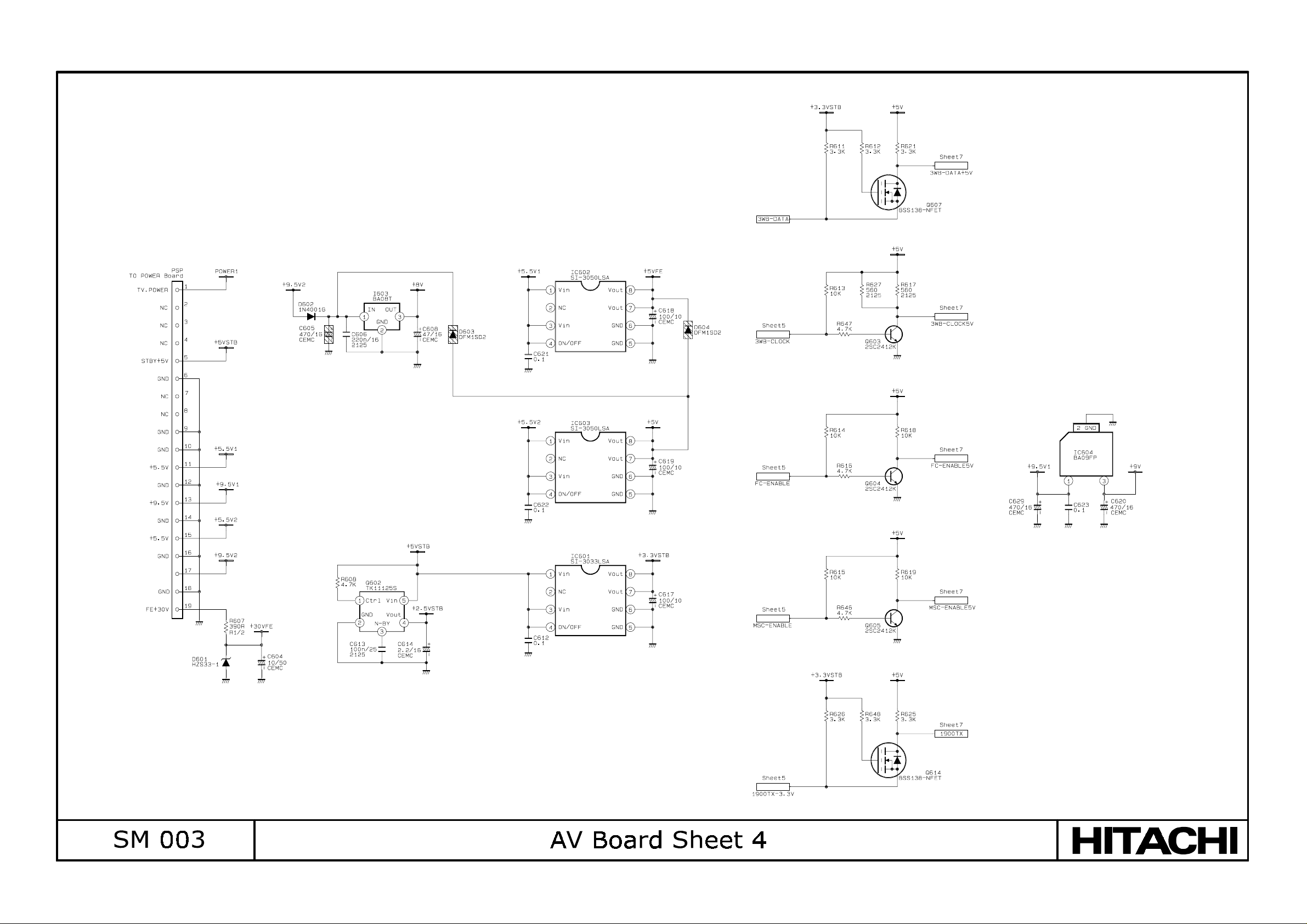
Schematic Page 4 ; Power Circuit (Voltage Regulator) / Level Shifter
Power supply connector PSP from Power Supply board
1 POWER1 Power ON/Stand-by control H;ON, L;Stand-by
2 N.C.
3 N.C.
4 N.C.
5 +5VSTB Stand-by 5V for micro controller circuit
6 GND
7 N.C.
8 N.C.
9 GND
10 GND
11 +5.5V1 5.5V supply 1
12 GND
13 +9.5V1 9.5V supply 1
14 GND
15 +5.5V2 5.5V supply 2
16 GND
17 +9.5V2 9.5V supply2
18 GND
19 FE+30V 30V supply for tuner
Voltage regulators
I603
BA06T Input +9.5V2 - Output +8V
For video chroma circuit (page1)
IC602
SI-3050LSA Input +5.5V1 - Output +5VFE
For tuner (page1)
IC603
SI-3050LSA Input +5.5V2 - Output +5V
For audio processor circuit (page2), comb filter (page6)
IC601
SI-3033LSA Input +5VSTB - Output 3.3VSTB
For micro controller circuit
Q602
TK11125M Input +5VSTB - Output 2.5VSTB
For micro controller circuit
IC604
BA09FP Input +9.5V1 - Output +9V
For interface circuit (page 3)
Level shift for control buses
Q607
Q603
Q604
Q605
Q614
BSS138 3WB-DATA to change from 3V3 to 5V
2SC2412K 3WB-CLOCK to invert with 5V range
2SC2412K FC-ENABLE to invert with 5V range
2SC2412K MSC-ENABLE to invert with 5V range
BSS138 1900TX to change from 3V3 to 5V
27
Page 29

32PD3000 / 42PD3000
Schematic Page 5 ; Micro Controller
IC704
supply voltage ; +3.3VSTB at pin 8, 40, 75 and 92 and +2.5VSTB at pin 6, 22, 56 and 73
control through I
3 wire bus ; 3WB-clock3v3 at pin 41 and 3WB-data3v3 at pin 46
FC-enable at pin 42
MSC-enable at pin 43
OSD enable at pin 44
control through/by AVlink ; output at pin 16 and input at pin 33
RS232C (19200bps); TxD3v3 at pin 32 and RxD3v3 at pin 38
control by I/R in ; at pin 34
X700
IC700
supply voltage ; +3.3VSTB at pin 8
control by I2C ; SDA3v3 at pin 5 and SCL3v3 at pin 6 and WC3v3 at pin 7
IC701
supply voltage ; +3.3VSTB at pin 32
control by address and data buses
IC701B
IC703
supply voltage ; +3.3VSTB at pin 32
control by address and data buses
IC705
supply voltage ; +3.3VSTB at pin 1
SCL3v3 and SDA3v3 are converted for 5V operation in Q700/Q701/Q705/Q706
RGB and BLK are also converted to 5V operation at Q713/Q714/Q715 and IC707
The signal level is also converted between 3V3 in micro and 5V for SCART.
See "micro pins" for micro controller pin functions.
FRONT PANEL BOARD connection PL702
PIN
NO.
Micro controller ; SDA5550
2
C ; SDA3v3 at pin 52 and SCL3v3 at pin 47
6MHz X'tal
EEPROM ; M24C16W (16kbits)
Flash memory for software stored ; AT49LV002N (256Kbytes)
option not fitted.
SRAM ; SMT K6T1008V2E-GB70000 or equivalent (128kbytes)
RESET IC for IC704 ; M62703SL/ML
OSD/TEXT RGB at pin 58/59/60 are syncronized with progressive sync pulses 2H(32KHz)
at pin 32 and V(50/60Hz) at pin 33
AV link is bi-directional bus from pin 10 of SCART101, made by Q709/D701~D703. For the
micro, input and output are separated.
PIN NAME PL702 IN/OUT FUNCTIONS
1 POW LED I Power LED
2 POWER SAVE I POWER2
3 STB+5V I Stand-by 5V power supply
4 GND - GND
5 RM-IN O N.C.
6 A+5V I +5V
7 A/D KEY 2 O Key in 1
8 A/D KEY 1 O Key in 2
9 (BS-LED) - N.C.
10 (MODEM-LED) - N.C.
at Front Control
28
Page 30

32PD3000 / 42PD3000
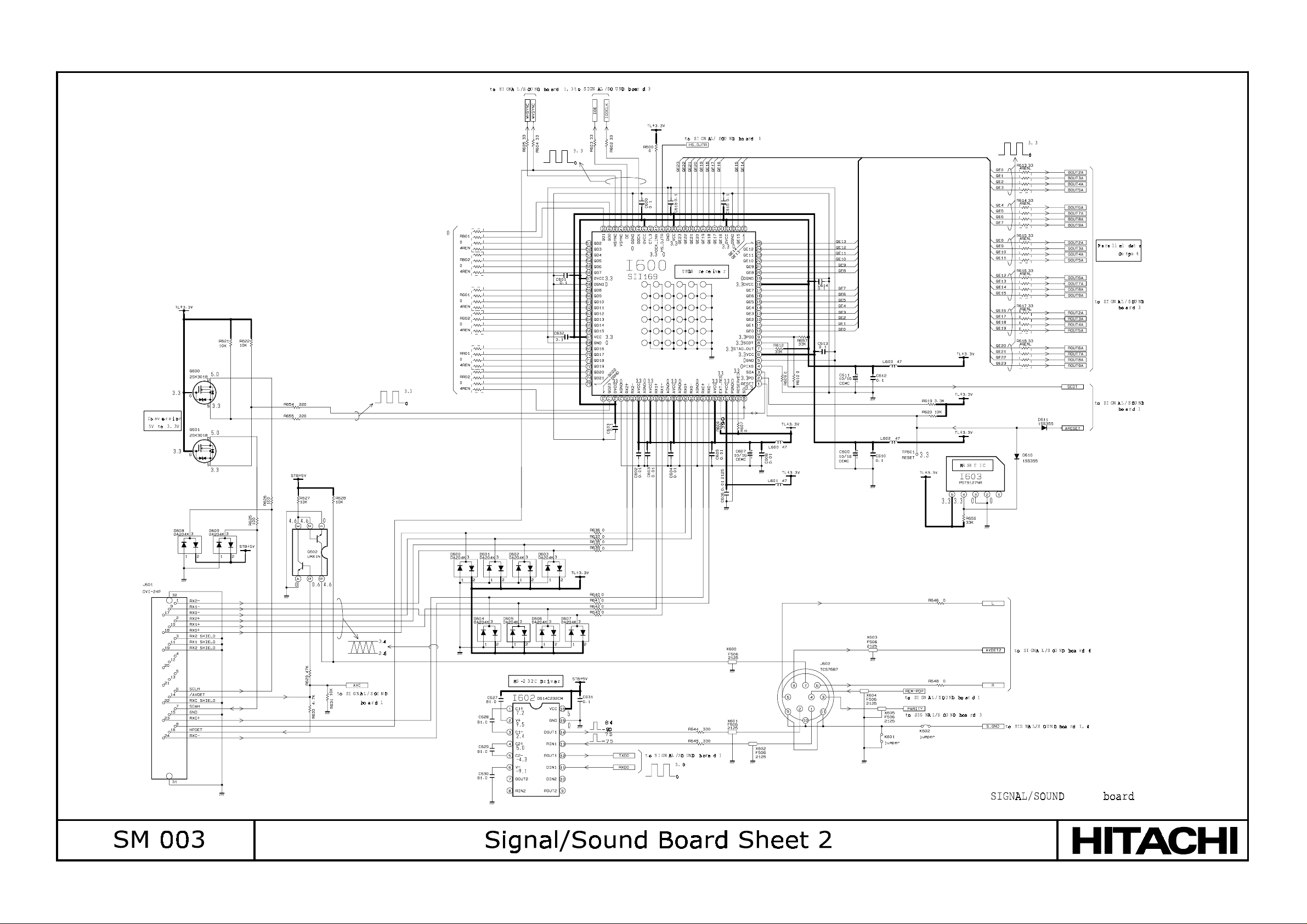
Schematic Page 6 ; COMB Filter / SVHS Output
IC101 COMB filter ; TC9090AF
supply voltage ; +5V at pin 15, 18 and 27
control by I2C ; SDA at pin 8 and SCL at pin 9
CVBS from IC100 pin 26 is filtered by C800/C801/L800/C802 and connected to pin 3
IC101 requires clock at pin 19 supplied from IC100.
SVHS100 SVHS output connector
pin functions
1 GND
2 GND
3 C
4 Y
5 GND(SW)
Y/C separate signals output from IC101 pin 25/23 are also filtered by Q801 base circuit
and Q802 base circuit
Y is amplified to adjust the level at Q119/Q120 for return signal to
IC100 and SVHS Y signal output via buffer Q803
C is amplified to adjust the level at Q121/Q122 for return signal to
IC100 and SVHS C signal output via buffer Q804
29
Page 31

32PD3000 / 42PD3000
Schematic Page 7 ; SCART / FC-MSC Connection
SCART connectors
pin AV1 AV2 AV3 general spec
SCART101 SCART102 SCART100
sound output R sound output R sound output
1
sound input R sound input R sound input
2
sound output L sound output L sound output
3
4 GND GND GND Audio common return
5 GND GND GND Blue return
sound input L sound input L sound input
6
7 N.C. Blue-in Blue-in Blue ; 75ohm, 0.7V+-0.1V
R
R
L
L
Audio output R ; =<1kohm, nominal
0.5Vrms+-3dB, max 2Vrms ; 54% modulation
in FM/AM
Audio input R ; >=10kohm, nominal 0.5Vrms,
min.0.2Vrms, max 2Vrms
Audio output L ; =<1kohm, nominal
0.5Vrms+-3dB, max 2Vrms ; 54% modulation
in FM/AM
Audio input L ; >=10kohm, nominal 0.5Vrms,
min.0.2Vrms, max 2Vrms
Function switch ; >=10kohm, =<2nF, Level 0 ;
8 switch switch switch
9 GND GND GND Green return
10 AVLINK N.C. N.C. Avlink ; TTL level
11 N.C. Green-in Green-in Green ; 75ohm, 0.7V+-0.1V
12 N.C. N.C. N.C. under consideration
13 GND GND GND Red return
14 GND GND GND Blanking return
15 C in Red-in Red-in
16 N.C.
17 GND GND GND Video output return
18 GND GND GND Video input return
19 TV output
Fast
Blanking
Monitor
output
Fast
Blanking
Monitor
output
0~2V, Level 1A : +4.5V~+7V (16:9), Level 1B
: +9.5V~+12V (4:3)
Red/C ; 75ohm, 0.7V+-0.1V (Red), +-3dB at
1Vpp Y signal (C)
Blanking ; 75ohm, logical 0 (off) : 0~0.4V,
logical 1 : +1~+3V
Video/Y output ; 75ohm, 1Vpp +-3dB (sync
0.3V-3dB, +10dB)
20 CVBS/Y in CVBS in CVBS in
21 GND GND GND Common return and contact 8, 10, 12
Video input ; 75ohm, 1Vpp +-3dB (sync 0.3V3dB, +10dB)
Page 32

32PD3000 / 42PD3000
PL700
PL701
connection with FC/MSC board 26ways connector
assuming that 1Vpp video signal with 75ohm terminated is input through SCART100 (AV3)
UV are inverted by Q609/Q612/Q610/Q613 to CbCr(U'V') at pin 25/24 and
those are adjusted to the level at 1.4Vpp
Y is amplified by Q608/Q611 to adjust the level at 1.4V for signal and 0.6V
for sync (2Vpp in total) at pin 26
sound level L and R at pin 6/4 should be 500mVrms on the condition that -
500mVrms audio is input through SCART100(AV3)
BG FM sound with 54% modulation is received
connection with FC/MSC board 26 ways connector
31
Page 33

32PD3000 / 42PD3000
Schematic; AVC Power Supply
I901
switching regulator - controller and power MOS FET ; STR-F6668B
supply voltage at pin 4 ; over +16V (start operating)
pin 1 feedback input
pin 2 Source of power MOS FET
pin 3 Drain of power MOS FET
pin 4 power supply input for controller
pin 5 GND
H901
DC+5V switching regulator module ; uPM0518SA
supply voltage ; DC +120+375V at pin 1
input pin 1 DC(+) voltage input
pin 5 DC(-) voltage input
pin 7 feedback input-1
pin 8 feedback input-2
output pin 6 DC(-) voltage output
pin 9 DC(+) voltage output
I902
photocoupler ; TLP621
I930
switching regulator ; SPI-8010A
supply voltage ; DC +8.5+50V at pin 11
input pin 11 DC voltage input
pin 15 feedback input
output pin 7 switching output
I931
switching regulator ; SI-8010GL
supply voltage ; DC +8+50V at pin 5
input pin 5 DC voltage input
pin 8 feedback input
pin 2 output ON/OFF
output pin 4 switching output
I932
DC+5V series regulator ; SI-3050LSA
supply voltage ; DC +5.1+8V at pin 1,3
input pin 1,3 DC voltage input
output pin 7,8 DC +5V output
I933
switching regulator ; SI-8033JD
supply voltage ; DC +5.3+40V at pin 1
input pin 1 DC voltage input
pin 4 feedback input
pin 5 output ON/OFF
output pin 2 switching output
PSP
connector for AV P.W.B.
PFP1
connector for FC4 unit
PFP2
connector for FC4 unit
32
Page 34

Schematic Drawings
32PD3000 / 42PD3000
33
Page 35

32PD3000 / 42PD3000
34
Page 36

32PD3000 / 42PD3000
35
Page 37
32PD3000 / 42PD3000
36
Page 38

32PD3000 / 42PD3000
37
Page 39

32PD3000 / 42PD3000
38
Page 40

32PD3000 / 42PD3000
39
Page 41

32PD3000 / 42PD3000
40
Page 42

32PD3000 / 42PD3000
41
Page 43

32PD3000 / 42PD3000
42
Page 44
32PD3000 / 42PD3000
43
Page 45

32PD3000 / 42PD3000
44
Page 46

32PD3000 / 42PD3000
45
Page 47

32PD3000 / 42PD3000
46
Page 48

Circuit Boards
32PD3000 / 42PD3000
47
Page 49

32PD3000 / 42PD3000
48
Page 50

AV Power Side A
32PD3000 / 42PD3000
49
Page 51

32PD3000 / 42PD3000
AV Power Side B
50
Page 52

MonitorblockSIGNAL/SOUNDboard[side-A] SIGNAL/SOUNDboardis4layered. Theinnerlayerisnotrecorded.
LKJIHGFEDCBA
6
5
4
3
2
1
6
5
4
3
2
1
LKJIHGFEDCBA
Main chip component location search chart
Cir.No. Position Cir.No. Position Cir.No. Position Cir.No. Position Cir.No. Position Cir.No. Position Cir.No. Position
D003 C4 D602 F1 I003 C4 L600 D2 Q201 D4 QP01 E5 X604 G1
D401 K4 D603 F1 I201 D5 L601 E2 Q202 D4 QS04 A2 X605 F1
D402 K3 D604 E1 I202 B5 L602 E2 Q203 C6 TP001 D3 XS01 A2
D403 K3 D605 E1 I600 E2 L603 E3 Q204 C6 TP002 C4 XS02 B1
D404 K4 D606 F1 I601 G2 L604 G3 Q401 I4 TP601 D2 XS03 B1
D405 J4 D607 E1 I602 G3 LP02 F4 Q402 J4 X001 G5
D406 J2 D610 D2 I603 D1 LP04 E5 Q403 J3 X002 D3
D408 J2 D611 D2 IC401 H2 PDA1 H6 Q404 K1 X201 B5
D409 I3 DP01 F5 IC402 J2 PDS A5 Q405 K1 X202 B5
D410 I1 DS01 A2 IC403 J1 PSC2 G6 Q406 I3 X203 B5
D413 H4 DS02 A2 IP02 F5 Q001 C4 Q407 H4 X204 C4
D414 K2 DS03 A3 L201 B5 Q002 C2 Q408 J3 X600 G1
D415 I3 DS04 B4 L202 B5 Q003 C2 Q600 F2 X601 G1
D600 E1 I001 C3 L203 D5 Q005 G5 Q601 F2 X602 G1
D601 E1 I002 B3 L204 C5 Q006 G5 Q602 G2 X603 G1
Page 53

MonitorblockSIGNAL/SOUNDboard[side-B] SIGNAL/SOUNDboardis4layered. Theinnerlayerisnotrecorded.
ABCDEFGHIJKL
6
5
4
3
2
1
6
5
4
3
2
1
ABCDEFGHIJKL
Main chip component location search chart
Cir.No. Position
D001 D3
D608 F2
D609 F2
QS01 B4
Page 54

FILTER board
LED board for 32V
LED board for 42V
SPEAKER TERMINAL (R) bord (only 42V)
SPEAKER TERMINAL (L) bord (only 42V)
Page 55

54
Troubleshooting Flow Charts
AV Power - 1
32PD3000 / 42PD3000
Page 56

AV Power - 2
55
32PD3000 / 42PD3000
Page 57

56
AV Power - 3
32PD3000 / 42PD3000
Page 58

AV Circuit
57
32PD3000 / 42PD3000
Page 59

32PD3000 / 42PD3000
Assembly Drawings
Audio / Video
58
Page 60

Wiring for Audio / Video Components
32PD3000 / 42PD3000
Specification
1. This Drawing shows the wire dressing and connectors' connection of
AVC3-E Final Assy.
2. Connectors with wire should be inserted into Plug Pin Posts as
shown on the table below
Connector with wire Plug Pin 1 Plug Pin 2
Name Assy List Board Name Board Name
ESC FINAL ASSY Control Board PSC AV Board PL702
EFP1 FINAL ASSY Power Board PFP1 HCP111 P002P
EFP2 FINAL ASSY Power Board PFP2 HCP111 P003P
ESF FINAL ASSY AV Board PSF HCP111 P001
PSP Power Board Assy AV Board PSP - -
3. Into Plug Pin Post with Lock function, connector housing should be
inserted deeply until it can be locked.
4. Into Plug Pin Post without Lock function, connector housing should be
inserted most deeply.
5. Flexible Flat Cable ESF should be fixed as shown on the drawing below
EFP1, EFP2, ESC and
EARTH should never be
bunched together with ZSC
(Nittoh adhesive tape No.188
L=50mm)
Lead clamper for EFP1, EFP2,
ESC and EARTH should be locked
after fixing EARTH and looped
EFP1, EFP2 and ESC wires.
10 10
150
position and lock
59
Page 61

32PD3000E
42PD3000E
32PD3000E
42PD3000E
32PD3000E Monitor Block
The codes in brackets shown in the wiring diagram express
the name of materials.
The key to the codes and materials is shown on the table below.
Code
PC+ABS
ACRYLONITRILE BUTADIENE STYRENE
PS
Material
POLYCARBONATE+
POLYSTYRENE
SIGNAL Board
AC INLET
FILTER Board
(PS)
LED Board
(PC+ABS)
Colored metal plate
(PS)
Page 62

32PD3000E
42PD3000E
32PD3000E
42PD3000E
42PD3000E Monitor Block
(PC+ABS)
PDP Panel Module
Assembly
The codes in brackets shown in the wiring diagram express
the name of materials.
The key to the codes and materials is shown on the table below.
Code
ABS
PC+ABS
AL
ACRYLONITRILE BUTADIENE STYRENE
ACRYLONITRILE BUTADIENE STYRENE
Material
POLYCARBONATE+
ALUMINUM
POWER UNIT
(ABS)
(PC+ABS)
(PC+
ABS)
(AL)
(PC+ABS)
(PC+
ABS)
SIGNAL/SOUND
Board Assembly
(ABS)
(PC+ABS)
(PC+ABS)
Page 63

32PD3000 / 42PD3000
32 inch Monitor Wiring A
62
Page 64

32 inch Monitor Wiring B
32PD3000 / 42PD3000
63
Page 65

32PD3000 / 42PD3000
42 inch Monitor Wiring A
64
Page 66

32PD3000 / 42PD3000
65
Page 67

32PD3000 / 42PD3000
24 way Digital Interface Cable
Connection
AVC(FC4)
P301P
DV174320-4004
1 TX2-
2 TX2+
3 SHIELD --- SHIELD
4 N.C. --- N.C.
5 N.C. --- N.C.
6 SCLH
7 SDAH
8 N.C. --- N.C.
9 TX1-
10 TX1+
11 SHIELD --- SHIELD
12 N.C. --- N.C.
PDP
TX2-
TX2+
SCLH
SDAH
TX1-
TX1+
AVC(FC4)
P302P
TC57587-01-401
1 TXD
2 RXD
3 PARITY
4 REMO-PDP
5 AUDIO L
6 AUDIO R
7 PDDET
8 AVDET2
PDP
TXD
RXD
PARITY
REMO-PDP
AUDIO L
AUDIO R
PDDET
AVDET2
13 N.C. --- N.C.
14 +5VAVDET
15 GND --- GND
16 HPDET
17 TXD-
18 TXD+
19 SHIELD --- SHIELD
20 N.C. --- N.C.
21 N.C. --- N.C.
22 SHIELD --- SUIELD
23 TXC+
24 TXC-
+5VAVDET
HPDET
TXD-
TXD+
TXC+
TXC-
66
Page 68

Microprocessor Pins
32PD3000 / 42PD3000
Pin
No.
Port 0
0.0 POWER-
9
0.
10
1
0.
11
2
0.
12
3
0.
13
4
0.
14
5
0.6 WC#
15
INVERTED (I)
FUNCTION
ON
POWER1 OUT
POWER2 OUT
(I) PM-RESET OUT PDP reset
EEPROM
OR BUFFERED
(B)
FUNCTION
IN
(I) POWERLED 5V
(I) OSDRESET
OUT
IN/OUT
Power key
input
Power control
1
Power control
2
OUT
OUT PC OSD reset
Power LED
control
EEPROM
enable
H(1.5V)
H(1.0V)
H(1.5V) H(1.5V) H(1.5V)
on
standby
L
L L
power
save
H(1.2V)
0.7 AV-LINK-
16
Port 1
41
42
43
44
45
46
47
52
OUT
1.0 3WBCLOCK
1.1 FCENABLE
1.2 MSCENABLE
1.
(I) OSD-EN OUT
3
1.
(I) MSP-RESET OUT
4
1.5 3WBDATA
1.
SCL-3V3 (B) SCL+5V OUT I2C bus clock
6
1.
SDA-3V3 (B) SDA+5V
7
(I) AV LINK OUT
(I) 3WBCLOCK 5V
(I) FCENABLE 5V
(I) MSCENABLE 5V
(B) 3WBDATA+5V
OUT
OUT FC enable
OUT MSC enable
IN/OUT 3 wire buses
IN/OU
T
AV link
output
3 wire bus
clock
PC OSD
enable
MSP3410
reset
data
I2C bus data
Port 2
2.
24
0
ADC0
FROM
SCART1 PIN 8
IN
Scart 101
(AV1) pin 8
detect
67
Page 69

32PD3000 / 42PD3000
2.
25
1
2.
26
2
2.
27
3
Port 3
3.
31
0
3.1 1900TX-
32
3.
33
2
3.
34
3
3.
35
4
ADC1
PDDET FROM PDP IN
ADC3
IF TRAP
3v3
SCI
IR1 IR FROM PDP IN IR input
FRONTSVHSSOCKET
FROM TUNER
AGC
FROM FRONT
SWITCHES
ADJACENT
CHANNELS
OUT
FROM
AVLINK
IN
IN
IN
OUT Not used
IN AV link input
AGC level
detect
PDP ON
detect
Vol+/&Prog.+/- key
input
PDP
communicatio
n via RS232C
S-VHS socket
detect
3.
36
5
3.
37
6
3.
38
7
Port 4
4.
48
2
4.
49
3
MAP1 A18 ON SRAM OUT
MAP2
1900RX IN
MEM RD# OUT
MEM WR# OUT
A15/A18
SWITCH
OUT
SRAM
mapping
SRAM
mapping
PDP
communicatio
n via RS232C
SRAM output
enable
SRAM write
enable
68
Page 70

Connections to FC4
PSF at AVC P001 at FC4
Pin
PIN NAME PIN NAME IN/OUT FUNCTIONS NOTE
No.
1 GND GND I/O I2C bus DATA
2 N.C. N.C. I/O I2C bus CLOCK
3 GND GND - GND
4 DATA DATA I/O 3 wires DATA 5V CMOS
5 CLK CLK I 3 wires CLOCK 5V CMOS
6 GND GND - GND
7 FC-ENA FC-ENA I FC micro enable 5V CMOS
8 MSC-ENA OSD-CS I MSC micro enable 5V CMOS
9 DATA OSD-DATA I 3 wires DATA 5V CMOS
10 CLK OSD-CLK I 3 wires CLOCK 5V CMOS
32PD3000 / 42PD3000
11 GND GND - GND
12 N.C. N.C.(2H) O 2H sync for OSD
13 N.C. K_DET I
14 N.C. N.C.(2V) O 2V sync for OSD
15 N.C. KMASK I
16 GND GND - GND
RS232C-
17
PDP(TxD)
RS232C-
18
PDP(RxD)
19 GND GND - GND
20 +5VSTB AVDET I PDP control
21 N.C. N.C. I MATRIX control
22 Remo-PDP Remo-PDP O
23 GND N.C. - GND
32C-PDP (TXD) I RS232C-TxD 5V CMOS
32C-PDP (RXD) O RS232C-RxD 5V CMOS
Enable for OSD
generator
RESET for OSD
generator
R/C command from
PDP
5V CMOS
24 PM RST PM RST I PDP control 5V CMOS
25 PD DET PD DET O PDP control 5V CMOS
26 GND GND - GND
27 MY MY I Video Y 1.4V±0.06Vp-p
28 MCb MCb I Video Cb 0.7v±0.03Vp-p
29 MCr MCr I Video Cr 0.7v±0.03Vp-p
69
Page 71

32PD3000 / 42PD3000
30 GND GND - GND
31 MH MH I Main H sync 5V CMOS
32 MV MV I Main V sync 5V CMOS
33 GND GND - GND
34 SY SY I Sub Y/G
35 SCb SCb I Sub Cb/B 0.7v±0.03Vp-p
36 SCr SCr I Sub Cr/R 0.7v±0.03Vp-p
37 GND GND - GND
38 SH SH I Sub H sync 5V CMOS
39 SV SV I Sub V sync 5V CMOS
40 GND GND - GND
41 GND
42 GND
43 GND
44 GND
45 GND GND(OSD/Ym) I GND
46 GND GND - GND
GND(OSD/TXT
G)
GND(OSD/TXT
B)
GND(OSD/TXT
R)
GND(OSD
BLK/Ys)
I GND
I GND
I GND
I GND
1.4V±0.06Vp-p (Y) /
0.7Vpp±0.03Vpp (G)
47 AUDIO L AUDIO L I Audio L typ 500mVrms
48 GND GND - GND
49 AUDIO R AUDIO R I Audio R typ 500mVrms
50 GND GND - GND
P002P at FC4
PIN
PIN NAME IN/OUT FUNCTIONS NOTE
NO.
1 FA+6.0V I 6V power supply 460mA
2 FA+6.0V I 6V power supply
3 GND - GND
4 GND - GND
5 FSTB+5V I Stand-by +5V 50mA
6 FSTB+5V I Stand-by +5V
7 GND - GND
70
Page 72

P003P at FC4
PIN
PIN NAME IN/OUT FUNCTIONS NOTE
NO.
1 D+1.8V I 1.8V power supply 500mA
2 D+1.8V I 1.8V power supply
3 GND - GND
4 GND - GND
5 D+3.3V I 3.3V power supply 350mA
6 D+3.3V I 3.3V power supply
7 D+3.3V I 3.3V power supply
8 GND - GND
9 GND - GND
32PD3000 / 42PD3000
71
Page 73

32PD3000 / 42PD3000
PCB Connectors
AVC
FINA
ESC 2908877
EFP
EF22161
1
EFP
EF22171
2
ESF EK01108
ED04153
PSP
U
L
CO-10C-C2R0-431
ASS
Y
FINA
L
CO-07C-C1R5-
ASS
391-ZH
Y
FINA
L
CO-09C-C1R5-
ASS
391-ZH
Y
FINA
L
PRW-SML2CD50P-L700
ASS
Y
Powe
CP-
r
19BP1R2VU1.25F
Boar
JN
d
FC4
P001 EA01561R CPC50FP0R5HT-FLZX PSF AV Board
P002P EA01266R CPC07BP1R5HT-SM3A PFP1 Power Board
P003P EA01268R CPC09BP1R5HT-SM3A PFP2 Power Board
P301P EY01501 PJX-DVI(F)24P RA SOK PDP Signal Audio Board
P302P EY01491 PJX-YKF51-5376 PDP Signal Audio Board
P501P EA01247R CPC08BP1R5VT-SM3 For Alignment
P601P EY01062 PJX-DSUB JACK PC Input Terminal
AV Board
PSF EA00932R CPC50FP0R5VT-FH12 P001 FC4
PSP ED04163U CP-19BS1R2VU1.25FJN PSP PowerBoard
PL702 EA00349R CPC10PH2R0VTPH-SM3 PSC ControlBoard
Power Control Board
PFP1 EA01246R CPC07BP1R5VT-SM3 P002P FC4
PFP2 EA01248R CPC09BP1R5VT-SM3 P003P FC4
PSC EA00069R CPC10PH2R0HTPH-SM3 PL702 AV Board
Contr
ol
Board
Power
Board
Power
Board
AV
Board
AV
Board
EA00069R CPC10PH2R0HTP
PSC
PFP1 EA01246R CPC07BP1R5VT-
PFP2 EA01248R CPC09BP1R5VT-
EA00932R CPC50FP0R5VT-
PSF
ED04163
PSP
U
H-SM3
SM3
SM3
FH12
CP19BS1R2VU1.25F
JN
AV
PL702 EA00349R CPC10PH2R0VTP
Boar
d
P002P EA01266R CPC07BP1R5HT-
FC4
P003P EA01268R CPC09BP1R5HT-
FC4
FC4 P001
- - - -
EA01561R CPC50FP0R5HT-
H-SM3
SM3A
SM3A
FLZX
72
Page 74

Replacement Parts
Signal / Sound Board
CIR No. DESCRIPTION ECN#[040] Part No.
# PSA PT3 SIGNAL/AUDIO JP06091
# "PSA PT3 SIGNAL/AUDIO FOR ""42" JP06092
# PSA PT3 SIGNAL/AUDIO JP06093
# PSA PT3 SIGNAL/AUDIO JP06094
B PWB PT3 SIGNAL/AUDIO JA04554
CP01 470UF 25V ALUMINIUM ELECTROLYTIC CAPACITOR
AL01857R
CP02 1000UF 6.3V ALUMINIUM ELECTROLYTIC
CAPACITOR AL01833R
CP04 CCC106M06-B-20CT (10UF 6.3V 2012M) AA00968R
CP05 CEC101M06-EWCT AD00416R
CP09 CEC101M06-EWCT AD00416R
CP10 CEC101M06-EWCT AD00416R
CS02 CEC100M16-EWCT AD00436R
CS03 CAP2125CHIP 10000PFKB 50V TAPE 0893044R
CS04 CEC101M16-EWCT AD00441R
CS07 CCC333K50-B-16CT AA01814R
CS10 CCC106M06-B-20CT (10UF 6.3V 2012M) AA00968R
C001 CAP 1608CHIP 10PFCCH 50V TAPE 0893113R
C002 CAP 1608CHIP 10PFCCH 50V TAPE 0893113R
C003 CCC103K50-B-16CT MCH18 AA01802R
C004 CERAMIC CAPACITOR(1.0U F 6.3V) AA01111R
C005 CCC103K50-B-16CT MCH18 AA01802R
C008 CCC103K50-B-16CT MCH18 AA01802R
C010 CCC103K50-B-16CT MCH18 AA01802R
C011 CCC103K50-B-16CT MCH18 AA01802R
C012 CERAMIC CAPACITOR(1.0U F 6.3V) AA01111R
C203 CERAMIC CAPACITOR(1.0U F 6.3V) AA01111R
C204 CERAMIC CAPACITOR(1.0U F 6.3V) AA01111R
C205 CERAMIC CAPACITOR(1.0U F 6.3V) AA01111R
C206 CERAMIC CAPACITOR(1.0U F 6.3V) AA01111R
C207 CERAMIC CAPACITOR(1.0U F 6.3V) AA01111R
C210 CERAMIC CAPACITOR(1.0U F 6.3V) AA01111R
C211 CEC101M06-EWCT AD00416R
C401 CAP 1608CHIP 470PFJCH 50V TAPE 0893135R
C402 CAP 1608CHIP 470PFJCH 50V TAPE 0893135R
C403 CEC4R7M25-EWCT AD00447R
C404 CEC4R7M25-EWCT AD00447R
C405 CAP 1608CHIP 1500PFKB 50V TAPE 0893211R
C406 CAP 1608CHIP 1500PFKB 50V TAPE 0893211R
C407 CERAMIC CAPACITOR(0.47UF 10V) AA01121R
C408 CERAMIC CAPACITOR(0.47UF 10V) AA01121R
C409 CEC4R7M50-EWCT AD00478R
C410 CEC4R7M50-EWCT AD00478R
C411 CERAMIC CAPACITOR(1.0U F 6.3V) AA01111R
C412 CCC333K50-B-16CT AA01814R
C413 CEC4R7M25-EWCT AD00447R
C414 CEC4R7M25-EWCT AD00447R
C415 CAP 1608CHIP 180PFJCH 50V TAPE 0893129R
C416 CAP 1608CHIP 180PFJCH 50V TAPE 0893129R
C417 CAP.-ELECTRO. 330UF-M(SMG) 16V 0800344R
C418 CEC4R7M25-EWCT AD00447R
C419 CEC4R7M25-EWCT AD00447R
C420 CEC4R7M25-EWCT AD00447R
C421 CCC333K50-B-16CT AA01814R
C422 CCC333K50-B-16CT AA01814R
C423 CCC333K50-B-16CT AA01814R
C424 CCC333K50-B-16CT AA01814R
C425 CCC333K50-B-16CT AA01814R
C426 CCC333K50-B-16CT AA01814R
C427 CCC333K50-B-16CT AA01814R
C428 CCC103K50-B-16CT MCH18 AA01802R
C429 CEC010M50-EWCT AD00475R
C430 CEC100M16-EWCT AD00436R
C431 CEC100M16-EWCT AD00436R
C432 CAP.-ELECTRO. 330UF-M(SMG) 16V 0800344R
C435 CEC100M16-EWCT AD00436R
C436 CEC4R7M50-EWCT AD00478R
C437 CEC4R7M50-EWCT AD00478R
C438 CAP 1608CHIP 120PFJCH 50V TAPE 0893127R
C439 CAP 1608CHIP 120PFJCH 50V TAPE 0893127R
C440 CAP.-POLYESTER 1.0U F-J 50V 0880207R
C441 CAP.-POLYESTER 1.0U F-J 50V 0880207R
C442 CAP.-POLYESTER 1.0U F-J 50V 0880207R
C443 CAP.-POLYESTER 1.0U F-J 50V 0880207R
C444 CAP.-POLYESTER FILM 0.22UF-K 50V 0880018R
C445 CAP.-POLYESTER FILM 0.22UF-K 50V 0880018R
C446 CEC100M16-EWCT AD00436R
C447 CEC100M16-EWCT AD00436R
C452 CCC333K50-B-16CT AA01814R
32PD3000 / 42PD3000
C453 CCC333K50-B-16CT AA01814R
C454 CEC010M50-EWCT AD00475R
C455 CCC333K50-B-16CT AA01814R
C456 CCC333K50-B-16CT AA01814R
C457 CCC333K50-B-16CT AA01814R
C458 CEC010M50-EWCT AD00475R
C459 CCC333K50-B-16CT AA01814R
C460 CCC333K50-B-16CT AA01814R
C461 CAP.-ELECTRO.470UF-M 16V 0800353R
C462 CAP.-ELECTRO.470UF-M 16V 0800353R
C463 CEC470M16-EWCT AD00439R
C464 CCC333K50-B-16CT AA01814R
C467 CAP.-ELECTRO 1000UF 16V 0800361N
C468 CERAMIC CAPACITOR(1UF 10V-F) AA01101R
C469 CAP 1608CHIP 1500PFKB 50V TAPE 0893211R
C470 CAP 1608CHIP 1500PFKB 50V TAPE 0893211R
C473 2200UF 10V ALUMINIUM ELECTROLYTIC
CAPACITOR AL01843R
C474 2200UF 10V ALUMINIUM ELECTROLYTIC
CAPACITOR AL01843R
C475 2200UF 10V ALUMINIUM ELECTROLYTIC
CAPACITOR AL01843R
C476 2200UF 10V ALUMINIUM ELECTROLYTIC
CAPACITOR AL01843R
C482 CAP.-POLYESTER 0.01U F-K 50V 0880009R
C600 CCC333K50-B-16CT AA01814R
C601 CCC333K50-B-16CT AA01814R
C602 CCC103K50-B-16CT MCH18 AA01802R
C603 CCC103K50-B-16CT MCH18 AA01802R
C604 CCC103K50-B-16CT MCH18 AA01802R
C605 CCC103K50-B-16CT MCH18 AA01802R
C606 CAP2125CHIP 10000PFKB 50V TAPE 0893044R
C607 CEC100M16-EWCT AD00436R
C608 CCC103K50-B-16CT MCH18 AA01802R
C609 CEC100M16-EWCT AD00436R
C610 CCC333K50-B-16CT AA01814R
C611 CEC100M16-EWCT AD00436R
C612 CCC333K50-B-16CT AA01814R
C613 CCC333K50-B-16CT AA01814R
C614 CCC333K50-B-16CT AA01814R
C615 CCC333K50-B-16CT AA01814R
C616 CCC333K50-B-16CT AA01814R
C627 CERAMIC CAPACITOR(1.0U F 6.3V) AA01111R
C628 CERAMIC CAPACITOR(1.0U F 6.3V) AA01111R
C629 CERAMIC CAPACITOR(1.0U F 6.3V) AA01111R
C630 CERAMIC CAPACITOR(1.0U F 6.3V) AA01111R
C631 CCC333K50-B-16CT AA01814R
C632 CCC333K50-B-16CT AA01814R
C633 CCC333K50-B-16CT AA01814R
DP01 DIODE SFPJ-73 CC01661R
DS01 DIODE.CHIP 1SS355 CC00003R
DS02 DIODE.CHIP 1SS355 CC00003R
DS04 CHIP DIODE RD5.1UM(B2-T) CC00142R
D001 DIO-1S2835(T2B) 2333121R
D003 DIODE.CHIP 1SS355 CC00003R
D401 DIODE.CHIP RB491D (20V) CC00632R
D402 DIODE.CHIP RB491D (20V) CC00632R
D403 DIODE.CHIP RB491D (20V) CC00632R
D404 DIODE.CHIP RB491D (20V) CC00632R
D405 DIODE.CHIP 1SS355 CC00003R
D406 DIODE.CHIP 1SS355 CC00003R
D407 DIODE AM01Z (200 TAPE) 1A 2339491M
D408 DIODE.CHIP 1SS355 CC00003R
D409 DIODE.CHIP 1SS355 CC00003R
D410 ZENER.CHIP UDZ 7.5B CC00826R
D413 ZENER.CHIP UDZ 5.1B CC00822R
D414 ZENER.CHIP UDZ 5.1B CC00822R
D600 DIODE CHIP DA204K-TPTX CC10721R
D601 DIODE CHIP DA204K-TPTX CC10721R
D602 DIODE CHIP DA204K-TPTX CC10721R
D603 DIODE CHIP DA204K-TPTX CC10721R
D604 DIODE CHIP DA204K-TPTX CC10721R
D605 DIODE CHIP DA204K-TPTX CC10721R
D606 DIODE CHIP DA204K-TPTX CC10721R
D607 DIODE CHIP DA204K-TPTX CC10721R
D608 DIODE CHIP DA204K-TPTX CC10721R
D609 DIODE CHIP DA204K-TPTX CC10721R
D610 DIODE.CHIP 1SS355 CC00003R
D611 DIODE.CHIP 1SS355 CC00003R
IC401 IC NJW1138M CK36481R
IC402 NJM2192AM CK35311R
IC403 ANALOG MONOLITHIC IC BU4052BCF-E2
CK31991R
73
Page 75

32PD3000 / 42PD3000
IC404 DIGITAL POWER IC(TA2020-020) CP07681U
IP02 MONO IC SI-8033JD CK37162R
IS01 ANALOG MONOLITHIC IC (BA6956AN) CP08241U
I001 DIGITAL MONOLITHIC IC (HD64F3397) CK06571U
I002 DIGITAL MONOLITHIC IC (M24C16-WMN6T)
CK32542R
I003 DIGITAL MONOLITHIC IC (PST9142-T(FP)) CK06091R
I201 DIGITAL MONOLITHIC IC (HD74LVC244AT) CK32661R
I202 DIGITAL MONOLITHIC IC (THC63LVDM83R)
CK32072R
I600 DIGITAL MONOLITHIC IC (SII169) CK37891U
I602 DIGITAL MONOLITHIC IC (DS14C232CM) CK04681R
I603 ANALOG MONOLITHIC IC(PST9127NR) CK06097R
JSW 1.5MM PITCH 13P FG CONNECTOR SOCKET ED04241
J401 JAK-YKC21-1P-BLK 2672967
J601 CONNECTOR ED0347 3
J602 SOCKET YKF51-5376 EY01491
KP04 0.60MM TAPED JUMP.WIRE 2784381M
K208 CHIP RESISTOR RECJUMPER-1-16C16T1608 0790001R
K209 CHIP RESISTOR RECJUMPER-1-16C16T1608 0790001R
K210 CHIP RESISTOR RECJUMPER-1-16C16T1608 0790001R
K211 0.60MM TAPED JUMP.WIRE 2784381M
K401 0.60MM TAPED JUMP.WIRE 2784381M
K404 0.60MM TAPED JUMP.WIRE 2784381M
K406 0.60MM TAPED JUMP.WIRE 2784381M
K407 0.60MM TAPED JUMP.WIRE 2784381M
K408 0.60MM TAPED JUMP.WIRE 2784381M
K409 0.60MM TAPED JUMP.WIRE 2784381M
K417 0.60MM TAPED JUMP.WIRE 2784381M
K418 0.60MM TAPED JUMP.WIRE 2784381M
K419 0.60MM TAPED JUMP.WIRE 2784381M
K420 0.60MM TAPED JUMP.WIRE 2784381M
K421 0.60MM TAPED JUMP.WIRE 2784381M
K473 0.60MM TAPED JUMP.WIRE 2784381M
K474 0.60MM TAPED JUMP.WIRE 2784381M
K475 0.60MM TAPED JUMP.WIRE 2784381M
K476 0.60MM TAPED JUMP.WIRE 2784381M
K480 0.60MM TAPED JUMP.WIRE 2784381M
K601 0.60MM TAPED JUMP.WIRE 2784381M
K602 0.60MM TAPED JUMP.WIRE 2784381M
LP02 C12-K4.5L SMD COIL 100UH BA00632R
LP03 FILT.COIL(LHL08 47UH) 2125806N
LP04 3225 CHIP COIL 47UH BA00712R
LS01 FILT.COIL(LHL08 47UH) 2125806N
LS02 COIL FERRITE BEAD BL02RN1-R62T4 BZ01421R
L201 3225 CHIP COIL 47UH BA00712R
L202 3225 CHIP COIL 47UH BA00712R
L203 3225 CHIP COIL 47UH BA00712R
L204 3225 CHIP COIL 47UH BA00712R
L401 COIL 10UH 2.1A BH01811R
L402 COIL 10UH 2.1A BH01811R
L403 COIL 10UH 2.1A BH01811R
L404 COIL 10UH 2.1A BH01811R
L409 COIL FERRITE BEAD BL02RN1-R62T4 BZ01421R
L410 COIL FERRITE BEAD BL02RN1-R62T4 BZ01421R
L413 COIL FERRITE BEAD BL02RN1-R62T4 BZ01421R
L414 COIL FERRITE BEAD BL02RN1-R62T4 BZ01421R
L415 DC COM. MODE CHOKE COIL 7UH 2A BZ05521
L416 DC COM. MODE CHOKE COIL 7UH 2A BZ05521
L600 3225 CHIP COIL 47UH BA00712R
L601 3225 CHIP COIL 47UH BA00712R
L602 3225 CHIP COIL 47UH BA00712R
L603 3225 CHIP COIL 47UH BA00712R
N401 SOUND HEATSINK 3000 MA01474
N403 M3X10 SCREW WITH WASHER 4520889
PAS1 PLUG PIN SUB MINI 2P 2902261
PAS2 PLUG 03P EH TAPE 2902262R
PDA1 1.5MM PITCH 12P CONNECTOR BASE SM3 EA01252R
PDS CONNECTOR DF13-20DP-1.25V( 59) EA01092R
PG2 PLUG 02BP3R9V-VH(PBT) ED01531
PMW PLUG 07P EH TAPE 2902266R
PPA PLUG 04P EH TAPE 2902263R
PPS PLUG PIN SUB MINI 9P 2902268
PSC2 CONNECTOR CPC06PH2R0VTPH-SM3 EA00345R
PSU 5P XH CONNECTOR PLUG B 5B-XH-A ED03494
QS01 TRS 2SA1576-T107-R 2316231R
QS04 TRS.CHIP DTC144EE TL CA00983R
Q001 TRS.CHIP 2SC4617 TL (R/S) 1323293R
Q005 TRS.CHIP 2SA1774 TL (R/S) 1323294R
Q006 TRS.CHIP 2SA1774 TL (R/S) 1323294R
Q201 TRS.CHIP 2SC4617 TL (R/S) 1323293R
Q202 TRS.CHIP DTC114EE TL CA00981R
Q203 TRS.CHIP 2SK3018 CA01011R
Q204 TRS.CHIP 2SK3018 CA01011R
Q401 TRS.CHIP 2SC4617 TL (R/S) 1323293R
Q402 TRS.CHIP 2SC4617 TL (R/S) 1323293R
Q403 TRS.CHIP DTC114EE TL CA00981R
Q404 TRS.CHIP DTC323TK CA00771R
Q405 TRS.CHIP DTC323TK CA00771R
Q406 TRS.CHIP DTC114EE TL CA00981R
Q407 TRS.CHIP DTC323TK CA00771R
Q408 TRS.CHIP DTC114EE TL CA00981R
Q600 TRS.CHIP 2SK3018 CA01011R
Q601 TRS.CHIP 2SK3018 CA01011R
Q602 TRS.CHIP UMX1N 1323392
RB01 RES.CHIP 1/16W 0 OHM AQ00001R
RB02 RES.CHIP 1/16W 0 OHM AQ00001R
RG01 RES.CHIP 1/16W 0 OHM AQ00001R
RG02 RES.CHIP 1/16W 0 OHM AQ00001R
RP09 CHIP RESISTOR RECJUMPER-1-16C16T1608 0790001R
RR01 RES.CHIP 1/16W 0 OHM AQ00001R
RR02 RES.CHIP 1/16W 0 OHM AQ00001R
RS01 RES.CHIP 1/16W 82K OHM 0790063R
RS02 RES.CHIP 1/16W 27K OHM 0790056R
RS03 RES.CHIP 1/16W 100 OHM 0790024R
RS04 RES.CHIP 1/16W 100 OHM 0790024R
RS05 RES.CHIP 1/16W 10K OHM 0790051R
RS06 CHIP RESISTOR RECJUMPER-1-16C16T1608 0790001R
RS06 RES.CHIP 1/16W 1.0M OHM 0790077R
RS07 RES.MTL FLM 1W 5.6 OHM AT01049S
RS08 ES.-CARBON FLM 1/2W 1.5-J 0188093M
RS09 RES.CHIP 1/16W 10K OHM 0790051R
RS10 RES.CHIP 1/16W 10K OHM 0790051R
RS11 RES.CHIP 1/16W 10K OHM 0790051R
RS14 RES.CHIP 1/16W 10K OHM 0790051R
RS15 RES.CHIP 1/16W 1.0K OHM 0790037R
RY401 RELAY DQ1SU FJ00291
RY402 RELAY DQ1SU FJ00291
R0A1 CHIP RESISTOR RECJUMPER-1-16C16T1608 0790001R
R0A6 CHIP RESISTOR RECJUMPER-1-16C16T1608 0790001R
R0A8 RES.CHIP 1/16W 100 OHM 0790024R
R0A9 RES.CHIP 1/16W 10K OHM 0790051R
R0C7 RES.CHIP 1/16W 10K OHM 0790051R
R0C8 CHIP RESISTOR RECJUMPER-1-16C16T1608 0790001R
R0C9 RES.CHIP 1/16W 3.9K OHM 0790045R
R0E2 CHIP RESISTOR RECJUMPER-1-16C16T1608 0790001R
R0E3 CHIP RESISTOR RECJUMPER-1-16C16T1608 0790001R
R0E4 CHIP RESISTOR RECJUMPER-1-16C16T1608 0790001R
R0E5 CHIP RESISTOR RECJUMPER-1-16C16T1608 0790001R
R0E8 RES.CHIP 1/16W 10K OHM 0790051R
R001 CHIP RESISTOR RECJUMPER-1-16C16T1608 0790001R
R002 CHIP RESISTOR RECJUMPER-1-16C16T1608 0790001R
R004 RES.CHIP 1/16W 100 OHM 0790024R
R005 CHIP RESISTOR RECJUMPER-1-16C16T1608 0790001R
R005 RES.CHIP 1/16W 100 OHM 0790024R
R006 RES.CHIP 1/16W 100 OHM 0790024R
R007 RES.CHIP 1/16W 100 OHM 0790024R
R008 RES.CHIP 1/16W 1.0K OHM 0790037R
R009 RES.CHIP 1/16W 1.0K OHM 0790037R
R014 RES.CHIP 1/16W 4.7K OHM 0790046R
R015 RES.CHIP 1/16W 4.7K OHM 0790046R
R016 CHIP RESISTOR RECJUMPER-1-16C16T1608 0790001R
R017 CHIP RESISTOR RECJUMPER-1-16C16T1608 0790001R
R018 CHIP RESISTOR RECJUMPER-1-16C16T1608 0790001R
R019 CHIP RESISTOR RECJUMPER-1-16C16T1608 0790001R
R020 CHIP RESISTOR RECJUMPER-1-16C16T1608 0790001R
R022 RES.CHIP 1/16W 100 OHM 0790024R
R023 RES.CHIP 1/16W 100 OHM 0790024R
R024 CHIP RESISTOR RECJUMPER-1-16C16T1608 0790001R
R025 RES.CHIP 1/16W 100 OHM 0790024R
R026 RES.CHIP 1/16W 100 OHM 0790024R
R027 RES.CHIP 1/16W 100 OHM (4 R) AQ00024R
R028 RES.CHIP 1/16W 100 OHM (4 R) AQ00024R
R029 RES.CHIP 1/16W 100 OHM (4 R) AQ00024R
R030 RES.CHIP 1/16W 100 OHM (4 R) AQ00024R
R032 RES.CHIP 1/16W 100 OHM 0790024R
R035 RES.CHIP 1/16W 100 OHM 0790024R
R036 RES.CHIP 1/16W 10K OHM 0790051R
R039 RES.CHIP 1/16W 100 OHM (4 R) AQ00024R
R042 RES.CHIP 1/16W 100 OHM 0790024R
R043 RES.CHIP 1/16W 10K OHM 0790051R
R044 RES.CHIP 1/16W 10K OHM 0790051R
R046 CHIP RESISTOR RECJUMPER-1-16C16T1608 0790001R
R047 CHIP RESISTOR RECJUMPER-1-16C16T1608 0790001R
R048 CHIP RESISTOR RECJUMPER-1-16C16T1608 0790001R
R053 RES.CHIP 1/16W 100 OHM (4 R) AQ00024R
R054 RES.CHIP 1/16W 4.7K OHM 0790046R
R055 RES.CHIP 1/16W 4.7K OHM 0790046R
R059 RES.CHIP 1/16W 3.9K OHM 0790045R
R063 CHIP RESISTOR RECJUMPER-1-16C16T1608 0790001R
R064 CHIP RESISTOR RECJUMPER-1-16C16T1608 0790001R
R065 CHIP RESISTOR RECJUMPER-1-16C16T1608 0790001R
74
Page 76

32PD3000 / 42PD3000
R066 RES.CHIP 1/16W 100 OHM 0790024R
R068 RES.CHIP 1/16W 100 OHM 0790024R
R075 CHIP RESISTOR RECJUMPER-1-16C16T1608 0790001R
R076 CHIP RESISTOR RECJUMPER-1-16C16T1608 0790001R
R077 RES.CHIP 1/16W 4.7K OHM 0790046R
R078 RES.CHIP 1/16W 4.7K OHM 0790046R
R079 RES.CHIP 1/16W 33K OHM 0790057R
R080 CHIP RESISTOR RECJUMPER-1-16C16T1608 0790001R
R081 CHIP RESISTOR RECJUMPER-1-16C16T1608 0790001R
R083 RES.CHIP 1/16W 100 OHM 0790024R
R084 RES.CHIP 1/16W 1.0K OHM 0790037R
R085 RES.CHIP 1/16W 100 OHM 0790024R
R087 RES.CHIP 1/16W 220 OHM 0790028R
R092 RES.CHIP 1/16W 2.2K OHM 0790042R
R093 RES.CHIP 1/16W 2.2K OHM 0790042R
R094 RES.CHIP 1/16W 4.7K OHM 0790046R
R095 RES.CHIP 1/16W 4.7K OHM 0790046R
R096 RES.CHIP 1/16W 560 OHM 0790034R
R097 RES.CHIP 1/16W 2.2K OHM 0790042R
R098 RES.CHIP 1/16W 1.0K OHM 0790037R
R099 RES.CHIP 1/16W 1.0K OHM 0790037R
R201 RES.CHIP 1/16W 10K OHM 0790051R
R202 RES.CHIP 1/16W 10K OHM 0790051R
R203 RES.CHIP 1/16W 10K OHM 0790051R
R204 RES.CHIP 1/16W 10K OHM 0790051R
R205 RES.CHIP 1/16W 10K OHM 0790051R
R206 RES.CHIP 1/16W 100 OHM 0790024R
R207 RES.CHIP 1/16W 100 OHM 0790024R
R208 CHIP RESISTOR RECJUMPER-1-16C16T1608 0790001R
R209 RES 2125 CHIP JAMPER WIRE 0195250R
R210 RES 2125 CHIP JAMPER WIRE 0195250R
R212 CHIP RESISTOR RECJUMPER-1-16C16T1608 0790001R
R213 RES.CHIP 1/16W 10K OHM 0790051R
R217 RES.CHIP 1/16W 1.0K OHM 0790037R
R227 RES.CHIP 1/16W 5.6K OHM 0790047R
R229 CHIP RESISTOR RECJUMPER-1-16C16T1608 0790001R
R251 RES.CHIP 1/16W 0 OHM AQ00001R
R252 RES.CHIP 1/16W 0 OHM AQ00001R
R253 RES.CHIP 1/16W 0 OHM AQ00001R
R401 RES.CHIP 1/16W 220 OHM 0790028R
R402 RES.CHIP 1/16W 220 OHM 0790028R
R403 RES.CHIP 1/16W 220K OHM 0790068R
R404 RES.CHIP 1/16W 220K OHM 0790068R
R405 RES.CHIP 1/16W 100 OHM 0790024R
R406 RES.CHIP 1/16W 100 OHM 0790024R
R407 RES.CHIP 1/16W 56K OHM 0790061R
R408 RES.-1608CHIP 1/16W 13K-J TAPE 0196096R
R409 RES.-1608CHIP 1/16W 160K-J TAPE 0196123R
R410 RES 1608 CHIP 1/16W 36KJ TAPE 0196106R
R411 RES.-1608CHIP 1/16W 9.1K-J TAPE 0196091R
R412 RES.-1608CHIP 1/16W 110K-J TAPE 0196119R
R413 RES.CHIP 1/16W 10K OHM 0790051R
R414 RES.-1608CHIP 1/16W 910-J TAPE 0196066R
R414 RES.CHIP 1/16W 820 OHM 0790036R
R415 RES.-1608CHIP 1/16W 910-J TAPE 0196066R
R415 RES.CHIP 1/16W 820 OHM 0790036R
R416 RES.-1608CHIP 1/16W 2.4K-J TAPE 0196077R
R417 RES.CHIP 1/16W 5.6K OHM 0790047R
R418 RES.CHIP 1/16W 1.0K OHM 0790037R
R419 RES.CHIP 1/16W 1.0K OHM 0790037R
R420 RES.CHIP 1/16W 1.0K OHM 0790037R
R421 RES.CHIP 1/16W 6.8K OHM 0790048R
R422 RES.CHIP 1/16W 6.8K OHM 0790048R
R423 RES.CHIP 1/16W 1.0K OHM 0790037R
R424 RES.CHIP 1/16W 1.0K OHM 0790037R
R425 RES.CHIP 1/16W 1.0K OHM 0790037R
R426 RES.CHIP 1/16W 1.0K OHM 0790037R
R427 RES.-1608CHIP 1/16W 16K-J TAPE 0196098R
R428 RES.-1608CHIP 1/16W 16K-J TAPE 0196098R
R429 RES.-1608CHIP 1/16W 43K-J TAPE 0196108R
R430 RES.-1608CHIP 1/16W 43K-J TAPE 0196108R
R431 RESISTOR CARBON FILM SRD1/2P-B 10-J 0113701M
R432 RESISTOR CARBON FILM SRD1/2P-B 10-J 0113701M
R433 RES.CHIP 1/16W 10K OHM 0790051R
R434 RES.CHIP 1/16W 10K OHM 0790051R
R435 RES.CHIP 1/16W 2.2K OHM 0790042R
R436 RES.CHIP 1/16W 100K OHM 0790064R
R437 RES.CHIP 1/16W 100 OHM 0790024R
R438 RES.CHIP 1/16W 47K OHM 0790059R
R439 RES.CHIP 1/16W 8.2K OHM 0790049R
R440 CHIP RESISTOR RECJUMPER-1-16C16T1608 0790001R
R441 CHIP RESISTOR RECJUMPER-1-16C16T1608 0790001R
R442 RES.CHIP 1/16W 12K OHM 0790052R
R443 RES.CHIP 1/16W 4.7K OHM 0790046R
R446 RES.CHIP 1/16W 4.7K OHM 0790046R
R447 RES.CHIP 1/16W 4.7K OHM 0790046R
R448 RES.CHIP 1/16W 3.3K OHM 0790044R
R449 RES.CHIP 1/16W 27K OHM 0790056R
R450 RES.CHIP 1/16W 27K OHM 0790056R
R458 RES.CHIP 1/16W 10K OHM 0790051R
R459 RES.CHIP 1/16W 5.6K OHM 0790047R
R460 RES.CHIP 1/16W 100 OHM 0790024R
R461 RES.CHIP 1/16W 10K OHM 0790051R
R462 CHIP RESISTOR RECJUMPER-1-16C16T1608 0790001R
R463 CHIP RESISTOR RECJUMPER-1-16C16T1608 0790001R
R600 CHIP RESISTOR RECJUMPER-1-16C16T1608 0790001R
R602 RES.CHIP 1/16W 33 OHM 0790017R
R603 RES.CHIP 1/16W 33 OHM 0790017R
R604 RES.CHIP 1/16W 33 OHM 0790017R
R605 RES.CHIP 1/16W 33 OHM 0790017R
R606 RES.CHIP 1/16W 390 OHM 0790032R
R607 CHIP RESISTOR RECJUMPER-1-16C16T1608 0790001R
R609 CHIP RESISTOR RECJUMPER-1-16C16T1608 0790001R
R610 CHIP RESISTOR RECJUMPER-1-16C16T1608 0790001R
R612 RES.CHIP 1/16W 33K OHM 0790057R
R613 RES.CHIP 1/16W 33 OHM (4 R) AQ00017R
R614 RES.CHIP 1/16W 33 OHM (4 R) AQ00017R
R615 RES.CHIP 1/16W 33 OHM (4 R) AQ00017R
R616 RES.CHIP 1/16W 33 OHM (4 R) AQ00017R
R617 RES.CHIP 1/16W 33 OHM (4 R) AQ00017R
R618 RES.CHIP 1/16W 33 OHM (4 R) AQ00017R
R619 RES.CHIP 1/16W 3.3K OHM 0790044R
R620 RES.CHIP 1/16W 10K OHM 0790051R
R621 RES.CHIP 1/16W 10K OHM 0790051R
R622 RES.CHIP 1/16W 10K OHM 0790051R
R625 RES.CHIP 1/16W 100 OHM 0790024R
R626 RES.CHIP 1/16W 100 OHM 0790024R
R627 RES.CHIP 1/16W 10K OHM 0790051R
R628 RES.CHIP 1/16W 10K OHM 0790051R
R629 RES.CHIP 1/16W 47K OHM 0790059R
R630 RES.CHIP 1/16W 4.7K OHM 0790046R
R631 RES.CHIP 1/16W 10K OHM 0790051R
R636 CHIP RESISTOR RECJUMPER-1-16C16T1608 0790001R
R637 CHIP RESISTOR RECJUMPER-1-16C16T1608 0790001R
R638 CHIP RESISTOR RECJUMPER-1-16C16T1608 0790001R
R639 CHIP RESISTOR RECJUMPER-1-16C16T1608 0790001R
R640 CHIP RESISTOR RECJUMPER-1-16C16T1608 0790001R
R641 CHIP RESISTOR RECJUMPER-1-16C16T1608 0790001R
R642 CHIP RESISTOR RECJUMPER-1-16C16T1608 0790001R
R643 CHIP RESISTOR RECJUMPER-1-16C16T1608 0790001R
R644 RES.CHIP 1/16W 330 OHM 0790031R
R645 RES.CHIP 1/16W 330 OHM 0790031R
R646 CHIP RESISTOR RECJUMPER-1-16C16T1608 0790001R
R648 CHIP RESISTOR RECJUMPER-1-16C16T1608 0790001R
R654 RES.CHIP 1/16W 220 OHM 0790028R
R655 RES.CHIP 1/16W 220 OHM 0790028R
R656 RES.CHIP 1/16W 33K OHM 0790057R
R657 RES.CHIP 1/16W 33K OHM 0790057R
S001 TACT SWITCH SKHH 2632971
XS01 SMD LC FILTER MEA3216L50R0 BE00391R
XS02 3218 CHIP LC FILTER BE00412R
XS03 3218 CHIP LC FILTER BE00412R
X001 SMD LC FILTER MEA3216L50R0 BE00391R
X002 OSCILLATOR (SMD-49) BL00291R
X600 CHIP CERAMIC FILTER NFL21SP506X1C3D
BK00191R
X601 CHIP CERAMIC FILTER NFL21SP506X1C3D
BK00191R
X602 CHIP CERAMIC FILTER NFL21SP506X1C3D
BK00191R
X603 CHIP CERAMIC FILTER NFL21SP506X1C3D
BK00191R
X604 CHIP CERAMIC FILTER NFL21SP506X1C3D
BK00191R
X605 CHIP CERAMIC FILTER NFL21SP506X1C3D
BK00191R
Z001 UNDECIDED 0
Z002 UNDECIDED 0
Filter Board
CIR No. DESCRIPTION ECN#[035] P#
# PWB ASS'Y PT3 FILTER JT23651
# "PWA PT3 FILTER(""42"")" JT23652
# PWA PT3 FILTER(42/37) JT23653
# PWA PT3 FILTER JT23654
# PWA PT3 FILTER(JP.42) JT23655
# PWA PT3 FILTER JT23656
# PWA PT3 FILTER(W32-PD1) JT23657
# PWA PT3 FILTER(W37-PDH1/PDT1) JT23658
#01 INLET PWB METAL PT3 NA59591
#02 3*12 SCREW WITH WASHER 4520883
#03 LOCK SPACER ML00702
75
Page 77

32PD3000 / 42PD3000
B001 PWB PT3 FILTER JK08262
C001 CAP.-ELECTRO. 100UF-M(SMG) 6.3V 0800324R
C002 CAP.-CERAMIC 0.01UF-Z F 50V TAPE 0244171R
C901 ACROSS CAPA 0.47UF 250V RE474 AN01447S
C902 ACROSS CAPA 0.47UF 250V RE474 AN01447S
C903 ACROSS CAPA 0.47UF 250V RE474 AN01447S
C904 CAP. CERAMIC CS10-B2GA102KYVS AJ00157R
C905 CAP. CERAMIC CS10-B2GA102KYVS AJ00157R
C906 ACROSS CAPA 0.47UF 250V RE474 AN01447S
D001 LED SPR-54MVW 2343561
EGND CONNECTOR ED01651R
E902 CONNECTOR EF09584
E902 CONNECTOR EF09585
E902 CONNECTOR EF09588
F901 HT FUSE 250V 6.3A 5.2X20MM FN00439
F902 HT FUSE 250V 6.3A 5.2X20MM FN00439
H001 GP1U281Q CZ00641
H001 R/C REC.GP1U281R CZ00833
JA402 JACK SP TERMINAL ER00061
JA403 JACK SP TERMINAL ER00061
J901 PLAG-AC INLET SK-1019 2676371
KL911 0.60MM TAPED JUMP.WIRE 2784381M
KL912 0.60MM TAPED JUMP.WIRE 2784381M
KR001 0.60MM TAPED JUMP.WIRE 2784381M
KR002 0.60MM TAPED JUMP.WIRE 2784381M
K001 0.60MM TAPED JUMP.WIRE 2784381M
K004 0.60MM TAPED JUMP.WIRE 2784381M
K005 0.60MM TAPED JUMP.WIRE 2784381M
K007 0.60MM TAPED JUMP.WIRE 2784381M
K008 0.60MM TAPED JUMP.WIRE 2784381M
K480 0.60MM TAPED JUMP.WIRE 2784381M
K481 0.60MM TAPED JUMP.WIRE 2784381M
K902 0.60MM TAPED JUMP.WIRE 2784381M
K903 0.60MM TAPED JUMP.WIRE 2784381M
K904 0.60MM TAPED JUMP.WIRE 2784381M
K905 0.60MM TAPED JUMP.WIRE 2784381M
K906 0.60MM TAPED JUMP.WIRE 2784381M
K907 0.60MM TAPED JUMP.WIRE 2784381M
K908 0.60MM TAPED JUMP.WIRE 2784381M
K909 0.60MM TAPED JUMP.WIRE 2784381M
K910 0.60MM TAPED JUMP.WIRE 2784381M
K911 0.60MM TAPED JUMP.WIRE 2784381M
K913 0.60MM TAPED JUMP.WIRE 2784381M
K921 0.60MM TAPED JUMP.WIRE 2784381M
K922 0.60MM TAPED JUMP.WIRE 2784381M
K925 0.60MM TAPED JUMP.WIRE 2784381M
L481 DC COM. MODE CHOKE COIL 7UH 2A BZ05521
L482 DC COM. MODE CHOKE COIL 7UH 2A BZ05521
L901 LINE FILTER 1.0MH BZ00571
L902 LINE FILTER 5MH 5A BZ04602
L903 LINE FILTER 1.0MH BZ00571
L911 FERRITE BEADS CORE B 2.3UH 2123462M
ND01 LED SPACER LDT-45B MN03331
NF901 FUSE HOLDER FP00031R
NF902 FUSE HOLDER FP00031R
N001 LED HOLDER A5WS NJ01171
N33 PRINTED MATTER QT37872
N902 PRINTED MATTER QT39133
PAS3 PLUG PIN SUB MINI 2P 2902261
PAS4 PLUG PIN SUB MINI 3P 2902262
PPU1 "6P VH CONNECTOR PLUG #2,4,5 NC" ED02812
PPU2 2P PLUG PIN ED02801
PPU3 2P PLUG PIN ED02801
PSC2 PIN POST (PH 6P) 2675285
PSC2 CONNECTOR-6P(PH) 2959055
PSW 8P VH PLUG PIN ED02811
R001 RES.-CARBON FLM 1/16W 680-JB 0700038M
R002 RES.-CARBON FLM 1/16W 560-JB 0700037M
R003 RES.-CARBON FLM 1/16W 1.0K-JB 0700041M
R901 RES.MTL GRAZD FLM 1/2W 3.3M AT03672M
R902 RES.MTL GRAZD FLM 1/2W 3.3M AT03672M
ZJ901 ADHESIVE TAPE (SCOTCH NO.3 W=9) 9449503
Z101 TERMINAL PIN EYELET EU00211
Z102 TERMINAL PIN EYELET EU00211
Z103 TERMINAL PIN EYELET EU00211
Z104 TERMINAL PIN EYELET EU00211
Z105 TERMINAL PIN EYELET EU00211
Z106 TERMINAL PIN EYELET EU00211
Z107 TERMINAL PIN EYELET EU00211
Z108 TERMINAL PIN EYELET EU00211
Z109 TERMINAL PIN EYELET EU00211
Z110 TERMINAL PIN EYELET EU00211
Z111 TERMINAL PIN EYELET EU00211
Z112 TERMINAL PIN EYELET EU00211
Z113 TERMINAL PIN EYELET EU00211
Z130 TERMINAL PIN EYELET EU00211
Z131 TERMINAL PIN EYELET EU00211
Z202 TERMINAL PIN EYELET EU00212
Z204 TERMINAL PIN EYELET EU00212
Z209 TERMINAL PIN EYELET EU00212
Z211 TERMINAL PIN EYELET EU00212
Z212 TERMINAL PIN EYELET EU00212
Z213 TERMINAL PIN EYELET EU00212
Z214 TERMINAL PIN EYELET EU00212
Z215 TERMINAL PIN EYELET EU00212
Z216 TERMINAL PIN EYELET EU00212
Z218 TERMINAL PIN EYELET EU00212
Z230 TERMINAL PIN EYELET EU00212
Z232 TERMINAL PIN EYELET EU00212
Z234 TERMINAL PIN EYELET EU00212
Z235 TERMINAL PIN EYELET EU00212
Z236 TERMINAL PIN EYELET EU00212
Z237 TERMINAL PIN EYELET EU00212
32PD3000
CIR No. DESCRIPTION ECN#[097] P#
# FINAL ASS'Y W32-M3000 UQ32901
# FINAL ASS'Y 32PD3000E UQ32902
# FINAL ASS'Y 32PD3000E UQ32903
# FINAL ASS'Y PD32-A3000-051/081 UQ32904
# FINAL ASS'Y W32-PD1 UQ32907
#001W W103330
#002W W111112
#003W W151217
#003W W151222
#004W UNDECIDED 0
#005W UNDECIDED 0
#01A BEZEL ASSY 32M3000 QD35261
#01AG BEZEL ASS'Y 32PD1 QD35527
#01B BEZEL ASSY 32A3000 QD35262
#011 BEZEL 32M3000 QD35251
#011G BEZEL PDP32 QD21492
#012 POW SW BUTTON 32M PC05601
#012G POWER BUTTON PDP32 PC04961
#012SV POW SW BUTON(SV) PC05631
#013 LED LENS 32M3000 PH32171
#013G LAMP LENS PDP32 PH30111
#014 90 KNOB SPRING SUS 3332452
#014G 90 KNOB SPRING SUS 3332452
#015G SP NET 32PD1 PH30064
#015L SP NET 32M3000 L PH32162
#015L SP NET 32A3000 R PH32163
#015R SP NET 32M3000 R PH32161
#015R SP NET 32A3000 PH32164
#016 HITACHI BADE W40 PU00781
#016G HITACHI BADGE PDP32 PU00651
#017 3*12 SCREW WITH WASHER 4319361
#017G 3*12 SCREW WITH WASHER 4319361
#018 DECO PANEL 32M3000 PH32151
#018C DECO PANEL 32A3000 PH32152
#018G UNDECIDED 0
#021 COVER 32M3000 QA02652
#021G COVER PDP32H QA02252
#022 ST BRIND LABEL QL22761
#023 AC & EARTH LABEL P32 QL20401
#023AE AC LABEL QL21001
#024 SIGNAL PLATE 32M3000 QL22701
#024A LABEL QL22704
#024E LABEL QL22705
#024G SIGNAL PLATE PDP32H Q L20392
#03 STAND ASS'Y 32-3000 QJ01131
#03G STAND ASS'Y PDP32 QJ00923
#030G STAND UPPER PDP32 QD21531
#031G STAND BASE 32 QD21483
#032G STAND SLIDER PDP32 NX06971
#033G STAND CAP 32 NJ05251
#034G STAND BASE METAL 32 NQ09881
#035 STAND ASSY 32-MAN QJ01171
#035G 3782951
#036G PLASTIC LEG P32 3782954
#037G 4X12 B TAPPING SCREW STEEL 4519511
#038G SCREW 4*16 B-TAPPING (BLACK) SWRM 4519513
#039G STAND SUPPORT 2200 NQ20042
#041 CENTER FRAME PDP32 NQ22331
#042 FILTER SUPPORT 32A NA52411
#042 FILTER SUPPORT 32A NA59521
#042G FILTER SUPPORT 32A NA52411
#043 FILTER SUPPORT 32B NA52412
#043 FILTER SUPPORT 32B NA59522
#043G FILTER SUPPORT 32B NA52412
#046G FRAME SPACER MTL U NQ22691
#047G FRAME SPACER MTL B NQ22692
76
Page 78

32PD3000 / 42PD3000
#0501 MAIN FRAME R M3000 NQ22281
#0505 MAIN FRAME L M3000 NQ22282
#0510 SIDE SHIELD R M3000 MD07951
#0512 SIDE SHIELD L M3000 MD07952
#0521 SIG METAL W32M3000 NA59491
#0531 FILTER MTL 32M3000 NA59511
#0541 AC METAL M3000 NA59481
#0542 AC INLET/SW MTL J NA59482
#0543 LED PWB MTL 32M3000 NA59501
#0544 INLET INSULAT C MN04901
#0545 GR MTL PDP32 MD07021
#0546 W32 INLET INS MN04941
#0547 FIL INSULAT 32 MN04841
#0548 EDGE COVER 32 MN04911
#0549 INLET HOLD MTL M3000 MK01181
#0550 GASKET 10-1-170 MF01051
#0551 BUSHING ML01121
#0552 GASKET MF01052
#0554 GASKET MF01053
#0555 GASKET 10-2-43 MF01055
#0556 GASKET MF01054
#0557 GASKET 10-2-264 MF00718
#0558 SW INSULATION 32 MN03591
#0559 AIR FILTER MN03551
#0560 AIR FILTER MN03556
#0561 INLET SHIELD W32 MD08051
#0562 INLET MTL A W32 MD08061
#0564 INLET MTL B W32 MD08071
#0566 W32 INLET COVER A ME03311
#0568 W32 INLET COVER B ME03321
#0601 SPEAKER UNIT GM01211
#0611 BUTTON HOLDER HL300 3274061
#0613 POW RELAY BUTTON 32 NJ05371
#0622 WIRE CLAMP ML01082
#0628 BRACKET NJ02902
#0629 PWB STOPPER ML01131
#0631 FASTINING PARTS ML00692
#0632 WIRE CLAMP LWS-1316 ML00694
#0636 CABLE CRAMPER 3705264
#0704 M3*8 SCREW WITH WASHER 4520881
#0705 3*8 CE KNURLED SCREW 4522881
#0706 3*8 CE KNURLED SCREW 4522881
#0708 3*8 CE KNURLED SCREW 4522881
#0709 3*8 CE KNURLED SCREW 4522881
#0710 3*8 CE KNURLED SCREW 4522881
#0711 3*12 SCREW WITH WASHER 4520883
#0712 SCREW 3X16T WITH WA MJ02211
#0712A SCREW 3X16T WITH WA MJ02211
#0713 3*8 CE KNURLED SCREW 4522881
#0714 3*8 CE KNURLED SCREW 4522881
#0715 3*8SEREW WITH WASHER MJ02781
#0720 6*12 SCREW MJ02101
#0721 M5*12 DT SCREW 4520782
#0723 SCREW M4*84518383
#0724 3PIECES M3 DT SCREW SWCH16A-DA
#0732 BOLT M6X20 WITH WASHER SWRM12A
4527821
#0734 M3*10 SCREW WITH S.W AND R.W 4341291
#0740 3*8 CE KNURLED SCREW 4522881
#0741 3X10 BT SCREW BLACK 8699410
#0742 3X10 BT SCREW BLACK 8699410
#0744 WASHER (LOCKING) 8815126
#0745 SCREW 4 * 8 PAN HEAD 8711608
#0746 WASHER (LOCKING) 8815126
#0747 SCREW 4 * 8 PAN HEAD 8711608
#0748 M3*8 SCREW WITH WASHER 4520881
#0760 NITTO TAPE NO.5 W25 (BLACK) 9449538
#0770 NITTO TAPE NO.5 W20 (BLACK) 9449545
#0775 MARK LABEL NX08781
#0790 SCREW 6 ANGLE FOR D SUB MJ01195
#0800 OTHER OPTICAL PARTS KS04891
#0800 OTHER OPTICAL PARTS KS05361
#0800 OTHER OPTICAL PARTS KS05401
#30 GRIP JOINT MM00182
A FPF32C106128UA-61 DD00453
A PDP 32V(H2) DD00531
A011 PSA PT3 SIGNAL/AUDIO JP06091
A011L LJP0609
A012 PSA PT3 SIGNAL/AUDIO JP06093
A012L LJP0609
A021 PWB ASS'Y PT3 FILTER JT23651
A021L LJT2365
A022 "PWA PT3 FILTER(""42"")" JT23652
A022L LJT2365
A023 PWA PT3 FILTER(W32-PD1) JT23657
A023L LJT2365
EAS1 CONNECTOR EF21353
EAS2 CONNECTOR EF21363
ECN64 CONNECTOR EF21623
ECN65 CONNECTOR EF21613
ECN66 CONNECTOR EF22402
ECN67 CONNECTOR EF22401
ECN68 "CONNECTOR CO-06C-C2R0-111#2,5N" EF21631
ECN69 FLEXIBLE FLAT WIRE EK01491
EDS CONNECTOR CO-20C-C1R2S171-DF13 EF21671
EDS CONNECTOR EF21673
EPA CONN. W/WIRE SEH 4J L330(C-C) 2973734S
EPS 9P EH CONNE L=220 2973879S
EPU1 CONNECTOR EF22381
EPU2 CONNECTOR EF21894
ESC2 CONNECTOR CO-06C-C2R0-621PH UL EF21331
ESS 1.5MM PITCH 13P FG CONNECTOR L=180MM EF22291
ESU CONNECTOR EF21386
ESW CONNECTOR EF21395
E1 CONNECTOR EF21373
E901 JACK EP00241
E901 RECEPTACLE EP00261
E901A UL-TUBE NO.9/16 INCH CLEAR 9451119
E901A UL FR-1 TUBE NO.3 9451138
E901B SK BINDER 3763751
E901C UL-TUBE NO.9/16 INCH CLEAR 9451119
E901C UL FR-1 TUBE NO.3 9451138
E902 CONNECTOR CO-01T-N0R0-111 EF09605
E902 CONNECTOR EF22541
E904 CONNECTOR EF22421
E906 2990787
NDS CLAMP NOISE FILTER ZCAT3035 2169512
NDS1 COIL LX-ZCAT2032 2169513
NDS2 COIL LX-ZCAT1518 2169511
NPS COIL LX- ZCAT2032 2169513
NPU1 COIL LX-ZCAT2032 2169513
N906 COIL LX-ZCAT1518 2169511
S900 POWER SWITCH SDDFC3002A 2634733
S900A SK BINDER 3763751
S900B UL FR-1 TUBE NO.3 9451138
U1 POWER UNIT MPF7103 HA01121
42PD3000
CIR No. DESCRIPTION ECN#[067] P#
# FINAL ASS'Y W42-M3000 UQ32921
# FINAL ASS'Y 42PD3000E UQ32922
# FINAL ASS'Y PD42-A3000-051/081 UQ32923
# FINAL ASS'Y PD42-A3000-751 UQ32924
#01W W103330
#02W W111112
#03W W151215
#03W UNDECIDED 0
#0800 OTHER OPTICAL PARTS KS05363
#0800 OTHER OPTICAL PARTS KS05403
#090 PT3 F/FRAME ASS'Y 42 QD34902
#091 F/FRAME ASSY 42PD3000 QD34903
#095 PT3 FRONT FRAME 42QD34782
#097 PT3 DECO PANEL 42 PH32011
#097 PT3 DECO PANEL 42E PH32012
#098 PT3 RC LENS 42 PC05481
#099 HITACHI BADGE PD42 PU00723
#100 3X10 BT SCREW BLACK 8699410 8699410
#104L FILTER FIX MTL R 42PT3 NA54123
#104R FILTER FIX MTL L 42PT3 NA54124
#105 FILTER FIX MTL U 42PT3 NA54223
#106 FILTER FIX MTL B 42PT3 NA54232
#107 4X12 3P??? ????? TNE MJ02743
#107 4X12 B TAPPING SCREW STEEL 4519511
#108 GASKET 3-4-982 MF00714
#109 GASKET 3-4-593 MF00715
#110 GASKET TCS 6-0.7-584 MF00914
#110A GASKET TCS 6-0.7-584 MF00914
#111 GASKET TCS 6-0.7-964 MF00915
#111A GASKET TCS 6-0.7-964 MF00915
#112 AIR FILTER A PDP42 MN03553
#113 AIR FILTER 10-4-579 MN03554
#116 HIMERON 15-12-0.8 MS00793
#120 PT3 FILTER S MTL 42 NA58773
#121 PT3 FILTER MTL UB 42 NA58781
#122 PT3 FILTER MTL B 42 NA58782
#191 BACK COVER ASSY W42M3000 QA02604
#192 BACK COVER ASSY 42PD3000 QA02605
#193 BACK COVER ASSY PD42A3000 QA02606
#201 BACK COVER W42M3000 QA02503
#202 SIGNAL LABEL 42PT3 Q L22471
#202 SIGNAL LABEL 42PT3E QL22472
#202 SIGNAL LABEL 42PT3A QL22473
77
Page 79

32PD3000 / 42PD3000
#204 SPEAKER TERMINAL LABEL W42-PDH2100 QL21191
#204 SPEAKER LABE L CL42 QL21193
#205 GRIP PD2100 PH31101
#210 TEMP CAUTION LABEL QL21401
#210 TEMP CAUTION LABEL QL21402
#212 AC & EARTH LABEL P32 QL20401
#212 AC LABEL QL21001
#214 4198577
#215 CABLE CRAMPER 3705264
#216 M4X10 AL-TAP SCREW MJ02671
#220 ST BRIND LABEL QL22761
#250 M4X10 AL-TAP SCREW MJ02671
#300 STAND ASS'Y 3000 QJ01101
#300 STAND ASSY 42-MAN QJ 01191
#402 MAIN FRAME 42PT3 QA02436
#404 INS LABEL 42PT3 QL06163
#410 AC INLET METAL P4121 QA02521
#410 AC INLET COVER PD1 QA02522
#411 AC INLET COVER B QA02551
#413 INLET INSLATOR PT3 ME03281
#418 FASTINING PARTS ML00861
#420 VIDEO COVER MTL 42PT3 NA54164
#421 PT3 SIGNAL PWB MTL 42 NA59221
#422 PCB SUPPORT 4SPA 3782718
#441 SIGNAL METAL P4121 NA54181
#451 POW BUTTON PANEL PT2 PH31141
#452 POWER BUTTON PT2 PC05361
#453 AC SW METAL PT2 NA54081
#481 SP TERM METAL P42 NA54131
#481A SP SHIELD 42PT2 MD07331
#481B SP SPACER 42PT2 MS00731
#482 EDGE SADDLE 0505 ML01051
#491 POW SHIELD SHEET (2) MF00752
#491A M3X8 AL-TAP SCREW MJ02661
#491B SPONGE CUSHION 10*10*245 MN04181
#492 FILTER INS UP PD1A MN05031
#492A M3X8 AL-TAP SCREW MJ02661
#502 FILTER PWB INS 42PT3 ME03042
#601 FASTINING PARTS ML00692
#604 BUSHING ML01121
#616 PWB STOPPER M L01131
#617 LEAD CLAMP 3731214
#620 PWB STOPPER 12S ML01134
#690 EARTH MARK LABEL Q L21311
#690A EARTH MARK LABEL QL21311
#702 M3X8 AL-TAP SCREW MJ02661
#704 M3X8 AL-TAP SCREW MJ02661
#704A M3*10 SCREW WITH S.W AND R.W 4341291
#705 M3X8 AL-TAP SCREW MJ02661
#707 3X10 BT SCREW BLACK 8699410 8699410
#708 M3 SCREW WITH WASHER 4520882
#709 M3*10 SCREW WITH S.W AND R.W 4341291
#711 M3X8 AL-TAP SCREW MJ02661
#721 M3X8 AL-TAP SCREW MJ02661
#722 M3X8 AL-TAP SCREW MJ02661
#730 M3X8 AL-TAP SCREW MJ02661
#731 M3X8 AL-TAP SCREW MJ02661
#732 M3X12 SCREW 3P W B MJ00926
#733 M3X8 AL-TAP SCREW MJ02661
#734 M3X8 AL-TAP SCREW MJ02661
#751 4X10 SCREW WITH WASHER MJ02721
#751A WASHER (LOCKING) 8815126
#752 4X10 SCREW WITH WASHER MJ02721
#752A WASHER (LOCKING) 8815126
#753 4X10 SCREW WITH WASHER MJ02721
#761 M5*12 DT SCREW 4520782
#764 3X10 BT SCREW BLACK 8699410 8699410
#765 SCREW 6 ANGLE FOR D SUB MJ01195
#767 4X16 3P??? ????? TNE MJ02744
#767 4X16 D TAPPING SCREW SWCH16A 4520232
#770 4X10 SCREW WITH WASHER MJ02721
#790 M6X30 BOLT WITH WASHER SWRM12A 4527823
#801 GRIP JOINT MM00182
A PDP 42V(H2) DD00551
A11 "PSA PT3 SIGNAL/AUDIO FOR ""42" JP06092
A11L LJP0609
A21 PWA PT3 FILTER(JP.42) JT23655
A21L LJT2365
A22 PWA PT3 FILTER JT23656
A22L LJT2365
EAS1 2J CONNE L=820 2973685S
EAS2 2973709S
EDS CONNECTOR CO-20C-C1R2-101DF13C EF21343
EJ201 WIRE (PROCESSED) EK01492
EJ202 CONNECTOR EF21622
EJ203 CONNECTOR EF21612
EJ204 CONNECTOR CO-07C-C2R0-301#236N EF21643
EJ205 CONNECTOR CO-07C-C2R0-511#236N EF21644
EJ206 "CONNECTOR CO-06C-C2R0-800#2,5N" EF21632
EPA 2973733S
EPS 2973878S
EPU1 CONNECTOR EF22381
EPU2 CONNECTOR EF21892
ESC2 CONNECTOR CO-06C-C2R0-681PH UL EF21332
ESS 1.5MM PITCH 13P FG CONNECTOR L=180MM EF22291
ESU CONNECTOR EF21385
ESW CONNECTOR CO-08C-N3R9-241#2357 EF21391
E1 CONNECTOR CO-02C-N110-161 EF21371
E901 JACK EP00241
E901A UL FR-1 TUBE NO.3 9451138
E901B SK BINDER 3763751
E901C UL FR-1 TUBE NO.3 9451138
E902 CONNECTOR CO-01T-N0R0-111 EF09605
E906 CONNECTOR EF08475
NDS COIL LX-ZCAT2032 2169513
NP02 PURSE LOCK NYLON NJ04401
S900 POWER SWITCH SDDFC3002A 2634733
S900A SK BINDER 3763751
S900B UL FR-1 TUBE NO.3 9451138
U1 POWER UNIT(W37/W42) HA01131
U1 POW-UNIT MPF7404 TV HA01133
78
Page 80

No ITEM POTENTIAL PROBLEM/QUESTION CAUSE and COUNTERMEASURE/ADVICE NOTE
1
CVBS &
S.INPUT
SOFTER
2
BLACK LEVEL
BRIGHT (Black
level set- up)
3
LTI EFFECT
Luminance
Transient
Improvement
CVBS and S-VHS input is softer than
CL32PD2100 (with NR=off).
When DVD signal input through AV1, Front by
CVBS or S-VHS, picture is soft.
CVBS and S-output from DVD player has set up
voltage of black level around 0.1V.
This causes black brighter and loose contrast.
This was found with DVD player DV P305 with
Spanish DVD disc. I have never found the same
phenomenon in any other places so far. In HEL, I
have checked DV P305 with UK DVD disc and
confirmed OK (no set up voltage) In Italy, this
was not found with DVD player DV P250 with
Italy DVD disc. CVBS and S-input
from DVD
PICTURE > MORE > LTI
LTI effect is not significant in CVBS and SINPUT but very significant on RGB and
component input.
CAUSE ;
DVD output signal includes noise equivalent to picture
frequency.
CL32PD2100 displays a picture more detail with NR=off
than 32PD3000 but DVD noise is also emphasized especially
seeing sky, you can see dot noise on
CL32PD2100.
32PD3000 is filtered noise so you cannot see noise but a
picture is also becoming softer.
ADVICE;
CVBS and S-input is not good for demonstration. Because
almost all DVD has RGB, please use RGB for demo or
YCbCr/YpbPr instead (new feature) RGB input of 32PD3000
is more crisp and less noise than CL32PD2100.
The set up black level is not expected on PAL signal. So
something wrong probably when DVD disc is copied in
Spanish DVD software company. Or Some DVD player may
have potential cause of this problem. But it is recommended
that the demonstration should be done by RGB or component
input to avoid this phenomenon. Almost all DVD players
have RGB output.
CL32PD2100 has LTI but it is so strong that noise is also
emphasised very much. On 32PD3000, this is improved to
effect clear signal avoiding noise enhancement.
This is observed only
in Spain.
This is caused by DVD
player option. DV
P305 has menu option
to switch SET UP >
DISPLAY OPTION >
BLACK LEVEL =
On/Off. When it is set
to On, the signal on left
hand drawing is output
from DVD.
4
NOISE
REDUCTION
EFFECT
79
PICTURE > MORE > YNR
PICTURE > MORE > CNR
Noise reduction effect is not as strong as
CL32PD2100. CL32PD2100 is too strong to give
crisp picture. Instead, there are 2 types Noise
Sometime on TV, noise appears close to colour frequency.
By previous noise reduction, when this noise is reduced by
NR feature, it affect luminance causing loose of picture
sharpness. CNR only reduce this noise without affecting
picture sharpness.
Page 81

No ITEM POTENTIAL PROBLEM/QUESTION CAUSE and COUNTERMEASURE/ADVICE NOTE
Reduction on 32PD3000. YNR and CNR. YNR ;
Luminance noise is reduced without affecting
Chrominane transient. CNR ; Chrominace noise
is reduced without loosing sharpness of picture
(Luminance)
5
WHITE
BALANCE
6
CLOCK NOISE
ON SOUND
7
RGB MODE
STREAK
NOISE
WHITE BALANCE adjustment is done by menu
bar. COOL/NORMAL/WARM selection is also
possible but in service menu. In Picture mode is
selected as shown below. DYNAMIC ; COOL
NATURAL ; COOL
CINEMA ; NORMAL
FAVOURITE ; COOL
When selecting CENTRE speaker or AV4
mode, you can hear clock noise in sound when
volume level is increased
more than half. This is caused by cross-talk in
the cable. AV4 sound and centre sound are
located after audio decoder (MSP3410) which
leads audio input impedance
When you see streak noise on RGB input, this is
caused by clamping error accidentally.
White balance adjustment in menu bar ranges from 6500K to
11000K in DYNAMIC/NATURAL/FAVOURITE. In
CINEMA, colour temperature range is shifted to warm side.
Screened interface cable cures this problem. It will be applied after
In service mode, check SVC > OPT > RGB Comb = off
trail 100 Q’ty. For 100,
DMD send HEL
improved one.
8
MENU
WIDEMODE
9
PC WINDOW
LIMITATION
80
When you select MENU, picture wide mode is
changed to WIDESCREEN wherever wide mode
is.
When selecting PC window, sub picture is
displayed. Sub picture is not possible to display
YPbPr and PC so those are prohibited to be
selected.
This is because OSD is inserted BEFORE a picture is scaled
to any of wide modes. If a picture is zoomed to LETTER
BOX or T16:9L, some of the menu is hidden if wide mode
remains as it is. This system gets TV+TEXT feature possible.
By AV key selection, AV4 and PC is skipped. AV/PC in
position, FRONT is displayed when selecting the position
where AV4 and PC is stored. In case of AV in position
ideally that psotion should be skipped. But it is not easy for
software to carry out so FRONT is selected as alternative to
blanking.
Page 82

No ITEM POTENTIAL PROBLEM/QUESTION CAUSE and COUNTERMEASURE/ADVICE NOTE
10
PICTURE
MODE
11
AUDIO MODE
12
TRUBASS &
MATRIX
SURROUND
13
AV4
Components
INPUT
14
TV + TEXT
Picture mode provides 4 kinds of modes.
DYNAMIC, NATURAL, CINEMA,
FAVOURITE
Audio mode provides 4 kinds of modes.
MUSIC, SPEECH, CINEMA, FAVOURITE
The effect is the same as PDP1st generation. But
operation is a little different.
AV4 supports 4 types of components inputs.
Normal 50Hz (PAL) ; YCbCb50
Normal 60Nz (NTSC) ; YCbCr60
Progressive 50Hz (PAL) ; YPbPr50
Progressive 60Hz (NTSC) ; YPbPr60
In TV+TEXT, R/C operation follows
TELETEXT
operation. Ten keys select page number not a
position number.
We recommend
DYNAMIC ; DVD for DEMO
NATURAL ; TV, VCR, STB
CINEMA ; DVD, STB
FAVOURITE ; TV, VCR, DVD, STB
Only selecting FAVOURITE allows a user to adjust
CONTRAST, BRIGHTNESS, etc.
We recommend
MUSIC ; MUSIC
SPEECH ; NEWS, TALK SHOW
CINEMA ; MOVIE, DRAMA
FAVOURITE ; any of those and adjust to users’ preference.
Only selecting FAVOURITE allows a user to adjust
TREBLE, BASS, TruBASS, etc
TruBass/Matrix are adjusted in each audio mode when
selected as follows;
MUSIC ; TruBASS=HIGH, MATRIX=ON
SPEECH ; TruBASS=OFF, MATRIX=OFF
CINEMA ; TruBASS=MID, MATRIX=ON
Those can be changed in service menu.
FAVOURITE ; according to user menu. Shipping is
TruBASS=LOW, MTRIX=OFF
However, MATRIX can be switched on and off by surround
key in each audio modes after that.
When you select AV4, input signal is automatically identified
to display properly on screen.
As operation, [A|B] key is switched to TV+TEXT on and off.
From TELETEXT mode, it switches TV+TEXT $
TEXT $ TV+TEXT ….
From TV mode, it switches TV+TEXT $ TV $
TV+TEXT ….
In TV+TEXT, menu is not available to adjust picture and any
other menu items. (In TEXT mode, the same thing happens.)
81
Page 83

Hitachi, Ltd. Tokyo, Japan
International Sales Division
THE HITACHI ATAGO BUILDING,
No. 15 –12 Nishi Shinbashi, 2 – Chome,
Minato – Ku, Tokyo 105-8430, Japan.
Tel: 03 35022111
HITACHI EUROPE LTD. HITACHI EUROPE S.A.
Dukes Meadow 364, Kifissias Ave. & 1, Delfon Str.
Millboard Road 152 33 Chalandri
Bourne End Athens
Buckinghamshire GREECE
SL8 5XF Tel: 1-6837200
UNITED KINGDOM Fax: 1-6835694
Tel: 01628 643000 Email: service.hellas@hitachi-eu.com
Fax: 01628 643400
Email: consumer-service@hitachi-eu.com
HITACHI EUROPE GmbH HITACHI EUROPE S.A.
Munich Office Gran Via Carlos III, 101 - 1
Dornacher Strasse 3 08028 Barcelona
D-85622 Feldkirchen bei München SPAIN
GERMANY Tel: 93 409 2550
Tel: +49 -89-991 80-0 Fax: 93 491 3513
Fax: +49 - 89 - 991 80 -224 Email: rplan@hitachi-eu.com
Hotline: +49 - 180 - 551 25 51 (12ct/min.)
Email: HSE-DUS.Service@Hitachi-eu.com
HITACHI EUROPE AB
HITACHI EUROPE SRL Box 77
Via T. Gulli n.39 S-164 94 KISTA
20147 MILAN SWEDEN
ITALY
Tel: 02 487861 Fax: 08 562 711 11
Fax: 02 48786381
Servizio Clienti
Tel. 02 38073415
Email: customerservice.italy@hitachi-eu.com
HITACHI EUROPE LTD.
HITACHI EUROPE S.A.S Norwegian Branch Office
Lyon Office Strandveien 18
B.P. 45, 69671 Bron Cedex 1366 Dysaker
FRANCE NORWAY
Tel: 04 72 14 29 70 Tel: 02205 9060
Fax: 04 72 14 29 99 Fax: 02205 9061
Email: france.consommateur@hitachi-eu.com Email csgnor@hitachi-eu.com
ITEM N.V./S.A. (INTERNATIONAL TRADE FOR
ELECTRONIC MATERIAL & MEDIA N.V./S.A)
UCO Tower – Bellevue, 17
B – 9050 GENT
BELGIUM (for BENELUX)
Tel: 09 230 48 01
Fax: 09 230 96 80
Email:
www.hitachi-consumer-eu.com
hitachi.item@skynet.be
Tel: 08 562 711 00
Email: csgswe@hitachi-eu.com
SM003
October 2002
 Loading...