

Page 1

No. 0230
32LD9700C
32LD9700N
32LD9700U
SERVICE MANUAL
MANUEL D'ENTRETIEN
WARTUNGSHANDBUCH
CAUTION:
Before servicing this chassis, it is important that the service technician read the “Safety
Precautions” and “Product Safety Notices” in this service manual.
ATTENTION:
Avant d’effectuer l’entretien du châssis, le technicien doit lire les «Précautions de sécurité»
et les «Notices de sécurité du produit» présentés dans le présent manuel.
VORSICHT:
Vor Öffnen des Gehäuses hat der Service-Ingenieur die „Sicherheitshinweise“ und „Hinweise
zur Produktsicherheit“ in diesem Wartungshandbuch zu lesen.
37LD9700C
37LD9700N
37LD9700U
Data contained within this Service
manual is subject to alteration for
improvement.
Les données fournies dans le présent
manuel d’entretien peuvent faire l’objet
de modifications en vue de perfectionner
le produit.
Die in diesem Wartungshandbuch
enthaltenen Spezifikationen können sich
zwecks Verbesserungen ändern.
SPECIFICATIONSAND PARTS ARE SUBJECT TO CHANGE FOR IMPROVEMENT
COLOUR TELEVISION
December 2006
Page 2
32LD9700U/32LD9700C/32LD9700N/37LD9700U/37LD9700C/37LD9700N
Contents
1. Features ----------------------------------------------- 3
2. Specifi cations ----------------------------------------- 4
3. Service point ------------------------------------------5
4. Component names ----------------------------------6
5. New adoption technology --------------------------8
6. Adjustment ------------------------------------------ 12
7. Troubleshooting ------------------------------------ 41
8. Self-diagnosis function --------------------------- 55
9. Basic circuit diagram ------------------------------ 56
10.Printed wiring board diagram ------------------- 79
11.Block diagram -------------------------------------- 82
12.Connection diagram ------------------------------ 83
13.Wiring diagram ------------------------------------- 84
14.Disassembly diagram ---------------------------- 88
15.Service Parts Comparison Table -------------- 91
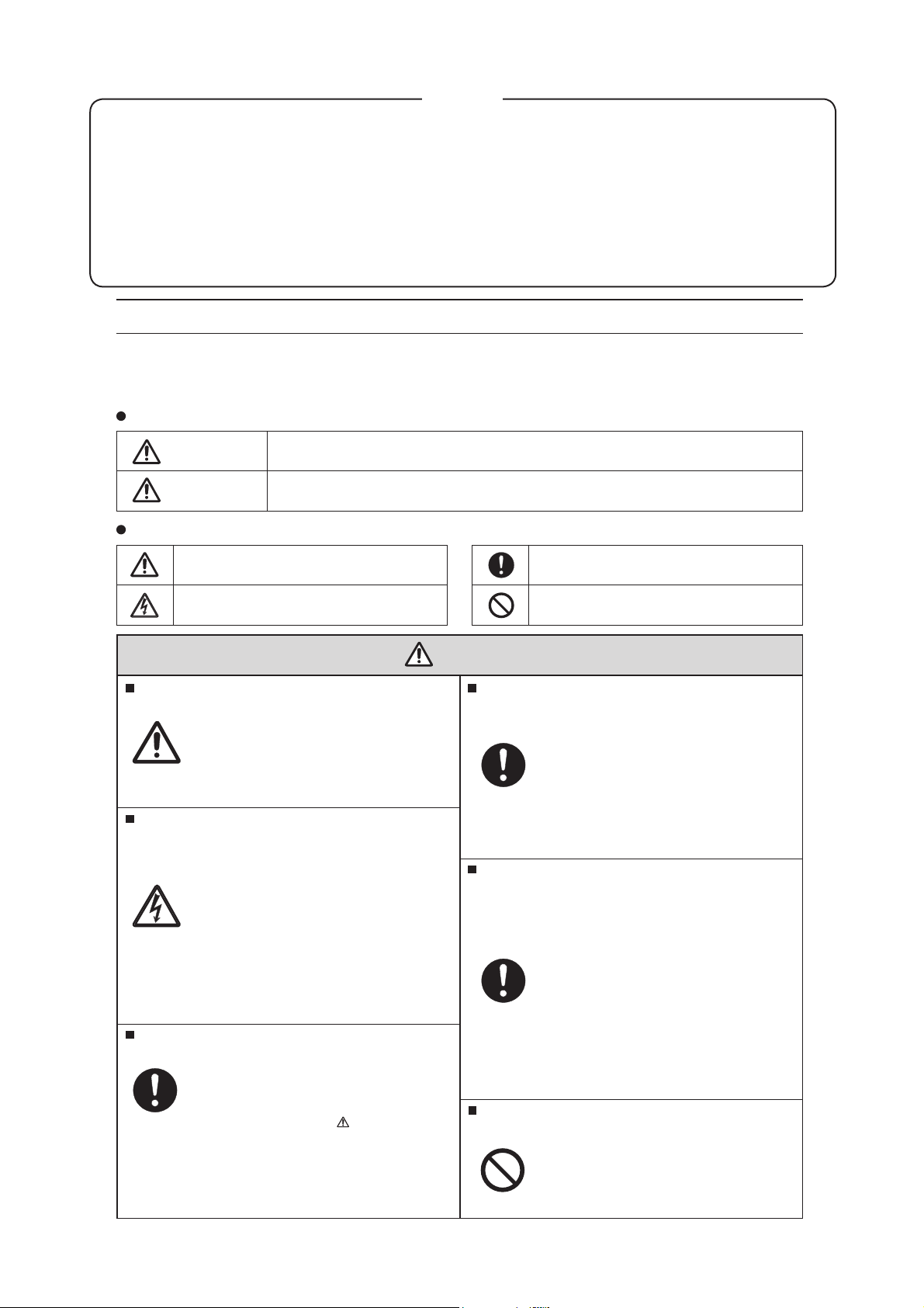
CAUTION FOR SAFETY
Please read this page before repairing the monitor.
This page explains the following items for keeping the safety of the set and preventing
accidents during repair work.
We explain by symbol, the damage or injury that can occur when taking wrong repair action.
Warning
Caution
This symbol means "possible to die or heavy damage"
This symbol means "possible to damage or something will break"
We made the symbol as below, which are kind of following items.
This symbol means "CAUTION"
This symbol means "POSSIBILITY of
ELECTRIC SHOCK"
This symbol means "MUST"
This symbol means "DO NOT"
WARNING
Should be followed instructions.
We indicate on cabinet, chassis and
parts by label, which are special
attention part.
Please follow notes and [Safety
Instructions] of User’s Manual.
Prevention of electric shock.
Please take care during working
because monitor has high voltage
parts and power supply parts.
Possible to die if you touch these
places by mistake.
Please disconnect power plug during
overhaul, reassembly or changing parts.
You may die or take damage by
electric shock if you touch live parts.
Use recommended components.
Please use same characteristic
component, which is same as previous
for your safety and keep reliability
especially marked by
circuit diagram.
There is risk of electric shock or fire
if you use non-recommended
component.
in parts list and
Should be kept same style of wiring or component.
Monitor uses tubes or tapes, which
made by insulator and some
components are keep distance from
surface of PWB for safety.
Internal leads kept from hot part or high
voltage part by clamper or styling, so
please return to original condition to
prevent electric shock or fire.
Should be done safety check after finished.
Every part (removed screws,
component and wiring) should be
returned to previous condition.
Check around repair position for
damage by mistake and measure the
insulated impedance by meg-ohm
meter.
Confirm the value of impedance, that
value is more than 4M ohm.
It is reason for electric shock or fire if
that value is less than 4M ohm.
Nobody can check and repair to the code
and combination circuit of HDCP.
Never remove the shield case, which is
assembled to the code and combination
circuit of HDCP.
1
Page 3

32LD9700U/32LD9700C/32LD9700N/37LD9700U/37LD9700C/37LD9700N
PRECAUTIONS
How to clean the LCD panel of the unit.
Wipe the panel with a lint-free and dry cloth in order to prevent damage to the panel surface.
Do not use a chemical cloth or cleaner. Depending on the ingredients, it may cause discoloration and
damage the panel surface.
Do not wipe with a hard cloth or rub hard. It may damage the panel surface.
In case of the greasy dirt such as fi ngerprint, wipe with a lint-free cloth moistened by a diluted neutral
detergent solution and then wipe with a soft, dry cloth.
Do not use a spray cleaner. It could cause malfunction.
How to clean the cabinet of the unit.
The following may cause cracks, deformation and paint peeling.
Do not wipe the cabinet with benzene, thinner or other chemical products.
Do not spray volatile solutions such as insecticide over the cabinet.
Do not leave the cabinet in prolonged contact with plastic or rubber materials.
Do not use a chemical cloth, cleaner or wax. Depending on the ingredients, it may cause cracks and
deformation.
Use a lint-free cloth to clean the cabinet and control panel of the monitor. In case of heavy dirt, wipe
with a soft cloth moistened by a diluted neutral detergent solution and then wipe with a soft, dry cloth.
Never use the following detergents. It could cause cracks, discoloration and scratches.
Acid/alkaline detergent, alcoholic detergent, abrasive cleaner, soap powder, OA cleaner, car wax, glass
cleaner, etc.
Information for users applicable in European Union countries
This symbol on the product or on its packaging means that your electrical and electronic
equipment should be disposed at the end of life separately from your household wastes.
There are separate collection systems for recycling in EU. For more information, please
contact the local authority or the dealer where you purchased the product.
2
Page 4
32LD9700U/32LD9700C/32LD9700N/37LD9700U/37LD9700C/37LD9700N
1. Features
Large-screen, high-definition LCD display panel (IPS-α panel)
The 32-inch, 37-inch color LCD display panel, with a resolution of 1366(H) x 768(V) pixels, creates a high-definition,
large-screen (aspect ratio : 16:9) and low-profile flat display. Free from electromagnetic interferences from
geomagnetic sources and ambient power lines, the panel produces high quality display images free from color
misconvergence and display distortion.
High Performance Digital Processor
A wide range of input signals can be handled, including composite, component and HDMI. High Definition Digital
Processor creates the fine textured image with dynamic contrast. In addition, it corresponds to a broad array of
personal computer signals, from 640 x 400 and 640 x 480 VGA to 1600 x 1200 UXGA.(Analog Input)
Easy-to-use remote control and on screen display system
The remote control included, eases the work of setting display controls. Further, the on-screen display
system, displays the status of signal reception and display control settings in an easy-to-view fashion.
Connecting to an Audio Visual Device
• Three Scart terminals
*1
, composite/S terminal*2, a component terminal*3 and two HDMI terminals have been
added. A composite video output terminal is also provided as a monitoring output.
*1
AV1 scart applies to composite/ S-video
AV2 and 3 scart applies to composite/ RGB
*2
AV5 composite/S-Video=Side Input
*3
AV4 can be connected to the equipment with either component or composite Output.
• A wide range of devices can also be connected besides personal computers.
SD card slot installed
Power Swivel Feature
It allows turning the plasma display left or right within ±30 degrees using the remote control.
Digital Terrestrial Television Broadcasting
Converting into digital signal enables to provide more channels and various useful features, such as Electric
Programme Guide, Digital Teletext and so on. Further, digital signal can create high quality picture.
Difference of broadcast signal method, divided into 32LD9700U/37LD9700U and 32LD9700C/37LD9700C
according to a country.
This logo indicates that the product is compliant with European Digital Broadcasting.
DVB is a registered trademark of the DVB Project.
This logo indicates that the product is set up to view digital terrestrial TV.
FREEVIEW and the FREEVIEW logo are trade marks of DVT Services Ltd and are used under license.
FREEVIEW Logo © DTV Services Ltd 2002.
This logo indicates that the product will work after implementation of full digital switchover.
The Digital logo is a Certification Mark.
3
Page 5
32LD9700U/32LD9700C/32LD9700N/37LD9700U/37LD9700C/37LD9700N
2. Specifications
SPECIFICATION
Panel
Net dimensions
Net weight
Ambient
conditions
Display dimensions
Resolution 1366 (H) x 768 (V) pixels 1366 (H) x 768 (V) pixels
Temperature Operating : 5°C to 35°C, Storage : 0°C to 40°C
Relative humidity Operating : 20% to 80%, Storage : 20% to 90% (non-condensing)
Power supply
Power consumption/ at standby
Audio output speaker total 20W speaker total 20W
(VIDEO input)
Input terminals
Approx. 32 inches
(698 (H) x 392 (V) mm, diagonal 801mm)
including Stand:
813(W)x663(H)x350(D) mm
excluding Stand:
813(W)x584(H)x114(D) mm
including Stand: 28.0kg
excluding Stand: 22.3kg
AC220 - 240V, 50Hz
163W/<1W 195W/<1W
AV1 : composite video input terminal (SCART)
S video input terminal (SCART)
L/R audio input terminal (SCART)
AV2•3 : composite video input terminal (SCART)
RGB video input terminal (SCART)
L/R audio input terminal (SCART)
AV4 : composite video input terminal (RCA)
component video input terminal.(RCA)
L/R audio input terminal (RCA)
AV5 : composite video input terminal (RCA)
S video input terminal (Mini DIN)
L/R audio input terminal (RCA)
HDMI 1•2 : HDMI input terminal
Audio input terminal (3.5mm Stereo Mini Jack)
Photo Input : Photo Input terminal / SD card slot
Approx. 37 inches
(820 (H) x 461 (V) mm, diagonal 941mm)
including Stand:
940(W)x736(H)x350(D) mm
excluding Stand:
940(W)x657(H)x119(D) mm
including Stand: 32.5kg
excluding Stand: 26.8kg
Input signals
Output Signal
(RF input)
Input terminal / Receiving range ANT : 75Ω Unbalanced / 44~870MHz
RF Video System
(RGB input)
Input terminals
Input signals 0.7 V/1.0 Vp-p, analogue RGB (Recommended Signal)
Sync signals
The unit takes at least 30 minutes to attain the status of optimal picture quality.
The SECAM D, K system might not be normally received, depending on the model.
Composite video: PAL, SECAM, NTSC3.58, NTSC4.43, PAL60
Component video: 480i, 576i, 480p, 576p, 720p/50, 720p/60, 1080i/50, 1080i/60
OUTPUT (MONITOR): composite video monitor-output terminal (RCA)
OUTPUT (MONITOR): L/R audio monitor- output terminal (RCA)
OUTPUT (HEADPHONE): L/R audio monitor- output terminal (Mini-pin)
OUTPUT (SUB-WOOFER): Woofer output terminal
AV1 : composite video output terminal (SCART)
L/R audio output terminal (SCART)
AV2•3 : composite video output terminal (SCART)
L/R audio output terminal (SCART)
PAL B, G, H / I / D, K
SECAM B, G / K1 / L, L' / (D,K)
DVB-T
Analogue RGB input terminal (D-sub 15-pin)
Audio input terminal (3.5mm Stereo Mini Jack)
H/V separate, TTL level [2KΩ]
H/V composite, TTL level [2KΩ]
Sync on green, 0.3 Vp-p [75Ω]
4
Page 6
32LD9700U/32LD9700C/32LD9700N/37LD9700U/37LD9700C/37LD9700N
3. Service points
Lead free solder
This product uses lead free solder (unleaded) to help preserve the environment. Please read these
instructions before attempting any soldering work.
Caution: Always wear safety glasses to prevent fumes or molten solder from getting into the eyes. Lead
free solder can splatter at high temperatures (600˚C).
Lead free solder indicator
Printed circuit boards using lead free solder are engraved with an "F."
Properties of lead free solder
The melting point of lead free solder is 40-50˚C higher than leaded solder.
Servicing solder
Solder with an alloy composition of Sn-3.0Ag-0.5Cu or Sn-0.7Cu is recommended.
Although servicing with leaded solder is possible, there are a few precautions that have to be taken. (Not
taking these precautions may cause the solder to not harden properly and lead to consequent malfunctions.)
Precautions when using leaded solder
Remove all lead free solder from soldered joints when replacing components.
If leaded solder should be added to existing lead free joints, mix in the leaded solder thoroughly after the
lead free solder has been completely melted (do not apply the soldering iron without solder).
Servicing soldering iron
A soldering iron with a temperature setting capability (temperature control function) is recommended.
The melting point of lead free solder is higher than leaded solder. Use a soldering iron that maintains a high
stable temperature (large heat capacity) and that allows temperature adjustment according to the part being
serviced, to avoid poor servicing performance.
Recommended soldering iron:
Soldering iron with temperature control function (temperature range: 320-450˚C)
Recommended temperature range per part:
Part Soldering iron temperature
Mounting (chips) on mounted PCB 320˚C±30˚C
Mounting (chips) on empty PCB 380˚C±30˚C
Chassis, metallic shield, etc. 420˚C±30˚C
The PWB assembly which has used lead free solder
SUBPOWER PWB (Subpower PWB, Filter PWB, Terminal PWB)
SOUND PWB (Audio PWB, Control PWB, SW PWB)
FC PWB
MAIN PWB (Main PWB, LED PDP PWB, Swivel PWB)
DTT PWB
5
Page 7
32LD9700U/32LD9700C/32LD9700N/37LD9700U/37LD9700C/37LD9700N
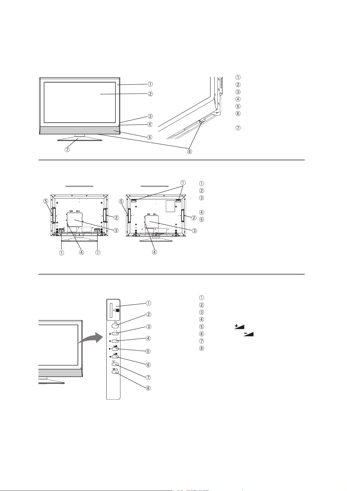
4. Component names
[Main unit]
Front Panel
Rear Panel
Cabinet
Panel
Indicating Lamp
Remote Control Receiver
Speaker
Main Power Switch
(on the bottom surface)
Desktop Stand
32” models 37” models
Control Panel (including Card Slot)
SD MEMORY
CARD
PUSH-EJECT
P
P
Handgrips
Side Input
Terminal Board (External Device
Connection)
Power Cord Socket
Control Panel (see below for details)
SD Memory Card Slot
Sub Power button
Channel UP/▲button
Channel DOWN/▼button
Volume UP
Volume DOWN
/►button
/◄button
Input Select /OK button
Menu / Return button
PH35814
OK
6
Page 8

32LD9700U/32LD9700C/32LD9700N/37LD9700U/37LD9700C/37LD9700N
[Remote control]
Sub Power
Function Select (TV/DVD/SAT)
Press this button to select function mode
indicating LED lamp.
Normally, select “
Input Select/DVD Control/Photo Input Control
Press this button to change input mode.
In addition, you can use these buttons while
operating the selected brand of DVD player or
Photo Input function.
Menu
Cursor
OK
Sound Mode
Sound mode can be changed each time pressed
in the following sequence. Movie→Music→
Speech→Favourite
CHI/II
This is exclusively for TV audio A2/NICAM mode.
Volume Up/Down
Programme Select
Press these buttons to select a TV program
directly.
Freeze/Multi Mode [Hold]
Press this button to change the picture to freeze
mode. Press it again to return to normal picture.
In addition, during multi-picture mode, each time
press this button, the picture is changed to 2, 4,
and 12 multi mode. (Also, it holds the page in
text mode.)
[Colour (Red, Green, Yellow, Blue)]
[Index]
Time [Cancel]
Pressing this button can indicate the time by OnScreen display when receiving a TV programme
on the screen.
TV/Text [TV
This switches between the TV mode and the
Teletext mode.
Zoom [Text
Press this button to change picture size.
Recall
Pressing this button shows the input signal
status.
Return
You can use this to return to the previous menu.
Picture Mode
Picture mode can be changed each time pressed
in the following sequence. Dynamic→Natural→
Cinema
Channel Up/Down
Mute
Multi Picture
Press this button to change the picture to multipicture mode. Press it again to return to normal
picture.
Photo Input (Photo/Rotate/Slide Show)
These buttons are to display and control the
pictures from digital still camera or USB card
reader.
Swivel (with Desktop Stand)
This function is to rotate TV. Select the degree
of rotation with cursor key.
TV”.
Text]
TV+Text]
7
Page 9

32LD9700U/32LD9700C/32LD9700N/37LD9700U/37LD9700C/37LD9700N
5. New adoption technology
[System control micom I001(M30627)]
Pin function table
No. PIN NAME I/O FUNCTION
VREF (+5.0V) I 5V
1
2
3
4
5
6
7 EXT_CONT_1
8 DATA_OUT(FC)
9 DATA_IN(FC)
10 CLK(FC)
11
12
13
14
15
16
17
18
19
20
21
22
23
24
25
26
27
28
29
30 EXT_CONT_2
31
32
33
34
35
36
37
38
39
40
41
42
43
44
45
46
47
48
49
50
+5.0V I 5V
AUDIO_SW1 I/O Audio SW1
OSD_DATA I/O OSD DATA
OSD_CLK I/O OSD CLK
HP_VOL
BL_INST I/O Black Insert On/Off for 32V LCD (37V=Low)
BL_BLINK I/O Backlight Blink On/Off for 32V LCD (37V=Low)
GND I GND
CNVSS(FLASH) I CNVSS(FLASH)
DSUB COMP I/O Sync Switching
RGB SW I/O Sync Switching
RESET I Reset
16MHz Oscillation O OSC-OUT
GND I GND
16MHz Oscillation I OSC-IN
+5.0V I 5V
NMI(+5.0V) I 5V PULL UP
RMCON I/O Receiving Remote Control Signal
NC I/O NC
V.FREQ_3 I/O V.Frequency
SCV.SYNC I/O SUB_Y.SYNC (Composite)
IRQ(PM-IRQ) I/O PDP Control
MCV.SYNC I/O MAIN_Y.SYNC (Composite)
POWER_LED I/O L:Lighting (Power Save)
CEC_OUT I/O CEC OUT(CEC1)
H.FREQ_3 I/O H.Frequency
PDWN
RXD2 I/O RS-232C Communication
TXD2 I/O RS-232C Communication
TXD1(RS232C/FLASH) I/O FLASH for Writing
RXD1(RS232C/FLASH) I/O FLASH for Writing
SCLK(FLASH) I/O FLASH for Writing
BUSY(FLASH) I/O FLASH for Writing
TXD0(DTT) I/O DTT
RXD0(DTT) I/O DTT
SDA4(panel) I/O PDP Communication(I2C Bus)
SCL4(panel) I/O PDP Communication(I2C Bus)
M_ENABLE I/O Media Enable
M_SCLK I/O
M_SDA I/O
M_WAKEUP I/O Media Wakeup
PDPGO(PM_ON) I/O PDP Control/LCD Panel 12V/WVGA Power
Panel:LCD
LCD
LCD
LCD
LCD
LCD
I/O Head Phone Volume
I/O
I/O FC MicroComputer 3 Lines Bus Data Out /Media Data Out
I/O FC MicroComputer 3 Lines Bus Data In/ Media Data In
I/O FC MicroComputer 3 Lines Bus Clock/ Media Clock
I/O External Control 2
I/O
I5V
IGND
LCD
LCD
LCD
LCD
LCD
LCD
LCD
LCD
LCD
LCD
LCD
LCD
LCD
LCD
LCD
LCD
LCD
LCD
LCD
LCD
LCD
LCD
LCD
LCD
LCD
LCD
LCD
LCD
LCD
LCD
LCD
LCD
LCD
LCD
LCD
LCD
LCD
LCD
LCD
LCD
LCD
LCD
LCD
LCD
LCD
External Control 1
Panel LVDS
Media Clock
Media Data
8
Page 10
32LD9700U/32LD9700C/32LD9700N/37LD9700U/37LD9700C/37LD9700N
No. PIN NAME I/O FUNCTION
CPUGO(PM_CPU) I/O PDP Control/Inverter Voltage
51
EPM (FLASH) I/O FLASH for Writing
52
VIDEO.DET_1 I/O
53
54
55
56
57
58
59
60
61
62
63
64
65
66
67
68
69
70
71
72
73
74
75
76
77
78
79
80
81
82
83
PDP_WVGA_LCD_SW_ I/O PDP/42WVGA/LCD Detection
84
85
86
87
88
89
90
91
92
93
94
95
PDP_WVGA_LCD_SW_ I/O PDP/42WVGA/LCD検出
96
97
98
99
100
SCL1 I/O
SDA1 I/O
HDMI-RESET I/O
HDMI-HPD_RESET I/O
SEL_0 I/O FC Clock/Others SW
SEL_1 I/O HDMI/DTT SW
TUNER.DET_1 I/O TUNER Detection
CE (FLASH) I/O FLASH for Writing
STAND.CIR_DET I/O Stand Detection
SW_L_OUT I/O
SW_R_OUT I/O
M_SW I/O Bridge Media Circuit Connection Judgement Terminal
INITIALIZE I/O Memory Initial
BR_MUTE I/O Bridge Media Audio Mute
CK_SEL I/O Clock Selector
SCDT I/O HDMI Power Save for Return
CK_INV I/O Clock Invert
DVI-SW I/O DVI Control
CUR_PRTCT I/O Power Swivel Overcurrent Detection
SP_MUTE I/O NC
AUDIO_MUTE I/O
ASEL1 I/O Audio Switching SW
ASEL2 I/O Audio Switching SW
SDA2 I/O I2C(TAS3103/TAS5508)
SCL2 I/O I2C(TAS3103/TAS5508)
D-SUB I/O
BM_SW I/O BM Switching
RGB_BLK_2 I/O RGB Blank 2
RGB_BLK_3 I/O RGB Blank 3
AUDIO_RESET I/O Audio Circuit Reset
+5.0V I
EDID_PROTECT_1 I/O Memory Protect(Not necessary if power is available to use)
GND I GND
WSS_1 I/O
WSS_2 I/O
WSS_3 I/O
TV.AFC(M) I/O Main Tuner Control (AFC)
TV.AFC(S) I/O Sub Tuner Control (AFC)
AUDIO_SW2 I/O Audio SW2
EDID_PROTECT_2 I/O Memory Protect(Not necessary if power is available to use)
HP_DETECT I/O HEAD PHONE DETECT
INT_HDMI I/O
CEC_IN I/O CEC IN(CEC2)
COMP_SW I/O Component SW / TV ⇔ DTT
DEMP_OUT I/O
Panel:LCD
LCD
LCD
LCD
LCD
LCD
LCD
LCD
LCD
LCD
LCD
LCD
LCD
LCD
LCD
LCD
LCD
LCD
LCD
LCD
LCD
LCD
LCD
LCD
LCD
LCD
LCD
LCD
LCD
LCD
LCD
LCD
LCD
LCD
LCD
LCD
LCD
LCD
LCD
LCD
LCD
LCD
LCD
LCD
LCD
VIDEO Board Detection
I2C(To the Side of Main Board) FE/MSP3455or MSP3415G/SDA6000
I2C(To the Side of Main Board) FE/MSP3455or MSP3415G/SDA6000
HDMI-Reset
Hot Plug Detect Reset
Swivel L Output
Swivel R Output
NC
D-SUB COMP for Sync Switching
SCART 1 Detedct
SCART 2 Detedct
SCART 3 Detedct
INT(HDMI)
De-emphasis Control Output for HDMI
9
Page 11

32LD9700U/32LD9700C/32LD9700N/37LD9700U/37LD9700C/37LD9700N
No. PIN NAME I/O FUNCTION
101
102
103
104
105
106
107
108
109
110
111
112 IRQ_DTT
113 DTT_POWER
114 DISPEN
115
116
117
118 SCL6
119 SDA6
120 COLOR_SYS
121
122
123
124
125
126
127
128
NC I/O NC
SCL0 I/O
SDA0 I/O
SCL3(EEPROM) I/O
SDA3(EEPROM) I/O
EPGGO I/O EPGGO
EXT_RESET I/O EXTERNAL RESET
OSD_CS I/O OSD CS
FC_ENABLE I/O FC MicroComputer 3 Lines Enable
V_P_DET_1 I/O V_DET_1(Power Save Return)
V_P_DET_2 I/O
HDMI_A_SW I/O HDMI AUDIO SW
SCL5 I/O
SDA5 I/O
AD_KEY3 I/O AD KEY3**
AD_KEY2 I/O AD KEY2*
AD_KEY1 I/O AD KEY1(Power)
TV.POWER I/O H:PowerON、L:(Standby,PowerSave)
DIP.DET I/O DIP DET
POWER_SAVE I/O L:Lighting(Standby、PowerSave), H:Lights-out
GND I GND
FAN_ALARM *1 I/O FAN ALARM
Panel:LCD
LCD
LCD
LCD
LCD
LCD
LCD
LCD
LCD
LCD
LCD
LCD
I/O DTT IRQ
I/O DTT POWER
I/O DISPEN/Backlight on
LCD
LCD
LCD
LCD
LCD
LCD
I/O I2C(To the Side of Sensor Board) (AD7414)
I/O I2C(To the Side of Sensor Board) (AD7414)
I/O Color System (Pull-in range Switching)
LCD
LCD
LCD
LCD
LCD
LCD
LCD
LCD
LCD
LCD
LCD
2
C(To the Side of Main Board) (TA1391FG/CXA2069/uPD64015/TB1274AF)
I
2
I
C(To the Side of Main Board) (TA1391FG/CXA2069/uPD64015/TB1274AF)
2
I
C(EEPROM)
2
I
C(EEPROM)
Power Delay
2
C(Sil9021)
I
2
I
C(Sil9021)
10
Page 12
MAIN μ-COMPUTE
R
(M30627)
T
E
SCDT
P43
P97AUDIO_SW
(CAT24WC64)
V
K
EDID_PROTECT_1
P30
P04
EXT
RESET
䇼
A0/A1h䇽A
T
A
A
A
V
R
IRQ(PM
IRQ)
P80
P17PDP
WVGA
LCD
SW1
(TB1274)
(ENG39616G
*1/V0
A31FTV *2/ENG29
**G *3)
(TAS3103)
A
T
CPUGO(PM
CPU)
P56
P130
HDMI_HPD_RESET
䇼
8E/8Fh
䇽
䇼
C0h
䇽
䇼
6Ah
䇽
)
T
W
X
R
V
FREQ
3
INT0
(H8S_2239 )
(CXA2069Q)
(MSP3415G*
䋯
MSP3455G *4)
(TAS5508
䋩
AD
KEY3
AN6
P02
ENABLE
S
4
COMP_DET_AV1
䇼
80/81h
䇽
䇼
36h䇽A
AN5A
A
EDID
PROTECT
2
P21
AN25WSS_3
(OSDCM201 )
S2-3
(ENG39616G)
A
TV.AFC(M)
AN24
SOUT4
SIN䇼90/91h䇽SDA1
A
A
RESET
RESET
3D
Y/C
䇼
C6h䇽HDMI_A
SW
P114
P137M
ENABLE
(uPD64015)
2
A
FAN
ALARM
P100
P134
M_WAKEUP
TV.SEL_4
WVGA PANEL
SCL6
P111
P124
BM_SW
䇼
B8h
䇽
SCL1
TV
SEL_1
FUNC_2
P110
P123
RGB_BLK_2
SDA1
TV.SEL_2
SCL4
DIP_DET
P102
(TA1391FG)
䇼
60/61h䇽FE.SW_2
DTT
TXD0
RXD2
RS232C
SCL0
AGC
HP_DETECT
AN20
P60䇼D8/D9h
䇽
L
IRQ_DTT
P117P113
HDMI
NC
P12
P112
(Sil9023)
SCL4
T
C
COMP_SW
P14
P64
BUSY(FLASH)
SDA
M62342G
TXD1
FLASH_TXD
SCL4
INT (HDMI)
P16
RXD1
FLASH_RXD
䇼
68/69h䇽SDA4
EPGGO
P05P50CEN
l
0V5V
0V
HP_VOL DA1 P54 VIDEO.DET_1
DSUB COMP P87 P53 SEL_2
RGB SW P86 P52 SEL_1
POWER_SAVE P101 P51 TUNER.DET
POWER_LED P76
M_SCK P136 P127 STAND.CIR_DE
TV.POWER P103 P126 SW_L_OUT
BR_MUTE P45 P125 SW_L_OUT
CK_SEL P44 P46 INITIALIZ
CK_IN
DVI-SW P41 P07 SCL3
BL_BLIN
UD RST P121 P115 DISPEN
CUR_PRTC
SP_MUTE P37 P33
UDIO_MUTE P36 P133
SEL1 P35 P132
SEL2 P34 P11
PDWN P72 P10
V_P_DET_1 P01
-
M_SD
PDPGO(PM_ON) P57 P131 HDMI_RESE
_
RMCON(AVC
CEC_OU
.
11
_
V_P_DET_2 P00 CLK3 CLOCK SCL0 S-1 SCL1 SCL2
SCV.SYNC TA4IN SOUT3 DATA IN SDA0 S-2 S_DET_AV3 SDA1 SDA2
MCV.SYNC TA3IN SIN3 DATA OUT S-3 COMP_DET_AV2 RESET MSP_RESET
_
D_KEY2
UDIO_SW2 P22 AN26 WSS_2 OSD CONTROLLER S2-3 FE Sub
_
TV.AFC(S)
D_KEY1
H.FREQ_3 TA1IN M_SCLK SCL0
FUNCTION_
BL_INST P141 P122 RGB_BLK_3 SYNC SEPARATION FE.SW_1 SDA4
_
_
_
P42 P47 M_SW
P140 P06 SDA3
P40 P32
DA0 P120 PDP_WVGA_LCD_SW2 SCL0 SCL1 SCL2
P135 SDA0 SDA1 SDA2
P84
TA2OUT FC SUB μ-com AV S
N27 WSS_1 S2-2
N23 CLK4 SCLK S2-4 SCL1
N4 P03 CS
P75 M_SD
_
_
_
_
_
EEPROM
䌐120
P17
PANEL TYPE
10
32LCD
11
37LCD
IDEO DECODER TUNER (FE Main) AUDIO PROCESSO
SOUND MULTIPLE
-
L
SDA0 TELETEXT TV.SEL_3
(SDA6000)
*3䇼84/85h䇽
5
-
5
.
AUDIO PROCESSO
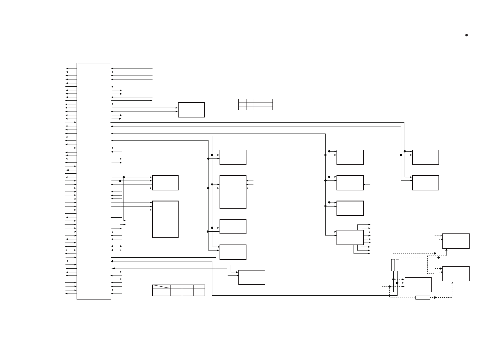
Block diagram
32LD9700U/32LD9700C/32LD9700N/37LD9700U/37LD9700C/37LD9700N
DTT RXD0 TXD2 RS232C SDA0 Text Ys_SW
DTT_POWER P116 P61
DEMP_OU
CEC_IN P15 CNVss CE EPM CNVss P56
COLOR_SYS P107 P55 EPM Flash Writing 5V 0V 5V
13PBUS-D
P13 P65 SCLK(FLASH) SCL5 DA
orma
5
S_Trap
LCD PANE
Buffer
Buffer
Level
SDA4
Page 13

32LD9700U/32LD9700C/32LD9700N/37LD9700U/37LD9700C/37LD9700N
6. Adjustment
● How to get to Adjustment mode
Using the R-side control buttons with the set turned off (standby) can activate it.
Press the SUB-POWER(
more than 5 seconds.
The set turns on in adjustment mode with OSD.
● Changing data and Selecting Adjustment code
When the set is in adjustment mode, the cursor , , , and OK buttons of the remote control or R-side
control buttons may be used as the adjustment keys.
, buttons are used for selecting adjustment code.
, buttons are used for changing data values.
OK button is used for confirming the data.
After finishing the necessary adjustment press MENU button. Adjustment mode is released and the set
returns to normal condition.
● Memory Initialize operation
NOTE: The execution of this function returns the adjustment codes to the preset values, therefore,
adjustment data will be lost.
Procedure
(1) Enter Adjustment Mode.
(2) Select MEMORY INIT adjustment code (No.898) and change the data value from 0 to 1.
(3) Activate MEMORY INIT by pressing OK button.
(4) Select No.712 and change data value from 1 to 0.
(5) Check that the receiving channel goes to P1. Unit is set to preset values.
) button, INPUT SELECT( ) button and button at the same time and hold for
● How to check method of the use accumulation time for panel.
Select No. 894 of Service Adjustment Menu.
( *When No.894 is displayed as “65535” select No.893 and change data value from 0 to 1. Check No.894 is
displayed as “0”.)
12
Page 14
32LD9700U/32LD9700C/32LD9700N/37LD9700U/37LD9700C/37LD9700N
Service
Adj.
No
0 SUB_CONTRAST (AV1) Sub Composite mode 15 8 TB1274
1 SUB_CONTRAST (AV2) Sub Composite mode 15 8 TB1274
2 SUB_CONTRAST (AV3) Sub Composite mode 15 8 TB1274
3 SUB_CONTRAST (AV4) Sub Composite mode 15 8 TB1274
4 SUB_CONTRAST (AV5) Sub Composite mode 15 8 TB1274
5 SUB_CONTRAST (RF) Sub 15 8 TB1274
6 Sub Color Sub 15 8 TB1274
7 TINT (RF) Sub 63 33 TB1274
8 TINT (VIDEO) Sub 63 31 TB1274
9 Reference Amplitude(RGB_AMP) RF/VIDEO 254 127 FC
10 Reference Amplitude(RGB_AMP) PC 254 127 FC
11Reference Amplitude(RGB_AMP) Multi Picture mode 254 130 FC
12 Display for Max. Amplitude Level Main - - FC
13 Display for Max. Amplitude Level Sub - - FC
14 Set Blue Gamma gain On/Off 0:Off, 1:On (For 55V) For 55V 1 1 FC
15 Contrast mode<Dynamic> SW (TV) 0:Dynamic, 1:Dynamic+Auto RF 1 1 FC
16 APL Enhancer 0:OFF, 1:ON For Dynamic mode 1 1 FC
17 HDMI PC Function 0:OFF, 1:ON (for customer request) 1 0
18 PinP Function (for PC) 0:PinP, 1:Infomation1, 2:Infomaiton Split 2 0 FC
19 Black Level(RGB_AMP) RF/VIDEO 254 127 FC
20 Black Level(RGB_AMP) PC 254 127 FC
21 Black Level(RGB_AMP) For USA NTSC/480i 254 127 FC
22 Protect for Image Retention 0:Off, 1:7%, 2:14%, 3:21%, 4:AUTO Dynamic mode 4 4 FC
23 Protect for Image Retention 0:Off, 1:7%, 2:14%, 3:21%, 4:AUTO Natural mode 4 4 FC
24 Protect for Image Retention 0:Off, 1:7%, 2:14%, 3:21%, 4:AUTO Cinema mode 4 4 FC
25 YNR Input Level RF 7 7 FC
26 YNR Input Level VIDEO 7 7 FC
27 YNR Input Level Scart-RGB(50/60Hz) 7 7 FC
28 YNR Input Level 480i/576i 7 7 FC
29 YNR Input Level 480p/576p 7 7 FC
30 YNR Input Level for AV1-5 Mode 1080i-50/60/720p 7 7 FC
31 YNR Input Level for →HDMI Mode 480i/480p/576i/576p/VGA 7 7 FC
32 YNR Input Level for →HDMI Mode 1080i-50/60/720p 7 7 FC
33 CNR Input Level at Low level for AV1-5 Mode RF/VIDEO 7 3 FC
34 CNR Input Level at Low level for AV1-5 Mode Scart-RGB(50/60Hz) 7 3 FC
35 CNR Input Level at Low level for AV1-5 Mode 480i/576i 7 3 FC
36 CNR Input Level at Low level for AV1-5 Mode 480p/576p 7 3 FC
37 CNR Input Level at Low level for AV1-5 Mode 1080i-50/60/720p 7 3 FC
38 CNR Input Level at Low level for →HDMI Mode 480i/480p/576i/576p/VGA 7 2 FC
39 CNR Input Level at Low level for →HDMI Mode 1080i-50/60/720p 7 2 FC
40 Main/Sub YFRNR Pass Level [MYNRP0] NTSC/PAL/Multi 7 1 FC
41 [MYNRP5] NTSC/PAL-VIDEO 7 0 FC
42 [MYNRP6'] Scart-RGB(50/60Hz) 7 0 FC
43 [MYNRP6] 480i/576i (Except HDMI) 7 0 FC
44 [MYNRP7] 480p/576p (Except HDMI) 7 0 FC
45 [MYNRP8] 1080i-50/60/720p (Except HDMI) 7 0 FC
46 [MYNRP6] 480i/576i (HDMI) 7 0 FC
47 [MYNRP7] 480p/576p (HDMI) 7 0 FC
48 [MYNRP8] 1080i-50/720p-50 (HDMI) 7 1 FC
49 [MYNRP8'] 1080i-60/720p-60 (HDMI) 7 0 FC
50 Main/Sub CFRNR Pass Level [MCNRP0] NTSC/PAL/Multi 7 0 FC
51 [MCNRP5] NTSC/PAL-VIDEO 7 0 FC
52 [MCNRP6'] Scart-RGB(50/60Hz) 7 0 FC
53 [MCNRP6] 480i/576i 7 0 FC
54 [MCNRP7] 480p/576p 7 0 FC
55 [MCNRP8] 1080i-50/60/720p 7 0 FC
56 Vertical Enhancer Gain for B-Y/B, R-Y/R [CVEG0] NTSC/PAL/480i/576i/Multi 15 15 FC
57 [CVEG1] 480p/576p/1080i-50/60/720p 15 9 FC
58 Vertical DSB Gain for B-Y/B, R-Y/R [CVDSBG0] NTSC/PAL/480i/576i/Multi 3 0 FC
59 [CVDSBG1] 480p/576p/1080i-50/60/720p 3 0 FC
adjustment items by I
ADJ. Items Mode
2
C-bus control (MAIN Part)
Function
Max.
value
Init.
Value
Device
13
Page 15

32LD9700U/32LD9700C/32LD9700N/37LD9700U/37LD9700C/37LD9700N
Adj.
No
60 Vertical DSB coring for B-Y/B, R-Y/R [CVDSBC0] NTSC/PAL/480i/576i/Multi 7 0 FC
61 [CVDSBC1] 480p/576p/1080i-50/60/720p 7 0 FC
62 Vertical Enhancer CLIP 0:CTI for B-Y/B, R-Y/R [CVECLP0] NTSC/PAL/480i/576i/Multi 1 0 FC
63 [CVECLP1] 480p/576p/1080i-50/60/720p 1 0 FC
64 Horizontal HPF Peak Frequency Switch for B-Y/B, R-Y/R [CHHPF0] NTSC/PAL/480i/576i/Multi 3 2 FC
65 [CHHPF1] 480p/576p/1080i-50/60/720p 3 2 FC
66 Horizontal Enhancer Gain for B-Y/B, R-Y/R [CHEG0] NTSC/PAL/480i/576i/Multi 15 15 FC
67 [CHEG1] 480p/576p/1080i-50/60/720p 15 9 FC
68 Horizontal DSB Gain for B-Y/B, R-Y/R [CHDSBG0] NTSC/PAL/480i/576i/Multi 3 0 FC
69 [CHDSBG1] 480p/576p/1080i-50/60/720p 3 0 FC
70 Horizontal DSB Coring for B-Y/B, R-Y/R [CHDSBC0] NTSC/PAL/480i/576i/Multi 7 0 FC
71 [CHDSBC1] 480p/576p/1080i-50/60/720p 7 0 FC
72 Horizontal Enhancer CLIP 0:CTI for B-Y/B, R-Y/R [CHECLP0] NTSC/PAL/480i/576i/Multi 1 0 FC
73 [CHECLP1] 480p/576p/1080i-50/60/720p 1 0 FC
74 B-Y Clamp Offset NTSC/PAL/480i/576i/480p/576p 255 128 FC
75 R-Y Clamp Offset NTSC/PAL/480i/576i/480p/576p 255 128 FC
76 B-Y Clamp Offset 1080i-50/60 255 127 FC
77 R-Y Clamp Offset 1080i-50/60 255 127 FC
78 B-Y Clamp Offset 720p 255 128 FC
79 R-Y Clamp Offset 720p 255 128 FC
80 B-Y Clamp Offset →[HDMI] 480i/576i/480p/576p/VGA 255 128 FC
81 R-Y Clamp Offset →[HDMI] 480i/576i/480p/576p/VGA 255 128 FC
82 B-Y Clamp Offset →[HDMI] 1080i-50/60 255 128 FC
83 R-Y Clamp Offset →[HDMI] 1080i-50/60 255 128 FC
84 B-Y Clamp Offset →[HDMI] 720p 255 128 FC
85 R-Y Clamp Offset →[HDMI] 720p 255 128 FC
86 FC6 THROUGH 0:OFF, 1:THROUGH ON 1 0 FC
87 Dynamic Back Light Correction For LCD 1 1 FC
88 Dynamic Contrast Correction 11 FC
89 Histogram Color Management 11 FC
90 Histogram Gradation Amp. 11 FC
91 Histogram Enhancer 11 FC
92 Dynamic Enhancer 11 FC
93 Main H Sync Phase Adjustment (MHPHS) DTT 255 122 FC
94 Sub H Sync Phase Adjustment (SHPHS) DTT 255 132 FC
95 P/N ID Sub 1 0 TB1274
96 Sharpness Gain(RF/NR) Sub 15 2 TB1274
97 Sharpness Gain(RF) BG/DK/I Sub 15 8 TB1274
98 Sharpness Gain(RF) M Sub 15 8 TB1274
99 Sharpness Gain(RF) L Sub 15 8 TB1274
100 Sharpness Gain(RF) L' Sub 15 8 TB1274
101 Sharpness Gain(VIDEO) PAL Sub 15 10 TB1274
102 Sharpness Gain(VIDEO) NTSC3.58 Sub 15 10 TB1274
103 Sharpness Gain(VIDEO) SECAM,B/W Sub 15 10 TB1274
104 Sharpness Gain(VIDEO) NTSC4.43 Sub 15 10 TB1274
105 Sharpness Gain(VIDEO) N-PAL Sub 15 10 TB1274
106 Sharpness Gain(VIDEO) M-PAL Sub 15 10 TB1274
107 Sharpness Gain(S.VIDEO) Sub 15 8 TB1274
108 Sharpness f0(RF) BG/DK/I Sub 3 2 TB1274
109 Sharpness f0(RF) M Sub 3 2 TB1274
110Sharpness f0(RF) L Sub 3 2 TB1274
111 Sharpness f0(RF) L' Sub 3 2 TB1274
112Sharpness f0(VIDEO) PAL Sub 3 2 TB1274
113Sharpness f0(VIDEO) NTSC3.58 Sub 3 2 TB1274
114Sharpness f0(VIDEO) SECAM,B/W Sub 3 2 TB1274
115Sharpness f0(VIDEO) NTSC4.43 Sub 3 2 TB1274
116Sharpness f0(VIDEO) N-PAL Sub 3 2 TB1274
117Sharpness f0(VIDEO) M-PAL Sub 3 2 TB1274
118Y Out Level M (4.5) Sub 63 10 TB1274
119Y Out Level B/G (5.5) Sub 63 13 TB1274
ADJ. Items Mode
Function
Max.
value
Init.
Value
Device
14
Page 16

32LD9700U/32LD9700C/32LD9700N/37LD9700U/37LD9700C/37LD9700N
Adj.
No
120 Y Out Level D/K (6.5) Sub 63 12 TB1274
121 Y Out Level I (6.0) Sub 63 13 TB1274
122 Y Out Level L (6.5) Sub 63 12 TB1274
123 Y Out Level L' (6.5) Sub 63 15 TB1274
124 Y Out Level (VIDEO) Sub 63 10 TB1274
125 Y Out Level (TEXT) Sub 63 4 TB1274
126 C Out Level M (4.5) Sub 63 12 TB1274
127 C Out Level B/G (5.5) Sub 63 8 TB1274
128 C Out Level D/K (6.5) Sub 63 8 TB1274
129 C Out Level I (6.0) Sub 63 7 TB1274
130 C Out Level L (6.5) Sub 63 7 TB1274
131 C Out Level L' (6.5) Sub 63 7 TB1274
132 C Out Level (VIDEO) Sub 63 10 TB1274
133 C Out Level (TEXT) Sub 63 8 TB1274
134 BPF_Q (4.43MHz) Sub 3 3 TB1274
135 BPF_f0 (4.43MHz) Sub 3 1 TB1274
136 C_TRAP_SW (COMB=OFF-PAL/NTSC4.43/NTSC3.58) Sub 1 0 TB1274
137 LPF Sub 1 0 TB1274
138 SECAM D-Trap Sub 1 1 TB1274
139 FILTER SW(RF) Sub 1 0 TB1274
140 Y_DL (4.5MHz) Sub 10 5 TB1274
141 Y_DL (5.5MHz PAL/NTSC4.43) Sub 10 2 TB1274
142 Y_DL (5.5MHz SECAM) Sub 10 0 TB1274
143 Y_DL (6.0PAL/NTSC4.43) Sub 10 7 TB1274
144 Y_DL (6.0SECAM) Sub 10 5 TB1274
145 Y_DL (6.5PAL/NTSC4.43) Sub 10 5 TB1274
146 Y_DL (6.5SECAM) Sub 10 5 TB1274
147 Y_DL (L) Sub 10 5 TB1274
148 Y_DL (L') Sub 10 5 TB1274
149 Y_DL (VIDEO PAL/NTSC4.43) Sub 10 5 TB1274
150 Y_DL (VIDEO SECAM) Sub 10 5 TB1274
151 Y_DL (VIDEO NTSC) Sub 10 5 TB1274
152 NTSC Comb(Comb off) Sub 1 1 TB1274
153 Cb offset1 Sub 15 8 TB1274
154 Cr offset1 Sub 15 8 TB1274
155 MVM (VIDEO) 1 0 TB1274
156 AFC_GAIN (AV00) 3 0 TB1274
157 AFC_GAIN (AV1) 3 0 TB1274
158 AFC_GAIN (AV2) 3 0 TB1274
159 AFC_GAIN (AV3) 3 0 TB1274
160 AFC_GAIN (AV4) 3 0 TB1274
161 AFC_GAIN (AV5) 3 0 TB1274
162 AFC_GAIN (Except AV00) 3 0 TB1274
163 S_B-Y_ADJ Sub 15 8 TB1274
164 S_R-Y_ADJ Sub 15 8 TB1274
165 BELL_f0 Sub 1 0 TB1274
166 S_INHBT 1 0 TB1274
167 S_ID 1 0 TB1274
168 S_GP 3 0 TB1274
169 S_V_ID 1 0 TB1274
170 BELL/HPF 3 3 TB1274
171 HS Phase Sub 1 0 TB1274
172 Bandwidth 1 NTSC/PAL/480i/576i 3 1 TA1391FG
173 Bandwidth 1 480p/576p 3 2 TA1391FG
174 Bandwidth 1 1080i-50/60/720p 3 0 TA1391FG
175 Bandwidth 1 DTT 3 2 TA1391FG
176 Bandwidth 2 NTSC/PAL/480i/576i 3 2 TA1391FG
177 Bandwidth 2 480p/576p 3 2 TA1391FG
178 Bandwidth 2 1080i-50/60/720p 3 0 TA1391FG
179 Bandwidth 2 DTT 3 2 TA1391FG
ADJ. Items Mode
Function
Max.
value
Init.
Value
Device
15
Page 17

32LD9700U/32LD9700C/32LD9700N/37LD9700U/37LD9700C/37LD9700N
Adj.
No
180 Sub Contrast 1 Except 15kHz system (15kHz→#262) 15 0 TA1391FG
181 Sub Contrast 1 DTT 15 0 TA1391FG
182 Sub Contrast 2 15 0 TA1391FG
183 Sub Contrast 2 DTT 15 0 TA1391FG
184 Sub Color 1 15 12 TA1391FG
185 Sub Color 1 DTT 15 0 TA1391FG
186 Sub Color 2 15 8 TA1391FG
187 Sub Color 2 DTT 15 0 TA1391FG
188 HV THRU 1 NTSC/PAL/480i/576i/480p/576p 1 0 TA1391FG
189 HV THRU 1 1080i-50/60/720p 1 0 TA1391FG
190 HV THRU 2 NTSC/PAL/480i/576i/480p/576p 1 0 TA1391FG
191 HV THRU 2 1080i-50/60/720p 1 0 TA1391FG
192 H_SEP 1 RF/VIDEO 1 0 TA1391FG
193 H_SEP 1 480i/576i 1 0 TA1391FG
194 H_SEP 1 480p/576p 1 0 TA1391FG
195 H_SEP 1 1080i_50 1 0 TA1391FG
196 H_SEP 1 1080i_60/720p 1 0 TA1391FG
197 H_SEP 2 RF/VIDEO 1 0 TA1391FG
198 H_SEP 2 480i/576i 1 0 TA1391FG
199 H_SEP 2 480p/576p 1 0 TA1391FG
200 H_SEP 2 1080i_50 1 0 TA1391FG
201 H_SEP 2 1080i_60/720p 1 0 TA1391FG
202 V_SEP 1 RF/VIDEO 1 0 TA1391FG
203 V_SEP 1 480i/576i 1 0 TA1391FG
204 V_SEP 1 480p/576p 1 0 TA1391FG
205 V_SEP 1 1080i_50 1 0 TA1391FG
206 V_SEP 1 1080i_60/720p 1 0 TA1391FG
207 V_SEP 2 RF/VIDEO 1 0 TA1391FG
208 V_SEP 2 480i/576i 1 0 TA1391FG
209 V_SEP 2 480p/576p 1 0 TA1391FG
210 V_SEP 2 1080i_50 1 0 TA1391FG
211V_SEP 2 1080i_60/720p 1 0 TA1391FG
212 AFC MODE 1 RF 3 0 TA1391FG
213 AFC MODE 1 VIDEO 3 0 TA1391FG
214 AFC MODE 2 RF 3 0 TA1391FG
215 AFC MODE 2 VIDEO 3 0 TA1391FG
216 N_LVL 1 RF 1 0 TA1391FG
217 N_LVL 1 VIDEO 1 0 TA1391FG
218 N_LVL 2 RF 1 0 TA1391FG
219 N_LVL 2 VIDEO 1 0 TA1391FG
220 HD POSITION 1 480i/576i 15 0 TA1391FG
221 HD POSITION 1 480p/576p 15 0 TA1391FG
222 HD POSITION 1 1080i_50 15 0 TA1391FG
223 HD POSITION 1 1080i_60/720p 15 0 TA1391FG
224 HD POSITION 2 480i/576i 15 0 TA1391FG
225 HD POSITION 2 480p/576p 15 0 TA1391FG
226 HD POSITION 2 1080i_50 15 0 TA1391FG
227 HD POSITION 2 1080i_60/720p 15 0 TA1391FG
228 Y LPF 1 RF 1 1 TA1391FG
229 Y LPF 1 VIDEO 1 1 TA1391FG
230 Y LPF 2 RF 1 1 TA1391FG
231 Y LPF 2 VIDEO 1 1 TA1391FG
232 Gain 1 1 1 TA1391FG
233 Gain 2 1 1 TA1391FG
234 HD/VD OUTPUT LEVEL 1 1 TA1391FG
235 Video2-RGB MODE ON For ASIA 1 0 236 Heat APC function (HAPC) available 1 1 PDP
237 γ-select(0:1.0, 1:2.2, 2:2.8) RF/VIDEO 2 1 PDP
238 γ-select(0:1.0, 1:2.2, 2:2.8) DSUB-RGB 2 1 PDP
239 Select for APC function 1 0 PDP
ADJ. Items Mode
Function
Max.
value
Init.
Value
Device
16
Page 18

32LD9700U/32LD9700C/32LD9700N/37LD9700U/37LD9700C/37LD9700N
Adj.
No
240 CCFMD function RF/VIDEO 1 0 PDP
241 CCFMD function DSUB-RGB 1 0 PDP
242 NTSC/EBU(CCFORM) SD(YCbCr)/Scart-RGB 1 0 PDP
243 NTSC/EBU(CCFORM) HD(YPbPr) 1 0 PDP
244 NTSC/EBU(CCFORM) DSUB-RGB 1 0 PDP
245 Correction for Tracking (DCBON) RF/VIDEO-Color Temp. Cool 1 1 PDP
246 Correction for Tracking (DCBON) RF/VIDEO-Color Temp. Nor/War 1 1 PDP
247 Correction for Tracking (DCBON) DSUB-RGB 1 1 PDP
248 Color Temp. Correction 3 2 PDP
249 Brightness Limitted Function of PANEL [APSON] 1 1 PDP
250 Dispersion Time of Sustain current 0:2 Times, 1:4 times For Dynamic mode 1 0 PDP
251 Dispersion Time of Sustain current 0:2 Times, 1:4 times For Natural mode 1 1 PDP
252 Dispersion Time of Sustain current 0:2 Times, 1:4 times For Cinema mode 1 1 PDP
253 Dispersion Time of Sustain current 0:2 Times, 1:4 times For PC mode 1 1 PDP
254 Dispersion Time of Sustain current 0:2 Times, 1:4 times For PC-Movie mode 1 1 PDP
255 Q mode 0:Freeze, 1:Move 1, 2:Move 2, 3:Movie3 For 50Hz[Dynamic] mode 3 1 PDP
256 Q mode 0:Freeze, 1:Move 1, 2:Move 2, 3:Movie3 For 50Hz[Natural] mode 3 1 PDP
257 Q mode 0:Freeze, 1:Move 1, 2:Move 2, 3:Movie3 For 50Hz[Cinema] mode 3 1 PDP
258 Q mode 0:Freeze, 1:Move 1, 2:Move 2, 3:Movie3 For 60Hz[Dynamic] mode 3 1 PDP
259 Q mode 0:Freeze, 1:Move 1, 2:Move 2, 3:Movie3 For 60Hz[Natural] mode 3 1 PDP
260 Q mode 0:Freeze, 1:Move 1, 2:Move 2, 3:Movie3 For 60Hz[Cinema] mode 3 1 PDP
261 Q mode 0:Freeze, 1:Move 1, 2:Move 2, 3:Movie3 For 70Hz(PC) 3 0 PDP
262 Sub Contrast 1 15kHz System 15 4 TA1391FG
263 Vak OFfSet (Vak_OFS) 255 0 PDP
264 Vak to Vra Parameter(VaktoVra) 255 1 PDP
265 Vsk to Vrs Parameter(VsktoVrs) 255 1 PDP
266 VFB WAIT CounTer(CT_VWAIT) 255 60 PDP
267 VFB CORRection Counter(CT_VCORR) 255 15 PDP
268 Vsk OFFSet(Vsk_OFS) 255 0 PDP
269 Uvrs/Uvra RECALL(RCLVr) 1 0 PDP
270 C3OTON 1:ON, 0:OFF 1 1 PDP
271 C3OTLV 1:ON, 0:OFF 1 1 PDP
272 SRV16 1:ON, 0:OFF 1 0 PDP
273 WTI-VW 1:ON, 0:OFF 1 0 PDP
274 WTI-WAVE 0:AUTO1, 1:AUTO2, 2:Fix 2 0 PDP
275 SPD OFF 0:ON, 1:OFF PC mode 1 0 PDP
276 Vsk DETect First 2Bits(Vsk_DET) - - PDP
277 Vsk DETect Last 8Bits(Vsk_DET) - - PDP
278 Vsk detect INIT. First 2Bits(Vsk_INIT) - - PDP
279 Vsk detect INIT. Last 8Bits(Vsk_INIT) - - PDP
280 Vak DETect First 2Bits(Vak_DET) - - PDP
281 Vak DETect Last 8Bits(Vak_DET) - - PDP
282 DeLTa Vrs value(DLT_Vrs) - - PDP
283 DeLTa Vra value(DLT_Vra) - - PDP
284 Vak detect INIT. First 2Bits(Vak_INIT) - - PDP
285 Vak detect INIT. Last 8Bits(Vak_INIT) - - PDP
286 USER Vrs(Uvrs) - - PDP
287 USER Vra(Uvra) - - PDP
288 ISM Limit Limit Value 0:1023 1:580 1 0 WVGA
289 ISM Control for WVGA For WVGA 1 1 WVGA
290 SWIVEL DEMO MODE ON 50 0 291 WVGA BRIGHTNESS For WVGA 1 0 WVGA
292 Black insert function 0:Not available, 1:Available
293 Dynamic Backlight function 0:No, 1:Yes For LCD 1 1 M30627
294 →HDMI Setup 0:None VGA/Others Yes, 1:All none 2:All have →HDMI 2 0 M30627
295 DTT LOG ENABLE For DTT 1 0 296 AUTO_FM/AM (D11-D8) - 15 2 MSP3455G
297 AUTO_FM/AM (D 7-D0) - 254 189 MSP3455G
298 A2_THRESHOLD (D11-D8) - 15 0 MSP3455G
299 A2_THRESHOLD (D 7-D0) - 254 112 MSP3455G
ADJ. Items Mode
Function
For LCD Dynamic mode or Day
mode
Max.
Init.
value
Value
1 0 M30627
Device
17
Page 19
32LD9700U/32LD9700C/32LD9700N/37LD9700U/37LD9700C/37LD9700N
Adj.
No
300 PRE_AM
301 VOL_SCART1 (D15-D8) - 254 115 MSP3455G
302 VOL_SCART1 (D 7-D5) - 7 0 MSP3455G
303 PRE_SCART - 254 31 MSP3455G
304 PRE_FM 4.5MHz(JAPAN) 254 34 MSP3455G
305 PRE_FM
306 PRE_FM 4.5MHz(BTSC-SAP) 254 60 MSP3455G
307 PRE_FM
308 PRE_FM 4.5MHz(KOREA-Dual/Stereo) 254 34 MSP3455G
309 PRE_FM
310 PRE_FM
311PRE_NICAM - 254 57 MSP3455G
312 CM_THRESHOLD (D15-D8) - 254 0 MSP3455G
313 CM_THRESHOLD (D7 -D0) - 254 36 MSP3455G
314 Sound Multiplex special operation (0:Normal 1:Korea) 1 0 M30627
315Set Stereo judgment level at turn on mode of Sound Multiplex For Korea special version 127 18 M30627
316 Set Dual judgment level at turn on mode of Sound Multiplex For Korea special version 128 18 M30627
317Set Stereo judgment level at normal mode of Sound Multiplex For Korea special version 127 18 M30627
318 Set Dual judgment level at normal mode of Sound Multiplex For Korea special version 128 18 M30627
319Set judgment time for judge to Multiplex at turn on mode For Korea special version 255 117 M30627
320Set Counting time for judgment of normal mode For Korea special version 255 10 M30627
321Set judgment time for judge to Multiplex at normal mode For Korea special version 255 64 M30627
322 Select over modulated mode For Korea special version 2 0 M30627
323Set over modulated mode 1 For Korea special version 255 18 MSP3455G
324 Set over modulated mode 2 For Korea special version 255 32 MSP3455G
325TEXT H sync delay - 127 0 SAA5361
326 TEXT V sync delay - 127 50 SAA5361
327 TEXT_H_POSITION - 254 48 SAA5361
328 TEXT_V_POSITION - 254 39 SAA5361
329 Select for APC output [Except Europe model] Main RF 2 1 SAA5361
330 L_PLL.GAIN 1 0 TDA9885
331 HDMI EDID WRITE ENABLE s 1 0 M30627
HDMI Colorimetry Judgment 0:Signal Format Priority/1:AVI
332
InfoFrame Priority
333 BPMA : Back Porch Mode,Field2 Position Adjustment 1 1 HDMI
334 TMDS Equalization Control (0:0xC3, 1:0x0F, 2:0x1E, •••, 16:0xF0) 16 13 HDMI
Select HDMI 1/2 at no using 0: Both no select,1:Select HDMI 1, 2:
335
Select HDMI 2
336 PRMB : preamble criteria 31 6 HDMI
337 HDCP : HDCP enable criteria 31 12 HDMI
338 Picture Output Mode Select OUTTYP[1:0] 2 0 uPD64015
339 Digital LPF Through Control LPFTHR[1:0] 3 0 uPD64015
340 dummy -- 341 ADC Sampling Delay Setting ADCKS[1:0] 3 3 uPD64015
342 Clock Setting in Component Mode CPNFSC 1 1 uPD64015
343 Color System Change Detection Time Setting DETOUT[3:0] 15 4 uPD64015
344Color System Judgment Time Setting DETTIM[3:0] 15 4 uPD64015
345 Burst Lock Detection Variable Setting CLKVA 1 1 uPD64015
346 Burst Lock Detection Condition Setting CLKLL[6:0] 127 37 uPD64015
347 ARI Gain Fine Adjustment R_GAIN[4:0] 31 16 uPD64015
348 FHD Output Delay Adjustment FHDDL[5:0] TEXT 63 37 uPD64015
349 FHD Output Range Setting FHDWD[1:0] TEXT 3 1 uPD64015
350 FVD Output Delay Adjustment1 FVDDL[2:0] TEXT 7 7 uPD64015
351 FVD Output Delay Adjustment2 FVDHDL[2:0] TEXT 7 1 uPD64015
352 For Europe : Transmission of Station Name Check Command 2 0 SAA5361
353 For Europe : Result of Station Name Check - - SAA5361
354 Pedestal Level Correction Sensitivity Adjustment PEDIIRS2 1 0 uPD64015
355AGI Gain Fine Adjustment G_GAIN[4:0] 31 16 uPD64015
356 Jitter Filter Select FLTSEL[1:0] 3 0 uPD64015
357 ABI Gain Fine Adjustment B_GAIN[4:0] 31 16 uPD64015
FB Signal Input Delay Adjustment 4BH:FBCNT[2:1] & 4CH:
358
FBCNT[0]
Analog RGB Signal Input Delay Adjustment 4Ch:RGBCNT[2] &
359
4Dh:4Ch:RGBCNT[1:0]
ADJ. Items Mode
Function
Max.
Init.
value
Value
Except 4.5MHz (Except Dual/
Stereo mode)
4.5MHz(Except BTSC-SAP
mode)
4.5MHz(Except KOREA-Dual/
Stereo mode)
Except 4.5MHz(Except Dual/
Stereo mode)
Except 4.5MHz(Dual/Stereo
mode)
HDMI 1 0 HDMI
254 17 MSP3455G
254 32 MSP3455G
254 36 MSP3455G
254 17 MSP3455G
254 27 MSP3455G
2 0 HDMI
7 0 uPD64015
7 0 uPD64015
Device
18
Page 20

32LD9700U/32LD9700C/32LD9700N/37LD9700U/37LD9700C/37LD9700N
Adj.
No
360
Sub Contrast Gain Adjustment SBCNT[5:0] 63
361
Sub Color Cb Gain Adjustment CBGAIN[5:0] 63
362
Sub Color Cr Gain Adjustment CRGAIN[5:0] 63
363
YGC Auto Mode Select YGCAUTO 1
364
YGC Manual Gain Value Setting YGCVAL[6:0] 127
365
YGC Select YGCOFF 1
366
YGC Control Mode Select1 YGCMVS 1
367
Progressive Y Signal Gain Select YPGAINS[1:0] 3
368
YGC Control Mode Select YGCAVAL[6:0] 31
369
YGC Control Mode Select2 MAXIIRS 1
370
DC Level Control Mode Select PEDIIRS[1:0] 3
371
YGC Control Mode Select4 YGCIIRS[1:0] 3
372
Vertical Sync Signal Slice Level Setting VSYLSE[3:0] RF 15
373
374
375
Horizontal Sync Signal Slice Level Setting SYLSE[3:0] RF 15
376
377
378
Sync Slice Slice Level Setting for Progressive PSYLSE[3:0] 15
379
Vertical Sync Signal Detection Range Setting VDETTIM 1
380
Vertical Sync Signal Detection Correction Setting VDETG 1
Horizontal Sync Signal False Detection Prevention Setting
381
MASKHD
382
Vertical Sync Output Switching for Digital RGB VDFB 1
383
Noise Level Detection Characteristic Setting1 NDUMODE 1
384
Noise Level Detection Characteristic Setting2 NDUD2H 1
385
Noise Level Detection Sensitivity Setting1 NDUWSC[1:0] 3
386
Noise Level Detection Sensitivity Setting2 NDUXSC[1:0] 3
387
3 Dimensional Y/C Separate Operation Mode Select NSDS[1:0] 3
388
Line Comb Filter Operation Mode YCSV[1:0] 3
389
3 Line Comb Select Sensitivity Setting1 VCOMA[1:0] 3
390
3 Line Comb Select Sensitivity Setting2 VCOMB[1:0] 3
391
Y Trap Filter Characteristic Select (NTSC, PAL) YCSHY[1:0] 3
392
C Separate Filter Characteristic Select (NTSC, PAL) YCSHC[1:0] 3
393
Chroma Output Filter Processing Select COBPFOFF 1
Chroma Output Frequency Characteristic Correction Select
394
YCSCOF[2:0]
395
Y Trap Filter Select (SECAM) YCSSY[2:0] 6
396
Vertical Logical Comb Select Sensitivity Setting VLTYPE 1
397
C Separate Filter Select (SECAM) YCSSC[2:0] 6
398
Aperture Select VAPONV 1
399
V Aperture Gain Select VAPG[2;0] RF 7
400
401
402
V Aperture Convergent Point Setting VAPI[4:0] 31
403
PAL Color Phase Distortion Correction Select PALCFIL[1:0] 3
404
Y Signal 2fc Denoising Effect Select YCSY2F[1:0] 3
405
Y/C timing for L(6.5) system RF Main 15
406
Trap Filter Select TRF[1:0] 3
407
Trap Filter Gain Setting TRGAIN[2:0] 7
408
Trap Filter Setting TRPAL 1
409
Y/C timing for L'(6.5) system RF Main 15
410
Motion Detection Mode Setting MSS[1:0] 3
411
Y Motion Detection Coring Setting DYCOR[3:0] NTSC 15
412
Y Motion Detection Coring Setting DYCOR[3:0] Except NTSC mode 15
413
Y Motion Detection Gain Setting DYGAIN[3:0] NTSC 15
414
Y Motion Detection Gain Setting DYGAIN[3:0] Except NTSC mode 15
415
C Motion Detection Coring Setting DCCOR[3:0] NTSC 15
416
C Motion Detection Coring Setting DCCOR[3:0] Except NTSC mode 15
417
C Motion Detection Gain Setting DCGAIN[3:0] NTSC 15
418
C Motion Detection Gain Setting DCGAIN[3:0] Except NTSC mode 15
419
Motion Detection Characteristic Test1 SELYCLM[1:0] 3
ADJ. Items Mode
Function
AV 15
480i/576i 15
AV 15
480i/576i 15
AV 7
480i/576i 7
Max.
value
1
4
Init.
Value
32
32
32
0
58
0
0
1
9
0
1
1
10
10
10
9
9
9
9
0
1
1
0
0
0
1
1
0
0
2
2
0
0
0
0
0
1
0
1
5
4
4
20
0
3
8
0
0
0
8
0
2
3
9
9
3
2
6
11
1
Device
uPD64015
uPD64015
uPD64015
uPD64015
uPD64015
uPD64015
uPD64015
uPD64015
uPD64015
uPD64015
uPD64015
uPD64015
uPD64015
uPD64015
uPD64015
uPD64015
uPD64015
uPD64015
uPD64015
uPD64015
uPD64015
uPD64015
uPD64015
uPD64015
uPD64015
uPD64015
uPD64015
uPD64015
uPD64015
uPD64015
uPD64015
uPD64015
uPD64015
uPD64015
uPD64015
uPD64015
uPD64015
uPD64015
uPD64015
uPD64015
uPD64015
uPD64015
uPD64015
uPD64015
uPD64015
uPD64015
uPD64015
uPD64015
uPD64015
uPD64015
uPD64015
uPD64015
uPD64015
uPD64015
uPD64015
uPD64015
uPD64015
uPD64015
uPD64015
uPD64015
19
Page 21
32LD9700U/32LD9700C/32LD9700N/37LD9700U/37LD9700C/37LD9700N
Adj.
No
420 Motion Detection Characteristic Test2 SELDYH2F 1 0 uPD64015
421 Motion Detection Characteristic Test3 SELDCH2F 1 1 uPD64015
422 Motion Detection Characteristic Test6 SELD1FL 1 0 uPD64015
423 Color Demodulation Burst Gate Pulse Range Setting BGP2WD[3:0] 15 10 uPD64015
424 Color Demodulation Burst Gate Pulse Starting Point Setting BGP2ST[3:0] 15 8 uPD64015
425 Demodulation Part Force Killer Setting KILON 1 0 uPD64015
426 Time Constant Setting for Color Demodulation APC APCGAIN[1:0] 3 1 uPD64015
427 Time Constant Setting for Color Demodulation ACC ACCGAIN[1:0] 3 1 uPD64015
428 Control Characteristic Setting for Color Demodulation ACC ACCLIM[3:0] 15 8 uPD64015
429 SECAM Burst Pulse Position Correction SBGTDL[2:0] 7 7 uPD64015
430 PAL Line Detection Strength Setting PIDSTR[4:0] 31 4 uPD64015
431 SECAM Line Detection Strength Setting SIDSTR[4:0] 31 8 uPD64015
432SECAM System Judgment Strength Setting SDETSTR[7:0] 255 168 uPD64015
433 3DNR Mode Setting NRMODE[1:0] 3 2 uPD64015
434 YNR Process Stop YNRSTOP 1 1 uPD64015
435 YNRLPF Process Yes/No YNRLPFON 1 0 uPD64015
436 YNR Nonlinear Filter Gain Setting YNRGAIN[1:0] 3 2 uPD64015
437 YNR Nonlinear Filter Convergence Level Setting YNRCORE[2:0] 7 3 uPD64015
438 YNR Nonlinear Filter Limit Level Setting YNRLIM[2:0] 7 3 uPD64015
439 YNR Motion Detection between Frames Coring Setting YMVDCORE[3:0] 15 6 uPD64015
440 YNR Motion Detection between Frames Gain Setting YNRMVDG[3:0] 15 6 uPD64015
441 YNR Motion Detection between Frames Setting YNRMDOFF 1 1 uPD64015
442 CNR Process Stop CNRSTOP 1 1 uPD64015
443 CNRLPF Process Yes/No CNRLPFON 1 0 uPD64015
444 CNR Nonlinear Filter Gain Setting CNRGAIN[1:0] 3 3 uPD64015
445 CNR Nonlinear Filter Convergence Level Setting CNRCORE[2:0] 7 3 uPD64015
446 CNR Nonlinear Filter Limit Level Setting CNRLIM[2:0] 7 3 uPD64015
447 CNR Motion Detection between Frames Coring Setting CMVDCORE[3:0] 15 4 uPD64015
448 CNR Motion Detection between Frames Gain Setting CNRMVDG[3:0] 15 4 uPD64015
449 CNR Motion Detection between Frames Setting CNRMDOFF 1 1 uPD64015
450Setup Level Correction Setting1 STNTSCM RF 1 0 uPD64015
451 AV(Except 480i/576i) 1 0 uPD64015
452 AV(480i/576i) 1 0 uPD64015
453 Setup Level Correction Setting2 STPALD[2:0] RF 7 0 uPD64015
454 AV(Except 480i/576i) 7 0 uPD64015
455 AV(480i/576i) 7 0 uPD64015
456 Sub Contrast Adjustment SBCNT[7:0] RF(M) 255 108 uPD64015
457 RF(BG) 255 108 uPD64015
458 RF(DK) 255 108 uPD64015
459 RF(I) 255 108 uPD64015
460 RF(LL') 255 108 uPD64015
461 AV(Except 480i/576i) 255 108 uPD64015
462 AV(480i/576i) 255 128 uPD64015
463 Sub Color Adjustment for Cb SBCLRU[7:0] RF 255 128 uPD64015
464 AV(Except 480i/576i) 255 128 uPD64015
465 AV(480i/576i) 255 128 uPD64015
466 Sub Color Adjustment for Cr SBCLRV[7:0] RF 255 128 uPD64015
467 AV(Except 480i/576i) 255 128 uPD64015
468 AV(480i/576i) 255 128 uPD64015
469 Y Noise Coring1 YCONR[3:0] NTSC 10 0 uPD64015
470 Except NTSC 10 0 uPD64015
471 480i/576i 10 0 uPD64015
472 C Noise Coring1 CCONR[3:0] NTSC 8 0 uPD64015
473 Except NTSC 8 4 uPD64015
474 480i/576i 8 0 uPD64015
475 Brightness Signal Noise Coring2 YCORB[3:0] NTSC 10 0 uPD64015
476 Except NTSC 10 0 uPD64015
477 480i/576i 10 0 uPD64015
478 Brightness Signal Noise Coring2 Control YCOREN NTSC 1 1 uPD64015
479 Except NTSC 1 1 uPD64015
ADJ. Items Mode
Function
Max.
value
Init.
Value
Device
20
Page 22
32LD9700U/32LD9700C/32LD9700N/37LD9700U/37LD9700C/37LD9700N
Adj.
No
480 480i/576i 1 1 uPD64015
481 Brightness Signal Noise Coring (highpass) YCORH[2:0] NTSC 7 0 uPD64015
482 Except NTSC 7 0 uPD64015
483 480i/576i 7 0 uPD64015
484 Color-Difference Signal Noise Coring2 CCORB[3:0] NTSC 10 0 uPD64015
485 Except NTSC 10 0 uPD64015
486 480i/576i 10 0 uPD64015
487 Color-Difference Signal Noise Coring2 Control CCOREN NTSC 1 0 uPD64015
488 Except NTSC 1 0 uPD64015
489 480i/576i 1 0 uPD64015
490 LTI Correction Amount Adjustment LTIGAIN[3:0] RF(M) 15 0 uPD64015
491 RF(Except M) 15 0 uPD64015
492 NTSC 15 0 uPD64015
493 Except NTSC 15 1 uPD64015
494 480i/576i 15 0 uPD64015
495 CTI Correction Amount Adjustment CTIGAIN[3:0]
496 RF(Except M) 15 0 uPD64015
497 NTSC 15 0 uPD64015
498 Except NTSC 15 7 uPD64015
499 480i/576i 15 0 uPD64015
500 Filter Setting for LTI LTITAP[2:0] RF(M) 7 2 uPD64015
501 RF(Except M) 7 2 uPD64015
502 NTSC 7 2 uPD64015
503 Except NTSC 7 1 uPD64015
504 480i/576i 7 7 uPD64015
505 Coring Setting for LTI LTICORE[3:0] NTSC 11 3 uPD64015
506 Except NTSC 11 3 uPD64015
507 480i/576i 11 3 uPD64015
508 Filter Setting for CTI CTITAP[2:0] RF(M) 7 2 uPD64015
509 RF(Except M) 7 2 uPD64015
510 NTSC 7 2 uPD64015
511 Except NTSC 7 5 uPD64015
512 480i/576i 7 2 uPD64015
513 Coring Setting for CTI CTICORE[3:0] RF(M) 9 3 uPD64015
514 RF(Except M) 9 3 uPD64015
515 NTSC 9 3 uPD64015
516 Except NTSC 9 3 uPD64015
517 480i/576i 9 3 uPD64015
518 Sharpness Adjustment SHPGAIN[7:0] RF(M) 255 160 uPD64015
519 RF(BG) 255 150 uPD64015
520 RF(DK) 255 160 uPD64015
521 RF(I) 255 170 uPD64015
522 RF(LL') 255 160 uPD64015
523 TEXT 255 128 uPD64015
524 NTSC(Ex.S Input)→S:#692 255 140 uPD64015
525 Except NTSC(Ex.S Input)→S:#693 255 130 uPD64015
526 480i/576i →576i:#694 255 150 uPD64015
527 Filter Setting for Sharpness SHPCHAR[2:0] RF 6 3 uPD64015
528 NTSC 6 3 uPD64015
529 Except NTSC 6 3 uPD64015
530 TEXT 6 3 uPD64015
531 480i/576i 6 3 uPD64015
532 Coring Setting for Sharpness SHPCORE[3:0] RF 10 0 uPD64015
533 NTSC 10 0 uPD64015
534 Except NTSC 10 0 uPD64015
535 TEXT 10 0 uPD64015
536 480i/576i 10 0 uPD64015
537 Luminance Adjustment (First 8Bits) BRIGHT[9:2] NTSC mode 255 128 uPD64015
538 Luminance Adjustment (First 8Bits) BRIGHT[9:2] Except NTSC mode 255 128 uPD64015
539 Luminance Adjustment (First 8Bits) BRIGHT[9:2] 480i/576i 255 128 uPD64015
ADJ. Items Mode
Function
RF(M) *In substitution for M Group
Delay of Correction
Max.
Init.
value
Value
15 0 uPD64015
Device
21
Page 23

32LD9700U/32LD9700C/32LD9700N/37LD9700U/37LD9700C/37LD9700N
Adj.
No
540 Luminance Adjustment (Last 2Bits) BRIGHT[1:0] NTSC mode 3 0 uPD64015
541 Luminance Adjustment (Last 2Bits) BRIGHT[1:0] Except NTSC mode 3 0 uPD64015
542 Luminance Adjustment (Last 2Bits) BRIGHT[1:0] 480i/576i 3 0 uPD64015
543 R-Y Axis Adjustment OFRY[5:0] NTSC 63 32 uPD64015
544 Except NTSC 63 32 uPD64015
545 Color Adjustment COLORG[7:0] RF(M) 255 110 uPD64015
546 RF(BG) 255 110 uPD64015
547 RF(DK) 255 110 uPD64015
548 RF(I) 255 110 uPD64015
549 RF(LL') 255 110 uPD64015
550 TEXT 255 128 uPD64015
551 NTSC 255 138 uPD64015
552 Except NTSC 255 134 uPD64015
553 480i/576i 255 128 uPD64015
554 Tint Adjustment HUE[7:0] RF(M) 255 135 uPD64015
555 RF(Except M) 255 128 uPD64015
556 NTSC(Ex.S Input)→S:#695 255 128 uPD64015
557 Except NTSC(Ex.S Input)→S:#696 255 133 uPD64015
558 480i 255 128 uPD64015
559 576i 255 130 uPD64015
560 Contrast Adjustment CONT[7:0] NTSC 255 118 uPD64015
561 Except NTSC 255 118 uPD64015
562 480i/576i 255 108 uPD64015
563 APL Detection Line Setting APLWID[5:0] 50Hz 63 0 uPD64015
564 60Hz 63 0 uPD64015
565 APL Detection Time Constant Setting APLCOE[3:0] 50Hz 15 5 uPD64015
566 60Hz 15 5 uPD64015
Direct Transmission Rate Correction Amount Setting
567
DCREGAIN[3:0]
568 Black Stretch Correction Amount Setting BLEXGAIN[5:0] 63 16 uPD64015
569 Black Stretch Correction APL Adaptive Amount ABLEXST[3:0] 15 0 uPD64015
570 Black Stretch Correction Operation Point Setting BLEXST[7:0] 255 0 uPD64015
571 White Peak Correction Amount Setting GAMGAIN[3:0] 15 0 uPD64015
White Peak Correction APL Adaptive Amount Setting
572
AGAMGAIN[3:0]
573 White Peak Correction Operation Point Setting GAMST[7:0] 255 255 uPD64015
574 Black Stretch Correction Setting BLEXCTL 1 0 uPD64015
575 White Peak Correction Setting YGAMCTL 1 0 uPD64015
576 ACL Correction Amount Setting ACLSEN[3:0] 15 0 uPD64015
577 ACL Correction Operation Point Setting ACLST[7:0] 255 255 uPD64015
578 Image Blanking Setting YVBCTL 1 1 uPD64015
LPF Characteristic Setting for Color-Difference CR Signal
579
CRLPF[1:0]
LPF Characteristic Setting for Color-Difference Cb Signal
580
CBLPF[1:0]
581 Burst Gate Pulse Range Setting BGPWD[3:0] NTSC 15 8 uPD64015
582 Except NTSC 15 8 uPD64015
583 Burst Gate Pulse Starting Point Setting BGPST[3:0] NTSC 15 8 uPD64015
584 Except NTSC 15 8 uPD64015
585 Killer Level Setting KILLV[3:0] RF NTSC 15 8 uPD64015
586 RE PAL 15 8 uPD64015
587 RF SECAM 15 8 uPD64015
588 AV NTSC 15 3 uPD64015
589 AV PAL 15 3 uPD64015
590 AV SECAM 15 3 uPD64015
591 Killer Level Setting for Color System Judgement KILLVCTL[3:0] RF NTSC 15 9 uPD64015
592 RF PAL 15 9 uPD64015
593 RF SECAM 15 9 uPD64015
594 AV NTSC 15 9 uPD64015
595 AV PAL 15 9 uPD64015
596 AV SECAM 15 9 uPD64015
597 Burst Lock PLL Gain Setting FSCFGAN 1 1 uPD64015
598 Phase Error Detection Setting for Burst Lock FSCSYC 1 0 uPD64015
599 Burst Lock PLL Phase Error Detection Level Setting GAINSEL 1 0 uPD64015
ADJ. Items Mode
Function
Max.
Init.
value
Val ue
15 8 uPD64015
15 0 uPD64015
3 1 uPD64015
3 1 uPD64015
Device
22
Page 24

32LD9700U/32LD9700C/32LD9700N/37LD9700U/37LD9700C/37LD9700N
Adj.
No
600 Vertical Sync Signal Pull-in Range Select VLIM 1 0 uPD64015
601 V Counter Free Run Setting at No Signal Mode NSGVFRUN 1 1 uPD64015
602 Line Lock Clock Free Run Settng at No Signal Mode NSGFRUN 1 0 uPD64015
603 Vertical Sync Signal Correction VDCOR 1 0 uPD64015
604 Line Lock PLL Gain Setting HPLLG[4:0] RF 31 3 uPD64015
605 Line Lock PLL Phase Detection Condition Setting HPLLSIG 1 0 uPD64015
606 Line Lock PLL Response Correction Setting HPLLH2 1 1 uPD64015
607 Line Lock PLL Response Correction Coeffi cient1 HPLLH21[7:0] 255 32 uPD64015
608 Line Lock PLL Response Correction Coeffi cient2 HPLLH22[7:0] 255 8 uPD64015
609 PWM Select for Clamp PWMSEL[1:0] 3 3 uPD64015
610 Motion Detection Gain Setting D2FGAIN[2:0] NTSC 7 5 uPD64015
Motion Detection Coring Setting D2FCOR[6:0] (3D Comb.= for High/Low&OFF
611
→0)
612 Except NTSC mode 127 3 uPD64015
613 Motion Detection Characteristic Test8 C2O NTSC mode 1 0 uPD64015
614 Offset Substraction Value(NR=ON) for Sharpness Adjustment(#518~522) RF (NR=ON) 63 50 uPD64015
615 Motion Detection Characteristic Test9 MDMVD NTSC mode 1 0 uPD64015
616 Motion Detection LPF Setting MVDLPFON 1 0 uPD64015
617 Motion Detection H Black Stretch Setting TESDOT[2:0] NTSC 7 0 uPD64015
618 Except NTSC 7 0 uPD64015
619 Y Motion Detection Gain Setting CLIPSELY[1:0] NTSC 3 1 uPD64015
620 Except NTSC mode 3 2 uPD64015
621 C Motion Detection Gain Setting CLIPSELC[1:0] NTSC 3 3 uPD64015
622 Except NTSC mode 3 3 uPD64015
623 Nonlinear Filter Setting1 NFP_3[3:0] NTSC 15 3 uPD64015
624 Except NTSC mode 15 5 uPD64015
625 Nonlinear Filter Setting2 NFP_7[3:0] NTSC 15 7 uPD64015
626 Except NTSC mode 15 9 uPD64015
627 Nonlinear Filter Setting3 NFP_B[3:0] NTSC 15 10 uPD64015
628 Except NTSC mode 15 10 uPD64015
629 Line Comb Filter Operation Mode YCSV_c[1:0] 3 0 uPD64015
630 3 Line Comb Select Sensitivity Setting1 VCOMA_c[1:0] 3 2 uPD64015
631 3 Line Comb Select Sensitivity Setting2 VCOMB_c[1:0] 3 2 uPD64015
632 BPF Select for Y/C Separate Chroma FIL15ON NTSC 1 0 uPD64015
633 Except NTSC mode 1 1 uPD64015
634 Logical Comb Bandwidth Setting for Brightness COMB_y NTSC 1 0 uPD64015
635 Except NTSC mode 1 0 uPD64015
636 Logical Comb Bandwidth Setting for Chroma COMB_c NTSC 1 0 uPD64015
637 Except NTSC mode 1 0 uPD64015
638 Vertical Logical Comb Select Sensitivity Setting VLTYPE_c NTSC 1 1 uPD64015
639 Except NTSC mode 1 1 uPD64015
640 Logical Comb Characteristic Select SELU 1 1 uPD64015
641 Setting for 1 Line Chroma Action ONE_CRMA NTSC 1 0 uPD64015
642 Except NTSC mode 1 1 uPD64015
643 Setting for 1 Line Chroma at Abnormal Condition OCRENNST NTSC 1 0 uPD64015
644 Except NTSC mode 1 0 uPD64015
645 Narrow Band BPF Setting for Chroma FIL15NAR 1 1 uPD64015
646 1 Line Chroma Detection Gain Setting V1PSEL[7:0] PAL 255 64 uPD64015
647 NTSC 255 64 uPD64015
648 SECAM 255 64 uPD64015
649 PAL-M 255 64 uPD64015
650 PAN-N 255 64 uPD64015
651 1 Line Chroma Coring Setting ONE_CROCOR[7:0] PAL 255 64 uPD64015
652 NTSC 255 64 uPD64015
653 SECAM 255 64 uPD64015
654 PAL-M 255 64 uPD64015
655 PAN-N 255 64 uPD64015
656 SECAM Filter Setting SDIEF_SEL[1:0] RF 3 0 uPD64015
657 AV 3 0 uPD64015
658 Trap Filter Setting at Abnormal Condition TRENNST RF 1 0 uPD64015
659 AV 1 0 uPD64015
ADJ. Items Mode
Function
Max.
Init.
value
Value
NTSC mode 127 3 uPD64015
Device
23
Page 25

32LD9700U/32LD9700C/32LD9700N/37LD9700U/37LD9700C/37LD9700N
Adj.
No
660 Y/C timing for M(4.5) system RF-Main 15
661 Y/C timing for (5.5MHz PAL/NTSC4.43) system RF Main 15
662 Y/C timing for (5.5MHz SECAM) system RF Main 15
663 Y/C timing for (6.0MHz PAL/NTSC4.43) system RF Main 15
664 Y/C timing for (6.0MHz SECAM) system RF Main 15
665 DAC Output Imapge Sync Comparison Setting DACLEVEL 1
666 Blanking Period Level Setting INBLK50IRE 1
667 Line Lock PLL Gain Setting HPLLG[4:0] AV 31
668 Motion Detection Gain Setting D2FGAIN[2:0] Except NTSC mode 7
669 Y/C timing for (6.5MHz PAL/NTSC4.43) system RF Main 15
670 HS Phase Setting for RGB Mix HSYNCDLY TEXT-1 Picture 1
671 Latter Part VS Phase Setting for RGB Mix VSDLY 1
672 SG Color Setting SGCOLOR[2:0] 7
673 SG Mode Setting (0:OFF/1:Ramp/2:Raster/3:STEP/4:BAR[75%]/5:[100%]) 5
674 Y/C timing for (6.5MHz SECAM) system RF Main 15
675 SG Level Setting SGPEDLEV 1
676 dummy 677 Motion Detection Characteristic Test8 C2O Except NTSC mode 1
678 Motion Detection Characteristic Test9 MDMVD Except NTSC mode 1
679 Color Processing Status SETCOLOR[3:0] (READ Value) 680 Color System Detection Mode MODDET (READ Value) 681 Composite V Judgement-Input (0:no signal/1:50Hz/2:60Hz) 682 Composite V Judgement-Result (1:50Hz/2:60Hz) 683 No Signal Detection Characteristic Setting SIGDETLV 1
684 Image Input Signal Status Setting SIGON 1
685 Image Input Signal Status Setting SIGOFF 1
686 Field Frequency Setting TV50F 1
687 Field Frequency Setting TV60F 1
688 50 Hz Image Signal Sub Carrier 504M 1
689 50 Hz Image Signal Sub Carrier 503M 1
COLOR SYSTEM Judgement Method (0:Normal/1:System1&2 Correction
690
has no effect)
691 Sharpness Gain(TEXT-2 pictures) Sub 15
692 Sharpness Adjustment SHPGAIN[7:0]
693
694 576i Separate from #526 255
695 Tint Adjustment HUE[7:0]
696
697 DCBLV (COOL) 1
698 DCBLV (NORMAL/WARM/B&W) 1
699 DCBLV (RGB) 1
700 Mode display 0:Normal, 1:RF mode only, 2:All 2
701 Horizontal Position of OSD 15
702 Vertical Position of OSD 15
703 Typical Value of Contrast OSD DYNAMIC 31
704 Temperature for Fun start (Temp_High) 254
705 Temperature for Fun stop (Temp_Low) 254
706 Display of internal temperature ºC (Temperature) 125
707 Power Save/Screen Saver On/Off Setting at Initialize, Reset and Shipping
708 PC Power Save function (0:Impossible, 1:Possible) 1
Movement Amount of Image Retention Reduction Operation
709
0:±2pixel/1:±4pixel/2:±6pixel/3:±10pixel
710 480i,576i switch 0:uPD64015, 1:TA1391(Though) 1
711Waite Time for POWER SAVE function (s) VIDEO/PC 254
712 BURN-IN enable/ disenable 0:Disenable, 1:Enable 1
713 BURN-IN mode 2
714 Recovery to an error of OSC frequency of Ceramic resonator for timer 62
715 EURO DK-SECAM MASK(V=60) 0:Normal 1:Mask(V=60) 1
716 Set Sound System at Auto mode of Sound Sys. (0:auto, 1:4.5MHz) Main 1
Power condition at power save mode of PC mode
717
after done RESET function
Select Wide mode for Europe model
718
(Normal= 5mode/ For Service= 10 mode)
719 Thermo sensor function available or not 0:None, 1:Yes 1
ADJ. Items Mode
Function
NTSC(S Input) Separate from
#524
Except NTSC(S Input)
Separate from #525
NTSC(S Input) Separate from
#556
Except NTSC(S Input)
Separate from #557
P.S/S.S
0:Off/20m
1:On/Off
2:Off/Off
Adjustment Value is available
only during HD single picture
mode.
0:Keep last condition,
1:Return to normal condition
0:Normal, 1:For service 1
Max.
value
255
255
255
255
Init.
6
8
8
8
8
0
0
6
5
8
1
0
0
0
8
0
0
0
-
-
-
1
0
0
0
0
0
0
0
0
150
130
150
133
137
1
0
0
0
7
7
31
58
55
-
0
1
0
0
15
1
2
34
0
0
0
0
0
Device
uPD64015
uPD64015
uPD64015
uPD64015
uPD64015
uPD64015
uPD64015
uPD64015
uPD64015
uPD64015
uPD64015
uPD64015
uPD64015
uPD64015
uPD64015
uPD64015
uPD64015
uPD64015
uPD64015
uPD64015
uPD64015
uPD64015
uPD64015
uPD64015
uPD64015
uPD64015
uPD64015
uPD64015
uPD64015
uPD64015
TB1274
uPD64015
uPD64015
uPD64015
uPD64015
uPD64015
PDP
PDP
PDP
M30627
OSD
OSD
M30627
TEMP
TEMP
TEMP
M30627
M30627
FC
TA1391FG
M30627
M30627
PDP
M30627
-
M30627
M30627
M30627
M30627
Value
1
2
3
1
24
Page 26

32LD9700U/32LD9700C/32LD9700N/37LD9700U/37LD9700C/37LD9700N
Adj.
No
720 EURO SOUND SYSTEM DK Disable 0:Enable, 1Disable 1
721 Remote Function available 0:NO, 1:YES 1
722 Key Function available 0:NO, 1:YES 1
723 Terminal Mode Function available 0:Not Available, 1:Available RS232C 1
Set Taiwan/Korea/South America 0:Others 1: Taiwan/Korea/South
724
America
725 Language (Refer to below) 10
726 Hotel Mode(0:No, 1:Yes) 2
727 Initial Audio Level available (0:No 1: Yes) 1
728 Initial Audio Level 63
729 Size button available (0:No 1:Yes) 1
730 Multi Picture button available (0:No 1:Yes) 1
731 Photo button available (0:No 1:Yes) 1
732 Set LCD Panel 0:LG 1:DP For LCD Panel 1
733 Analog Data (0:Keep EEPROM, 1:Not Keep to EEPROM) 1
734 Maximum Volume Limit 63
735 Power Mode(0:Last mode, 1:Pos1, 2-7:V1-6, 8-9:RGB1-2) 9
736 Channel Select (0:CCIR, 1:CHINA) 1
737 Auto_sound 4.5 (0:Korea, 1:BTSC, 2:Japan) 2
738 T/TEXT(0:None, 1:Yes) 1
739 Channel Preset(0:VESTEL, 1:GIFU, 2:HAMA, 3:HFDM, 4:AUSTRALIA) 4
740 Australia Preset 0: None, 1: yes 1
741 V FREQ 60Hz Force (0:None, 1:Yes) 1
742 dummy 743 dummy 744 PDP-BLK ON/OFF 1:ON, 0:OFF 1
745 IIC BUS Data/Clock Open(0:Close, 1:Open) 1
746 Gray level of BM Index 31
747 Display of BM version 127
748 TA1391: SYNC SW Change 0:SYNC, 1:HDVD1&2 1
749 f V Number of time on Judgement Conformance(M30625/TA1370) - 31
750 f V Number of time on Judgement Conformance(M30625/TA1370) - 31
751 f V Number of time on Judgement Conformance(TB1274) - 31
752 Lower Limits value for Sync Detect of 2ms interval For AFC at TV mode 254
753 Lower Limits value for Sync Detect of 2ms interval For Free Running at TV mode 254
754 Lower Limits value for Sync Detect of 2ms interval For AUTO OFF at TV mode 254
755 Lower Limits value for Sync Detect of 2ms interval For Free Running at AV mode 254
756 Lower Limits value for Sync Detect of 2ms interval For Power Save at AV mode 254
757 Upper Limits Value for Sync Detect of 2ms interval For AFC at TV mode 254
758 Upper Limits Value for Sync Detect of 2ms interval For Free Running at TV mode 254
759 Upper Limits Value for Sync Detect of 2ms interval For AUTO OFF at TV mode 254
760 Upper Limits Value for Sync Detect of 2ms interval For Free Running at AV mode 254
761 Upper Limits Value for Sync Detect of 2ms interval For Power Save at AV mode 254
762
COLOR SYSTEM CONTROL-MODE(0:BW, 2:3.58NTSC, 3:4.43NTSC, •••)
763
COLOR SYSTEM CONTROL-MODE(0:BW, 2:3.58NTSC, 3:4.43NTSC, •••)
764 2msSync Judgement Count Value Main 765 2msSync Judgement Count Value Sub 766 TB1274 Read Data(00h) Sub 767 TB1274 Read Data(01h) Sub 768 MSP Read Data (CNTROL ) (D15-D8) 769 MSP Read Data (CNTROL ) (D 7-D0) 770 MSP Read Data (STANDARD_RES) (D15-D8) 771 MSP Read Data (STANDARD_RES) (D 7-D0) 772 MSP Read Data (STATUS ) (D15-D8) 773 MSP Read Data (STATUS ) (D 7-D0) 774 TA1391FG Read Data(00h) 775 TA1391FG Read Data(01h) 776 TA1391FG Read Data(02h) 777 TA1391FG Read Data(03h) 778 TA1391FG Read Data(04h) 779 TA1391FG Read Data(05h) -
ADJ. Items Mode
Function
Max.
value
Main Sub -
Init.
Value
1
0
1
1
1
0
0
0
0
20
1
1
1
1
0
63
0
0
0
1
1
0
0
-
-
0
0
4
0
2
2
2
25
30
25
30
25
40
45
35
45
45
-
-
-
-
-
-
-
-
-
-
-
-
-
-
-
-
-
-
Device
M30627
M30627
M30627
M30627
M30627
M30627
M30627
M30627
M30627
M30627
M30627
M30627
M30627
M30627
M30627
M30627
M30627
M30627
M30627
M30627
M30627
M30627
-
-
PDP
M30627
BM
BM
M30627
M30627
M30627
M30627
M30627
M30627
M30627
M30627
M30627
M30627
M30627
M30627
M30627
M30627
M30627
M30627
M30627
M30627
TB1274
TB1274
MSP3455G
MSP3455G
MSP3455G
MSP3455G
MSP3455G
MSP3455G
TA1391FG
TA1391FG
TA1391FG
TA1391FG
TA1391FG
TA1391FG
25
Page 27
32LD9700U/32LD9700C/32LD9700N/37LD9700U/37LD9700C/37LD9700N
Adj.
No
780 TA1391FG Read Data(06h) - - TA1391FG
781 TA1391FG Read Data(07h) - - TA1391FG
782 SiI9021 Read Data SYNC1 : VSYNC/Clock detect/Sync detect 1 - - HDMI
783 SiI9021 Read Data NHRDL1 : N hardware value 1 Last 7Bits - - HDMI
784 SiI9021 Read Data NHRDM1 : N hardware value 1 Middle 7Bits - - HDMI
785 SiI9021 Read Data NHRDH1 : N hardware value 1 First 4Bits - - HDMI
786 SiI9021 Read Data CHRDL1 : CTS hardware value 1 Last 7Bits - - HDMI
787 SiI9021 Read Data CHRDM1 : CTS hardware value 1 Middle 7Bits - - HDMI
788 SiI9021 Read Data CHRDH1 : CTS hardware value 1 First 4Bits - - HDMI
789 SiI9021 Read Data ACR1 : ACR PLL hardware value 1 - - HDMI
SiI9021 Read Data ACRS1 : ACR PLL hardware value 1 Depends on
790
Source Side
SiI9021 Read Data SFREQ1 : "Extracted Sampling Frequency 1
791
channel status b24-27(same value at 0x30)"
792 SiI9021 Read Data CLKFRQ1: Clock Accuracy/Sampling Frequency 1 - - HDMI
793 SiI9021 Read Data ALNG1 : Audio length/Audio length max 1 - - HDMI
794 SiI9021 Read Data MT_MD1 : AV mute/HDMI mode 1 - - HDMI
795 SiI9021 Read Data VTYP1 : AVI infoframe type code 1 (Requested) - - HDMI
796 SiI9021 Read Data VVER1 : AVI infoframe version code 1(Requested) - - HDMI
797 SiI9021 Read Data VINFO11: AVI infoframe data 1 - - HDMI
798 SiI9021 Read Data VINFO21: - - HDMI
799 SiI9021 Read Data VINFO31: - - HDMI
800 SiI9021 Read Data VINFO41: - - HDMI
801 SiI9021 Read Data VINFO51: - - HDMI
802 SiI9021 Read Data ATYP1 : AUDIO InfoFrame Type Code 1 (Requested) - - HDMI
SiI9021 Read Data AVER1 : AUDIO InfoFrame Version Code 1
803
(Requested)
804 SiI9021 Read Data AINFO11: AUDIO InfoFrame Data Bytes 1 - - HDMI
805 SiI9021 Read Data AINFO21: - - HDMI
806 SiI9021 Read Data AINFO31: - - HDMI
807 SiI9021 Read Data AINFO41: - - HDMI
808 SiI9021 Read Data AINFO51: - - HDMI
809 PANORAMIC1/2 for AUTO[PANORAMIC] PANORAMIC1[0]/2[1] 1 0 810 Set upper limit value(%) of stable picture of DTT 0:always invalid
811T/Text Debug mode 2 2 SDA6000
812 Eye-Height-Optimisation BIT_7..BIT_0[7:0] 0:Disabled, 1:Enabled 1 0 SDA6000
813 Local time offset LTO_4-LTO_0[4:0] 31 0 SDA6000
814 Local time offset SIGN[7:5] 7 0 SDA6000
815 T/Text Station Name Timeout ×80ms 255 80 816 T/Text Display H position [Byte 1] One screen is for
817 T/Text Display H position [Byte 1] Two screens are for
818 T/Text Display H position at side panel mode [Byte 2] 255 0 SDA6000
819 T/Text Display H position at side panel mode [Byte 3] 255 33 SDA6000
820 T/Text Display V position [Byte 5] One screen is for
821 T/Text Display V position [Byte 5] Two screens are for
822 T/Text pixel frequency for normal mode [Byte 6] 255 1 SDA6000
823 T/Text pixel frequency for normal mode [Byte 7] 255 64 SDA6000
824 T/Text pixel frequency for side panel mode [Byte 8] 255 3 SDA6000
825 T/Text pixel frequency for side panel mode [Byte 9] 255 32 SDA6000
826 GAM_RS 0:old map 1:new
827 N-APSON 0:OFF 1:ON 1 1 PDP
828 B-APSON 0:OFF 1:ON 1 0 PDP
829 SPDOFF 0:ON, 1:OFF Dynamic mode 1 0 PDP
830 SPDOFF 0:ON, 1:OFF Normal mode 1 0 PDP
831 SPDOFF 0:ON, 1:OFF Cinema mode 1 0 PDP
832 C3OTON(NORMAL/WARM/B/W) 1:ON, 0:OFF 1 1 PDP
833 C3OTLV(NORMAL/WARM/B/W) 1:Standard, 0:Weak 1 1 PDP
834 Sub Contrast 1 Scart-RGB(50/60Hz) 15 0 TA1391FG
835 DTT-TEXT Analog/Digital SW (for Continental Model) 0:Analog, 1:Digital 1 0 836 For Event Timer Function check 0:Normal(Off), 1:High, 2:Middle 2 0 837 C3TBL_SEL_B 1 0 PDP
ADJ. Items Mode
Function
,1:100%,2:80%,3:60%,
4:40%,5:20%,6:0%
(always effective)
exclusive use
exclusive use
exclusive use
exclusive use
map(range)
Max.
value
Init.
Value
- - HDMI
- - HDMI
- - HDMI
6
255
255
255
255
1
129
28
15
0
5
1
M30627
SDA6000
SDA6000
SDA6000
SDA6000
Device
PDP
26
Page 28
32LD9700U/32LD9700C/32LD9700N/37LD9700U/37LD9700C/37LD9700N
Adj.
No
838 C3TBL_SEL_G 1 0 PDP
839 C3OTLEV_SEL_B 3 0 PDP
840 C3OTLEV_SEL_G 3 0 PDP
841 C3OTLEV_SEL_R 3 0 PDP
842 Reserved for EURO -0 843 Reserved for EURO -- 844 Reserved for EURO -- 845 Reserved for EURO -- 846 Reserved for EURO -- 847 Reserved for EURO -- 848 Reserved for EURO -- 849 Reserved for EURO -- 850 Reserved for EURO -- 851 Reserved for EURO -- 852 Reserved for EURO -- 853 Reserved for EURO -- 854 Reserved for EURO -1 855 Reserved for EURO -- 856 Reserved for EURO -- 857 Reserved for EURO -- 858 Reserved for EURO -- 859 Reserved for EURO -- 860 Reserved for EURO -- 861 Reserved for EURO -- 862 Reserved for EURO -- 863 Reserved for EURO -- 864 Reserved for EURO -- 865 Reserved for EURO -- 866 Reserved for EURO -- 867 Reserved for EURO -- 868 Reserved for EURO -- 869 Reserved for EURO -- 870 Reserved for EURO -- 871 Reserved for EURO -- 872 Reserved for EURO -- 873 Reserved for EURO -- 874 Reserved for EURO -- 875 Reserved for EURO -- 876 Reserved for EURO -- 877 Reserved for EURO -- 878 Reserved for EURO -- 879 Reserved for EURO -- 880 Reserved for EURO -- 881 Reserved for EURO -- 882 Reserved for EURO -- 883 Reserved for EURO -- 884 Reserved for EURO -- 885 Reserved for EURO -- 886 T/Text Sleep mode Enable 1:Enable 1 1 887 T/Text decoder SCL Time-out check 0:Normal, 1:Over 10ms - - SDA6000
888 RS232C Terminal control mode 0:Terminal Mode, 1:DTT software
update
889 SiI9021 Read Data H-RES(H) Decimal mark ×100 - - HDMI
890 SiI9021 Read Data H-RES(L) Decimal mark ×1 - - HDMI
891 SiI9021 Read Data V-RES(H) Decimal mark ×100 - - HDMI
892 SiI9021 Read Data V-RES(L) Decimal mark ×1 - - HDMI
893 Reset function of accumulation time for WVGA/LCD Panel 0:Normal 1:Reset 1 0 M30627
894 Accumulation time for Panel (hours) 65535 - PDP
895 Display of Panel map version 255 - PDP
896 W/B Initialize 1 - M30627
897 Gain adjustment of RGB amplifi er (FLAON) Main - - FC
898 EEPROM Initialize(0:No, 1:Yes) 1 0 M30627
899 Enter to SUB adjust menu - - M30627
900 Enter to service menu of FC sub mi-con - - FC
ADJ. Items Mode
Function
Max.
value
1
Init.
Value
0
Device
M30627
27
Page 29

32LD9700U/32LD9700C/32LD9700N/37LD9700U/37LD9700C/37LD9700N
Service
adjustment items by I
2
C-bus control (SUB adjust menu)
(*The change to a sub menu. press “ok” key after no.899 with a main menu)
Adj.
No
0 R DRIVE1 [RF/VIDEO/HDMI] COOL 255 230 230 PDP/FC
1 G DRIVE1 [RF/VIDEO/HDMI] COOL 255 230 230 PDP/FC
2 B DRIVE1 [RF/VIDEO/HDMI] COOL 255 255 255 PDP/FC
3 R DRIVE2 [RF/VIDEO/HDMI] NORMAL 255 230 230 PDP/FC
4 G DRIVE2 [RF/VIDEO/HDMI] NORMAL 255 230 230 PDP/FC
5 B DRIVE2 [RF/VIDEO/HDMI] NORMAL 255 230 230 PDP/FC
6 R DRIVE3 [RF/VIDEO/HDMI] WARM 255 230 230 PDP/FC
7 G DRIVE3 [RF/VIDEO/HDMI] WARM 255 230 230 PDP/FC
8 B DRIVE3 [RF/VIDEO/HDMI] WARM 255 230 230 PDP/FC
9 R DRIVE4 [RF/VIDEO/HDMI] BLACK & WHITE 255 230 230 PDP/FC
10 G DRIVE4 [RF/VIDEO/HDMI] BLACK & WHITE 255 230 230 PDP/FC
11B DRIVE4 [RF/VIDEO/HDMI] BLACK & WHITE 255 230 230 PDP/FC
12 R DRIVE1 [DSUB-RGB] COOL 255 230 230 PDP/FC
13 G DRIVE1 [DSUB-RGB] COOL 255 230 230 PDP/FC
14 B DRIVE1 [DSUB-RGB] COOL 255 255 255 PDP/FC
15 R DRIVE2 [DSUB-RGB] NORMAL 255 230 230 PDP/FC
16 G DRIVE2 [DSUB-RGB] NORMAL 255 230 230 PDP/FC
17 B DRIVE2 [DSUB-RGB] NORMAL 255 230 230 PDP/FC
18 R DRIVE3 [DSUB-RGB] WARM 255 230 230 PDP/FC
19 G DRIVE3 [DSUB-RGB] WARM 255 230 230 PDP/FC
20 B DRIVE3 [DSUB-RGB] WARM 255 230 230 PDP/FC
21 R DRIVE4 [DSUB-RGB] BLACK & WHITE 255 230 230 PDP/FC
22 G DRIVE4 [DSUB-RGB] BLACK & WHITE 255 230 230 PDP/FC
23 B DRIVE4 [DSUB-RGB] BLACK & WHITE 255 230 230 PDP/FC
24 R DRIVE3 OFFSET (0[-128] ~ 128[±0] ~ 255[+127]) WARM 255 128 128 25 G DRIVE3 OFFSET (0[-128] ~ 128[±0] ~ 255[+127]) WARM 255 119 119 26 B DRIVE3 OFFSET (0[-128] ~ 128[±0] ~ 255[+127]) WARM 255 107 107 27 R DRIVE4 OFFSET (0[-128] ~ 128[±0] ~ 255[+127]) BLACK & WHITE 255 128 128 28 G DRIVE4 OFFSET (0[-128] ~ 128[±0] ~ 255[+127]) BLACK & WHITE 255 99 99 29 B DRIVE4 OFFSET (0[-128] ~ 128[±0] ~ 255[+127]) BLACK & WHITE 255 70 70 30 Brightness Center (CM) NTSC/PAL/Multi 254 128 128 FC
31 Brightness Center (CM) Scart-RGB(50/60Hz) 254 128 128 FC
32 Brightness Center (CM) 480i/576i/480p/576p 254 128 128 FC
33 Brightness Center (CM) 1080i-50/60/720p 254 128 128 FC
34 Brightness Center (CM) →HDMI 254 123 123 FC
35 Brightness Center (CM) DTT 254 128 128 FC
36 Brightness Center (CM) DSUB-RGB 254 128 128 FC
37 Brightness Center (CM) Expand DSUB-RGB (Reserved) 254 128 128 FC
38 Brightness center (CM) offset AV1 254 127 127 FC
39 Brightness center (CM) offset AV2 254 127 127 FC
40 Brightness center (CM) offset AV3 254 127 127 FC
41 Brightness center (CM) offset AV4 254 127 127 FC
42 Brightness center (CM) offset AV5 254 127 127 FC
43 →#223 ~ -7171
44 Color Center (CM) →480p/576p 127 86 86 FC
45 Color Center (CM) Scart-RGB(50/60Hz) 127 70 70 FC
46 Color Center (CM) HD(YPbPr)(50/60Hz) 127 88 82 FC
47 Color Center (CM) →HDMI(480i/576i/480p/576p) 127 103 103 FC
48 Color Center (CM) →HDMI(1080i-50/60/720p-50/60) 127 106 106 FC
49 Color Center (CM) →HDMI(VGA) 127 103 103 FC
50 Color Center (CM) DTT 127 65 65 FC
51 Color Center (CM) DSUB-RGB 127 64 64 FC
52 →#229 ~ - 131 131
53 Tint Center (CM) Scart-RGB(50Hz) 254 146 146 FC
54 Tint Center (CM) Scart-RGB(60Hz) 254 146 146 FC
55 Tint Center (CM) →576p 254 123 123 FC
56 Tint Center (CM) →480p 254 114 114 FC
57 Tint Center (CM) HD(YPbPr)(50/60Hz) 254 110 110 FC
58 Tint Center (CM) HDMI-YCbCr(50Hz:576i/576p) 254 126 126 FC
59 Tint Center (CM) HDMI-YCbCr(60Hz:480i/480p) 254 125 125 FC
ADJ. Items Mode 32 37
Function
Max.
Init. Value
Device
-
-
28
Page 30

32LD9700U/32LD9700C/32LD9700N/37LD9700U/37LD9700C/37LD9700N
-
Init.
Value
137 137
Device
Adj.
No
60 Tint Center (CM) HDMI-YPbPr(1080i-50/60/720p) 254 128 128 FC
61 Tint Center (CM) →HDMI(VGA) 254 125 125 FC
62 Tint Center (CM) DTT 254 126 126 FC
63 Tint Center (CM) DSUB-RGB 254 128 128 FC
64 Center of Sharpness (HV Enhancer Gain for Y) RF 31 18 18 FC
65 Center of Sharpness (HV Enhancer Gain for Y) VIDEO 31 20 20 FC
66 Center of Sharpness (HV Enhancer Gain for Y) Scart-RGB(50/60Hz) 31 14 14 FC
67 Center of Sharpness (HV Enhancer Gain for Y) 480i/576i 31 10 10 FC
68 Center of Sharpness (HV Enhancer Gain for Y) 480p/576p 31 10 10 FC
69 Center of Sharpness (HV Enhancer Gain for Y) 720p 31 6 6 FC
70 Center of Sharpness (HV Enhancer Gain for Y) 1080i-50/60 31 15 15 FC
71 Center of Sharpness (HV Enhancer Gain for Y) TEXT(for split) 31 19 19 FC
72 Center of Sharpness (HV Enhancer Gain for Y) →HDMI(480i/576i) 31 6 6 FC
73 Center of Sharpness (HV Enhancer Gain for Y) →HDMI(480p/576p) 31 6 6 FC
74 Center of Sharpness (HV Enhancer Gain for Y) →HDMI(720p-50/60) 31 6 6 FC
75 Center of Sharpness (HV Enhancer Gain for Y) →HDMI(1080i-50/60) 31 5 5 FC
76 Center of Sharpness (HV Enhancer Gain for Y) →HDMI(VGA) 31 6 6 FC
77 Center of Sharpness (HV Enhancer Gain for Y) DTT 31 20 20 FC
78 Contrast Center (CM) RF 254 137 137 FC
79 Contrast Center (CM) AV1 254 137 137 FC
80 Contrast Center (CM) AV2 254 137 137 FC
81 Contrast Center (CM) AV3 254 137 137 FC
82 Contrast Center (CM) AV4 254 137 137 FC
83 Contrast Center (CM) AV5 254 137 137 FC
84 Contrast Center (CM) →HDMI(With Setup) 254 149 149 FC
85 Contrast Center (CM) →HDMI(Without Setup) 254 128 128 FC
86 Contrast Center (CM) DTT 254 137 137 FC
87 Contrast Center (CM) DSUB-RGB 254 128 128 FC
88 Contrast Center (CM) Expand DSUB-RGB (Reserved) 254 128 128 FC
89 Maximum Value of Contrast at REAL/NORMAL mode 254 188 188 FC
90 Offset Value of Contrast data at SPLIT mode 120 53 53 FC
91 →#220 ~ 222
92 Horizontal Enhance TEXT 3 3 3 FC
93 Vertical Enhance TEXT 3 3 3 FC
94 Horizontal Filter Switching [HHPF0] NTSC/480i 1 0 0 FC
95 (Enlargement Adaptive Enhancer)[HHPF1] PAL/576i 1 0 0 FC
96 [HHPF2] 480p/576p/1080i-50/60/720p 1 0 0 FC
97 Horizontal Coring Amount [HECOR1] NTSC-RF 15 3 3 FC
98 (Enlargement Adaptive Enhancer)[HECOR2] PAL-RF/Multi 15 12 12 FC
99 [HECOR3] NTSC-VIDEO 15 1 1 FC
100 [HECOR4] PAL-VIDEO 15 3 3 FC
101 [HECOR5'] Scart-RGB(50/60Hz) 15 15 15 FC
102 [HECOR5] 480i/576i 15 1 1 FC
103 [HECOR6] 480p/576p 15 1 1 FC
104 [HECOR7] 1080i-50/60/720p 15 1 1 FC
105 [HECOR5'] DTT 15 10 10 FC
106 [HECORPC] PC 15 1 1 FC
107 Vertical Coring Amount [VECOR1] NTSC-RF 15 3 3 FC
108 (Enlargement Adaptive Enhancer)[VECOR2] PAL-RF/Multi 15 3 3 FC
109 [VECOR3] NTSC-VIDEO 15 0 0 FC
110 [VECOR4] PAL-VIDEO 15 0 0 FC
111 [VECOR5'] Scart-RGB(50/60Hz) 15 15 15 FC
112 [VECOR5] 480i/576i 15 0 0 FC
113 [VECOR6] 480p/576p 15 15 15 FC
114 [VECOR7] 1080i-50/60/720p 15 8 8 FC
115 [VECOR5'] DTT 15 10 10 FC
116 [VECORPC] PC 15 0 0 FC
117Enhancer gain of VH for C TEXT 31 0 0 FC
118Coring Amplitude for Y/G [YC0R0] NTSC/PAL-RF/Multi 7 2 2 FC
119 [YC0R1] NTSC/PAL-VIDEO 7 3 3 FC
ADJ. Items Mode 32 37
Function
Max.
-
29
Page 31

32LD9700U/32LD9700C/32LD9700N/37LD9700U/37LD9700C/37LD9700N
Adj.
No
120 [YC0R2] 480i/576i/Scart-RGB(50/60Hz) 7 4 4 FC
121 [YC0R3] 480p/576p 7 3 3 FC
122 [YC0R4] 1080i-50/60/720p 7 4 4 FC
123 [YC0R5] NTSC/PAL- S Input 7 5 5 FC
124 [YC0R2'] DTT 7 4 4 FC
125 Coring Amplitude for B-Y/B, R-Y/R [CC0R0] NTSC/PAL/480i/576i/Multi 7 1 1 FC
126 [CC0R1] 480p/576p/1080i-50/60/720p 7 1 1 FC
127 Main YFRNR Input Gain 2 Picture [MYNRG0] Except HD-HD 7 1 1 FC
128 (Sub Side of HD-NTSC, HD-PAL) [MYNRG1] HD-HD 7 4 4 FC
129 4 Picture [MYNRG2] NT-* /PAL-* 7 1 1 FC
130 [MYNRG3] HD-* 7 4 4 FC
131 Sub YFRNR Input Gain [YCNRG0] 2 Picture 7 4 4 FC
132 [YCNRG1] 4 Picture/12 Picture 7 1 1 FC
133 Main CFRNR Input Gain 2 Picture [MCNRG0] Except HD-HD 7 4 4 FC
134 (Sub Side of HD-NTSC, HD-PAL) [MCNRG1] HD-HD 7 4 4 FC
135 [MCNRG2] NT-* /PAL-* 7 4 4 FC
136 [MCNRG3] HD-* 7 4 4 FC
137 Sub CFRNR Input Gain [SCNRG0] 2 Picture 7 4 4 FC
138 [SCNRG1] 4 Picture/12 Picture 7 4 4 FC
139 Vertical Enhancer Gain for Y/G [YVEG0] NTSC/PAL(Except-RF)/480i/576i 15 5 5 FC
140 [YVEG1] 480p/576p 15 0 0 FC
141 [YVEG2] 1080i-50/60/720p 15 15 15 FC
142 [YVEG3] PAL(-RF)/Multi 15 10 10 FC
143 [YVEG0'] DTT 15 15 15 FC
144 Vertical DSB Gain for Y/G [YVDSBG0] NTSC/PAL/480i/576i/Multi 3 1 1 FC
145 [YVDSBG1] 480p/576p 3 0 0 FC
146 [YVDSBG2] 1080i-50/60/720p 3 1 1 FC
147 [YVDSBG0'] DTT 3 3 3 FC
148 Vertical DSB Coring for Y/G [YVDSBC0] NTSC/PAL/480i/576i/Multi 7 7 7 FC
149 [YVDSBC1] 480p/576p/1080i-50/60/720p 7 7 7 FC
150 [YVDSBC0'] DTT 7 7 7 FC
151 Vertical Enhancer CLIP for Y/G 0:LTI [YVECLP0] NTSC/PAL/480i/576i/Multi 1 1 1 FC
152 [YVECLP1] 480p/576p/1080i-50/60/720p 1 0 0 FC
153 Vertical CLIP Offset Level for Y/G [YVECLPL0] NTSC/PAL/480i/576i/Multi 15 5 5 FC
154 [YVECLPL1] 480p/576p/1080i-50/60/720p 15 10 10 FC
155 [YVECLPL0'] DTT 15 15 15 FC
156 Vertical Nonlinear Peaking for Y/G [YVNLP0] NTSC/PAL/480i/576i/Multi 63 0 0 FC
157 [YVNLP1] 480p/576p/1080i-50/60/720p 63 0 0 FC
158 Horizontal Enhancer Gain for Y/G [YHEG0] NTSC/PAL(Except-RF)/480i/576i 15 15 15 FC
159 [YHEG1] 480p/576p 15 15 15 FC
160 [YHEG2] 1080i-50/60/720p-60(720p-50↓)151515FC
161 [YHEG2'] 720p-50 15 10 10 FC
162 [YHEG3] PAL(-RF)/Multi 15 15 15 FC
163 [YHEG0'] DTT 15 15 15 FC
164 Horizontal DSB Gain for Y/G [YHDSBG0] NTSC/PAL/480i/576i/Multi 3 1 1 FC
165 [YHDSBG1] 480p/576p 3 0 0 FC
166 [YHDSBG2] 1080i-50/60/720p 3 1 1 FC
167 [YHDSBG0'] DTT 3 2 2 FC
168 Horizontal DSB Coring for Y/G [YHDSBC0] NTSC/PAL/480i/576i/Multi 7 1 1 FC
169 [YHDSBC1] 480p/576p/1080i-50/60/720p 7 7 7 FC
170 [YHDSBC0'] DTT 7 1 1 FC
171 Horizontal Enhancer CLIP for Y/G 0:LTI [YHDSBC0] NTSC/PAL/480i/576i/Multi 1 0 0 FC
172 [YHDSBC1] 480p/576p/1080i-50/60/720p 1 0 0 FC
173 Horizontal CLIP Offset level for Y/G [YHECLPL0] RF/Multi 15 15 15 FC
174 [YHECLPL1] NTSC/PAL-VIDEO 15 15 15 FC
175 [YHECLPL3] 480i/576i/Scart-RGB(50/60Hz) 15 5 5 FC
176 [YHECLPL2] 480p/576p/1080i-50/60/720p 15 15 15 FC
177 [YHECLPL0'] DTT 15 4 4 FC
178 Horizontal Nonlinear Peaking for Y/B [YHNLP0] NTSC/PAL/480i/576i/Multi 63 0 0 FC
179 [YHNLP1] 480p/576p/1080i-50/60/720p 63 5 5 FC
ADJ. Items Mode 32 37
Function
Max.
Init.
Value
Device
30
Page 32

32LD9700U/32LD9700C/32LD9700N/37LD9700U/37LD9700C/37LD9700N
Adj.
No
180 Horizontal HPF Peak Frequency Switching for Y/G [YHHPF0] NTSC/PAL/480i/576i/Multi 3
181 [YHHPF1] 480p/576p 3
182 [YHHPF2] 1080i-50/60/720p 3
183 Initial value of Contrast (Degradation Reduction1) Extend 1 of Panel Life function 127
184 Interval time of correction time (Degradation Reduction1) Extend 1 of Panel Life function 127
185 Additional value of Contrast (Degradation Reduction1) Extend 1 of Panel Life function 127
186 Initial value of Contrast (Degradation Reduction2) Extend 2 of Panel Life function 127
187 Interval time of correction time (Degradation Reduction2) Extend 2 of Panel Life function 127
188 Additional value of Contrast (Degradation Reduction2) Extend 2 of Panel Life function 127
189 Power REFerence(RF/VIDEO) 20
190 Power REFerence(DSUB) 20
191 Power High Stress(RF/VIDEO) 3
192 Power High Stress(DSUB) 3
193 Menu Init. Contrast (-31[0] ~ +40[71]) For Dynamic 71
194 Menu Init. Contrast (-31[0] ~ +40[71]) For Natural 71
195 Menu Init. Contrast (-31[0] ~ +40[71]) For Cinema 71
196 Menu Init. Brightness (-31[0] ~ +31[62]) For Dynamic 62
197 Menu Init. Brightness (-31[0] ~ +31[62]) For Natural 62
198 Menu Init. Brightness (-31[0] ~ +31[62]) For Cinema 62
199 Menu Init. Color (-31[0] ~ +31[62]) For Dynamic 62
200 Menu Init. Color (-31[0] ~ +31[62]) For Natural 62
201 Menu Init. Color (-31[0] ~ +31[62]) For Cinema 62
202 Menu Init. Sharpness (-15[0] ~ +15[30]) For Dynamic 30
203 Menu Init. Sharpness (-15[0] ~ +15[30]) For Natural 30
204 Menu Init. Sharpness (-15[0] ~ +15[30]) For Cinema 30
205 Menu Init. Color Temp.(Cool[0]/Normal[1]/Warm[2]/B&W[3]) For Dynamic 3
206 Menu Init. Color Temp.(Cool[0]/Normal[1]/Warm[2]/B&W[3]) For Natural 3
207 Menu Init. Color Temp.(Cool[0]/Normal[1]/Warm[2]/B&W[3]) For Cinema 3
208 Menu Init. Black stretch (Off[0]/Low[1]/Mid.[2]/High[3]) For Dynamic 3
209 Menu Init. Black stretch (Off[0]/Low[1]/Mid.[2]/High[3]) For Natural 3
210 Menu Init. Black stretch (Off[0]/Low[1]/Mid.[2]/High[3]) For Cinema 3
211Menu Init. YNR (Off[0]/Low[1]/High[2]) For Dynamic 2
212 Menu Init. YNR (Off[0]/Low[1]/High[2]) For Natural 2
213 Menu Init. YNR (Off[0]/Low[1]/High[2]) For Cinema 2
214 Menu Init. LTI (Off[0]/Low[1]/Mid.[2]/High[3]) For Dynamic 3
215 Menu Init. LTI (Off[0]/Low[1]/Mid.[2]/High[3]) For Natural 3
216 Menu Init. LTI (Off[0]/Low[1]/Mid.[2]/High[3]) For Cinema 3
217 Vs,Va Feed-Back control ON (VFBON) 1
218 Tint Center (CM) 576i 254
219 Tint Center (CM) 480i 254
220 Offset value of gain for Black Stretch function LOW mode 63
221 Offset value of gain for Black Stretch function MID mode 63
222 Offset value of gain for Black Stretch function HIGH mode 63
223 Color Center (CM) NTSC 127
224 Color Center (CM) NTSC-S 127
225 Color Center (CM) PAL 127
226 Color Center (CM) PAL-S 127
227 Color Center (CM) 480i 127
228 Color Center (CM) 576i 127
229 Tint Center (CM) NTSC 254
230 Tint Center (CM) NTSC-S 254
231 Tint Center (CM) PAL 254
232 Tint Center (CM) PAL-S 254
ADJ. Items Mode 32 37
Function
Max.
Init. Value
22
22
22
17 17
20 20
11
11
12 12
11
00
00
00
00
62 62
62 62
57 57
31 31
31 31
33 33
31 31
26 26
23 23
15 15
10 10
55
00
11
22
22
22
00
00
00
00
22
00
00
00
120 120
126 126
00
30 40
55 55
74 74
74 74
78 78
78 78
76 76
68 68
125 125
120 120
122 122
122 122
Device
FC
FC
FC
PDP/FC
PDP/FC
PDP/FC
PDP/FC
PDP/FC
PDP/FC
PDP
PDP
PDP
PDP
-
-
-
-
-
-
-
-
-
-
-
-
-
-
-
-
-
-
-
-
-
-
-
-
PDP
FC
FC
FC
FC
FC
FC
FC
FC
FC
FC
FC
FC
FC
FC
FC
31
Page 33

32LD9700U/32LD9700C/32LD9700N/37LD9700U/37LD9700C/37LD9700N
Adj.
No
233 Offset value of gain for Black Stretch function LOW mode at HD signal 63 0 0 FC
234 Offset value of gain for Black Stretch function MID mode at HD signal 63 45 45 FC
235 Offset value of gain for Black Stretch function HIGH mode at HD signal 63 55 55 FC
236 Menu init. Contrast mode (Normal [0] Auot [1] / Dynamic. [2]) For Dynamic 2 2 2 FC
237 Menu init. Contrast mode (Normal [0] Auot [1] / Dynamic. [2]) For Natural 2 2 2 FC
238 Menu init. Contrast mode (Normal [0] Auot [1] / Dynamic. [2]) For Cinema 2 0 0 FC
239 Y/G Horizontal Enhancer Gain [YHEG2] 1080i-50/60/720p-60 (HDMI) 15 15 15 FC
240 [YHEG2’] 720p-50 (HDMI *EX. HDMI→#160-161 15 10 10 FC
241 dummy241 -00 242 dummy242 -00 243 dummy243 -00 244 dummy244 -00 245 dummy245 --- 246 dummy246 --- 247 dummy247 --- -
ADJ. Items Mode 32 37
Function
Max.
Init.
Value
Device
Factory Reset
After all of the adjustments of main chassis are finished, perform FACTORY RESET.
Press the RED button, GREEN button and P.MODE button at the same time and hold for more than 3 seconds.
The unit is set to factory settings.
32
Page 34

32LD9700U/32LD9700C/32LD9700N/37LD9700U/37LD9700C/37LD9700N
Item RGB Amplitude Adjustment (PC D-Sub input) Adj. point I
Adjustment Preparations Adjustment Procedures Remarks
(1) Input RGB amplitude
adjustment signal of VGA
(60Hz) into RGB [D-sub]
terminal.
<NOTE>
Heat-run the set more than
20 minutes before the final
adjustment.
(1) Receive PC signal (VGA [60Hz]) and
indicate Service Adjustment Menu.
(2) Select No.897 of Service Adjustment
Menu (Main).
Press “OK” key more than 2 seconds to
start the automatic adjustment.
The adjustment is completed when the
OSD reappears.
㧖As for 32LD9700*, 32LD9600,
37LD9700* and 37LD9600, change
data of No.897.
RGB amplitude gain
adjustment
Black pattern: Set pedestal
Characters must not be
inserted into both patterns of
Black and White.
Black White
㨂
Level.
㧞
C
Item Adj. point
RGB Amplitude Adjustment (AV Component Input)
Adjustment Preparations Adjustment Procedures Remarks
(1) Input 576p or 480p
adjustment signal into
AV1(Asia) / AV4(Euro)
terminal.
(1) Receive 576p or 480p adjustment
signal at AV1(Asia)/AV4(Euro)
terminal input and display Service
Adjustment Menu.
RGB amplitude gain
adjustment signal
Black pattern: Set pedestal
(2) Select No.897 (RGB amplitude gain
<NOTE>
Heat-run the set more than
20 minutes before the final
adjustment.
adjustment Main) of Service Adjustment
Menu (Main).
Press [OK] key more than 2 seconds to
start the automatic adjustment.
Characters must not be
inserted into both patterns of
Black and White.
The adjustment is completed when the
indication [Auto Mode] at the bottom of
the screen disappears.
㧖As for 32LD9700*, 32LD9600,
Black White
37LD9700* and 37LD9600, change
data of No.897.
㨂
Level.
㧞
I C
33
Page 35

32LD9700U/32LD9700C/32LD9700N/37LD9700U/37LD9700C/37LD9700N
Item
Video Color Temperature Adjustment
Adj. point I2C
Video Color Temperature Adjustment (Cool)
Adjustment Preparations Adjustment Procedures Remarks
(1) Set the signal generator output
as All White
(Window ratio: 100%).
(2) Component signal (480i)
ޣAsiaޤ
Video level : 0.560Vp-p
Sync level : 0.286Vp-p
Setup level : 0V
ޣEuropeޤ
Video level : 0.560Vp-p
Sync level : 0.300Vp-p
Setup level : 0V
(3) Picture Menu is set as
[RESET].
Picture Mode
Asia : Dynamic
Europe : Dynamic
(1) Perform the following adjustment with
the remote control.
(2) Set the CRT color analyzer (CA-210)
at the center of the panel.
(3) Ensure that the adjustment No. 0 and 1
of Service Adjustment Menu (Sub) are
set to 230, and No.2 is set to 255. If
the value is not 255, set it to 255.
Color temperature should be
adjusted under the condition
in which the screen is the
brightest, thus the initial value
of adjustment is set at
maximum.
Only reducing the brightness
is available for adjustment,
thus weaken the brighter
color to adjust.
* Note that there is RESET in
each of Picture mode.
(4) Confirm that the mode is set as
Factory Adjustment mode.
<NOTE>
Heat-run the set more than 20
minutes.
(4) After receiving the video signal, step
down the two (or one) among
adjustment No. 0, 1, 2 and adjust the
values as shown below.
Note)
At least one of the data should be
either 230 or 255.
Specification
Video color temperature (Cool)
ޣAsiaޤ
㨤㧩0.263r0.005
㨥㧩0.270r0.005
ޣEuropeޤ
㨤㧩0.270r0.005
㨥㧩0.268r0.005
Color temperature is at Cool
mode while the following No.
is selected.
Adjustment No. 00, 01, 02
34
Page 36

32LD9700U/32LD9700C/32LD9700N/37LD9700U/37LD9700C/37LD9700N
Item Video Color Temperature Adjustment (Normal)
Adj. point
Adjustment Preparations Adjustment Procedures Remarks
(1) Set signal generator output as
All White.
(Window ratio: 100%)
(1) Perform the following adjustment
with the remote control.
Color temperature should be
adjusted under the condition in
which the screen is the
brightest, thus the initial
adjustment value is set at
maximum.
(2) Component signal (480i)
ޣAsiaޤ
Video level : 0.560Vp-p
Sync level : 0.286Vp-p
(2) Set the CRT Color Analyzer
(CA-210) at the center of the panel.
Only reducing the brightness is
available for adjustment, thus
weaken the brighter color to
adjust.
Setup level : 0V
ޣEuropeޤ
Video level : 0.560Vp-p
Sync level : 0.300Vp-p
Setup level : 0V
(3) Picture Menu is set as
[RESET].
Picture Mode
Asia : Dynamic
(3) Ensure that adjustment No. 3, 4, 5
of Service Adjustment Menu (Sub)
are all set as 230. If the values are
not 230, set them to 230.
* Note that there is RESET in
each of Picture mode.
Europe : Dynamic
(4) Confirm that the mode is set as
Factory Adjustment mode.
(4) After receiving the video signal,
step down the two (or one) among
adjustment No. 3, 4, 5 and adjust
<NOTE>
the values as shown below.
Heat-run the set more than 20
minutes.
Note)
At least one of the data should be
230.
Color temperature is at Normal
mode while the following No. is
Specification
selected.
Video color temperature (Normal)
Adjustment No. 03, 04, 05
㨤㧩0.285r0.005
2
I C
㨥㧩0.298r0.005
35
Page 37

32LD9700U/32LD9700C/32LD9700N/37LD9700U/37LD9700C/37LD9700N
Item Video Color Temperature Adjustment (Warm)
Adj. point
Adjustment Preparations Adjustment Procedures Remarks
(1) Set signal generator output as
All White.
(Window ratio: 100%)
(1) Perform the following adjustment
with remote control.
Color temperature should be
adjusted under the condition in
which the screen is the
brightest, thus the initial
adjustment value is set at
maximum.
(2) Component signal (480i)
ޣAsiaޤ
Video level : 0.560Vp-p
Sync level : 0.286Vp-p
(2) Set the CRT Color Analyzer
(CA-210) at the center of the panel.
Only reducing the brightness is
available for adjustment, thus
weaken the brighter color to
adjust.
Setup level : 0V
ޣEuropeޤ
Video level : 0.560Vp-p
Sync level : 0.300Vp-p
Setup level : 0V
(3) Picture Menu is set as
[RESET].
Picture Mode
Asia : Dynamic
(3) Ensure that Adjustment No. 6, 7, 8
of Service Adjustment Menu (Sub)
are all set as 230. If the values are
not 230, set them to 230.
* Note that there is RESET in
each of Picture mode.
Europe : Dynamic
2
I C
(4) Confirm that the mode is set as
Factory Adjustment mode.
<NOTE>
Heat-run the set more than 20
minutes.
(4) After receiving the video signal,
step down the two (or one) among
adjustment No. 6, 7, 8 and adjust
the values as shown below.
Note)
At least one of the data should be
230.
Specification
Video color temperature (Warm)
㨤㧩0.301r0.005
㨥㧩0.314r0.005
Color temperature is at Warm
mode while the following No. is
selected.
Adjustment No. 06, 07, 08
36
Page 38

32LD9700U/32LD9700C/32LD9700N/37LD9700U/37LD9700C/37LD9700N
Item Video Color Temperature Adjustment (B&W)
Adj. point
Adjustment Preparations Adjustment Procedures Remarks
(1) Set signal generator output as
All White.
(Window ratio: 100%)
(1) Perform the following adjustment
with remote control.
Color temperature should be
adjusted under the condition in
which the screen is the
brightest, thus the initial
adjustment value is set at
maximum.
(2) Component signal (480i)
ޣAsiaޤ
Video level : 0.560Vp-p
Sync level : 0.286Vp-p
(2) Set the CRT Color Analyzer
(CA-210) at the center of the panel.
Only reducing the brightness is
available for adjustment, thus
weaken the brighter color to
adjust.
Setup level : 0V
ޣEuropeޤ
Video level : 0.560Vp-p
Sync level : 0.300Vp-p
Setup level : 0V
(3) Picture Menu is set as
[RESET].
Picture Mode
Asia : Dynamic
(3) Ensure that adjustment No. 9, 10,
11 of Service Adjustment Menu are
all set as 230. If the values are not
230, set them to 230.
* Note that there is RESET in
each of Picture mode.
Europe : Dynamic
2
I C
Confirm that the mode is set as
(4)
Factory Adjustment mode.
<NOTE>
Heat-run the set more than 20
minutes.
(4) After receiving the video signal,
step down the two (or one) among
adjustment No. 9, 10, 11 and adjust
the values as shown below.
Note)
At least one of the data should be
230.
Specification
Video color temperature (B&W)
㨤㧩0.335r0.005
㨥㧩0.343r0.005
Color temperature is at B&W
mode while the following No. is
selected.
Adjustment No. 09, 10, 11
37
Page 39

32LD9700U/32LD9700C/32LD9700N/37LD9700U/37LD9700C/37LD9700N
Item
Adjustment Preparations Adjustment Procedures Remarks
(1) Perform the following
adjustment after the video
color temperature
adjustment.
PC Itniop.jdAtnemtsujdAerutarepmeTroloC
(1) Perform the following adjustment with
remote control.
㧞
C
(2) Set in Factory Adjustment
mode.
(2) Write the results of the video color
temp. adjustment (Cool/ Normal/ Warm
/B&W)andNo.0,1,2,3,4,5,6,7,8,
9, 10, 11 data into Adjustment No. 12,
13, 14, 15, 16, 17, 18, 19, 20, 21, 22,
23 data in Service Adjustment Menu
(Sub).
Ex.)
Video adjustment PC adjustment
No.0 data
No.1 data
No.2 data
No.12 data
No.13 data
No.14 data
Apply the video color
temperature adjustment
(Cool/ Normal/ Warm/B&W)
values to the PC color
temperatures (Cool/ Normal/
Warm/ B&W) and so omit
the PC color temperature
adjustments.
.
38
Page 40

32LD9700U/32LD9700C/32LD9700N/37LD9700U/37LD9700C/37LD9700N
Procedure to re-install new software of Digital module software for 42PD9700
1. RS232C cable should be connected to RS232C terminal of TV set.
RS232C cable should be connected.
2. TV set turn ON.
3. Press hold [S.MODE], [YELLOW] and [Blue] button of remote controller until the service menu appears.
4. Set data of No 888 from [0] to [1] then press [OK] button.
5. RS232C cable should be connected between TV set and PC.
6. Program menu appears after double clicking Hyper
Terminal Icon.
Condition of Transfer
Bit rate:115200
Data bit:8
Parity: none
Stop bit:1
Flow: none
7. Click “Transfer” then select ”File send”.
8. Select required software file in the folder.
39
Page 41

32LD9700U/32LD9700C/32LD9700N/37LD9700U/37LD9700C/37LD9700N
9. Turn Off the TV set.
10. Click “Send” in the “ File send” menu.
11. Turn On the TV set.
12. Screen will change and digit of Packet window will start from “0”.
13. Should wait until screen has “OK” information.
14. Disconnect RS232C cable.
15. Press hold [S.MODE], [YELLOW] and [Blue] button of remote controller until the service menu appears
16. data of no.888 should be changed back from [1] to [0] then press [OK] button.
17. Turn Off the TV set.
After, confirmation of a soft version is necessary.
SERIAL(RS-232C) Connector pin specification.
pin signal name note
1NC
2 RXD0 Data from PC
3 TXD0 Data to PC
4NC
1 2
6 7
3
4
8 9
5
5 GND Set GND ↔ PC GND
6NC
7NC
8NC
FRONT VIEW(Female)
9NC
Page 42

32LD9700U/32LD9700C/32LD9700N/37LD9700U/37LD9700C/37LD9700N
7. Troubleshooting
How to get to Burn-in mode
This mode displays the test patterns of some single color raster in turn. These signals are from built-in
generator of panel. So it can be presumed that maybe the panel has some trouble when the screen of
Burn-in mode is abnormal.
Using the R-side control buttons with the set turned off (standby) can activate this mode.
Press the SUB-POWER( ) button, INPUT SELECT( ) button and VOLUME DOWN( ) button at the
same time and hold for more than 5 seconds.
The set turns on with single color raster and the OSD of [BURN IN: ON].
To escape from this mode, press the SUB-POWER( ) button, INPUT SELECT( ) button and button at
the same time and hold for more than 5 seconds. Burn-in mode will be released.
How to recover the remote and R-side control key function
If remote and R-side control key cannot operate after miss set special function by front keys, these functions
can recover by below method.
Press the SUB-POWER( ) button, INPUT SELECT( ) button and button at the same time and hold for
more than 5 seconds.
The set turns on the service menu mode.
Select No.721 and No.722 then each data set from [0] to [1].
Or
Press the SUB-POWER( ) button and button at the same time and hold for more than 5 seconds
How to check method of the use accumulation time for panel.
Select No.894 of Service Adjustment Menu.
How to reset the accumulation time after replacing LCD panel.
Select No.893 of Service Adjustment Menu change data from [0] to [1] press OK.
41
Page 43

Power unit
32LD9700U/32LD9700C/32LD9700N/37LD9700U/37LD9700C/37LD9700N
(1)
OK
STB
OK
See NO PICTURE
& SOUND 1
NO POWER NO VL, VLCD, VBL, STB, 5.4V
FUSE
NG
under 130V
NG
check voltage
D08B(k)-J9
Q101, IC101
etc
over 130V
check voltage
R75(JP)-J9
under
350V
D09A, D09B
over 350V
IC01, PC02,
etc
impedance
check DB01
OK
impedance
check TR02
OK
impedance
check TR14
OK
impedance
check TR04
OK
impedance
check TR07
NG
NG
NG
NG
NG
DB01
TR02
etc
TR14 etc
TR04
etc
TR07
etc
(2)
See NO PICTURE
& SOUND 2
OK
NO PICTURE
& SOUND 1
STB
OK
VL,VLCD,VBL
NO VL, VLCD, VBL, 5.4V
NG
NG
check voltage
under 300V
IC04, RL2, D05, etc
J6-J9
over 130V
See NO POWER
IC05, PC09, PC07,
IC03, PC04, etc
42
Page 44

Power
32LD9700U/32LD9700C/32LD9700N/37LD9700U/37LD9700C/37LD9700N
(3)
NO PICTURE
& SOUND 2
impedance check
VBL LINE
OK
impedance check
VLCD LINE
OK
impedance check
VLCD VL
OK
impedance check
5.4V NG
NG
open connector
CNPPD
NO VL, VLCD, VLBL
NG
NG
open connector
CNPPL
impedance check
VLCD LINE
NG
NG
OK
signal board NG
OK
LCD module
T-con board
NG
OK
open connector
CNLD1~CNLD3
impedance check
VBL LINE
NG
DB16,DB17DB13,IC19
open connector
CNPPL
impedance check
VL
NG
OK
LCD module
inverter NG
impedance check
5.4V
DB14,IC17,IC16
ect
OK
TR30 NG
43
Page 45

32LD9700U/32LD9700C/32LD9700N/37LD9700U/37LD9700C/37LD9700N
s
[PW3 Sound Circuit]
No sound of TV
Are waveforms at
pin 2,4,5,6 of PAF1?
No
Are waveforms at
pin 45,47 of PFM1(L,R)?
No
Are waveforms at
pin 43,45 of I201(L,R)?
No
DTT?
No
(Analog TV)
Yes
Check
SOUND PWB
Yes
Check
FC PWB
Yes
Check around
PMF1
Yes(DTT)
Are waveforms at
pin 1,3 of PMD2(L,R)?
No
Check DTT Module, U101
and P702 on FC PWB
Yes
Check around
I201
Are waveforms at
pin 31,30 of IN01(L,R)?
Is waveform at
pin 2 of XN01?
No
Is waveform at
pin 14 of U101?
No
Check U101
Ye
Check around
I201
Yes
Check around
IN01
Yes
Check around
XN01
44
Page 46

32LD9700U/32LD9700C/32LD9700N/37LD9700U/37LD9700C/37LD9700N
s
s
s
s
s
s
(
)
[PW3 Sound Circuit]
No sound of HDMI1
JF400
Are waveforms at
pin 2,4,5,6 of PAF1?
No
Are waveforms at
pin 45,47 of PFM1(L,R)?
No
Are waveforms at
pin 50,52 of PMF1(L,R)?
No
Are waveforms at
pin 13,3 of IC808?
Are waveforms at
pin 12,1of IC808(L,R)?
No
Are waveforms at
pin 2,6 of IC800?
No
Are waveforms at
pin 7,8 of IC801?
No
Are waveforms at
pin 1,2,3,16 of IC801?
No sound of HDMI2
JF401
Yes
Check
SOUND PWB
Yes
Check
FC PWB
Yes
Ye
Check around
PFM1
Yes
Check
IC808
Yes
Check
IC800
Yes
Check around
IC800
Yes
Are waveforms at
pin 45,47 of PMF1(L,R)?
No
Are waveforms at
pin 43,45 of I201(L,R)?
No
Are waveforms at
pin 59,61 of I201(L,R)?
No
Are waveforms at
pin 13,3 of I203(L,R)?
No
Are waveforms at
pin 14,5 of I203(L,R)?
No
Check around
I203
Ye
Check around
PFM1
Ye
Check around
PMF1
Ye
Check
I201
Yes
Check around
I201
Yes
Check
I203
No
Are waveforms at
pin 84,85,86,88 of IC400?
Check
IC801
Ye
Check around
IC801
No sound of HDMI1
No
Are waveforms at
pin 39,40,43,44,47,48,51,52
No
Check around
JF400,IC400
(No sound of HDMI2)
Yes
of IC400?
Check
IC400
No
Are waveforms at
pin 58,59,62,63,66,67,70,71
of IC400?
No
Check around
JF401,IC400
Ye
Check
IC400
45
Page 47

32LD9700U/32LD9700C/32LD9700N/37LD9700U/37LD9700C/37LD9700N
s
s
s
[PW3 Sound Circuit]
No sound of Bridge Media Unit
Are waveforms at
pin 2,4,5,6 of PAF1?
No
Are waveforms at
pin 45,47 of PFM1(L,R)?
No
Are waveforms at
pin 45,47 of PMF1(L,R)?
No
Are waveforms at
pin 43,45 of I201(L,R)?
No
Yes
Yes
Check
SOUND PWB
Check
FC PWB
Yes
Check around
PFM1
Ye
Check around
PMF1
Are waveforms at
pin 59,61 of I201(L,R)?
No
Are waveforms at
pin 13,3 of I203(L,R)?
No
Are waveforms at
pin 15,2 of I203(L,R)?
No
Check
Bridge Media Unit
Ye
Check
I201
Yes
Check around
I201
Ye
Check
I203
46
Page 48

32LD9700U/32LD9700C/32LD9700N/37LD9700U/37LD9700C/37LD9700N
s
[PW3 Sound Circuit]
Check SOUND PWB
Are waveforms at
pin 1,2,4,5 of PAS1and
pin 1,2,5,6 of PAS2?
No
Are waveforms at
pin 34,35,38,39,46,47,
50,51 of I401?
No
Is voltage at
pin 10,20 of I401
(RESET-N="H")?
No
Are waveforms at
pin 40~47 of I404?
Are waveforms at
pin 24,25,26,27,31,63
of I404?
No
Yes
Check around
SPEAKER UNIT
Yes
Check around
PAS1,PAS2
Yes
Check
I401
Ye
Check around
I401
Yes
Check I404
Is waveform at
pin 30 of I405?
No
Are waveforms at
pin 1,9,12,13,14,38
of I405?
No
Are waveforms at
pin 4,8,10 of I406?
No
Are waveforms at
pin 1,5,13 of I406?
No
Check around
I406
Yes
Check around
I404
Yes
Check I405
Yes
Check around
I405
Yes
Check I406
47
Page 49

32LD9700U/32LD9700C/32LD9700N/37LD9700U/37LD9700C/37LD9700N
s
A
s
s
[PW3 Sound Circuit]
Check FC PWB
Are waveforms at
pin 2,4,5,6,10,11
of PF
1?
No
Are waveforms at
pin 31,32,33
of I600?
No
Are waveforms at
pin 29,38,40 of I600?
No
Are waveforms at
pin 10,11,12 of IC803?
Are waveforms at
pin 1,2 of IC803?
No
Yes
Check around
Yes
Check around
Yes
Check I600
Ye
Check around
Yes
PAF1
PFA1
I600
Is waveform at
pin 15 of IC803?
Check IC803
Are waveforms at
pin 1,14 of IC804?
No
Are waveforms at
pin 6,9 of IC804?
No
Are waveforms at
pin 45,47 of PFM1?
No
Check around
PFM1,PMF1
Yes
Check around
IC803
Yes
Check IC804
Yes
Check around
IC804
Is waveform at
pin 2 of IC802?
Is waveforms at
pin 3,6 of IC802?
Check X800
Ye
Check around
IC803
Ye
Check IC802
48
Page 50

32LD9700U/32LD9700C/32LD9700N/37LD9700U/37LD9700C/37LD9700N
Main Picture [Main PWB Circuit]
No picture, no color or dark
Sub picture?
(Signal picture or Main picture )
(Component Video for 480i,
576i/RF/Composit Video/S-Video)
(Component Video for 480i,
576i/S-Video)
No
Are waveform at
TP605(Y), TP606(Cb), and
TP607(Cr)?
No
Are waveforms at
64pin(Y), 62pin(Cb), and
60pin(Cr) of I601?
No
RGB Input
(DTT,SCART) or
Component Input?
(except 480i and 576i)
No
Are waveforms at
72pin(Y), 74pin(Cb), and
76pin(Cr) of I601?
No
Are waveforms at
62pin(Y), 65pin(Cb), and
68pin(Cr) of I501?
No
RF or Composit Video ?
No
Component Video for
480i, 576i ?
No
(S-Video)
Yes(Sub picture)
Trouble of Sub picture
Yes
Check FC PWB
Yes
Check Q601, Q602, Q603
Yes
Check I601
Yes
Check Q520, Q521, Q522
Yes (RF or Composit Video)
Yes
(Component Video
for 480i and 576i)
Yes
(RGB(DTT,SCART) or Component
Video except 480i and 576i)
waveform at 148pin(CV) of
I501?
No
waveform at 44pin(CV) of
I201?
No
RF Input?
(Composit Video)
Are waveforms at
152pin(Y), 162pin(Cb), and
170pin(Cr) of I501?
No
No
Check I201 and Input terminal
Component?
(DTT)
Are waveform at
2pin(R), 4pin(G), 6pin(B) of
Check DTT Module, U101
and P702 on FC PWB
Is
Is
Yes (RF)
Yes
Check I501
SCART
or
No
PMD1?
No
Yes
Check I501
Yes
Check Q207, Q217, Q219
Yes(SCART,Comp)
waveform at 63pin(CV)
Check U101
Check I601
and Input terminal
Yes
Check around I601
Is
of I201?
No
Yes
Check I201
Are waveforms at
150pin(Y) and 158pin(C) of
I501?
No
Are waveforms at
44pin(Y) and 47pin(C) of
I201?
No
Check I201 and Input terminal
Yes
Check I501
Yes
Check Q207, Q217, Q218, Q219
Check Q540,Q541,Q542 and Input terminal
49
Page 51

32LD9700U/32LD9700C/32LD9700N/37LD9700U/37LD9700C/37LD9700N
Sub Picture [Main PWB Circuit]
Trouble of Sub picture
Are waveform at
TP608(Y), TP609(Cb), and
TP610(Cr)?
No
Are waveforms at
42pin(Y), 44pin(Cb), and
46pin(Cr) of I601?
No
Input(DTT,SCART) or Compo-
(RF/Composit
Video/S-Video)
RGB
nent Input?
No
Are waveforms at
78pin(Y), 80pin(Cb), and
2pin(Cr) of I601?
No
Are waveforms at
21pin(Y), 22pin(Cb), and
23pin(Cr) of I504?
No
RF or Composit Video ?
No
(S-Video)
Yes
Check FC PWB
Yes
Check Q604, Q605, Q606
Yes
(RGB(DTT,SCART) or Component
Video except 480i and 576i)
Yes
Check I601
Yes
Check Q515, Q516, Q517
Yes
(RF or Composit Video)
SCART
or
Component?
No
(DTT)
Are waveform at
2pin(R), 4pin(G), 6pin(B) of
PMD1?
No
Check DTT Module, U101
and P702 on FC PWB
waveform at 1pin(CV) of
Is
I504?
No
Yes(SCART,Comp)
Check I601
and Input terminal
Yes
Check around I601
Yes
Check I504
Are waveforms at
44pin(Y) and 43pin(C) of I504?
No
Are waveforms at
56pin(Y) and 58pin(C) of I201?
No
Check I201 and Input terminal
Yes
Check I504
Yes
Check Q512, Q513
waveform at 53pin(CV)
(Composit Video)
Check I201 and Input terminal
Is
of I201?
No
RF Input?
No
Yes
Check Q206 and Q511
Yes (RF)
waveform at 63pin(CV) of
Is
I201?
No
Check U101
Yes
Check I201
50
Page 52

32LD9700U/32LD9700C/32LD9700N/37LD9700U/37LD9700C/37LD9700N
Main Syincronization [Main PWB Circuit]
No Sync or Invalid Sync
Sub picture?
(Signal picture
or Main picture )
(Component Video for 480i, 576i
/RF/Composit Video/S-Video)
(Component Video for 480i, 576i
No
Are waveform at
TP601(H) and TP602(V)?
No
Are waveforms
at 61pin(H) and 58pin(V) of
No
Input(DTT,SCART) or
Component Input? (except
480i and 576i)
No
Are waveforms
at 31pin(H) and 32pin(V) of
No
RF or Composit Video ?
No
/S-Video)
Component
Video for 480i, 576i?
No
(S-Video)
waveform at
150pin(Y) of I501?
No
I601?
RGB
I601?
Is
Yes(Sub picture)
Trouble of Sub picture
Yes
Check FC PWB
Yes
Check I602
Yes
(Component Video
except 480i and 576i)
Check I601 and Input terminal
Yes
Check I601
Yes (RF or Composit Video)
Yes
(Component Video
for 480i and 576i)
Yes
Check I501
waveform at
148pin(CV) of I501?
No
waveform at
44pin(CV) of I201?
No
RF Input?
(Composit Video)
Is
waveforms at
152pin(Y) of I501?
No
Check Q540 and Input terminal
No
Check I201 and Input terminal
Is
Is
Yes
Yes
Check I501
Yes
Check Q207, Q217, Q219
Yes (RF)
Check I501
Is
waveform at
63pin(CV) of I201?
No
Check U101
Yes
Check I201
Is
waveform at
44pin(Y) of I201?
No
Check I201 and Input terminal
Yes
Check Q207, Q217, Q219
51
Page 53

32LD9700U/32LD9700C/32LD9700N/37LD9700U/37LD9700C/37LD9700N
Sub Syncronization [Main PWB Circuit]
Trouble of Sub picture
No
Are waveform
at TP603(H) and
TP604(V)?
No
Are waveforms
at 45pin(H) and 48pin(V) of
I601?
No
RGB
Input(DTT,SCART) or
Component Input?
No
(RF/Composit
Video/S-Video)
Are waveforms
at 33pin(H) and 34pin(V) of
I601?
No
RF or Composit Video ?
No
(S-Video)
Is
waveform at
44pin(Y) of I504?
Yes
Check FC PWB
Yes
Check I602
Yes
(Component Video)
Check I601 and Input terminal
Yes
Check I601
Yes
(RF or Composit Video)
Yes
Is
waveform at
1pin(CV) of I504?
No
Is
waveform at
53pin(CV) of I201?
Yes
Check I504
Yes
No
Is
waveform at
56pin(Y) of I201?
No
Check I201 and Input terminal
Check I504
Yes
Check Q512
No
RF Input?
No
(Composit Video)
Check I201 and Input terminal
Check Q206 and Q511
Yes (RF)
Is
waveform at
63pin(CV) of I201?
No
Check U101
Yes
Check I201
52
Page 54

32LD9700U/32LD9700C/32LD9700N/37LD9700U/37LD9700C/37LD9700N
Teletext [Main PWB Circuit]
No Teletext
Sub picture?
(TV+Text)
No
(Signal picture )
Are
waveform at TP605(Y),
TP606(Cb), and
TP607(Cr)?
No
Are
waveforms at
64pin(Y), 62pin(Cb), and
60pin(Cr) of I601?
No
Are
waveforms at
72pin(Y), 74pin(Cb), and
76pin(Cr) of I601?
No
Are
waveforms at
62pin(Y), 65pin(Cb), and
68pin(Cr) of I501?
No
Yes
(Sub picture)
Yes
Check FC PWB
Yes
Check Q601, Q602, Q603
Yes
Check I601
Yes
Check Q520, Q521, Q522
Are
waveform at TP608(Y),
TP609(Cb), and
TP610(Cr)?
No
Are
waveforms at
42pin(Y), 44pin(Cb), and
46pin(Cr) of I601?
No
Are
waveforms at
78pin(Y), 80pin(Cb), and
2pin(Cr) of I601?
No
Are
waveforms at
21pin(Y), 22pin(Cb), and
23pin(Cr) of I504?
No
Are
waveforms at
35pin(R), 34pin(G), and
33pin(B) of I504?
Yes
Check FC PWB
Yes
Check Q604, Q605, Q606
Yes
Check I601
Yes
Check Q515, Q516, Q517
Yes
Check I504
Are
waveforms at
172pin(R), 164pin(B), and
160pin(G) of I501?
Yes
Check I501
No
Are
waveforms at
112pin(R), 113pin(G), and
114pin(B) of
IT01?
No
Is
waveform at
121pin(CV) of IT01?
No
Is
waveform at
44pin(CV) of I201?
No
Is
waveform at
63pin(CV) of I201?
Yes
Check QT03, QT04, QT05
Yes
Check IT01
Yes
Check QT01, QT02,
Q207, Q217,Q219
Yes
No
Check U101
Check I201
53
Page 55

32LD9700U/32LD9700C/32LD9700N/37LD9700U/37LD9700C/37LD9700N
Photo Input Unit
No picture
Check to FC
Unit at P301 connector
10pin, 12pin, 14pin
No
Photo Input Unit or cable
(Photo Input Unit FC Unit check to cable insertion)
Yes
Check to FC PWB
HDMI Picture [FC PWB Circuit]
No picture
Analog
connection with HDMI
machinery problem?
*1
Yes
*1 DVD Player or STB
Recom-
mended Signal List?
(Table 1)
No
YesNo
Check to HDMI machinery
Check to HDMI machinery Check to FC PWB board
or HDMI machinery
Recommended Signal List
With HDMI input
Signal mode
No.
Signal
Name
1 VGA 640 X 480 59.94 31.47 25.18 EIA-861B
2 576i
3 480i
4 576p 720 X 576 50.00 31.25 27.00 EIA-861B
5 480p 720 X 480 59.94 31.47 27.00 EIA-861B
6 1080i/50 1920 X 1080 50.00 28.13 74.25 EIA-861B
7 1080i/60 1920 X 1080 60.00 33.75 74.25 EIA-861B
8 720p/50 1280 X 720 50.00 37.50 74.25 EIA-861B
9 720p/60 1280 X 720 60.00 45.00 74.25 EIA-861B
Resolution
720(1440) X 576
720(1440) X 480
Vertical
frequency (Hz)
50.00 15.63 27.00 EIA-861B
59.94 15.73 27.00 EIA-861B
Horizontal
frequency
(kHz)
Dot clock
frequency
(MHz)
Table 1
Remarks
54
Page 56

32LD9700U/32LD9700C/32LD9700N/37LD9700U/37LD9700C/37LD9700N
8. Self-Diagnosis Function
Signal circuit self-diagnosis function
This function is for the failure of the signal circuit, for example the phenomenon as below:
"Sometimes power turns off abnormally." "Sometimes picture disappears abnormally."
To enter to this Self-Diagnosis mode, follow the next steps:
Preparation:
1) The Power Cord should be connected to AC line and the Main Power switch should be turned on.
2) Turn the power off by the SUB-POWER( ) button of the monitor or the remote control.
Procedure:
1) Press the SUB-POWER( ) button and button on the bottom of the monitor at the same time and keep
it pressed for more than 5 seconds after the power is turned on.
2)
The monitor will be turned on and it will display On-Screen Display of the Self-check result and the failure history as
below.
3) Any operation would cancel the Self -Diagnosis mode.
4) The following table shows the OSD symbols and contents of failure PWB in which failure most probably
would be allocated according to the number of blinks.
Check item
Check result
Self Check
H11: OK H15: OK
H16: OK H31: OK
H32: OK H : OK
F63 F63 - - - - - - - - -
71
[OSD]
Self check result area
Failure history area
Latest error code
Code stored up in
failure history
C10 No sync. (Snow noise) OSD of “ ! Check Antenna ”
H11 Tuner problem Cannot receive the main
H15 Composite video SW IC
H16 Component video SW IC
H31 Color demodulator IC
H32
H71
F63 I2C-bus latch problem Cannot store setting data
Self checking
item
Problem Phenomenon Cause
appears.
signal from antenna
Cannot receive picture and
problem
problem
problem (sub)
3D separator ZC
problem
HDMI IC
problem
audio
Cannot change input mode
No component picture
Cannot change input mode
Abnormal color
Dark picture
Abnormal color
Dark picture / No picture
No picture
(Ex. Channel, Volume etc.)
No connection of ANT cable
Preset tuning is not yet
Communication error of U101
Communication error of I201
Communication error of I601
Communication error of I504
Communication error of I501
Communication error of I400
SCL3/SDA3 latched up
If you clear history of failure, make FACTORY RESET: enter the factory setting mode, press the SUB-POWER
( ) button, INPUT SELECT( ) button and button on the bottom of the monitor at the same time and keep
them pressed for more than 5 seconds after the power is turned on.
55
Page 57

32LD9700U/32LD9700C/32LD9700N/37LD9700U/37LD9700C/37LD9700N
9. Basic circuit diagram
Waveform
I201(MAIN.V)(44) PIN
I201(SUB.V)(53) PIN
1H
I501 CIN(3D)(7) PIN
0.3Vp-p
1H
2Vp-p
I501 YIN(S-VIDEO)(44) PIN
I501 YIN(3D)(5) PIN
1H
TP65(MY)
TP68(SY)
1H
1.0Vp-p
1.4Vp-p
I501 CIN(S-VIDEO)(43) PIN
0.3Vp-p
TP66(MPB)
TP69(SPB)
1H
1H
1. 2Vp-p
TP67(MPR) TP61(MH)
TP6A(SPR)
1. 2Vp-p
1H
TP63(SH) TP64(SV)
1H
5.0Vp-p
TP62(MV)
5.0Vp-p
1V
56
Page 58

32LD9700U/32LD9700C/32LD9700N/37LD9700U/37LD9700C/37LD9700N
Basic circuit diagram list
PWB assembly MAIN 1 ........................................................... 59
PWB assembly MAIN 2 ........................................................... 60
PWB assembly MAIN 3 ........................................................... 61
PWB assembly MAIN 4 ........................................................... 62
PWB assembly MAIN 5 ........................................................... 63
PWB assembly MAIN 6 ........................................................... 64
PWB assembly MAIN 7 ........................................................... 65
PWB assembly MAIN 8 ........................................................... 66
PWB assembly MAIN 9 ........................................................... 67
PWB assembly MAIN 10 ......................................................... 68
PWB assembly FC 1 ............................................................... 69
PWB assembly FC 2 ............................................................... 70
PWB assembly FC 3 ............................................................... 71
PWB assembly FC 4 ............................................................... 72
PWB assembly FC 5 ............................................................... 73
PWB assembly FC 6 ............................................................... 74
PWB assembly FC 7 ............................................................... 75
PWB assembly FC 8 ............................................................... 76
PWB assembly FC 9 ............................................................... 77
PWB assembly FC 10 ............................................................. 78
57
Page 59

32LD9700U/32LD9700C/32LD9700N/37LD9700U/37LD9700C/37LD9700N
MEMO
58
Page 60

32LD9700U/32LD9700C/32LD9700N/37LD9700U/37LD9700C/37LD9700N
6
5
4
6
5
4
3
2
1
3
2
1
PWB assembly MAIN 1 (32LD9700) (PW3L)
ABC DEFG
59
Page 61

32LD9700U/32LD9700C/32LD9700N/37LD9700U/37LD9700C/37LD9700N
6
5
4
6
5
4
3
2
1
WAKE UP
A
MAIN 5
PWB assembly MAIN 2 (32LD9700) (PW3L)
3
2
1
ABC DEFG
60
Page 62

32LD9700U/32LD9700C/32LD9700N/37LD9700U/37LD9700C/37LD9700N
6
5
4
6
5
4
3
2
1
3
2
1
PWB assembly MAIN 3 (32LD9700) (PW3L)
ABC DEFG
61
Page 63

32LD9700U/32LD9700C/32LD9700N/37LD9700U/37LD9700C/37LD9700N
6
5
4
6
5
4
3
2
1
3
2
1
PWB assembly MAIN 4 (32LD9700) (PW3L)
ABC DEFG
62
Page 64

32LD9700U/32LD9700C/32LD9700N/37LD9700U/37LD9700C/37LD9700N
6
5
4
6
5
4
3
2
1
3
MAIN 2
2
1
PWB assembly MAIN 5 (32LD9700) (PW3L)
ABC DEFG
63
Page 65

32LD9700U/32LD9700C/32LD9700N/37LD9700U/37LD9700C/37LD9700N
L265
H
47
2
1
A+9V
2518
1
C2H6
2
GND201
6
Power save
33K
R277
R275
100
1 2
1 2
3
C225
1
4.7K
2
2
3.3K
1
R2I3
1 2
Q239
2SC5343UFG
1
1
2
1.0/10
2
2125
68K
R276
R278
1.2K
1
1 2
AUDIO_SW1
A+9V
R2A9
12
R2A8
1 2
A+9V
SIDE-IN & HP
A+9V
HP.R
HP.L
GND
HP.DET
SIDE.R
SIDE.L
GND
SIDE.CV
SIDE.SDET
SIDE.SC
GND
0
2
1
1
D210
2
SDS511
2
820
R2I2
1
GND201
R2I5
0
2
SIDE.SY
10K
R2I0
1 2
Q241
3
DTC144EE
2
18K
R2I1
Q240
1
1 2
DTC144EE
2
3
1
R2I6
0
1 2
12
1
1 2
1
1 2
1
0.1/16
0.1/16
0.1/16
AV4_COMP_DET
AV4-Y/CV
AV4-CB
AV4-CR
AV4-L
AV4-R
GND_onsei
SUBWOOFER
R268
75-1%
R270
1.0K
R269
1.0K
SCRT3-AR
SCRT3-AL
WSS3
F-BLANK3
SCRT3-CV
SCRT2-AR
SCRT2-AL
WSS2
F-BLANK2
SCRT2-CV
SCRT1-AR
SCRT1-AL
SCRT1-CV
MOUT-CV
MOUT-L
MOUT-R
BM_MUTE
AV4-Y/CV
V_P_DET1
HP-L
HP-R
WSS+12V
R2I4
330
1 2
R2N4
WSS1
2
C2G5
R2S6
1
0.1/16
FUNC1
FUNC2
BM-L
BM-R
J204
T-902318-02
AV4
Y/CV
Cb
5
Cr
L/Mono
MONITOR
OUT
SUBWOOFER
CV
R
L
R
4
R2N0
C2E0
330
1 2
SCRT3-RO
SCRT3-LO
SCRT3-B
SCRT3-G
SCRT3-R
MOUT-CV
3
SCRT2-RO
SCRT2-LO
SCRT2-B
SCRT2-G
SCRT2-R
MOUT-CV
2
SCRT1-RO
SCRT1-LO
SCRT1-SC
SCRT1CVO
R2N1
1 2
R2P2
1 2
R2Z5
1.0K
1 2
2
1
10/16
C2E1
330
MVK/SKV
2
1
10/16
MVK/SKV
R2T2
100K
R2P4
75-1%
1
2
R2P0
100K
R2P1
C2E3
330
12
2
1
10/16
C2E2
330
MVK/SKV
2
1
10/16
MVK/SKV
R2T0
100K
R2P6
75-1%
1 2
R2N8
100K
R2Z6
C2E5
1.0K
12
1
10/16
C2E4
MVK/SKV
2
1
10/16
MVK/SKV
R2S8
100K
R2P8
75-1%
1 2
1
9
X201NFL21SP107X1C3
2125
10
1
1
3
TP210
2
R2Q3
0
2
2
2520
L26 210
2
C2F2
1
0.001-C
X233
NFL21SP506X1C3
2125
1
3
X231
2
2125
1
3
2
GND201
R2Y8
0
2
2
2520
L25 410
2
C2E6
1
0.001-C
X229
NFL21SP506X1C3
2125
1
3
2
X227
2125
1
3
2
R2Q8
0
2
2520
L25 710
2
C2F4
1
0.001-C
X224
2125
1
3
2
X202
NFL21SP107X1C3
2125
1
1
3
TP211
2
X203
NFL21SP107X1C3
2125
1
1
3
TP212
2
2
R241
R242
R240
75-1%
75-1%
75-1%
1 2
1 2
1
R243
2
1
G2
G4
G2
G4
G2
G4
12
R274
L20 910
C220
0.001-C
2
4
6
8
10
12
14
16
18
20
2
4
6
8
10
12
14
16
18
20
2
4
6
8
10
12
14
16
18
20
2
C201
1
270K
12
2
1
2520
1
2
L210
10
2520
1
0.001-C
AV3
L252
100
1
3225
NFL21SP506X1C3
AV2
L251
100
1
3225
NFL21SP506X1C3
AV1
100
1
NFL21SP506X1C3
1
L20 110
0.001-C
C2A0
H
1 2
H
2
1 2
X223
2125
H
2
1
X221
2125
L250
3225
1 2
2
0
R244
H
0
1
2
2520
2
1
2
2
2
L202
C203
75-1%
3.3K
75-1%
10
2520
L23 010
R2N6
1 2
2
1
1 2
R2Z3
1
2
C2F7
1
2
3.3K
1
R2T3
2
C2F0
1
R2T6
2
C2E9
1
75-1%
1 2
A+9V
GND
BM-L
BM-M
GND
BM_MUTE
GND
C204
H
1
1
0.1/16
0.1/16
R2M0
0
1 2
2
2
2520
H
C2A1
1
0.1/16
C223
470/6.3
WT
2
C217
10/16
2
MVK/SKV
C218
2
10/16
2
2
MVK/SKV
2
2
R271
C221
R272
100K
100K
C222
R273
100K
1
1
0.1/16
0.1/16
1
1
1 2
R2Q5
0
1 2
2
1
2520
2
L263
R2Q6
10
H
0
C2G6
1
2
1
0.1/16
0.001-C
2
1
2
2520
2
2
L264
10
H
270K
R2S5
C2G8
1
1
0.001-C
2
1
1
C2F1
0.1/16
C2G7
2
2
R2T4
150-1%
150-1%
1
1
R2Z1
0
12
2
1
2520
2
L255
R2Y9
H
10
0
C2F8
1
2
1
0.1/16
0.001-C
2
1
2520
2
2
L256
10
H
C2G0
R2S4
270K
1
1
0.001-C
2
1 2
C2F9
1
C2F6
0.1/16
2
R2T5
150-1%
150-1%
1
1 2
R2Q9
0
12
2
1
L259
2
10
H
R2Y7
2520
0
1
2
C2G3
1
0.1/16
0.001-C
2
1
L260
2
2
H
10
2520
R2S3
270K
C2G4
1
1
0.001-C
1 2
C2F5
A+9V
PMB1
ZH-07V
1
2
3
4
5
6
7
GND201
C202
1
0.001-C
1 2
R2L3
0
2
1
0.001-C
R267
0
R266
1 2
2
0
H
R2S0
270K
1 2
R2N5
4.7K
1
3
2
R2P7
R2S2
270K
1 2
R2N3
4.7K
2
R2N7
1
3
2
R2Z2
R2S1
270K
1 2
H
2
X220
2125
1
3
2
1
TP213
TP214
1
R246
270K
R245
270K
1 2
1 2
R2L2
0
X211
NFL21SP506X1C3
2125
1
3
2
C219
J203
NOA1-10-0001A
G1
1
H
3
2
5
C2F3
1
0.001-C
7
9
11
13
15
17
19
21
G3
J202
NOA1-10-0001A
G1
1
H
3
2
5
C2E7
1
0.001-C
7
9
11
13
15
17
19
21
G3
J201
NOA1-10-0001A
GND201
G1
1
H
3
2
5
C2E8
1
0.001-C
7
9
11
13
15
17
19
21
G3
GND201
11
12
13
14
15
16
17
18
19
20
1
2
3
4
5
6
7
8
GND201
1
R2Q7
1
0
1 2
2
1
2
2520
2
2
L261
H
10
R2T1
100K
C2G9
1
1
0.1/16
1
1 2
C2H00.1/16
NFL21SP506X1C3
X228
NFL21SP506X1C3
2125
1
3
X225
2
NFL21SP506X1C3
2125
1
3
2
R2Q2
R2Q1
R2P3
75-1%
75-1%
75-1%
1 2
1 2
1 2
1 2
1
R2Z0
1
0
1
2
2
1
2520
2
2
L253
H
10
C2G1
R2S9
100K
1
1
0.1/16
0.1/16
1 2
1 2
C2G2
NFL21SP506X1C3
X230
NFL21SP506X1C3
2125
1
3
X232
2
NFL21SP506X1C3
2125
1
3
2
2
R2Q0
R2P5
R2P9
75-1%
75-1%
75-1%
1
1 2
1 2
1 2
1 2
R2Q4
1
0
2
1 2
2
1
2
2520
2
2
L258
10
H
R2S7
100K
C2H1
1
1
0.1/16
0.1/16
1
1 2
C2H2
NFL21SP506X1C3
X226
NFL21SP506X1C3
2125
1
3
2
2
R2N9
100K
R2Z4
75-1%
1
1 2
2
R281
1.0K
R280
100K
2
1
1 2
1
Q201
2
C226
2SC5343UFG
1
2
3
2
1
1
R279
10/16
1.0K
MVK/SKV
L221
H
47
2
1
A+9V
2518
1
C287
2
AUDIO_SW2
OUT
H
SCRT3-L/R
H
L
SUB-L/RH
BM-L/RL
H
DSUB-L/R
L
L
L215
47
H
2
1
2518
R2E1
560
1 2
GND201
Q208
12
3
IMZ1 A
4
56
100
Q209
IMZ1 A
100
R2I7
3
1
1
2
R2E2
C269
560
1.0/16
R2E6
1.5K
1 2
GND201
R2E3
560
12
12
3
4
56
1
1 2
R2E0
C268
560
1.0/16
R2E7
1.5K
1 2
GND201
PMSI
ZH-13V
13
12
11
10
9
8
7
6
5
4
3
2
1
STB+5V
47K
1 2
SIDE.L
SIDE.R
2
2
22K
C2H5
R2U5
1
47/16
0.1/16
1
MVK/SKV
D201
SDS511
1
2
2
C227
1
Q202
2SC5343UFG
A+5V
R2H9
100K
1 2
2
C286
1
47/16
0.1/16
MVK/SKV
R2C8
1
34
2
5
7
C267
1
0.1/16
1
TP202
2
R2F1
150K
1 2
R2F2
150K
1 2
C273
2
GND201
HP.R
HP.L
2
C281
1
GND201
1.0/10-F
100
3216
1
2
L21 610
C2H3
1
2.2/10
2125
C2H4
1
2.2/10
2125
R282
1 2
R2G3
I203
2
6
8
100/1 6 MVK/SKV
1
2520
0.001-C
HP.DET
2
R2U4
GND201
R2U6
2
R2U3
GND201
560K
GND201
100K
1 2
VDD
BU4052BCFV
Y0
2
1
C2891.0/10-F
R2C9
100
1
34
5
7
BIAS
GND
12
2
1
2
C279
1
0.001-C
NFL21SP506X1C3
SIDE.SDET
SIDE.CV
SIDE.SC
SIDE.SY
22K
22K
22K
3216
2
1
1 2
1 2
10
1 2
R2G2 100
1 2
R2F9 100
IN1
IN2
R2C3
0
H
L219
2520
2SC5343UFG
1 2
R2T7
470
2SC5343UFG
1
R2T8
470
GND201
2
0
R2F5
1
GND201
2
1
R2G1 100
X2
Y2YY3
1 2
R2G5 100
2
6
8
1
TP203
MUTE1
MUTE2
2
C270
1
12
2
H
R2F3
C224
C285
X1
GND201
I202
BA3530FS
1.0/16
R2C1
0
270K
1 2
Q235
3
Q234
2
3
L21 1
1
2
10/16
L22 0 47
1
2
10/16
2
1
R2G0 100
X
2
1
R2G4100K
12
D203UDZS5.6B
LINE1
LINE2
X215
2125
R2F4
270K
1 2
1 2
2
2SC5343UFG
1
1.5K
12
R2W0
R2V6
1
2
2SC5343UFG
1
1.5K
1 2
R2V3
R2U8
47 H
1
2518
MVK/SKV
1
2518
MVK/SKV
C2881.0/10-F
R2F8 100K
X0
Y1
1 2
R2G6 100
2
212510/10
C283
1
VC
NC-11
NC-6
NC-5
1
34
5
7
2
C278
1
1
3
2
X212
NFL21SP506X1C3
2125
1
2
C277
1
a
R2U1
470
Q232
1.5K
1.5K
1 2
1 2
R2V2
R2U2
470
Q236
1.5K
1.5K
1 2
1 2
R2W1
2
H
2
1
1 2
X3
INH
2
212510/10
C282
1
PO1
PO2
R2E5
68
3216
2
C276
1
0.001-C
3
X213
2
NFL21SP506X1C3
2125
1
2
1
L21 710
2520
2
C280
1
0.001-C
2
3
1
2
R2W3
1.5K
1
2
2
3
1
R2W2
1.5K
1 2
STB+5V
A+5V
2
A
VEE
VSS B
PGND VCC
2
6
8
R2E4
68
1
34
5
7
0.001-C
3216
3
X214
NFL21SP506X1C3
2125
1
3
X216
2
NFL21SP506X1C3
2125
1
R2C4
0
12
2
H
1
L218
10
2520
0.001-C
R2T9
470
1
2SC5343UFG
R2W4
R2V9
1.5K
1 2
R2U0
470
1 2
2SC5343UFG
R2U9
R2V4
1.5K
1 2
R2F6
1
10/16
2
C284
R2E9
5.6K
1 2
2
6
8
3
2
R2C2
0
1
2
H
2
2
3
1
Q233
1.5K
1 2
Q231
1.5K
1 2
22K
1 2
2
1
R2F0
1 2
1
2
MVK/SKV
R2A6
3
Q212
DTC114EE
5.6K
Q210
1.0K
1 2
2
R2V7
1.5K
R2V8
1.5K
R2U7
1.5K
1 2
1 2
1 2
2
1
2
R2V0
1.5K
R2V5
1.5K
R2V1
1.5K
1
1 2
1 2
22K
R2F7
1 2
3
Q213
DTC114EE
2
3
1
GND201
R2E8
5.6K
1 2
R2C0
100
1
2
3
2SA1980UFG
Q211
DTC144EE
2
3
1
C272
2
1
470/6.3
WT
C271
2
1
470/6.3
WT
R2A7
1.0K
1 2
R2C5
R2C6
R2C7
75-1%
75-1%
75-1%
1 2
1 2
1 2
2
2
C275
C274
1
1
0.1/16
0.1/16
MOUT-L
SCRT2-LO
SCRT3-LO
MOUT-R
SCRT2-RO
SCRT3-RO
AUDIO-L
AUDIO-R
BM-L
SUB-L
L
SCRT3-AL
AUDIO_SW1
AUDIO_SW2
SUB-R
R
BM-R
SCRT3-AR
HP-VOL
HP-MUTE
HP-DET
SIDE-SDT
SIDE-CV
SIDE-SC
SIDE-SY
SIDE-R
SIDE-L
HP-L
HP-R
S-SY
S-SC
L
SCRT3-CV
R
MTV-L
MTV-CV
MTV-R
DTT+9V
DTT+9V
R2W5
0
1 2
C2J1
2
100
1
456
0.1/16
R232
LOUT1
VOUT1
ROUT1
TRAP1
YOUT1
VGND
COUT1
LV6
V6
RV6
LTV
TV
RTV
R2X4
A+9V
23
2
820
1
C259
R291
100
12
12
56
680
R2X5
R2X8
1 2
680
R2X7
1 2
L240
47
1
2518
R2M1
1 2
Q206
IMX2
1
2
820
R233
1
2
1
C258
1
2
100/16
MVK/SKV
2
C251
1
BIAS
CIN1
SUB-OUT
AV3(SCRT:CV)
MAIN.TV
AV1(SCRT:CV/SY/SC)
V1
LV1Y1RV1C1S2-1
2
100
R292
5.6K
R293
1 2
1
2125
1.0/10
1.0/10-F
2
2
1
1
C231
C232
SCRT1-AL
SCRT1-CV
DTT+5V
R2X0
2.2K
1 2
3
4
100
1 2
H
2
0
C2C1
0.1/16
R215
1.0K
10/16
1 2
MVK/SKV
YIN1
2
100
R294
5.6K
1
1 2
2125
1.0/10
1.0/10-F
2
2
1
1
C234
C233
SCRT1-AR
R2W6
0
12
DTT+9V
A+9V
A+9V
L267
R2W7
100
H
2
1
2
1
A+9V
2518
1 2
1 2
1 2
12
0
C2J6
1
2
10/6.3
2125
C2J7
1
2
10/6.3
2125
2
R2Y1
1.0K
1
R2Y3
0
R2Y2
0
1
R2Y6
0
R2Y5
0
Vin1
SW1
Vin2
NC-4 NC-5
L212
H
47
2
2518
C263
100/16
GND201
L214
47
H
2
1
2518
R216
0
1 2
R217
0
1
R218
0
1
R219
0
1 2
C252
1
C253
1
C254
1
C255
1
C256
1
C257
1
NJM2533M
1
MVK/SKV
2
2
1.0/10-F
2
1.0/10
2
2125
1.0/10-F
2
1.0/10-F
2
1.0/10
2
2125
1.0/10-F
2
2
1
C2J5
1
2
47/16
MVK/SKV
GND1
I211
GND
Vout
V+
R2W9
0
2
GND201
2
1
C262
1
2
0.1/16
100
R230
R231
1 2
R220
5.6K
1
2
R221
100
12
R222
5.6K
12
R223
5.6K
12
R224
100
1 2
R225
5.6K
1
2
1 2
A+5V
100
R2X2
1 2
1 2
Q238
IMZ1A
680
R2Y0
1 2
680
R2X9
1 2
2
1
C2C0
1
2
100/16
MVK/SKV
2
0
R214
1
MUTE
TRAP2
COUT2
MAIN-OUT
2
100
R238
1
0.01
2
1
C265
SCRT1-SC
L266
R2W8
H
47
2
1
2518
0
C2J9
GND1
R2X1
2.2K
1 2
3
4
56
2
Q237
IMZ1A
100
R2X6
1
C2J4
0
R2Y4
1 2
2
3
1
Q207
2SC5343UFG
2
0.1/16
100
R234
1
2
470
R236
1
VCC
LOUT2
ROUT2
V/YOUT2
90H
I201
CXA2069Q
AV2(SCRT:CV)
S-1V2LV2Y2RV2C2S2-2
2
2
100
100
R297
5.6K
R298
R296
1
1
12
2125
2125
1.0/10
1.0/10
1.0/10-F
2
2
2
1
1
1
C236
C235
C237
SCRT2-AL
SCRT2-CV
0.1/25
0.1/25
R299
C2H9
1
C2J0
1
5.6K
12
1.0/10-F
2
1
C238
SCRT2-AR
1
2
100/6.3
100
R2X3
2
2
1
2
22/6.3
VOUT3
R239
MVK/SKV
12
MVK/SKV
100
R2K7
1 2
12
2
390
R2L1
1
2
390
R2L0
1
ROUT3
MONITOR-OUT
100
1 2
0.01
2
1
C266
SCRT2-R
I210
MM1566AJ
VCC1
CIN
MUTE1
VIN
MODE1
YIN
BIAS
GND1 YSAG
R2K9
1.5K
1 2
3
4
56
100
R2K8
1 2
COUT3
LOUT3
YOUT3
S-2V3LV3Y3RV3
100
R2A1
1 2
1.0/10
2
1
C264
AV4-Y/CV
R2A2
2125
Q219
2
R213
1
2
5.6K
1
2
1
C239 1.0/10-F
AV4-L
VCC2
COUT
MODE2
VOUT
VSAG
GND2
YOUT
IMZ1A
1.0K
DCOUT
AV4(COMP/CV)
R2A3
2
C2J8
0.01
1
C2H7
100/16
MVK/SKV
2
1
C2J3
2
1
22/6.3
MVK/SKV
C2H8
100/16
2
1
MVK/SKV
2
1
C2J2
22/6.3
MVK/SKV
GND201
R2K0
1.5K
1 2
100
R2J1
R2J7
1 2
1 2
12
3
4
56
2
Q217
IMZ1A
100
R2J8
R2K4
200-1%
1 2
1
2
1
R2K6
120-1%
2
100
100
R211
R212
1
1 2
SCL
SDA
AGND
ADR
RV5
V5
DTT(CV)
LV5
S-4
S2-4
C4
RV4
Y4
SIDE-IN(S/CV)
LV4
V4
S-3
S2-3
C3
2
2
2
100
100
R2A5
R2A4
5.6K
1
1
1
0.01
2125
1.0/10
2
2
2
1
1
1
C242
C240
C241 1.0/10-F
AV4-R
100
R2K3
GND201
R210
5.6K
1
R209
1
R208
5.6K
1
R207
1.0K
1
R206
1 2
R205
5.6K
1
R204
12
R203
5.6K
12
R202
12
R201
1.0K
1 2
12
200-1%
1 2
1 2
R2K2
100
100
100
100
R2J9
1.5K
1 2
3
4
56
2
100
R2J0
1
120-1%
C250 1.0/10-F
1
2
C249
1
2
C248 1.0/10-F
1
2
2
C247
1
C246
1
2
C245
1
C244
1
C243
1
MOUT-CV
SCRT1CVO
M-CV/SY1
M-CV/SY1
M-SC
M-SC
SHEET-2
S-CV1
S-CV1
S-SY
S-SY
S-SC
S-SC
AV4-Y/CV
AV4-Y/CV
AV4-CB
SHEET-2,3
AV4-CB
AV4-CR
AV4-CR
SCL0
SCL0
SHEET-4
SDA0
SDA0
SCRT2-R
SCRT2-R
SCRT2-G
SCRT2-G
SCRT2-B
SCRT2-B
SCRT3-R
SCRT3-R
SCRT3-G
SHEET-3
SCRT3-G
SCRT3-B
SCRT3-B
MAIN-CV
MAIN-CV
S-CV3
S-CV3
DTT-CV
DTT-CV
DTT-AL
MAIN-CV
DTT-AL
DTT-AR
DTT-AR
AUDIO-L
AUDIO-L
AUDIO-R
AUDIO-R
AUDIO-L
SIDE-SC
SIDE-SY
SIDE-CV
AUDIO-R
SUB-L
SUB-L
SUB-R
SUB-R
SUBWOOFER
SUBWOOFER
GND_onsei
GND_onsei
HP-DET
HP-DET
HP-VOL
HP-VOL
HP-MUTE
BM_MUTE
F-BLANK2
F-BLANK3
WSS1
WSS2
WSS3
FUNC1
FUNC2
M-CV/SY3
MTV-CV
MTV-L
MTV-R
HP-MUTE
AUDIO_SW1
AUDIO_SW2
BM_MUTE
V_P_DET1
F-BLANK2
F-BLANK3
WSS1
WSS2
WSS3
FUNC1
FUNC2
M-CV/SY3
MTV-CV
MTV-L
MTV-R
SHEET-4
SHEET-4.5
SHEET-5
M-SC
AUDIO_SW1
AUDIO_SW2
V_P_DET1
S-CV3
S-CV1
SDA0
SCL0
DTT-AR
DTT-CV
DTT-AL
SIDE-R
SIDE-L
M-CV/SY1
Q218
IMZ1A
M-CV/SY3
SCRT1-RO
SCRT1-LO
2
1.0/10
2
2125
2
SIDE-SDT
0.01
2
1.0/10-F
2
1.0/10
2
2125
1.0/10-F
2
1.0/10
2
2125
AV4_COMP_DET
PWB assembly MAIN 1 (37LD9700) (PW3L)
6
5
4
3
2
1
A B C D E F G
64
Page 66

32LD9700U/32LD9700C/32LD9700N/37LD9700U/37LD9700C/37LD9700N
1
2
1
R5E 8100
1 2
2
1
1 2
2
1
STXT-R
2
0
1
2
0.1/16
1
R2-in
6.8K
2
R545
1
S15k-VD
D+3.3V
2
1
0.1/10
1005
2
1
MVK/SKV
C5A4
C5A3 100/16
2
C5A6
0.1/10
1005
1
1
1
C5A8
10/16
2
2
MVK/SKV
C5A7
1.0/16
R5E4
2
100
560
560
D+1.5V
COLOR_SYS
EXT_RESET
M15k-Y
M15k-CB
M15k-CR
M15k-HD
M15k-VD
S15k-Y
S15k-CB
S15k-CR
S-Yvi
S15k-HD
S15k-VD
M_T15k-HD
M_T15k-VD
SCL0-A
SDA0-A
D+3.3V
COLOR_SYS
EXT_RESET
M15k-Y
M15k-CB
M15k-CR
M15k-HD
M15k-VD
S15k-Y
S15k-CB
S15k-CR
S-Yvi
S15k-HD
S15k-VD
M_T15k-HD
M_T15k-VD
SCL0-A
SDA0-A
SHEET-4
SHEET-4,5
SHEET-3
SHEET-3,5
SHEET-5
SHEET-3,4
6
5
4
R5F3
100
560
GND501
STXT-B
STXT-G
C580
2
2
4.7/35
2
0.1/16
R551
100
1 2
2
2
1
2
220/6.3
3
GND503
L509
47
H47 H
2
1
A+5V
7E06NG
R557
1.0K
R556
1.0K
R555
1.0K
12
12
12
MVK/SKV
TP516
1
TP515
1
TP514
S15k-CR
1
Q515
3
S15k-CB
Q516
1
2SA1980UFG
2
S15k-Y
Q517
1
2SA1980UFG
1
2SA1980UFG
2
3
2
3
2
SCL0-A
SDA0-A
S-Yvi
0
0
R558
R559
1 2
1 2
2
2
2
2
0.1/16
0.1/16
0.1/16
2
2
0.1/16
0.1/16
1
1
1
1
C5E4
C5E5
I504
0.1/16
Y/C-VCC
8AH
CombC-in/Forced-S
C581 0.1/16
Y2-in
Cb2-in
Digital-GNDHSSCP
0.1/16
1
2
100
R546
1
S15k-HD
C573
1
R547
2.7K
C5E3
G1-in
R1-in
Cr2-in
2
2
2
C574
1
47/6.3
1 2
GND503GND503
B1-in
Y/C-GND
Yvi-out
R548
MVK/SKV
R549
YS1
R554
100
1
Cr-out
R553
100
1
Cb-out
R552
100
1 2
Y-out
C579
CLP-fil
1
MVK/SKV
Y1-in
Cb1-in
Cr1-in
Sync-GND
YS3
SCL
SDA
2
2
1
1
2
C577
1
47/6.3
2
Q519
2SC5343UFG
1
2
C578
1
R550
100
1
C576
0.1/16
MVK/SKV
1
L506
H
47
2518
Sync-VCC
100
12
C575
0.1/16
3
820
1
1
C582
C583
B2-in
G2-in
TB1274BFG
Digital-VDD
2
1
C572
100
A+5V
C5A1
M15k-Y
MVK/SKV
GND501
COLOR_SYS
DTC114YE
C587
0.47/10
1
2
1
C588 0.01
1
C589 1.0/10-F
R564
0
1
2
R565
0
12
R566
10K
1
2
C592
2.2/10
1
2
2125
C5A2
0.1/10
1005
Q514
3
C590
0.01
1
1
C593
0.0047
2
2
1
2
2
1
C591
0.1/16
R567
3.0K-1%
1
47/16
1
1
R5A1
1.0K
GND501
R563
27K-1%
R589 0
1 2
2
2
2
TP510
1
1
1
1.0K
2
1
R5G1 0
R5G2 0
C530
0.1/10
1005
DVDD1-133
DYMI
DCGI
DCBI
DCRI
AVDD1-138
ATS1
ATS2
AVDD1-141
ATS3
AGND-143
AGND-144
AGND-145
VCLY
VCOM1
AVI
VLPF1
ASYI
VRB1
ACYI
VRT1
ACSI
AVDD3-155
AVDD3-156
VRT2
ASCI
VRB2
AGI
VCOM2
ACBI
VRT3
ABI
VRB3
VCOM3
AVDD3-167
AVDD3-168
VCOM4
ACRI
VLPF2
ARI
VRB4
VRT4
AGND-175
AGND-176
1005
C565
0.1/10
2
1
1005
C501
GND501
VDD-25VSS-26
1.0K
2
2
R5G0
R525
1
2
1
12
2
R5D01.0K
R5D11.0K
FOCP
FCSI
DFBI
DYSI
DVDD3-132
AVDD3
DVDD3-1
SCKSET
TEST-3
SDRABP
TEST-5
1
2
0.1/10
678
2
68
3216
R501
34
5
1
SDRA10
SDRABP
SDRA3
SDRA2
SDRA1
1
2
A1A2A3
A4A5A6A7A8
SDRA6
SDRA4
SDRA5
1
R524
1.0K
2
C526
C528
C529
1
1
1
0.1/10
0.1/10
1005
2
FCKQ
FDIO8
FDIO9
DGND-126
DVDD1-125
0.1/10
1005
2
2
1005
C527
FDIO0
FDIO1
FDIO2
FDIO3
FDIO4
FDIO5
FDIO7
FDIO6
DGND-114
DVDD1-115
DVDD3-120
1
0.1/10
1
1005
2
TP518
RDEO
BCKM
DVDD3-109
TP517
1
1
C524
1005
0.1/10
0.1/10
1005
2
2
2
1
R523 1.0K
C525
1
HD
VD
FILD
VBLK
BCLK8
DGND-104
DVDD1-103
ROY5
ROY4
ROY3
ROY2
ROY1
ROY0
ROCK
DGND-93
DVDD3-98
B8h/B9h
I501
uPD64015
SDRA10
SDRA9
SDRA8
SDRA7
SDRA6
DVDD3-11
SDRA5
SDRA4
SDRA3
SDRA2
DVDD1-16
DGND-17
SDRA1
SDRA0
SDRCS
SDRCKE
SDRRAS
DVDD1-23
1
1
1005
1005
2
C502
68
3216
R502
2
6
3 4
5
1
SDRA7
SDRA8
SDRA9
SDRA6
SDRA0
SDRABP
A0
A10
SDRA7
SDRA8
2
C503
0.1/10
68
R503
8
2
3 4
7
1
SDRA5
SDRA4
SDRA3
SDRCS
SDRA10
SDRRAS
CS
BA
A9
NC-33
SDRA9
SDRCKE
C504
0.1/10
3216
8
6
5
7
SDRA2
SDRA1
RAS
CKE
0.1/10
68
3216
R504
678
2
68
R505
3 4
5
1
SDRCKE
SDRA0
SDRRAS
SDRCS
SDRWE
SDRCAS
C564 1005
0.1/10
WE
CAS
LDQM
VDDQ-13
CLK
UDQM
NC-37
VDDQ-38
SDRCLK
SDRDQ8
DVDD1-32
DGND-33
SDRDQ6
SDRDQ9
SDRDQ5
SDRDQ10
DGND-38
DVDD1-39
DGND-24
SDRCLK
DVDD3-26
DVDD1-27
SDRCAS
SDRWE
SDRDQ7
1
1
1005
1005
2
2
C505
0.1/10
C506
0.1/10
8
6
2
3216
1
SDRCLK
SDRDQ7
1
2
DQ7
DQ8
1
2
C566 1005
SDRDQ8
678
234
68
3216
R506
34
5
5
7
1
SDRDQ8
SDRDQ9
SDRDQ6
SDRDQ7
SDRWE
SDRCAS
SDRDQ4
SDRDQ5
SDRDQ6
DQ5
DQ6
VSSQ-10
DQ9
DQ10
VSSQ-41
0.1/10
SDRDQ9
SDRDQ10
SDRDQ11
SDRDQ4
1
1
2
DQ4
DQ11
1005
1005
2
C507
0.1/10
678
2
68
3216
R507
3 4
5
1
SDRDQ10
SDRDQ11
SDRDQ3
SDRDQ4
SDRDQ5
SDRDQ2
SDRDQ3
1
2
C563 1005
0.1/10
DQ3
DQ2
VDDQ-7
DQ12
DQ13
VDDQ-44
1
2
C567 1005
0.1/10
SDRDQ12
SDRDQ13
DVDD1-92
SDRDQ11
VSSQ-4
VSSQ-47
ROY7
ROY6
DVDD3-88
DVDD1-81
DGND-80
ROFDIE
DVDD1-76
DVDD1-70
AGNDA-69
AVDDA-67
AGNDA-66
AVDDA-64
AGNDA-63
AVDDA-61
AGNDA-58
DVDD1-57
DGND-56
DVDD3-53
SDRDQ15
SDRDQ0
SDRDQ14
SDRDQ1
DVDD1-48
SDRDQ13
SDRDQ2
DGND-45
SDRDQ12
SDRDQ3
C508
0.1/10
SDRDQ1
DQ1
DQ14
SDRDQ14
DGND-89
ROY8
ROY9
ROY10
ROY11
ROY12
ROY13
FCLK8
FCKM
RGRED
RSTB
SLA0
IOCR
IOCB
IOYG
RSET
DVDD3-44
SDRDQ0
SDRDQ15
D+1.5V
D+3.3V
2
2
L502
47
2518
SDA
SCL
REF
XI
XO
1
1005
2
DQ0
DQ15
L501
H
47
H
2518
1
1
1
C522
47/16
MVK/SKV
2
1
2
C523
47/16
MVK/SKV
R521
10K
1 2
R520
10K
1 2
1 2
C514 1005
R526
620-1%
8
2
6
68
3216
R508
34
5
7
1
SDRDQ12
SDRDQ13
SDRDQ1
SDRDQ2
D+3.3V
H
o
47
2518
L507
C5C0 100/6.3
1
2
C561
1
2
1
2
C562 1005
0.1/10
VDD-1
I502
EDS1616AGTA-75-E
EDS1616AGTA-6B-E
VSS-50
GND501
C518
C517
2
1
C519
C516
C515
0.1/10
2
1
SDRDQ14
MVK/SKV
10/6.3
2125
2
R519
1.0K
1
R518
1
1.0K
0.1/10
1005
2
1
0.1/10
2
1005
1
R517 100
1 2
1 2
R516 100
0.1/10
2
1
1005
0.1/10
2
1005
1
1005
2
1
2
1
0.1/10
1
2
1
2
X501
C509 22p-C
8
6
68
3216
R509
3 4
5
7
SDRDQ15
A+9V
SDRDQ0
S-CV1
S-SY
S-SC
47
L510
2518
24.576MHz
22p-C
2
R5D5
TP502
1
1
SMD-49
C510
R590
1.0K-1%
1005
1
100
H
2
10K
1
TP503
1
D+3.3V
2
L508
2518
1
2
100p-C
10K
R5D4
GND501
R592
2.2K-1%
1005
R591
100-1%
1005
H
2
47/16
C568
GND502
R522
100K
1
1
C520
2
2
1
TP501
1
12
R571 200
1
2
1
2
1
1
2
2
10/16
MVK/SKV
C5A9
2
1
MVK/SKV
1
2
2
S
1
C511
10p-C
12
1
2
R572
200
2
C5A0
0.1/10
1005
1
R527
1 2
0.1/16
C569
I503
BD5227G
VOUT
VDD
GND NC
Q531
2SK3018
3
G
D
2
1S2
C513
C512
10p-C
10p-C
12
1
1
2
2
R573
200
R531
100
12
56
2
100
390
R530
R528
12
1
390
R529
1 2
3
1 2
2
1.5K
1
3
4
Q530
G
2SK3018
R510
68
3
Q511
D
R513
1.0K
R532
IMZ1A
CT
2
1
R533
R534
GND501
1
2
R511
68
1 2
1
Q520
2SA1980UFG
2
100
12
390
R535
1 2
390
1 2
1
C521
2
180p-C
2
10K
10K
R5D7
R5D6
1
1 2
R5D3100
1
R5D2100
1 2
1
12
R515
R514
1.0K
1.0K
2
1
R512
Q522
68
1 2
2SA1980UFG
3
2
1
Q521
2SA1980UFG
3
2
R536
1.5K
1 2
3
4
56
2
100
1
R541
1.5K
100
R537
1 2
12
3
4
56
2
Q512
IMZ1A
390
100
R538
R540
1
1 2
2
390
R539
1
6
C531
1
0.1/10
1005
2
D+1.5VD+3.3VD+3.3V
2
L503
47
H
2518
212510/6.3
2
2
L505
H
47
L504
2518
MTXT-BLK
MTXT-G
SHEET-5
MTXT-B
SHEET-1
AV4-Y/CV
AV4-CB
AV4-CR
SHEET-1
SHEET-5
A+9V
MTXT-R
M-CV/SY1
1 2
R5H3 100
GND501
M-SC
1 2
R5H8
1.0K
GND201
S-CV1
STXT-BLK
STXT-R
STXT-G
STXT-B
R5C4
56
R5H2
1 2
2
1
R5H1 100
1
R5H0 100
1
S-SY
S-SC
100K
R5C5
100K
1 2
1 2
C555
1
C556
1
C557
1
2
R5H6
300-1%
1
2
R5H7
100-1%
1
3
4
100
2
2
5
4
3
SHEET-1,3
2
R5C1100
R5C2100
R5C3100
R5C6
100K
1 2
0.01
2
0.01
2
0.01
2
2
2
1
1
R5H5 1.5K
R5H4 1.5K
Q540
IMZ1A
Q541
2SA1980UFG
1
Q542
2SA1980UFG
3
1
3
2
2
S-CV1
S-SY
S-SC
STXT-BLK
STXT-R
STXT-G
STXT-B
1
1 2
1 2
2
1
C558 0.01
TP504
TP505
TP506
TP511
TP512
TP513
47
2518
1
1
1
2
2
C534
1
10/6.3
2125
1
C537
10/1 6MVK/SKV
2
2
C538
1
1
1
TP507
1
1
C5E0
0.01
TP508
1
1
C5E1
0.01
TP509
1
1
C5E2
0.01
2
2
0.01
1
1
C560 0.01
C559
H
1005
1
1
0.1/10
TP526
2
TP527
2
TP528
2
1
C533
1
1
1
1
1
C532
2
10/6.3
2125
C535
2
1005
C536
2
C539
2
C540 10050.1/10
2
C541 10050.1/10
2
C542 10050.1/10
2
C543
2
0.1/1 0
C544
2
C545 10050.1/10
2
2
C546 10050.1/10
C547
2
C548
2
C549
2
C550
2
C551 10050.1/10
2
C552
2
C553
2
C554
2
1
0.1/10
0.1/10
1
2
0.1/10
10050.1/10
1
10050.1/10
1
1
1
1
1005
1
10050.1/10
1
1
1
10050.1/10
1
1005
1
1005
1
10050.1/10
1
1
10050.1/10
1
10050.1/10
1
10050.1/10
1
M_T15k-HD
M_T15k-VD
M15k-VD
M15k-HD
EXT_RESET
SDA0-A
2
SCL0-A
R5E5
M15k-CR
1
2
0
R5E6
M15k-CB
1
2
0
R5E7
1 2
0
2
1
Q513
IMZ1A
R5E0
1
R5E9
1 2
R5F4
1 2
2
10K
R562
1
2
1
2
820
820
820
2
1
2
10K
R568
IN-1
NC
IN-3
Vc GND-5
Vcont
GND
Np Vout
2
C5A5
0.1/10
1
1005
2
1
1 2
2
22p-C
C5D0
1
1
1
R5F2
2
22p-C
C5D5
1
22p-C
1
1
2
22p-C
C5D8
1
C586
12
2.0p-C
X502
C3-in
APC-fil
CVBS3/Y3-in
ADDRESS
C2-in
CVBS2/Y2-in
CombSYS
Fsc-out
AFC-fil
C1-in
2
1
R543
270K
12
R542
0
1 2
I505
SI-3033LSA
R5A2
00
1
I506
TK11115CSC
3225L520 47 H
2
1
2
C5D2
22p-C
H
3225L521 47
2
2
1
2
C5D4
H
3225L522 47
2
2
1
2
C5D7
22p-C
2
C585
1
1
2
16.2MHz
X'tal
CVBS1/Y1-in
2
C570
1
C571
330p-C
C5D1
C5D3
C5D6
8.0p-C
HC-49U
0.1/16
Vout-8
Vout-7
R5E3
2
1
2
1
2
1
2
1
GND-6
2
Vin
R5E1
1
220
10K
10p-C
R5F0
1 2
220
10K
10p-C
R5F5
1 2
220
R5F7
10K
10p-C
STXT-BLK
R561
1.0K
fil
Sync-in
2
R5E2
R5F1
R5F6
R560
12
C584
YS2/YM
CVBS-outVSCombY-in
R544
12
1
1
PWB assembly MAIN 2 (37LD9700) (PW3L)
A B C D E F G
65
Page 67

32LD9700U/32LD9700C/32LD9700N/37LD9700U/37LD9700C/37LD9700N
6
100
1
2
1
1
4.7/6.3
1
0.1/16
1 2
1
L607
2518
2518
C644
2125
C643
R669
R670
A+9V
[A-Side]
H
2
TP60 6@Comme1TP60 7@Comme
TP60 5@Comme
1
1
R652
Main-Y
39
1 2
R653
Main-Cb
39
1
2
R654
Main-Cr
39
12
[A-Side]
@Comme
TP60 8@Comme1TP60 9
TP61 0@Comme
1
1
R661
39
Sub-Y
1
2
R662
39
Sub-Cb
12
R663
39
Sub-Cr
1
2
A+5V
2
2
1
390
1
0
R671
1 2
390
2
R608 0
S-HD
TP603
R672
1 2
Sub-HD
R609 0
0
2
390
R673
12
1
TP604
S-VD
1
2
Sub-VD
SCRT2-G
SCRT2-B
SCRT2-R
SCRT3-G
SCRT3-B
SCRT3-R
MAIN-CV
AV4-Y/CV
AV4-CB
AV4-CR
M15k-HD
M15k-VD
M15k-Y
M15k-CB
M15k-CR
S15k-Y
S15k-CB
S15k-CR
S-Yvi
S15k-HD
S15k-VD
Main-Y
Main-Cb
Main-Cr
Sub-Y
Sub-Cb
Sub-Cr
Main-HD
Main-VD
Sub-HD
Sub-VD
DTT-G
DTT-B
DTT-R
SCL0-A
SDA0-A
SCRT2-G
SCRT2-B
SCRT2-R
SCRT3-G
SCRT3-B
SCRT3-R
MAIN-CV
AV4-Y/CV
AV4-CB
AV4-CR
M15k-HD
M15k-VD
M15k-Y
M15k-CB
M15k-CR
S15k-Y
S15k-CB
S15k-CR
S-Yvi
S15k-HD
S15k-VD
Main-Y
Main-Cb
Main-Cr
Sub-Y
Sub-Cb
Sub-Cr
Main-HD
Main-VD
Sub-HD
Sub-VD
DTT-G
DTT-B
DTT-R
SCL0-A
SDA0-A
SHEET-1
SHEET-1,2
SHEET-2
SHEET-2,5
SHEET-4
SHEET-2,4
C645
2
1
22/16
MVK/SKV
1
M-Y
M-CB
M-HD
M-CR
M-VD
SDA0-A
2
2
H
H
L606
L605
2518
47
47
1
5
R626
100
R631
1 2
Y1_OUT
NC-65
C633
1
2
2
2
2
R632
0
1
R633
0
1 2
R674
0
1
R634
0
1
R635
0
1 2
R636
0
1 2
R637
0
1 2
2
2
2
0.1/10
1
0.1/16
1
0.1/16
1
0.1/16
1
0.1/16
1
0.1/16
1
0.1/16
1005
C634
C635
C636
C637
C638
C639
2
2
2
2
2
2
2
CS1_IN
NC-67
YS1_IN
SW_LINE2_IN
SW_LINE1_IN
LINE1-1_IN
Y1/G1_IN
LINE2-1_IN
Cb1/Pb1/B1_IN
LINE3-1_IN
Cr1/Pr1/R1_IN
LINE1-2_IN
Y2/G2_IN
LINE2-2_IN
Cb2/Pb2/B2_IN
LINE3-2_IN
0
R612
1 2
4
MAIN-CV
M15k-Y
M15k-CB
M15k-CR
S15k-Y
3
I604
SI-3012LU
+2V REG.
ADJ
GNDVcVin
Vout
2
D+3.3V
1
C642
2
10/16
MVK/SKV
12
R638
2
36K-1%
C641
1
0.1/16
R640
2
C640
C653
3216
1 2
1
24K-1%
1 2
2
R639
1
100K-1%
0.1/16
22/6.3
GND601
S15k-CB
R610
0
1 2
R675
0
1
R676
0
1 2
R677
0
1
R678
0
1
R679
0
1
2
100
R630
1 2
NC-63
Cb1/Pb1/C1_OUT
Cr2/Pr2/R2_IN
I/F_GND
2
C601
1
0.1/16
2
0
R680
1
S15k-CR
100
100
100
R627
R628
R629
1 2
1
1 2
P1_GND
VD1_OUT
HD1_OUT
Cr1/Pr1_OUT
Y3/G3_IN
LINE2-3_IN
Cb3/Pb3/B3_IN
LINE1-3_IN
0
2
2
R614
0
R613
1
1
1 2
1 2
C603
C602
0.1/16
0.1/16
2
2
100
100
R681
R601
1
1
100
R602
12
SCRT2-G
SCRT2-B
SCRT2-R
1
2
C651
1
10/10
2
1
C632
470-1%
12
2
1
CSBFB_J
R625
1
2
X601
CSBFB503KJCZF60
HVCO1
AFC_FILTER1
LINE3-3_IN
Cr3/Pr3/R3_IN
2
0
2
R615
C604
1
1
C605
C606
100/16
L601
1
1
MVK/SKV
2125
2
2
100
R624
1 2
C627
C629
100/16
100/16
21252.2/10
2
C628
1
12p-C
2
2
0.01
1
1
1
C631 0.0022
C630
SMD-49
10K-1%
2
X603 3.58MHz
SDA
@pinLa
@pinLa
3.58M_XTAL
D8H
I601
TA1391FG
@pinLa
@pinLa
Y4/G4_IN
TEST1
2
C609
1
0.1/16
0.1/16
2
2
0.01
0.01
C607
1
1
2
2
C608
1
1
100/16
H
47
A+5V
MVK/SKV
2518
MVK/SKV
2
2
H
2518
L602
R603
47
1
1
S-VD
SCL0-A
2518
2
C650
100
R623
1
MVK/SKV
2
1
C624
2
0.0022
2
0.01
1
1
C625
C626
R622
1 2
SCL
AFC_FILTER2
Cb4/Pb4/B4_IN
TEST2
2
C610
1
0.1/16
2
100
R604
1
100
12
SCRT3-G
SCRT3-B
S-CR
2
2125
1
10/10
21252.2/10
470-1%
1 2
2
2
R621
100
R619
1
1
2
CSBFB_J
R620 100
10K-1%
1
X602
CSBFB503KJCZF60
HVCO2
P2_GND
VD2_OUT
Cr2/Pr2_OUT
TEST3
Cr4/Pr4/R4_IN
@pinLa
Y5/G5_IN
2
2
C611
C613
1
1
0.1/16
2
2
0.01
100
C612
R605
1
1
2
H
2518
L603
47
1
2
100
R682
1
SCRT3-R
AV4-Y/CV
S-Y
S-HD
S-CB
2
C647
1
2
100
100
100
R616
R617
R618
1 2
1 2
1
C623
NC-41
NC-43
Y2_OUT
HD2_OUT
Cb2/Pb2/C2_OUT
Cr6/Pr6/R6_IN
TEST6/CP1-OUT
Cb6/Pb6/B6_IN
TEST5/CP2-OUT
Y6/G6_IN
PULSE_GND
Cb5/Pb5/B5_IN
NC-22
Cr5/Pr5/R5_IN
2
2
C615
C614
1005
1005
1
1
0.1/10
0.1/10
100
100
R683
R684
1 2
1 2
AV4-CB
AV4-CR
0.1/10
CS2_IN
NC-39
YS2_IN
NC-37
VD3_IN
HD3_IN
VD2_IN
HD2_IN
VD1_IN
HD1_IN
@pinLa
TEST4
1005
1
2
0.1/10
1005
C622
1
2
0.1/16
C660
0.1/10
1
2
1005
C659
1
0.1/10
2
1005
C621
1
10/10
2
2125
1
C620 0.1/16
2
C619
10/10
1
2
2125
1
C618 0.1/16
2
C658
1
2
0.1/10
1005
C657
1
2
0.1/10
1005
C656
1
2
0.1/10
1005
GND601
R611
12
0
L604
47
H
2
1
2518
2
1
C616
0.01
2
1
C617
100/16
MVK/SKV
R685
100
1
2
R686
100
1 2
R687
100
1
2
S-Yvi
S15k-VD
S15k-HD
M15k-VD
M15k-HD
DTT-R
DTT-B
DTT-G
M-Y
M-CB
M-CR
S-Y
S-CB
S-CR
M-HD
Main-HD
M-VD
Main-VD
R606 0
1
R607 0
1 2
2
2
C646
0.1/16
2
2
3216
R641
C654
3216
C655
1
1
10/16
1
R643
100
1
R644
100
1
R645
100
1
R655
100
1 2
R656
100
1
R657
100
1
0.1/16
TP602
R664
C652
1
2
2
2
2
2
1 2
390
12
2
GND601
R665
0
10/16
3
GND602
3
GND603
R666
GND601
Q601
2SC5343UFG
1 2
R646 470
Q604
2SC5343UFG
390
R658
1 2
0
1 2
0.1/16
1 2
130K-1%
2
1
3
1 2
R647 470
2
1
1
TP601
R667
390
1 2
R668
390
12
Q602
SI-3012KS
Vc
Vin
Vout
ADJ GND-5
R642
24K-1%
1
2
2SC5343UFG
2
1
Q603
2SC5343UFG
3
2
470
1
1 2
R648
R649 470
R650
Q605
2SC5343UFG
2
3
1
390
R659
1 2
1A
1Y
2A
2Y
3A
3Y
GND
I603
+8.2V
REG.
2
C649
1
2
1
2
470
1
1 2
R651 470
Q606
2SC5343UFG
2
3
1
2
390
R660
1
I602
SN74ACT14PW
GND-8
GND-7
GND-6
GND601
1
C648
0.01
2
47/16
MVK/SKV
H
L608
47
Vcc
6A
6Y
5A
5Y
4A
4Y
6
5
4
3
2
1
1
PWB assembly MAIN 3 (37LD9700) (PW3L)
A B C D E F G
66
Page 68

32LD9700U/32LD9700C/32LD9700N/37LD9700U/37LD9700C/37LD9700N
SWIVEL
SW COM
6
CM04RC04T
CM04RC04T
4
4
3
2
2
2
334
4
3
0
R318 0
1
112
R316
R317 0
122
1 2
1
1
L302
L303
PMJ1
ZH-09V
1
GND
2
M.RXD
3
M.BUSY
4
5
4
TO DTT_MODULE
3
TO DTT_MODULE
TO SUBPOWER
2
TO DTT_MODULE
M.VPP
STB+5
M.SCLK
M.TXD
M.CNVSS
M.RESET
GND
S.TXD
S.RXD
S.RESET
S+3.3V
S.FEW
S.MD2
S.FCK
DTT-AR
GND
DTT-AL
GND
DTT-R
GND
DTT-G
GND
DTT-B
GND
DTT-CV
GND
5V
GND
9V
GND
12V
NC
DTT232TX
DTT232RX
NC
GND
PMJ2
ZH-08V
PMD2
GH-03V
PMD1
GH-08V
PMS1
PH-06V-D
PMD3
501331-05V
5
6
7
8
9
1
2
3
4
5
6
7
8
1
2
3
2
10K
R394
1
1
2
3
4
5
NFL21SP506X1C3
6
X362
7
NFL21SP506X1C3
2125
8
1
3
2
1
2
3
4
5
6
GND303
1
2
3
4
5
10K
R395
1 2
NFL21SP506X1C3
X363
2125
1
3
2
2
R380
R381
75-1%
1
NFL21SP107X1C3
2125
X365
NFL21SP506X1C3
2125
X364
2125
1
3
2
R382
75-1%
75-1%
1 2
1 2
X360
NFL21SP107X1C3
1
X361
1
3
2
GND302
M_RXD
M_BUSY
M_SCLK
M_TXD
M_CNVVS
M_RESET
F-BLK2
F-BLK3
S_TXD
S_RXD
S_RESET
S_FEW
S_MD2
S_FCK
DTT-AR
DTT-AL
DTT-R
1
3
2
DTT-G
DTT-B
DTT-CV
2
R383
75-1%
1
DTT+5V
DTT+9V
WSS+12V
DTT232TXD
3
2
DTT232RXD
2125
F-BLANK2
R398
100
1 2
0.45
L301
12
2
1
R315 0
R314
2
22K
22K
R396
R397
1
1 2
2
3
1
2
3
1
2
R399
100K
Q310
1
2SC5343UFG
GND30
SHEET-1
SHEET-5
SHEET-1.5
SHEET-5
SHEET-2
SHEET-1
SHEET-3
SHEET-5
SHEET-2.5
SHEET-2,3
MOTOR+
MOTOR-
JOINT DET
MGND
FERRITE_BEAD
2
0
1
Q311
2SC5343UFG
2
345
JOINT_DET
M-CV/SY3
TEXT_SW
COLOR_SYS
S-CV3
AUDIO-L
AUDIO-R
SUB-L
SUB-R
SUBWOOFER
GND_onsei
HP-DET
HP-VOL
HP-MUTE
AUDIO_SW1
AUDIO_SW2
BM_MUTE
V_P_DET1
DTT-AL
DTT-AR
DTT-CV
Main-Y
Main-Cb
Main-Cr
Sub-Y
Sub-Cb
Sub-Cr
DTT-G
DTT-B
DTT-R
Main-HD
Main-VD
Sub-HD
Sub-VD
MTV-AFC
EXT_RESET
SCL0-A
SDA0-A
F-BLANK3
SCL0
SDA0
SCL1
SDA1
WSS1
WSS2
WSS3
FUNC1
FUNC2
1
X301
ACH3218
1
2
1
PMSW
53290-05VP-D
3
X302
ACH3218
1
GND301
R3A4
0
3
2
R3A2
100
1 2
2
2
R3A3
100K
1
SCL0
SDA0
SCL1
SDA1
M-CV/SY3
COLOR_SYS
S-CV3
AUDIO-L
AUDIO-R
SUB-L
SUB-R
SUBWOOFER
GND_onsei
HP-DET
HP-VOL
HP-MUTE
AUDIO_SW1
AUDIO_SW2
BM_MUTE
V_P_DET1
WSS1
WSS2
WSS3
FUNC1
FUNC2
DTT-AL
DTT-AR
DTT-CV
Main-Y
Main-Cb
Main-Cr
Sub-Y
Sub-Cb
Sub-Cr
DTT-G
DTT-B
DTT-R
Main-HD
Main-VD
Sub-HD
Sub-VD
MTV-AFC
EXT_RESET
SCL0-A
SDA0-A
1
R302
10K
2
Q303
DTC144EE
3
R3A0
3
2
22K
1
3
2
1
Q312
10K
2
1
2
22K
R3A1
1
2
1
2SC5343UFG
GND30
DTT232RXD
DTT232TXD
6
C306
4.7/16-F
3216
1
C307
1
R303
100/16
C304
0.01
2
2
MVK/SKV
12
R308
0
Q313
2SC5343UFG
R361
470
12
R362
470
1
2
C359
0.1/16
JDS1
3200-09F
12
12
R312
100
R304 10K
2
1
12
C308
12
0.1/16
D304 UDZ10B
2
5.6
6331
R313
1
2
10K
R305
1
C352
1005
1
2
C1+
0.1/10
C356
1005
1
2
V+
0.1/10
C1-
C355
1
2
C2+
0.1/10
1005
C2-
C354
1
2
V-
0.1/10
1005
DOUT2
2
2
C360
1
1
G1G1
1 2
R391 5.6K
RIN 2 ROUT2
0.1/16
1
1
R351
(1)
0
6
6
2
1
(6)
2
2
(2)
7
7
(7)
3
R360
3
(3)
0
8
12
8
(8)
4
4
R350
(4)
0
1 2
9
9
(9)
5
5
(5)
G2G2
1 2
R390 5.6K
S2D
1
3
G
Q360
S
D
2
1
R392
1 2
R393
0
1
2
12
2
1
D302 SDS511
Q301
2SC4081
R309
1.5
1 2
6331
I350
MAX202IPW
3
G
2SK3018
0
MVK/SKV
R359
1
1
R358
1
1
Q361
C305
10/16
R352
R353
0
0
0
0
2SK3018
3
DOUT1
RIN1
ROUT1
DIN1
DIN2
0.01-F
VCC
GND
2
2
2
2
12
C303
Q302
2SA1774
A+5V
I301
BA6287F
OUT1
Vm
Vcc
Fi n Rin
2
R307
0
1
1 2
1
1
2
3
2
C353
1
0.1/10
1005
TXD
RXD
RXD
X350
NFL21SP107X1C3
TXD
2125
OUT2
Vref
R306
1.0K
UDZS5.1B
D350
1 2
2
1
3
2
GND
12
D301
GND301
1
C357
2
UDZS5.6B
GND302
X351
NFL21SP107X1C3
1
3
2
2125
I701
FIN/IN1
L
HLH
L
0.01-F
2
D303
C302
12
1
SDS511
GND301
2
C301
1.0M
2125
1
12
10/6.3
1 2
R301
L350
47
H
2
1
2518
47/16
MVK/SKV
R355
100
1 2
R354
100
1
2
R363
100
12
R364
100
1
2
12
470
R357
2
1
470
R356
2
C350
1
0.1/16
GND302
R311 100
1 2
R310
1 2
2
C351
1
RIN/IN2
H
LH
100
STAND_CIR_DET
0.1/16
MODE
SW_R_OUT
SW_L_OUT
CUR_PRTCT
RS232C_RXD
RS232C_TXD
D_232RXD
D_232TXD
HP-MUTE
RS232C_TXD
RS232C_RXD
RS232C_SW
D_232RXD
D_232TXD
DR02
IR01
SI-3090KM
Vc
1
CR02
2
47/16
MVK/SKV
CR01
2
1
47/16
MVK/SKV
1
CR06
0.1/16
RR02
GND303
1
1
2
3
Q2R0
1
2SA1980UFG
2
2
22K
10K
22K
R377
R376
R375
1 2
1
1
0
R369
R365
1.0K
12
2
2
0
1
R2R6
1.0K
R2R2
10K
0
R370
1 2
12
SI-3050LSA
IN-1
NC
IN-3
Vc GND-5
1
D2R4
SDS511
1
2
2
R2R5
680K
2
GND302
IR02
Vout-8
Vout-7
GND-6
RR20
0
2
2
2
2
C2R1
3216
1
1
10/16
1
R371
100
1
2
I351
MC14066BDTR2
In1
Out1
Control1
Out2
Control4
In2
Control2
Control3
VSS In3
R366
22K
1
2
D2R5
SDS511
2
C2R3
VDD
In4
Out4
Out3
2SC4617
2
10K
R367
1
10/16
Q350
3
1
3216
GND302
Sense
Vin
GND
Vout
2
CR05
1
2
1
C2R2
2
1
2
1
CR04
CR07
1
2
0.1/16
100/16
0.1/16
MVK/SKV
GND303
10K
RR04
12
RR05
2.2K
1 2
2
1
12
1 2
Q2R1
DTC144EE
5.6K
1 2
2
3
1
100K
QR01
2SC5343UFG
RR01
3
2
1
CR03
2
R2R3
10/16
56K
2
1
100/16
C358
1
MVK/SKV
D2R2
SDS511
C2R0
3216
GND201
R378
2
1
R374
100
1 2
10K
CR08
RR03
0.1/16
12
R2R0
0
1
2
R2R1
0
1
1
2
3216
1
10/16
2
22K
22K
R379
1
1 2
1005
0.1/10
2
0
R373
1
2
0
R372
1
DR01
LUDZ3.9B
2
2
R2R4
D2R3
1
2
SDS511
GND201
2
10K
R368
1
100
RR11
1 2
RR10
GND303
TV_POWER
MIC232C_RXD
MIC232C_TXD
2
100
1
SCL0
SDA0
FUNC1
SCL1
SDA1
FUNC2
EXT_RESET
M-CV/SY3
T-DET1
S-CV3
AUDIO_SW1
AUDIO_SW2
HP-VOL
Main-Y
Main-Cb
Main-Cr
Sub-Y
Sub-Cb
Sub-Cr
WSS1
WSS2
WSS3
Main-HD
Main-VD
BM_MUTE
HP-DET
F-BLK2
F-BLK3
Sub-HD
Sub-VD
RS232C_SW
AUDIO-L
AUDIO-R
COLOR_SYS
SUB-L
SUB-R
MIC232C_TXD
MIC232C_RXD
MTV-AFC
V_P_DET1
SW_L_OUT
SW_R_OUT
STAND_CIR_DET
CUR_PRTCT
M_RXD
M_BUSY
M_SCLK
M_TXD
M_CNVVS
M_RESET
S_TXD
S_RXD
S_RESET
S_FEW
S_MD2
S_FCK
GND_onsei
SUBWOOFER
PMSP
EH-09V-D
1
+30V
2
FE+30V
A+6V
STB+5V
A+9V
A+5V
FA6S-80HLow
10
11
12
13
14
15
16
17
18
19
20
21
22
23
24
25
26
27
28
29
30
31
32
33
34
35
36
37
38
39
40
41
42
43
44
45
46
47
48
49
50
51
52
53
54
55
56
57
58
59
60
61
62
63
64
65
66
67
68
69
70
71
72
73
74
75
76
77
78
79
80
TV_POWER
3
4
5
6
7
8
9
1
2
3
4
5
6
7
8
9
PMF1
GND
A+10V
GND
A+6V
GND
STB+5V
GND
S+3.3V
GND
SCL0
SDA0
FUNC1
SCL1
SDA1
FUNC2
EXT.RESET
GND
MCV.SYNC
T.DET
SCV.SYNC
AUDIO SW1
AUDIO SW2
HP.VOL
GND
MY
GND
MPb
GND
MPr
GND
V.DET
SY
GND
SPb
GND
SPr
WSS1
WSS2
N.C.
WSS3
GND
MH
MV
BM MUTE
HP.DET
F.BLK2
F.BLK3
TV POWER
SH
SV
GND
RS232C_SW
L
GND
R
GND
ColorSys
SUB L
GND
SUB R
GND
MIC232C TXD
MIC232C RXD
GND
MTV-AFC
FAN.ALARM
STV-AFC
DIP.DET
POW_DL
SW_L_OUT
SW_R_OUT
STAND.CIR.DET
CUR.PRTCT
GND
M.RXD
M.BUSY
M.SCLK
M.TXD
M.CNVSS
M.RESET
S.TXD
S.RXD
S.RESET
S.FEW
S.MD2
S.FCK
GND_onsei
SUB WOOFER
SHEET-5
TO SUBPOWER
5
4
TO FC
3
2
12
UDZS36B
GND303
GND304
GND303
SDA0
SDA0-A
1
SCL0-A
SCL0
1
PWB assembly MAIN 4 (37LD9700) (PW3L)
A B C D E F G
67
Page 69

32LD9700U/32LD9700C/32LD9700N/37LD9700U/37LD9700C/37LD9700N
MTV-L
MTV-R
MTV-CV
H
2
CT12
GND103
SHEET-1
MTV-AFC
SHEET-4
SDA1
SHEET-4
SCL1
SHEET-2,4
EXT_RESET
RT70
0
TXT_V
TXT_H
1
2
47/6.3
MVK/SKV
12
1
0
RT84
2
RT8 3 0
2
1
LT03
H
47
3225
2125
2
2
CT20
CT21
1
1
4.7/6.3
GND
LT04
2
1
H
47
3225
CVBS
RTK1
0
1
2
CT61
RTC5
0
1
RTP1
0
1
501331-06V
to TELETEXT
2
330
RT07
QT02
1
1
2SA1980UFG
3 QT01
RTC4
2
0
CT02
1 2
220p-C
2
1
330
1.0K
RT06
1
12
RT08
GND103
RTK8
390
1 2
LT05
8.2uH
RTK3
2
2
1
100
2125
2
470
RTK7
10K
1
RTK9
1 2
150p-C
1 2
2
2
1
QT06
2
RTP 2 1.5K
2SA1980UFG
1
RTP 0 100
1
3
2
GND103
PMT3
1
2
3
4
5
6
G1
G2
GND104
Q117
2
1
1
2SC5343UFG
2
2
RT04
2
1
RT05
3
150
1 2
2SC5343UFG
3
330
1 2
2
47K
RTK4
1
22K
RTK6
GND103
RT03
2
1 2
2
1
GND104
2
4.7K
1
RT01
CT01
1
TP101
10/16
100
MVK/SKV
1
1
2
M-CV/SY3
SHEET-1.4
3.9K
1 2
RT02
CT60
10/16
RTK2
RTK5
MVK/SKV
0
4.7K
1 2
1
2
0
RT77
1 2
TXT_B
TXT_G
TXT_R
1
5.6 K
2
RT30
2
CT17
1
0.1/16
12
PTXT
501331-15V
RT72
1
2
1
0
3.3V
RT67
2
1
2
0
RESET-N
RT69
3
1 2
0
RXD0
RT6 8 0
4
1 2
TXD0
RTD4 0
5
1
2
DTR-A16
6
TP001
RTB6
1 2
7
SDA-1
1
TP002
0
RTB7
1
1
2
8
SCL-1
0
9
TP003
RTD5
1 2
10
1
TCK
TP004
0
RTD6
1 2
11
1
TMS
TP005
0
RTD7
1
2
12
1
TDI
0
TP006
RTD8
1
2
13
TDO
1
0
TP007
RTD2
1
2
14
1
0
TP008
RTD3
1 2
15
1
0
1
RT33
200-1%
1 2
100
RT31
RTM3
1 2
1 2
0
1
2
1
100
CT18
RT34
RT32
200-1%
2
1 2
3
4
56
QT03
IMZ1A
1
TP103
RT35
1.0K
1 2
RT36
5.6K
1 2
12
1
2
RT7 1 0
RT8 8 0
12
RT9 0 0
1 2
RT86
100K
1 2
S0
EB
IB2
IB3
VCC
0.1/16
IT0 4 PI3B3253L
EA
RTM4
0
2
RT37
100
2
1
0.1/16
12
56
QT04
IMZ1A
2
RT41
1.0K
1
IB1
IA0YAGND YB
S1
IA3
IA2
IA1
RT8 7 0
1 2
RT8 9 0
1 2
RT85
100K
12
MTXT-BLK
SHEET-2
STXT-BLK
2
0
RT78
RTM6
1
0
12
RTM7
0
12
RTM5
0
1
2
RT39
RT43
200-1%
1 2
100
1 2
1
2
100
RT38
RT40
CT19
1
200-1%
0.1/16
2
1 2
12
3
4
QT05
IMZ1A
1
TP104
RT47
1.0K
1 2
RT42
5.6K
12
M_T15k-VD
SHEET-2
M_T15k-HD
0
0
12
1
2
RT8 1
RT8 2
S15k-VD
SHEET-2,3
S15k-HD
IB0
2
0
RT91
1
56
RT44
GND103
GND103
RT92
200-1%
3
4
IT04 OUT PUT
L M_T15k HD,VD
H S15k HD,VD
PMT2
501331-14V
1
+5V
+5V
2
+5V
RTN6
0
1 2
3
GND
RTN7
0
1 2
4
GND
5
GND105
EXT_RESET
RTN8
0
1
2
RTP 4 0
1 2
TEXT_SW
6
GND
GND104
to TELTETEXT
SCL
SDA
GND
MTX_BLK
STX_BLK
HV_SW
TEXT_SW
SW2
G1
G2
PMT1
501331-11V
RTN0
0
1 2
1
GND
2
R
RTN1
1
2
3
0
GND
4
G
1
1
1 2
1 2
RTN5
RTN2
0
RTN3
0
RTN4
0
0
to TELETEXT
2
5
GND
6
B
2
7
GND
8
H
9
V
10
CVBS
11
GND
G1
G2
7
1608X107
8
1
3
2
RTN9
0
1
2
9
10
11
12
RTP5
13
2
1
0
RTP6
14
SW2
12
0
GND104
SHEET-2
RGB
GND
TXT_R
TXT_G
TXT_B
TXT_H
TXT_V
CVBS
GND
RTP 3 0
1 2
1608X106
1
3
2
RT74
0
1
2
MTXT-R
RT75
0
1 2
MTXT-G
RT76
0
1 2
MTXT-B
0
0
RT93
12
1 2
RT48
0
12
STXT-R
RT49
0
12
STXT-G
RT50
0
12
0
STXT-B
RT79
1 2
RT45
0
200-1%
1 2
RTM8
1 2
2
2
100
RT46
1
1
1
TP105
6
5
4
3
2
1
R1A0
0
1 2
A+5V
A+9V
6
TV_POWER
A+6V
1 2
I101
SI-3050KM
Vc
Vin
GND
R170
0
0
R171
1 2
C123
1
47/10
2
MVK/SKV
GND105
0
R1A4
1 2
Vout
Sense
1
2
C124
100/16
MVK/SKV
1 2
R184
0
1
2
RTM0
0
MTZJ8.2B
2
DN04
1
GND102
+5V
5
DN03
UDZS8.2B
12
GND102
UDZS8.2B
DN02
12
2.2
CN22 1.0B
CN23 0.1
CN24
2
RN11
RN1268-1%
RN1368-1%
RN1468-1%
1
1
MPX
TP106
1 2
68-1%
CN18
0.01
2
1
2
1
CN19
4.7
CN20
CN21
2125
2
1
1
2
1
2
4.7
2
1
2125
CN07
DN01
12
CN01
0.01
1
2
TP107
1
1 2
1 2
CN17
0.0010.001
22/16
MVK/SKV
1
2125
2
VREF1
NC-32
AHVSUP
CAPL_M
AHVSS
SC1_OUT_R
SC1_OUT_L
AGNDC
SC2_IN_L
SC2_IN_R
IN01
ASG
MSP3415G
SC1_IN_L
80H/81H
SC1_IN_R
VREFTOP
MONO_IN
AVSS
AVSUP
ANA_IN1+
ANA_IN1-
TESTEN
XTAL_IN
2
2
1
1
0.01
CN08
2
1
18.432MHz
1.0P
220/6.3
MVK/SKV
CN09
HC-49U
2
2
H
1.0P
CN10
1
3225
LN02
47
1
RN01
XN014.5M-HPF
470
BJ00691_package
1
2
1
2
47P
CN06
1
2
1
NC-28
XTAL_OUTTPD_CTR_I/O1
XN02
1
GND102
GND102
GND102
3
A2/NICAM/
2
CN16
1
0.001
10K
RN17
1 2
QN03
DTC114EE
2
RN16
100
1 2
3
1
RN18
0
NC-23
NC-24
VREF2
12
DACM_R
DACM_L
RESETQ
CN11
I2S_DA_IN2
I2S_DA_IN1
I2S_DA_OUT
D_CTR_I/O0
2
2
1.0P
1
2
GND102
DVSS
DVSUP
ADR_CL
I2S_WS
RN10
I2S_CL
100
1 2
I2C_DA
I2C_CL
2
ADR_SEL
STANDBYQ
CN13
1
0.1/16
10K
RN15
1 2
GND102
RN03
82K
1
1
1
2
2
2
CN03
CN02
0.010.01
100P
RN06
QN01
2SC5343UFG
1 2
3
RN05
470
RN02
100
12
RN07
12K
RN04
1 2
CN14
22/6.3
12
2
CN12
1
QN02
2SC5343UFG
1.5K
1 2
2
1
150
1 2
2
1
LN03
H
47
2
1
3225
0.010.01
CN15
2
1
MVK/SKV
RN09
GND102
100
0.1/16
2
1
LN01
H
100
2
3225
3
1
2
1
0.01
CN04
CN05
2
1
47/16
MVK/SKV
RN08
1.0K
1 2
GND
GND
LT02
100
1
3225
4
FE+30V
1
1
2
2
C110
C111
100/50
MVK/SKV
1000p-S L
L101
2
1
GND105
100
H
e
e
2
1
1
3225
D105
C106
2
2
1
MTZJ15C
R185 0
1
2
1608X108
3
1
2
GND101
R180 0
1 2
NFM2012P13C105B
2
C159
1
0.047/16/-F
10/50
C107 0.01
WT
C105
D106
10/50
WT
GND101
MTZJ15C
C155
100p-C
1
2
R115
0
1
100p-C
GND101
C154
1
2
GND101
R181 0
1 2
1608X102
2
3
1
2
0.01
C114
C113
1
X101
GND101
1
3
2
12
12
2
SMG
SMG
C158
1
1000/10
1000/10
C104
C101
0.047/16/-F
12
2SC5343UFG
1
G1 G2
U101
F-E-ENGF7310GF
17
VIDEO_OUT
16
NC-16
15
BTL
14
SIF_OUT
13
AUDIO_OUT
12
AFT
11
SDA
10
SCL
9
NC-9
8
RF_AGC
7
BT
6
NC-6
5
NC-5
3
GND101
NC-4
G3 G4
4
3
BM
2
GND104
GND104
1
2
1
10K
R102
R103
R104
R101
R106
820-1%
820-1%
820-1%
820-1%
2
1 2
1 2
1 2
1
2
D101
D103
1
12
12
1
12
LUDZ15B
LUDZ15B
2
1
e
1
2
2
1
R161
Q114
R156
100
2
C108
0.01
10/5 0 WT
GND101
0
12
0.01
C109
D102
D104
12
12
R167 0
R166 0
2
LUDZ15B
LUDZ15B
GND101
R172 100
1
2
1608X105
3
1
2
R114 100
12
R113 100
GND101
12
1
3
2
X103
2
1
1608
2
1
1 2
1 2
12
2
R105 0
1 2
GND101
100p-C
R100
0
1
2
L110
2
1
H
47
3225
C13047/16
R144
1
2
100
L112
H
47
680
R160
3225
2
1 2
TP112
2
1
1
R155
1 2
3
1
220
100
2
Q115
C137
2SA1980UFG
47p-C
RTL2
0
1 2
RTL3
0
1 2
2
GND201
RTL6
0
RTL7
0
RTL8
0
1 2
RTL9
0
1
2
C153
2
1
100p-C
0.01
C112
1
C152
L102
2
1
H
47
7E06NG
C138
180
R159
1
1 2
2
2
3
390p-C
1
R157
2
2
180
R158
1
1
RTL0
0
1 2
RTL1
0
1 2
RTL4
0
1 2
RTL5
0
1
R176
100
12
L113
2
1
H
47
3225
1
2
C157
R116
100
1
2
GND101
3
X104
1608
DTT+5V
1
2
1
Q111
TP110
1.0 K
2SC5343UFG
R143
2
1
C131
0.01
2
MVK/SKV
1
R145
1
1
100
3
2
Q110
2SA1980UFG
C136
1
2
4.7/6.3
2125
GND101
KIKU3C
1
KIKU3S
1
12
2
1.0 K
R174
1
C156
0.01
47/6.3
MVK/SKV
1
R175
0
1
2
H
3225
L111
2
47
R149
1 2
1
100
2SA1980UFG
RTM1
1
RTM2
1
2
Q116
2SA1980UFG
R151
C134
2125
680
R150
4.7/6.3
1
2
1 2
TP111
1
1
3
2
Q112
I110
NJM2534M
C135
2
1
4.7/6.3
2125
0
2
0
2
2
100
1 2
3
1
Q113
2SC5343UFG
V+
GND
Vin1
KIKU6C
KIKU6S
0
Vout
SW1
Vin2
1
1
TP113
R154
R152
1
2
1
1 2
0
270
R153
1 2
SW2 Vin3
GND101
R163 100
1 2
12
R162
TPT01
1
TPT02
1
GND201
TPT03
1
TPT04
1
GND102
TPT05
1
GND105
TPT06
1
GND503
TPT07
1
GND601
TPT08
1
GND303
TEXT_SW
SW2
100
3
560
R173
1 2
2
180
R146
C132
1
2
1
2
2
3
390p-C
1
R148
1 2
2
2
220
180
R147
1
C133
47p-C
1
GND104
PWB assembly MAIN 5 (37LD9700) (PW3L)
A B C D E F G
68
Page 70

6
32LD9700U/32LD9700C/32LD9700N/37LD9700U/37LD9700C/37LD9700N
VIDEO MAIN/SUB CLAMP
VIDEO/DSUB-RGB SW
6
to FC4
5
4
3
5
to IC504
4
3
2
1
to FC4
2
to FC4 Sub μ COM
to IC505
1
PWB assembly FC 1 (PW3L)
ABC DEFG
69
Page 71

32LD9700U/32LD9700C/32LD9700N/37LD9700U/37LD9700C/37LD9700N
6
5
4
FC μ - COM
to IC103
(VIDEO/RGB SW)
6
SYNC. PROCESS
5
4
3
2
1
to IC705
(BM/HDMI/OTHER SYNC.SW)
PLL PROCESS
3
2
1
PWB assembly FC 2 (PW3L)
ABC DEFG
70
Page 72

32LD9700U/32LD9700C/32LD9700N/37LD9700U/37LD9700C/37LD9700N
6
5
4
6
5
4
3
2
1
3
2
1
PWB assembly FC 3 (PW3L)
ABC DEFG
71
Page 73

HDMI PROCESS
32LD9700U/32LD9700C/32LD9700N/37LD9700U/37LD9700C/37LD9700N
6
5
4
6
5
4
3
2
1
3
2
1
PWB assembly FC 4 (PW3L)
ABC DEFG
72
Page 74

32LD9700U/32LD9700C/32LD9700N/37LD9700U/37LD9700C/37LD9700N
SDRAM CONTROL
6
5
4
BM/VIDEO SW
D-SUBRGB
6
5
4
3
2
1
3
2
1
PWB assembly FC 5 (PW3L)
ABC DEFG
73
Page 75

32LD9700U/32LD9700C/32LD9700N/37LD9700U/37LD9700C/37LD9700N
6
5
4
6
5
4
3
2
1
3
2
1
PWB assembly FC 6 (PW3L)
ABC DEFG
74
Page 76

32LD9700U/32LD9700C/32LD9700N/37LD9700U/37LD9700C/37LD9700N
6
5
4
6
5
4
3
2
1
3
2
1
PWB assembly FC 7 (PW3L)
ABC DEFG
75
Page 77

32LD9700U/32LD9700C/32LD9700N/37LD9700U/37LD9700C/37LD9700N
6
5
4
6
5
4
3
2
1
3
2
1
PWB assembly FC 8 (PW3L)
ABC DEFG
76
Page 78

6
32LD9700U/32LD9700C/32LD9700N/37LD9700U/37LD9700C/37LD9700N
MAIN μ COM
6
5
4
3
5
4
3
2
1
2
1
PWB assembly FC 9 (PW3L)
ABC DEFG
77
Page 79

32LD9700U/32LD9700C/32LD9700N/37LD9700U/37LD9700C/37LD9700N
6
5
4
6
5
4
3
2
1
3
2
1
PWB assembly FC 10 (PW3L)
ABC DEFG
78
Page 80

10. Printed wiring board diagram
MAIN board ( side-A )
LED PDP board ( side-A )
LED LCD board ( side-A )
SWIVEL board ( side-A )
32LD9700U/32LD9700C/32LD9700N/37LD9700U/37LD9700C/37LD9700N
MAIN board
LED PDP board
LED LCD board
SWIVEL board
79
Page 81

MAIN board ( side-B )
LED PDP board ( side-B )
LED LCD board ( side-B )
SWIVEL board ( side-B )
32LD9700U/32LD9700C/32LD9700N/37LD9700U/37LD9700C/37LD9700N
MAIN board
SWIVEL board
LED LCD board
LED PDP board
80
Page 82

32LD9700U/32LD9700C/32LD9700N/37LD9700U/37LD9700C/37LD9700N
Mainly chip parts reference table
MAIN board ( Side-A ) MAIN board ( Side-B )
CIR.No. Position CIR.No. Position CIR.No. Position CIR.No. Position
D101 C11 L214 F6 PMB1 B9 Q606 C3
D102 C11 L215 I3 PMD1 A7 Q2R0 H4
D103 B11 L216 I2 PMD2 A7 Q2R1 H4
D104 B11 L217 H3 PMD3 A5 QN01 C8
D201 G8 L218 H3 PMF1 A9 QN02 D8
D203 I3 L219 I2 PMJ1 K11 QN03 E9
D210 K10 L220 G9 PMJ2 L11 QR01 A11
D301 E3 L221 H8 PMSI I2 QT03 G4
D302 F3 L230 L7 PTXT L11 QT04 H5
D303 G3 L250 J10 Q201 G9 QT05 H5
D304 G3 L251 J9 Q202 G9 QT06 H5
D350 E4 L252 J8 Q206 G7 QT07 H5
D2R2 G5 L253 H8 Q207 F7 QT08 K5
D2R3 H4 L254 H9 Q208 G3 TP101 H4
D2R4 H4 L255 I9 Q209 G4 TP103 G4
D2R5 G5 L256 J9 Q210 H3 TP104 H5
DN01 C8 L257 H9 Q211 H4 TP105 H5
DN02 E8 L258 H10 Q212 H7 TP106 E8
DN03 E8 L259 J10 Q213 H7 TP107 E8
DR01 A10 L260 J10 Q217 F7 TP202 I3
DR02 C11 L261 I7 Q218 F7 TP203 I3
I101 C9 L262 I7 Q219 F7 TP501 D6
I201 G6 L263 I8 Q231 I5 TP502 D7
I202 H3 L264 J8 Q232 I4 TP503 D7
I203 H7 L265 I4 Q233 I4 TP504 E6
I210 J11 L266 I11 Q234 I5 TP505 E6
I211 I11 L267 I10 Q235 I4 TP506 E6
I301 F3 L302 F3 Q236 I5 TP507 E6
I350 E4 L303 F2 Q239 K10 TP508 E6
I351 F5 L350 F5 Q240 K11 TP509 E6
I501 E6 L501 D7 Q241 K11 TP510 E7
I503 C7 L502 E7 Q301 G3 TP511 E7
I504 B6 L503 F7 Q302 E3 TP512 E7
I505 D8 L504 F7 Q303 F2 TP513 E7
I506 E8 L505 E6 Q310 B8 TP514 B5
I601 D3 L506 C6 Q311 B8 TP515 B5
I602 C2 L507 C5 Q312 B8 TP516 B5
I603 A2 L508 C7 Q313 B8 TP517 D7
I604 E2 L509 B5 Q360 F6 TP518 D7
IN01 E9 L510 C7 Q361 F6 TP526 E6
IR01 B11 L601 E3 Q511 B7 TP527 E6
IR02 B10 L602 E3 Q512 B7 TP528 E6
IT01 K4 L603 E3 Q513 B7 TP601 C2
IT02 J2 L604 D2 Q514 B7 TP602 C2
IT05 L5 L605 C2 Q515 B5 TP603 B2
JSW1 D1 L606 C4 Q516 B5
L101 C11 L607 B3 Q517 B5
L102 H11 L608 B2 Q520 C6
L110 G12 LLL1 F1 Q521 C7
L201 J7 LN01 B8 Q522 C7
L202 I5 LN02 C8 Q601 C4
L209 J5 LN03 F8 Q602 C3
L210 I5 LT02 G5 Q603 C3
L211 H9 PLL1 E1 Q604 C3
L212 G8 PLP1 I1 Q605 C3
CIR.No. Position CIR.No. Position
DLL1 F1 TP213 J7
DLP1 H1 TP214 I5
HLL1 G1
I102 L3
I103 L3
I104 L2
I110 E10
I502 D5
ILL1 G1
ILP1 I1
IT03 J2
IT04 H4
IT06 K4
L111 E10
L112 F10
L113 C10
L240 G7
L520 D7
L521 D6
L522 D6
LLP1 I1
LT03 H5
LT04 I3
LT05 I3
LT06 L2
LT07 L2
LT08 L3
LT09 L3
LT10 K2
Q110 D10
Q111 D10
Q112 E10
Q113 E10
Q114 F10
Q115 F10
Q116 D10
Q117 I3
Q237 I11
Q238 I11
Q350 F5
Q519 C6
Q530 D7
Q531 D7
Q540 F7
Q541 F6
Q542 F6
QT01 I4
QT02 I4
TP110 D10
TP111 E10
TP112 F10
TP113 E10
TP210 K7
TP211 K7
TP212 J7
81
Page 83

11. Block diagram
㪭
㪢
㪩
㪩
㪫
㪝
㪥
㪰
㪩
㪭
㪩
㪭
㪩
㫀
㫀
㪫
㪮
㪭
㪩
㪫
㪫
㪫
㪭
㪫
㪫
㪫
㪫
㪫
㪫
㪫
㪫
㪫
㪫
㪭
㪫
㪮
㪮
㪢
㪠
㪢
㪩
㪫
㪫
㪫
㪫
㪢
㪢
㪫
㪥
㪩
㪫
㪫
㪩
㪫
㪫
㪩
㪫
㪫
㪭㪪㪚㪭
㪫
㪘㪭㪈㪄㪪㪚㪘㪩㪫
㪚㪭㩿㪪㪰㪀㪃㪪㪚㪃㪣㪃
㪚㪭㪄㪦㪬
㩿㪥㪼㫎㪀
㪣㪃㪩㪄㪦㪬
㪪㪮
㪘㪭㪉㪄㪪㪚㪘㪩㪫
㪚㪭㪃㪣㪃
㪥㪼㫎㪀
㩿
㪚㪭㪄㪦㪬
㪣㪃㪩㪄㪦㪬
㪪㪮
㪘㪭㪊㪄㪪㪚㪘㪩㪫
㪚㪭㪃㪣㪃
㩿㪥㪼㫎㪀
㪚㪭㪄㪦㪬
㪣㪃㪩㪄㪦㪬
㪪㪮
㪘㪭㪋㪄㪰㩿㪚㪭㪀㪃㪚㪹㪃㪚㫉
㪘㪭㪋㪄㪚㫆㫄㫇㪅㪛㪜㪫
㪪㪮
㪘㪭㪋㪄㪣㪃㪩
㪪㪮
㪪
㪪㫀㪻㪼
㪠㫅㫇㫌㫋
㪪㪮
㪟㪧
㪤㪅㪦㪬㪫㪄㪚㪭
㪤㪅㪦㪬㪫㪄㪣㪃㪩
㪪㫌㪹㪮㫆㫆㪽㪼㫉
㪠㪝
㪪㫇㫃㫀㫋㫋㪼㫉
㪡㪠㪞㩷㪽㫆㫉㩷㪤㪄㪤㪧㪬
㪡㪠㪞㩷㪽㫆㫉㩷㪪㪄㪤㪧㪬
㪛㪄㪪㪬㪙
㪈㪌㫇㫀㫅
㪩㪃㪞㪃㪙
㪟㪃
㪛㪛㪚
㪂㪌
㪪㪫㪙㪂㪌㪭
㪪㫋㪼㫉㪼㫆
㫄㫀㫅
㪟㪛㪤㪠㪄㪈
㪫㪤㪛㪪
㪛㪛㪚
㪟㪛㪤㪠㪄㪉
㪫㪤㪛㪪
㪛㪛㪚
㪪㫋㪼㫉㪼㫆
㫄㫀㫅
㪬㪪㪙
㪪㪛
㪪㪚㪩㪫㪈㪄㪪㪮
㪩㪃㪞㪃㪙
㪪㪚㪩㪫㪉㪄㪙㪣㪢
㪙㫃㪸㫅㫂
㪪㪚㪩㪫㪉㪄㪪㪮
㪩㪃㪞㪃㪙
㪪㪚㪩㪫㪊㪄㪙㪣㪢
㪙㫃㪸㫅㫂
㪪㪚㪩㪫㪊㪄㪪㪮
㪘㪭㪌㪄㪪㪰㪃㪪㪚㪃㪪㪅㪛㪜㪫
㩷㩷㩷㩷㩷㩷㩷㩷㪚㪭㪃㪣㪃㪩
㪟㪧㪄㪣㪃㪩
㪟㪧㪅㪛㪜㪫
(from sound PWB
via FC PWB)
㪜㫌㫉㫆㩷㪤㪸㫀㫅㩷㪝㪜
0GY
㪚㪭㪅㪦㪬
㪪㪅㪠
㪘㪥㪫
㪠
㫉㫆㫄䇭㪙㪤㩷㪬㫅㫀㫋
㪽
㪙㪤㪄㪣㪃㪩
㪛㪜㪫㪞
㪂㪌㪭
㪛㪛㪚㩷㪜㪜㪧㪩㪦㪤
㪩㪉㪋㪚㪉㪈㪝㪭
㪙
㪭
㪟㪛㪤㪠
㫀㪠㪐㪇㪉㪈
㪪
㪫㪤㪛㪪㪇
㪛㪛㪚㪇
㪫㪤㪛㪪㪈
㪛㪛㪚㪈
㪛㪛㪚㩷㪜㪜㪧㪩㪦㪤
㪚
㪘㪫㪉㪋㪮㪚㪇㪉㪡㪠
㪛㪛㪚㩷㪜㪜㪧㪩㪦㪤
㪘㪫㪉㪋㪮㪚㪇㪉㪡㪠
㪚
㪙㫉㫀㪻㪾㪼㩷㪤㪼㪻㫀㪸㩷㪬㫅㫀㫋
㪞㪅㪛㪅㪚㪅
㪣㪧㪝
㪙㪤㪄㪰㪃㪚㪹㪃㪚㫉
㪙㪤㪄㪟㪃㪭
㪙㪤㪄㪣㪃㪩
㪛㫉㫀㫍㪼㫉
㪤㪤㪈㪌㪍㪍㪘㪡
㪭㫀㫅㪈
㪭㫀㫅㪉
㪭㫀㫅㪊
㪪㪠㪝
㪩㪃㪞㪃㪙㩿㪏㪹㫀㫋㪀
㪚㪣
㪥㪡㪤㪉㪌㪊㪋㪤
㪤㪫㪭㪄㪚
㪪㪧㪊㪋㪈㪌㪞
㪤
㪤㪫㪭㪄㪣㪃
㪪㪮
㪙
㪬㪋㪇㪌㪉㪙㪚㪝㪭
㪘㪭㪊㪄㪣㪃㪩
㩿㪙㪤㪄㪣㪃㪩㪀
㪟㪛㪤㪠㪄㪣㪃㪩
㪟
㪛㪜
㪠㪉㪪
㪎㪌㱅
㪚㪭
㪄
㪘㪭㪊㪄㪣㪃㪩
㪪
㪤㪪㪧
㪣㪃㪩㪄㪦㪬
㪘㫌㪻㫀㫆㩷㪛㪘㪚
㪧
㪚㪤㪈㪎㪌㪋
㪠㪉㪪 㪣㪆
32LD9700U/32LD9700C/32LD9700N/37LD9700U/37LD9700C/37LD9700N
䇭䇭䇭䇭䇭䇭䇭䇭䇭䇭䇭䇭䇭䇭䇭䇭䇭䇭䇭䇭䇭䇭䇭䇭䇭䇭䇭䇭䇭䇭䇭䇭䇭䇭䇭䇭䇭䇭䇭䇭䇭䇭䇭䇭䇭䇭䇭䇭䇭䇭䇭䇭䇭䇭䇭䇭䇭䇭䇭䇭䇭䇭䇭䇭䇭䇭䇭䇭䇭䇭䇭䇭䇭䇭䇭䇭䇭䇭䇭䇭䇭䇭䇭䇭䇭䇭䇭䇭䇭䇭䇭䇭䇭䇭䇭䇭䇭䇭䇭䇭䇭䇭䇭䇭䇭䇭䇭䇭䇭䇭䇭䇭䇭䇭䇭䇭䇭䇭䇭䇭䇭䇭䇭䇭䇭䇭䇭
㪄㪍
㪟㪃㪭㪄㪦㪬
㪩㪪㪄㪉㪊㪉㪚
㪛㫉㫀㫍㪼㫉㪆㪩㪼㪺㪼㫀㫍㪼㫉
㪘㪯㪉㪇㪉㪠㪧㪮
㪤
㪌㪭㸠
㪌㪭㹤㪈㪉㪭
㪛㪄㪪㪬㪙㩷㪐㫇㫀㫅
㩿㪩㪪㪄㪉㪊㪉㪚㪀
㪚㫆㫄㫇㫆㫅㪼㫅㫋㩷㪪㪮
㪪㫐㫅㪺㪅㩷㪪㪼㫇㪸㪅㪆㪛㪜㪫
㪘㪈㪊㪐㪈㪘㪝㪞
㪫
㪘㪭㪉㪄㪩㪃㪞㪃㪙
㪘㪭㪊㪄㪩㪃㪞㪃㪙
㪘㪭㪋㪄㪰㪃㪚㪹㪃㪚㫉
㪤㪅㪭㪚㪛㪄㪰㪃㪚㪹㪃㪚㫉
㪤㪅㪭㪚㪛㪄㪟㪛㪃㪭㪛
㪤㪸㫀㫅㪄㪚㪭
㪪㪅㪭㪚㪛㪄㪰㪃㪚㪹㪃㪚㫉
㪪㪅㪭㪚㪛㪄㪟㪛㪃㪭㪛
㪪㫌㪹㪄㪚㪭
㪛㪫㪫㪄㪩㪃㪞㪃㪙
㪪㪥㪎㪋㪘㪚㪫㪈㪋
㪪㫐㫅㪺㪅㩷㪧㫉㫆㪺㪼㫊㫊㩷㪙㫃㫆㪺㫂
㪠㪥㪭㪜㪩㪫㪜㪩
㪥㪎㪋㪘㪚㪫㪈㪋㪧㪮㪩
㪪
㪜㪯㪚㪣㪬㪪㪠㪭㪜㪄㪦㪩
㪥㪎㪋㪣㪭㪏㪍㪘㪧㪮㪩
㪪
㪧㪦㪪㪠㪫㪠㪭㪜㪄㪥㪘㪥㪛
㪥㪎㪋㪣㪭㪇㪇㪘㪧㪮㪩
㪪
㪟㪃㪭㪄㪠㫅
㪪㪅㪦㪅㪞㪄㪠㫅
㪩㪜㪪㪜㪫
㪛㪌㪉㪉㪎㪞
㪙
㪪㫌㪹㩷㪤㪧㪬
㪛㪍㪋㪝㪉㪉㪊㪐
㪟
㪜㪜㪧㪩㪦㪤
㪩㪉㪋㪣㪈㪍㪝㪭㪄㪮㪜㪉
㪙
䋭䋭㸢㪈㪉㪭
㪤㪸㫀㫅㪄㪰㪃㪚㪹㪃㪚㫉
㪪㫌㪹㪄㪰㪃㪚㪹㪃㪚㫉
㪠㪥㪭㪜㪩㪫㪜㪩
㪟㪃㪭㪄㪦㫌㫋
㪟㪃㪭㪄㪛㪜
㪟㪃㪭㪄㪧㪦㪣
㪤㫆㫋㫆㫉㩷㪛㫉㫀㫍㪼㫉
㪘㪍㪉㪏㪎㪝
㪙
㪪㪮㪠㪭㪜㪣
㪚㫆㫅㫅㪼㪺㫋㫆㫉
㪤㪸㫀㫅㪄㪟㪛
㪤㪸㫀㫅㪄㪭㪛
㪪㫌㪹㪄㪟㪛
㪪㫌㪹㪄㪭㪛
㪤㪸㫀㫅㪄㪟㪛
㪤㪸㫀㫅㪄㪭㪛
㪪㫌㪹㪄㪟㪛
㪪㫌㪹㪄㪭㪛
㪙㪬㪪
㪫㪩㪘㪥㪪㪚㪜㪠㪭㪜㪩
㪥㪎㪋㪣㪭㪚㪉㪋㪌㪘㪧㪮
㪪
㪦㪧㪄㪘㫄㫇
㪘㪈㪋㪎㪋㪈㪝
㪙
㪝㫀㫃㫋㪼㫉
䋫㪍
㪠㪥㪭㪜㪩㪫㪜㪩
㪫
㪚㪎㪮㪬㪇㪋㪝
㪤㪚㪣㪢
㪘㪛㪚
㪚㪤㪈㪏㪇㪊
㪧
㪣㪃㪩㪄㪠㫅
㪪㪮
㪠㪌㪚㪊㪉㪌㪎㪣
㪧
㪙㪤㪄㪰㪃㪚㪹㪃㪚㫉
㪤㪸㫀㫅㩷㪚㫃㪸㫄㫇㩷㪠㪚
㪘㪈㪊㪌㪏㪘㪝㪞
㪫
㪰㪃㪚㪹㪃㪚㫉㪄㪠㪥 㪚㪹㪃㪚㫉㪄㪦㪬
㪟㪃㪭㪄㪠㪥 㪟㪃㪭㪄㪦㪬
㪪㫌㪹㩷㪚㫃㪸㫄㫇㩷㪠㪚
㪫
㪘㪈㪊㪌㪏㪘㪝㪞
㪰㪃㪚㪹㪃㪚㫉㪄㪠㪥 㪰㪃㪚㪹㪃㪚㫉㪄㪦㪬
㪟㪃㪭㪄㪠㪥 㪟㪃㪭㪄㪦㪬
㪛㪜㪫
㪛㪜㪫
㪛㪜㪫
㪛㪜㪫
㪪㪚㪣㪢㪠㪥
㪙㪚
㪣㪩㪚㪣
㪛㪦㪬
㪤㪅㪚㫃㪸㫄㫇㪅㪁㪁㪄㪈㪃㪉 㪤㪅㪚㫃㪸㫄㫇㪅㪁㪁
㪪㪅㪚㫃㪸㫄㫇㪅㪁㪁㪄㪈㪃㪉 㪪㪅㪚㫃㪸㫄㫇㪅㪁㪁
㪪㪮
㪧
㪠㪊㪙㪊㪉㪌㪊㪣
㪭㪠㪛㪜㪦㪆㪛㪪㫌㪹㪄㪟㪃㪭
㪟㪛㪤㪠㪄㪟
㪟㪛㪤㪠㪄㪭㪭
㪟㪃㪭㪄㪦㪬
㪙㪤㪄㪟㪃㪭
㪟
㪯㩾㫋㪸㫃
㪉㪅㪉㪏㪏㪤㪟㫑
㪈
㪪㪮
㪥㪡㪤㪉㪌㪊㪊㪤
㪤㪚
㪚㪭
㪘㪭㩷㪪㪮
㪯㪘㪉㪇㪍㪐㪨
㪚
㪘㪭㪈㪄
㪚㪭㩿㪪㪰㪀㪃㪪㪚㪃㪣㪃㪩
㪘㪭㪉㪄㪚㪭㪃㪣㪃㪩
㪤㪫㪭㪄㪚㪭㪃㪣㪃㪩
㪛㪜㪫
㪘㪭㪋㪄㪚㪭
㪘㪭㪋㪄
㪘㪭㪋㪄㪣㪃㪩
㪘㪭㪌㪄㪪㪰㪃㪪㪚㪃㪪㪅㪛㪜㪫㪃㪚㪭㪃㪣㪃㪩
㪛㪫㪫㪄㪚㪭
㪛㪫㪫㪄㪣㪃㪩
㪘㪭㪊㪄㪚㪭
㪘㪭㪊㪆㪛㪪㫌㪹㪆㪟㪛㪤㪠㪄㪣㪃㪩
㪟㪛㪤㪠㪄㪟
㪟㪛㪤㪠㪄㪭
㪘㪤㪧
㪘㪋㪌㪌㪏㪝
㪙
㪣㪆㪩 㪣㪆
㫋㫆䇭㪤㪸㫀㫅䇭㪧㪮㪙
䇭䇭㪠㪉㪇㪊
㪤㪄㪚㪭㪆㪪
㪤㪄㪪㪚
㪭㫀㪻㪼㫆㪄㪣㪃
㪪㪄㪚
㪪㪄㪪㪰㪃㪪㪚
㪟㪧㪄㪣㪃
㪤㪅㪦㪬㪫㪄㪚
㪤㪅㪦㪬㪫㪄㪣㪃
㪟㪧㪄㪘㫄㫇
㪘㪊㪌㪊㪇㪝㪪
㪙
㪣㪆㪩㪄㪠㫅㪣㪆㪩㪄㪦㫌㫋
㪪㪮
㪠㪊㪙㪊㪉㪌㪊㪣
㪧
㪤㪘㪠㪥㪄㪟㪃㪭
㪟㪃㪭㪄㪦㪬
㪪㪬㪙㪄㪟㪃㪭
㪜㪧㪩㪦㪤㩷㫆㫉㩷㪝㪣㪘㪪㪟 㪪㪛㪩㪘㪤
㪎㪌㱅
㪪㪮
㪬㪋㪇㪌㪉㪙㪚㪝㪭
㪙
㪛㪪㫌㪹㪄㪣㪃㪩
㪣㪃㪩㪄㪦㪬
㪛㫀㪾㫀㫋㪸㫃㪄㪣㪃㪩
㪘㫅㪸㫃㫆㪾㪄㪣㪃㪩
㪄㪍
㪛㪜㪫
㪛㪜㪫
㪫㪼㫃㪼㫋㪼㫏㫋㩷㪛㪼㪺㫆㪻㪼㫉
㪪
㪛㪘㪍㪇㪇㫏
0GY
㪤㪸㫀㫅㪄㪚㪭㪆㪰
㪟㪛㪃㪭㪛
㪫㪜㪯㪫㪄㪩㪃㪞㪃㪙
㪫㪜㪯㪫㪄㪙㫃㪸㫅㫂
㪰
㪚㪹㪃㪚㫉
㪄㪏㪅㪌
JIG for JTAG
㪩㪃㪞㪃㪙
㪚㪭
㪣㪃㪩
㪘㪥㪫
㪠
㪊㪛㪄㪰㪚㩷㪪㪼㫇㪅㩷㪆㩷㪭㪚㪛
㫌
㪧㪛㪍㪋㪇㪈㪌
㪄㪉㪅㪌
㪰㪄㪠㪥
㪚㪹㪃㪚㫉㪄㪠㪥
㪄㪏㪅㪌
㪚㪭㪆㪪㪰㪄㪠㪥
㪪㪚㪄㪠㪥
㪫㪜㪯㪫㪄㪩㪃㪞㪃㪙
㪛㪰㪪㪠
㪫㪜㪯㪫㪄㪟㪛㪃㪭㪛
㪈㪍㪤㪄㪪㪛㪩㪘㪤
㪛㪪㪈㪍㪈㪍㪘㪞㪫㪘㪄㪍㪙㪄㪜
㪜
㪄㪍
㪄㪍
㪄㪍
Digital SW
EPM3128ATC144–10N
HDMI-R,G,B(8bit)
HDMI-H,V
HDMI-DE
HDMI-CLK
㪩㪃㪞㪃㪙㩿㪏㪹㫀㫋㪀㪄㪦㪬㪫
CLK-OUT
DTT-R,G,B(8bit)
㪚㪸㫉㪻
㪭㪚㪛
㪫
㪙㪈㪉㪎㪋㪙㪝㪞
㪚㪭㪄㪠㪥
㪪㪰㪃㪪㪚㪄㪠㪥
㪫㪜㪯㪫㪄㪩㪃㪞㪃㪙
㪫㪜㪯㪫㪄㪙㫃㪸㫅㫂
H,V-OUT
DE-OUT
DTT-H,V
㪛㪫㪫㪄㪛㪜
㪛㪫㪫㪄㪚㪣㪢
DTT Unit
R,G,B(8bit)
CLK
232Tx/R
㪟㪛㪃㪭㪛㪄㪦㪬
H,V
DE
㪰㪃㪚㪹㪃㪚㫉㪄
㪟㪛㪃㪭㪛㪄㪦㪬
㪰㪃㪚㪹㪃㪚㫉㪄
㪰㫍㫀㪄㫆㫌㫋
㪎㪌㱅
㪪㪮
㪠㪌㪚㪊㪉㪌㪊㪚㪣
㪧
㪭㪠㪛㪜㪦㪄㪟㪃㪭
㪛㪪㫌㪹㪄㪟㪃㪭
㪟㪛㪤㪠㪄㪟㪃㪭
㪩㪜㪪㪜㪫
㪛㪌㪉㪋㪉㪞
㪙
㪤㪸㫀㫅㩷㪤㪧㪬
㪤
㪊㪇㪍㪉㪎㪝㪟㪧㪞㪧
㪜㪜㪧㪩㪦㪤
㪚
㪘㪫㪉㪋㪮㪚㪍㪋㪡㪠
㪘㫅㪸㫃㫆㪾㪪㪮
㪤㪚㪈㪋㪇㪍㪍㪙㪛㪫㪩㪉
㱘
㪛㪫㪫
㪞 㪪㪅㪦㪅㪞
㪪㪮
㪠㪌㪚㪊㪉㪌㪎㪣
㪢㪤㪘㪪㪢
㪈㪍㪤㪄㪪㪛㪩㪘㪤
㪜
㪧
㪰㪄㪠㪥
㪚㪹㪃㪚㫉㪄㪠㪥
㪞㪄㪠㪥
㪩㪃㪙㪄㪠㪥
㪤㪍㪊㪍㪈㪍㪌㪫㪪㪄㪎㪞
㪰㪃㪚㪹㪃㪚㫉㪄㪦㪬
㩷㩷㩷㩷㩷㩷㩷㩷㩿㪩㪃㪞㪃㪙㪀
㪤㪟㪭㪘㪩㪠
㪤㪟㪮㪩㪫㪥
㪤㪚㪣㪢
㪚㪣㪢㪛㪜㪝
㪤㪅㪚㫃㪸㫄㫇㪅㪁㪁
㪪㪅㪚㫃㪸㫄㫇㪅㪁㪁
㪢㪤㪘㪪
㪚㪣㪢
㪛㪰㪲㪇㪄㪐㪴㪃㪛㪚㪙㪲㪇㪄㪐㪴㪃㪛㪚㪩㪲㪇㪄㪐㪴㪃
㪟㪛㪃㪭㪛㪃㪧㪛㪰㪪㪃㪧㪦㪜㪃㪛㪘㪚㪣㪢㪃
㪧㪣㪣
㪠
㪚㪪㪈㪌㪉㪎㪞
㪟㪅㪪㫐㫅㪺
㪜㪯㪫㪅㪝㪙
㪚㫃㫆㪺㫂㩷㪞㪼㫅㪼㪅
㪠
㪚㪪㪋㪋㪈㪤
㪚㪣㪢㪄㪦㪬㪫㪯㪦㪚㪣
㪚㪣㪢㪄㪦㪬
㪮㪧㪣㪣㪚㫃㫆㪺㫂
㪤㪅㪚㫃㪸㫄㫇㪅㪁㪁
㪪㪅㪚㫃㪸㫄㫇㪅㪁㪁
㪢㪤㪘㪪㪢
㪩㪞㪙㩷㪘㫄㫇
㪤
㪄㪍
㪰
㪍㪈㪊㪇㪊
㪞㪈㩿㪰㪀㪄㪠㪥
㪩㪉㪃㪞㪉㪃㪙㪉㪄㪠㪥
㪞㪆㪰㪄㪦㪬
㪩㪃㪙㪄㪦㪬
㪚㫃㪸㫄㫇㪄㪠㫅
㪝㪚㪋
㪤㪸㫀㫅㩷㪰㪃㪚㪹㪃㪚㫉㪄㪠㪥
㩷㩷㩷㩷㩷㩷㩷㩷㩿㪩㪃㪞㪃㪙㪀
㪪㫌㪹㩷㪰㪃㪚㪹㪃㪚㫉㪄㪠㪥
㪤㪸㫀㫅㩷㪟㪃㪭㪄㪠㪥
㪪㫌㪹㩷㪟㪃㪭㪄㪠㪥
㪛㫀㪾㫀㫋㪸㫃㪄㪩㪃㪞㪃㪙㩿㪏㪹㫀㫋㪀
㪝㪚㪍
㪛㫀㪾㫀㫋㪸㫃㪄㪩㪃㪞㪃㪙㩿㪏㪹㫀㫋㪀
㪟㪛㪤㪠㪄㪛㪜
㪟㪛㪤㪠㪄㪟㪃㪭
㪟㪛㪤㪠㪄㪚㪣㪢
㪙㪠㪫㪠㪥
㪣㪩㪚㪢㪠㪥
㪪㪛㪠㪥
㪙㪠㪫㪦㪬㪫
㪣㪩㪚㪢㪦㪬㪫
㪪㪛㪦㪬㪫
㪝㪚㪚㪣㪢㪦㪬
㪯㪦㪚㪣㪢㪠㪥
㪛㪦㪜㪰㪲㪇㪄㪐㪴㪃
㪛㪦㪜㪚㪙㪲㪇㪄㪐㪴㪃
㪛㪦㪜㪚㪩㪲㪇㪄㪐㪴㪃
㪟㪛㪃㪭㪛㪃
㪛㪜㪦㪬㪫㪃
㪧㪦㪜㪦㪬
㪚㪣㪢㪦㪬
㪣㪭㪛㪪㩷㪫㫉㪸㫅㫊㫄㫀㫋㫋㪼㫉
㪟㪚㪍㪊㪣㪭㪛㪈㪇㪊
㪫
㪫㪘㪇㪄㪍㪃
㪫㪙㪇㪄㪍㪃
㪫㪚㪇㪄㪍㪃
㪫㪛㪇㪄㪍㪃
㪫㪜㪇㪄㪍
㪫㪚㪣㪢㪂㪃㪄
㪚㪣㪢㪠㪥
㪫㪘㪂㪃㪄
㪫㪙㪂㪃㪄
㪫㪚㪂㪃㪄
㪫㪛㪂㪃㪄
㪫㪜㪂㪃㪄
㪧㪘㪥㪜㪣
㪙㪸㪺㫂㩷㪣㫀㪾㪿㫋
㪦㪧㪜㪥㩷㪪㪮
㪥
㪚㪎㪪㪪㪱㪍㪍
㪮㪧㪣㪣㪚㫃㫆㪺㫂
㪧㪮㪤
㪘㪪㪌㪌㪇㪏
㪫
㪤㪚㪣㪢
㪪㪚㪣㪢
㪣㪩㪚㪣㪢
㪪㪛㪠㪥
㪛㪼㫃㪸㫐㩷㩿㪣㫀㫇㩷㪪㫐㫅㪺㪀
㪥
㪡㪬㪉㪍㪐㪇㪈
㪙㪚㪢㪠
㪣㪩㪠
㪪㪛㪠
㪪㪛㪦
㪧㪮㪤㪶㪋 㪧㪮㪤㪶㪘
㪧㪮㪤㪶㪊
㪧㪮㪤㪶㪉
㪧㪮㪤㪶㪈
㪪㫌㪹㩷㪮㫆㫆㪽㪼㫉
for MAIN PWB
㪛㫀㪾㫀㫋㪸㫃㩷㪘㫄㫇
㪘㪪㪌㪈㪉㪉
㪫
㪧㪮㪤㪶㪙
㪧㪮㪤㪶㪚
㪧㪮㪤㪶㪛
㪦㪧㪄㪘㫄㫇
㪘㪋㪌㪌㪏㪝
㪙
㪝㫀㫃㫋㪼㫉
㪦㪬㪫㪶㪘
㪦㪬㪫㪶㪙
㪦㪬㪫㪶㪚
㪦㪬㪫㪶㪛
㪪㪧㪜㪘㪢㪜㪩
㪪㪠㪛㪜㩷㪣
㪙㪦㪫㪫㪦㪤㩷㪣
㪪㪠㪛㪜㩷㪩
㪙㪦㪫㪫㪦㪤㩷㪩
㪠㪥㪭㪜㪩㪫㪜㪩
㪪
㪥㪎㪋㪣㪭㪈㪋㪘㪧㪮
㪛㪪㪧
㪘㪪㪊㪈㪇㪊
㪫
㪤㪚㪣㪢㪠㪥
㪪㪚㪣㪢㪠㪥
㪣㪩㪚㪣㪢
㪪㪛㪠㪥
㪪㪛㪦㪬
82
Page 84

12. Connector connection diagram
FANVCC
p
EJD1
EMB1
EMD1 EFE3
32LD9700U/32LD9700C/32LD9700N/37LD9700U/37LD9700C/37LD9700N
EMJ1
EJD1
SWIVWL ( option )
2345671
JSW1
8P
EMSI
8
MOTOR+
MOTOR+
MOTOR+
SW COM
JOINT DET
SW COM
JOINT DET
MOTOR-
GND
MOTOR-
23451
MOTOR-
MOTOR-
MOTOR+
EMSE
PSWM
CN-5P
EAJ1
E303
AC IN
PW3L䇭EURO䇭 WIRING CONNECTION DIAGRAM
6 FG
6
FG
4
Power Off
5
N.C.
N.C.
3
STB 3.5V
FILTER
PPU1
VH-6P
1
2
3
4
AC(L)
N.C.
AC(N)
N.C.
EPU1
CN61
VH-6P
12345
AC(L)
N.C.
AC(N)
N.C.
CNPPL
10
CPUGO
8 BL_ON
9
EVOLUME
7 LCDGO
PH-11P
1䋱
1䋲
10
234
5
GND
GND
GND6
9
VCC1
VCC
VCC
GND
GND
I_PWM
BL_ON
CNLD3
PH-1䋲P
1䋱
1䋲
10
9
1
2
3
4
678
24V䋨VBL䋩
GND
GND
GND
GND
GND
I_PWM
BL_ON
24V䋨VBL䋩
24V䋨VBL䋩
24V䋨VBL䋩
24V䋨VBL䋩5GND
CNPPD
VH-5P
CN63
EH-7P
1
2
STB 5.8V
GND
11
2
3
GND
5.4V1
5.4V
5.4V
POWER UNIT
CNLD2
PH-1䋲P
1
2
3
4
678
24V䋨VBL䋩
24V䋨VBL䋩
24V䋨VBL䋩
24V䋨VBL䋩
24V䋨VBL䋩5GND
GND
AC INLET
AC-SW
AC INLET
PPU2
1
N
123
FANVCC
VT-2P
1
2
N
L
E902
FAN2
PH-3P
101112
9
10V
GND
GND
10V
GND
ESW1
VH-3#2NC
ESW2
VH-4#1,3NC
ESW-A 3
ESW-B 1
ESW-B 2
ESW-B 3
ESW-B 4
NC
NC
3
2
4
TEMP.SENSOR
PH-5P
2
3
4
5
SCL6
SDA6
GND
5V1ALERT
ESW-A 2
NC
GND(FAN)
ESW-A 1 1
FANLOCK
G
2 L
GND
FAN1
PH-3P
123
GND(FAN)
FANLOCK2
PSW
VH-8P#2,3,5,7NC
4
1
2
3 NC
567
NC
NC
1
4
6NC88
ESW
CNPPS
EH-12P
567
1
2
3
4
678
16.3V
AC clock
PODSTB
RECSTB
16V
16V
GND
16.3V
GND5GND
10 NC
2
3
LEFT
GND
7
NC
PL202
XH-3P (2.5mm pitch)
8 CVBS
RIGHT1
Audio
23456
NC
NC
RXD
NC8GND9
7
GND
GREEN
GND
BLUE
PL105
10P (2.54mm pitch)
NC1NCTXD
Soft
23456
GND
RED
EMD3
PL200
XH-8P (2.5mm pitch)
GND1
Video
DTT Tuner In
EMD2
PJB1
PH-4P
PJA1
23456
7
PMB1
PMD1
GH-8P
PMD2
P702
501331-5P
SMP-3P
PSA21
654
BTM䌟R-
BTM䌟R+
BTM SPEAKER (R)
3
3
DTT-AL
2
GND
2
1 SIDE䌟R+
SIDE䌟R-
1
2
RCH+
RCH-
GH-3P
DTT-AR1
EURO Main Tuner
s
liter out
Subwoofer15
GND14
Subwoofer15
GND14
PAS2
EH-06P
ESPR
PSA2
SMP-2P
7
8 DTT-CV
GND
12 AUDIO_RESET
13 LED_OFF 13 LED_OFF
12
RESET2_N
SIDESPEAKER (R)
23456
GND1
GND
DTT-R
DTT-G
GND
DTT-B
10 SCL 10 SCL
GND
BCK OUT
GND
SP MUTE
SD OUT
LRCK OUT
AUDIO MUTE
SDA11
11
GND
BCK IN
GND
SP MUTE
SD IN
LRCK IN
AUDIO MUTE
SDA
PSA11
SMP-3P
2
3
1 LCH+
NC
LCH-
DTT Module
PL106
XH-7P (2.5mm pitch)
23456
7
2.5V1
3.3V
12V
33V
GND
GND
5V
Power
PL101
XH-4P (2.5mm pitch)
1
2
3
4
RXD_DVB
TXD_DVB
GND
IRQ
Control
EFD1
8 +25V
8 +25V
GND
GND
+25V7
456
GND
2
3
POWER_OFF
GND
1
2
3
4
5 NC
DTT_RX
DTT_TX
GND
DTT_IRQ
PAJ1
PH-9P
3.3V1
2
3
1 RCH+
NC
RCH-
PH-6P
23456
GND
5V
9V
GND
12V
PMD3
501331-5P
234
5
NC1
DTT232TXD
DTT232RXDNCGND
PFA1
501331-15P
123456789
GND䇭(3.3V䋩
MCLK
EFA1
PAF1
501330-15P
123456789
GND
MCLK
PAS1
EH-05P
1
2
345
SIDE䌟L+
SIDE䌟L-
BTM䌟L+
BTM䌟L-
ESPL
PSA1
SMP-2P
BTM SPEAKER (L)
1
2
LCH+
LCH-
GND1
AUDIO
SIDESPEAKER (L)
GND
GND
BM-MUTE
80
GND(sound䋩
Sub Woofer
80
GND(sound䋩
Sub Woofer
6 LEDOFF
6
LEDOFF
BM-R
S.FCK
S.FCK
5
LED2(G)
LED2(G)
BM-L
S.MD2
S.MD2
4
LED1(R)
LED1(R)
A+9V1
GND
S.RESET
S.FEW
S.RXD
S.TXD
S.RESET
S.FEW
S.RXD
S.TXD
501331-6P
1
2
3
STB5V
REM
GND
EFL1
PH-6P V (LCD)/SH-6P H
12345
SBY+5.0V
REM
GND
70
717273747576777879
M.BUSY
M.TXD
M.SCLK
M.CNVSS
M.RESET
70
717273747576777879
M.BUSY
M.TXD
M.SCLK
M.CNVSS
M.RESET
PFL1
LED PDP/LED LCD
PLL1 PLP1
M.RXD
M.RXD
ZH-7P
PMS1
GND
GND
4
GND
S.MD2
S.FCK
STAND.CIR_DET
CUR_PRTCT
STAND.CIR_DET
CUR_PRTCT
2
3
ADKEY2
ADKEY3
S.FEW
S 3.3V
SW_L_OUT
SW_R_OUT
SW_L_OUT
SW_R_OUT
501331-4P
1
ADKEY1
EFK1
3456718
S.RESET
S.RXD
S.TXD2
STV.AFC
DIP.DET
POWER_DL
POWER_DL
DIP.DET
STV.AFC
PFK1
GND
V_P_DET1
V_P_DET1
ZH-8P
MTV.AFC
MTV.AFC
PMJ2
GND
GND
RS232C TXD
RS232C RXD
RS232C TXD
RS232C RXD
7
GND
BM-MUTE
8
9
M.CNVSS
M.RESET
Sub R
GND
Sub R
GND
GND
BM-R
2345671
PMJ1
ZH-9P
M.RXD
M.BUSY
M.TXD
M.SCLK
GND
STB5V
M.VPP
A+9V
4142434445464748495051525354555657585960616263646566676869
40
LRGND
GND
SH
SV
FBLK3
GND
Sub L
GND
Sub L
GND
10
11
23456
BM-L
GND
Color_Sys
GND
Color_Sys
8
9
H
GNDVGND
ZH-7P
A+9V1
TV POWER
RS232C-SW
4142434445464748495051525354555657585960616263646566676869
40
RS232C-SW
LRGND
SH
SV
FBLK3
GND
TV POWER
P501
ZH-11P
234
5
6
7
1 GND
Y
Pb
GND
GNDPrGND
P303
ZH-4P
P701
123
4
5.5V
5.5V
GND
GND
4
GND
HP-R
FBLK2
FBLK2
GND1314Pr
ADKEY3
111213
HP-L
HP_DET
HP_DET
5.5V
ADKEY2
GND10
BM MUTE
BM MUTE
GND
5.5V
123
ADKEY1
9
HP. DET
MV
MV
101112
101112
GND
PH-4P
8
SIDE. R
MH
MH
9 GND
GND
PCS2
SIDE. L
GND
GND
WKP
SIDE. CV
GND
313233343536373839
N.C.
WSS_3
313233343536373839
DTT. CV
WSS_3
678
CLK
EN
GND
GND
SD_PWL1314SD_DET
GND
SD_PWL1314SD_DET
SIDE. SC
SIDE. SDET
30
WSS_1
WSS_2
30
WSS_1
WSS_2
4
DATA
GND5WKPYPb
56789
4
CLK
GND
GND
GND
2345671
GND
SCr
SCr
BM_DET
GND
101112
SD_CLK
101112
SD_CLK
SIDE. SY
GND
GND
2EN3
BM_V
DATA
9 GND
9 GND
PMSI
ZH-13P
GNDMYMCb
SY
SCb
V.DET
GNDMYMCb
SY
SCb
V.DET
P301
501331-14P
1
BM_H
E301
P301
ZH-12P
123
GND
5
678
GND
SD_DAT0
SD_DAT1
SD_CMD
5
678
GND
SD_DAT0
SD_DAT1
SD_CMD
GND
GND
4
SD_DAT3
4
SD_DAT3
MCr
MCr
3
SD_DAT2
3
SD_DAT2
23451
PMSW
CN-5P
MOTOR+
SW COM
MOTOR-
JOINT DET
GND
GND
11121314151617181920212223242526272829
10
MCV.SYNC
SCV.SYNC
T.DET
GND
GND
GND
HP.VOL
GND
Audio SW1
Audio SW2
11121314151617181920212223242526272829
10
MCV.SYNC
SCV.SYNC
T.DET
GND
GND
GND
HP.VOL
GND
Audio SW1
Audio SW2
P801
501330-14P
1
2
DP
GNDDMGND
GND
D+3.3v
E801
CONTROL
PCS1
501331-14P
1
2
GND
D+3.3v
7
STB5V
GND8S 3.3V9
FUNC_2
EXT.RESET
FUNC_2
EXT.RESET
miniUSB
12345
USB 5V
GND
6V
SCL1
SDA1
SCL1
SDA1
P102
EH-9P
23456
30V1
10V
GND
123456789
GND
SCL0
SDA0
FUNC_1
123456789
GND
SCL0
SDA0
FUNC_1
BRIDGE MEDIA
A+9V
HP-R
Main PWB
PMSP
PMF1
80P
EFM1
PFM1
80P
8
9
111213
GND
SIDE. R
SIDE. L
GND10
HP-L
HP. DET
SIDE. CV
GND
SIDE. SC
SIDE. SDET
PJM1
EH-9P
23456
7
30V1
STB5V
10V
GND
GND
6V
GND8S 3.3V9
TERMINAL PWB
2345671
PSIM
PH-13P
SIDE. SY
GND
8 +25V(16.3V)
9 +25V(16.3V)
5
7 +25V(16.3V)
GND
GND6
PH-9P
123
4
2
3
4
1 3.3V
GND
GND
GND
POWER
GND
23456
7
5.5V
5.5V
2.5V1
3.3V
12V
33V
GND
GND
5V
PJM2
PH-6P
PJD1
PH-7P
234
5
6
9V
GND
12V
2
3
4
5
1
SDA6
GND
ALERT
GND1
GND
5V
SCL6
5V
PSP5
PH-3P
PSP6
123
FANVCC
33 NC
PH-3P
101112
123
GND
GND
10V
FANLOCK2
GND(FAN)
FANVCC
PJF2
10
11
1.8V
1.8V
GND12 12 GND
10
11
1.8V
1.8V
1 NC 31 NC
32 NC
NC
PH-12P
1
2
3
4
678
9
6V
6V
GND
3.3V
GND5GND
1.8V
3.3V
GND
EFJ2
PFJ2
ZH-12P
1
2
3
4
678
9
6V
6V
GND
3.3V
GND5GND
1.8V
3.3V
GND
9
8765432
GND3
RC-
GND3
RC+
RCLK+
RD-
RCLK-
㪪㪟㪠㪜㪣㪛㩷GND
GND3
RD+NCNCNCNC
23
24252627282930
RC-
RB+
VSS
RC+
VSS
CLK+
CLK-
RD-
VSS
RD+
shield GNDNCNC
PSP7
PH-5P
FANLOCK
GND(FAN)
34 NC
35 NC
36 NC
38NC39NC41NC40 NC
37
NC
ESP1
PSP2
EH-12P
3
4
3
4
GND
16.3V
GND5GND
STB5V
DTT_POWER
GND
STB5V
DTT_POWER
GND
GND3
RA-
GND
10111213141516171819202122
VSS
VSS
VSS
567
1
2
STB 3.5V
AC clock
Power off
STB2
STB3
16V
16V
PJF1
PH-8P
EH-4P
23456
1
2
3
4
10V1
GND
FANALM
GND
SCL6
SDA6
EFJ1
PFJ1
ZH-8P
SH-4P
23456
1
2
3
4
10V1
GND
FANALM
GND
SCL6
SDA6
FIR-31H
31
30 VDD
29
28 VDD
2625242322212019181716151413121110
VDD
GND
VDD27NC
GND
GND3
GND3
LVDS
FX15S-41S
1
2
3
4
678
9
VDD
VDD
VDDNCVDD5VSS
VSS
NC
VSS
9
678
10V
16.3V
GND
7
8
TV-POWER
LEDOFF
EPGGO
7
8
TV-POWER
LEDOFF
EPGGO
GND3
RB+
RA+
RB-
RA-
VSS
RA+
RB-
ESP3
E001
SUB POWER
PSP3
VH-5P
PSP4
EH-7P
2
3
4 GND4 GND
5 GND5 GND
1
2
5.4V1
5.4V
5.4V
STB 5V
GND
EFV1
PJF3
FC
P601
PFJ3
P602
CN1
11
GND
10
CPUGO
ZH-11P
234
5
7 LCDGO
8 BL_ON
9
VCC1
VCC
GND
VCC
GND
GND6
IPWM
1䋱
1䋲
10
GND
I_PWM
BL_ON
CNLD3
CN22
PH-1䋲P
1䋱
1䋲
10
1
2
3
4
678
9
GND
GND
GND
GND
I_PWM
BL_ON
24V䋨VBL䋩
24V䋨VBL䋩
24V䋨VBL䋩
24V䋨VBL䋩
24V䋨VBL䋩5GND
CNLD2
PANEL
CN21
PH-1䋲P
1
2
3
4
678
9
24V䋨VBL䋩
24V䋨VBL䋩
24V䋨VBL䋩
24V䋨VBL䋩
24V䋨VBL䋩5GND
GND
GND
GND
KEY
SD-CARD
4
GND
tip of extension cable
is USB connector
USB
TYPEA
123
USB 5VDPDM
SIDE䇭JACK
HEADPHONE䇭JACK
83
Page 85

13. Wiring diagram
Wiring diagram 1 32LD9700
32LD9700U/32LD9700C/32LD9700N/37LD9700U/37LD9700C/37LD9700N
84
Page 86

Wiring diagram 2 37LD9700
32LD9700U/32LD9700C/32LD9700N/37LD9700U/37LD9700C/37LD9700N
85
Page 87

Wiring diagram 3 32/37LD9700 (loaded DTT tuner)
32LD9700U/32LD9700C/32LD9700N/37LD9700U/37LD9700C/37LD9700N
86
Page 88

Wiring diagram 4 32/37LD9700 (without DTT tuner)
32LD9700U/32LD9700C/32LD9700N/37LD9700U/37LD9700C/37LD9700N
87
Page 89

14. Disassembly diagram
32LD9700U/32LD9700C/32LD9700N/37LD9700U/37LD9700C/37LD9700N
88
Page 90

Panel Module 32LD9700
32LD9700U/32LD9700C/32LD9700N/37LD9700U/37LD9700C/37LD9700N
I/F
CONNECTOR
INVERTER
CONNECTOR
A-1
89
Spare Part Name Spare Part No.
32"
Panel Module P# DD00852K
Inverter Unit TE04661
Page 91

Panel Module 37LD9700
32LD9700U/32LD9700C/32LD9700N/37LD9700U/37LD9700C/37LD9700N
A-1
90
Spare Part Name Spare Part No.
37"
Panel Module P# DD00862K
Inverter Unit TE04681
Page 92

Hitachi, Ltd. Tokyo, Japan
International Sales Division
THE HITACHI ATAGO BUILDING,
No. 15 –12 Nishi Shinbashi, 2 – Chome,
Minato – Ku, Tokyo 105-8430, Japan.
Tel: 03 35022111
HITACHI EUROPE LTD,
Whitebrook Park
Lower Cookham Road
Maidenhead
Berkshire
SL6 8YA
UNITED KINGDOM
Tel: 01628 643000
Fax: 01628 643400
Email: consumer-service@hitachi-eu.com
HITACHI EUROPE GmbH
Munich Office
Dornacher Strasse 3
D-85622 Feldkirchen bei München
GERMANY
Tel: +49-89-991 80-0
Fax: +49-89-991 80-224
Hotline: +49-180-551 25 51 (12ct/min)
Email: HSE-DUS.service@hitachi-eu.com
HITACHI EUROPE srl
Via Tommaso Gulli N.39, 20147
Milano, Italia
ITALY
Tel: +39 02 487861
Tel: +39 02 38073415 Servizio Clienti
Fax: +39 02 48786381/2
Email: customerservice.italy@hitachi-eu.com
HITACHI EUROPE S.A.S
Lyon Office
B.P. 45, 69671 BRON CEDEX
FRANCE
Tel: +33 04 72 14 29 70
Fax: +33 04 72 14 29 99
Email: france.consommateur@hitachi-eu.com
HITACH EUROPE AB
Egebækgård
Egebækvej 98
DK-2850 Nærum
DENMARK
Tel: +45 43 43 6050
Fax: +45 43 60 51
Email: csgnor@hitachi-eu.com
Hitachi Europe Ltd
Bergensesteenweg 421
1600 Sint-Pieters-Leeuw
BELGIUM
Tel: +32 2 363 99 01
Fax: +32 2 363 99 00
Email: sofie.van.bom@hitachi-eu.com
www.hitachidigitalmedia.com
HITACHI EUROPE S.A.
364 Kifissias Ave. & 1, Delfon Str.
152 33 Chalandri
Athens
GREECE
Tel: 1-6837200
Fax: 1-6835964
Email: service.hellas@hitachi-eu.com
HITACHI EUROPE S.A.
Gran Via Carlos III, 86, planta 5
Edificios Trade - Torre Este
08028 Barcelona
SPAIN
Tel: +34 93 409 2550
Fax: +34 93 491 3513
Email: atencion.cliente@hitachi-eu.com
HITACHI Europe AB
Box 77 S-164 94 Kista
SWEDEN
Tel: +46 (0) 8 562 711 00
Fax: +46 (0) 8 562 711 13
Email: csgswe@hitachi-eu.com
HITACHI EUROPE LTD (Norway) AB
STRANDVEIEN 18
1366 Lysaker
NORWAY
Tel: 67 5190 30
Fax: 67 5190 32
Email: csgnor@hitachi-eu.com
HITACHI EUROPE AB
Neopoli / Niemenkatu 73
FIN-15140 Lahti
FINLAND
Tel : +358 3 8858 271
Fax: +358 3 8858 272
Email: csgnor@hitachi-eu.com
HITACHI EUROPE LTD
Na Sychrove 975/8
101 27 Pr aha 10 – Bohdalec
CZECH REPUBLIC
Tel: +420 267 212 383
Fax: +420 267 212 385
Email: csgnor@hitachi-eu.com
 Loading...