

Page 1

SERVICE MANUAL
MANUEL D'ENTRETIEN
WARTUNGSHANDBUCH
CAUTION:
Before servicing this chassis, it is important that the service technician read the “Safety
Precautions” and “Product Safety Notices” in this service manual.
No. 0202
»
17LD4200
Data contained within this Service
manual is subject to alteration for
improvement.
ATTENTION:
Avant d’effectuer l’entretien du châassis, le technicien doit lire les «Précautions de sécurité»
et les «Notices de sécurité du produit» présentés dans le présent manuel.
VORSICHT:
Vor Öffnen des Gehäuses hat der Service-Ingenieur die „Sicherheitshinweise“ und „Hinweise
zur Produktsicherheit“ in diesem Wartungshandbuch zu lesen.
Les données fournies dans le présent
manuel d’entretien peuvent faire l’objet
de modifications en vue de perfectionner
le produit.
Die in diesem Wartungshandbuch
enthaltenen Spezifikationen können sich
zwecks Verbesserungen ändern.
SPECIFICATIONS AND PARTS ARE SUBJECT TO CHANGE FOR IMPROVEMENT
Colour Television
December 2003
Page 2

17LD4200 TFT LCD TV
1 SCOPE ..........................................................................................................................................4
1.1 PRODUCT FEATURES .....................................................................................................4
1.2 MAIN DIMENSIONS / WEIGHT .....................................................................................4
1.3 LOADING QUANTITY.....................................................................................................4
1.4 NICAM ...............................................................................................................................4
2 ELECTRICAL PERFORMANCE.......................................................................................... 5
2.1 STANDARD TESTING CONDITIONS ............................................................................5
2.2 VIDEO SIGNALS ..............................................................................................................5
2.3 DDC SIGNALS (VESA DDC1/2B) ...................................................................................9
2.4 DIGITAL CONTROL OPERATION..................................................................................9
2.5 POWER SUPPLY .............................................................................................................10
2.6 CONNECTORS / CONTROLS........................................................................................14
2.7 TESTING CONDITIONS.................................................................................................17
2.8 OSD FUNCTION ............................................................................................................. 18
2.8.1 IR Control .........................................................................................................................18
2.8.2 Advanced Setting .............................................................................................................. 20
3 VISUAL PERFORMANCE ......................................................................................................25
3.1 MEASUREMENT CONDITIONS...................................................................................25
3.2 PICTURE SIZE AND CENTERING ...............................................................................25
3.3 BRIGHTNESS UNIFORMITY........................................................................................26
3.4 WHITE COLOR COORDINATES .................................................................................. 26
3.5 WHITE COLOR UNIFORMITY .....................................................................................28
3.6 PURITY ............................................................................................................................28
3.7 RESPONSE TIME............................................................................................................28
3.8 VIEWING ANGLE...........................................................................................................28
3.9 SURFACE TREATMENT OF FRONT POLARIZER .....................................................28
4. AUDIO Electrical Performance...............................................................................................28
4.1 STANDARD TESTING CONDITIONS : ........................................................................ 28
4.2 AMPLIFIER CHARACTERISTIC ..................................................................................30
4.3 SPEAKER CHARACTERISTIC : ...................................................................................30
5 TUNER Electrical Performance ............................................................................................... 31
6 ACCESSORIES ......................................................................................................................... 39
6.1 POWER CABLE ..............................................................................................................39
6.2 EXTERNAL ADAPTER .................................................................................................. 39
6.3 REMOTE CONTROL & BATTERIES ............................................................................39
7 ENVIRONMENTAL .................................................................................................................40
7.1 ENVIRONMENTAL CONDITIONS (CLIMATIC) ........................................................40
7.2 ENVIRONMENTAL CONDITION (MECHANICAL) ................................................... 41
2
Page 3

8 MECHANICAL REQUIREMENTS........................................................................................41
8.1 VIBRATION AND SHOCK .............................................................................................41
8.2 PACKAGE DROP SPECIFICATION ..............................................................................42
8.3 DIMENSION SIZE AND WEIGHT.................................................................................42
8.4 GAP SPEC. ....................................................................................................................... 43
8.5 PLASTIC MATERIAL .....................................................................................................46
8.6 GAP SPEC. ....................................................................................................................... 46
9 Block............................................................................................................................................47
9.1 MAIN BOARD BLOCK DIAGRAM ..............................................................................47
9.2 TUNER BOARD BLOCK DIAGRAM............................................................................48
10 Connect ..................................................................................................................................... 49
10.1 PCBA CONNECTOR LOCATION ...................................................................................49
10.2 CONNECTOR P/N ASSIGNMENT ................................................................................. 51
Appendix A: PCBA ASSEMBLY ...............................................................................................54
Appendix B: DISPLAY UNIT ASSEMBLY ------------------------------------------------------------63
3
Page 4

1 SCOPE
This short specification describes the electrical, optical and functional performance
requirements for a 43.1cm (17”) TFT LCD color TV monitor with
VGA/CVBS/S-Video/COMPONENT/TV compatible interface.
1.1 PRODUCT FEATURES
• 43.1 cm (17”) a-si TFT Active matrix LCD panel, 0.289 mm dot pitch, 262.144 colors.
• Microprocessor controlled scan technology
• 12 factory presets
• Vertical refresh rate 55Hz to 75 Hz
• Horizontal frequency 29KHz to 61KHz
• Resolutions: 640 x 480 up to 1280 x 768
• Recommended Resolution 1024 x 768 @ 60Hz
• Universal power supply designed for worldwide application
• UL, FCC, CE certification
• Speaker 2.5W x 2
• Closed Caption (OPTION)
• V-CHIP (OPTION)
• BTSC Stereo/SAP or NICAM Stereo/ DUAL
1.2 MAIN DIMENSIONS / WEIGHT
Monitor Packed Monitor
Width: 518mm 586mm
Height: 333mm 502mm
Depth: 198mm 154mm
Weight: 5.0kg (Net Weight) 6.8kg (Gross Weight)
1.3 LOADING QUANTITY
1056 sets for 40’ container(w. pallet)
480 sets for 20’ container(w. pallet)
1.4 NICAM
- Support stereo/ mono. selection
- Support stereo/ DUAL / mono. selection
4
Page 5

2 ELECTRICAL PERFORMANCE
All tests must be performed under “standard testing conditions” (item 2.1) unless otherwise
specified
2.1 STANDARD TESTING CONDITIONS
- Warm up time : >30 min.
- AC supply voltage
- Ambient temperature
- Humidity
- Display mode : 1024x768@ 60 Hz, all white
- Contrast control : Set to factory preset value, which allows that the
- Brightness control : Set to maximum value
- Input signal : 0.7Vpp
- Picture position and size : Factory preset value,
- Viewing angle 90 ° H and V
- Viewing distance 100 cm for LCD performance,
Ambient illumination
: 110V or 230V± 5%, 50± 3 Hz
: 20°C ± 5°C
: 65% ± 20%
brightest two of 32 linear distributed gray-scales (0~
700mv) can be distinguished.
30 cm for LCD failures
Dark room (< 1 cd/m2)
2.2 VIDEO SIGNALS
2.2.1 ANALOG RGB VIDEO INPUTS
Level
Polarity : positive
Impedance : 75 Ohm
Max. dot clock : 80 MHz
: 0.7Vpp
5
Page 6

2.2.2 ANALOG RGB SYNC INPUTS
Level: L = 0V ~ 0.8V H = 2.4V ~ 5V
Separate sync. Polarity: positive or negative
The Monitor has to operate up to the following specified TTL-input signals:
<
<
<
<
H- Sync. and V – Sync. signals at the monitor input
High logic level
Low logic level
: ≥ 2.4V
: ≤ 0.8V
Rise time : 0.8V ~ 2.4V: < 50ns
Fall time : 2.4V ~ 0.8V: < 50ns
Overshoot
Undershoot
: ≤ 0.7V
: ≤ 0.7V
2.2.3 ANALOG RGB VIDEO BLANKING
Video is blanked for a period of 2sec. to 3sec. during change of modes or if undefined
signals are applied. No switching effects are visible.
6
Page 7
2.2.4 ANALOG RGB SIGNAL TIMING
VESA MODES
Horizontal Vertical
Mode Resolution Total
640x480@60Hz 800 x 525 31.469 N 59.940 N 25.175
VGA
640x480@72Hz 832 x 520 37.861 N 72.809 N 31.500
640x480@75Hz 840 x 500 37.500 N 75.00 N 31.500
800x600@56Hz 1024 x 625 35.156 N/P 56.250 N/P 36.000
800x600@60Hz 1056 x 628 37.879 P 60.317 P 40.000
SVGA
800x600@72Hz 1040 x 666 48.077 P 72.188 P 50.000
800x600@75Hz 1056x625 46.875 P 75.000 P 49.500
1024x768@60Hz 1344x806 48.363 N 60.004 N 65.000
XGA
1024x768@70Hz 1328x806 56.476 N 70.069 N 75.000
1024x768@75Hz 1312x800 60.023 P 75.029 P 78.750
Nominal
Frequency
(KHz)
IBM MODES
Sync
Polarity
Nominal
Freq.
(Hz)
Sync
Polarity
Nominal
Pixel
Clock
(MHz)
Horizontal Vertical
Nominal
Mode Resolution Total
Nominal
Sync
Frequency
Polarity
(KHz)
Nominal
Freq.
(Hz)
Sync
Polarity
Pixel
Clock
(MHz)
DOS* 720x400@70Hz 900 x 449 31.469 N 70.087 P 28.322
DOS 640x350@70Hz 800 x 449 31.469 P 70.087 N 25.175
2.2.5 CVBS/S-VIDEO INPUTS
S-Video Type Y/C : NTSC/PAL
Level 0.7Vpp
Impedance 75 ohm terminated
Composite Video Type Composite : NTSC/PAL
Level 0.7Vpp
Impedance 75 ohm terminated
Component Type Y , Cb ,Cr : NTSC/PAL
Level 0.7Vpp
Impedance 75 ohm terminated
7
Page 8

2.2.6 PAL TV INPUTS
Tuner Model Name : FI/FQ1216 : PHILIPS
Receiving System : PAL
Channel System : Air / Cable
: VHF Low : 48.25MHz ~ 160.00MHz
US
: VHF High : 160.00MHz ~ 442.00MHz
: PIF : 38.90MHz
IF Frequency
: UHF : 442.00MHz ~ 863.25MHz
: CIF : 34.47MHz
: SIF1/SIF2 : B/G: 33.40MHz ; 33.16MHz
: D/K: 32.40 MHz
: I: 32.9 MHz
NICAM : B/G, D/K: 33.05 MHz :32.348 MHz
Impedance : 75 ohm terminated
: Video : CVBS (PAL)
Output
: Sound : Normal / NICAM
8
Page 9

2.3 DDC SIGNALS (VESA DDC1/2B)
This monitor is equipped with VESA DDC 1/2B according to VESA DISPLAY DATA
CHANNEL STANDARD V. 1.0 Rev.1 (tt.mm.199j)
It transmits the EDID-file as a continuous data stream, clocked by V-SYNC (DDC 1); the
controller may increase the Vert. frequency to 25 kHz max. for improved transmission rate.
As an alternative, it sends the EDID-file upon request by the host-system (Read EDID,
Device A0h Start address 00h) in an I2C compatible format (DDC 2).
The monitor has installed a 10kΩ pull-up on the SCL-line (pin 15 of 15-pin
VGA-connector).
x0 x1 x2 x3 x4 x5 x6 x7 x8 x9 xA xB xC xD xE xF
00: 00 FF FF FF FF FF FF 00 22 83 42 17 01 00 00 00
10: 33 0D 01 03 68 25 17 78 EA C9 9D A3 59 49 96 25
20: 24 4B 4E AF CE 00 01 01 01 01 01 01 01 01 01 01
30: 01 01 01 01 01 01 FA 1E 00 81 51 00 19 30 37 8A
40: 13 00 71
DD
10 00 00 1C 00 00 00 FD 00 32 4B 1E
50: 3C 08 00 0A 20 20 20 20 20 20 00 00 00 FC 00 31
60: 37 4C 44 34 32 30 30 0A 20 20 20 20 00 00 00 FF
70: 00 31 0A 20 20 20 20 20 20 20 20 20 20 20 00 00
2.4 DIGITAL CONTROL OPERATION
Signals used for mode detection:
- Nominal horizontal frequency ( +-0.5 KHz from center frequency)
- Nominal vertical frequency (+-1 Hz from center frequency)
- Horizontal sync. pulse polarity
- Vertical sync. pulse polarity
2.4.1 FACTORY RECALL MODES
Starting the “RECALL” function in the OSD-MENU will clear all old settings of auto
configuration in preset modes.
2.4.2 PROTECTION CIRCUIT
Missing or improper sync pulses will not damage the monitor. Additionally, under these
conditions, the monitor shall not cause damage to the driving source
9
Page 10

2.5 POWER SUPPLY
2.5.1 FEATURES
A/C Line voltage range : 100 V ~ 240 V
A/C Line frequency range
Current : 1.5A max. at 90V, 0.75A max. at 265V
Peak surge current : < 50A peak at 220 VAC, : < 30A peak at 110 VAC
Leakage current : < 3.5mA
Power line surge : No advance effects (no loss of information or defect)
2.5.2 AC ADAPTER OUTPUT
2.5.3 POWER CONSUMPTION
The monitor is equipped with a power-management according to the below.
There is a delay of 5s … 7s before the transition from On-state to any power saving state to
Voltage : 12VDC ± 5%
Current : 6.25 Amp (max)
avoid unintentionally entering of a power saving stage during display resolution and timing
mode changes. Transition from any power saving state to another can be instantaneous.
: 50 ± 3Hz, 60 ± 3Hz
and cold starting
with a maximum of 1 half-wave missing per second
The recovery from Off-state requires no manual power on.
Mode H-Sync. V-Sync. Video Pw-cons. Indicator Rec. time*
Power-On on on Active < 65W Green LED --
Power-off off off Blanked < 5 W Orange LED < 5S
Switch-off < 5W Dark LED
SYNC. On means: Normal operation
SYNC. Off means: H sync. F < 10KHz duty cycle > 25%
V sync. F < 10Hz duty cycle > 25%
10
Page 11

2.5.4 INVERTER SPECIFICATION
2.5.4.1 Electrical Characteristics:
No. Item Sym Condition Min Typ. Max. Unit
1 Input Voltage Vin Vin -5% / +15% 11.4 12 12.6 V
Input Current Iin
2
Vin=12V±5%
- 2 - A
Vbri=3.3V
Input Power Pin
3
Vin=12V±5%
- 35 - W
Vbri=3.3V
Inrush current Irush Vin –5% ,under 14
4
times of rating current of
- - TBD A
Fuse
5 Output Voltage Vout Vin=12V, Vbri =1.8V 590 630 670 Vrms
6 Output Current Iout(max) Vin=12V, Vbri =1.8V 9.5 10.5 11 mArms
Output Power Pout Vin=12V, Vbri =1.8V - 26.5 - W
7
8
Working
Frequency
Fo Vin=12V –5%/+5%,
40 50 60 KHz
Vbri =0.45~1.8V
Backlight ON Normal Operation 2 - 5.5 V
9
ON/OFF
OFF Shutdown (Lamp off) 0 - 1.0 V
Control
Lamp Current
10
Control
Kick off voltage Vkickoff No load, Vin=12V - 5% 1600 - - Vrms
11
Efficiency Efficiency Vin=12V , Vbri =1.8V - 75 - %
12
Time Delay to
13
strike
Open lamp
14
period /every
Vbri Adjustable continuou
- - - %
mode (Fdimm)
Ts ON/OFF=5V , Vin=12V 60 80 100 ms
Topen Vin=12V, ON/OFF=5V 1000 - 1200 ms
lamp
udible Noise 30mm upon the part - - 34 dBm
15
Vin drop and Td Vd
Td
When Vin drop to Vd
and recovery to the
8
200 - -
-
-
normal voltage during
16
Td, the inverter won’t be
locked ( don’t need to
release the input voltage
and apply it again)
Case Temp. of
part and derating
17
of parts
- Vin=12V –5%,
ON/OFF=5V,Vbri=1.8V,
Please refer the derating
-
-
65
table to design
V
ms
℃
11
Page 12
2.5.4.2 Fuse rating:
2.5.4.2.1 Rating current is under 60% of rating current decreasing curve of fuse at maximum
ambient temperature.
2.5.4.2.2 Inrush current
Fuse vender guarantee 100,000 cycles.
Rush current is under 14 times of rating current of Fuse.
IΛ2t is under 25% of vender's I2t-T curve.
2.5.4.3 Functional Pin Description:
2.5.4.3.1 Input Connector: E&T 4500 10P P2.0
Pin No. Symbol Description
1,2 Vcc 5V
3,4,5 GND Power System Return
6 ON/OFF ON/OFF Control ON>2.0V OFF <1.0V
7 Vbri Lamp Current Control
8,9,10 Vin Input Voltage (11.4V TO 12.6V)
11 Lin Backlight ON/OFF control (Active High)
ON:1.5~5.5V, OFF:-0.3~1.0V
12 Rin +5Vdc supply to micro-P, always on.
13 GND/Audio
2.5.4.3.2 Output Connector: JST SM04(4.0)B-BHS-1 or equivalent
Pin No. Symbol Description
1,2 Lamp H1, H2 High voltage connection to high side of lamp.
4 Lamp L1 Low voltage connection to low side of lamp.
2.5.5 DC/DC Specification
2.5.5.1 Electrical Characteristics:
No. Item Sym Condition Min Typ. Max. Unit
1 Input Voltage Vin Vin -5% / +5% 11.4 12 12.6 V
2 Output Voltage Vout Vout -5% / +5% 4.9 5 5.2 V
3 Output Current Iout
0 1.0 1.5 A
Vin=12V±5%
4 Output Power Pout
- 5 7.5 W
Vin=12V±5%
5 Efficiency Efficiency Vin=12V , Vbri =3.3V - 75 - %
6 Regulation
Item 1, 2, 3 condition -5 - +5 %
⊿Vout
12
Page 13

7 Ripple Vripple Item 1, 2, 3 condition - - 50 mVpp
8 Noise Vnoise Item 1, 2, 3 condition - - 150 mVpp
13
Page 14

2.5.5.2 Functional Pin Description:
Input Connector: SCD437CCS DIA:2.0mm
Pin No. Symbol Description
1 Vin +12V
2,3 GND Ground
2.6 CONNECTORS / CONTROLS
2.6.1 CONNECTORS
- Power : Monitor rear side : Φ2.5mm DC Jack
- Analog RGB : Monitor rear side / Data Cable : 15-pin D-sub female /
male
Pin – Assignment of 15-pin D-sub:
1 Red Video 9 +5V FOR DDC
2 Green Video 10 Detect
3 Blue Video 11 Serial Data for ISP
4 Serial Clock for ISP 12 Serial Data for DDC
5 Ground 13 H-Sync.
6 Red Ground 14 V-Sync.
7 Green Ground 15 Serial Clock for DDC
8 Blue Ground
- S-Video (Y/C) : Monitor rear side : 4 Pin Mini-DIN female
- Composite Video : Monitor rear side : RCA female (Yellow)
Component : Monitor rear side : RCA female(G, B, R)
- TV : Monitor rear side : F or IEC type female
- Audio : Monitor rear side :
AV1 for S-Video
2.6.2 MONITOR CONTROL KEYS
KEY :
Power , Menu , Function Up/Down , Vol. Up/Down , Source
- PC I/P for PC : 3.5mm Stereo female
: 4 Pin Mini-DIN female
AV2 for Component and
Composite Video
(Red/White)
: RCA female (Red/White)
2.6.3 POSITION OF CONTROLS
Position of all switches : Top side of front bezel
Position of LED and IR sensor : Bottom side of front bezel
14
Page 15

2.6.4 MONITOR CONTROL FUNCTION
PC mode Bright, Contrast, Picture position, OSD position, Auto adjustment,
Clock, Phase, OSD Transparence, Language, Color Temperature
Graphic/Text select
VIDEO mode AUDIO , PICTURE , SETUP
TV mode AUDIO , PICTURE , SETUP , SYSTEM
2.6.5 OSD Pattern
PC mode
15
Page 16
Video, TV mode
16
Page 17

2.7 TESTING CONDITIONS
Pattern Checking
Circle Overall Linearity , Geometry
Framing.
Reflections aspect ratio format
Center Cross Pin-cushion correction
Deflection Linearity
Crosshatch Static convergence
Dynamic convergence
Pin-cushion correction
Multi burst Video Bandwidth
Amplitude response/resolution
Color Bars Overall color performance
Burst keying
Sub-carrier regenerator
Matrix circuit
RGB amplifiers
Delay color versus b/w signal
Saturation check
562.5KHz interference check
VCR White level
Amplitude response,
resolution of VCR and other
video recorders
Linearity of chroma amplitude
Sensitivity color amplitude
Color AGC
Ratio chroma / luminance
Writing current
Recording performance
Slow/quick-motion
Still picture
On a black background is suited for checking the
overall linearity and geometry
The white circle changes automatically to black
when used with the white pattern and is useful for
checking reflection.
It is applied to check the deflection linearity
And for pin-cushion correction
Full screen definition pattern of
8vert. Bars 0.8MHz to 4.8MHz.
Contains eight full screen vertical bars of definition
lines in the frequency ranges 0.8,
1.8,2.8,3.0,3.2,3.4,3.8,and 4.8 MHz This checks the
bandwidth of the video or luminance amplifier in
black and white or color TV as well as the
resolution of monitor and video recorders
The vertical bars are white, yellow, cyan, green,
magenta, red, blue, and black. The luminance
content depends on the TV system selected and is
automatically correct after the user makes the
selection. The color bar pattern in fact provides
sufficient information for a good overall check on
color performance. This includes the checks on
burst keying, sub-carrier regeneration, RGB
amplifiers, the delay color versus B/W signal and
saturation check
Check the bandwidth , linearity , sensitivity , and
AGC of the chroma amplifiers in color video
recorders . This combined test pattern is divided into
the following four horizontal segments:
-Horizontal 100% white bar covering 1/16 field for
exact level adjustment
-Eight bars of resolution of which
2.8-3.0-3.2-3.4MHz are used to align the high-pass
filter for a maximum resolution in VCR bandwidth
-The next part of the pattern contains eight steps of
decreasing linear levels of saturation of 100%to 0%
to check the chroma amplifier linearity and color
AGC circuitry. For example, if the chroma writing
current is too high, color will be visible in the last
bar where no color should be seen normally
-The bottom section consists of black horizontal bar
with a moving white field to check moving pictures
on video recorders
17
Page 18
2.8 OSD FUNCTION
2.8.1 IR Control
POWER TEXT
Switch between power-on and
power-off.
Turn the Teletext function
ON/OFF
MUTE INDEX
Turn the sound on/off. Turn page to index page.
MPX MODE
Select the language and the sound
Turn ON/OFF list mode.
output
VOLUME REVEAL
Adjust the volume. Turn ON/OFF conceal information
CHANNEL
Select channels up or down. Turn on/off the OSD menu.
TV/AV/PC ← →
Select input sources of TV,
AV1/S-V, AV2/CVBS,
Adjust the selected item on menu
or adjust the volume.
COMPONMENT, and PC.
SLEEP ↑ ↓
Select timer to turn power off. The
default timer is 10, 20, 30, 40, 50,
60, and 90 minutes (Only enable in
TV function).
* Press to select desired item on
the menu
* Press to select desired page on
the text mode
LAST CH Teletext color Keys
Turn back the last select channel. For special teletext functions
DISPLAY 0~9 Number Keys
Show the information on screen. Used to select cable TV or
Terrestrial programs.
4:3 / 16:9
Select the screen scale.
18
Page 19

2.8.1.1 Teletext
Teletext is an optional function, therefore only the set of the teletext system can receive the
teletext broadcast.
Teletext is a free service broadcast by most TV stations which gives up-to-the-minute
information on news, weather, television programs, stock prices and many other topics.
The teletext decoder of this TV can support the SIMPLE, TOP and FASTEXT systems.
SIMPLE (standard teletext) consists of a number of pages which are selected by directly
entering the corresponding page number. TOP and FASTEXT are more modern methods
allowing quick and easy selection of teletext information.
Switch ON/ OFF
Press the TEXT
button to switch the teletext. The initial page or last page appears on the
screen.
Two page numbers, TV station name, date and time are displayed on the screen headline. The first
page number indicates your selection, while the second shows the current page displayed.
Press the TEXT
or TV/AV/PC button to switch off teletext. The previous mode reappears.
SIMPLE text
Page selection
1. Enter the desired page number as a three-digit number with the NUMBER buttons. If you press
a wrong number during selection, you must complete the three-digit number and then reenter
the correct page number.
2. The ↑ / ↓ button can be used to select the previous or next page.
Programming a color button in LIST mode
If the TV is in SIMPLE text, TOP text or FASTEXT mode, press the “MODE ” button to switch
to LIST mode.
Four teletext page numbers of your choice can be colored and easily selected by pressing the
corresponding colored button on the remote control handset.
1. Press a colored button.
2. Using the NUMBER buttons to select the page you wish to program.
3. Press the button. Then the selected page is stored as the selected page number with blinking
once. From now on, you can select this page with the same colored button.
4. The three other colored buttons are programmed in the way.
TOP text
The User’s Guide displays four fields-red, green, yellow and blue at the bottom of the screen. The
yellow field denotes the next group and blue field indicates the next block.
Block/ group/ page selection
1. With the blue button you, can progress from block to block.
2. Use the yellow button to proceed to the next group with automatic overflow to the next block.
3. With the green button, you can proceed to the next existing page with automatic overflow to the
next group. (Alternatively the ↑ button can be used.)
4. The red button permits you to return to the previous selection. (Alternatively the ↓ button can be
used.)
Direct page selection
In the SIMPLE teletext mode, you can select a page by using the NUMBER buttons in TOP mode
to enter the three-digit number.
FASTEXT
The teletext pages are color coded along the bottom of the screen and are selected by pressing the
corresponding colored button.
19
Page 20
Page selection
1. Press the “INDEX ” button to select the index page.
2. You can select the pages which are color coded along the bottom line with the same colored
buttons.
3. Corresponding to the SIMPLE teletext mode, you can select a page by entering its three-digit
page number with the NUMNER buttons in FASTEXT mode.
4. The ↑ / ↓ button can be used to select the previous or next page.
REVEAL
Press this button to display hidden information, such as solution of riddles or puzzles.
Press this button again to remove the information from the display.
2.8.2 Advanced Setting
2.8.2.1 AV1/S-Video, AV2/CVBS and COMPONENT, TV settings
The OSD shown below displays when you press "MENU" (on main body) or "►" (on remote
control) button. You can see four options shown as below.
AUDIO: Treble, Bass and Balance.
PICTURE: Bright, Contrast, Colour and Sharp.
SETUP: Channel search, Channel memory, Fine Tune, Channel Swap and Recall System.
SYSTEM: PAL / SECAM / SECAM L, Sound, NICAM.
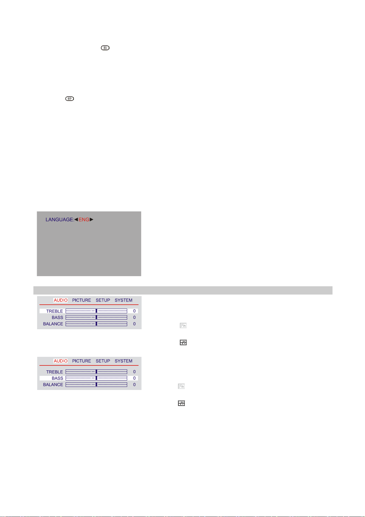
LANGUAGE
When you start using your set for the first time, you must select the language which
will be used for displaying menus and indications.
Press "←, →" (on remote control) button to select English, German, French, Spanish, or
Italian as your preferred OSD language.
AUDIO
TREBLE
1. Press "MENU" (on main body) or "►" (on remote
control) button.
2. Press " " (on main body) or "↑, ↓" (on remote
control) button to select TREBLE.
3. Press "
" (on main body) or "←, →" (on remote
control) button to lower or raise the treble for sound.
BASS
1.Press "MENU" (on main body) or "►" (on remote
control) button.
2.Press " " (on main body) or "↑, ↓" (on remote
control) button to select BASS.
3.Press " " (on main body) or "←, →" (on remote
control) button to lower or raise the bass for sound.
20
Page 21
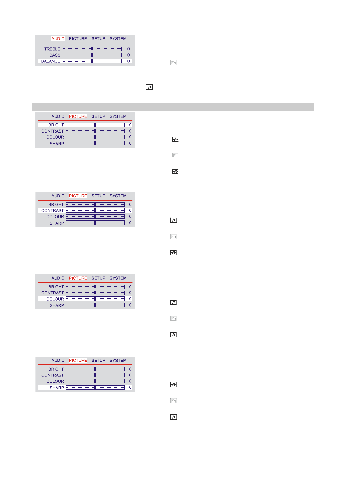
BALANCE
1.Press "MENU" (on main body) or "►" (on remote
control) button.
2.Press " " (on main body) or "↑, ↓" (on remote
control) button to select BALANCE.
3.Adjust the speaker balance on Left/Right by pressing "
" (on main body) or "←, →" (on remote control)
button.
PICTURE
BRIGHT
1. Press "MENU" (on main body) or "►" (on remote
control) button.
2. Press "
control) button to select PICTURE.
" (on main body) or "→" (on remote
3. Press " " (on main body) or "↑, ↓" (on remote
control) button to select BRIGHT.
4. Press " " (on main body) or "←, →" (on remote
control) button to increase or decrease the screen
brightness.
CONTRAST
1.Press "MENU" (on main body) or "►" (on remote
control) button.
2.Press " " (on main body) or "→" (on remote
control) button to select PICTURE.
3.Press " " (on main body) or "↑, ↓" (on remote
control) button to select CONTRAST.
4.Press " " (on main body) or "←, →" (on remote
control) button to increase or decrease the screen
contrast.
COLOUR
1.Press "MENU" (on main body) or "►" (on remote
control) button.
2.Press "
control) button to select PICTURE.
" (on main body) or "→" (on remote
3.Press " " (on main body) or "↑, ↓" (on remote
control) button to select COLOUR.
4.Press " " (on main body) or "←, →" (on remote
control) button to lower or higher the screen colour
intensity.
SHARP
1.Press "MENU" (on main body) or "►" (on remote
control) button.
2.Press " " (on main body) or "→" (on remote
control) button to select PICTURE.
3.Press " " (on main body) or "↑, ↓" (on remote
control) button to select SHARP.
4.Press " " (on main body) or "←, →" (on remote
control) button to adjust the contrast for soft or sharp.
21
Page 22

SETUP
CH. SEARCH
1. Press "MENU" (on main body) or "►" (on remote
control) button.
2. Press " " (on main body) or "→" (on remote
control) button to select SETUP.
3. Press " " (on main body) or "↑, ↓" (on remote
control) button to select CH. SEARCH.
4. Press " " (on main body) or "←, →" (on remote
control) button to select NO or YES. If you select YES,
the TV will scan program channels automatically.
CH. MEMORY
1. Press "MENU" (on main body) or "►" (on remote
control) button.
2. Press " " (on main body) or "→" (on remote
control) button to select SETUP.
3. Press " " (on main body) or "↑, ↓" (on remote
control) button to select CH. MEMORY.
4. Press " " (on main body) or "←, →" (on remote
control) button to select NO or YES. If you select
YES, the TV will add the you are currently watching
to the memory.
FINE TUNE
If the reception is clear, you do not have to fine-tune the
channel, as this is done automatically during the search
and store operation. If however the signal is weak or
distorted, you may have to fine-tune the channel
manually.
1. Press "MENU" (on main body) or "►" (on remote
control) button.
2. Press " " (on main body) or "→" (on remote
control) button to select SETUP.
3. Press “ “ (on main body) or “↑, ↓” (on remote
control) button to select FINE TUNE.
4. Press “ “ (on main body) or “←, →” (on remote
control) button to fine-tune the channel manually if the
reception is not very clear. You can increase or decrease
the number to achieve the best picture.
CH. SWAP
1. Press “MENU” (on main body) or “►” (on remote
control) button.
2. Press “ “ (on main body) or “→” (on remote
control) button to select SETUP.
3. Press “ “ (on main body) or “↑, ↓” (on remote
control) button to select CH. SWAP.
4. Press “
“ (on main body) or, press the appropriate
numbers on remote control to select the original
channel number you’d like to change.(eg 001).
5. Repeat the last operation to assign the target channel
number to the original channel.
22
Page 23

RECALL
1. Press “MENU” (on main body) or “►” (on remote
control) button.
2. Press “ “ (on main body) or “→” (on remote
control) button to select SETUP.
3. Press “ “ (on main body) or “↑, ↓” (on remote
control) button to select RECALL.
4. Press “ “ (on main body) or “←, →” (on remote
control) button to select NO or YES. If you select YES,
the TV will recall all the picture settings to default.
SYSTEM
1. Press “MENU” (on main body) or “►” (on remote
control) button.
2. Press “ “ (on main body) or “→” (on remote control)
button to select SETUP.
3. Press “ “ (on main body) or “↑, ↓” (on remote control)
button to select SYSTEM.
4. Press “ “ (on main body) or “←, →” (on remote
control) button to select OFF or ON. If you select
OFF, the SYSTEM menu will have no function when
you push the menu button. This menu is not normally
needed once you have tuned the set in for the first time.
To see the SYSTEM menu select ON in the SETUP
menu.
23
Page 24

SYSTEM
Please make sure the SYSTEM menu is ON status before selecting it. (Please refer to above
SYSTEM- OFF ON setting in the SETUP menu.)
PAL/SECAM/SECAM L
1.Press "MENU" (on main body) or "►" (on remote
control) button.
2.Press " " (on main body) or "→" (on remote
control) button to select SYSTEM.
3.Press " " (on main body) or "↑, ↓" (on remote
control) button to select PAL / SECAM / SECAM L.
4.Press "
" (on main body) or "←, →" (on remote
control) button to select the appropriate PICTURE
signal type from PAL, SECAM, and SECAM L.
SOUND
1.Press "MENU" (on main body) or "►" (on remote
control) button.
2.Press " " (on main body) or "→" (on remote
control) button to select SYSTEM.
3.Press " " (on main body) or "↑, ↓" (on remote
control) button to select SOUND.
4.Press " " (on main body) or "←, →" (on remote
control) button to select the appropriate sound system
from B/G, D/K, or I. The sound system will display on
top-righter coner of screen “B”, “D” or “I” of your
choice.
NICAM
1.Press "MENU" (on main body) or "►" (on remote
control) button.
2.Press " " (on main body) or "→" (on remote control)
button to select SYSTEM.
3.Press " " (on main body) or "↑, ↓" (on remote
control) button to select NICAM.
4.Press " " (on main body) or "←, →" (on remote
control) button to select ON or OFF. You can select ON
if your set is equipped with the receiver for NICAM
reception. The high quality NICAM (N
I
nstantaneous Companded Audio Multiplex)
ear
digital
sound can be received.
24
Page 25

3 VISUAL PERFORMANCE
3.1 MEASUREMENT CONDITIONS
Warm up time: 30min.
Angle for measurement:
Distance: 100cm
Equipment: Minolta CS-100
Measurement positions:
320
90°H and V
640 960
256
2 1
512 5
4 3
768
Grey scale definition: White means digital value for RGB=255,255,255
50% gray, RGB=127,127,127
Black, RGB=0,0,0
3.2 PICTURE SIZE AND CENTERING
3.2.1 SIZE CONTROL RANGE
The picture size can be adjusted to achieve activation of all pixels of the display in1280 X
For 1280 X 768 resolution the picture size is equal to the active area of the display. For
Smaller Resolution (SVGA, VGA Text and VGA Graphics) there is an expansion algorithm
which expands the picture to a maximum possible size. The display is centered with respect
to the front bezel opening with a tolerance of 0.5mm
25
Page 26

768 resolution
Resolution, for XGA, SVGA, VGA Text and VGA Graphics the conditions of 3.2 can be
met.
3.2.2 POSITION CONTROL RANGE
The picture position can be adjusted that a complete picture can be displayed centered
3.2.3 Max. BRIGHTNESS : PC Mode
340(MIN.), 400(Typ.) cd/m2
Test conditions: - center of display (5)
- video input (RGB) = 0.7Vpp
- brightness control is set to max.
- contrast control is set to max.
3.2.4 MIN. BRIGHTNESS : PC Mode
< 100 cd/m2
Test conditions: - center of display (5)
- video input (RGB) = 0.700V
- brightness control is set to min.
- contrast control is set to min..
3.2.5 CONTRAST RATIO : PC Mode
The contrast ratio(CR) measured at center position (5) of the display for it should be better
than 210(MIN.), 400(Typ.).
and is calculated according to the following formula.
Brightness of all pixels white
CR =
Brightness of all pixels black
3.3 BRIGHTNESS UNIFORMITY
The brightness uniformity has to be better than 70% and is calculated according to
to the following formula:
Ymin
With Y1 to Y5 as the brightness values with all pixels white at the 5 measurement positions
△Y = [
Ymax
] X 100%
3.4 WHITE COLOR COORDINATES
The white color temperature should be app. (CIE1931, Normal : 9300 and 6500),A 3th
channel should be available, which can be defined by the user. The measurement position is
the center of the display(5) at brightness set to maximum and Contrast set to center. The
tolerance of the color coordinates should be less than ± 0.020
26
Page 27

27
Page 28

3.5 WHITE COLOR UNIFORMITY
The deviation of the white color coordinates at the 4 positions (1)….(4) should not exceed
± 0.020 with respect to the measurement at the center position(5).
3.6 PURITY
Purity is defined as the uniformity of the chromaticity of the three primary colors. The
Deviation of the color coordinates of the primary colors red/green/blue at the 4 positions
(1)…(4) should not exceed ± 0.020 with respect to the measurement at the center position(5)
3.7 RESPONSE TIME
The response time of the display for Fujitsu should be better than 15ms typ. The response
time is measured from 90% to 10% (tr) and from 10% to 90% (tf) for a transition from white
(100%) to black (0%) to white (100%)
3.8 VIEWING ANGLE
Panel Horizontal view angle Vertical view angle at CR >10
Fujitsu 160 160
3.9 SURFACE TREATMENT OF FRONT POLARIZER
The front polarize should have hard coating (3H) and anti-glare treatment.
4. AUDIO Electrical Performance
4.1 STANDARD TESTING CONDITIONS :
4.1.1 Test Equipment ﹕ Audio Analyzer test equipment
4.1.2 Conditions of Input Signal
1). Input Impedance ﹕ 600 ohm
2). Input Level ﹕ 700m Vrms ± 10%
3). Signal Frequency ﹕ 1 KHz
28
Page 29

4.1.3 Ambient Temperature ﹕ 25℃± 5℃
4.1.4 Warm up Time ﹕ minimum 10 minutes after power on and audio signal input
4.1.5 Test Distance ﹕ 50cm from monitor screen and at the center of left and right speaker
4.1.6 Output Impedance ﹕ 4.5 ohm ± 15%
4.1.7 Output Voltage ﹕ Effective output state means standard testing conditions
29
Page 30

4.2 AMPLIFIER CHARACTERISTIC
4.2.1 Output Power ( Unit : Watt)
1). Effective Output ﹕ 2.5 Watts ( measure at the output voltage of 1% Distortion Factor)
2). Maximum Output ﹕ 3 Watts (measure at the output voltage of 20% Distortion Factor)
3). Measurement method
- Set Test Equipment
Meas ﹕ LEVEL , Freq ﹕ 1KHz
AMPTD ﹕ Vrms, HPF/LPF ﹕ OFF RANGE ﹕ AUTO
- Measure output voltage ( RMS)
- Output calculation formula ﹕ P=V2/R
V﹕ RMS value of output voltage P ﹕ Output Power R﹕ Speaker Impedance
4.3 SPEAKER CHARACTERISTIC :
4.3.1 Input ﹕ Normal 2.5 Watt
4.3.2 Impedance ﹕ 4.5 ohm ±15% ohm at 1KHz
4.3.3 Resonant Frequency ( f0)﹕150± 10% Hz
4.3.4 Frequency Range: 20Hz ~ 20KHz
30
Page 31

5 TUNER Electrical Performance
5.1.1 Receiving System : ( PAL STANDARD SYSTEM )
Channel VHF Low BAND : 48.25MHz ~ 160.00 MHz
High BAND : 160.00MHz ~ 442.00 MHz
UHF BAND : 442.00MHz ~863.25 MHz
Intermediate Frequency PIF : ( 38.90 )MHz
CIF : ( 34.47 )MHz
SIF : B/G: 33.40 MHz : 33.16 MHz
D/K: 32.40 MHz
I: 32.9 MHz
B/G, D/K: 33.05 MHz : I : 33.348 MHz
Input Impedance : UHF/VHF Terminal ( 75 ) Ohm, Unbalanced
Output Impedance : VIDEO : C.V.B.S
AUDIO : AF/MPX
IF : SECOND IF
Band Chang - Over System : ( PLL Control System )
Tuning System : ( Electronic Tuning System With PLL )
31
Page 32

(1) PAL B/G Air Channel
Channel Frequency
(Mhz)
2
3
4
5
6
7
8
9
10
11
12
21
22
23
24
25
26
27
28
29
30
31
32
33
34
35
36
37
38
39
40
41
42
43
44
45
46
47
48.25
55.25
62.25
175.25
182.25
189.25
196.25
203.25
210.25
217.25
224.25
471.25
479.25
487.25
495.25
503.25
511.25
519.25
527.25
535.25
543.25
551.25
559.25
567.25
575.25
583.25
591.25
599.25
607.25
615.25
623.25
631.25
639.25
647.25
655.25
663.25
671.25
679.25.
Channel Frequency
(Mhz)
48
49
50
51
52
53
54
55
56
57
58
59
60
61
62
63
64
65
66
67
68
69
687.25
695.25
703.25
711.25
719.25
727.25
735.25
743.25
751.25
759.25
767.25
775.25
783.25
791.25
799.25
807.25
815.25
823.25
831.25
839.25
847.25
855.25
32
Page 33

(2) PAL B/G Ca ble Chan n el
Channel Frequency
(Mhz)
2
3
4
5
6
7
8
9
10
11
12
13
14
15
16
17
18
19
20
21
22
23
24
25
26
27
28
29
30
31
32
33
34
35
36
37
38
48.25
55.25
62.25
69.25
76.25
83.25
90.25
97.25
105.25
112.25
119.25
126.25
133.25
140.25
147.25
154.25
161.25
168.25
175.25
182.25
189.25
196.25
203.25
210.25
217.25
224.25
231.25
238.25
245.25
252.25
259.25
266.25
273.25
280.25
287.25
294.25
303.25
Channel Frequency
(Mhz)
39
40
41
42
43
44
45
46
47
48
49
50
51
52
53
54
55
56
57
58
59
60
61
62
63
64
65
66
67
68
69
70
71
72
73
74
75
311.25
319.25
327.25
335.25
343.25
351.25
359.25
367.25
375.25
383.25
391.25
399.25
407.25
415.25
423.25
431.25
439.25
447.25
455.25
463.25
471.25
479.25
487.25
495.25
503.25
511.25
519.25
527.25
535.25
543.25
551.25
559.25
567.25
575.25
583.25
591.25
599.25
Channel Frequency
(Mhz)
76
77
78
79
80
81
82
83
84
85
86
87
88
89
90
91
92
93
94
95
96
97
98
99
100
101
102
103
104
105
106
107
607.25
615.25
623.25
631.25
639.25
647.25
655.25
663.25
671.25
679.25
687.25
695.25
703.25
711.25
719.25
727.25
735.25
743.25
751.25
759.25
767.25
775.25
783.25
791.25
799.25
807.25
815.25
823.25
831.25
839.25
847.25
855.25
33
Page 34

(3) PAL D/K Air Channel
Channel Frequency
(Mhz)
1
2
3
4
5
6
7
8
9
10
11
12
13
14
15
16
17
18
19
20
21
22
23
24
25
26
27
28
29
30
31
32
33
34
35
36
37
49.75
57.25
65.75
77.25
85.25
168.25
176.25
184.25
192.25
200.25
208.25
216.25
471.25
479.25
487.25
495.25
503.25
511.25
519.25
527.25
535.25
543.25
551.25
559.25
607.25
615.25
623.25
631.25
639.25
647.25
655.25
663.25
671.25
679.25
687.25
695.25
703.25
Channel Frequency
(Mhz)
38
39
40
41
42
43
44
45
46
47
48
49
50
51
52
53
54
55
56
57
711.25
719.25
727.25
735.25
743.25
751.25
759.25
767.25
775.25
783.25
791.25
799.25
807.25
815.25
823.25
831.25
839.25
847.25
855.25
863.25
34
Page 35

(4) PAL D/K Cable Channel
Channel Frequency
(Mhz)
1
2
3
4
5
6
7
8
9
10
11
12
13
14
15
16
17
18
19
20
21
22
23
24
25
26
27
28
29
30
31
32
33
34
35
36
37
49.75
57.75
65.75
77.25
85.25
112.25
120.25
128.25
136.25
144.25
152.25
160.25
168.25
176.25
184.25
192.25
200.25
208.25
216.25
224.25
232.25
240.25
248.25
256.25
264.25
272.25
280.25
288.25
296.25
304.25
312.25
320.25
328.25
336.25
344.25
352.25
360.25
Channel Frequency
(Mhz)
38
39
40
41
42
43
44
45
46
47
48
49
50
51
52
53
54
55
56
57
58
59
60
61
62
63
64
65
66
67
68
69
70
71
72
73
74
368.25
376.25
384.25
392.25
400.25
408.35
416.25
424.25
432.25
440.25
448.25
456.25
471.25
479.25
487.25
495.25
503.25
511.25
519.25
527.25
535.25
543.25
551.25
559.25
567.25
575.25
583.25
591.25
599.25
607.25
615.25
623.25
631.25
639.25
647.25
655.25
663.25
Channel Frequency
(Mhz)
75
76
77
78
79
80
81
82
83
84
85
86
87
88
89
90
91
92
93
94
95
96
97
98
99
671.25
679.25
687.25
695.25
703.25
711.25
719.25
727.25
735.25
743.25
751.25
759.25
767.25
775.25
783.25
791.25
799.25
807.25
815.25
823.25
831.25
839.25
847.25
855.25
863.25
35
Page 36

(5) PAL I Air Channel
Channel Frequency
(Mhz)
1
2
3
4
5
6
7
8
9
21
22
23
24
25
26
27
28
29
30
31
32
33
34
35
36
37
38
39
40
41
42
43
44
45
46
47
48
45.75
53.75
61.75
175.25
183.25
191.25
199.25
207.25
215.25
471.25
479.25
487.25
495.25
503.25
511.25
519.25
527.25
535.25
543.25
551.25
559.25
567.25
575.25
583.25
591.25
599.25
607.25
615.25
623.25
631.25
639.25
647.25
655.25
663.25
671.25
679.25
687.25
Channel Frequency
(Mhz)
49
50
51
52
53
54
55
56
57
58
59
60
61
62
63
64
65
66
67
68
69
695.25
703.25
711.25
719.25
727.25
735.25
743.25
751.25
759.25
767.25
775.25
783.25
791.25
799.25
807.25
815.25
823.25
831.25
839.25
847.25
855.25
36
Page 37

(6) PAL I Cable Channel
Channel Frequency
(Mhz)
1
2
3
4
5
6
7
8
9
10
11
12
13
14
15
16
17
18
19
20
21
22
23
24
25
26
27
28
29
30
31
32
33
34
35
36
37
38
105.25
112.25
119.25
126.25
133.25
140.25
147.25
154.25
161.25
168.25
175.25
182.25
189.25
196.25
203.25
210.25
217.25
224.25
231.25
238.25
245.25
252.25
259.25
266.25
273.25
280.25
287.25
294.25
303.25
311.25
45.75
53.75
61.75
69.25
76.25
83.25
90.25
97.25
Channel Frequency
(Mhz)
39
40
41
42
43
44
45
46
47
48
49
50
51
52
53
54
55
56
57
58
59
60
61
62
63
64
65
66
67
68
69
70
71
72
73
74
75
76
319.25
327.25
335.25
343.25
351.25
359.25
367.25
375.25
383.25
391.25
399.25
407.25
415.25
423.25
431.25
439.25
447.25
455.25
463.25
471.25
479.25
487.25
495.25
503.25
511.25
519.25
527.25
535.25
543.25
551.25
559.25
567.25
575.25
583.25
591.25
599.25
607.25
615.25
Channel Frequency
(Mhz)
77
78
79
80
81
82
83
84
85
86
87
88
89
90
91
92
93
94
95
96
97
98
99
100
101
102
103
104
105
106
107
623.25
631.25
639.25
647.25
655.25
663.25
671.25
679.25
687.25
695.25
703.25
711.25
719.25
727.25
735.25
743.25
751.25
759.25
767.25
775.25
783.25
791.25
799.25
807.25
815.25
823.25
831.25
839.25
847.25
855.25
863.25
37
Page 38

(7) SECAM L´ Air Channel
Channel Frequency
(Mhz)
1
2
3
4
5
6
7
8
9
10
21
22
23
24
25
26
27
28
29
30
31
32
33
34
35
36
37
38
39
40
41
42
43
44
45
46
47
48
47.75
55.75
60.5
63.75
176
184
192
200
208
216
471.25
479.25
487.25
495.25
503.25
511.25
519.25
527.25
535.25
543.25
551.25
559.25
567.25
575.25
583.25
591.25
599.25
607.25
615.25
623.25
631.25
639.25
647.25
655.25
663.25
671.25
679.25
687.25
Channel
49
50
51
52
53
54
55
56
57
58
59
60
61
62
63
64
65
66
67
68
69
Frequeny
(Mhz)
695.25
703.25
711.25
719.25
727.25
735.25
743.25
751.25
759.25
767.25
775.25
783.25
791.25
799.25
807.25
815.25
823.25
831.25
839.25
847.25
855.25
38
Page 39

6 ACCESSORIES
6.1 POWER CABLE
Length : 1.8m + 5cm/-5cm
Color : black
Connectors : Monitor–side / Mains-side : IEC 320-1 / CEE7-VII (EU)
: IEC 320-1 / BS-1363 (UK)
6.2 EXTERNAL ADAPTER
Type : Worldwide type
Length of DC cable : 1.5m + 1.5cm/-0cm
Color of adapter : black
Connectors : Monitor-side
: Mains-side : IEC 320 male
: Φ2.5mm DC plug
6.3 REMOTE CONTROL & BATTERIES
Remote Control : 35 keys
Battery : 1.5V AAA x 2 pcs
39
Page 40

7 ENVIRONMENTAL
7.1 ENVIRONMENTAL CONDITIONS (CLIMATIC)
Operation (according to IEC 721 / EN 60721 Class 3K3) : (unpacked for a long time)
Temperature
Humidity 20% ~ 85%
Max. Dew Point Temperature
Max. abs. Air Humidity 25 g/m3
Max. change of Temperature
Height 3000m
Air pressure 700~1060 mbar (70~10Kpa)
Dewing Not allowed
Storage (according to IEC 721 / EN 60721 Class 1K2): (unpacked for a long time)
Temperature
Relative Humidity 5% ~ 85%
Absolute Air Humidity 1 ~ 25 g/m3
+5°C ~ + 40°C
+27°C
0.5°C/min
-10°C ~ + 50°C
Air pressure 700~1060 mbar (70~106Kpa)
Radiation Solar heat 700 W/m2
Max. Change of Temperature
0.5°C/min. (max. 10°C/30min.)
40
Page 41

7.2 ENVIRONMENTAL CONDITION (MECHANICAL)
Storage and Transport: (according to IEC 721 / EN 60721 class 2M2)
Test Procedure
IEC 68/EN 60068
Vibration Freq. range Hz 5~10 10~100 100~500
(random vibration) Change db/oct +12
-6
Spectral
IEC 68-2-64 acceleration m2/s3 0.75
EN 60068-2-64 density
Accel. RMS m/s2 11.4
Axis - 3
Duration/Axis Minutes 30
Free fall Weight kg
Fall height m 0.9 0.76
ISO 2248
EN 22248
Underground concrete
Direction and number 1 time on 1 corner, 3 edge,
0~9.1 9.1~18.2
18.2~27.2
0.61
6 surface
8 MECHANICAL REQUIREMENTS
8.1 VIBRATION AND SHOCK
All testing shall be done in each of three mutually perpendicular axes, referenced to the position of
the system as it is in front of the user (i.e., front-to back, side-to-side, and top-to-bottom).
8.1.1 Non-Operating
The unit should suffer minimal visible cosmetic damage or damage that presents a safety hazard, or
impairs the setup and operation of the system after testing.
Sinusoidal Vibration: 0.75 G zero-to-peak, 10 to 500Hz, 0.5 octave / minute sweep rate. This
requires one sweep, 10 to 500 to 10Hz, along each of the three axes.
Random Vibration: 0.008 G2/Hz, 10 to 500 Hz, nominal 2 GRMS. The test shall be for one hour
for each of the three axes.
Half Sine Wave Shock: 120 G peak, half sine pulse, 2 ms pulse duration. Testing shall consist of
one shock in each direction in each axis, for a total of 6 shock inputs.
Square Wave Shock: 40 G peak acceleration, 160 inches / second velocity change. There shall be
one shock in each direction in each axis, for a total of 6 shock inputs.
41
Page 42

8.2 PACKAGE DROP SPECIFICATION
Listed below are standards of drop heights for monitor product
Product Weight height Specs
<9.1 kg 0.91 m
9.2~18.2 kg 0.76 m
18.3~27.2 Kg 0.61 m
27.3~45.4 Kg 0.46 m
8.2.1 Drop Test Sequence
Drop Order Drop point Drop Times
1 Right Front Bottom Corner 1
2 Right Bottom Edge 1
3 Right Front Edge 1
4 Front Bottom Edge 1
5 Bottom Side 1
6 Top Side 1
7 Front Side 1
8 Back Side 1
9 Left Side 1
10 Right Side 1
8.3 DIMENSION SIZE AND WEIGHT
Dimension size 518 (W) x 333 (H) x 198 (D)
Net Weight 5.0 Kg + 0.3kg
Gross Weight 6.8 Kg + 0.3kg
42
Page 43

8.4 GAP SPEC.
8.4.1 The step between front bezel and back cover shall be within specification.
Back Cover & Bezel Gap Neck Front & Neck Back
1.0mm ≤ A ≤ 1.4mm 1.0mm ≤ C ≤ 1.4mm
Back Cover & Bezel Alignment
0 mm ≤ B ≤ 0.5mm
Back Cover & Tuner Door
0.8 mm ≤ D ≤ 1.2mm
LV171-E06
LV171-E07
43
Page 44

Back Cover & Tuner Door
0.8 mm ≤ E ≤ 1.2 mm
Back Cover & Key Plate
0.6 mm ≤ F ≤ 1.2 mm
LV171-E08
LV171-E09
44
Page 45

8.4.2 LCD Horizontally
The angle between front bezel and LCD unit in bottom side should be not large than 1.0mm.
LV171-E10
The distance G-H of the LCD display unit from left side to right should be not large than 4.0mm.
LV171-E11
Tilt Base Rotation
Tilt up 25 ± 2°/ down 5 ± 2°
45
Page 46

8.5 PLASTIC MATERIAL
Front Bezel ABS 94HB, 94V-0
Back Cover ABS 94HB, 94V-0
The Others ABS 94HB
8.6 GAP SPEC.
Gap between panel with bezel is 0.2 mm < gap < 1.5 mm
46
Page 47

9 Block
9.1 MAIN BOARD BLOCK DIAGRAM
47
Page 48

9.2 TUNER BOARD BLOCK DIAGRAM
48
Page 49

10 Connect
10.1 PCBA CONNECTOR LOCATION
10.1.1 K701-DM
10.1.2 R701-DM
10.1.3 VTV-N7910
49
Page 50

50
10.1.4 VTV-VL7021D-M
Page 51

10.2 CONNECTOR P/N ASSIGNMENT
10.2.1 CONNECTOR Function
Location Function Type
CN101 VGA I/P D-sub 15P Female -A
CN201/CN552 Remote control 5P Housing
CN202/CN550 KEY pad control 8P Housing
CN1/CN654 Inverter PW I/P 13P Housing
CN653/CN801 Tuner IN connector D-sub 15P M/Female -R
CN301/CN652 Tuner I/P 6P wire
CN651 S-Video I/P 4 Pin Mini-DIN female
CN650 Component I/P RCA female(G, B, R)
CN655 Composite I/P RCA female(Y, W, R)
CN656 Component audio I/P RCA female(W, R)
CN401 Speaker L 2P Housing
CN402 Speaker R 3P Housing
CN601 Panel ODD O/P 40P Housing
CN602 Panel EVEN O/P 30P Housing
JZ1 PC Audio I/P 3P Wafer
CN2 Power I/P 2P Wafer
51
Page 52

10.2.2 CONNECTOR PIN ASSIGNMENT
Location\
PIN
CN101 R-IN G-IN B-IN
CN201/
CN552
CN202/
CN550
CN1/
CN654
CN653/
CN801
CN301/
CN652
CN651 GND GND
CN650 GND
CN655 GND
CN656 GND
CN401 LFSPEAK GND
CN402 RFSPEAK NC GND
CN601
CN602
1 2 3 4 5 6 7 8 9 10 11 12 13 14 15
ISP-
GND GND GND GND
SCL
PWR- G PWR-
OSDS7
5V 5V GND GND GND
TVAVOUT
VHS-2
REF.
Schematic
REF.
Schematic
Y
OSD-
S6
PWTV
TVAVOUT
AU1R
COMPCr
AU2R
5V GND
OSDS5
TVLOUT
GND
SLUM
GND AU1-L GND
GND
GND
IRDAT
OSD-
OSD-
S4
S3
TV-
GND GND MSDA
ROUT
TV-
GND
ROUT
S-
CHR
COMP-
GND
Cb
AU2-
L
OSD-
OSD-
S2
S0
PAN-
PAN-
ON
BRI
TVLOUT
AV-
CVBS
COMPY
ISP-
DDC
DET.
5V
GND
12V 12V 12V
MTS-
VHS2
MODE MSCL
SU
DDC
PCRIN
DDCSDA
PCLIN
MTSST
Hsync Vsync
GND
MTSMA
DDCSCL
5V 12V
53
Page 53

Appendix A: PCBA Assembly
54
Page 54

5
4
3
2
1
+5V
L501
HI0805N310
C502
C501
+
0.1U
47U/16V
D D
RSTP5
ALEP5
/INT0P5
/WRP5
/RDP5
UCLKP5
C C
VSOUT
R512 NC C536
VS2
R513 0
OSC1P5
HSOUTP8
SOGOUTP8
VSOUTP8
VS2P8
CLAMP_VGAP8
SCL_AP8
SDA_AP8
B B
VLLCP3
VHSP3,6
VVSP3
EXVCLKP8
A A
OSC1
HSOUT
SOGOUT
VSOUT
VS2
CLAMP_VGA
SCL_A
SDA_A
VLLC
VHS
VVS
EXVCLK
C524
27p-NC
R515
1M-NC
C525
27p-NC
4
VS_IN
VS_IN
U502
LT1117-2.5 V
SOT_223
RST
ALE
/INT0
/WR
/RD
UCLK
X501
14.318MHz
5
+2.5V_VP +3.3V
3
IN
OUT
ADJ
2
1
R511 10
C523
27p-NC
R501
NC
R502
0
UCLKOUT
C503
+
47U/16V
VD[0..7]P3
AD[0..7]P5
AR[0..7]P8
AG[0..7]P8
AB[0..7]P8
+2.5V_VP
+2.5V_VP
HI0805N310
HI0805N310
HI0805N310
L502
+2.5V_VP
Chip Interfac e
CVDD
C505
C504
+
100U/16V
L503
L504
0.1U
AVDD2 PVDD
+
C512
47U/16V
GNDA2
AVDD1
+
C514
47U/16V
GNDA1
VD0
143
VD1
144
VD2
145
VD3
146
VD4
147
VD5
148
VD6
149
VD7
150
RST
151
ALE
137
/INT0
140
/WR
139
/RD
138
UCLKOUT
136
AD0
133
AD1
132
AD2
131
AD3
130
AD4
129
AD5
128
AD6
127
AD7
126
AR0
207
AR1
208
AR2
AR3
AR4
AR5
AR6
AR7
AG0
185
AG1
186
AG2
187
AG3
188
AG4
189
AG5
190
AG6
191
AG7
192
AB0
166
AB1
167
AB2
168
AB3
169
AB4
170
AB5
171
AB6
172
AB7
173
198
199
200
201
202
203
204
205
175
176
177
178
179
180
181
182
HSOUT
VS_IN
193
194
196
195
SCL_A
SDA_A
CLAMP_VGA
VHS
163
VVS
VLLC
EXVCLK
OSC1
XTALO
GNDA1
162
161
165
164
156
153
154
SOGOUT
PWM_BRI
GNDA2
GNDA1
1
2
3
4
5
6
8
9
10
11
12
13
14
15
18
19
20
21
17
C507
C506
0.1U
0.1U
C513
0.1U
C515
0.1U
RA0/VD0
RA1/VD1
RA2/VD2
RA3/VD3
RA4/VD4
RA5/VD5
RA6/VD6
RA7/VD7
RESET
ALE
INT
WR*
RD*
UCLK
AD0
AD1
AD2
AD3
AD4
AD5
AD6
AD7
AR0
AR1
AR2
AR3
AR4
AR5
AR6
AR7
AG0
AG1
AG2
AG3
AG4
AG5
AG6
AG7
AB0
AB1
AB2
AB3
AB4
AB5
AB6
AB7
BR0/V0
BR1/V1
BR2/V2
BR3/V3
BR4/V4
BR5/V5
BR6/V7
BR7/V7
BG0/U0/UV0
BG1/U1/UV1
BG2/U2/UV2
BG3/U3/UV3
BG4/U4/UV4
BG5/U5/UV5
BG6/U6/UV6
BG7/U7/UV7
BB0/Y0/VD0
BB1/Y1/VD1
BB2/Y2/VD2
BB3/Y3/VD3
BB4/Y4/VD4
BB5/Y5/VD5
BB6/Y6/VD6
BB7/Y7/VD7
AHSYNC
AVSYNC
DHS/VHS1
DVS/VVS1
DCLK/VLLC1
DDE/FIELD1
SCL
SDA
COAST
VHS0
VVS0
PWM1/SOGIN
PWM2/FIELD0
VLLC0
EXVCLK
XTALI/OSC
XTALO
GNDA2
4
C508
0.1U
152
155
AVDD1
AVSS1
157
160164297134
MSDA
AVDD2
AVSS2
MSCL
158
159222389142
C509
0.1U
C511
C510
0.1U
0.1U
C516
C517
0.1U
0.1U
GNDM
GNDM
C518
C519
RAS*
CAS*
GNDP
UVDD
C522
0.1U
MD0
MD1
MD2
MD3
MD4
MD5
MD6
MD7
MD8
MD9
WE*
CKE
P28
P29
P32
P33
P34
P35
P36
P37
P40
P41
P42
P43
P44
P45
C520
0.1U
0.1U
GNDP GNDP
MD0
40
MD1
39
MD2
38
MD3
37
MD4
36
MD5
35
MD6
34
MD7
33
MD8
31
MD9
30
MD10
29
MD11
28
MD12
27
MD13
26
MD14
25
MD15
24
MA0
60
MA1
59
MA2
58
MA3
57
MA4
56
MA5
55
MA6
54
MA7
53
MA8
52
MA9
51
MA10
50
MA11
49
/RAS
45
/CAS
44
/WE
43
CKE
46
MCLKOUT
47
A1BLU0
63
A1BLU1
64
A1BLU2
65
A1BLU3
66
A1BLU4
67
A1BLU5
68
A1BLU6
69
A1BLU7
70
A1GRN0
72
A1GRN1
73
A1GRN2
74
A1GRN3
75
A1GRN4
76
A1GRN5
77
A1GRN6
78
A1GRN7
79
A1RED0
81
A1RED1
82
A1RED2
83
A1RED3
84
A1RED4
85
A1RED5
86
A1RED6
87
A1RED7
88
B1BLU0
99
B1BLU1
100
B1BLU2
101
B1BLU3
102
B1BLU4
103
B1BLU5
104
B1BLU6
105
B1BLU7
106
B1GRN0
108
B1GRN1
109
B1GRN2
110
B1GRN3
111
B1GRN4
112
B1GRN5
113
B1GRN6
114
B1GRN7
115
B1RED0
117
B1RED1
118
B1RED2
119
B1RED3
120
B1RED4
121
B1RED5
122
B1RED6
123
B1RED7
124
PCLK
90
PVS
92
PHS
93
PPDE
94
FPVCC
96
PAN_ON
95
PW_TV
62
DAC_BRI
125
U501
TP6760
Scaler
PQFP 208-Pin 0.5mm
0.1U
GNDP
184
183741618098116
135
UVDD
PVDD1
PVDD2
CVDD1
CVDD2
CVDD3
CVSS1
CVSS2
CVSS3
PVDD3
CVDD4
CVDD5
DVDD1
DVDD2
MVDD1
MVDD2
MD10
MD11
MD12
MD13
MD14
MD15
TSP1/MA0
TREV1/MA1
TGPO0/MA2
TGPO1/MA3
TGPO2/MA4
TGPO3/MA5
TGPO4/MA6
TGPO5/MA7
TGPO6/MA8
TGPO7/MA9
TGPO8/MA10
TGPO9/MA11
TCLK1/MCLK
PB2/P0
PB3/P1
PB4/P2
PB5/P3
PB6/P4
PB7/P5
PB8/P6
PB9/P7
PG2/P8
PG3/P9
PG4/P10
PG5/P11
PG6/P12
PG7/P13
PG8/P14
PG9/P15
PR2/P16
PR3/P17
PR4/P18
PR5/P19
PR6/P20
PR7/P21
PR8/P22
PR9/P23
CSN0/P24
CSN1/P25
DISP/P26
PARITY/P27
PB0/P30
PB1/P31
PG0/P38
PG1/P39
PR0/P46
PR1/P47
TCLK0/SHFCLK
PVSYNC
TREV0/PHSYNC
TSP0/PDE
FPVCC
FPBACK
DVD0
DVD1
CVSS4
CVSS5
DVSS1
DVSS2
MVSS1
MVSS2
PVSS1
PVSS2
PVSS3
174
20632487191
GNDM
GNDP
UVSS
107
141
197
L505
DVDD
HI0805N310
L506
MVDD
HI0805N310
C521
+
47U/16V
+5V
L511
HI0805N310
option for Panel
System Configuration Setting
R504/505/506 (MA0,1,2) : Sel Panel Type
R509 (MA6) : FPVCC Polarity
R510 (MA7) : FPBACK Polarity
R504 10K
R505 10K
R506 10K
R509 NC
R510 NC
MCLKOUT MCLK
PCLK
PHS
PPDE
DAC_BRI
PWM_BRI
C541
0.1U
L507
NC
L508
HI0805N310
GNDP
3
C539
.01U
+3.3V
+5V
<+5V>
+3.3V
<+3.3V>
option
R503
22
GNDM
R514
22
C527
27p-NC
GNDP
L517
FBM-L10-160808-300LMT
GNDP
L514
FBM-L10-160808-300LMT
GNDP
L515
FBM-L10-160808-300LMT
GNDP
R507 1K
R508 1K-NC
C540
47U/16V
C526
10p
C528
10p
C529
10p
C530
10p
C531
10p
A1BLU0
A1BLU1
A1BLU2
Memory Configuration
+3.3V
C532
+
47U/16V
U503
SDRAM_1MX16
MA0
21
A0
MA1
22
A1
MA2
23
A2
MA3
24
A3
MA4 MD4
27
A4
MA5
28
A5
MA6
29
A6
MA7
30
A7
MA8
31
A8
MA9
32
A9
MA10
20
A10
MA11
19
/RAS
/CAS
/WE
MCLK
GNDM
SHFCLK
PVSYNCPVS
PHSYNC
PDE
PAN_BRI
+
Power Plane : +2.5V_VP,CVDD,PVDD,MVDD
Power Line : AVDD1,AVDD2,DVDD,UVDD
Ground Plane : GND,GNDP,GNDM
Ground Line : GNDA1,GNDA2
A11
17
RAS
16
CAS
15
W
18
CS
14
DQML
36
DQMU
26 1
VSS VCC
50 25
VSS VCC
4
VSSQ
10
VSSQ
41
VSSQ
47
VSSQ
+3.3V_MC
C534
C533
0.1U
0.1U
GNDM
Power Plane : +3.3_MQ
Power Line : +3.3V _MC
Ground Plane: GNDM
2
L509
HI0805N310
L510
HI0805N310
D0
D1
D2
D3
D4
D5
D6
D7
D8
D9
D10
D11
D12
D13
D14
D15CLK
CKE
NC
NC
VCCQ
VCCQ
VCCQ
VCCQ
+3.3V_MQ
C535
0.1U
GNDM
0.1U
2
3
5
6
8
9
11
12
39
40
42
43
45
46
48
4935
34
33
37
7
13
38
44
+3.3V_MC
+3.3V_MQ
MD0
MD1
MD2
MD3
MD5
MD6
MD7
MD8
MD9
MD10
MD11
MD12
MD13
MD14
MD15
CKE
+3.3V_MC
C537
0.1U
+3.3V_MQ
C538
0.1U
A1BLU3
A1BLU4
A1BLU5
A1BLU6
A1BLU7
A1GRN0
A1GRN1
A1GRN2
A1GRN3
A1GRN4
A1GRN5
A1GRN6
A1GRN7
A1RED0
A1RED1
A1RED2
A1RED3
A1RED4
A1RED5
A1RED6
A1RED7
B1BLU0
B1BLU1
B1BLU2
B1BLU3
B1BLU4
B1BLU5
B1BLU6
B1BLU7
B1GRN0
B1GRN1
B1GRN2
B1GRN3
B1GRN4
B1GRN5
B1GRN6
B1GRN7
B1RED0
B1RED1
B1RED2
B1RED3
B1RED4
B1RED5
B1RED6
B1RED7
SHFCLK
PVSYNC
PHSYNC
PDE
FPVCC
PAN_ON
PW_TV
PAN_BRI
Title
SCHEMATIC, CTRL/B VTV-L702,SLV87E
Size Document Number Rev
C
401AB0
Date: Sheet
SHFCLK P4
PVSYNC P4
PHSYNC P4
PDE P4
FPVCC P4
PAN_ON P6
PW_TV P3,6
PAN_BRI P5,6
A1BLU[0..7] P4
A1GRN[0..7] P4
A1RED[0..7] P4
B1BLU[0..7] P4
B1GRN[0..7] P4
B1RED[0..7] P4
1
2 9Friday, December 05, 2003
of
1C
Page 55

5
4
3
2
1
+5V
L301
HI0805N310
CN301
VIDEO-11P
1
2
3
PW_TVP2,6
R306 18
R307 18
R308 18
R309 18
R314 18
R315 18
R316 18
4
5
6
7
8
9
10
11
GNDV
R317
56
GNDV
G-TEXT
B-TEXT
R-TEXT
D
C C
AV1_TV_COM
AV1_RCA_COM
AV1_S_LUM
AV1_S_CHR
Y_IN
Cb_IN
Cr_IN
B B
MODE00
MODE02
A A
MODE07 S_VIDEO
MODE2E
AV1_RCA_COM
AV1_S_CHR
AV1_S_LUM
AV1_TV_COM
R310
56
Y_IN_B
Cb_IN_B
Cr_IN_B
R318
R319
56
56
TUNER
COMP.
Y Cb Cr
Cr_IN
Y_IN
Cb_IN
3V3B1
R331
4.7K
SAA_TV
SAA_RCA
SAA_LUM
SAA_CHR
R312
R311
56
56
GNDV
C341 0.047U
C342 0.047U
C343 0.047U
C344 0.047U
C346 0.047U
C347 0.047U
C348 0.047U
R303
4.7K-NC
MSCL
R304 33
MSDA
R305 33
C323 0.047U
C324 0.047U
C325 0.047U
C326 0.047U
R313
56
A13
A23
A33
A43
A24
A34
A44
C321
33p
C322
33p
A14
A21
A12
A22
GNDV
VHS_O
VVS_O
C301
47U/16V
X301
24.576MHZ
R320 0-NC
C327 0.047U
R346 0-NC
C328 0.047U
R322 0-NC
R323 0-NC
R324 0-NC
C329 0.047U
R325 0-NC
R326 0-NC
R327 0-NC
C340 0.047U
R338 0-NC
+
C302
0.1U
A12
A13
A21
A22
A23
A33
A43
XCLKXCLK1
U301
3
IN
OUT
ADJ
LT1117 - 3 . 3V
A3
XTAL
B4
XTALI
N4
CE
N9
SCL
P10
SDA
C6
TRSTN
J2
AI11
K1
AI12
K2
AI13
L3
AI14
K3
AI1D
G4
AI21
G3
AI22
H2
AI23
J3
AI24
H1
AI2D
E3
AI31
F2
AI32
F3
AI33
G1
AI34
F1
AI3D
B1
AI41
D2
AI42
D1
AI43
E1
AI44
D3
AI4D
B5
TDI
B6
TCK
D6
TMS
A7
XCLK
B7
XDQ
C7
XRH
D8
XRV
XRDY
B11
XTRI
N6
CLKEXT
P3
EXMCLR
2
1
4
A11 XCLK1
A14
A24
A34
A44
GNDV
VSSE1
D5D9D11
3V3B1
C5C9D12
VSSE2
R301
NC
C303
100U/16V
R302
0
VDDE1
VDDE2
VSSE3
VSSE4
G11L4L8
VDDE3
VSSE5
H12M4M8
VDDE4
VSSE6
+3.3V_SAA
VDDE5
VSSE7
L11D7D10
+
M11C8C10
F12
J12M5M9M3K4L1H4J1F4G2D4
VDDI1
VDDI2
VDDI3
VDDI4
VDDE6
VSSI1
VDDI5
VDDE7
VSSI2
VSSI3
VSSI4
VSSI5
VSSI6
F11
J11L5L9M2J4H3E4C1C2
GNDV
L302
HI0805N310
C304
100U/16V
L303
HI0805N310
C313
100U/16V
B3
VXDD
VDDI6
SAA7118
VSSA0
VSSA1
VSSA2
Power Plane : 3V3A1,3V3B1
Power Line : +3.3V_SAA
Ground Plane : GNDV
5
4
VDDA0
VDDA1
U302
VSSA3
VSSA4
3V3B1
C306
0.1U
C315
0.1U
C308
C307
0.1U
0.1U
C316
C317
0.1U
0.1U
P13
D13
C14
A13
B12
TEST0
TEST1
TEST2
TEST3
TEST4
XTOUT
TDO
INT_A
FSW
M13
ASCLK
AMCLK
A2A6A5
P9
N11
P11
R335
0-NC
C305
+
0.1U
3V3A1
C314
+
0.1U
GNDV
3V3A1
E2
VDDA2
VDDA3
VDDA4
VDDA1A
VDDA2A
VDDA3A
VDDA4A
AGND
AGNDA
VXSS
L2
A4
FBLK
R334
NC
3
C309
0.1U
C318
0.1U
A12
TEST5
AMXCLK
M12
ALRCLK
P12
C310
0.1U
C319
0.1U
R336
4.7K-NC
ICLK
IDQ
IGPH
IGPV
IGP0
IGP1
ITRDY
ITRI
IPD0
IPD1
IPD2
IPD3
IPD4
IPD5
IPD6
IPD7
HPD0
HPD1
HPD2
HPD3
HPD4
HPD5
HPD6
HPD7
XPD0
XPD1
XPD2
XPD3
XPD4
XPD5
XPD6
XPD7
ADP0
ADP1
ADP2
ADP3
ADP4
ADP5
ADP6
ADP7
ADP8
LLC
LLC2
AOUT
RTCO
RTS0
RTS1
RESON
3V3B1
C311
0.1U
C320
0.1U
R337
0-NC
C312
M14
L13
K12
K14
L14
K13
N12
L12
G14
G12
H11
H14
H13
J14
J13
K11
D14
E11
E13
E12
E14
F13
F14
G13
A8
B8
A9
B9
A10
B10
A11
C11
N8
P8
M7
L7
P7
N7
L6
M6
P6
P4
N5
M1
L10
M10
N10
P5
0.1U
RP301
33 *4
RP302
33 *4
VVS_O
VHS_O
753 1
753 1
RTS0
RTS1
2
VD0
VD1
VD2
VD3
86 42
VD4
VD5
VD6
VD7
8 642
AOUT
R339 0
R340 0
R333 0
R332 0
AOUT
THS
TVS
FBLK
R-TEXT
G-TEXT
B-TEXT
MSCL
MSDA
VHS
VVS
VLLC
AOUT P9
THS P9
TVS P9
FBLK P9
R-TEXT P9
G-TEXT P9
B-TEXT P9
MSCL P5,6,7,8,9
MSDA P5,6,7,8,9
VHS P2,6
VVS P2
VLLC P2
XCLK1P9
VD[0..7] P2
4:2:2
L305
FBM-L10-160808-300LMT
R328 75
R341
0-NC
R342
0-NC
Title
SCHEMATIC, CTRL/B VTV-L702,SLV87E
Size Document Number Rev
A3
Date: Sheet
THS
TVS
VVS
VHS
401AB0
GNDV
VLLCAV1_CLK1
C345
NC
3 9Friday, December 05, 2003
1
1C
of
D
Page 56

5
LP601
B1BLU[0..7]P2
D
B1BLU7
B1BLU6
B1BLU5
B1BLU4
33 *4
81
7
2
6
3
54
3
2
8 1
7
6
5 4
B2BLU7
B2BLU6
B2BLU5
B2BLU4
CP601
33p *4
A1BLU[0..7]P2
4
LP603
33 *4
A1BLU7
A1BLU6
A1BLU5
A1BLU4
81
7
2
6
3
54
5 4
A2BLU7
A2BLU6
A2BLU5
A2BLU4
3
2
CP603
33p *4
8 1
7
6
3
LP605
B1RED[0..7]P2 A1RED[0..7]P2
B1RED7
B1RED6
B1RED5
B1RED4
33 *4
81
7
2
6
3
54
5 4
2
B2RED7
B2RED6
B2RED5
B2RED4
3
2
CP605
33p *4
8 1
7
6
A1RED7
A1RED6
A1RED5
A1RED4
1
LP607
33 *4
81
7
2
6
3
54
5 4
A2RED7
A2RED6
A2RED5
A2RED4
3
2
CP607
33p *4
8 1
7
6
D
81
7
6
54
4039
3837
36
FPVCC P2
SHFCLK P2
PVSYNC P2
PHSYNC P2
PDE P2
5 4
GNDP
GNDPGNDP
3
6
GNDP
PDE
PVSYNC
1
2
7
A2RED6
A2RED4
A2RED2
A2GRN6
A2GRN4
A2GRN2A2GRN3
A2GRN0
A2BLU6
A2BLU4
A2BLU2
A2BLU0
4 9Friday, December 05, 2003
8 1
A2RED3
A2RED2
A2RED1
A2RED0
CP608
33p *4
+
GNDP
of
PANEL VCC
C602
47U/16V
1C
LP602
33 *4
B1BLU3
B1BLU2
2
B1BLU1
3
B1BLU0
C C
LP609
B1GRN[0..7]P2
B B
A A
B1GRN7
B1GRN6
B1GRN5
B1GRN4
B1GRN3
B1GRN2
B1GRN1
B1GRN0
33 *4
2
3
LP610
33 *4
2
3
5
GNDP
5 4
5 4
3
6
GNDP
GNDP
GNDP
B2BLU3
B2BLU2
B2BLU1
B2BLU0
2
CP602
33p *4
8 1
7
B2GRN7
B2GRN6
B2GRN5
B2GRN4
3
2
CP609
33p *4
8 1
7
6
B2GRN3
B2GRN2
B2GRN1
B2GRN0
3
2
CP610
33p *4
8 1
7
6
FPVCC 0 ON
1 OFF
FPVCC
PANELVCC
R602
10K
L603
L11-321611-800
A1GRN[0..7]P2
option for Pane l
<+5V> <+3.3V>
B
E
GNDP
4
L601
L11-321611-800
Q601
PMBT3904
B
SOT
23
E
+5V
81
7
6
54
5 4
81
7
6
54
81
7
6
54
LP604
33 *4
A1BLU3
A1BLU2
2
A1BLU1
3
A1BLU0
A1GRN7
A1GRN6
A1GRN5
A1GRN4
A1GRN3
A1GRN2
A1GRN1
A1GRN0
L602
NC
R601
47K
C
C
U601
SI9933
45
G2D2
36
S2D2
27
G1D1
18
S1D1
MAGEPOWER SOIC-8
2
3
2
3
81
7
6
54
LP611
33 *4
LP612
33 *4
+3.3V
GNDP
A2BLU3
A2BLU2
A2BLU1
A2BLU0
3
2
CP604
33p *4
8 1
7
6
5 4
GNDP
3
6
GNDP
3
6
A2GRN7
A2GRN6
A2GRN5
A2GRN4
2
CP611
33p *4
8 1
7
A2GRN3
A2GRN2
A2GRN1
A2GRN0
2
CP612
33p *4
8 1
7
81
7
6
54
5 4
81
7
6
54
5 4
B2RED7
B2RED5
B2RED3
B2RED1
B2GRN7
B2GRN5
B2GRN3
B2GRN1
B2BLU7
B2BLU5
B2BLU3
B2BLU1
B1RED3
B1RED2
B1RED1
B1RED0
LP606
33 *4
81
7
2
6
3
54
CN602
29 30
29 30
27 28
27 28
25 26
25 26
23 24
23 24
21 22
21 22
19 20
19 20
17 18
17 18
15 16
15 16
13 14
13 14
11 12
11 12
9 10
91 0
7 8
78
5 6
56
3 4
34
1 2
12
GNDP GNDP
15*2 SMD
LCD Panel Connector
125MDD-30DT 15*2Pin 1.25mm
3
6
5 4
GNDP
B2RED6
B2RED4
B2RED2
B2RED0
B2GRN6
B2GRN4
B2GRN2
B2GRN0
B2BLU6
B2BLU4
B2BLU2
B2BLU0
B2RED3
B2RED2
B2RED1
B2RED0
2
CP606
33p *4
8 1
7
PHSYNC
PANEL VCC
GNDP
SHFCLK
A2RED7
A2RED5
A2RED3
C601
+
A2RED1 A2RED0
47U/16V
A2GRN7
A2GRN5
A2GRN1
A2BLU7
A2BLU5
A2BLU3
A2BLU1
GNDP
LP608
33 *4
A1RED3
A1RED2
2
A1RED1
3
A1RED0
CN601
35
35
33 34
33 34
31 32
31 32
29 30
29 30
27 28
27 28
25 26
25 26
23 24
23 24
21 22
21 22
19 20
19 20
17 18
17 18
15 16
15 16
13 14
13 14
11 12
11 12
9 10
91 0
7 8
78
5 6
56
3 4
34
1 2
12
20*2 SMD
LCD Panel Connector
125MDD-40DT 20*2Pin 1.25mm
FPVCC
SHFCLK
PVSYNC
PHSYNC
PDE
4039
3837
36
Power Line : PANELVCC
GNDP
Title
Size Document Number Rev
3
2
Date: Sheet
Ground Plane : GNDP
SCHEMATIC, CTRL/B VTV-L702,SLV87E
A3
401AB0
Page 57

5
R553
10K
+5V
(SOURCE )
(POWER)
(OSD)
(UP)
(DOWN)
(+)
(-)
C550
0.1U
EA/VP
UCLK
UCLK2
RST
/INT0
IR_DAT
MUTE_S
OSD_S0
OSD_S7
OSD_S6
OSD_S5
OSD_S4
OSD_S3
OSD_S2
C551
27p-NC
R550
1M-NC
RST
C552
27p-NC
+5V
+
MSDAP3,6,7,8,9
PAN_BRIP2,6
D D
C C
UCLK
X550
14.318MHz-NC
UCLK2
+5V
C553
10U/16V
R551
1K
PAN_BRI
R552
10K
MSCL
MSDA
MSCL /WR
MSDA
Keypad interface
C557
CN550
KEY BD
1
B B
2
3
4
5
6
7
8
C556
.01U
.01U
C558
.01U
C559
.01U
C560
.01U
C561
.01U
C562
.01U
Remote control interface
+5V
IR_DAT
MPU_G
MPU_Y
C564
NC
R554 510
R555 510
C565
NC
1
2
3
4
5
CN552
IR BD
A A
C567
5
C566
.01U
NC
PWR_G
PWR_Y
35
21
20
10
14
15
16
17
12
R558
4.7K
R559
4.7K
4
+5V
U550
SM59264
RP550
47K *4
75 3 1
B
E
B
E
MPU
GND VCC
22 44
OSD_S7
OSD_S6
OSD_S5
OSD_S4
OSD_S3
OSD_S2
OSD_S0
753 1
RP551
47K *4
Q551
PMBT3904
B
SOT
23
E
Q552
PMBT3904
B
SOT
23
E
8 642
C
C
P0.0
P0.1
P0.2
P0.3
P0.4
P0.5
P0.6
P0.7
P2.0
P2.1
P2.2
P2.3
P2.4
P2.5
P2.6
P2.7
WR
PSEN
ALE/P
TXD
RXD
C
C
RD
NC
NC
864 2
EA/VP
X1
X2
RESET
INT0
INT1
T0
T1
2
P1.0
3
P1.1
4
P1.2
5
P1.3
6
P1.4
7
P1.5
8
P1.6
9
P1.7
1
NC
NC
4
AD0
43
AD1
42
AD2
41
AD3
40
AD4
39
38
37
36
24
25
26
27
28
29
30
31
19
18
32
33
13
11
23
34
PWR_G
PWR_Y
+5V
+5V
R561
AD5
AD6
10K
AD7
MPU_Y
MPU_G
DSUB_DET D_DET
MCU_BRI PAN_BRI
/RD
/WR
ALE
TXD
RXD
+5V
R556
510
+5V
R557
510
R562 0
R567 1K-NC
C554
R560
10K
100p
+5V
3
+5V
C555
0.1U
1 8
A0 VCC
2 7
A1 WP
3 6
A2 SCL
4 5
GND SDA
U551
24C16
Debug port
+5V
RXD
TXD
3
CN551
NC
1
2
3
4
Debug port
Pitch 2.54mm
+5V
MSCL
MSDA
Debug port (IIC)
+5V
MSCL
MSDA
UCLK2
2
AD0
AD1
AD2
AD3
AD4
AD5
AD6
AD7
R568 0-NC
CN553
NC
1
2
3
4
IIC Debug
Pitch 2.54mm
2
1
AD[0..7] P2
MUTE_S
D_DET
RST
ALE
/INT0
/RD
UCLK
Title
Size Document Number Rev
B
Date: Sheet
MUTE_S P7
D_DET P8
RST P2
ALE P2
/INT0 P2
/WR P2MSCLP3,6,7,8,9
/RD P2
UCLK P2
OSC1P2
L552
HI0805N310
GNDPGNDM
L551
HI0805N310
GND_AO
Power Plane : +5V
Ground Plane : GND
SCHEMATIC, CTRL/B VTV-L702,SLV87E
401AB0
5 9Friday, December 05, 2003
1
of
1C
Page 58

5
4
3
2
1
TUNER OUT Connector
CN655
CONN DSUB 25-R
0-NC
+3.3V
MSDA
MSCL
AU1_L
AU1_R
AU2_L
AU2_R
TV_LOUT
TV_ROUT
+9V_ADO
+5V
VHS
GND_AI
D D
+5V +12V1
L654
F32B-332
CN654
POWER BD-13P
Pitch 2.0mm
C C
1
2
3
4
5
6
7
8
9
10
11
12
13
GND_AI
+5V
L653
B B
L11-321611- 800
C650
47U/16V
+
PAN_ON
PAN_BRI
PC_RIN
PC_LIN
C652
0.1U
L655
F32D-471
U650
LT1084-3.3V
4
POWER SAVE CONTROL +12V
+12V1
IN
OUT
ADJ
PW_TV
PW_TV
1 ON
3
2
1
R653 10K
+12V
R650
NC
R651
0
B
E
+3.3V1
+
C651
100U/16V
Q650
PMBT3904
B
SOT
23
E
U651
SI9933
C
C
C654
.01U
R652
47K
45
G2D2
36
S2D2
27
G1D1
18
S1D1
L659
L11-321611- 800
C653
0.1U
R654
1
1
2
2
3
3
4
4
5
5
6
6
7
7
8
8
9
9
10
10
11
11
12
12
13
13
CN650
VIDEO-11P
1
2
3
4
5
6
7
8
9
10
11
14
14
15
15
16
16
17
17
18
18
19
19
20
20
21
21
22
22
23
23
24
24
25
25
AV-CVBS1
AV_CHR
AV_LUM
TV_CVBS
GNDV
GNDV
GNDV
GND_AI
Cr
Y
Cb
Cr
Y
Cb
AV-CVBS1
AV_CHR
AV_LUM
R657 0
R655 39 / 2W-NC
R656 39 / 2W-NC
TV_CVBS
+12V+12VT
VHS
+9V_ADO
AU1_L
AU1_R
AU2_L
AU2_R
PC_RIN
PC_LIN
TV_LOUT
TV_ROUT
MSDA
MSCL
PAN_ON
PW_TV
PAN_BRI
VHS P2,3
+9V_ADOP7
AU1_L
P7
AU1_R P7
AU2_L
P7
AU2_R P7
PC_RIN
P7
PC_LIN
P7
TV_LOUT
P7
TV_ROUT
P7
MSDA P3,5,7,8,9
MSCL P3,5,7,8,9
PAN_ON P2
PW_TV P2,3
PAN_BRI P2,5
+5V
VCC
VDD
A A
G84D
G84P GND_AIGNDPGNDA1 GNDV
5
GNDA2G84A GND_AOGNDM
*Short these ground p lanes on PCB
Ground Line : GNDAM,GNDTV
GNDV
Title
SCHEMATIC, CTRL/B VTV-L702,SLV87E
Size Document Number Rev
B
4
3
2
Date: Sheet
401AB0
6 9Friday, December 05, 2003
1
of
1C
Page 59

5
GND_AI
R402
R401
2.2K
D D
AU1_RP6
AU1_LP6
AU1_L
2.2K
+
C401 2.2U
+
C402 2.2U
R403 2.4K
R404 2.4K
GND_AI
R419
R420
2.2K
2.2K
+
AU2_RP6
C C
AU2_LP6
AU2_R
AU2_L
C436 2.2U
C437 2.2U
+
R422 2.4K
R423 2.4K
GND_AI
R429
R430
2.2K
2.2K
+
GND_AI
C403 2.2U
C404 2.2U
C431 2.2U
C432 2.2U
R416
2.2K
TV_ROUTP6
TV_LOUTP6
B B
PC_RINP6
PC_LINP6
TV_ROUT
TV_LOUT
PC_RIN
PC_LIN
R415
2.2K
GND_AI
+
+
+
R405 2.4K
R406 2.4K
R414 2.4K
R421 2.4K
AVSV_RAU1_R
AVSV_L
AV2_R
AV2_L
TV_R
TV_L
+9V_ADO
PC_R
PC_L
4
L401
HI0805N310
TV_R
TV_L
AVSV_R
AVSV_L
AV2_R
AV2_L
PC_R
PC_L
MSDA
MSCL
C405
0.1U
GND_AI GND_AI
U401
PT2314
11
16
10
15
9
14
8
13
25
26
27
1
2
C438 4.7U/50V
C439 4.7U/50V
L404
L11-321611- 800
C433
47U/16V
RIN1
LIN1
RIN2
LIN2
RIN3
LIN3
RIN4
LIN4
DGND
DATA
CLK
VDD_A
AGND
+
+
+
C434
0.1U
OUT_R
OUT_L
LOUT
ROUT
BIN_R
BOUT_R
BIN_L
BOUT_L
TREB_L
TREB_R
LOUD_R
LOUD_L
REF
RIN
3
RFOUT1
23
LFOUT1
24
17
LIN
18
5
6
21
22
19
20
3
4
7
12
28
+
C406 2.2U
+
C407 2.2U
C410 2700p
C411 2700p
C412 0.1U
C413 0.1U
+
C416
47U/16V
RO1LFOUT1
R425
33K 1%
GND_AI
R407
5.6K
C408
C409
0.1U
0.1U
C414
C415
0.1U
0.1U
R408
5.6K
GND_AI
GND_AI
LFOUT
R427
1.69k 1%.1.87k 1% for Hitachi
GND_AO
GND_AI
LO1RFOUT1
R426
33K 1%
RFOUT
R428
1.69k 1%.1.87k for Hitachi
GND_AI
MUTE_S
100U/16V
LFOUT
RFOUT
C424
47U/16V
C420
+
2
C417
1000U/16V
C419
10U/16V
GND_AO
R409
10K
R410
120 1%
+
C421 10U/16V
C422 10U/16V
+
R411
C423
120 1%
100U/16V
GND_AO
+
+
+
GND_AO
1
L402 NC
L403 L11-321611- 800
+9V_ADO
+12V
AU_VCC
STBY
NF1
IN1
IN2
NF2
FILTER
PGND
GND1
GND2
4
Vcc
R424
3.3/3W fuse for Hitachi
U403
BA5417
1
NC
2
BS2
3
OUT2
5
OUT1
6
BS1
100U/16V
LFSPEAK
C425
100U/16V
+
+
C429
C426
470U/10V
R412
C428
470U/10V
+
R413
2.2
+
RFSPEAK
C427
0.15U
2.2
GND_AO
LFSPEAK
C430
0.15U
GND_AO
CN401
1
2
C418
+
0.1U
8
10
11
12
13
9
7
14
15
L-SPEAK-2P
RFSPEAK
CN402
1
2
3
R-SPEAK-3P
GND_AO
+9V_ADO+12V
+9V_ADO
MSDA
MSCL
MUTE_S
+9V_ADOP6
MSDA P3,5,6,8,9
MSCL P3,5,6,8,9
MUTE_S P5
4
U402
OUT
ADJ
LT1117
SOT_223
3
IN
2
R417
110
+
C435
47U/16V
1
R418
680
GND_AO
A A
PC_RIN
PC_LIN
ZD407 5.1V-NC
ZD408 5.1V-NC
ZD401 5.1V-NC
ZD402 5.1V-NC
Power Line : +9V_ADO,+9V_AUI,+9V_AUO
Ground Plane : GND_AI,GND_AO
Title
GND_AI
5
4
3
2
SCHEMATIC, CTRL/B VTV-L702,SLV87E
Size Document Number Rev
B
Date: Sheet
401AB0
7 9Friday, December 05, 2003
1
of
1C
Page 60

5
+5V
L101
HI0805N310
C101
+
47U/16V
C102
0.1U
D
U101
LT1117-3.3V
3
IN
4
2
OUT
1
ADJ
AD9883 PLL
G84P
R101
NC
R102
0
+
C103
47U/16V
L102
HI0805N310
+3.3V_AP
+3.3V
G84D
C152
0.1U
4
L105
HI0805N310
+3.3V_VD
+3.3V_AP
C125
0.082U
C126
8200p
R123 2.2K
C128
C127
1000p
0.1U
G84P
3
R124 300
R125 300
CLAMP_VGA
C129
1000p
C130
0.1U
G84D
R126 0
R127
NC
VS_VGA
HS_VGA
2
RP101
DV0
DV1
DV2
DV3
DV4
DV5
DV6
DV7
100 *4
753 1
RP102
100 *4
75 3 1
AR0
AR1
AR2
AR3
864 2
AR4
AR5
AR6
AR7
86 42
1
AR[0..7] P2
D
+5V
L103
HI0805N310
C104
+
47U/16V
CLAMP_VGAP2
C C
SCL_AP2
B B
A A
SOGOUT
VS2P2
SDA_AP2
HSOUT
EXVCLK
VSOUT
D_DET
VS2
VS_VGA
HS_VGA
C105
0.1U
CLAMP_VGA
MSDAP3,5,6,7,9
MSCLP3,5,6,7,9
VS2
SCL_A
SDA_A
P2
P2
P2
P2
P5
U105D
74F14
4
AD9883 AD
MSDA
MSCL
HSOUT
EXVCLK
SOGOUT
VSOUT
D_DET
U105A
12
74F14
U105B
34
74F14
98
U105F
1312
74F14
5
U102
LT1117 - 3.3 V
IN
OUT
ADJ
R131 NC
3
2
1
+5V
U105C
74F14
U105E
74F14
BLUE
GREEN
RED
DATACLK
C107
0.1U
L104
HI0805N310
R103
NC
R104
0
G84A
R105 0
R106 0
R107 0
L110
FBM-L10-160808-300LMT
R128
75 C124
56
SCL_A
1110
C108
NC
DET.D_DET
C106
+
47U/16V
R115
R117 75
R118 75
C109
NC
G84A
G84A
SDA_A
+3.3V_AD
C137
0.1U
C141
0.1U
G84A
C144
0.1U
75-NC
G84A
C138
1000p
C142
1000p
MSCL
MSDA
C146
G84A
+5V_DDC
R111
10K
SCL
VSYNC
R119 75-NC
R129 75
4
0.047U
R108 75
R109 75
22p
R113
10K
HSYNC
C136
+5V
C139
0.047U
C140
1000p
C143
0.047U
C145
0.1U
EXVCLK
R112
10K
G84D
30293231333635
COAST
HSYNC
Red.4
Red.5
DV4
DV5
+3.3V_VD
Red.3
DV3
282227
GND
Red.2
DV2
C133
1000p
VD
Red.0
Red.1
77767574737271
DV0
DV1
C149
1000p
R120 75 1%
242625
GNDVDGND
VDD
VDD
80
79
78
G84D
R121
R122 75 1%
VDD
VDD
GND
Blue.0
Blue.1
Blue.2
Blue.3
Blue.4
Blue.5
Blue.6
Blue.7
VDD
GND
Green.0
Green.1
Green.2
Green.3
Green.4
Green.5
Green.6
Green.7
GND
GND
C150
0.1U
75 1%
C134
0.1U
+3.3V_VD
214323
GND
+3.3V_VD
+5V
U106
AD9883-140M
20
19
18
17
16
15
14
13
12
11
10
9
8
7
6
5
4
3
2
1
D102
EC10QS04
D101
EC10QS04
47U/16V
GREENG
RED
C131
C132
0.1U
0.1U
G84A
+3.3V_AD
+3.3V_AD
41
R130
NC
DET.
42
44
45
46
47
48
49
50
51
52
53
54
55
56
57
59
60
+3.3V_AD
15
10
14
9
13
8
12
7
6
C135
0.1U
G84A
+5V_DDC+5V
+5V
R114
10K
SDA
40
GND
GND
VD
BAIN
GND
VD
VD
GND
GAIN
SONGIN
GND
VD
VD
GND
RAIN
A0
SCL
SDA
Ref Bypass
VD
GND
GND
61
G84A
VGA In
CN101
DB15-3_FEMALE
5
4
3
2
111
16
17
G84AG84A
393738
VD
34
PVD
PVD
FILT
GND
CLAMP
MIDSCV
GND
VSYNC
AD9883
VDD
VSOUT
GND
VD
63
62
C147
0.1U
C120
NC
GND
SOGOUT
DATACK
HSOUT
64
655867
66
VSOUT
SOGOUT
DATACLK
HSOUT
B BLUE
R
C121
NC
Red.6
Red.7
69
68
70
DV7
DV6
C148
0.1U
G84D
L107 FBM-L10-160808-300LMT
L108 FBM-L10-160808-300LMT
L109 FBM-L10-160808-300LMT
C122
NC
G84A
3
DV16
DV17
DV18
DV19
DV20
DV21
DV22
DV23
DV8
DV9
DV10
DV11
DV12
DV13
DV14
DV15
C123
+
G84D
+3.3V_VD
C151
0.1U
+5V_DDC
0.1U
2
DV8
DV9
DV10
DV11
DV12
DV13
DV14
DV15
DV16
DV17
DV18
DV19
DV20
DV21
DV22
DV23
U107
1 8
A0 VCC
2 7
A1 WP
3 6
A2 SCL
4 5
GND SDA
24C21A
DDC EDID Data
RP103
100 *4
753 1
RP104
100 *4
753 1
RP105
100 *4
753 1
RP106
100 *4
75 3 1
Title
Size Document Number Rev
A3
Date: Sheet
AG0
AG1
AG2
AG3
8642
AG4
AG5
AG6
AG7
864 2
AB0
AB1
AB2
AB3
864 2
AB4
AB5
AB6
AB7
86 42
1
G84A G84A G84
VS1 VS2
R116
SCL
SDA
SCHEMATIC, CTRL/B VTV-L702,SLV87E
AG[0..7] P2
AB[0..7] P2
R
3
D103
BAV99
2
+5V +5V+5V
0
1
SCL
SDA
VSYNC
HSYNC
DET.
401AB0
1
G
3
D104
BAV99
2
ZD101 5.1V
ZD102 5.1V
ZD103 5.1V
ZD104 5.1V
ZD105 5.1V-NC
8 9Friday, December 05, 2003
B
3
D105
BAV99
2
1
A
G84A
of
1C
Page 61

5
4
3
2
1
+5V +3.3V_VDA
L450
HI0805N310
3
OUT
ADJ
U450
LT1117-3.3V
R454
10K
GDA
TSCL
TSDA
IN
2
1
R455
10K
R473 100
R474 100
R456
0
+
C450
D D
C
+5V
47U/16V
L453 HI0805N310
C457 47U/16V-NC
+
C451
0.1U
4
+5V_T
C459 0.1U
1 8
A0 VCC
2 7
A1 WP
3 6
A2 SCL
4 5
GND SDA
U451
AOUT
24C16
C460 0.1U
B
GDA
A
L455
HI0805N310-NC
GDCGDA
5
R450
NC
R451
0
GDC
GDA
C461
0.1U
GDAGDA GDA
L451
HI0805N310
L452
HI0805N310
+
C452
47U/16V
C455
47U/16V
+3.3V_VDC
GDC
1
P2.0/PWM
2
P2.0/PWM0
3
P2.2/PWM1
4
P2.3/PWM2
5
P2.4/PWM3
6
P2.5/PWM4
7
P2.6/PWM5
8
P2.7/PWM6
9
P3.0/ADC0
10
P3.1/ADC1
11
P3.2/ADC2
12
P3.3/ADC3
13
VSSC
14
SCL(NVRAM)
15
SDA(NVRAM)
16
P0.2
17
P0.3
18
P0.4
19
P0.5
20
P0.6
21
P0.7
22
VSSA
23
CVBS0
24
CVBS1
25
SYNC_FILTER
26 27
IREF FRAME
U452
R457
SAA5264
24K
4
VDDP
RESET
XTALOUT
XTALIN
OSCGND
VDDC
VSSP
VSYNC
HSYNC
VDDA
P3.4/PWM7
COR
TEST
+
P1.5
P1.4
SDA
SCL
P1.3
P1.2
P1.1
P1.0
VDS
AOUT
THS
TVS
FBLK
C456
0.1U
C453
47U/16V
+
C454
0.1U
+3.3V_VDA
B-TEXT
GDA
52
RES.
51
50
49
R470 0
R471 0
MSDA
MSCL
R472
10K
C464
+
10U/16V
D451
1N4148-NC
G-TEXT
R-TEXT
MSDA
MSCL
48
47
46
GDA
XCLK1
AOUT P3
THS P3
TVS P3
FBLK
B-TEXT
G-TEXT
R-TEXT
P3
P3
P3
P3
MSDA P3,5,6,7,8
MSCL P3,5,6,7,8
XCLK1 P3
45
44
43
+3.3V_VDA
RES.
R469 0
VDSFBLK
42
41
C462
22p
X450
12MHz
C463
22p
40
39
+3.3V_VDC
38
R476
150
TVS
THS
VDS
R477
150
GDA
R-TEXT
G-TEXT
B-TEXT
37
36
35
34
R
33
G
32
B
31
30
GDA
+3.3V_VDA
R464 0
R463 0
R462 0
R461 0
R460 0
R459 0
R475
150
U453
1
R'D0
2
D0
3
CP0
4
S'D0
5
Q0
6
Q'0
7
GND
VCC
R'D1
CP1
S'D1
Q1
Q'1
D1
74F74/NC
+5V
14
13
12
11
10
9
8
R466 NC
R465 NC
VDS
XCLK1
FBLK
29
28
GDAGDAGDA
GDA
R458
0-NC
GDA
3
Title
SCHEMATIC, CTRL/B VTV-L702,SLV87E
Size Document Number Rev
A4
Date: Sheet
2
401AB0
of
9 9Friday, December 05, 2003
1
1C
C
B
A
Page 62

5
D D
4
3
2
1
OSD_S0 OSD_S2
S201
KSM0632B
C C
OSD_S3
S202
KSM0632B
OSD_S4 OSD_S6
S203
KSM0632B
OSD_S5
S204
KSM0632B
S205
KSM0632B
OSD_S7
S206
KSM0632B
S207
KSM0632B
Plu sMin us OSDFunction PowerChannelSource
B B
CN202
VT4501-08
1
2
3
4
5
6
7
8
OSD_S7
OSD_S6
OSD_S5
OSD_S4
OSD_S3
OSD_S2
OSD_S0
A A
Title
SCHEMATIC, KEY/B VTV-K701,SLV87E
Size Document Number Rev
A
5
4
3
Date: Sheet
2
404AB0
of
2 2Tuesday, June 17, 2003
1
1A
Page 63

5
D D
3
2
1
C202
2.2U/16V
C C
+
U201
RIM-B38
+5V
4
R202
100
IR_DAT
R201
47K
C201
1000P
3
2
123
D201
LYG2093 YEL/GRN
1
PWR_GPWR_Y
IR Receiver
CN201
VA4301-05
B B
A A
1
2
3
4
5
PWR_G
PWR_Y
IR_DAT
+5V
Title
SCHEMATIC, IRKEY/B VTV-R701,SLV87E
Size Document Number Rev
A
5
4
3
Date: Sheet
2
404AB1 1A
of
2 2Tuesday, June 17, 2003
1
Page 64

5
ANT1
ANTENNA
D D
SLAVE ADDRESS = C0
TV_AVO UT TV_CVBS
S_CHR AV_CHR
C C
S_LUM
AV_CVBS
COMP_Y Y
COMP_Cb
COMP_Cr
B B
TUNER IN Connector
MSDA
MSCL
AU1_L
AU1_R
AU2_L
AU2_R
TV_LOUT
TV_ROUT
A A
+9V_ADO
+5V
VHS_IN
Tuner
T801
ANT
19 2
ANT VT
15
GND
16
GND
17
GND
18
GND
GNDTi
TUNER FQ1216
L808
FBM-L10-300
L809
FBM-L10-300
L810
FBM-L10-300
L811
FBM-L10-300
L812
FBM-L10-300
L813
FBM-L10-300
L814
FBM-L10-300
CN801
CONN DSUB 25-R
1
1
2
2
3
3
4
4
5
5
6
6
7
7
8
8
9
9
10
10
11
11
12
12
13
13
1
AGC
VS
SCL
SDA
AS
NC
NC
2IF
CVBS
VIF
AF
14
14
15
15
16
16
17
17
18
18
19
19
20
20
21
21
22
22
23
23
24
24
25
25
5
+5V_VS
3
MSCL
4
MSDA
5
6
9
10
11
12
13
14
C808
0.022U-NC
GNDAM GNDTi GNDAM
AV_LUM
AV_CVBS1
AV_CVBS1
AV_CHR
AV_LUM
+12VT
TV_CVBS
2IF
CVBS
+5V_VIF
MPX
C806
0.1U
Cb
Cr
Cr
Y
Cb
GNDTi
R801
+12VT
RCA
75
-NC
C802
0.1U
GNDTi
R802
0
C805
NC
GNDTi
NC
R805
R820
10 / 3W
R803
10 / 3W
47U/16V
MPX
MTS_L
MTS_R
COMP_Y COMP_Cb COMP_Cr AV_CVBS AU1_L AU1_R AU2_L AU2_R S_CHR S_LUM
CN804
RCA
R809 0-NC
R810 0-NC
R812 0
R813 0
C811
CN805
RCA
+
GNDTi
C807
47P-NC
GNDTi
+9V_ADO
R814
NC
+
4
C801
47U/16V
TV_AVOUT
U801
LT1 117-5V
+12VA
TV_LOUT
TV_ROUT
CN806
RCA
4
C812
0.1U
ADJ
1
CN807
RCA
3
+5VTuner
L801
BLM21P300S
R847 for hitachi
GNDAM
GNDAM
+5VTuner
3
D803
BAV99
2
CN810
RCA
0
C826
R846
0.01U
NC
R848 for hitachi
0
R849
NC
C804
+
47U/16V
3
1
3
GNDAM
C830
0.01U
D804
BAV99
2
GNDAM
C833
0.1U
L802
BLM21P300S
C803
+
47U/16V
GNDTi
4
OUT
IN
3
2
R804
NC
R806
0
3
D801
BAV99
2
1
+5V +5V+5V +5V +5V +5V
CN808
RCA
MTS_L
MTS_R
+5V
R808
NC
C813
0.1U
COMP_Cb COMP_CrCOMP_Y AV_CVBS S_CHR S_LUM
3
D802
BAV99
2
1
CN809
RCA
1
C823
47U/16V
DG
C845
NC
3
1
4 3
6 5
D805
BAV99
2
CN802
S-VIDEO
3
1
+
4443424140393837363534
1
OUTL
2
OUTR
3
VDDA1
4
VSSA1
5
VSSD1
6
VDDD1
7
VSSD2
8
NC1
9
TP2
10
NICAM
11
TP1
1213141516171819202122
24.576MHz
X801
C846
NC
GNDAMDGGNDAM
D806
BAV99
2
12
2
C817
NC
33
P2
P1
OUTM
VSSA4
U803
TDA9874AH
PCLK
ADDR1
XTALO
VREF2
XTALI
R833
8K2
EXTIL
EXTIR
TP3
TEST2
DG DG
SCK
VSSD3
VDDD3
32
SYSCLK
MONOIN
WS
31
SDO
30
SDAT
29
SCLK
28
VDDA3
27
VSSA3
26
CRST
25
SIF1
24
VREF1
23
SIF2
IREF
ADDR2
VSSA2
VDEC
TEST1
C840
0.47U
GNDAM GNDAM GNDAM GNDAM
SLAVE ADDRESS = 0XB0,0XB1
AU1_L
AU1_R
AU2_L
AU2_R
AU1_L
AU1_R
AU2_L
AU2_R
SC803
Screw Pad
SC801
Screw Pad
SC802
Screw Pad
0
0
0
L815 FBM-L10-300
L816 FBM-L10-300
L817 FBM-L10-300
L818 FBM-L10-300
ZD801 5.1V-NC
ZD803 5.1V-NC
ZD805 5.1V-NC
ZD807 5.1V-NCCN803
Title
Size Document Number Rev
B
2
Date: Sheet
SCHEMATIC, TUNER/B VTV-N7910,SLV87E
C821
0.1U
DG DG
C827
0.1U
C835
1U
DG
C814 1000p
C815 1000p
C816 1000p
C818 1000p
ZD802 5.1V-NC
ZD804 5.1V-NC
ZD806 5.1V-NC
ZD808 5.1V-NC
1
R815 10
R821 10
R824 10
R825 10
C828
0.1U
C831
47pF
C832
NC
C837
R831
0.1U
NC
405A99 1D
BLM21P300S
+
+
GNDAMGNDAMGNDAM
R827 22
R828 22
R829 0
R830 NC
R832
51
L804
BLM21P300S
BLM21P300S-NC
1
C822
47U/16V
BLM21P300S
C825
47U/16V
L821
L822
L807
3 3Tuesday, December 16, 2003
MSDA
MSCL
+5V
2IF
GNDAMDGGNDTi
of
L805
BLM21P300S
Page 65

312
13
010
016
2pcs
304
036
4pcs
023
VTV-R701
355
015
6pcs
356
018
307
21
025
3
003
007
020
4pcs
013
4pcs
VTV-L701
351
0
354
014
303
023
031
2pcs
028
301
029
034
035
026
4
001
017
2pcs
024
310
305
021
03
Page 66

THE UPDATED PARTS LIST
FOR THIS MODEL IS
AVAILABLE ON ESTA
Page 67

Hitachi, Ltd. Tokyo, Japan
International Sales Division
THE HITACHI ATAGO BUILDING,
No. 15 –12 Nishi Shinbashi, 2 – Chome,
Minato – Ku, Tokyo 105-8430, Japan.
Tel: 03 35022111
HITACHI EUROPE LTD,
Whitebrook Park
Lower Cookham Road
Maidenhead
Berkshire
SL6 8YA
UNITED KINGDOM
Tel: 01628 643000
Fax: 01628 643400
Email: consumer-service@hitachi-eu.com
HITACHI EUROPE GmbH
Munich Office
Dornacher Strasse 3
D-85622 Feldkirchen bei München
GERMANY
Tel: +49-89-991 80-0
Fax: +49-89-991 80-224
Hotline: +49-180-551 25 51 (12ct/min)
Email: HSE-DUS.service@hitachi-eu.com
HITACHI EUROPE srl
Via Tommaso Gulli N.39, 20147
Milano, Italia
ITALY
Tel: +39 02 487861
Tel: +39 02 38073415 Servizio Clienti
Fax: +39 02 48786381/2
Email: customerservice.italy@hitachi-eu.com
HITACHI EUROPE S.A.S
Lyon Office
B.P. 45, 69671 BRON CEDEX
FRANCE
Tel: 04 72 14 29 70
Fax: 04 72 14 29 99
Email: france.consommateur@hitachi-eu.com
HITACH EUROPE AB
Egebækgård
Egebækvej 98
DK-2850 Nærum
DENMARK
Tel: +45 43 43 6050
Fax: +45 43 60 51
Email: csgnor@hitachi-eu.com
Hitachi Europe Ltd
Bergensesteenweg 421
1600 Sint-Pieters-Leeuw
BELGIUM
Tel: +32 2 363 99 01
Fax: +32 2 363 99 00
Email: sofie.van.bom@hitachi-eu.com
www.hitachidigitalmedia.com
HITACHI EUROPE S.A.
364 Kifissias Ave. & 1, Delfon Str.
152 33 Chalandri
Athens
GREECE
Tel: 1-6837200
Fax: 1-6835964
Email: service.hellas@hitachi-eu.com
HITACHI EUROPE S.A.
Gran Via Carlos III, 86, planta 5
Edificios Trade - Torre Este
08028 Barcelona
SPAIN
Tel: 93 409 2550
Fax: 93 491 3513
Email: atencion.cliente@hitachi-eu.com
HITACHI Europe AB
Box 77 S-164 94 Kista
SWEDEN
Tel: +46 (0) 8 562 711 00
Fax: +46 (0) 8 562 711 13
Email: csgswe@hitachi-eu.com
HITACHI EUROPE LTD (Norway) AB
STRANDVEIEN 18
1366 Lysaker
NORWAY
Tel: 67 5190 30
Fax: 67 5190 32
Email: csgnor@hitachi-eu.com
HITACHI EUROPE AB
Neopoli / Niemenkatu 73
FIN-15140 Lahti
FINLAND
Tel : +358 3 8858 271
Fax: +358 3 8858 272
Email: csgnor@hitachi-eu.com
HITACHI EUROPE LTD
Na Sychrove 975/8
101 27 Pr aha 10 – Bohdalec
CZECH REPUBLIC
Tel: +420 267 212 383
Fax: +420 267 212 385
Email: csgnor@hitachi-eu.com
 Loading...