HIT HN29W25611T-50 Datasheet

HN29W25611 Series
256M AND type Flash Memory
More than 16,057-sector (271,299,072-bit)
ADE-203-995B (Z)
Rev. 1.0
Dec. 10, 1999
Description
The Hitachi HN29W25611 Series is a CMOS Flash Memory with AND type multi-level memory cells. It has
fully automatic programming and erase capabilities with a single 3.3 V power supply. The functions are
controlled by simple external commands. To fit the I/O card applications, the unit of programming and erase
is as small as (2048 + 64) bytes. Initial available sectors of HN29W25611 are more than 16,057 (98% of all
sector address) and less than 16,384 sectors.
Features
• On-board single power supply (VCC): VCC = 3.3 V ± 0.3 V
• Organization
AND Flash Memory: (2048 + 64) bytes × (More than 16,057 sectors)
Data register: (2048 + 64) bytes
• Multi-level memory cell
2 bit/per memory cell
• Automatic programming
Sector program time: 3.0 ms (typ)
System bus free
Address, data latch function
Internal automatic program verify function
Status data polling function
• Automatic erase
Single sector erase time: 1.5 ms (typ)
System bus free
Internal automatic erase verify function
Status data polling function

HN29W25611 Series
• Erase mode
Single sector erase ((2048 + 64) byte unit)
• Fast serial read access time:
First access time: 50 µs (max)
Serial access time: 50 ns (max)
• Low power dissipation:
I
= 50 mA (max) (Read)
CC2
I
= 50 µA (max) (Standby)
SB2
I
I
• The following architecture is required for data reliability.
Error correction: more than 3-bit error correction per each sector read
Spare sectors: 1.8% (290 sectors) within usable sectors
Ordering Information
Type No. Available sector Package
HN29W25611T-50 More than 16,057 sectors 12.0 × 18.40 mm
= 40 mA (max) (Erase/Program)
CC3/ICC4
= 5 µA (max) (Deep standby)
SB3
48-pin plastic TSOP I (TFP-48D)
2
0.5 mm pitch
2

Pin Arrangement
y
V
SS
V
CC
OE
I/O0
I/O1
I/O2
I/O3
V
SS
NC
NC
NC
NC
NC
NC
NC
NC
V
CC
I/O4
I/O5
I/O6
I/O7
SC
V
SS
V
SS
1
2
3
4
5
6
7
8
9
10
11
12
13
14
15
16
17
18
19
20
21
22
23
24
48-pin TSOP
(Top view)
48
47
46
45
44
43
42
41
40
39
38
37
36
35
34
33
32
31
30
29
28
27
26
25
HN29W25611 Series
V
SS
V
SS
NC
CDE
NC
RES
NC
V
CC
NC
NC
NC
NC
NC
NC
NC
NC
V
SS
RDY/Bus
WE
NC
CE
NC
V
CC
V
SS
Pin Description
Pin name Function
I/O0 to I/O7 Input/output
CE Chip enable
OE Output enable
WE Write enable
CDE Command data enable
1
VCC*
1
VSS*
RDY/Busy Ready/Busy
RES Reset
SC Serial clock
NC No connection
Note: 1. All VCC and VSS pins should be connected to a common power supply and a ground, respectively.
Power supply
Ground
3

HN29W25611 Series
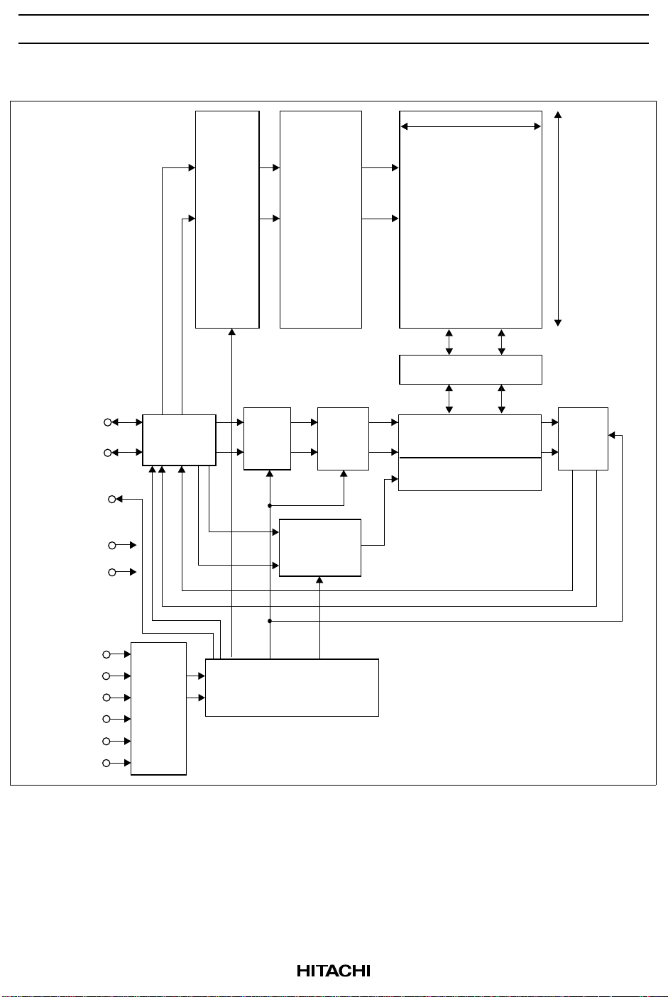
Block Diagram
2048 + 64
I/O0
to
I/O7
RDY/Busy
V
CC
V
SS
Sector
address
buffer
• •
•
Multiplexer
•
• • • • •
•
•
•
•
Data
input
buffer
X-decoder
Input
•
data
•
control
Y-address
counter
16384 × (2048 + 64) × 8
memory matrix
Data register (2048 + 64)
•
•
Y-gating
Y-decoder
16057 - 16384
Data
output
buffer
CE
OE
WE
SC
RES
CDE
4
Control
signal
buffer
Read/Program/Erase control

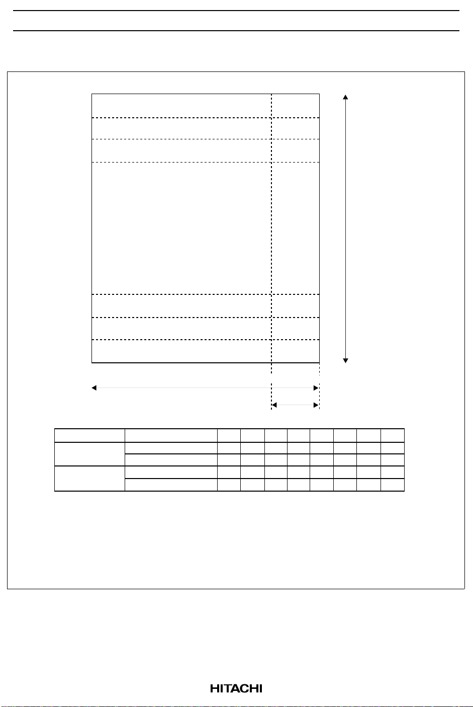
Memory Map and Address
Sector address
HN29W25611 Series
3FFFH
3FFEH
3FFDH
0002H
0001H
0000H
000H
2048 bytes
2048 bytes
2048 bytes
2048 bytes
2048 bytes
2048 bytes
64 bytes
64 bytes
64 bytes
64 bytes
64 bytes
64 bytes
800H 83FH
1
16057 - 16384 sectors *
Column address
2048 + 64 bytes
Control bytes
I/O6
I/O5
I/O4
I/O3
I/O2
I/O1
Address
Sector address
Column address
Notes: 1. Some failed sectors may exist in the device. The failed sectors can be recognized
by reading the sector valid data written in a part of the column address 800 to 83F
(The specific address is TBD.). The sector valid data must be read and kept outside
of the sector before the sector erase. When the sector is programmed, the sector
valid data should be written back to the sector.
2. An × means "Don't care". The pin level can be set to either V
to DC characteristics.
Cycles
SA (1): First cycle
SA (2): Second cycle
CA (1): First cycle
CA (2): Second cycle
I/O0
A0
A8
A0
A8
A1
A9
A1
A9
A2
A10
A2
A10
A3
A11
A3
A11
A5
A4
A13
A12
A5
A4
×
×
or VIH, referred
IL
A6
×*
A6
I/O7
A7
2
×
A7
×
×
5

HN29W25611 Series
Pin Function
CE: CE is used to select the device. The status returns to the standby at the rising edge of CE in the reading
operation. However, the status does not return to the standby at the rising edge of CE in the busy state in
programming and erase operation.
OE: Memory data and status register data can be read, when OE is VIL.
WE: Commands and address are latched at the rising edge of WE.
SC: Programming and reading data is latched at the rising edge of SC.
RES: RES pin must be kept at the V
in the memory is protected against unintentional erase and programming. RES must be kept at the V
(VSS ± 0.2 V) level when VCC is turned on and off. In this way, data
ILR
IHR
(V
CC
± 0.2 V) level during any operations such as programming, erase and read.
CDE: Commands and data are latched when CDE is VIL and address is latched when CDE is VIH.
RDY/Busy: The RDY/Busy indicates the program/erase status of the flash memory. The RDY/Busy signal
is initially at a high impedance state. It turns to a VOL level after the (40H) command in programming
operation or the (B0H) command in erase operation. After the erase or programming operation finishes, the
RDY/Busy signal turns back to the high impedance state.
I/O0 to I/O7: The I/O pins are used to input data, address and command, and are used to output memory data
and status register data.
Mode Selection
Mode CE OE WE SC RES CDE RDY/Busy*3I/O0 to I/O7
4
Deep standby ×*
Standby V
Output disable V
Status register read*
Command write*
1
2
×××V
×××V
IH
V
IL
IH
V
V
IL
IL
V
V
IL
IH
V
× V
IH
V
× V
IH
V
V
IL
IL
Notes: 1. Default mode after the power on is the status register read mode (refer to status transition). From
I/O0 to I/O7 pins output the status, when CE = V
condition).
2. Refer to the command definition. Data can be read, programmed and erased after commands are
written in this mode.
3. The RDY/Busy bus should be pulled up to V
to maintain the VOH level while the RDY/Busy pin
CC
outputs a high impedance.
4. An × means “Don’t care”. The pin level can be set to either V
× V
ILR
× V
IHR
× V
IHR
× V
IHR
V
IHRVIL
and OE = VIL (conventional read operation
IL
OH
OH
OH
OH
V
OH
or VIH referred to DC characteristics.
IL
High-Z
High-Z
High-Z
Status register outputs
Din
6

HN29W25611 Series
Command Definition*
1, 2
First bus cycle Second bus cycle
Command
Bus
cycles
Operation
3
mode*
Data in Operation
mode
Data in Data out
Read Serial read (1) (Without CA) 3 Write 00H Write SA (1)*
(With CA) 3 + 2h*6Write 00H Write SA (1)*
Serial read (2) 3 Write F0H Write SA (1)*
Read identifier codes 1 Write 90H Read ID*
Data recovery read 1 Write 01H Read Recovery
Auto erase Single sector 4 Write 20H Write SA (1)*
Auto program Program (1) (Without
CA*
7
)
4 Write 10H Write SA (1)*
(With CA*7) 4 + 2h*6Write 10H Write SA (1)*
Program (2)*
10
4 Write 1FH Write SA (1)*
Program (3) (Control bytes)*74 Write 0FH Write SA (1)*
Program (4) (WithoutCA*7) 4 Write 11H Write SA (1)*
(With CA*7) 4 + 2h*6Write 11H Write SA (1)*
Reset 1 Write FFH
Clear status register 1 Write 50H
Data recovery write 4 Write 12H Write SA (1)*
4
4
4
8, 9
data
4
4
4
4
4
4
4
4
7

HN29W25611 Series
Third bus cycle Fourth bus cycle
Bus
Command
cycles
Read Serial read (1) (Without CA) 3 Write SA (2)*
(With CA) 3 + 2h*6Write SA (2)*
Serial read (2) 3 Write SA (2)*
Read identifier codes 1
Data recovery read 1
Auto erase Single sector 4 Write SA (2)*
Auto program Program (1) (Without
CA*
7
)
4 Write SA (2)*
(With CA*7) 4 + 2h*6Write SA (2)*
Program (2)*
10
4 Write SA (2)*
Program (3) (Control bytes)*74 Write SA (2)*
Program (4) (WithoutCA*7) 4 Write SA (2)*
(With CA*7) 4 + 2h*6Write SA (2)*
Reset 1
Clear status register 1
Data recovery write 4 Write SA (2)*
Operation
mode
Data in Operation
mode
4
4
Write CA (1)*
4
4
Write B0H*
4
Write 40H
4
Write CA (1)
4
Write 40H
4
Write 40H
4
Write 40H
4
Write CA (1)
4
Write 40H
Data in
5
11
*11, 12
*11, 12
*11, 12
*11, 12
*11, 12
8

HN29W25611 Series
Fifth bus cycle Sixth bus cycle
Bus
Command
cycles
Read Serial read (1) (Without CA) 3
(With CA) 3 + 2h*6Write CA (2)*
Serial read (2) 3
Read identifier codes 1
Data recovery read 1
Auto erase Single sector 4
Auto program Program (1) (Without
CA*
7
)
4
(With CA*7) 4 + 2h*6Write CA (2)*
Program (2)*
10
4
Program (3) (Control bytes)*74
Program (4) (WithoutCA*7)4
(With CA*7) 4 + 2h*6Write CA (2) Write 40H
Reset 1
Clear status register 1
Data recovery write 4
Notes: 1. Commands and sector address are latched at rising edge of WE pulses. Program data is latched
at rising edge of SC pulses.
2. The chip is in the read status register mode when RES is set to V
3. Refer to the command read and write mode in mode selection.
4. SA (1) = Sector address (A0 to A7), SA (2) = Sector address (A8 to A13).
5. CA (1) = Column address (A0 to A7), CA (2) = Column address (A8 to A11).
(0 ≤ A11 to A0 ≤ 83FH)
6. The variable h is the input number of times of set of CA (1) and CA (2) (1 ≤ h ≤ 2048 + 64).
Set of CA (1) and CA (2) can be input not only one time but free times.
7. By using program (1) and (3), data can additionally be programmed for each sector before erase.
8. ID = Identifier code; Manufacturer code (07H), Device code (99H).
9. The manufacturer identifier code is output when CDE is low and the device identifier code is output
when CDE is high.
10.Before program (2) operations, data in the programmed sector must be erased.
11.No commands can be written during auto program and erase (when the RDY/Busy pin outputs a
V
).
OL
12.The fourth or sixth cycle of the auto program comes after the program data input is complete.
Operation
mode
Data in Operation
mode
5
5
Write 40H
first time after the power up.
IHR
Data in
*11, 12
*11, 12
9

HN29W25611 Series
Mode Description
Read
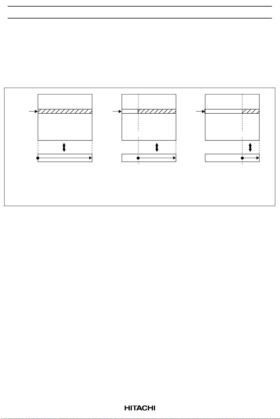
Serial Read (1): Memory data D0 to D2111 in the sector of address SA is sequentially read. Output data is
not valid after the number of the SC pulse exceeds 2112. When CA is input, memory data D (m) to D (m + j)
in the sector of address SA is sequentially read. Then output data is not valid after the number of the SC pulse
exceeds (2112 to m). The mode turns back to the standby mode at any time when CE is VIH.
Serial Read (2): Memory data D2048 to D2111 in the sector of address SA is sequentially read. Output data
is not valid after the number of the SC pulse exceeds 64. The mode turns back to the standby mode at any
time when CE is VIH.
Automatic Erase
Single Sector Erase: Memory data D0 to D2111 in the sector of address SA is erased automatically by
internal control circuits. After the sector erase starts, the erasure completion can be checked through the
RDY/Busy signal and status data polling. All the bits in the sector are "1" after the erase. The sector valid
data stored in a part of memory data D2048 to D2111 must be read and kept outside of the sector before the
sector erase.
Automatic Program
Program (1): Program data PD0 to PD2111 is programmed into the sector of address SA automatically by
internal control circuits. When CA is input, program data PD (m) to PD (m + j) is programmed from CA into
the sector of address SA automatically by internal control circuits. By using program (1), data can
additionally be programed for each sector before the following erase. When the column is programmed, the
data of the column must be [FF]. After the programming starts, the program completion can be checked
through the RDY/Busy signal and status data polling. Programmed bits in the sector turn from "1" to "0"
when they are programmed. The sector valid data should be included in the program data PD2048 to PD2111.
Program (2): Program data PD0 to PD2111 is programmed into the sector of address SA automatically by
internal control circuits. After the programming starts, the program completion can be checked through the
RDY/Busy signal and status data polling. Programmed bits in the sector turn from "1" to "0" when they are
programmed. The sector must be erased before programming. The sector valid data should be included in the
program data PD2048 to PD2111.
Program (3): Program data PD2048 to PD2111 is programmed into the sector of address SA automatically
by internal control circuits. By using program (3), data can additionally be programed for each sector befor
the following erase. When the column is programmed, the data of the column must be [FF]. After the
programming starts, the program completion can be checked through the RDY/Busy signal and status data
polling. Programmed bits in the sector turn from "1" to "0" when they are programmed.
10

HN29W25611 Series
Program (4): Program data PD0 to PD2111 is programmed into the sector of address SA automatically by
internal control circuits. When CA is input, program data PD (m) to PD (m + j) is programmed from CA into
the sector of address SA automatically by internal control circuits. By using program (4), data can be
rewritten for each sector before the following erase. So the column data before programming operation are
either "1" or "0". In this mode, E/W number of times must be counted whenever program (4) execute. After
the programming starts, the program completion can be checked through the RDY/Busy signal and status data
polling. The sector valid data should be included in the program data PD2048 to PD2111.
Sector
address
2111
16383
Memory array
0
0
Serial read (2)
Program (3)
2048
Register
2111
16383
Sector
address
Memory array
0
0
Register
Serial read (1) (Without CA)
Program (1) (Without CA)
Program (2)
2111
16383
Sector
address
Memory array
0
0
Column address
Register
Serial read (1) (With CA)
Program (1) (With CA)
Status Register Read
The status returns to the status register read mode from standby mode, when CE and OE is VIL. In the status
register read mode, I/O pins output the same operation status as in the status data polling defined in the
function description.
Identifier Read
The manufacturer and device identifier code can be read in the identifier read mode. The manufacturer and
device identifier code is selected with CDE VIL and VIH, respectively.
11

HN29W25611 Series
Data Recovery Read
When the programming was an error, the program data can be read by using data recovery read. When an
additional programming was an error, the data compounded of the program data and the origin data in the
sector address SA can be read. Output data are not valid after the number of SA pulse exeeds 2112. The
mode turns back to the standby mode at any time when CE is VIH. The read data are invalid when addresses
are latched at a rising edge of WE pulse after the data recovery read command is written.
Data Recovery Write
When the programming into a sector of address SA was an error, the program data can be rewritten
automatically by internal control circuit into the other selected sector of address SA’. In this case, top address
[SA13] of sector of address SA’ must be the same as SA. Since the data recovery write mode is internally
Program (4) mode, rewritten sector of address SA’ needs no sector erase before rewrite. After the data
recovery write mode starts, the program completion can be checked through the RDY/ Busy signal and the
status data polling.
12

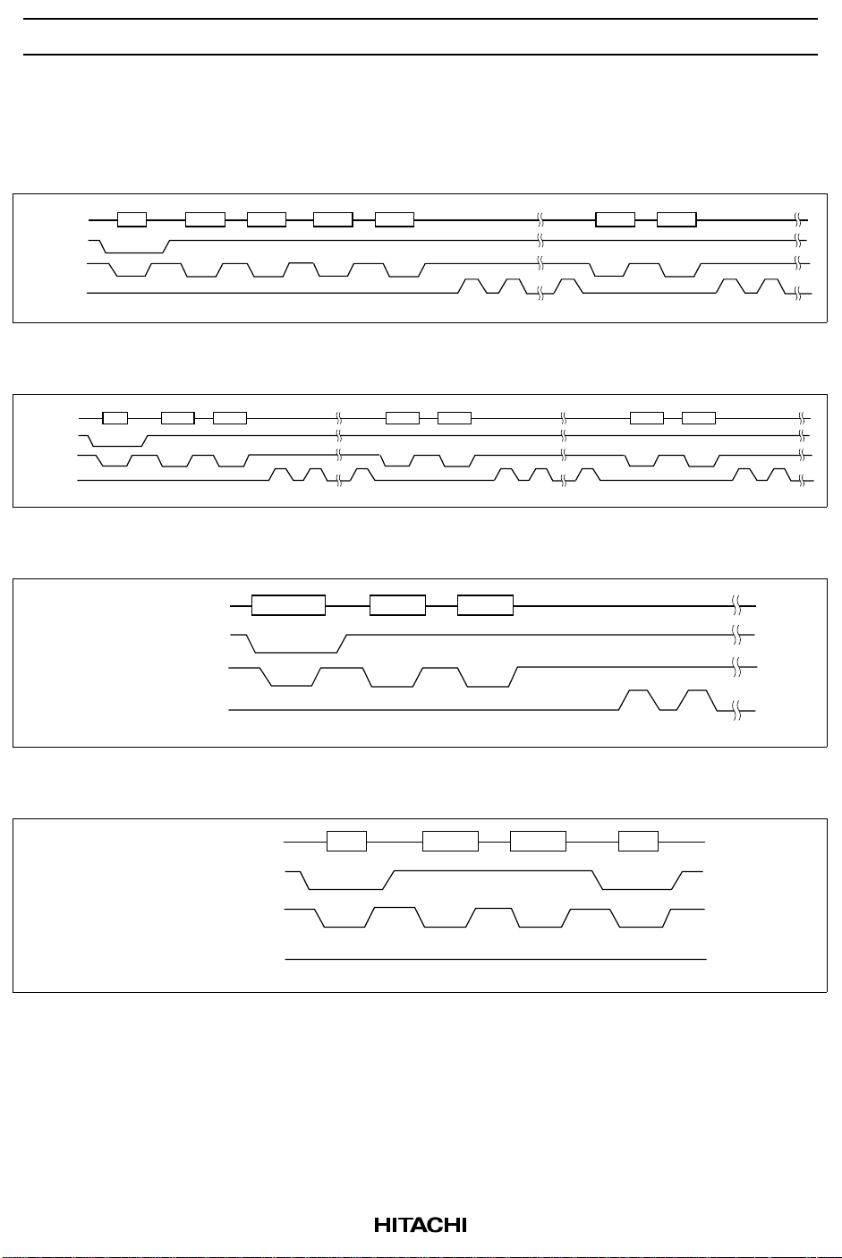
Command/Address/Data Input Sequence
Serial Read (1) (With CA before SC)
HN29W25611 Series
Command
/Address
CDE
WE
SC
00H SA (1) SA (2) CA (1) CA (2) CA (1)' CA (2)'
Low
Serial Read (1) (With CA after SC)
Command
/Address
CDE
00H SA (1) SA (2) CA (1)' CA (2)'CA (1) CA (2)
WE
Low
SC
Data output Data outputData output
Serial Read (1) (Without CA), (2)
Command/Address
CDE
WE
SC
00H/F0H SA (1) SA (2)
Low
Data output Data output
Data output
Single Sector Erase
Command/Address
CDE
WE
SC
20H B0HSA (1) SA (2)
Low
Erase start
13
 Loading...