


HA17524P/FP
Switching Regulator Controller
Features
• Pulse width modulation (PWM)
• Wide oscillation frequency range: 450 kHz(typ)
• Low quiescent current: 5 mA typ
• Good line regulation (0.2% typ) and load regulation (0.4% typ)
• Independent output stages for 2 channels
• Wide external circuit applications including single-end and push-pull method
• Reference power source output stage and switching output stage include current limiting protection
circuit.
Ordering Information
Type No. Package
HA17524P 16 pin dual in line plastic(DP-16)
HA17524FP 16 pin flat plastic (FP-16DA)
Pin Arrangement
INV.
Input
NON-INV.
Input
OSC Out
CL(+)
CL(–)
R
C
GND
T
T
1
2
3
4
5
6
7
8
(T op Vie w)
16
15
14
13
12
11
10
V
REF
V
CC
E
2
C
2
C
1
E
1
SHUT
DOWN
9
COMP
HA17524P/FP
Functional Description
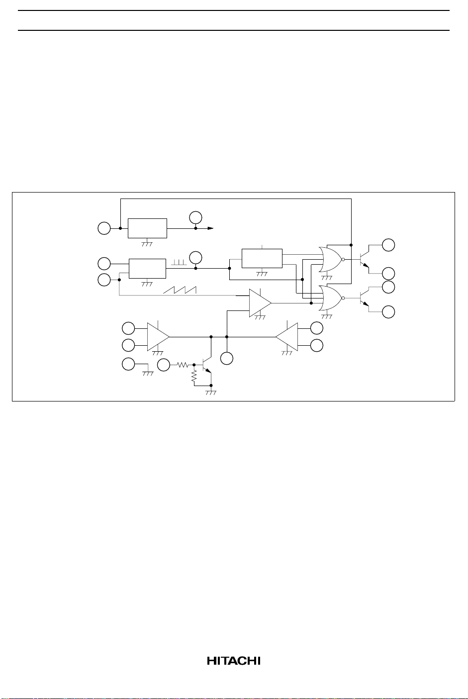
Principals of HA17524 Operation
The HA17524 switching regulator circuit, using pulse width modulation (PWM), is constructed as shown
in figure 1.
Timing resistances RT and timing capacitance CT control the oscillation frequency. CT is charged by a
constant current generated by RT. Ramp signals (saw-tooth waves) at the CT terminal generated by this
oscillator is available for reference input signal to comparator which control the pulse width.
V
REF
16
3
Comparator
Error Amp.
1kΩ
10kΩ
+5 V to internal circuitry
OSC Out
+5V
Flip Flop
+5V
—
+
COMP
9
Q
Q
+5V
+
C.L.
4
—
5
Current Limiter
NOR
NOR
CL(+)
CL(—)
12
C
1
Q
1
11
E
1
13
C
Q
2
2
14
E
2
15
V
CC
R
6
T
C
T
(Ramp)
7
INV. Input
NON-INV. Input
GND
Ref.
Volt.
+5 V
Osc.
+5V
—
1
+
2
8
10
SHUT
DOWN
Figure 1 HA17524 Block Diagram
The reference voltage connects to the non-inverted or inverted input terminal of the error amplifier via
resistance divider (figure 2).
The output voltage from the error amplifier is compared with the ramp signal capacitance CT (figure 1).
The comparator can provide a signal with modulated pulse width.
This signal, then, controls output transistors Q1 and Q2, making an open loop to stabilize output voltage.
Outputs form the error amplifier the current limiter, and the shut-down circuit are connected together at the
comparator, so that an input signal from any one of these circuits can break the output stage.
2

HA17524P/FP
V
REF
5kΩ
To Positive Regulated
Output V oltage V
R
2
O
+
5kΩ
−
R
Error Amp Error Amp
1
(a) Forward Output Stabilizing Source
R + R
V = 2.5 (V)
O
12
R
1
Figure 2 Error Amplifier Biasing
V
REF
R
5kΩ
1
+
−
R
5kΩ
2
To Negative Regulated
Output V oltage V
O
(b) Reverse Output Stabilizing Source
R + R
V = 5 − 2.5 (V)
O
21
R
1
3
HA17524P/FP
Blocks Description
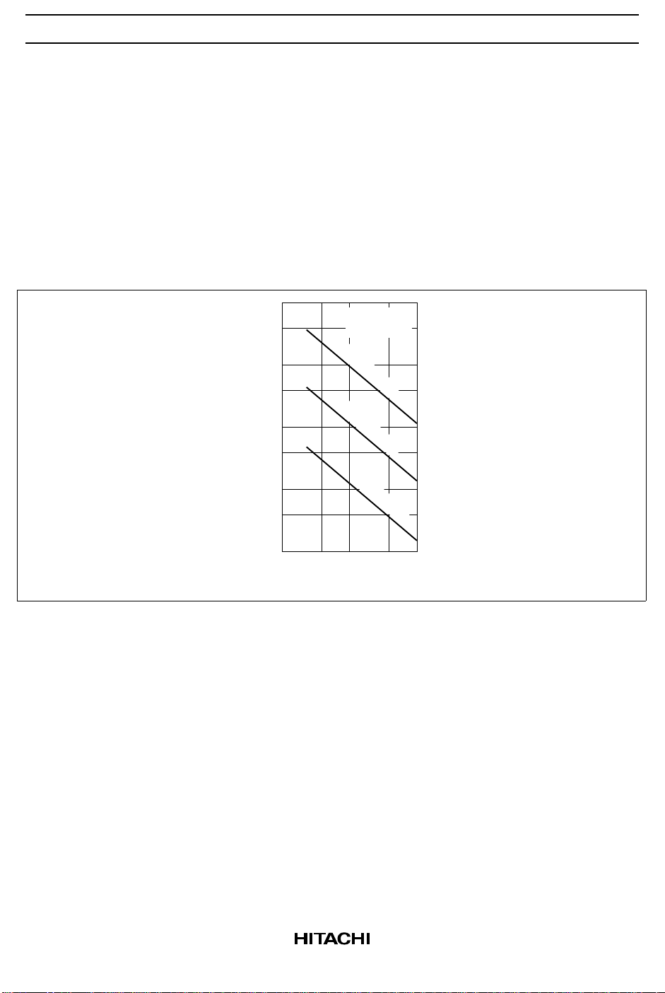
Oscillator: The oscillation frequency f is calculated from the following equations. Figure 3 shows one
example.
f 1.15/(RT•CT)
RT = 1.8k to 100 k Ω
CT = 0.001µ to 0.1 µF
f = 140 Hz to 500 kHz
1 M
400 k
100 k
40 k
10 k
4 k
1 k
Oscillating Frequency f (Hz)
400
100
1 k 4 k 10 k 40 k 100 k
Timing Resistance R ( )TΩ
V = 20 V
CC
Ta = 25°C
C = 0.001 F
T
µ
C = 0.01 F
T
µ
C = 0.1 F
T
µ
Figure 3 Oscillating Frequency vs Timing Resistance
Then the ramp wave shown in figure 4 is available at pin 7, CT terminal, since CT is charged by the constant
current I generated by RT.
4
HA17524P/FP
V
H
∆V
V
L
)
EB (Q3
R
T
3.8 – 0.9 = 2.9 V
≅
L
1
I
Q
1
6 7
II
R
T
Q
2
Q
3
Discharge
C
V
T
REF
T
C
Terminal Waveform
T
REF
H
· ∆V ·
≈
T
– VEB (Q2) – V
V
I
≈
∆V = V – V
T C
Figure 4 Oscillating Circuit and CT Terminal Waveform
The oscillator output pulse signal is used as the flip flop clock pulse and as switching pulses for the output
transistors, synchronous to the clock pulse.
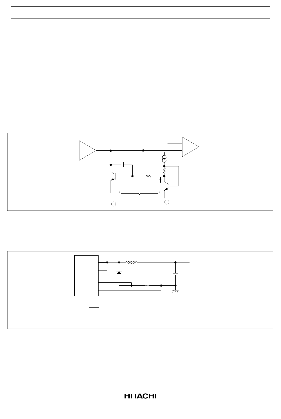
The pulse-widths which can be controlled by the timing capacitor CT as shown in figure 5, increases output
dead time.
10
V = 20 V
CC
R = 10 k
T
3
Ta = 25°C
Ω
1.0
Dead Time (µs)
0.3
0.1
0.001 0.003 0.01 0.03 0.1
Timing Capacitance C
(µF)
T
Figure 5 Dead Time vs Timing Capacitance
Reference Voltage: The built-in regulator (reference voltage: V
= 5 ±0.4 V) can be used as a reference
REF
power supply for the error amplifier, which determines output voltage (V
source for another circuits in IC.
). It is also connected as a bias
OUT
5
HA17524P/FP
Error Amplifier: Figure 2 shows error amplifier biasing, applied input voltage must be set within the range
of common-mode input voltage (1.8 V to 3.4 V). Inserting a resistor and capacitor between phase
compensation terminal (pin 9) and GND in series provides phase compensation.
Current Limiter: The sense amplifier threshold voltage (VS) for the current limiter is:
VS= VBE (Q ) + I1R2 – V
= I1R
2
BE (Q2
)
= 200 mV typ
At the current limiter sense amp shown in figure 6, when V+ – V– 200 mV, Q1 turns on, phase
compensation terminal becomes low and the output switching element is cut off.
Error
Amp
Q
1
(–)C.L.
V –
Comp
Sense Amp
C
T
Comparator
R
R
2
1
Q
2
I
1
(+)C.L.
V +
Figure 6 Current Limiter Sense Amplifier
Figure 7 shows an example of detecting current limit. The input voltage range is –0.7 V to +1.0 V; The
current limit detection output is provided from GND line.
E
1
E
2
+V
OUT
HA17524
CL(–)
CL(+)
V
S
=
I
OS
R
S
R
S
VS = 200 mV
Figure 7 Current Limit Detector Example Operating Waveforms
6
 Loading...