

HIT 2SB561 Datasheet
Application
• Low frequency power amplifier
• Complementary pair with 2SD467
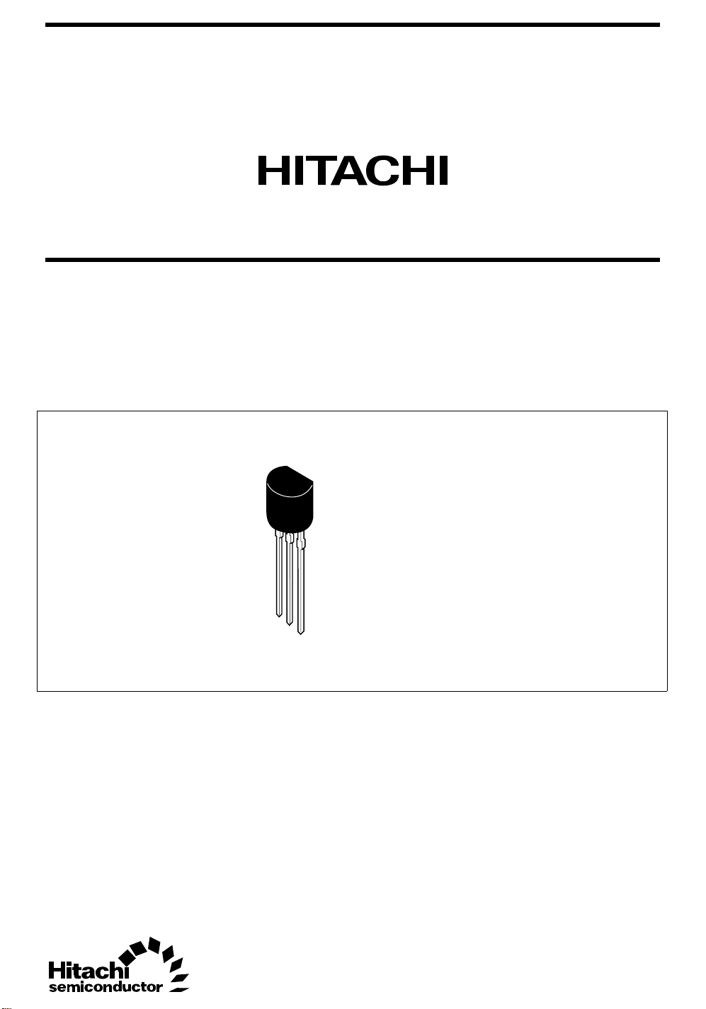
Outline
TO-92 (1)
2SB561
Silicon PNP Epitaxial
1. Emitter
2. Collector
3. Base
3
2
1
2SB561
Absolute Maximum Ratings (Ta = 25°C)
Item Symbol Ratings Unit
Collector to base voltage V
Collector to emitter voltage V
Emitter to base voltage V
Collector current I
Collector peak current i
Collector power dissipation P
CBO
CEO
EBO
C
C(peak)
C
Junction temperature Tj 150 °C
Storage temperature Tstg –55 to +150 °C
Electrical Characteristics (Ta = 25°C)
Item Symbol Min Typ Max Unit Test conditions
Collector to base breakdown
V
(BR)CBO
voltage
Collector to emitter breakdown
V
(BR)CEO
voltage
Emitter to base breakdown
V
(BR)EBO
voltage
Collector cutoff current I
CBO
DC current transfer ratio hFE*
Collector to emitter saturation
V
CE(sat)
voltage
Base to emitter voltage V
Gain bandwidth product f
BE
T
Collector output capacitance Cob — 20 — pF VCB = –10 V, IE = 0
Note: 1. The 2SB561 is grouped by hFE as follows.
BC
85 to 170 120 to 240
–25 — — V IC = –10 µA, IE = 0
–20 — — V IC = –1 mA, RBE = ∞
–5——V I
— — –1.0 µAVCB = –20 V, IE = 0
1
85 — 240 VCE = –1 V,
— –0.2 –0.5 V IC = –0.5 A, IB = –0.05 A
— –0.75 –1.0 V VCE = –1 V, IC = –0.15 A
— 350 — MHz VCE = –1 V, IC = –0.15 A
–25 V
–20 V
–5 V
–0.7 A
–1.0 A
0.5 W
= –10 µA, IC = 0
E
I
= –0.15 A (Pulse test)
C
f = 1 MHz
2
 Loading...