

HIT 2SB1048 Datasheet
Application
High gain amplifier
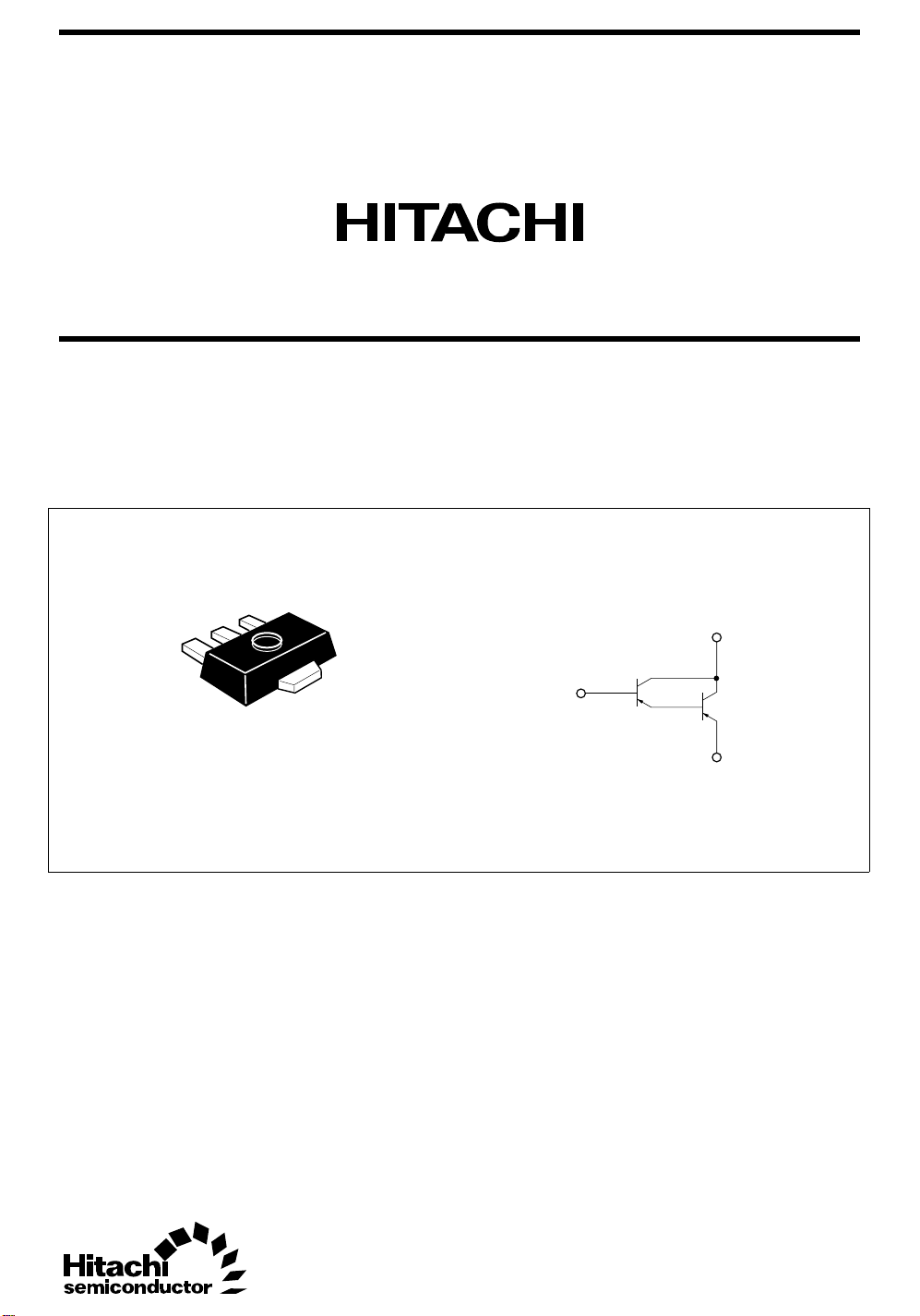
Outline
UPAK
3
2SB1048
Silicon PNP Epitaxial, Darlington
1
2
2,4
4
1. Base
2. Collector
3. Emitter
4. Collector (Flange)
1
3
2SB1048
Absolute Maximum Ratings (Ta = 25°C)
Item Symbol Ratings Unit
Collector to base voltage V
Collector to emitter voltage V
Emitter to base voltage V
Collector current I
Collector peak current i
Collector power dissipation PC*
CBO
CEO
EBO
C
C(peak)
1
*
2
Junction temperature Tj 150 °C
Storage temperature Tstg –55 to +150 °C
Notes: 1. PW ≤ 10 ms, Duty cycle ≤ 20%
2. Value on the alumina ceramic board (12.5 × 30 × 0.7 mm)
Electrical Characteristics (Ta = 25°C)
Item Symbol Min Typ Max Unit Test conditions
Collector to base breakdown
voltage
Collector to emitter breakdown
voltage
Collector cutoff current I
Emitter cutoff current I
DC current transfer ratio h
Collector to emitter saturation
voltage
Base to emitter saturation
voltage
Notes: 1. Pulse test
2. Marking is “BT”
V
(BR)CBO
V
(BR)CEO
CBO
EBO
FE
V
CE(sat)
V
BE(sat)
–60 — — V IC = –10 µA, IE = 0
–60 — — V IC = –1 mA, RBE = ∞
— — –10 µAVCB = –60 V, IE = 0
— — –10 µAVEB = –7 V, IE = 0
2000 — 100000 VCE = –3 V, IC = –500 mA*
— — –2.0 V IC = –500 mA, IB = –1 mA*
— — –2.0 V IC = –500 mA, IB = –1 mA*
–60 V
–60 V
–7 V
–1 A
–2 A
1W
1
1
1
2
 Loading...