HIT 2SA778A, 2SA778 Datasheet

2SA778(K), 2SA778A(K)
Application
High voltage medium speed switching
Outline
TO-92 (1)
Silicon PNP Epitaxial
1. Emitter
2. Collector
3. Base
3
2
1

2SA778(K), 2SA778A(K)
Absolute Maximum Ratings (Ta = 25°C)
Item Symbol 2SA778(K) 2SA778A(K) Unit
Collector to base voltage V
Collector to emitter voltage V
Emitter to base voltage V
Collector current I
Collector power dissipation P
CBO
CEO
EBO
C
C
Junction temperature Tj 150 150 °C
Storage temperature Tstg –55 to +150 –55 to +150 °C
Electrical Characteristics (Ta = 25°C)
2SA778(K) 2SA778A(K)
Item Symbol Min Typ Max Min Typ Max Unit Test conditions
Collector to base
breakdown voltage
Collector to emitter
breakdown voltage
Collector cutoff current I
Emitter cutoff current I
DC current transfer ratio h
Collector to emitter
saturation voltage
Base to emitter
saturation voltage
Collector output
capacitance
Gain bandwidth product f
Turn on time t
Turn off time t
Storage time t
V
(BR)CBO
V
(BR)CER
CBO
–150 — — –180 — — V IC = –50 µA, IE = 0
–150 — — –180 — — V IC = –50 µA,
— — –1.0 — — — µAVCB = –100 V, IE = 0
— — — — — –1.0 µAVCB = –150 V, IE = 0
— — –1.0 — — –1.0 µAVEB = –5 V, IC = 0
30 100 — 40 100 200 VCE = –3 V,
— –0.3 –1.0 — –0.3 –1.0 V IC = –15 mA,
— –0.77 –1.0 — –0.77 –1.0 V IC = –15 mA,
V
V
EBO
FE
CE(sat)
BE(sat)
Cob — — 10 — — 10 pF VCB = –10 V, IE = 0,
T
on
off
stg
— 50 — — 50 — MHz VCE = –3 V,
— 135 — — 135 — ns VCC = –10.3 V
— 1.7 — — 1.7 — µsIC = 10 IB1 = –10
— — 1.0 — — 1.0 µsVCC = –10 V,
–150 –180 V
–150 –180 V
–5 –5 V
–50 –50 mA
200 200 mW
R
= 30 kΩ
BE
I
= –15 mA
E
I
= –1 mA
B
I
= –1 mA
B
f = 1 MHz
I
= –15 mA
C
I
= –10 mA
B2
I
=–17 mA
C
I
= –1mA,
B1
I
= –12 mA
B2
2

2SA778(K), 2SA778A(K)
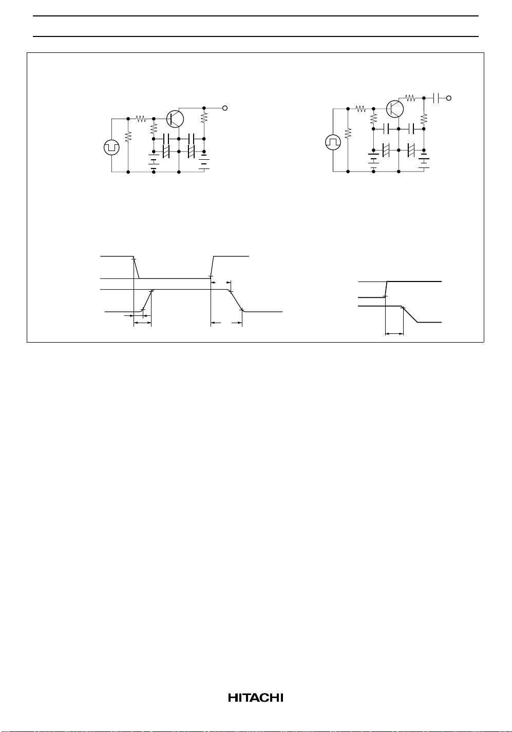
t
on
P.G.
tr, t
15ns
≤
f
PW 5µs
≤
duty ratio 10%
≤
Input
–13 V
Output
Switching Time Test Circuit
, t
Test Circuit
off
6 k
D.U.T.
6 k
0.002 0.002
+–+–
6 V –10.3 V
505050
Response Waveform
0
0
10%
10%
t
d
90%
t
on
CRT
1 k
UnitR : Ω
C : µF
90%
t
stg
t
off
`
10%
90%
P.G.
≤
, t
5ns
t
r
f
≥
PW 5µs
duty ratio = 50%
Switching Time Test Circuit
Test Circuit
t
stg
0.1
2.4 k
D.U.T
0.002 0.002
50
–++–
Response Waveform
+7 V
Input
0
10%
0
Output
t
stg
510
5050
10%
0.1
CRT
16
–10 V–3 V
UnitR : Ω
C : µF
3
 Loading...