


HIT 2SA715 Datasheet
2SA715
Silicon PNP Epitaxial
Application
Low frequency power amplifier complementary pair with 2SC1162
Outline
TO-126 MOD
1. Emitter
2. Collector
1
2
3
3. Base
Absolute Maximum Ratings (Ta = 25°C)
Item Symbol Rating Unit
Collector to base voltage V
Collector to emitter voltage V
Emitter to base voltage V
Collector current I
Collector peak current I
Collector power dissipation P
Junction temperature Tj 150 °C
Storage temperature Tstg –55 to +150 °C
Note: 1. Value at TC = 25°C
CBO
CEO
EBO
C
C(peak)
C
PC*
1
–35 V
–35 V
–5 V
–2.5 A
–3 A
0.75 W
10 W
2SA715
Electrical Characteristics (Ta = 25°C)
Item Symbol Min Typ Max Unit Test conditions
Collector to base breakdown
V
(BR)CBO
voltage
Collector to emitter breakdown
V
(BR)CEO
voltage
Emitter to base breakdown
V
(BR)EBO
voltage
Collector cutoff current I
CBO
DC current transfer ratio hFE*
h
FE
Base to emitter voltage V
Collector to emitter saturation
V
BE
CE(sat)
voltage
Gain bandwidth product f
T
Note: 1. The 2SA715 is grouped by hFE as follows.
–35 — — V IC = –1 mA, IE = 0
–35 — — V IC = –10 mA, RBE = ∞
–5 — — V IE = –1 mA, IC = 0
— — –20 µAVCB = –35 V, IE = 0
1
60 — 320 VCE = –2 V, IC = –0.5 A
20 — — VCE = –2 V, IC = –1.5 A
(Pulse test)
— –1.0 –1.5 V VCE = –2 V, IC = –1.5 A
(Pulse test)
— –0.5 –1.0 V IC = –2 A, IB = –0.2 A
(Pulse test)
— 160 — MHz VCE = –2 V, IC = –0.2 A
(Pulse test)
BCD
60 to 120 100 to 200 160 to 320
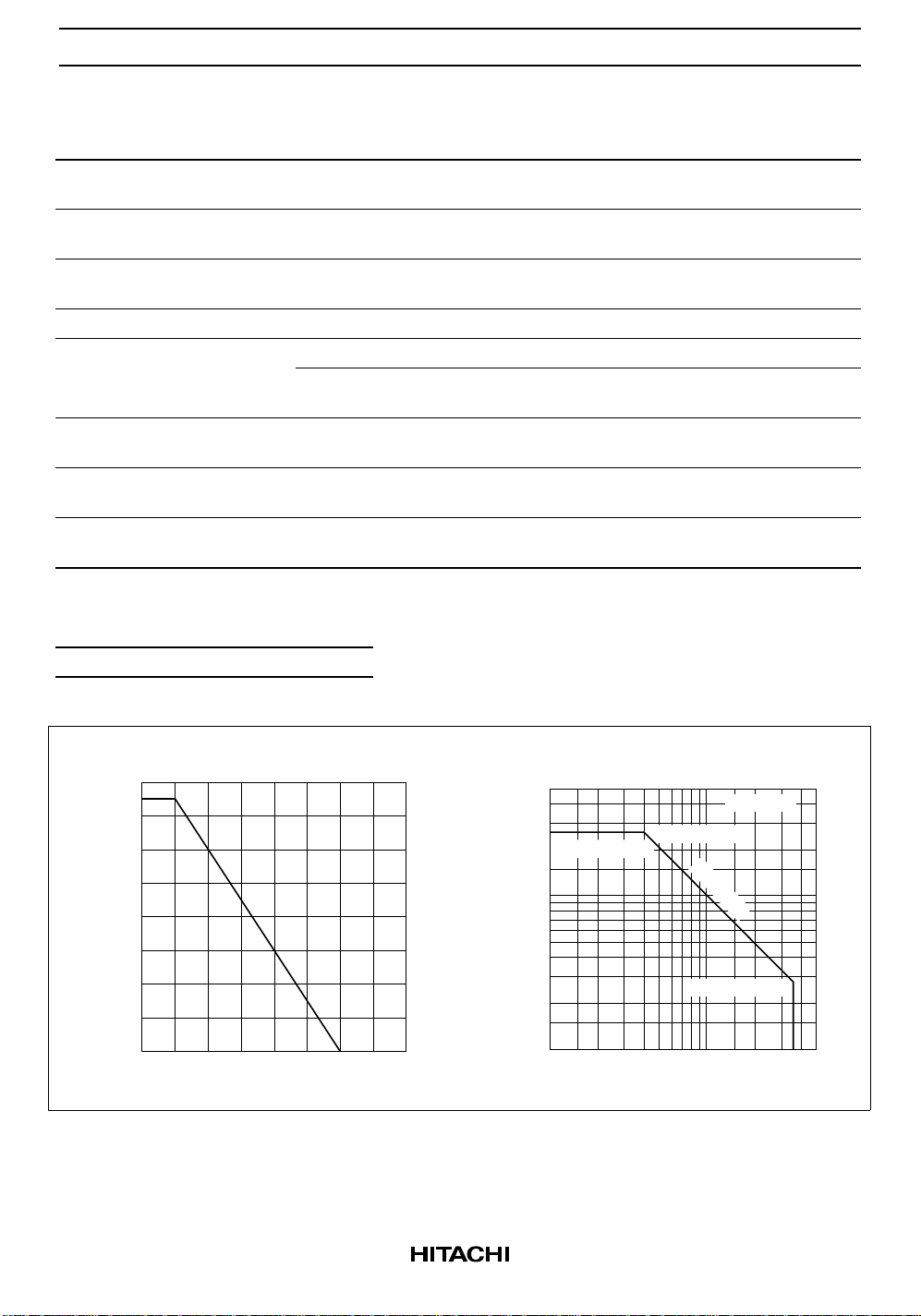
Maximum Collector Dissipation
Curve
0.8
0.6
0.4
0.2
Collector power dissipation Pc (W)
0 50 100 150 200
Ambient temperature Ta (°C)
–5
IC max(DC Operation)
–2
(A)
C
–1.0
–0.5
Collector current I
–0.2
–0.1
–1 –2 –5 –10
Area of Safe Operation
TC = 25°C
(–4 V,–2.5 A)
P
C
= 10 W
(–35 V,–0.28 A)
–20 –50
Collector to emitter voltage V
CE
(V)
2