

HIT 2SA1171 Datasheet
Application
Low frequency small signal amplifier
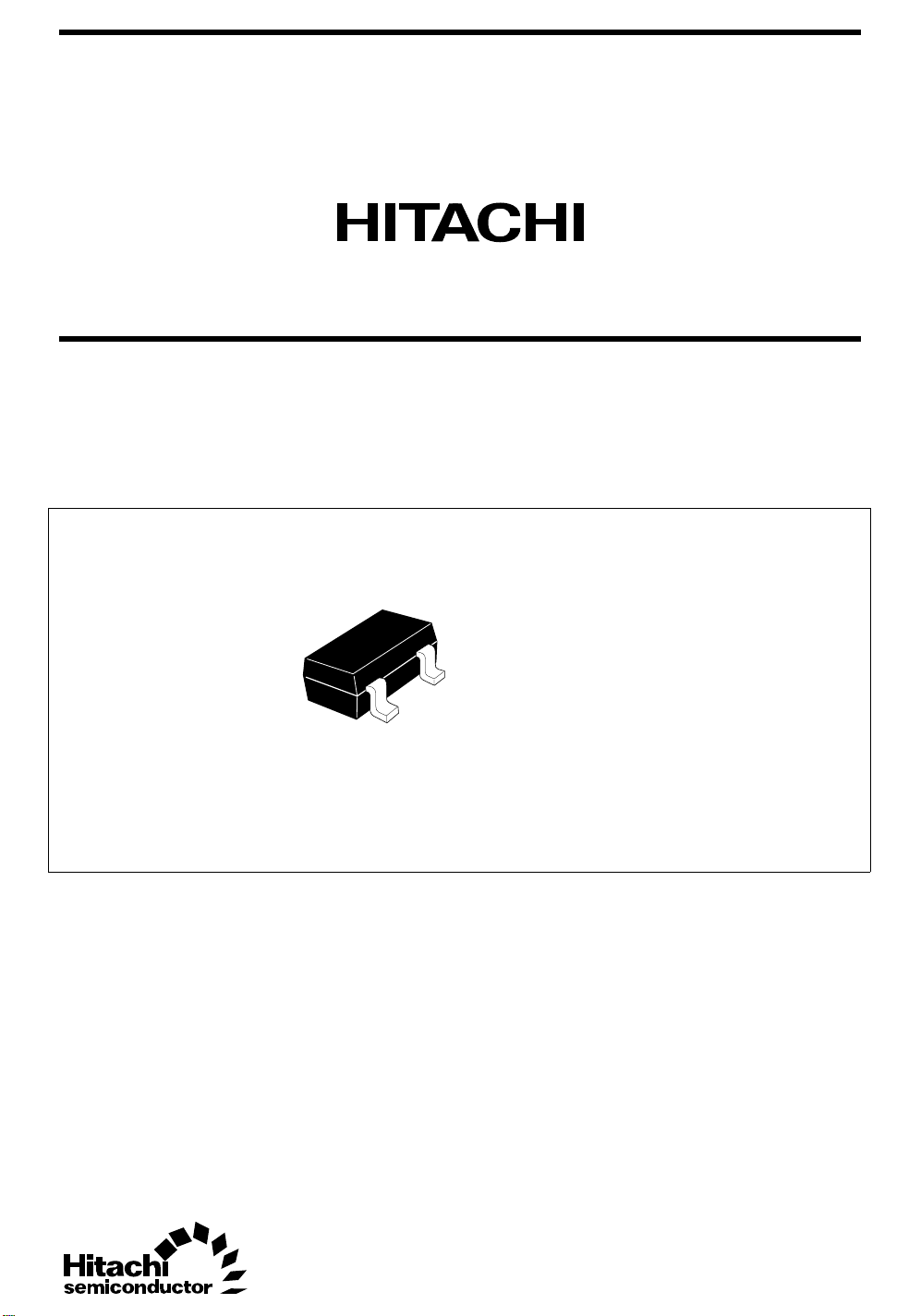
Outline
MPAK
2SA1171
Silicon PNP Epitaxial
3
1
2
1. Emitter
2. Base
3. Collector

2SA1171
Absolute Maximum Ratings (Ta = 25°C)
Item Symbol Ratings Unit
Collector to base voltage V
Collector to emitter voltage V
Emitter to base voltage V
Collector current I
Collector power dissipation P
CBO
CEO
EBO
C
C
Junction temperature Tj 150 °C
Storage temperature Tstg –55 to +150 °C
Electrical Characteristics (Ta = 25°C)
Item Symbol Min Typ Max Unit Test conditions
Collector to emitter breakdown
V
(BR)CEO
voltage
Collector cutoff current I
CBO
DC current transfer ratio hFE*
Base to emitter voltage V
Collector to emitter saturation
V
BE
CE(sat)
voltage
Gain bandwidth product f
T
Collector output capacitance Cob — 1.6 — pF VCB = –25 V, IE = 0, f = 1 MHz
Note: 1. The 2SA1171 is grouped by hFE as follows.
Grade D E
Mark PD PE
h
FE
250 to 500 400 to 800
–90 — — V IC = –1 mA, RBE = ∞
— — –0.5 µAV
1
250 — 800 V
— — –0.75 V VCE = –12 V, IC = –2 mA
— — –0.5 V IC = –10 mA, IB = –1 mA
— 200 — MHz VCE = –12 V, IC = –2 mA
–90 V
–90 V
–5 V
–50 mA
150 mW
= –75 V, IE = 0
CB
= –12 V, IC = –2 mA
CE
See characteristic curves of 2SA872.
2
 Loading...