

Page 1
AUDIOACCESS
MA-361/MA-361CP
TWELVE CHANNEL DIGITAL AMPLIFIER
PRELIMINARY SERVICE MANUA L
Harman Consumer Group
250 Crossways Park Dr.
Woodbury, New York 11797
Page 2

MA
-
361
Audioaccess®Twelve Channel Digital
Amplifier
www.audioaccess.com
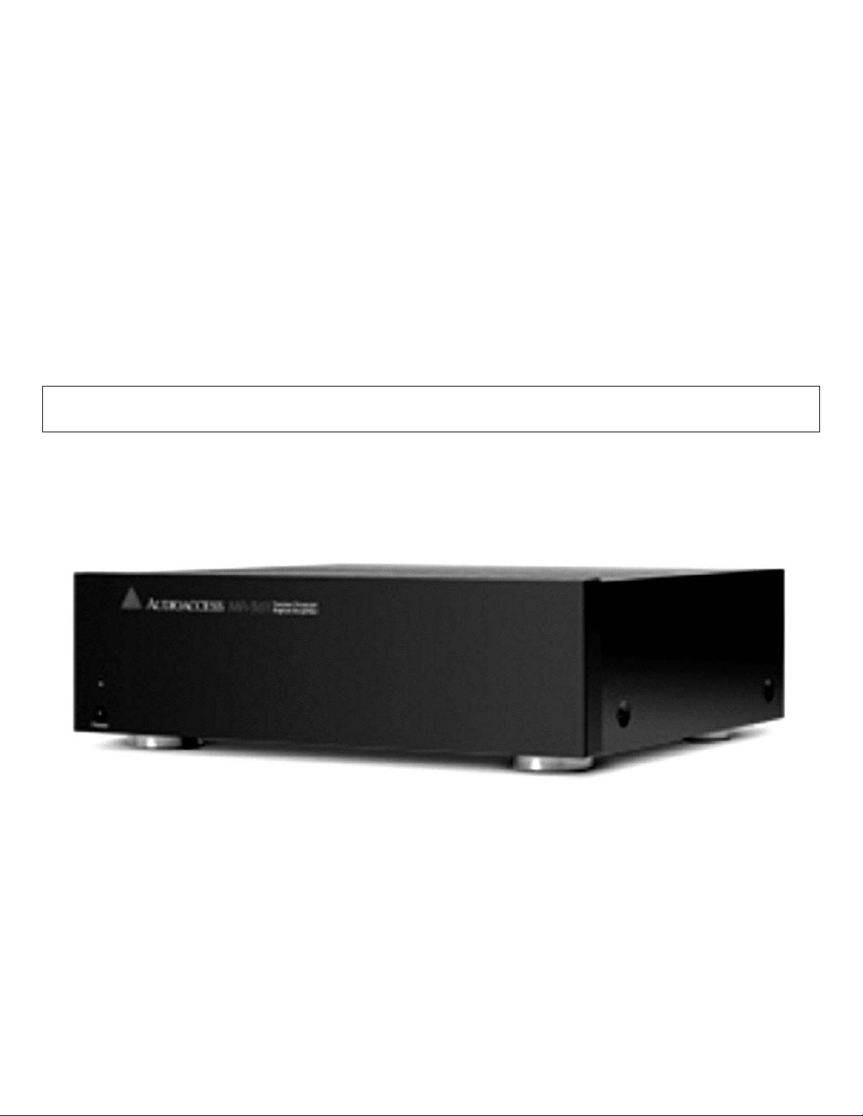
The Audioaccess MA-361 Twelve Channel
Digital Amplifier—designed, engineered
and manufactured by Madrigal in
Middletown, CT—will no doubt be recognized as the finest amplifier available for
use in any dedicated multi-room system
application. The product of over two years
of development and research, the goals of
the MA-361 were clear: high power, low
distortion, quiet, cool operation, outstanding sonics and ease of installation not only
with associated Audioaccess components,
but also with other home and commercial
audio distribution systems. The trend
towards use of higher quality and larger
speaker systems for custom installed applications has created a need for power
amplification offering both true higher
power levels with low distortion. The
MA-361 is a category leading product that
finally addresses the evolution of high
quality custom audio systems.
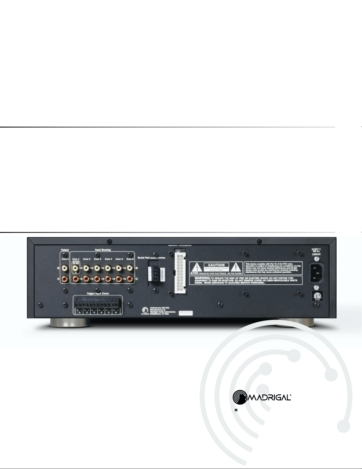
Main Features
Some of the main features of the MA-361
include a conservative power rating of
100 Watts per channel into 8 Ohms from
20Hz-20kHz with all channels driven,
7-band graphic equalization programmable on a per-zone basis, signal sensing,
and voltage triggers to activate main
power in each stereo zone of amplification. In normal use, the MA-361 runs
amazingly cool, thanks to its highly efficient
digital design. A modular layout permits
the installing dealer to easily replace individual amplifier modules, should service
ever be required. The MA-361 can be
configured for use in either mono or
stereo operation by means of dip-switches on the rear panel of the amplifier. A
simple bussing scheme allows audio
signals to be routed to a single zone,
selected zones, or all areas. To aid in both
the pre-wiring phase of the project and in
final installation, a speaker termination
board—available separately—allows the
dealer to complete the speaker wiring to
the termination board during the preliminary phase of the project. Later, upon final
installation, the termination board is then
plugged directly into a slot on the back of
the amplifier, minimizing the chances of
wiring errors within the system.
7-Band Graphic Equalization
The MA-361’s 7-band graphic equalization
capabilities allows the installing dealer to
custom tailor the sound in each zone to
compensate for the different room acoustics
throughout a residence, maximizing the
performance of each pair of speakers.
Signal Sensing and Voltage Triggers
The signal sensing capabilities of the
MA-361 ensure that the amplifiers for a
given zone are only powered on when a
particular area is active, saving on energy
consumption. Voltage triggers allow the
MA-361 to automatically turn on accessory
items such as a fan, or a separate device
when either the amplifier or a designated
zone is activated.
Simply Ingenious
Page 3
A Harman International Company
Audioaccess
®
Madrigal Audio Laboratories, Inc.
P.O.Box 781
Middletown, CT 06457-0781
Internet: www.madrigal.com
Fax: 860.346.1540 ©2002 Madrigal Audio Laboratories, Inc.
20201AA – SS/MA-361
Volume/Tone Control Modules
Optional Volume/Tone Control Modules,
which plug into available slots inside the
amplifier, provide the dealer with the
ability to supply high power at very low
distortion levels to expansion rooms
within the multi-room system. A total of
6 Volume/Tone Control Modules may be
installed in the MA-361.
Flexible Installation Capabilities
The MA-361 is designed for use not only
with Audioaccess systems, but also with
other Multi-room or RS-232 based systems.
The unit is programmed with the proprietary Installation Manager application
when it is used with other Audioaccess
Multi-Room components. Configuration
settings are downloaded from a Windows
PC or laptop via the RS-485 communication port on the MA-361. When used with
other RS-232 based systems, a separate
application is available, which downloads
amplifier configuration settings via the
RS-232 port on the MA-361CP version.
Summary
The combination of the MA-361’s power
capabilities, sonic quality, features, programming ease, installation flexibility and
serviceability clearly sets the new standard
for amplifiers within the multi-room category.
Features
Specifications
Number of Channels:
▲ 12, configured as 6 left/right mono or
stereo pairs (zones)
Power Output:
▲ 100 Watts @ 8 Ω, from 20Hz – 20kHz,
all channels driven
130 Watts @ 4 Ω, from 20Hz – 20kHz,
all channels driven
200 Watts @ 4 Ω, from 20Hz – 20kHz,
single channels driven
Efficiency:
▲ 93% @ 100 Watts/8Ω
THD & Noise:
▲ < 0.3%, 0.1 Watt – 200 Watts, 4Ω
IMD:
▲ 0.26% @ 4Ω, 200 Watts
Frequency response:
▲ ± 0.3 dB at rated power, 8Ω load
Bandwidth:
▲ 60kHz at rated power, 8Ω load
Signal/Noise:
▲ 97dB unweighted (ref: rated power) into 8 Ω
Crosstalk:
▲ -84 dB between any two channels
(no audible crosstalk)
Protection:
▲ Short Circuit, Over Current, DC, Thermal
and Undervoltage
Muting:
▲ Turn-on, Turn-off, Signal Sensing and
Triggered per zone
Input Impedance:
▲ 20K Ω
Input Sensitivity:
▲ 1.3 Volt for full output 4 or 8Ω
Gain:
▲ 27dB
Dimensions:
▲ 171⁄4"W x 51⁄8"H x 175⁄8"D
(438 mm x 130 mm x 448 mm)
(with connectors & feet)
Weight:
▲ 110 Volt Amplifier: 48 lb (21.8 kg)
230 Volt Amplifier: 51 lb (23.2 kg)
Features, specifications and dimensions are subject to change.
▲ 6 built-in 7-Band Graphic EQ, one per zone
▲ Signal sensing
▲ Voltage trigger for each zone set with remov-
able screw terminal
▲ Available in two versions: MA-361 with RS-485
port and MA-361CP with RS-232 port
▲ Optional modules configured by Audioaccess
Installation Manager application or stand-alone
PC program
▲ Dual-color LED status indicator on front panel
illuminates Green for normal operation, Red for
standby and a flashing Red for DC and/or thermal protection
▲ AC mains switch on front panel
Easy installation
▲ Simple built-in input bussing scheme, no con-
figuration switches required
▲ Plug-in TI-501 Speaker Termination Board, a
snap for advance installations (available separately, not included with amplifier)
Modular construction
▲ Amplifier modules may be replaced quickly
and easily
▲ Permits installation of optional modules
Upgradeable
▲ Firmware upgradeable
▲ Optional EM-401 Volume/Tone Control mod-
ule for all six zones (available separately)
▲ Download project settings via serial port using
Installation Manager application or dedicated
stand-alone software
Robust design
▲ Low voltage standby (brown out protection)
▲ Short circuit protection
▲ Thermal cutoff protection
▲ Soft clipping
▲ Quiet, convection cooling (when properly
installed according to factory recommendations)
▲ UL/CSA/CE approved
Page 4

FEATURES
The Audioacc ess MA-361 T welve Channel Digital Amplifi er – designed, engineered and manufactur ed by Madrigal in
Middletown, CT – r epr esents the pr oduc t of over two years of research and developm ent.
As the inventor of the 12 channel amplifier category, Audioaccess has reinvented this cat egor y with the introduction of the
MA-361. The goals for the MA - 361 were clear: high power, low distortion, quiet, cool operation, outstanding sonics and
ease of install ation, when used not only in Audioaccess system s, but also with other home and comm ercial audio
distributi on systems. The trend towards higher qual ity and larger speakers for c ustom installed applications has created a
need for this amp. W e believ e y ou will agr ee that the MA-361 is the first in an entirely new class of twelve channel
amplifiers.
Unique features
The main featur es of the MA - 361 incl ude a c onservative power rating of 100 Wat ts per channel into 8 Ohms from 20Hz20kHz with all channels driven at 93% efficiency. Thi s amazing eff ic iency not only minimizes power consum ption, it also
runs surprisingly cool. Other unique features i nc lude programmable 7-band graphic EQ (set by the installer vi a PC) f or
each zone and optional plug-in stereo Volume/T one Control Modules, which pro-vide volume control in Expansion
rooms/sub zones within an Audioaccess system or another RS - 232 based cont r ol system. The modular lay out permi ts the
dealer to easily r eplac e individual amplifi er modules should service ever be required. An ex ternal speaker termination
board can be ordered in adv anc e t o allow termination of loudspeakers before the amplifier is delivered for final install ation.
At final, simpl y pl ug the speaker termination board onto t he r ear panel of the amplifier.
Other features
To make the amplifier specifically attractive for use in whole-house audio distribution, we have included specif ic features
to ensure reliable and easy installation. Si gnal sensing and voltage triggers activ ate the main power in each stereo zone
of amplific ation. Dip switches on the rear-panel configure the MA-361 for use in either m ono or ster eo oper ation. A simple
bussing scheme all ows audio signals to be routed into a single zone, sel ected z ones, or all areas.
7-Band Gr a phic Equa liz a tion
The MA-361’s 7-band graphi c equalization capabilities allows the installing dealer to custom tailor the sound in each zone
to compensate for the different room acoustics thr oughout a residence, maximi zi ng the performance of each pair of
speakers. Thi s i s accom plished by using the Audioaccess Installation Manager Software application (or stand-alone
applicati on) r unning on the dealer’s PC or laptop.
Signal Sensing and Voltage Triggers
The signal sensing capabilities of the MA-361 ensure that t he am plifiers for a given zone are only powered on when a
particular ar ea is active, saving on energy consumpti on. Voltage triggers all ow the MA - 361 to automatically turn on
accessory it em s such as a fan, or a separat e dev ic e when either the amplifier or a designat ed z one is activated.
Volume/Tone Cont rol Modules
Optional Volume/Tone Control Modules, which pl ug into available slots inside t he am plifier, provide the abilit y to supply
high power at very low distortion levels to expansion rooms within the multi-r oom system. The user may control the
volume in rooms with Audioaccess keypads and touchscreens, or by using ANY other touch screen/control systems. A
total of 6 Volume/Tone Control Modules may be installed in the MA - 361.
Flexible Installation Capabilities
The MA-361 is designed for use with Audioaccess systems, as well as other Multi-room or RS- 232 based systems. The
unit is programmed with the proprietary Installation Manager applic ation when it is used with other Audioac c ess MultiRoom component s. Confi gur ation settings are downloaded from a Windows PC or laptop via the RS-485 communicati on
port on the MA-361. When used with ot her RS - 232 based system s, a separat e application is available, which downloads
amplifi er confi gur ation settings via the RS-232 port on the MA-361CP v er si on.
Summary
The MA-361’s com bination of power capabiliti es, soni c quality, features, programming ease, installati on fl exi bility and
serviceability clearly sets the new standard for amplifiers within the m ulti-room category.
Page 5
Specifications:
• Number of Channels: 12, c onfigured as 6 left/right mono or stereo pai r s (zones)
• Power Output: 100 Wat ts @ 8 ohms, from 20Hz — 20kHz, all channels driven
• 130 Watts @ 4 ohms, from 20Hz — 20kHz, all channels driven
• 200 Watts @ 4 ohms, from 20Hz — 20kHz, two channels driven
• Efficiency: 93% @ 100 W att s/8 ohm s
• THD & Noise:< 0.3%, 0.1 Watt — 200 Watts, 4 ohms IMD:- 0.26% @ 4 ohms 200 Watts
• Frequency response: ± 0.3 dB at rated power, 81Ú2 load
• Bandwidth: 60kHz at r ated power, 81Ú2 load
• Signal/Noi se: 97dB unweighted (ref: rated power) i nto 8 1Ú2
• Crosstalk: - 84 dB bet ween any two channel s (no audible crosstalk)
• Protection: S hor t Circuit, Over Current, DC, Thermal and Undervoltage
• Muting: Tur n- on, T ur n- off , Signal Sensing and Triggered per zone
• Input Impedance: 20K
• Input Sensitiv ity: 1.3 Volt for full output 4 or 81Ú2
• Gain: 27dB
• Dimensions: 17 1/4"W x 5 1/8"H x 17 5/8"D (438 mm x 130 mm x 448 mm) (with connectors & feet)
• Weight:110 Volt Amplifier: 48 lb (21.8 kg), 230 Volt Amplifier: 51 lb (23.2 kg)
Features, specifications and dimensions are subj ec t to change.
Page 6

MA-361 AUDIO BOARD REMOVAL AND ASSEMBLY INSTRUCTIONS
Madrigal Audio Laboratories
P.O. Box 781
Middletown, CT 06457-0781
(860) 346-0896 FAX (860) 347-6251
# A041102
Page 7

Audioaccess
APRIL 15, 2002 A041102
AUDIO BOARD DISASSEMBLY INSTRUCTIONS
Table of Contents
Overview.................................................................................................................................................. 3
Affected Units ..........................................................................................................................................3
Cautions before Beginnning ...................................................................................................................3
Tools Required.........................................................................................................................................3
Disassembly/Reassembly Steps ..............................................................................................................4
Removal/Assembly Sheets......................................................................."A" Process Description Sheets
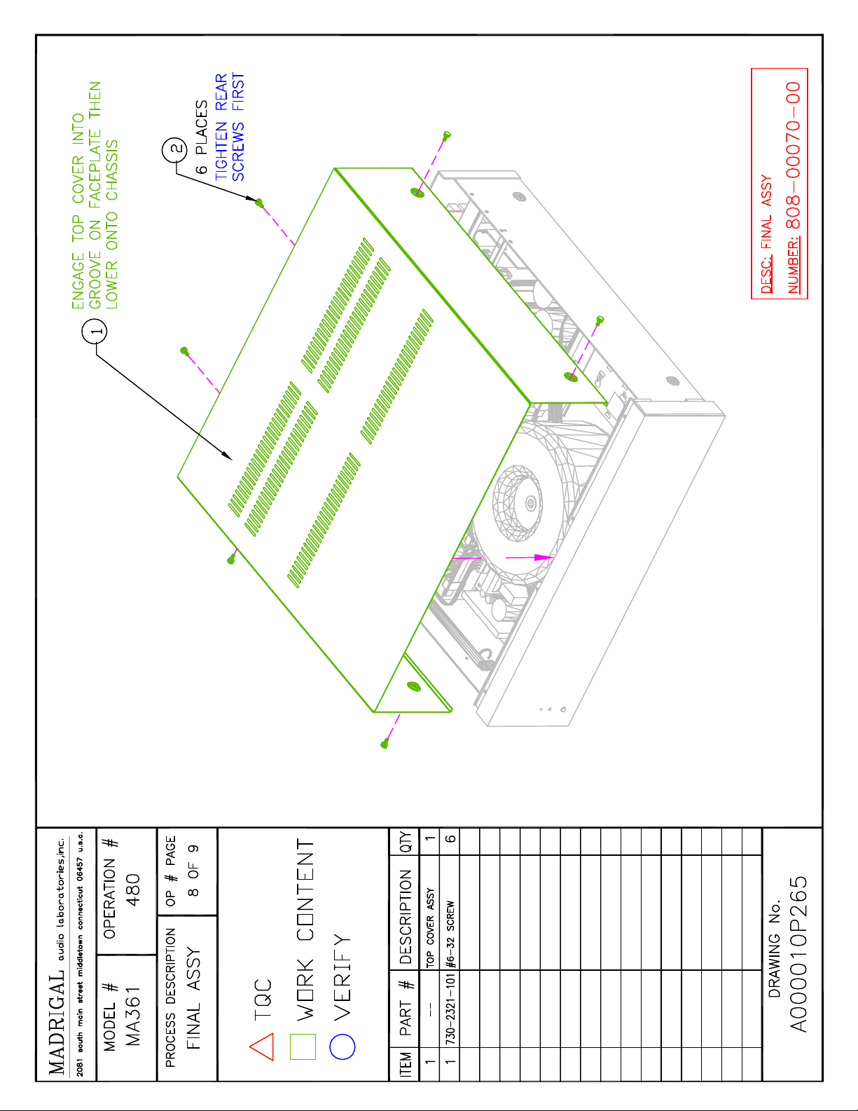
Step 1 Remove Top Cover......................................................................................................... A000010P265
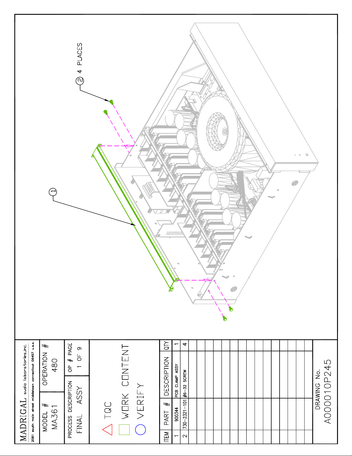
Step 2 Remove Larger PCP Clamp Assembly ............................................................................A000010P245
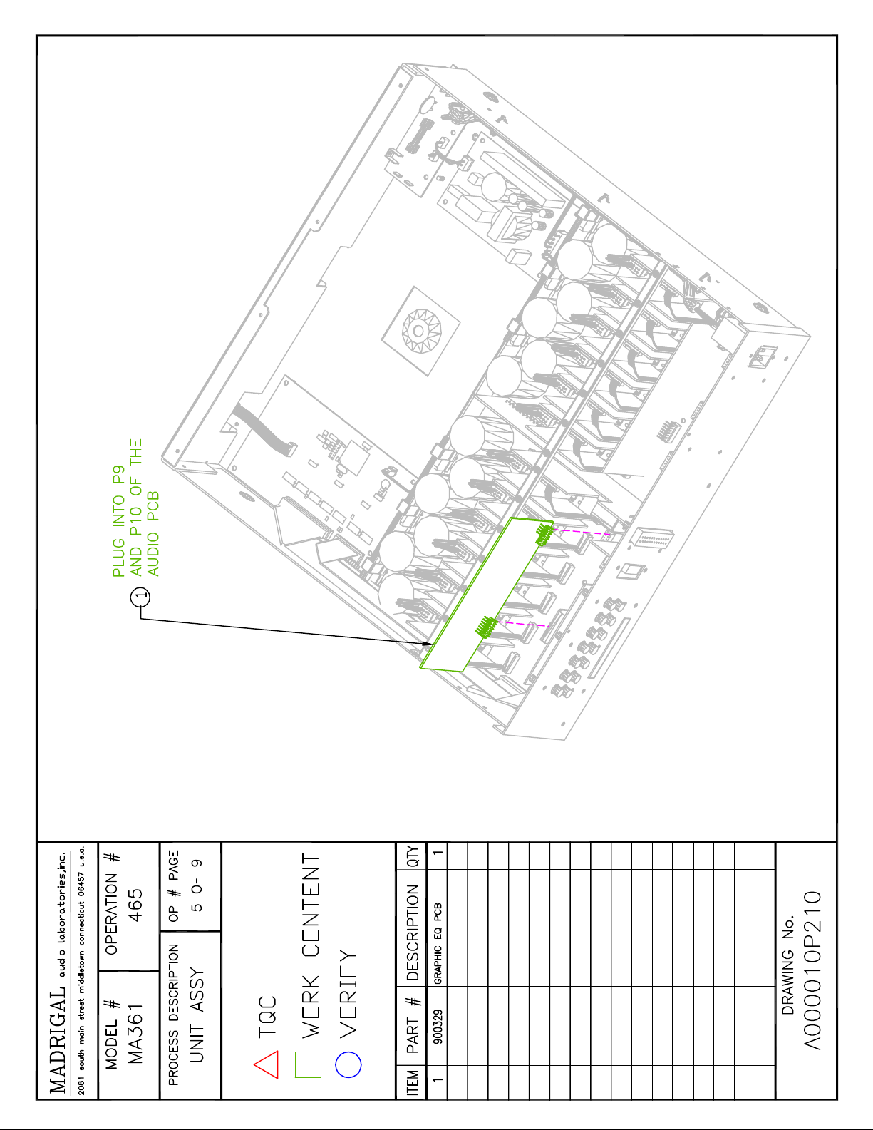
Step 3 Remove First Graphic EQ PCB ....................................................................................... A000010P210
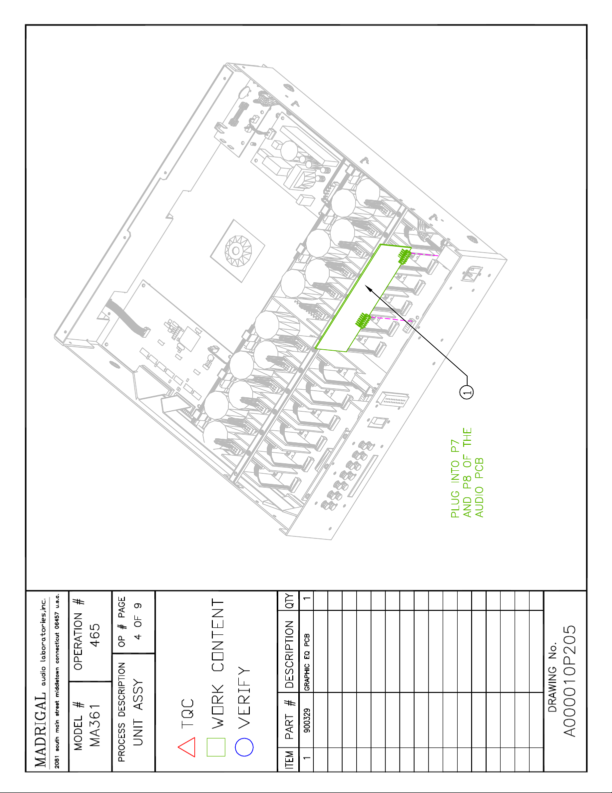
Step 4 Remove Second Graphic EQ PCB .................................................................................. A000010P205
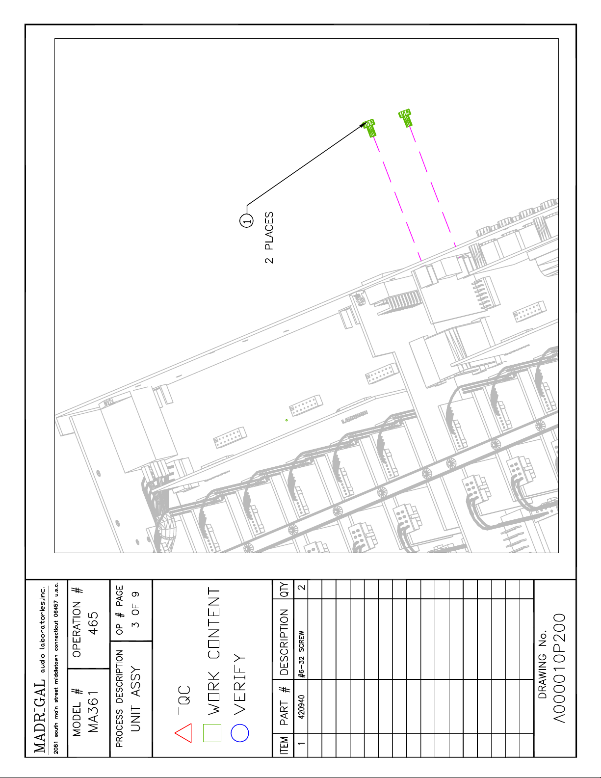
Step 5 Remove Screws Holding RS -232/485 PCB ...................................................................... A000010P200
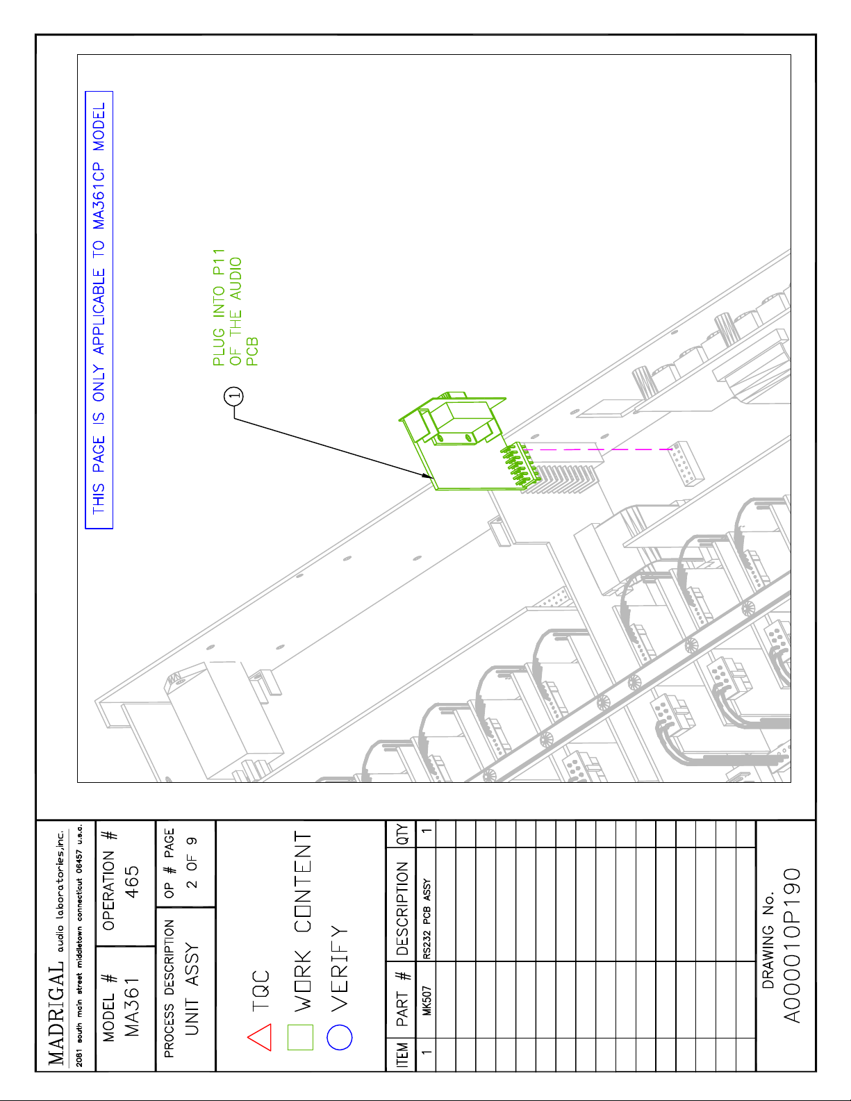
Step 6 Remove RS -232 PCB (CP Model Specific).......................................................................A000010P190
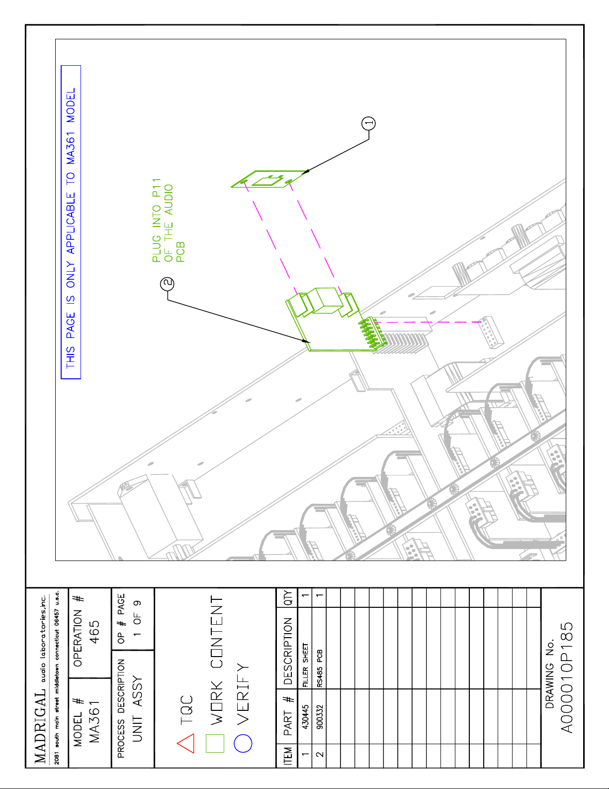
Step 7 Remove RS-485 PCB (Standard MA 361 Specific)............................................................ A000010P185
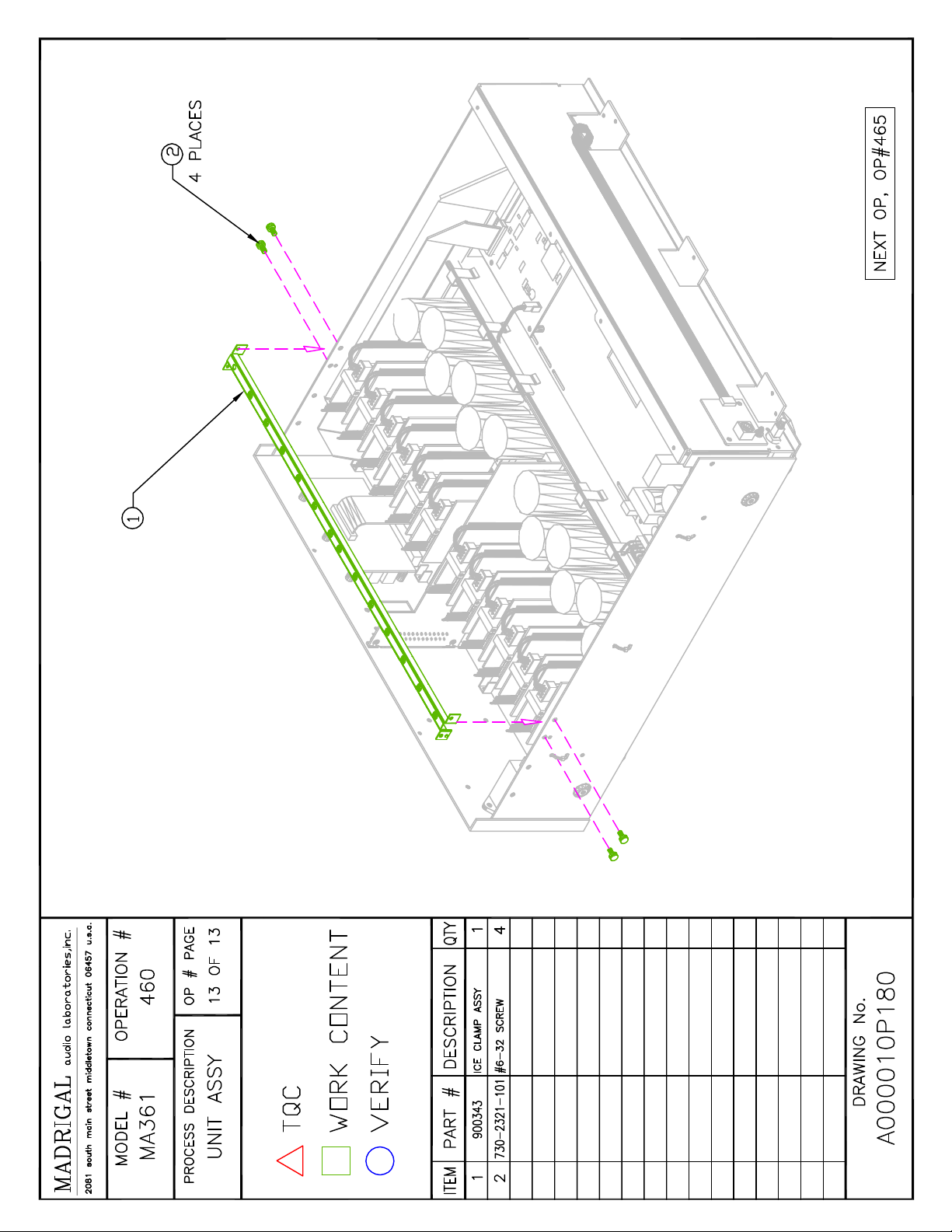
Step 8 Remove Amp Module Clamp Assembly ........................................................................... A000010P180
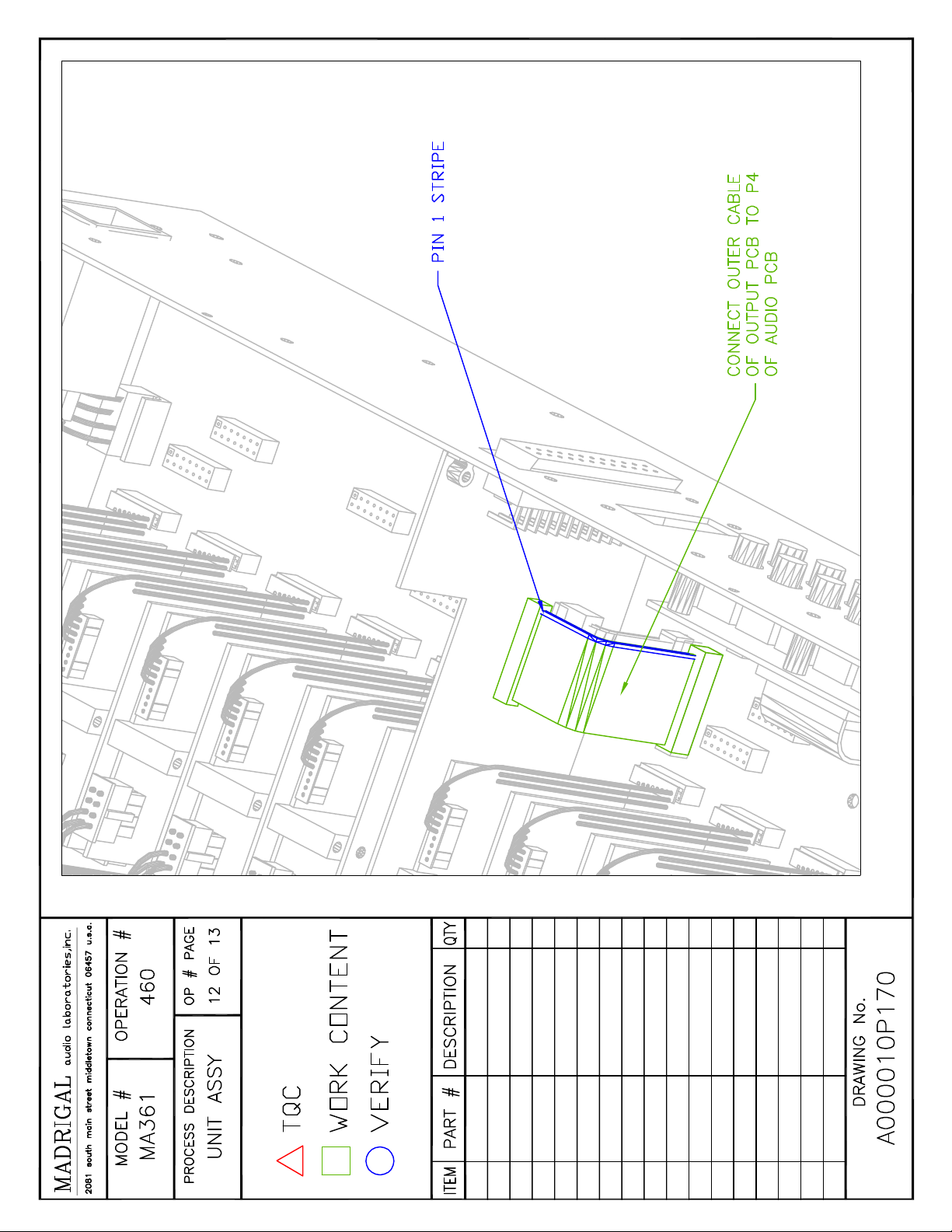
Step 9 Remove Outer Ribbon to Audio Output PCB .................................................................... A000010P170
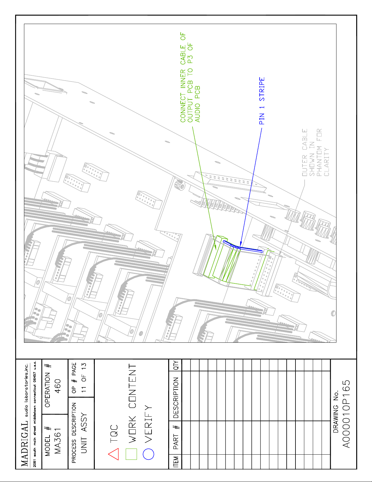
Step 10 Remove Inner Ribbon to Audio Output PCB .................................................................... A000010P165
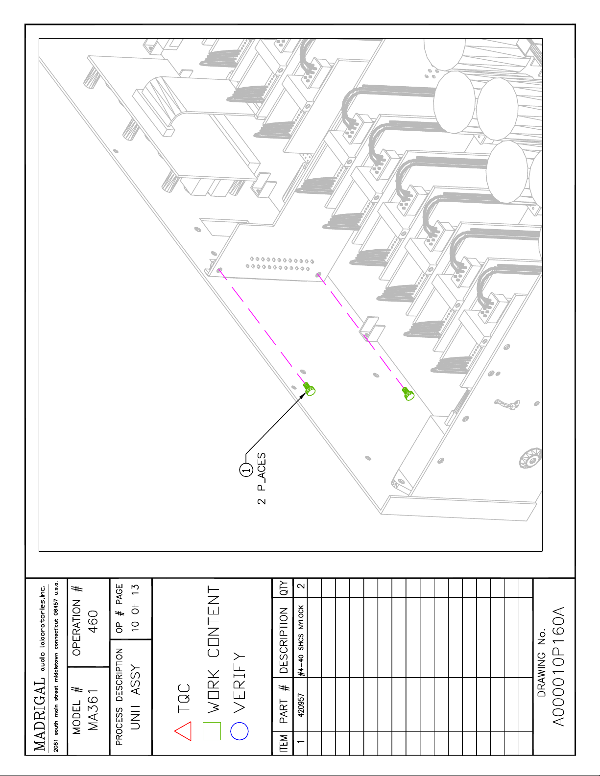
Step 11 Remove Screws on Audio Output PCB ........................................................................A000010P160A
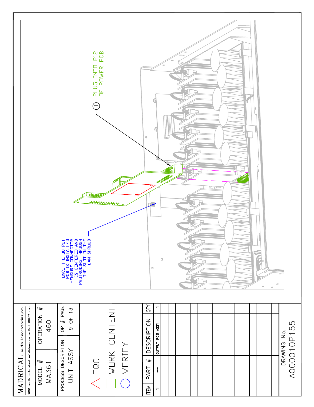
Step 12 Remove Audio Output PCB .......................................................................................... A000010P155
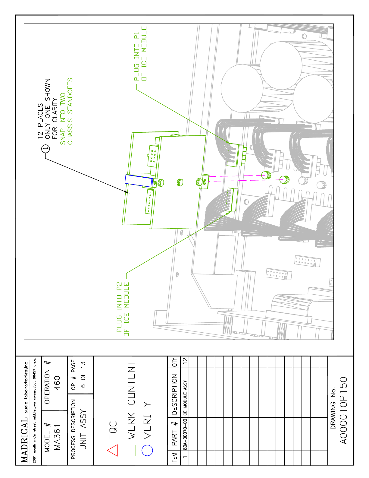
Step 13 Remove Audio Modules ................................................................................................ A000010P150
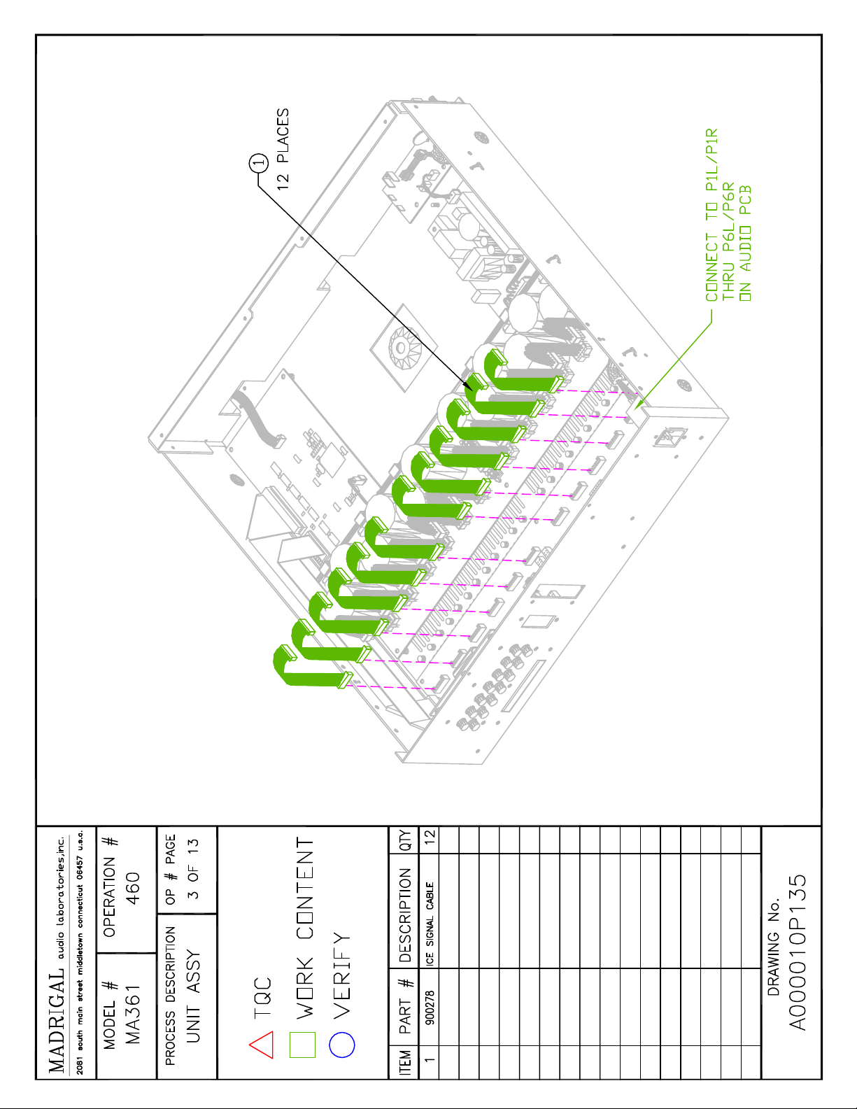
Step 14 Remove Audio Module Signal Cables ............................................................................ A000010P135
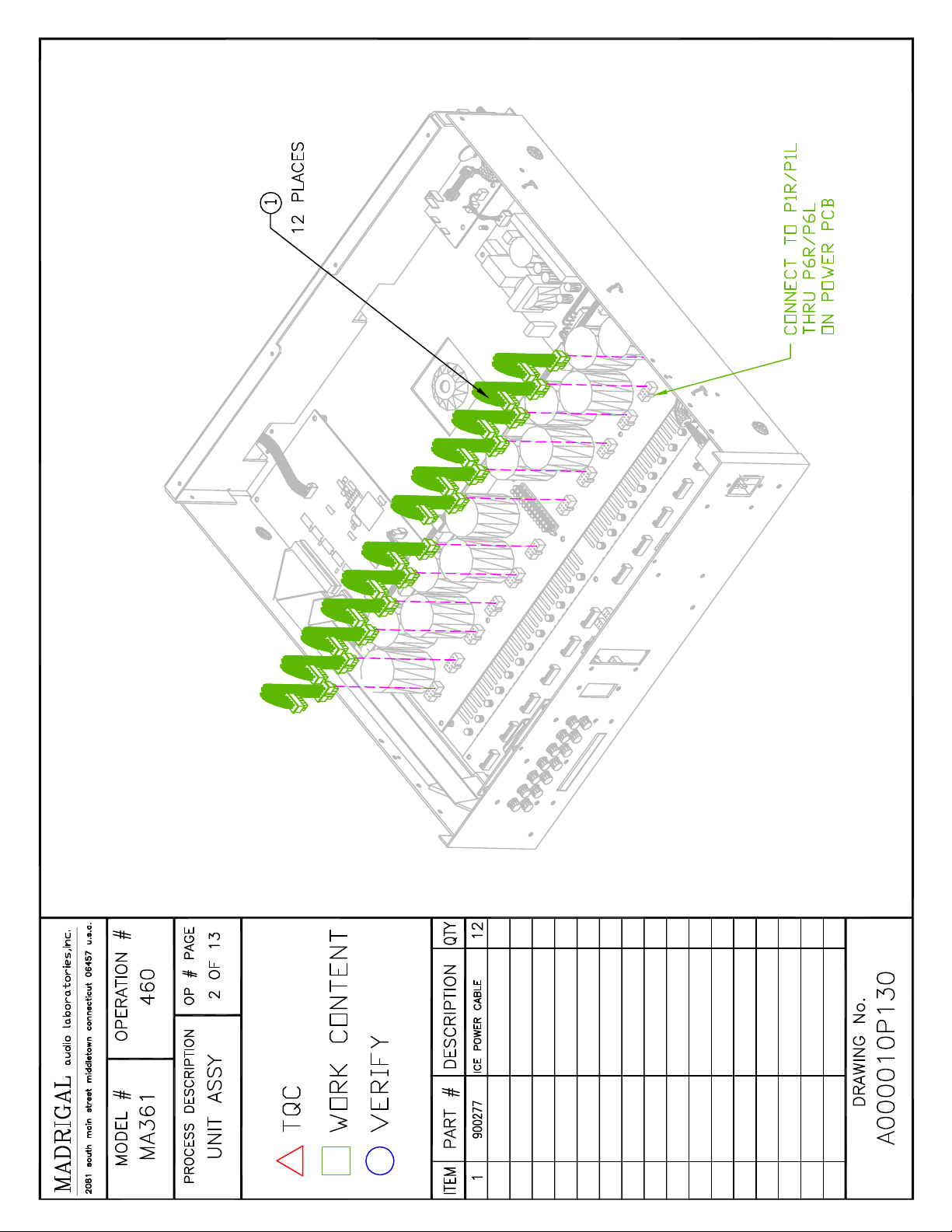
Step 15 Remove Audio Module Power Cables ............................................................................ A000010P130
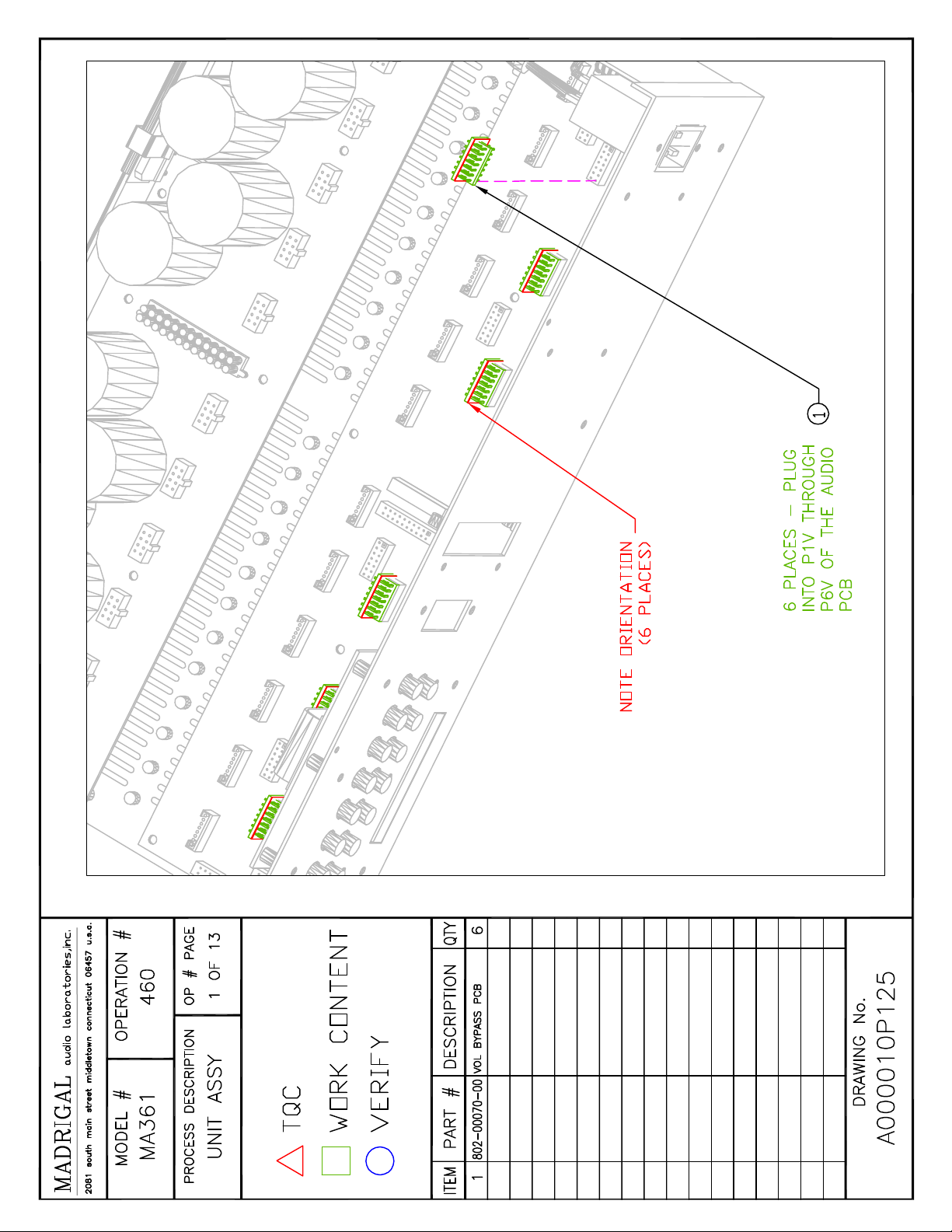
Step 16 Remove Volume Bypass Jumpers.................................................................................A000010P125
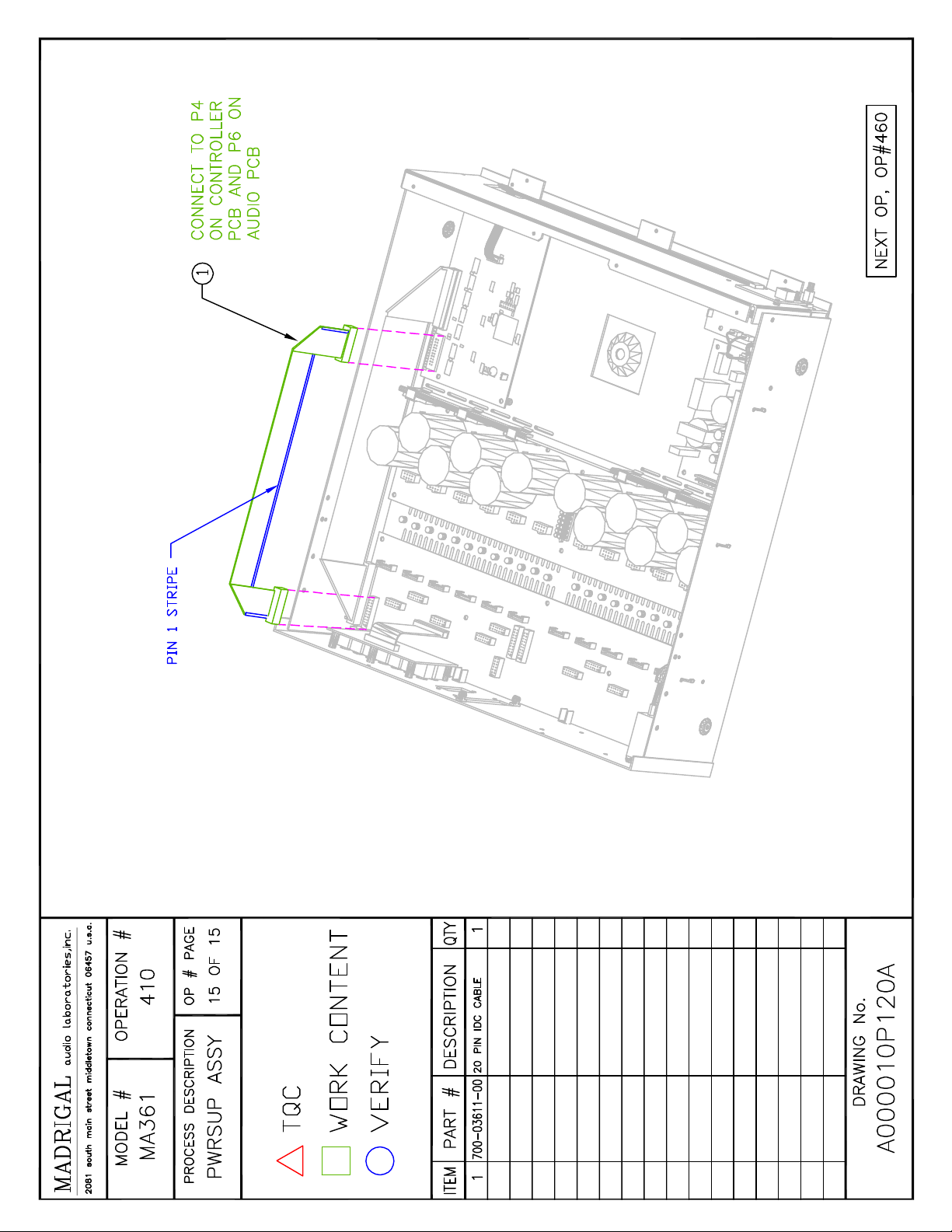
Step 17 Remove 20 Pin Ribbon Cable......................................................................................A000010P120A
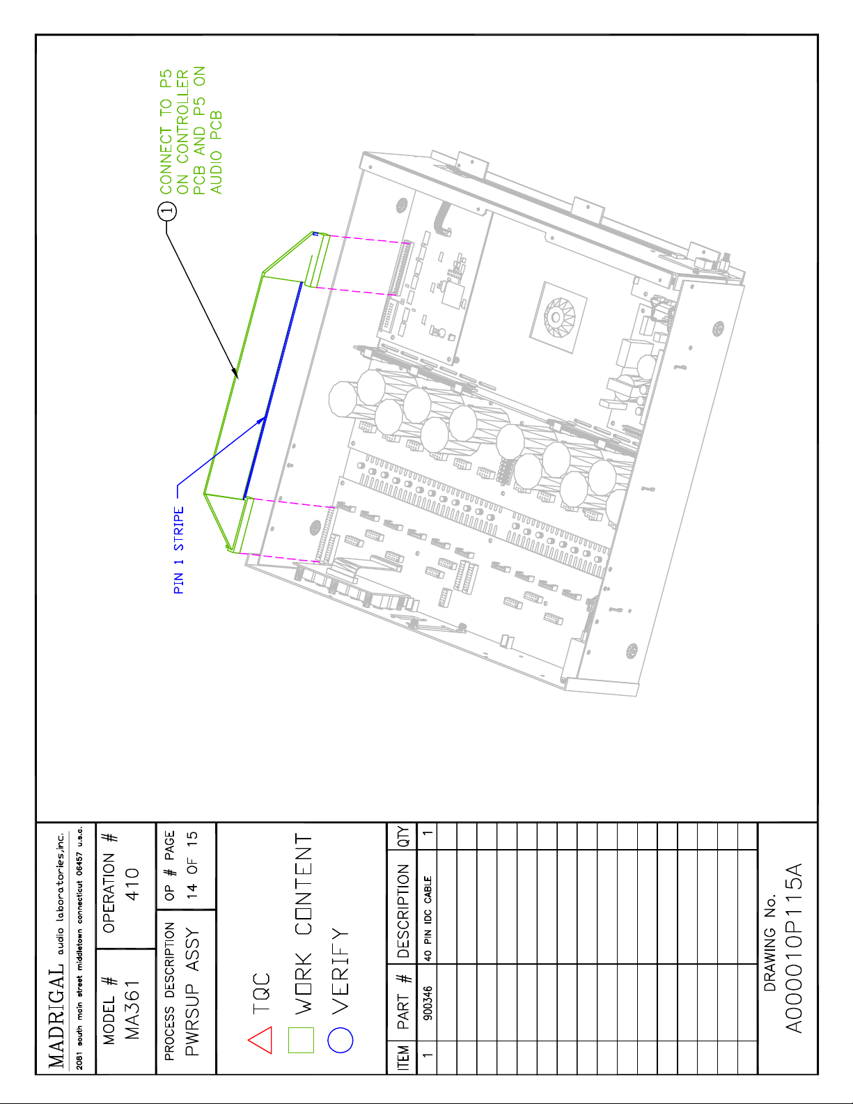
Step 18 Remove 40 Pin Ribbon Cable......................................................................................A000010P115A
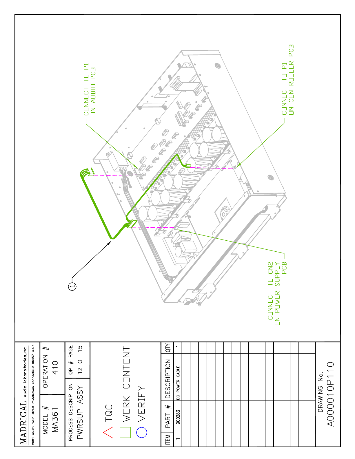
Step 19 Disconnect Connector on Audio Board P1.....................................................................A000010P110
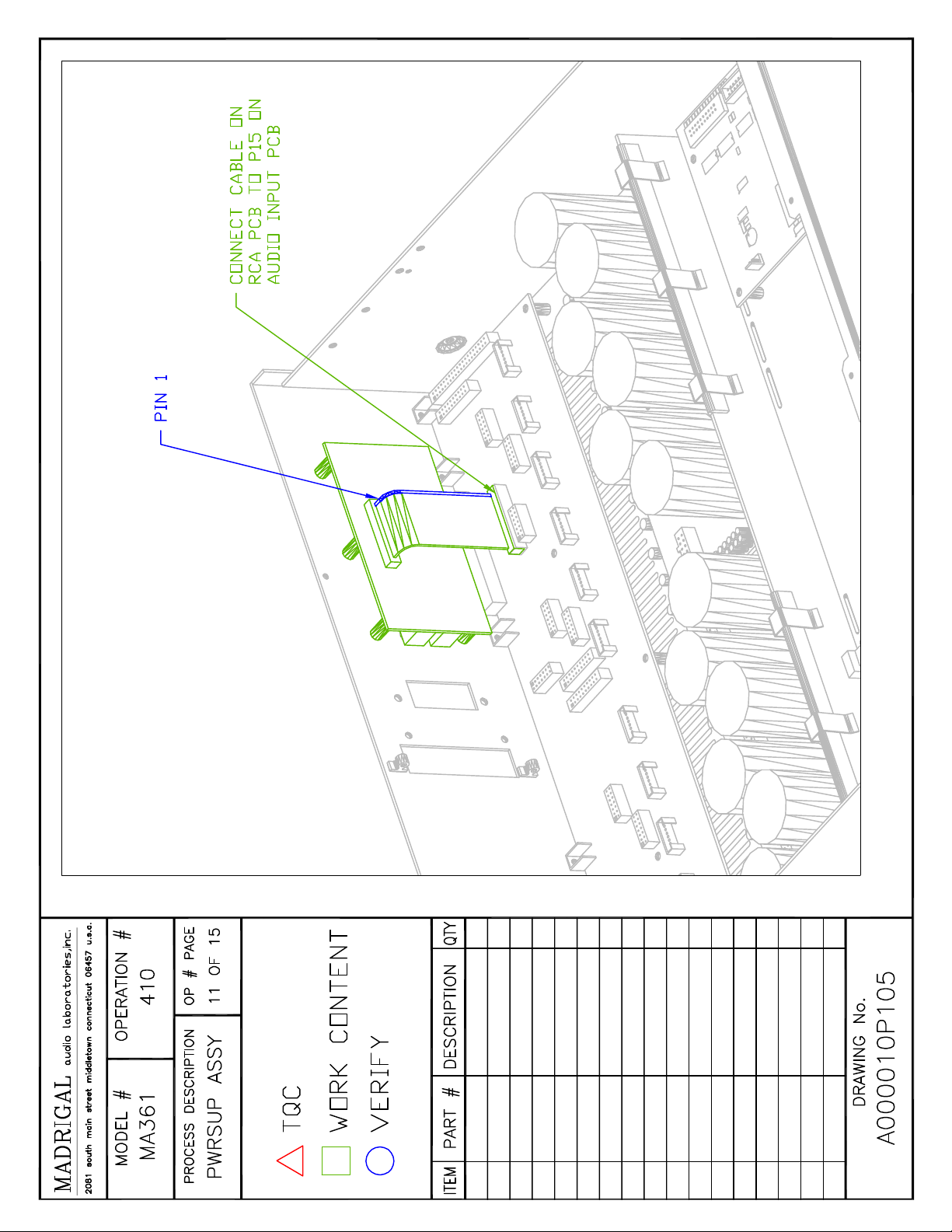
Step 20 Disconnect Cable on Audio Board to RCA Input Board .................................................... A000010P105
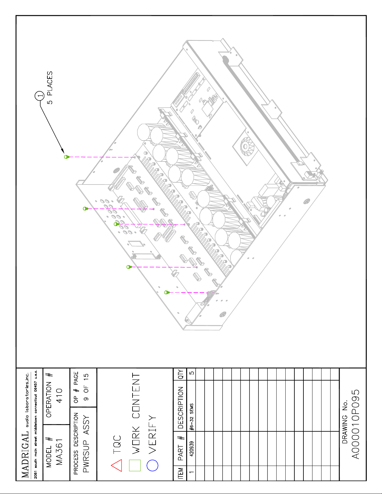
Step 21 Remove Screws on Audio Board1 ................................................................................. A000010P095
Step 22 Remove Back Panel Screws ......................................................................................... A000010P092
MA-361 Disassembly Instructions Page 2
Page 8
Audioaccess
APRIL 15, 2002 A041102
AUDIO BOARD DISASSEMBLY INSTRUCTIONS
Overview
The following procedure will allow a qualified Audioaccess Distributor to successfully remove and
reinstall the MA-361 Audio Board. New replacement audio boards shipped April 2002 eliminate a
problem where keypad messages may be heard as pops in Zones 1, 2 , 3 and 4 in affected units. In
addition, the signal sensing sensitivity was lowered to avoid audio from shutting off during low passages
of music if the amplifier is configured to turn on with Signal Sensing.
Affected Units
MA-361’s manufactured before the serial numbers listed below should receive an updated Audio Board.
Starting Serial Numbers
Updated Audio Boards
Domestic Units 361u1073
Export Units 361e1018
Cautions! Before Beginning
CAUTION!
Hazardous voltages available inside unit. Before proceeding, remove AC cable from
AC outlet.
CAUTION!
Static sensitive parts and subassemblies inside unit. A static protection wrist strap
must be worn when touch ing static sensitive components. Please follow wrist strap
manufacturers’ instructions for proper use.
Tools Required
o #2 Phillips Screwdriver
o 3/32” Hex Driver
o Needle Nose Pliers
MA-361 Disassembly Instructions Page 3
Page 9

Audioaccess
APRIL 15, 2002 A041102
AUDIO BOARD DISASSEMBLY INSTRUCTIONS
Disassembly/Reassembly Steps
The Disassembly steps are depicted in the process sheets and are identified below in Steps 1 through 22.
Instructions on each step are included in the process sheet for each step. In addition, some notes are provided below
to clarify a step for either Assembly or Reassembly.
Once the Audio Board has been extracted, repeat each step below in a backwards order from Step 22 through Step 1
when installing the replacement Audio Board.
Step Number Description Process Sheet Number
Step 1 Remove Top Cover.......................................................................................... A000010P265
Step 2 Remove Larger PCP Clamp Assembly .............................................................A000010P245
Step 3 Remove First Graphic EQ PCB ........................................................................A000010P210
Step 4 Remove Second Graphic EQ PCB ...................................................................A000010P205
Step 5 Remove Screws Holding RS -232/485 PCB .......................................................A000010P200
Step 6 Remove RS -232 PCB (CP Model Specific)........................................................A000010P190
This step is used for MA-361CP units only.
Step 7 Remove RS -485 PCB (Standard MA 361 Specific).............................................A000010P185
This step is used for the standard MA-361.
Step 8 Remove Amp Module Clamp Assembly ............................................................A000010P180
Note the “Dimples” or “Notches” on each end of the amp Clamp Assembly. When re -
installing this clamp, assure that these “dimples” are reinstalled in the same direction as
when removed.
Step 9 Remove Outer Ribbon to Audio Output PCB .....................................................A000010P170
Step 10 Remove Inner Ribbon to Audio Output PCB .......................................................A000010P165
Step 11 Remove Screws on Audio Output PCB ...........................................................A000010P160A
When reassembling, these screws must be tight for grounding purposes before AC
power is applied.
Step 12 Remove Audio Output PCB .............................................................................A000010P155
Step 13 Remove Audio Modules ...................................................................................A000010P150
Step 14 Remove Audio Module Signal Cables ...............................................................A000010P135
Step 15 Remove Audio Module Power Cables ...............................................................A000010P130
Step 16 Remove Volume Bypass Jumpers....................................................................A000010P125
These Jumpers are present whenever the Volume Tone Modules, EM401, are not used.
Remove these jumpers and install in the replacement Audio Board.
Step 17 Remove 20 Pin Ribbon Cable.........................................................................A000010P120A
Step 18 Remove 40 Pin Ribbon Cable.........................................................................A000010P115A
Step 19 Disconnect Connector on Audio Board P1........................................................A000010P110
Disconnect only the connector on the Audio Board PCB. Do not disconnect connector on
Power Supply or Controller PCB.
Step 20 Disconnect Cable on Audio Board to RCA Input Board .......................................A000010P105
Step 21 Remove Screws on Audio Board......................................................................A000010P095
Step 22 Remove Back Panel Screws ............................................................................A000010P092
MA-361 Disassembly Instructions Page 4
Page 10
Page 11
Page 12
Page 13
Page 14
Page 15
Page 16
Page 17
Page 18
Page 19
Page 20
Page 21
Page 22
Page 23
Page 24
Page 25
Page 26
Page 27
Page 28
Page 29
Page 30
Page 31

Page 32

MA361/M361CP
Electrical/Mechanical Parts Lists
Note:
These parts lists may contain some part
numbers that are not valid, or No Longer
Available.
Descriptions and Reference Designators,
when included, should aid technicians in part
substitution.
If necessary, call the Parts department at
1-516-496-3400 ext. 6553 for assistance.
Page 33

MA-361 MAIN PARTS LIST
r
r
-
9
R
A
R
7
3
A
8
0
A
8
-
8
A
2
T
7
r
r
4
A
6
Part Numbe
CAP LYTIC 47U 20% 16V SMT PAN. EEV
200256
760225
327-01009-00 CONN D_SUB 9PIN PCMT 745781-4 9PIN FEM
220189 CAP EMI 10N 30% 50V RADIAL PAN. EXC-
23010
205-70200-00 DIODE, TVS, 600W, UNI-DIR, 20V, SMT
320-50003-00 SAMTEC HEADER 2X
320-59902-00 SHUNT JUMPER 1X2
E01535
33070
612-18190-00 BRACKET, PC MNT SCREW TERM, 8190 (NO
580646
HB1C470 1 PANASONIC-EEV-HB1C470
C2
ICS DIG ADM202EARN RS232 DRV/RCVR
SMD 1 ANALOG DEVICES-ADM202JRN
U1
DS
P1
CET103
DF1 DF2
CAP SMD .1UF 25V X7R CE
C1 C3 C4 C5 C6 C
ESD1 ESD2
P3
P3
CONN HEADER 14PIN PCMT TSW-107-08-T-D
RA .1SP D/R R/A 1 SAMTEC TSW-107-08-T-D-RA NO GOLD!
P1
SCREW)
MT1 MT2
PCB MA361 RS23
Description QTY Manufacture
Comments
1 AMP- 745781-4 USED IN PX700
2 PANASONIC-EXC-CET103
6
2 MOTOROLA- 1SMB20AT3 MFG'S P/N CORRECTED
1 SAMTEC- TSW-103-07-G-D
2 3M- 929950-0
2
1 PER DWG# 943320B DRILL CHAR
NY MANUFACTURE
DDED- ECN300
DDED- ECN300
INSTALL IN DTE
POSITION-
PER REVISED ASS'Y
DWG 943321B- ECN3105
KEYSTONE- 8190 NO SCREW
WAS 580646- ECN300
BD FILENAME: 580646A.ZIP
Part Numbe
10077
RES SMT 330R 5% 1/10W 0805 14
R1 R10 R13 R14 R15 R16 R2 R3 R4 R5 R
R7 R8 R9
Description QTY Manufacture
NY APPROVED
Comments
Page 34

230145 CAP CER_X7R 100N 5% 50V SMT 0805 14 ANY APPROVED
A
6
6
5
-
A
2
A
A
P
r
6
A
R
8
C1 C4 C7 C10 C13 C16 C19 C22 C25 C28
C31 C34 C37 C40
230150 CAP CER_X7R 1N0 5% 100V SMT 0805 28
C11 C12 C14 C15 C17 C18
C2 C20 C21 C23 C24 C26 C27
C29 C3 C30 C32 C33 C35 C36
C38 C39 C41 C42 C5 C6
C8 C9
310101 WIR 26 COND FLAT RIBBON GREY 3 AMPHENOL- 843-191-2801-126
330337 CON LNMT 26PIN .1SP SOCKET IDC 1 AMP- 2-216408-6
330339 CON PCMT 26PIN .1SP DIP PLUG W/ LEGS 1 AMP- 111382-6
CONN RCA_F 3PIN PCMT RCA-151R-G RED
E01610
33016
E01611
33016
E01631
580656
VERT MT RCA 7 Power Dynamics- 151W-G Gold plated
P10 P12 P14 P2 P4 P6 P8
CONN RCA_F 3PIN PCMT RCA-151W-G
WHITE VERT MT RCA 7 Power Dynamics- 151R-G Gold plated
P1 P11 P13 P3 P5 P7 P9
P15
MISC SWAGE 156 SWAGE 9/16"L RAF 3052-B
632-B-37 6 RAF 3052-B-632-37
MT1 MT2 MT3 MT4 MT5 MT6
PCB, RCA INPUT PX71
ANY APPROVED
MPHENOL- 843-191-2801-02
1 TBD
1
S PER DWG# 943350
BD ARTFILENAME- 580656A.ZI
C1, C4, C7, C10, C13,
C16, C19, C22, C25, C28
C31, C34, C37, C40
ADDED- ECN3043
C1, C4, C7, C10, C13,
C16, C19, C22, C25, C28
C31, C34, C37, C40
REMOVED- ECN3043
For RCA to Audio cable per
dwg# C000024
For RCA to Audio cable per
dwg# C000024
For RCA to Audio cable per
dwg# C000024
P/N Description QTY Manufacture
10050
RES SMT 22K1 1% 1/10W 0805 6
R1138 R338 R38 R538 R738 R93
NY MANUFACTURE
Comments
Page 35

10050
9
A
R
9
A
R
3
8
9
2
A
R
3
4
A
R
0
3
A
R
8
6
6
RES SMT 4K99 1% 1/10W 0805 1
NY MANUFACTURE
R1224
100543 RES SMT 10M 1% 1/10W 0805 12 ANY MANUFACTURER
10054
RES SMT 221R 1% 1/10W 0805 6
NY MANUFACTURE
R1133 R33 R333 R533 R733 R93
100584 RES SMT 1K00 1% 1/10W 0805 34
ANY MANUFACTURER
R1117 R1118 R1139 R1301 R1303 R1305
R1307 R1309 R1311 R17 R18 R317 R31
R339 R39 R42 R44 R46 R47 R517 R518
R539
R717 R718 R739 R917 R918 R93
R41, R341, R541, R741, R941, R1141
10076
RES SMT 47K0 5% 1/10W 0805 6
NY MANUFACTURE
R1013 R1213 R213 R413 R613 R81
10077
RES SMT 330R 5% 1/10W 0805 8
NY MANUFACTURE
R1315 R1316 R1317 R1318 R1319 R132
R43 R45
10078
RES SMT 3K32 1% 1/10W 0805 15
NY MANUFACTURE
R1001 R1026 R1201 R1225 R1226 R122
R1229 R201 R226 R401 R426 R601 R62
R801 R82
100787 RES SMT 20K0 1% 1/10W 0805 106
ANY MANUFACTURER
R1 R10 R11 R1105 R1106 R1107 R1108
R1109
R1110 R1111 R1112 R1113 R1114 R1119 R1125 -ECN3104
R1120 R1122 R1123 R1124
R1126 R1127 R12 R13 R14 R19 R2 R20
R22 R23 R24 R26 R27 R3 R305 R306
R307 R308 R309 R310 R311 R312 R313
R314
R319 R320 R322 R323 R324 R326
R327 R4 R5 R505 R506 R507 R508 R509
R510 R511 R512 R513 R514 R519 R520
R522 R523 R524 R526 R527 R6 R7
R705 R706 R707 R708 R709 R710 R711
R712
ADDED R31, R32, R331,
R332, R531,
R532, R731, R732, R931,
R932,
R1131, R1132- ECN3104
ADDED R41, R341, R541,
R741, AND
R941, R1141- WERE
E01501
ECN3104
REMOVED R21, R25,
R321, R325, R521,
R525, R721, R725, R921,
R925, R1121,
Page 36

R713 R714 R719 R720 R722 R723 R724
9
A
R
7
0
6
1
7
7
8
2
-
8
R726 R727 R8 R9 R905 R906 R907
R908 R909 R910 R911 R912 R913 R914
R919
R920 R922 R923 R924 R926 R927
10078
RES SMT 100K 1% 1/10W 0805 12
R1002 R1027 R1202 R1227 R202 R227 R402
R427 R602 R627 R802 R82
100820 RES SMT 10K0 1% 1/10W 0805 103
R1005 R1006 R1007 R1008 R1009 R1010
R1012 R1014 R1015 R1115 R1135 R1140
R1205 R1206 R1207 R1208 R1209 R121
R1212 R1214 R1215 R1302 R1304 R130
R1308 R1310 R1312 R1313 R1314 R132
R1322 R1323 R1324 R1325 R1326 R132
R1328 R1329 R1401 R15 R205 R206 R20
R208 R209 R210 R212 R214 R215 R315
R335
R340 R35 R36 R40 R405 R406 R407 R40
R409 R410 R412 R414 R415 R515 R535
R540
R605 R606 R607 R608 R609 R610 R612
R614
R615 R715 R735 R740 R805 R806 R807
R808
R809 R810 R812 R814 R815 R915 R935
R940
NY MANUFACTURE
ANY MANUFACTURER
ADDED R21, R25, R321,
R325, R521,
R525, R721, R725, R921,
R925,
R1121, R1125- WERE
100787- ECN3104
R21 R25 R321 R325 R521 R525 R721 R725
R921 R925 R1121 R1125
E01755
CAP LYTIC 2U2 20% 35V SMT TANT PAN.
ECS
C1302 C1304 C1306 C1308 C1310 C131
6
PANASONIC- ECS-H1VC225R
WAS 200246 (PANASONICECS-HIAC106R
ECN3104
CAP LYTIC 47U 20% 16V SMT PAN. EEV
200256
HB1C470P 22 PANASONIC- EEV-HB1C470P
C1118 C1120 C1135 C18 C2 C20 C318 C320
C335 C35 C42 C45 C518 C520 C535 C71
Page 37

5
23010
9
5
A
R
6
2
7
7
9
3
2
8
4
0
6
2
2
1
1
C720 C735 C8 C918 C920 C93
CAP CER_X7R 100N 10% 25V SMT 080
C1 C10 C1001 C1002 C1003 C1004 C100
C1007 C1008 C1009 C1010 C1011 C101
C1014 C1109 C1110 C1112 C1113 C111
C1119 C1121 C1122 C1123 C1126 C112
C1130 C1131 C1138 C1139 C12 C1201
C1202
C1203 C1204 C1206 C1207 C1208 C120
C1210 C1211 C1214 C1215 C1216 C13
C1301
C1303 C1305 C1307 C1309 C1311 C131
C1314 C1315 C1316 C1317 C1401 C140
C1403 C1404 C1405 C1406 C1407 C140
C1409 C1410 C1411 C1412 C1413 C141
C1415 C1416 C1417 C1418 C1419 C142
C1421 C1422 C1423 C1424 C1425 C142
C1427 C1428 C1429 C1430 C1431 C143
C1433 C1434 C1435 C1436 C1501 C150
C1503 C1504 C17 C19 C201 C202 C203
C204
C206 C207 C208 C209 C21 C210 C211 C212
213
NY MANUFACTURE
C214 C22 C23 C26 C27 C30 C309 C31 C310
C312 C313 C317 C319 C321 C322 C323
C326
C327 C330 C331 C338 C339 C36 C4 C40
C402 C403 C404 C406 C407 C408 C409 C41
C410 C411 C43 C44 C46 C5 C509 C510
C512
C513 C517 C519 C521 C522 C523 C526
C527
C530 C531 C538 C539 C601 C602 C603
C604
C606 C607 C608 C609 C610 C611 C612
C614
C7 C709 C710 C712 C713 C717 C719 C72
C722 C723 C726 C727 C738 C739 C801
C802
C803 C804 C806 C807 C808 C809 C810
C811
Page 38

C9 C909 C910 C912 C913 C917 C919 C92
1
3
5
3
6
-
2
D
2
4
7
2
A
R
3
3
C922 C923 C926 C927 C930 C931
CONN HEADER 26PIN PCMT mtsw-113-08-S-D
330707
70012
72002
720138
780214 IC LINEAR TL072CD DUAL OP AMP SOIC 31 Texas Instrument- TL072CD
78029
340 .100" 1 SAMTEC TSW-113-07-T-D
P15
DIODE MMBD914 SILICON SMT 1N914 30 MOTOROLA- MMBTD914LT1
CR1103 CR1104 CR1105 CR1301 CR1302
CR1303
CR1304 CR1305 CR1306 CR1307 CR1308
CR1309
CR1310 CR1311 CR1312 CR3 CR303 CR304
CR305 CR4 CR5 CR503 CR504 CR505
CR703
CR704 CR705 CR903 CR904 CR90
DIODE 4N33 OPTO OPTO COUPLER 6 QT TECHNOLOGIES- 4N33
U1301 U1302 U1303 U1304 U1305 U130
XISTOR MMBD3904LT1 NPN UNSORT SMD
2N3904 25 MOTOROLA- MMBD3904LT1
Q1 Q1002 Q1003 Q1005 Q1102 Q1202
Q1203
Q1205 Q1401 Q202 Q203 Q205 Q302 Q402
Q403 Q405 Q502 Q602 Q603 Q605 Q702
Q802
Q803 Q805 Q902
U1 U1102 U1104 U1105 U1106 U1107 U
U302 U304 U305 U306 U307 U4 U5 U50
U504 U505 U506 U507 U6 U7 U702 U70
U705 U706 U707 U902 U904 U905 U906
U907
IC INA117KU ANA DIF AMP 12 BURR BROWN- INA117KU
Motorola- TL072C
WAS LM358 (780158)
ECN3023
U1001 U1002 U1201 U1202 U201 U202 U401
U402 U601 U602 U801 U80
320-55010-00
E00502 RES SMT 33K2 1% 1/10W 0805 24
CONN HEADER 20PIN PCMT 102618-8 .1 2
ROW SHD 3
P3 P4 P6
R1018 R1023 R1128 R1129 R1218 R122
R218 R223 R28 R29 R328 R329 R418 R42
AMP 103309-5
NY MANUFACTURE
Page 39

R528 R529 R618 R623 R728 R729 R818
9
-
2
6
8
4
4
R
7
R823
R928 R92
CAP LYTIC 1U0 20% 50V SMT PA. EEV
E00580
E01023 RES SMT NU 1% 1/10W 0805 6 NOT USED
E01106 XISTOR MMBT3906 PNP SMD 2N3906 18
E01181
E01346
100545 RES SMT 49R9 1% 1/10W 0805 1 ANY MANUFACTURER
E01503 CAP CER 18P0 10% 50V SMT 0805 62 ANY MANUFACTURER
HA1H010R 6 PANASONIC-EEV-HA1H010R
C1132 C32 C332 C532 C732 C93
R1116 R16 R316 R516
R716 R916
ON SEMICONDUCTOR-
MMBT3906LT1
Q1001 Q1004 Q1103 Q1201 Q1204 Q2 Q201 DIODES INC- MMBT3906-7
Q204 Q303 Q401 Q404 Q503 Q601 Q604
Q703
Q801 Q804 Q903
DIODE LSS269-BO LED DO NOT USE
OBSOLETE 6 LEDTRONICS- SML 10R3-TR
LED1 LED2 LED3 LED4 LED5 LED
IC SN74LVC573ADW DIG SMT OCTAL
LATCH 2
U1307 U130
R37
C1005 C1013 C11 C1111 C1114 C1115
C1116 C933, C1133- ECN3104
C1124 C1125 C1128 C1129 C1205
C1213 C14 C15 C16 C205 C213 C24 C25
C28 C29 C3 C311 C314 C315 C316 C324
C325 C328 C329 C405 C413 C511
C514 C515 C516 C524 C525 C528 C529
TI- CD74HC573M
R31, R32, R331, R332,
R531,
R532, R731, R732, R931,
R932,
R1131, R1132 are 10M
(100543)
WAS 180R (E01395)ECN310
REMOVED C33,C333,
C533, C733,
E0153
C6 C605 C613 C711 C714 C715 C716 C724
C725 C728 C729 C805 C813 C911 C914
C915 C916 C924 C925 C928 C929
DIODE BZX84C5 ZENER 5.1V ZENE
4 DIODES INC- BZX84C5V1-
Page 40

CR1 CR1203 CR1204 CR
2
6
M
3
8
9
3
A
R
7
6
2
L
R
9
A
R
4
7
612-18190-00
MISC HOLE 6-32 R/A SCREW TERMINAL 5 KEYSTONE- 8190
M10 M11 M7 M8 M9
E0163
IC CD4016BCM DIG QUAD SWITCH 3 FAIRCHILD- CD4016BC
U3 U503 U90
E0163
IC LM339AM ANA QUAD COMP 9 NAT'L SEMICONDUCTOR- LM339AM
U1004 U1005 U1204 U204 U205 U404 U604
U605 U804
E0163
IC LM324AM ANA QUAD OPAMP 6 NAT'L SEMICONDUCTOR- LM324AM
U1003 U1203 U203 U403 U603 U80
E01641 RES SMT 475K 1% 1/10W 0805 24
R1016 R1017 R1021 R1022 R1216 R121
R1221 R1222 R216 R217 R221 R222 R41
R417 R421 R422 R616 R617 R621 R622
R816
R817 R821 R82
CONN HEADER 8PIN PCMT B8B-PH-KL JST
E01644
.079 CTR 12 JST- B8B-PH-KL
P1L P1R P2L P2R P3L P3R P4L P4R P5
P5R P6L P6
CONN HEADER 4PIN PCMT 22-27-2041
E01645
MOLEX .1SP LOCKING 1 MOLEX- 22-27-2041
P1
CONN HEADER 12PIN PCMT 861912 MOLEX
E01646
5.08MM R/A 1 MOLEX- 861912
P2
CONN SOCKET 14PIN PCMT .1SP D/R
E01647
SOCKET 11 AMP 534998-7
NY MANUFACTURE
P10 P11 P1V P2V P3V P4V P5V P6V P7 P8
P9
E0164
RES SMT 1M50 1% 1/10W 0805 6
NY MANUFACTURE
R1134 R334 R34 R534 R734 R93
TOSHIBA- 2SC3326-B
NOT USED NOT USED 0
do not populate- ECN3023
Q3 Q4
E01651 CAP LYTIC 4U7 20% 16V SMT SMCAP4X4_3 6 PANASONIC- ECEV1CA4R7NR
C1137 C337 C37 C537 C737 C93
E01696
CONN HEADER 40PIN PCMT TST-120-01-T-D
D/R SHROUDED CABLE HDR 1
AMP 103309-8
P5 SAMTEC TST-120-01-T-D
Page 41

SWITCH THERMAL 70 DEGREES C
4
r
R
5
5
ANY
r
r
A
R
5
A
R
6
A
4
A
8
A
8
-
5
0
5
-
2
E01747
ENCAPSULATED THERMOSTAT
2 CANTHERM F11070151ZA0060 WAS- E01697- ECN
S1 S2 normally open- w/ NO PC Pins
CAP LYTIC NOT 20% USED SMT
E01700
SMCAP4X4_3 NU 6 NOT USED DO NOT INSTALL
C1134 C334 C34 C534 C734 C93
580643B PCB, AUDIO MA-361 1 PER DRILL CHART#943311B WAS 580643A- ECN3104
BD ART FILE- 580643B.ZIP
Part numbe
23014
CAP SMD .1UF 50V 10% CER X7R 080
Description QTY MANUFACTURE
24
C1-24
Part Numbe
100511 RES SMT 7K50 1% 1/10W 0805 12
Description QTY Manufacture
NY MANUFACTURE
R1 R201 R203 R204 R205 R3 R301 R303
R304 R305 R4 R5
100561 RES SMT 1M00 1% 1/10W 0805 6
NY MANUFACTURE
R2 R202 R206 R302 R306 R
100765 RES SMT 1K00 5% 1/10W 0805 7 ANY MANUFACTURER
R10 R209 R210 R309 R310 R9 R40
100774 RES SMT 330R 5% 1/10W 0805 6 ANY MANUFACTURER
R207 R208 R307 R308 R7 R
100547 RES SMT 0R00 5% 1/10W 0805 6 ANY MANUFACTURER
C9 C2 C209 C202 C309 C30
CAP LYTIC 47U 20% 16V SMT PAN. EEV
200256
HB1C470P 14 PANASONIC EEV-HB1C470P
C203 C205 C242 C24
C3 C303 C305 C342 C345 C41
C412 C42 C45 C
CAP PESTR_FILM 2N2 5% 100V RADIAL FKP
220047
2 6 WIMA- FKP2, 2200PF 100V 5%
C18 C218 C232 C318 C32 C33
COMMENTS
Comments
R304 R305 R4 R
Ref des on wrong line,
restored
DDED
R9,10,209,210,309,310
REMOVED
R7,8,207,208,307,308
DDED
R7,8,207,208,307,308
DDED C9 C2 C209 C202
C309 C308
REMOVED C1 C10 C201
C210 C01 C310
Page 42

220065 CAP PESTR_FILM 68N 5% 63V RADIAL MKS-2 6 WIMA- MKS2 .068UF 63V 5%
9
4
6
3
7
5
3
7
9
6
4
4
0
5
5
A
R
5
6
5
A
R
8
C17 C217 C231 C31 C317 C331
CAP PESTR_FILM 150N 5% 50V RADIAL
220076
WIMA MKS-02 6 WIMA- MKS02, .15UF, 50V, 5%
C15 C215 C229 C29 C315 C32
CAP PESTR_FILM 1N5 10% 63V RADIAL
220105
MKS02 3 WIMA- MKS02 1500PF, 63V, 10%
C224 C24 C32
220107 CAP PESTR_FILM 33N 5% 63V RADIAL MKS2 6 WIMA- MKS2, .033UF 63V 5%
C12 C212 C226 C26 C312 C32
220108 CAP PESTR_FILM 22N 5% 63V RADIAL MKS2 6 WIMA- MKS2, .022UF, 63V, 5%
C19 C219 C233 C319 C33 C33
CAP PESTR_FILM 330N 5% 63V RADIAL
220117
MKS2 6 WIMA- MKS2, .33UF, 63V, 5%
C13 C213 C227 C27 C313 C32
220119 CAP PESTR_FILM 1U0 5% 63V RADIAL MKS2 6 WIMA- MKS2 1UF 63V 5%
C11 C211 C225 C25 C311 C32
220121 CAP PESTR_FILM 3N3 5% 63V RADIAL FKP-2 12 WIMA- FKP2, 3300PF 63V 5%
C22 C222 C223 C23 C236 C237 C322 C32
C336 C337 C36 C3
230109 CAP CER_X7R 100N 10% 25V SMT 0805 32 ANY MANUFACTURER
C204 C206 C207 C208 C23
C240 C241 C243 C244 C246 C304 C30
C307 C308 C339 C340 C341 C343 C34
C346 C39 C4 C40 C41 C411 C413 C43 C4
C46 C6 C7 C8
CAP LYTIC NOT 20% USED SMT
E01707
SMCAP6_3X6_6 6 ANY MANUFACTURER NOT USED
C1 C10 C201 C210 C01 C31
23011
CAP CER_X7R 10N 10% 100V SMT 080
6
NY MANUFACTURE
C21 C221 C235 C321 C335 C3
23014
CAP CER_NPO 15N 5% 50V SMT 080
6
NY MANUFACTURE
C14 C214 C228 C28 C314 C32
780214 IC LTL072CD DUAL OP AMP SOIC 3 Fairchild- TL072CD
U1 U201 U301 Motorola- TL072CD
REMOVED FOR
RESISTORS C9 C2 C209
C202 C309 C308
was National LM358ADR-
ECN3023
Page 43

145-400011
0
5
A
R
8
4
R
7
2
-
8
6
5
A
R
0
7
5
A
R
4
2
r
r
2
6
9
4
A
R
6
S
R
9
-
9
R
A
R
4
3
5
A
5
7
CAP CER_X7R 1N5 5% 50V SMT 080
3
NY MANUFACTURE
C238 C338 C3
E0153
DIODE BZX84C5 ZENER 5.1V ZENE
6 DIODES INC- BZX84C51 CR1 CR2 CR201 CR202 CR301 CR30
CONN HEADER 14PIN PCMT TSW-107-08-T-D
E01535
33070
E0161
RA .1SP D/R R/A 2 SAMTEC- TSW-107-08-T-D-RA NOT GOLD
P401 P402
CAP CER_X7R 6N8 10% 50V SMT 080
6
NY MANUFACTURE
C16 C216 C230 C30 C316 C33
E0167
CAP CER_NPO 820P 5% 50V SMT 080
6
NY MANUFACTURE
C20 C220 C234 C320 C334 C3
760176 IC LC7527E DIG 7B GRAPHIC CTRLR 3 SANYO LC7527E Special pin 1 placement!!!!
U2 U202 U30
580662A PCB MA361 GEQ2 BD 1 AS PER DWG# 943377A DRILL CHT.
580662A.ZIPBD ART FILE
Part Numbe
Description QTY Manufacture
100755 RES SMT 10K0 5% 1/10W 0805 18 ANY MANUFACTURER
R1 R10 R11 R12 R13 R14 R15 R17 R
R20 R22 R3 R4 R5 R6 R7 R8 R
10077
RES SMT 330R 5% 1/10W 0805 2
NY MANUFACTURE
R18 R19
CAP LYTIC 330U 20% 25V RADIAL NICHICON
200206
20024
PL/PM SERIES
C1
CAP LYTIC 10U 20% 10V SMT PAN. EC
1 NICHICON- UPL1E331MPH
NICHICON- UPM1E331MPH
7 PANASONIC-ECSH1AC106
C12 C15 C17 C22 C3 C7 C
CAP EMI 10N 30% 50V RADIAL PAN. EXC
220189
CET103U 1 PANASONIC- EXC-CET103U
DF1
23010
CAP SMD .1UF 25V X7R CE
12
NY MANUFACTURE
C13 C14 C16 C18 C19 C2 C20 C21 C23 C
C6 C8
33042
CONN HEADER 10PIN PCMT 102973-
1
MP- 102973P7
Comments
R16 REMOVED. DO NOT
POPULATE
ECN303
UPM series cap
equivalent added
ECN3138
WAS 330137- ECN300
Page 44

70012
3
2
5
3
5
A
R
4
8
0
6
A
R
3
A
R
6
C
T
B
2
A
7
r
R
DIODE MMBD914 SILICON SMT 1N914 1 MOTOROLA- MMBD914LT1
CR3 DIODES INC
230-30574-00 D FLIP FLOP, OCT 3STATE, 74HC574, SMT
U4 U5 U6 U7 U8
320-55010-00 HEADER, 2X10, SHROUDED
P4
CONN HEADER 14PIN PCMT TEST .1"SP D/R
E01133
TPO 1 ANY MANUFACTURER
P6 PROTO USE ONLY
DIODE LSS269-BO LED SMT RED
E01181
71003
1.8V@2mA 2 LEDTRONIICS SML 10R3-TR
LED1 LED2
CONN HEADER 2PIN PCMT MOLEX 2PIN .1
E01311
SP LOCKING 22-27-2021 1 MOLEX- 22-27-2021
P1
230-30573-00 LATCH, OCTAL, TRI STATE, 74HC573, SMT
U2 U3
E0150
CONN 5PIN B-5B-PH-K-S JST 2MM 1 JST- B-5B-PH-K-S
P3
E0150
CAP CER 18P0 10% 50V SMT 080
C10 C11
E0150
76017
IC COP8SBR9HVA8 MEM MPU 1 NATIONAL- COP8SBR9HVA
U1
CONN HEADER 40PIN PCMT TST-120-01-T-D
E01XXX
.1SP SHROUDED SAMTEC 1 SAMTEC- TST-120-01-T-D NOT GOLD
P5
MISC CRYSTAL 9.216MHZ
E01509
81005
HC49US9.216MABJ 1 CITIZEN- HC49US9.216MABJ
X1
E01512 RES SMT 50R0 5% 1/10W 0805 1
R21
E0151
RES SMT 1M00 5% 1/10W 0805 1
R23
33074
CON PCMT 44PIN SOCKET PLC
U1
580642
PCB, CONTROLLER, PX71
TEXAS INSTRUMENTS-
5
CD74HC574M
1
AMP- 103309-5
TEXAS INSTRUMENTS-
2
CD74HC573M
2
NY MANUFACTURE
NY MANUFACTURE
NY MANUFACTURE
1 MACKENZIE- PLCC44P-
1
S PER DRILL DWG# 943308B WAS 580642A- ECN300
BD ART FILE- 580642B.ZIP
EMULATOR
CONNECTION
Part numbe
Description QTY MANUFACTURE
COMMENTS
On solder side from pin 4
100111 RES 20R0 RN55D 1% MTL FLM AXIAL 1 DALE OR ANY MANUFACTURER
(P1) to Ground plane.
Page 45

R4 ECN308
8
-
-
9
R
A
R
XCVR
-
A
P
r
r
6
A
R
A
R
2
A
R
4
A
R
3
A
R
CAP LYTIC 47U 20% 16V SMT PAN. EEV
200256
HB1C470 1 PANASONIC-EEV-HB1C470
C1
100584 RES SMD 1K 1% 1/10W 0805
R2
700150
DIODE, TVS, 600W, BI-DIR, 11.0V, SMT 2 On Semi- P6SMB11CAT3
ESD1 ESD2
220189 CAP EMI 10N 30% 50V RADIAL PAN. EXC-
CET103
DF1 DF2
23010
CAP SMD .1UF 25V X7R CE
C2 C3
760279 IC MAX485ECSA DIG +15KV ESD RS485
U1
323-00004-00 CONN, TERM BLK, PLG, PCRA, 4 PIN
P1
CONN HEADER 14PIN PCMT TSW-107-08-T-D
320-50107-00
RA .1SP D/R R/A 1 SAMTEC-TSW-107-08-T-D-RA
P2
612-18190-00 BRACKET, PC MNT SCREW TERM, 8190 (NO
SCREW)
MT1 MT2
580647A PCB RS485 MA361 1
MA361 VOLUME CONTROL BD ASS'Y
1 ANY MANUFACTURER
2 PANASONIC-EXC-CET103
2
NY MANUFACTURE
1 MAXIM- MAX485ECSA
1
WIELAND-25.332.3453.1
KEYSTONE- 8190
2
S PER DWG# 943323B- DRILL
CHART WAS 580647- ECN3007
BD FILENAME- 580647A.ZI
WAS 120R (122-31120-00)
ECN3088
Replaces 205-70050-00ECN3151
WAS 760146 (LINEAR
TECH-LTC485CS8)ECN3298
Part Numbe
10054
Description QTY Manufacture
RES SMT 330K 5% 1/10W 0805 2
NY MANUFACTURE
COMMENTS
R24 R7
100561 RES SMT 1M00 1% 1/10W 0805 1
NY MANUFACTURE
R8
10076
RES SMT 47K0 5% 1/10W 0805 2
NY MANUFACTURE
R14 R18
10076
RES SMT 10K0 5% 1/10W 0805 1
NY MANUFACTURE
R27
100765 RES SMT 1K00 5% 1/10W 0805 4 ANY MANUFACTURER R28 ADDED- ECN3023
R1 R2 R26 R28
10077
RES SMT 10R0 5% 1/10W 0805 3
NY MANUFACTURE
Page 46

R3 R4 R5
4
A
R
3
A
R
9
A
R
-
5
9
5
3
A
R
9
6
5
A
R
-
A
R
A
R
3
5
A
R
A
R
5
5
A
R
6
5
A
R
7
5
A
R
8
5
A
R
A
R
10077
RES SMT 330R 5% 1/10W 0805 2
NY MANUFACTURE
R25 R6
10078
RES SMT 3K32 1% 1/10W 0805 2
NY MANUFACTURE
R15 R16
10078
RES SMT 100K 1% 1/10W 0805 2
NY MANUFACTURE
R13 R17
CAP LYTIC 47U 20% 16V SMT PAN. EEV
200256
HB1C470 8 PANASONIC
C11 C16 C17 C2 C29 C32 C35 C
23010
CAP CER_X7R 100N 10% 25V SMT 080
C1 C10 C13 C14 C15 C18 C24 C3 C30 C3
17
NY MANUFACTURE
C34 C36 C4 C6 C7 C8 C
23014
CAP CER_NPO 15N 5% 50V SMT 080
2
NY MANUFACTURE
C22 C26
780214 IC TL072CD DUAL OP AMP SOIC 1 Texas Instrument- TL072CD
U3 Motorola- TL072CD
XISTOR MMBD3904LT1 NPN UNSORT SMD
720138
2N3904 1 ANY MANUFACTURER
Q1
121-31150-00 RES, SMT, 1.50K, 1%, TF, 1/8W, 0805
2
NY MANUFACTURE
R10 R21
121-30681-00 RES, SMT, 681, 1%, TF, 1/8W, 0805
2
NY MANUFACTURE
R12 R22
E0150
CAP CER 18P0 10% 50V SMT 080
2
NY MANUFACTURE
C12 C31
122-35100-00 RES, SMT, 1M, 5%, TF, 1/8W, 0805
1
NY MANUFACTURE
R23
E0152
CAP CER_NPO 180N 10% 50V SMT 080
1
NY MANUFACTURE
C27
E0152
CAP CER_NPO 3N9 10% 50V SMT 080
2
NY MANUFACTURE
C19 C28
E0152
CAP CER_NPO 68N 10% 50V SMT 080
2
NY MANUFACTURE
C23 C25
E0152
CAP CER_NPO 18N 10% 50V SMT 080
1
NY MANUFACTURE
C20
224-09184-00
IC TC9184AP ANA TONE CONTROL 1 TOSHIBA- TC9184AP
U2
224-33310-00
IC CS3310KS CONV STEREO VOL CTRL 1 CRYSTAL SEMI
U1
121-32147-00 RES, SMT, 14.7K, 1%, TF, 1/8W, 0805
2
NY MANUFACTURE
R20 R9
NOT NPO
was 780158 (LM358ADR)
ECN3023
NOT NPO
NOT NPO
NOT NPO
Page 47

121-33127-00 RES, SMT, 127K, 1%, TF, 1/8W, 0805
A
R
4
R
-
A
2
A
R11 R19
E0153
330708
580648
DIODE BZX84C5 ZENER 5.1V ZENE
CR1 CR2 BZX84C5V1
CONN HEADER 14PIN PCMT TSW-107-08-T-D
RA .1SP D/R R/A 1 SAMTEC TSW-107-08-T-D-RA NO GOLD!
P1
PCB, VOLUME-TONE PX71
MA361 PARTS LIST
ICE MODULE ASSEMBLY
2
2 ZETEX-DIODES INC
1 DRILL CHART- 943326
NY MANUFACTURE
BD ART- 580648A.ZIP
80A-00070-00
420904
420815
430432
501778J-3
900274
900306
900332
770538
760170
600297
600298
600299
ICE MODULE ASSEMBLY
HDW SCR PAN HD PH 6-32 X .375
HDW SCR PAN HD PH POSI M3 X .5 (2)
MISC MECH MA361 ICE MODULE FOA
METAL MA361 LOWER ICE BRACKET
OEM PART ICE250A-IC MODULE
AUDIO INPUT BOARD ASSEMBLY
RS485 BOARD ASSEMBLY
V1.04 SOFTWARE
UNPROGRAMMED MPU
SHIPPING CARTON
BOTTOM FOAM INSERT
TOP FOAM INSERT
Page 48

AA MA361 12 CHANNEL DIGITAL AMPLIFIER
Revision Level: 02 Engineering Status: AL Comment:
Drawing Number:
Start Stop
Line Rev Date Date Part Number Rev Description Quantity U/M
____ ____ _____ ____ ___________ ____ ___________ ________ ____
10 310011 WIR CORDSET 3COND SH AC 14AWG BLACK 1 EA
850005000000
BELDEN 17605B OR ALPHA 536F
MEGA 17605M- MUST NOT BE INPRINTED
WITH "MADE IN TAIWAN" ON PVC JACKET
20 323-05004-00 00 CONN, TERM BLK, PLG, RA, 4 PIN WIELAND 1 EA
WIELAND #25.320.3453.1
30 330233 CON PCMT 12 PIN .1SP SCREW TERM BLOCK 1 EA
MOLEX/BEAU- 860512
20PC /PK (MIN)
32 10/ 7/02 420940 HDW SCR SEMS PAN HD PH 6-32X.25 BLK OX 6 EA
SPEC: SEMS SCREW, (EXT LOCKWASHER TYPE)
6-32 THREAD X .25" LONG
MATERIAL ALLOY STEEL OR STAINLESS
FINISH: BLACK OXIDE OR BLACK PASSIVATE
ECN3319- 10/7/2002
40 480746 LBL MA361 RS485 LABEL 1 EA
AS PER DWG#- 480746
NO ADDITIONAL ARTWORK REQUIRED.
48 1/15/03 630706 LIT MAN AA WARRANTY REGISTRATION CARD 1 EA
AS PER- 630706 POSTSCRIPT AND
PDF FILES
REPLACES 500-00000-00
PER ECN3356- 1/15/2003
ECN3356- 1/15/2003
54 4/ 2/02 508-00000-02 00 LIT MAN AA SAFETY WARNING SHEET 1 EA
EITHER IN-HOUSE OR OUT OF HOUSE
PDF FILE- 508-00000-02.PDF
ECN3160- 4/2/2002
56 4/ 2/02 502-00070-00 LIT MAN AA MA361 QUICK START GUIDE 1 EA
AS PER PDF FILE- 502-00070-00
ECN3160- 4/2/2002
57 10/ 7/02 501-00071-01 LIT MAN AA MA361 UNPACK & INSPECT SHEET 1 EA
AS PER PDF FILE- 501-00071-01
ECN3319- 10/7/2002
62 10/ 7/02 600219 PKG DESSICANT PACK 2 EA
DESIPAK #298
ECN3319- 10/7/2002
70 600229 PKG PLS330 ANTISTATIC BAG 1 EA
18X8X32 3MIL AMINE FREE ANTI-STATIC
POLY BAG
muth 200 a box
80 600297 PKG MA361 SHIPPING CARTON 1 EA
RSC, KRAFT, 350# DW, GLUE TAB
PRINTED 3PLC
SIZE: 25-1/8 X 25-1/8 X 13-3/8"
90 600298 PKG MA361 BOTTOM FOAM INSERT 1 EA
WHITE POLYETHYLENE FOAM
SIZE: 25" X 25" X 4" OD
100 600299 PKG MA361 TOP FOAM INSERT 1 EA
101 10/ 7/02 600386 PKG BAG STATIC SHIELDING 10X12 ZIP TOP 1 EA
STATIC CONTROL COMPONENTS SCC1000-300-10X12, METALLIZED,
ZIP TOP
ECN3319- 10/7/2002
102 630663 LIT MAN AA MA361 INSTALLATION GUIDE 1 EA
110 801-3350-000 00 PKG SHIPPING BAG 9"X12"X2MIL CLEAR POLY 1 EA
NORTHEAST POLY #480
112 10/ 7/02 801-3144-000 00 PKG BAG RECLOSABLE 1.5" X 2" 2MIL 1 EA
ULINE #S-220
NORTHEAST POLY #3513A
100PCS IN EACH BAG
ECN3319- 10/7/2002
120 09 6/10/02 808-00070-00 09 AA MA361 120V FINAL ASS'Y 1 EA
SW VERSION- V1.04- ECN3229- 6/10/2002
DEVICE- COP8SBR9@ U1 ON 900351
CHECKSUM- 3F0D
ECN3229- 6/10/2002
8 10/ 2/01 290150-3 XFR MA361 1784VA TOROIDAL CHMT 1 EA
AS PER DWG# 290150-3
ECN3005- 10/2/2001
14 10/ 2/01 350205 FUS 10AMP 250V SLO-BLO 5X20MM 1 EA
LITTLEFUSE- 218010
F1, F2
ECN3007- 10/2/2001
20 350335 01 SWS PUSHBTN SPST 15AMP CHMT 1 EA
APEM- MD2BM4T0
30 420095 HDW WSH #4 ITLW SS 2 EA
H.H SMITH- #1127
42 10/ 2/01 420957 HDW SCR SHCS 4-40X .25 0 W/ NYLOCK ZP 2 EA
SPEC: THREAD- 4-40, LENGTH .250"LL
DRIVE- SOCKET HEAD CAP SCREW
FEATURES- W/ NYLOCK PATCH
MAT'L/FINISH: ZINC PLATED STEEL
ECN3006- 10/2/2001
70 420722 HDW NUT 3/8-16 UNC LOCKNUT 1 EA
SPEC:UNITED NATIONAL COARSE THREAD (UNC)
3/8-16 LOCK NUT
Page 49

FINISH/MAT'L ZINC PLATED STEEL
80 420815 HDW SCR PAN HD PH POSI M3 X .5X 6MM ZP 2 EA
SPEC: THREAD- M3 X .5, LENGTH- 6MM
DRIVE: PA N HD POSI-D RIVE
MAT'L/FINISH: ZINC PLATED STEEL
94 3/ 1/02 420842 HDW NUT KEPS 6-32 ZP 6 EA
ECN3069- 3/1/2002
102 3/ 1/02 420939 HDW SCR SEMS 6-32X .438 ZP 29 EA
SPEC- THREAD- 6-32, LENGTH- .438 (7/16)
DRIVE- PA N HD PHILIP S, EXT SEMS
MAT'L/FINISH- ZINC PLATED STEEL
ECN3069- 3/1/2002
110 420940 HDW SCR SEMS PAN HD PH 6-32X.25 BLK OX 15 EA
SPEC: SEMS SCREW, (EXT LOCKWASHER TYPE)
6-32 THREAD X .25" LONG
MATERIAL ALLOY STEEL OR STAINLESS
FINISH: BLACK OXIDE OR BLACK PASSIVATE
130 420954 HDW STDOFF HEX 6-32X1/4X1.125"L FF AL 1 EA
RAF- 2114-632-A-0
142 10/ 2/01 420955 HDW WSH 3/8" SMALL PATTERN FLAT WASHER 2 EA
SPEC: FLAT WAHSER 3.8" SMALL PATTERN,
ANSI B18.22 "NARROW SERIES",
.734 OD
ECN3005- 10/2/2001
150 10/ 2/01 420956 HDW SCR HEXHD TAP BOLT 3/8-16X3.5"UNC ZP 1 EA
SPEC: THREAD- 3/8-16
LENGTH: 3.5" FULLY THREADED
DRIVE: HEX HEAD TAP BOLT
MAT'L/FINISH: GR5, ZINCPLATED STEEL
REPLACES 420721
ECN3005- 10/2/2001
158 430282 MISC MECH DSD TOP CVR DAMPER 1 EA
AS PER DWG# 430282
170 430434 MISC MECH MA361 RECTIFIER SILPAD 2 EA
AS PER DWG# 430434
180 430441 MISC MECH MA361 INDUCTOR INSULATION 1 EA
AS PER DWG# 430441
190 430445 MISC MECH MA361 RS485 FILLER STRIP 1 EA
AS PER DWG# 430445
210 430446 MISC MECH MA361 STB INSULATOR SHEET 1 EA
AS PER DWG# 430446
220 430-00065-00 PLSTC PX700 SWITCH CAP 1 EA
AS PER DWG# 430-00065-00
222 11/21/01 430459 MISC MECH MA361 STB FILLER -1 1 EA
AS PER DWG3 430459
ECN3056- 11/21/2001
250 45B-00065-01 WIR 5COND 14" ASSY 1 EA
AS PER DWG# 45B-00065-01
260 474-00065-00 LBL PX-700 CH GROUND LABEL 1 EA
AS PER DWG# 474-00065-00
ARTWORK# 924-00065-00
300 460462 HDW PLSTC NO37/39/CDD/CDP WIRE CLIP 1 EA
RICHO PLASTICS- MWSSEB-1-01ART
310 460702 HDW PLSTC SHLDRWASHER NYLON BLK 14 EA
MICRPLASTICS INC- 12SWS1155B- DYED BLACK
320 460691-1 HDW PLSTC MA361 LEFT END CAP 1 EA
AS PER DWG# 460691-1
330 460692-1 HDW PLSTC MA361 RT END CAP 1 EA
AS PER DWG# 460692-1
340 480743 LBL MA361 INTERNAL FUSE LABEL 1 EA
AS PER DWG# 473-00066-01 DIE AND
AND 480743 ART
406 3/15/02 501774J-6 METAL MA361 FACEPLATE COMPLETE 1 EA
AS PER DWG# 501774X EXTRUSIUON
A DN 501774-6 MACHINING
AND 501774-2 ART
ECN3150- 3/15/2002
410 501775J-2 METAL MA361 SUBCHASSIS COMPLETE 1 EA
AS PER DWG# 501775-2
428 3/ 1/02 501776J-10 METAL MA361 CHASSIS COMPLETE 1 EA
AS PER DWG# 501776-10 FAB DWG AND
501776-10 ART
ECN3069- 3/1/2002
444 8/ 3/01 501777J-3 METAL MA361 TOP COVER COMPLETE 1 EA
AS PER DWG# 501777-3
ECN2983- 8/3/2001
450 501802 METAL MA361 RECTIFIER CLIP 6 EA
AAVID- CL P-212
532 3/ 1/02 700-03614-00 WIR ASS'Y 18AWG G/Y F/RT 3.5"L 1 EA
AS PER DWG# C000035
ECN3069- 3/1/2002
10 700-0600-002-A 00 WIR 18AWG G/Y RT/ST 3.5" ASS'Y 1 EA
20 400075 HDW ELEC FASTON .187 PINK FEMALE 1 EA
50030210HE00
AMP#2-520182-2
540 720-2500-010 00 MISC PLSTC FOOT GOLD SNAP IN 4 EA
FOOT-A-03-K2
GALLIEN TECHNOLOGY P/N 101-0000-0
550 730-2321-101 00 SCREW, 6-32x1/4"PH PAN TAP BLK 31 EA
552 735-3500-100 00 TAPE VINYL FOAM ASHESIVE 1/6"X1/2" 6 IN
3M # 4726
1 ROLL IS EQUAL TO 36 YDS (1296.00")
18 ROLLS TO A CASE. MIN FROM 3M IS 18RLS
554 735-4500-000 00 HDWRE PLSTC TYWRAP 4" 5 EA
MOUSER #5 61N3500
560 780-0600-002 00 HDW PLSTC BEZEL LIGHT PIPE TAC 1 EA
TAC 1732-08801
Page 50

AS PER DWG# 780-0600-002
570 870-03612-00 00 LBL MA361 SERIAL NUMBER LABEL 1 EA
GENERATED IN-HOUSE
USING P/N 470-00044-00.
590 900273 OEM PART SWITCHING PWR SUPPLY 65W TRIPLE 1 EA
ASTRODYNE- PT-65B
600 900277 OEM PART MA361 ICE POWER CABLE ASS'Y 12 EA
AS PER DWG# 900277
610 900278 OEM PART MA361 ICE INPUT CABLE ASS'Y 12 EA
AS PER DWG# 900278
620 900280-1 OEM PART MA361 AC INLET CABLE ASS'Y 1 EA
AS PER DWG# 900280-1
630 900281-1 OEM PART MA361 PWR SWITCH/SUPPLY CABLE 1 EA
AS PER DWG# 900281-1
640 900283-2 OEM PART MA361 DC POWER CABLE ASS'Y 1 EA
AS PER DWG# 900283-2
650 06 3/ 8/02 900306 06 OEM PART MA361 AUDIO INPUT BD ASS'Y 1 EA
TURNKEY ASSSEMBLY AS PER:
BOM- 900306 REV 06
SCHEMATIC- 943310D
DRILL CHART- 943311B
PC ASS'Y 943312C
BD ART FILE- 580643B-ZIP
TEST SPEC- TBD
C OF C REQUIRED
ECN3104- 3/8/2002
660 02 11/ 2/01 900307 02 OEM PART MA361 RCA INPUT BD ASS'Y 1 EA
TURNKEY ASSEMBLY AS PER:
BOM- 900307 REV 02
SCHEMATIC- 943349C
DRILL CHART- 943350A
PC ASS'Y 943351B
BD ART FILE- 580656A.ZIP
TEST PROC- TBDu
C OF C REQUIRED
ECN3043- 11/2/2001
672 02 3/ 8/02 900351 02 OEM PART MA361 CNTLR BD ASS'Y 1 EA
TURNKEY ASSEMBLY AS PER:
BOM- 900351 REV 02
SCHEMATIC- 943307C
DRILL CHART- 943308B
PC ASS'Y- 943309B
BD ART FILE- 580642B.ZIP
TEST SPEC SW VERSION- TBD
C OF C REQUIRED
ECN3138- 3/8/2002
680 04 10/ 5/01 900329 04 OEM PART MA361 GRAPHIC EQ 2 BD ASS'Y 2 EA
TURNKEY ASSEMBLY AS PER :
BOM- 900329 REV 04
SCHEMATIC- 943376B
DRILL CHART- 943377A
PC ASS'Y- 943378A
BD ART FILE- 580662A.ZIP
TEST SPEC- TBD
C OF C REQUIRED
ECN3023- 10/5/2001
690 05 9/ 2/02 900332 05 OEM PART MA361 RS485 BD ASS'Y 1 EA
TURNKEY ASSEMBLY AS PER:
BOM- 900332 REV 05
SCHEMATIC- 943322C
DRILL CHART- 943323B
PC ASS'Y- 943324B
BD ART FILE- 580647A.ZIP
TEST SPEC- TBD
C OF C REQUIRED
ECN3298- 9/2/2002
700 01 10/ 2/01 80A-00070-00 AA MA361 ICE MODULE ASS'Y 12 EA
ECN3006- 10/2/2001
12 10/ 2/01 420904 HDW SCR PAN HD PH 6-32 X .375 TRI-LOBE 1 EA
SPEC: 6-32 X .375"L
MATERIAL: ZINC PLATED STEEL
DRIVE - PHILIPS PAN HD SELF TAPPING
TRI-LOBE
ECN3006- 10/2/2001
20 420815 HDW SCR PAN HD PH POSI M3 X .5X 6MM ZP 2 EA
SPEC: THREAD- M3 X .5, LENGTH- 6MM
DRIVE: PA N HD POSI-D RIVE
MAT'L/FINISH: ZINC PLATED STEEL
30 430432 MISC MECH MA361 ICE MODULE FOAM 1 EA
AS PER DWG# 430432
40 501778J-3 METAL MA361 LOWER ICE BRACKET 1 EA
AS PER DWG# 501778-3
50 900274 OEM PART ICE250A-IC MODULE 1 EA
BANG & OLUFSEN POWERHOUSE- ICE250A-IC
MIN SHIPMENT 200PCS, MIN ORDER 1K
712 10/ 2/01 800-00070-01 AA MA361 F/P/PWR SWITCH BD ASS'Y 1 EA
AS PER DWG# 943316B SCHEMATIC
943318B PC ASS'Y
ECN3007- 10/2/2001
10 100014 RES 10K0 RN55D 1% MET FLM 1002F 1 EA
DALE OR IRC CMF55-70 1002F 1% TR
R11
20 100425 RES 332R RN55D 1% MET FLM RN55D3320F 2 EA
DALE OR IRC CMF55-70 3320F 1% TR
R10, R12
22 220203 CAP .33UF 250V 20% P-ESTR RADIAL 1 EA
Page 51

PANASONIC- ECQ-U2A334MV
C1
30 204-15570-00 LED VRPY3312X BI COLOR T1 3.1MM Y/G 1 EA
STANLEY- VRPY3312X
LED10
40 300-03200-00 SWS PCMT SPST MOM E320E1-1 BLACK CAP 1 EA
E-SWITCH- E320E1-1 (BLACK)
S10
50 320-56105-00 CON PCMT 5PIN 2MMSP HDR R/A POL SHROUDED 1 EA
JST- S5B-PH-K
P10
60 400148 HDW ELEC FUSE CLIP PCMT A3399-10 2 EA
BUSS A3399-10
F1, F2
80 350354 SWS SENSOR 11AMP CURRENT SUPPRESSOR F775 1 EA
THERM-O-DISC- F775EL
PF1
90 400114 HDW ELEC TAB PCMT 6 EA
51240900T000
AMP #62409-1
P1, P2, P3, P4, P5, P6
92 400285 HDW ELEC LED SPACER .190"H 1 EA
BIVAR- ELM3-190
LED10
110 580645B PCB MA361 F/P PWR SWITCH BD 1 EA
AS PER DWG# 943317B DRILL CHART
BD ART FILENAME: 580645B.ZIP
120 612-18190-00 00 MISC BRKT PCMT SCREW TERM 8190 1 EA
KEYSTONE #8190
MT1
130 700148 DIO VARISTOR V250LA20A 14MM 1 EA
HARRIS/INTERSIL- V250LA20A
MOV1
730 01 5/ 1/02 805-00070-00 01 AA MA361 OUTPUT/BYPASS BD ASS'Y 1 EA
AS PER DWG SCHEMATIC- 943331B
PC ASS'Y- 943333C (OUTPUT BD)
PC ASS'Y- 943497 (OUTPUT & BYPASS BDS)
C000021 CABLE ASS'Y
ECN3194- 5/1/2002
10 110093 RES WW 0R01 1% 2W LO-MITE SILICON 12 EA
OHMITE- 12FR010
R1L, R1R, R2L, R2R, R3L, R3R, R4L, R4R, R5L,
R5R, R6L, R6R
30 330168 CON PCMT 24PIN .165SP HDR D/R R/A 2 EA
MOLEX- 15-24-9244
P1, P2
62 5/ 1/02 580651B PCB MA361 OUTPUT BD 1 EA
AS PER DWG# 943332B DRILL CHART
BD ART FILENAME: 580651B.ZIP
ECN3194- 5/1/2002
70 9/ 3/01 900345 OEM PART MA361 20PIN AUDIO-OUTPUT CABLE 2 EA
AS PER DWG# C000021
ECN3000- 9/3/2001
80 2/ 1/02 900359 OEM PART MA361 OUTPUT BYPASS BD ASS'Y 1 EA
AS PER DWG#
BOM- 900359
SCHEMATIC- 943480
DRILL- 94 3481
PC ASS'Y- 943482
SWVERSION- N/A
BD ART FILE- 580703.ZIP
ECN3089- 2/1/2002
740 802-00070-00 AA MA361 VOLUME BYPASS BD ASS'Y 6 EA
AS PER DWG# 943379 SCHEMATIC
AND 943381 PC ASS'Y
10 330708 CON PCMT 14PIN .1SP HDR D/R R/A 1 EA
SAMTEC- TSW-107-08-T-D-RA
P1
20 580663 PCB MA361 VOLUME STANDBY BD 1 EA
AS PER DWG# 943380 DRILL CHART
BD AR FILENAME: 580663.ZIP
750 804-00070-00 AA MA361 POWER SUPPLY BD ASS'Y 1 EA
AS PER DWG# 943313C SCHEMATIC
943315A PC ASS'Y
10 100000 RES 0R00 RN55D 12 EA
050000000000
ZERO OHM METAL FLM. RES.- IRC VRN-55
OR DALE FRJ-55.
R1L, R1R, R2L, R2R, R3L, R3R, R4L, R4R, R5L,
R5R, R6L, R6R
20 100002 RES 20R0 RN60D 1% MET FLM 20R0F 6 EA
DALE OR IRC CMF60-70 20 OHM 1% TR
R1, R2, R3, R4, R5, R6
30 200269 CAP 10000UF 63V 20% LYTIC 12 EA
ILLINOIS CAP- 109LMU063M2EH
UCC KMH63VN103M35X50T2
C11L, C11R, C2L, C2R, C4L, C4R, C6L, C6R, C7L,
C7R, C9L, C9R
40 220143 CAP .1UF 250V 10% METPPRO RADIAL MKS4 24 EA
WIMA- MKS4 .1UF, 250V, 10% RM10
C101-C104, C201-C204, C301-C304, C401-C404
C501-C504, C601-C604
50 230158 CAP .68UF 100V 10% X7R CER RADIAL 18 EA
KEMET- C340C684K1R5CA
C1, C10L, C10R, C12L, C12R, C1L, C1R, C2, C3,
Page 52

C3L, C3R, C4, C5, C5L, C5R, C6, C8L, C8R
60 230159 CAP.1UF 200V 10% X7R CER RADIAL 24 EA
KEMET- C340C104K2R5CA
C1LA, C1LB, C1RA, C1RB, C2LA, C2LB, C2RA, C2RB,
C3LA, C3LB, C3RA, C3RB, C4LA, C4LB, C4RA, C4RB,
C5LA, C5LB, C5RA, C5RB, C6LA, C6LB, C6RA, C6RB
70 280045 IND 4UH 20% CHOKE AXIAL 24 EA
ALLIED COMPONENTS INT'L- CS1524
L1LA, L1LB, L1RA, L1RB, L2LA, L2LB, L2RA, L2RB,
L3LA, L3LB, L3RA, L3RB, L4LA, L4LB, L4RA, L4RB,
L5LA, L5LB, L5RA, L5RB, L6LA, L6LB, L6RA, L6RB
80 330167 CON PCMT 8PIN .118SP HDR D/R SHROUDed 12 EA
MOLEX- 43045-0824
486 MIN/MULT
P1L, P1R, P2L, P2R, P3L, P3R, P4L, P4R, P5L,
P5R, P6L, P6R
90 330169 CON PCMT 24PIN .165SP SCKT D/R 1 EA
MOLEX- 15-24-7241
P12
100 400114 HDW ELEC TAB PCMT 12 EA
51240900T000
AMP #62409-1
P1A, P1B, P2A, P2B, P3A, P3B, P4A, P4B, P5A,
P5B, P6A, P6B
120 580644D PCB MA361 POWER SUPPLY BD 1 EA
AS PER DWG# 943314D DRILL CHART
BD ART FILENAME: 580644D.ZIP
140 700006 DIO 1N4936 400V RECTIFIER 48 EA
17000400R000
GENERAL INSTRUMENTS OR MOTOROLA 1N4936
CR1LA, CR1LB, CR1LC, CR1LD, CR1RA, CR1RB,
CR1RC, CR1RD, CR2LA, CR2LB, CR2LC, CR2LD,
CR2RA, CR2RB, CR2RC, CR2RD, CR3LA, CR3LB,
CR3LC, CR3LD, CR3RA, CR3RB, CR3RC, CR3RD,
CR4LA, CR4LB, CR4LC, CR4LD, CR4RA, CR4RB,
CR4RC, CR4RD, CR5LA, CR5LB, CR5LC, CR5LD,
CR5RA, CR5RB, CR5RC, CR5RD, CR6LA, CR6LB,
CR6LC, CR6LD, CR6RA, CR6RB, CR6RC, CR6RD
150 700146 DIO GBJ2504DI 25A 400V BRIDGE RECTIFIER 6 EA
DIODES INC- GBJ2504DI
U1, U2, U3, U4, U5, U6
760 10/ 1/01 900343 OEM PART MA361 UPPER ICE CLAMP ASS'Y 1 EA
TURN KEY ASSEMBLY AS PER:
900343 AS S'Y DWG
501779-5 (UPPER ICE CLAMP) FAB
430449 (GROMMET) FAB DWG
ECN2996- 10/1/2001
770 10/ 1/01 900344 OEM PART MA361 PCB CLAMP ASS'Y 1 EA
TURN KEY ASSEMBLY AS PER:
900344 AS S'Y DWG
430433- 2 (PCB FOAM N) FAB DWG
ECN2996- 10/1/2001
780 9/ 3/01 900346 OEM PART MA361 40PIN CNTLR-AUDIO CABLE 1 EA
AS PER DWG# C000023
ECN3000- 9/3/2001
790 9/ 3/01 900347 OEM PART MA361 20PIN CNTLR-AUDIO CABLE 1 EA
AS PER DWG# C000022
ECN3000- 9/3/2001
130 10/ 7/02 803-00070-00 AA MA361 SPEAKER TERMINATION BD ASS'Y 1 EA
AS PER DWG# 943352A SCHEMATIC
943354A PC ASS'Y
ECN3319- 10/7/2002
10 330169 CON PCMT 24PIN .165SP SCKT D/R 1 EA
MOLEX- 15-24-7241
P9
20 330803 CON PCMT 3PIN SCKT SCREW TERMINAL BLOCK 8 EA
WECO- 662-A-111/03
P1, P2, P3, P4, P5, P6, P7, P8
30 430446 MISC MECH MA361 STB INSULATOR SHEET 1 EA
AS PER DWG# 430446
40 580657B PCB MA361 STB BD 1 EA
AS PER DWG# 943353B DRILL CHART
BD ART FILENAME: 580657B.ZIP
Page 53

900306 REV 06
MA361 AUDIO INPUT BD
P/N Description QTY Manufacturer Comments
100506 RES SMT 22K1 1% 1/10W 0805 6 ANY MANUFACTURER
100509 RES SMT 4K99 1% 1/10W 0805 1 ANY MANUFACTURER
100543 RES SMT 10M 1% 1/10W 0805 12 ANY MANUFACTURER ADDED R31, R32, R331, R332, R531,
100549 RES SMT 221R 1% 1/10W 0805 6 ANY MANUFACTURER
100584 RES SMT 1K00 1% 1/10W 0805 34 ANY MANUFACTURER ADDED R41, R341, R541, R741, AND
100762 RES SMT 47K0 5% 1/10W 0805 6 ANY MANUFACTURER
100774 RES SMT 330R 5% 1/10W 0805 8 ANY MANUFACTURER
100783 RES SMT 3K32 1% 1/10W 0805 15 ANY MANUFACTURER
100787 RES SMT 20K0 1% 1/10W 0805 106 ANY MANUFACTURER REMOVED R21, R25, R321, R325, R521,
100789 RES SMT 100K 1% 1/10W 0805 12 ANY MANUFACTURER
100820 RES SMT 10K0 1% 1/10W 0805 103 ANY MANUFACTURER ADDED R21, R25, R321, R325, R521,
E01755 CAP LYTIC 2U2 20% 35V SMT TANT PAN. ECS 6 PANASONIC- ECS-H1VC225R
200256 CAP LYTIC 47U 20% 16V SMT PAN. EEV-HB1C470P 22 PANASONIC- EEV-HB1C470P
230109 CAP CER_X7R 100N 10% 25V SMT 0805 213 ANY MANUFACTURER
R1138 R338 R38 R538 R738 R938
R1224
R532, R731, R732, R931, R932,
R1131, R1132- ECN3104
R1133 R33 R333 R533 R733 R933
R1117 R1118 R1139 R1301 R1303 R1305 R941, R1141- WERE E01501
R1307 R1309 R1311 R17 R18 R317 R318 ECN3104
R339 R39 R42 R44 R46 R47 R517 R518 R539
R717 R718 R739 R917 R918 R939
R41, R341, R541, R741, R941, R1141
R1013 R1213 R213 R413 R613 R813
R1315 R1316 R1317 R1318 R1319 R1320
R43 R45
R1001 R1026 R1201 R1225 R1226 R1228
R1229 R201 R226 R401 R426 R601 R626
R801 R826
R1 R10 R11 R1105 R1106 R1107 R1108 R1109 R525, R721, R725, R921, R925, R1121,
R1110 R1111 R1112 R1113 R1114 R1119 R1125 -ECN3104
R1120 R1122 R1123 R1124
R1126 R1127 R12 R13 R14 R19 R2 R20
R22 R23 R24 R26 R27 R3 R305 R306
R307 R308 R309 R310 R311 R312 R313 R314
R319 R320 R322 R323 R324 R326
R327 R4 R5 R505 R506 R507 R508 R509
R510 R511 R512 R513 R514 R519 R520
R522 R523 R524 R526 R527 R6 R7
R705 R706 R707 R708 R709 R710 R711 R712
R713 R714 R719 R720 R722 R723 R724
R726 R727 R8 R9 R905 R906 R907
R908 R909 R910 R911 R912 R913 R914 R919
R920 R922 R923 R924 R926 R927
R1002 R1027 R1202 R1227 R202 R227 R402
R427 R602 R627 R802 R827
R1005 R1006 R1007 R1008 R1009 R1010 R525, R721, R725, R921, R925,
R1012 R1014 R1015 R1115 R1135 R1140 R1121, R1125- WERE 100787- ECN3104
R1205 R1206 R1207 R1208 R1209 R1210
R1212 R1214 R1215 R1302 R1304 R1306
R1308 R1310 R1312 R1313 R1314 R1321
R1322 R1323 R1324 R1325 R1326 R1327
R1328 R1329 R1401 R15 R205 R206 R207
R208 R209 R210 R212 R214 R215 R315 R335
R340 R35 R36 R40 R405 R406 R407 R408
R409 R410 R412 R414 R415 R515 R535 R540
R605 R606 R607 R608 R609 R610 R612 R614
R615 R715 R735 R740 R805 R806 R807 R808
R809 R810 R812 R814 R815 R915 R935 R940
R21 R25 R321 R325 R521 R525 R721 R725
R921 R925 R1121 R1125
C1302 C1304 C1306 C1308 C1310 C1312
C1118 C1120 C1135 C18 C2 C20 C318 C320
C335 C35 C42 C45 C518 C520 C535 C718
C720 C735 C8 C918 C920 C935
C1 C10 C1001 C1002 C1003 C1004 C1006
C1007 C1008 C1009 C1010 C1011 C1012
C1014 C1109 C1110 C1112 C1113 C1117
C1119 C1121 C1122 C1123 C1126 C1127
C1130 C1131 C1138 C1139 C12 C1201 C1202
C1203 C1204 C1206 C1207 C1208 C1209
C1210 C1211 C1214 C1215 C1216 C13 C1301
C1303 C1305 C1307 C1309 C1311 C1313
C1314 C1315 C1316 C1317 C1401 C1402
C1403 C1404 C1405 C1406 C1407 C1408
C1409 C1410 C1411 C1412 C1413 C1414
C1415 C1416 C1417 C1418 C1419 C1420
WAS 200246 (PANASONIC- ECS-HIAC106R
ECN3104
Page 54

C1421 C1422 C1423 C1424 C1425 C1426
C1427 C1428 C1429 C1430 C1431 C1432
C1433 C1434 C1435 C1436 C1501 C1502
C1503 C1504 C17 C19 C201 C202 C203 C204
C206 C207 C208 C209 C21 C210 C211 C212
C214 C22 C23 C26 C27 C30 C309 C31 C310
C312 C313 C317 C319 C321 C322 C323 C326
C327 C330 C331 C338 C339 C36 C4 C401
C402 C403 C404 C406 C407 C408 C409 C41
C410 C411 C43 C44 C46 C5 C509 C510 C512
C513 C517 C519 C521 C522 C523 C526 C527
C530 C531 C538 C539 C601 C602 C603 C604
C606 C607 C608 C609 C610 C611 C612 C614
C7 C709 C710 C712 C713 C717 C719 C721
C722 C723 C726 C727 C738 C739 C801 C802
C803 C804 C806 C807 C808 C809 C810 C811
C9 C909 C910 C912 C913 C917 C919 C921
330707 CONN HEADER 26PIN PCMT mtsw-113-08-S-D-340 .100" 1 SAMTEC TSW-113-07-T-D
700123 DIODE MMBD914 SILICON SMT 1N914 30 MOTOROLA- MMBTD914LT1
720023 DIODE 4N33 OPTO OPTO COUPLER 6 QT TECHNOLOGIES- 4N33
720138 XISTOR MMBD3904LT1 NPN UNSORT SMD 2N3904 25 MOTOROLA- MMBD3904LT1
780214 IC LINEAR TL072CD DUAL OP AMP SOIC 31 Texas Instrument- TL072CD WAS LM358 (780158)-ECN3023
780297 IC INA117KU ANA DIF AMP 12 BURR BROWN- INA117KU
320-55010-00
E00502 RES SMT 33K2 1% 1/10W 0805 24 ANY MANUFACTURER
E00580 CAP LYTIC 1U0 20% 50V SMT PA. EEV-HA1H010R 6 PANASONIC-EEV-HA1H010R
E01023 RES SMT NU 1% 1/10W 0805 6 NOT USED R31, R32, R331, R332, R531,
E01106 XISTOR MMBT3906 PNP SMD 2N3906 18
E01181 DIODE LSS269-BO LED DO NOT USE OBSOLETE 6 LEDTRONICS- SML 10R3-TR
E01346 IC SN74LVC573ADW DIG SMT OCTAL LATCH 2
100545 RES SMT 49R9 1% 1/10W 0805 1 ANY MANUFACTURER
E01503 CAP CER 18P0 10% 50V SMT 0805 62 ANY MANUFACTURER REMOVED C33,C33, C533, C733,
E01534 DIODE BZX84C5 ZENER 5.1V ZENER 4 DIODES INC- BZX84C5V1-7
612-18190-00
E01636 IC CD4016BCM DIG QUAD SWITCH 3 FAIRCHILD- CD4016BCM
E01638 IC LM339AM ANA QUAD COMP 9 NAT'L SEMICONDUCTOR- LM339AM
C922 C923 C926 C927 C930 C931
P15
CR1103 CR1104 CR1105 CR1301 CR1302 CR1303
CR1304 CR1305 CR1306 CR1307 CR1308 CR1309
CR1310 CR1311 CR1312 CR3 CR303 CR304
CR305 CR4 CR5 CR503 CR504 CR505 CR703
CR704 CR705 CR903 CR904 CR905
U1301 U1302 U1303 U1304 U1305 U1306
Q1 Q1002 Q1003 Q1005 Q1102 Q1202 Q1203
Q1205 Q1401 Q202 Q203 Q205 Q302 Q402
Q403 Q405 Q502 Q602 Q603 Q605 Q702 Q802
Q803 Q805 Q902
U1 U1102 U1104 U1105 U1106 U1107 U2 Motorola- TL072CD
U302 U304 U305 U306 U307 U4 U5 U502
U504 U505 U506 U507 U6 U7 U702 U704
U705 U706 U707 U902 U904 U905 U906 U907
U1001 U1002 U1201 U1202 U201 U202 U401
U402 U601 U602 U801 U802
CONN HEADER 20PIN PCMT 102618-8 .1 2 ROW SHD 3
P3 P4 P6
R1018 R1023 R1128 R1129 R1218 R1223
R218 R223 R28 R29 R328 R329 R418 R423
R528 R529 R618 R623 R728 R729 R818 R823
R928 R929
C1132 C32 C332 C532 C732 C932
R1116 R16 R316 R516 R532, R731, R732, R931, R932,
R716 R916 R1131, R1132 are 10M (100543)
ON SEMICONDUCTOR- MMBT3906LT1
Q1001 Q1004 Q1103 Q1201 Q1204 Q2 Q201 DIODES INC- MMBT3906-7
Q204 Q303 Q401 Q404 Q503 Q601 Q604 Q703
Q801 Q804 Q903
LED1 LED2 LED3 LED4 LED5 LED6
U1307 U1308
R37
C1005 C1013 C11 C1111 C1114 C1115 C1116 C933, C1133- ECN3104
C1124 C1125 C1128 C1129 C1205
C1213 C14 C15 C16 C205 C213 C24 C25
C28 C29 C3 C311 C314 C315 C316 C324
C325 C328 C329 C405 C413 C511
C514 C515 C516 C524 C525 C528 C529
C6 C605 C613 C711 C714 C715 C716 C724
C725 C728 C729 C805 C813 C911 C914
C915 C916 C924 C925 C928 C929
CR1 CR1203 CR1204 CR2
MISC HOLE 6-32 R/A SCREW TERMINAL 5 KEYSTONE- 8190
M10 M11 M7 M8 M9
U3 U503 U903
U1004 U1005 U1204 U204 U205 U404 U604
AMP 103309-5
TI- CD74HC573M
WAS 180R (E01395)- ECN3104
Page 55

E01639 IC LM324AM ANA QUAD OPAMP 6 NAT'L SEMICONDUCTOR- LM324AM
U605 U804
U1003 U1203 U203 U403 U603 U803
E01641 RES SMT 475K 1% 1/10W 0805 24 ANY MANUFACTURER
R1016 R1017 R1021 R1022 R1216 R1217
R1221 R1222 R216 R217 R221 R222 R416
R417 R421 R422 R616 R617 R621 R622 R816
R817 R821 R822
E01644 CONN HEADER 8PIN PCMT B8B-PH-KL JST .079 CTR 12 JST- B8B-PH-KL
P1L P1R P2L P2R P3L P3R P4L P4R P5L
P5R P6L P6R
E01645 CONN HEADER 4PIN PCMT 22-27-2041 MOLEX .1SP LOCKING 1 MOLEX- 22-27-2041
P1
E01646 CONN HEADER 12PIN PCMT 861912 MOLEX 5.08MM R/A 1 MOLEX- 861912
P2
E01647 CONN SOCKET 14PIN PCMT .1SP D/R SOCKET 11 AMP 534998-7
P10 P11 P1V P2V P3V P4V P5V P6V P7 P8
P9
E01649 RES SMT 1M50 1% 1/10W 0805 6 ANY MANUFACTURER
NOT USED NOT USED 0
R1134 R334 R34 R534 R734 R934
TOSHIBA- 2SC3326-B
do not populate- ECN3023
Q3 Q4
E01651 CAP LYTIC 4U7 20% 16V SMT SMCAP4X4_3 6 PANASONIC- ECEV1CA4R7NR
E01696 CONN HEADER 40PIN PCMT TST-120-01-T-D D/R SHROUDED CABL1
C1137 C337 C37 C537 C737 C937
AMP 103309-8
P5 SAMTEC TST-120-01-T-D
E01747
E01700 CAP LYTIC NOT 20% USED SMT SMCAP4X4_3 NU 6 NOT USED DO NOT INSTALL
SWITCH THERMAL 70 DEGREES C ENCAPSULATED THERMOSTAT
S1 S2 normally open- w/ NO PC Pins
2 CANTHERM F11070151ZA0060 WAS- E01697- ECN
C1134 C334 C34 C534 C734 C934
580643B PCB, AUDIO MA-361 1 PER DRILL CHART#943311B WAS 580643A- ECN3104
BD ART FILE- 580643B.ZIP
Page 56

4- Manufacturing Note:
"A" rev audio boards will require the modification as specif iced in dev#'s 423 and 463.
Modify all "A" rev boards and use until the new fab is available.
II. BOM Changes
ON 900306 MA361 AUDIO BD ASS'Y
DELETED
E01501 RES SMT 332R 1% 1/10W 0805- 6PCS- REMOVE FROM R41, R341, R541, R741, R9 41, R1141
200246 CAP LYTIC 10U 20% 10V SMT PAN ECS- 6PCS- REMOVE FROM C1302, C1304, C1306, C1308,
C1310, C1312
E01395 RES SMT 180R 1% 1/10W 0805- 1PC- REMOVE R37
E01640 RES SMT 3M30 5% 1/10W 0805- 6PCS-REMOVE R30, R330, R530, R730, R930, R1130
580643A PCB AUDIO MA361- 1PC
ADDED
E01755 CAP LYTIC 2.2UF 20% 35V SMT TANT PAN ECS- 6PCS- INSTALL @C1302, C1304, C1306,
C1308, C1310, C1312
100543 RES SMT 10M 1% 1/10W 0805- 12PCS-@ R31, R32, R331, R332, R531, R532, R731, R732, R931,
R932, R1131, R1132
100545 RES 49R9 1% 1/10W 0805- 1PC @ R37
580643B PCB AUDIO MA361- 1PC
CHANGE QTY
100584 RES SMT 1K00 1% 1/10W 0805- FROM 28PCS TO 34PCS- INSTALL @ R41, R 341, R541, R741,
R941, R1141
100787 RES SMT 20K 1% 1/10W 0805- FROM 118PCS TO 106 PCS- REMOVE FROM R21, R25, R321,
R325, R521, R525, R721, R725, R921, R925, R1121, R1125
100820 RES 10K0 1% 1/10W 0805- FROM 91PCS TO 103 PCS INSTALL @ R21, R25, R321, R325, R521,
R525, R721, R725, R921, R925, R1121, R1125
E01503 CAP CER 18P0 10% 50V SMT 0805- FROM 68PCS TO 62PCS- REMOVE C33, C333, C533, C733,
C933, C1133
Page 57

TOUCH-SCREEN CONTROLLER
ADS7846
ADS7846
SBAS125A – APRIL 2001
FEATURES
● SAME PINOUT AS ADS7843
● 2.2V TO 5.25V OPERATION
● INTERNAL 2.5V REFERENCE
● DIRECT BATTERY MEASUREMENT (0V to 6V)
● ON-CHIP TEMPERATURE MEASUREMENT
● TOUCH-PRESSURE MEASUREMENT
● QSPI/SPI 3-WIRE INTERFACE
● AUTO POWER DOWN
● TSSOP-16 AND SSOP-16 PACKAGES
APPLICATIONS
● PERSONAL DIGITAL ASSISTANTS
● PORTABLE INSTRUMENTS
● POINT-OF-SALES TERMINALS
● PAGERS
● TOUCH-SCREEN MONITORS
● CELLULAR PHONES
PENIRQ
DESCRIPTION
The ADS7846 is a next-generation version to the industry
standard ADS7843 4-wire touch-screen controller. The
ADS7846 is 100% pin-compatible with the existing
ADS7843, and will drop into the same socket. This allows
for easy upgrade of current applications to the new version. Only software changes will be required to take
advantage of the added features of direct battery measurement, temperature measurement, and touch-pressure measurement. The ADS7846 also has an on-chip 2.5V reference that can be utilized for the auxiliary input, battery
monitor, and temperature measurement modes. The reference can also be powered down when not used to conserve
power. The internal reference will operate down to 2.7V
supply voltage while monitoring the battery voltage from
0V to 6V.
The low power consumption of < 0.5mW typ at 2.7V
(reference OFF), high speed (> 125kHz clock rate), and
on-chip drivers make the ADS7846 an ideal choice for
battery-operated systems such as Personal Digital Assistants (PDAs) with resistive touch screens, pagers, cellular phones, and other portable equipment. The ADS7846
is available in the small TSSOP-16 and SSOP-16 packages and is guaranteed over the –40°C to +85°C temperature range.
+V
CC
X+
X–
Y+
Y–
V
BAT
AUX
V
REF
Please be aware that an important notice concerning availability, standard warranty, and use in critical applications of
Texas Instruments semiconductor products and disclaimers thereto appears at the end of this data sheet.
PRODUCTION DATA information is current as of publication date.
Products conform to specifications per the terms of Texas Instruments
standard warranty. Production processing does not necessarily include
testing of all parameters.
Battery
Monitor
Temperature
Sensor
6-Channel
MUX
CDAC
www.ti.com
SAR
ADS7846
Comparator
Internal 2.5V
Reference
DOUT
BUSY
Serial
Data
Out
Copyright © 1999, Texas Instruments Incorporated
CS
DCLK
DIN
Page 58

ABSOLUTE MAXIMUM RATINGS
+V
to GND ........................................................................–0.3V to +6V
CC
Analog Inputs to GND ............................................ –0.3V to +V
Digital Inputs to GND ............................................. –0.3V to +VCC + 0.3V
Power Dissipation .......................................................................... 250mW
Maximum Junction Temperature................................................... +150°C
Operating Temperature Range ........................................–40°C to +85°C
Storage Temperature Range ......................................... –65°C to +150°C
Lead Temperature (soldering, 10s)............................................... +300°C
NOTE: (1) Stresses above those listed under “Absolute Maximum Ratings”
may cause permanent damage to the device. Exposure to absolute maximum
conditions for extended periods may affect device reliability.
(1)
+ 0.3V
CC
ELECTROSTATIC
DISCHARGE SENSITIVITY
This integrated circuit can be damaged by ESD. Texas Instruments recommends that all integrated circuits be handled with
appropriate precautions. Failure to observe proper handling and
installation procedures can cause damage.
ESD damage can range from subtle performance degradation to
complete device failure. Precision integrated circuits may be
more susceptible to damage because very small parametric
changes could cause the device not to meet its published specifications.
PACKAGE/ORDERING INFORMATION
MAXIMUM
INTEGRAL PACKAGE SPECIFICATION
PRODUCT ERROR (LSB) PACKAGE NUMBER RANGE NUMBER
LINEARITY DRAWING TEMPERATURE ORDERING TRANSPORT
ADS7846E ±2 SSOP-16 322 –40°C to +85°C ADS7846E Rails
"" "" "ADS7846E/2K5 Tape and Reel
ADS7846N ±2 TSSOP-16 363 –40°C to +85°C ADS7846N Rails
"" "" "ADS7846N/2K5 Tape and Reel
NOTE: (1) Models with a slash (/) are available only in Tape and Reel in the quantities indicated (e.g., /2K5 indicates 2500 devices per reel). Ordering 2500 pieces
of “ADS7846E/2K5” will get a single 2500-piece Tape and Reel.
(1)
MEDIA
2
ADS7846
SBAS125A
Page 59

ELECTRICAL CHARACTERISTICS
At TA =–40°C to +85°C, +VCC = +2.7V, V
+V
, unless otherwise noted.
CC
PARAMETER CONDITIONS MIN TYP MAX UNITS
ANALOG INPUT
Full-Scale Input Span Positive Input - Negative Input 0 V
Absolute Input Range Positive Input –0.2 +V
Capacitance 25 pF
Leakage Current 0.1 µA
SYSTEM PERFORMANCE
Resolution 12 Bits
No Missing Codes 11 Bits
Integral Linearity Error ±2 LSB
Offset Error ±6 LSB
Gain Error External V
Noise Including Internal V
Power Supply Rejection 70 dB
SAMPLING DYNAMICS
Conversion Time 12 CLK Cycles
Acquisition Time 3 CLK Cycles
Throughput Rate 125 kHz
Multiplexer Settling Time 500 ns
Aperture Delay 30 ns
Aperture Jitter 100 ps
Channel-to-Channel Isolation V
SWITCH DRIVERS
On-Resistance
Y+, X+ 5 Ω
Y–, X– 6 Ω
Drive Current
(2)
REFERENCE OUTPUT
Internal Reference Voltage 2.45 2.50 2.55 V
Internal Reference Drift 15 ppm/°C
Input Impedance Internal Reference ON 250 Ω
Quiescent Current 500 µA
REFERENCE INPUT
Range 1.0 V
Resistance PD1 = 0, Internal Reference OFF 1 GΩ
BATTERY MONITOR
Input Voltage Range 0.5 6.0 V
Input Impedance
Sampling Battery 10 KΩ
Battery Monitor OFF 1GΩ
Accuracy V
TEMPERATURE MEASUREMENT
Temperature Range –40°C +85 °C
Resolution Differential Method
Accuracy Differential Method
DIGITAL INPUT/OUTPUT
Logic Family CMOS
Logic Levels, Except PENIRQ
V
IH
V
IL
V
OH
V
OL
PENIRQ
V
OL
Data Format Straight Binary
= 2.5V internal voltage, f
REF
= 2.5Vp-p at 50kHz 100 dB
IN
Duration 100ms 50 mA
Internal Reference OFF 1 GΩ
Internal Reference –3+3%
TA = 0°C to +85°C, 50kΩ Pull-Up 0.8 V
SAMPLE
= 125kHz, f
CLK
= 16 • f
= 2MHz, 12-bit mode, and digital inputs = GND or
SAMPLE
ADS7846E
REF
+0.2 V
Negative Input –0.2 +0.2 V
REF
REF
= 2.5V –2+2%
REF
(3)
(4)
TEMP0
TEMP0
| I
| ≤ +5µA+V
IH
| I
| ≤ +5µA –0.3 +0.8 V
IL
IOH = –250µA+V
IOL = 250µA 0.4 V
(3)
(4)
• 0.7 +VCC +0.3
CC
• 0.8 V
CC
70 µVrms
1.6 °C
0.3 °C
±2 °C
±3 °C
CC
±4 LSB
CC
V
V
(1)
ADS7846
SBAS125A
3
Page 60

ELECTRICAL CHARACTERISTICS (Cont.)
=–40°C to +85°C, +VCC = +2.7V, V
At T
A
+V
, unless otherwise noted.
CC
PARAMETER CONDITONS MIN TYP MAX UNITS
POWER SUPPLY REQUIREMENTS
(5)
+V
CC
Quiescent Current Internal Reference OFF 280 650 µA
Power Dissipation +VCC = +2.7V 1.8 mW
TEMPERATURE RANGE
Specified Performance –40 +85 °C
NOTES: (1) LSB means Least Significant Bit. With V
may result in device degradation. (3) Difference between TEMP0 and TEMP1 measurement. No calibration necessary. (4) Temperature drift is –2.1mV/°C.
(5) ADS7846 will operate down to 2.2V.
= 2.5V internal voltage, f
REF
Specified Performance 2.7 3.6 V
Internal Reference ON 780 µA
Shut Down Mode with 3 µA
equal to +2.5V, one LSB is 610µV. (2) Guaranteed by design, but not tested. Exceeding 50mA source current
REF
SAMPLE
= 125kHz, f
CLK
= 16 • f
= 2MHz, 12-bit mode, and digital inputs = GND or
SAMPLE
ADS7846E
Operating Range 2.2 5.25 V
f
= 12.5kHz 220 µA
SAMPLE
DCLK = DIN = +V
CC
PIN CONFIGURATION
Top View SSOP
+V
X+
Y+
X–
Y–
GND
V
BAT
1
CC
2
3
4
ADS7846
5
6
7
8
IN
16
15
14
13
12
11
10
9
DCLK
CS
DIN
BUSY
DOUT
PENIRQ
+V
CC
V
REF
PIN DESCRIPTION
PIN NAME DESCRIPTION
1+V
2 X+ X+ Position Input. ADC Input Channel 1.
3 Y+ Y+ Position Input. ADC Input Channel 2.
4X– X– Position Input
5Y– Y– Position Input
6 GND Ground
7V
BAT
8 IN Auxiliary Input to ADC Input, Channel 4.
9V
REF
10 +V
11 PENIRQ Pen Interrupt. Open anode output (requires 10kΩ to
12 DOUT Serial Data Output. Data is shifted on the falling
13 BUSY Busy Output. This output is high impedance when
14 DIN Serial Data Input. If CS is LOW, data is latched on
15 CS Chip Select Input. Controls conversion timing and
16 DCLK External Clock Input. This clock runs the SAR conver-
Power Supply
CC
Battery Monitor Input
Voltage Reference Input/Output
Power Supply
CC
100kΩ pull-up resistor externally).
edge of DCLK. This output is high impedance when
CS is HIGH.
CS is HIGH.
rising edge of DCLK.
enables the serial input/output register. CS HIGH =
power-down mode (ADC only).
sion process and synchronizes serial data I/O.
4
ADS7846
SBAS125A
Page 61

Am29LV200B
2 Megabit (256 K x 8-Bit/128 K x 16-Bit)
CMOS 3.0 Volt-only Boot Sector Flash Memory
DISTINCTIVE CHARACTERISTICS
■ Single power supply operation
— 2.7 to 3.6 volt read and write operations for
battery-powered applications
■ Manufact ured on 0.32 µm process technology
— Compatible with 0.5 µm Am29LV200 device
■ High performance
— Full voltage range: access times as fast as 70 ns
— Regulated voltage range: access times as fast as
55 ns
■ Ultra low power consumption (typical values at
5 MHz)
— 200 nA Automatic Sleep mode current
— 200 nA standby mode current
— 7 mA read current
— 15 mA program/erase current
■ Flexible sector architecture
— One 16 Kbyte, two 8 Kbyte, one 32 Kbyte, and
three 64 Kbyte sectors (byte mode)
— One 8 Kword, two 4 Kword, one 16 Kword, and
three 32 Kword sectors (word mode)
— Supports full chip erase
— Sector Protection features:
A hardware method of locking a sector to prevent
any program or erase operations within that sector
Sectors can be locked in-system or via
programming equipment
Temporary Sector Unprotect feature allows code
changes in previously locked sectors
■ Unlock Bypass Pro gra m Co mmand
— Reduces overall programming time when issuing
multiple program command sequences
■ Embedded Algorithms
— Embedded Erase algorithm automatically
preprograms and erases the entire chip or any
combination of designated sectors
— Embedded Program algorithm automatically
writes and verifies data at specified addresses
■ Minimum 1,000,000 write cycle guarantee per
sector
■ 20-year data retention at 125°C
— Reliable operation for the life of the system
■ Package option
— 48-pin TSOP
— 44-pin SO
■ Compatibility with JEDEC standards
— Pinout and software compatible with single-
power supply Flash
— Superior inadvertent write protection
■ Data# Pol lin g and toggle bits
— Provides a software method of detecting prog ram
or erase operation completion
■ Ready/Busy# pin (RY/BY#)
— Provides a hardware method of detecting
program or erase cycle completion
■ Erase Suspend/Erase Resume
— Suspends an erase operation to read data from,
or program data to, a sector that is not being
erased, then resumes the erase operation
■ Hardware reset pin (RESET#)
— Hardware method to reset the device to reading
array data
■ Top or bottom boot block configurations
available
This Data Sheet states AMD’s current technical specifications regarding the Products described herein. This Data
Sheet may be revised by subsequent versions or modificat ions due to changes in technical specif ic ations.
Publication# 21521 Rev: D Amendment/+1
Issue Date: November 13, 2000
Page 62

GENERAL DESCRIPTION
The Am29LV200B is a 2 Mbit, 3.0 volt-only Flash
memory organized as 262,144 bytes or 131,072 words.
The device is offered in 44-pin SO and 48-pin TSOP
packages. The word-wide data (x16) appears on
DQ15-DQ0; the byte-wide (x8) data appears on
DQ7-DQ0. This device is de signed to be programm ed
in-system using only a single 3.0 volt V
is required for write or erase operations. The device
V
PP
can also be programmed in standard EPROM
programmers.
This device is manufactured using AMD’s 0.32 µm
process technology, and offers all the feat ures and benefits of the Am29L V200, which was manufactur ed using
0.5 µm process technology. In addition, the
Am29LV200B features unlock bypass programming
and in-system sector protection/unprotection.
The standard device offers access times of 55, 70, 90
and 120 ns, allowing high speed microprocessors to
operate without wait states. To eliminate bus contention
the device has separate chip enable (CE#), write
enable (WE#) and output enable (OE#) controls.
The device requires only a single 3.0 volt power
supply for both read and write functions. Internally
generated and regulated voltages are provided for the
program and erase operations.
The device is entirely command set compatible with the
JEDEC single-power-supply Flash standard. Commands are written to the command regis ter using
standard micropr ocessor wri te timings. Register co ntents serve as input to an internal state-machine that
controls the erase and programming circuitry. Write
cycles also internally latch addresses and data needed
for the programming and erase operations. Reading
data out of the device is similar to reading from other
Flash or EPROM devices.
Device programming occurs by executing the program
command sequence. This initiates the Embedded
Program algorithm—an internal algorithm that automatically times the program pulse widths and verifies
proper cell margin. The Unlock Bypass mode facilitates faster programming times by requir ing only two
write cycles to program data instead of four.
Device erasure occurs by executing the erase
command sequence. This initiates the Embedded
Erase algorithm—an internal algorithm that automatically
supply. No
CC
preprograms the array (if it is not already programmed)
before e xecuting the er ase operation. During erase, the
device automatically times the erase pulse widths and
verifies proper cell margin.
The host system can detect whether a program or
erase operation is complete by observing the RY/BY#
pin, or by reading the DQ7 (Data# Polling) and DQ6
(toggle) status bits. After a program or erase cycle has
been completed, the device is ready to read array data
or accept another command.
The sector erase archite cture allo ws m emory sect ors
to be erased and reprogrammed without affecting the
data contents of other sectors. The device is fully
erased when shipped from the factory.
Hardware data protection measures include a low
detector that automatically in hibits write opera-
V
CC
tions during power transitions. The hardware sector
protection feature disables both program and erase
operations in any combination of the sectors of
memory. This can be achieved in-system or via programming equipment.
The Erase Suspend feature enables the user to put
erase on hold for any period of time to read data from,
or program data to, any sector that is not selected for
erasure. True background erase can thus be achieved.
The hardware RESET# pi n terminates any operation
in progress and resets the internal state machine to
reading array dat a. The RESET# pin ma y be tied to the
system reset circuitry. A system reset would thus also
reset the device, enabling the system microprocessor
to read the boot-up firmware from the Flash memory.
The device offers two power-saving features. When
addresses have been stable for a specified amount of
time, the device enters the automatic sleep m ode.
The system can also place the de vice into the standby
mode. Power consumption is greatly reduced in both
these modes.
AMD’s Flash technology combines years of Flash
memory manufacturing experience to produce the
highest leve ls of quality, reliability and cost effectivene ss. The device electrically erases all bits within a
sector simultaneously via Fowler-Nordheim tunneling.
The data is programmed using hot electron injection.
2 Am29LV200B
Page 63

PRODUCT SELECTOR GUIDE
Family Part Number Am29LV200B
Speed Options
Regulated Voltage Range: V
Full Voltage Range: V
Max access time, ns (t
ACC
Max CE# access time, ns (t
Max OE# access time, ns (t
)557090120
)557090120
CE
) 30303550
OE
= 2.7–3.6 V 70 90 120
CC
Note: See “AC Characteristics” for full specifications.
BLOCK DIAGRAM
RY/BY#
V
CC
V
SS
RESET#
WE#
BYTE#
CE#
OE#
State
Control
Command
Register
PGM Voltage
Generator
= 3.0–3.6 V 55R
CC
Sector Switches
Erase Voltage
Generator
Chip Enable
Output Enable
Logic
STB
DQ0
–
DQ15 (A-1)
Input/Output
Buffers
Latch
Data
A0–A16
VCC Detector
Timer
STB
Address Latch
Y-Decoder
X-Decoder
Y-Gating
Cell Matrix
4 Am29LV200B
Page 64

CONNECTION DIAGRAMS
A15
A14
A13
A12
A11
A10
A9
A8
NC
NC
WE#
RESET#
NC
NC
RY/BY#
NC
NC
A7
A6
A5
A4
A3
A2
A1
A16
BYTE#
V
SS
DQ15/A-1
DQ7
DQ14
DQ6
DQ13
DQ5
DQ12
DQ4
V
CC
DQ11
DQ3
DQ10
DQ2
DQ9
DQ1
DQ8
DQ0
OE#
V
SS
CE#
A0
1
2
3
4
5
6
7
8
9
10
11
12
13
14
15
16
17
18
19
20
21
22
23
24
1
2
3
4
5
6
7
8
9
10
11
12
13
14
15
16
17
18
19
20
21
22
23
24
Standard TSOP
Reverse TSOP
48
47
46
45
44
43
42
41
40
39
38
37
36
35
34
33
32
31
30
29
28
27
26
25
48
47
46
45
44
43
42
41
40
39
38
37
36
35
34
33
32
31
30
29
28
27
26
25
A16
BYTE#
V
SS
DQ15/A-1
DQ7
DQ14
DQ6
DQ13
DQ5
DQ12
DQ4
V
CC
DQ11
DQ3
DQ10
DQ2
DQ9
DQ1
DQ8
DQ0
OE#
V
SS
CE#
A0
A15
A14
A13
A12
A11
A10
A9
A8
NC
NC
WE#
RESET#
NC
NC
RY/BY#
NC
NC
A7
A6
A5
A4
A3
A2
A1
Am29LV200B 5
Page 65

CONNECTION DIAGRAMS
1
NC
NC
A7
A6
A5
A4
A3
A2
A1
A0
CE#
V
SS
OE#
DQ0
DQ8
DQ1
DQ9
DQ2
DQ3
2
3
4
5
6
7
8
9
10
11
12
13
14
15
16
17
18
19
20
21
22
RY/BY#
DQ10
DQ11
PIN CONFIGURATION
A0–A16 = 17 addresses
DQ0–DQ14 = 15 data inputs/outputs
DQ15/A-1 = DQ15 (data input/outpu t, w ord mode),
A-1 (LSB address input, byte mode)
SO
44
RESET#
43
WE#
42
A8
41
A9
40
A10
39
A11
38
A12
37
A13
36
A14
35
A15
34
A16
33
BYTE#
32
V
SS
DQ15/A-1
31
DQ7
30
DQ14
29
DQ6
28
DQ13
27
DQ5
26
DQ12
25
DQ4
24
V
23
CC
LOGIC SYMBOL
17
A0–A16
16 or 8
DQ0–DQ15
(A-1)
BYTE# = Selects 8-bit or 16-bit mode
CE# = Chip enable
OE# = Output enable
WE# = Write enable
RESET# = Hardware reset pin, active low
RY/BY# = Ready/Busy# output
= 3.0 volt-only single power supply
V
CC
(see Product Selector Guide for speed
options and voltage supply toleranc es)
V
SS
= Device ground
NC = Pin not connected internally
CE#
OE#
WE#
RESET#
BYTE# RY/BY#
6 Am29LV200B
Page 66

8 Mbit (1Mb x8 or 512Kb x16, Boot Block)
Low Voltage Single Supply Flash Memory
■ 2.7V to 3.6V SUPPLY VOLTAGEfor
PROGRAM, ERASE and READ OPERATIONS
■ ACCESS TIME: 80ns
■ PROGRAMMING TIME: 10µstypical
■ PROGRAM/ERASE CONTROLLER(P/E.C.)
– Program Byte-by-Byte orWord-by-Word
– Status Register bits andReady/Busy Output
■ SECURITY PROTECTION MEMORY AREA
■ INSTRUCTION ADDRESS CODING: 3 digits
■ MEMORY BLOCKS
– Boot Block (Top or Bottom location)
– Parameter and Main blocks
■ BLOCK, MULTI-BLOCK and CHIP ERASE
■ MULTI BLOCK PROTECTION/TEMPORARY
UNPROTECTION MODES
■ ERASE SUSPEND and RESUME MODES
– Read and Program another Block during
Erase Suspend
■ LOW POWER CONSUMPTION
– Stand-by and Automatic Stand-by
■ 100,000 PROGRAM/ERASE CYCLES per
BLOCK
■ 20 YEARS DATA RETENTION
– Defectivity below 1ppm/year
■ ELECTRONIC SIGNATURE
– Manufacturer Code:20h
– Top DeviceCode, M29W800AT: D7h
– Bottom Device Code, M29W800AB: 5Bh
M29W800AT
M29W800AB
TSOP48 (N)
12 x 20mm
LFBGA48 (ZA)
8 x 6 solder balls
Figure 1. Logic Diagram
V
CC
19
A0-A18
W
E
G
RP
M29W800AT
M29W800AB
44
1
SO44 (M)
FBGA
15
DQ0-DQ14
DQ15A–1
BYTE
RB
V
SS
AI02599
1/33March 2000
Page 67

M29W800AT, M29W800AB
Figure 2. TSOP Connections
A15
A14
A13
A12
A11
A10 DQ14
A9
A8
NC
NC
RP
NC
NC
RB
A18
A17
A7
A6
A5
A4
A3
A2
A1
1
W
12
M29W800T
M29W800B
13
24 25
48
37
36
AI02179
A16
BYTE
V
SS
DQ15A–1
DQ7
DQ6
DQ13
DQ5
DQ12
DQ4
V
CC
DQ11
DQ3
DQ10
DQ2
DQ9
DQ1
DQ8
DQ0
G
V
SS
E
A0
Figure 3. SO Connections
RB
A18
A17 A8
V
SS
DQ0
DQ8
DQ9
DQ10
DQ3
DQ11
A7
A6
A5
A4
A3
A2
A1
A0
1
2
3
4
5
6
7
8
9
10
11
M29W800
E
G
M29W800B
12
13
14
15
16
17DQ1
18
19
20
21
44
43
42
41
40
39
38
37
36
35
34
T
33
32
31
30
29
28
27
26
25
24
2322
AI02181
RP
W
A9
A10
A11
A12
A13
A14
A15
A16
BYTE
V
SS
DQ15A–1
DQ7
DQ14
DQ6
DQ13
DQ5DQ2
DQ12
DQ4
V
CC
Table 1. Signal Names
A0-A18 Address Inputs
DQ0-DQ7 Data Input/Outputs, Command Inputs
DQ8-DQ14 Data Input/Outputs
DQ15A–1 Data Input/Output or Address Input
E Chip Enable
G Output Enable
W Write Enable
RP Reset/Block Temporary Unprotect
RB Ready/Busy Output
BYTE Byte/Word Organization
V
CC
V
SS
NC Not Connected Internally
DU Don’t Use as Internally Connected
2/33
Supply Voltage
Ground
DESCRIPTION
TheM29W800A isa non-volatilememorythat may
be erasedelectrically at theblock or chiplevel and
programmed in-system on a Byte-by-Byte or
Word-by-Word basis using only a single 2.7V to
3.6V VCCsupply. For Program and Erase operations the necessary high voltages are generated
internally. The device can also be programmed in
standard programmers.
The array matrix organisation allows each block to
be erased and reprogrammed without affecting
other blocks. Blocks canbe protected against programing and erase on programming equipment,
and temporarily unprotected to make changes in
the application. Each block can be programmed
and erased over 100,000 cycles.
Instructions for Read/Reset, Auto Select for reading the Electronic Signature or Block Protection
status, Programming, Block and Chip Erase,
Erase Suspend and Resumeare written to the device in cycles of commands to a Command Interface using standardmicroprocessor write timings.
The device is offered in TSOP48 (12 x 20mm),
SO44 and LFBGA480.8 mm ball pitch packages.
Page 68

PIC12C5XX
8-Pin, 8-Bit CMOS Microcontrollers
Devices included in this Data Sheet:
• PIC12C508 • P IC12C508A • PIC12CE518
• PIC12C509 • P IC12C509A • PIC12CE519
• PIC12CR509A
Note: Throughout this data sheet PIC12C5XX
refers to the PIC12C508, PIC12C509,
PIC12C508A, PI C1 2C 50 9A ,
PIC12CR509A, PIC12CE518 and
PIC12CE519. PIC12CE5XX refers to
PIC12CE518 and PIC12CE519.
High-Performance RISC CPU:
• Only 33 single word instructions to learn
• All instructions are single cycle (1 µs) except for
program branches which are two-cycle
• Operating speed: DC - 4 MHz clock input
Device
PIC12C508 512 x 12 25
PIC12C508A 512 x 12 25
PIC12C509 1024 x 12 41
PIC12C509A 1024 x 12 41
PIC12CE518 512 x 12 25 16
PIC12CE519 1024 x 12 41 16
PIC12CR509A 1024 x 12 41
• 12-bit wide instructions
• 8-bit wide data path
• Seven special function hardware registers
• Two-level deep hardware stack
• Direct, indirect and relative addressing modes for
data and instructions
• Internal 4 MHz RC oscillator with programmable
calibration
• In-circuit serial programming
DC - 1 µs instruction cycle
Memory
EPROM
Program
ROM
Program
RAM
Data
EEPROM
Data
Peripheral Features:
• 8-bit real time clock/counter (TMR0) with 8-bit
programmable prescaler
• Power-On Reset (POR)
•Device Reset Timer (DRT)
• Watchdog Timer (WDT) with its own on-chip RC
oscillator for reliable operation
• Programmable code-protection
• 1,000,000 erase/write cycle EEPROM data
memory
• EEPROM data reten tion > 40 years
• Power saving SLEEP mode
• Wake-up from SLEEP on pin change
• Internal weak pull-ups on I/O pins
• Internal pull-up on MCLR
• Selectable oscillator options:
- INTRC: Internal 4 MHz RC oscillator
- EXTRC: External low-cost RC oscillator
- XT: Standard crystal/resonator
- LP: Power saving, low frequency crystal
pin
CMOS Technology:
• Low power, high speed CMOS EPROM/ROM
technology
• Fully static design
• Wide operating voltage range
• Wide temperature range:
- Commercial: 0°C to +70°C
- Industrial: -40°C to +85°C
- Extended: -40°C to +125°C
• Low power consumption
- < 2 mA @ 5V, 4 MHz
- 15 µA typical @ 3V, 32 KHz
- < 1 µA typical standby current
1999 Microchip Technology Inc. DS40139E-page 1
Page 69

PIC12C5XX
Pin Diagram - PIC12C508/509
PDIP, 208 mil SOIC, Windowed Ceramic Side Brazed
PIC12C508
GP5/OSC1/CLKIN
GP3/MCLR
VDD
GP4/OSC2
/VPP
PIC12C509
1
2
3
4
8
7
6
5
Pin Diagram - PIC12C508A/509A,
PIC12CE518/519
PDIP, 150 & 208 mil SOIC, Windowed CERDIP
PIC12C509A
PIC12CE518
PIC12CE519
GP5/OSC1/CLKIN
GP3/MCLR
VDD
GP4/OSC2
/VPP
PIC12C508A
1
2
3
4
8
7
6
5
Pin Diagram - PIC12CR509A
PDIP, 150 & 208 mil SOIC
VDD
GP5/OSC1/CLKIN
GP4/OSC2
/VPP
GP3/MCLR
PIC12CR509A
1
2
3
4
8
7
6
5
Device Differences
Device
PIC12C508A 3.0-5.5 See Note 1 6 0.7
PIC12LC508A 2.5-5.5 See Note 1 6 0.7
PIC12C508 2.5-5.5 See Note 1 4 0.9
PIC12C509A 3.0-5.5 See Note 1 6 0.7
PIC12LC509A 2.5-5.5 See Note 1 6 0.7
PIC12C509 2.5-5.5 See Note 1 4 0.9
PIC12CR509A 2.5-5.5 See Note 1 6 0.7
PIC12CE518 3.0-5.5 - 6 0.7
PIC12LCE518 2.5-5.5 - 6 0.7
PIC12CE519 3.0-5.5 - 6 0.7
PIC12LCE519 2.5-5.5 - 6 0.7
Note 1: If you change from the PIC12C50X to the PIC12C50XA or to the PIC12CR50XA, please verify
oscillator characteristics in your application.
Note 2: See Section 7.2.5 for OSCCAL implementation differences.
Voltage
Range
VSS
GP0
GP1
GP2/T0CKI
VSS
GP0
GP1
GP2/T0CKI
VSS
GP0
GP1
GP2/T0CKI
Oscillator
Oscillator
Calibration
(Bits)
2
Process
Technology
(Microns)
DS40139E-page 2 1999 Microchip Technology Inc.
Page 70

PIC12C5XX
1.0 GENERAL DESCRIPTION
The PIC12C5XX from Microchip Technolog y is a f amily of low-cost, high performance, 8-bit, fully static,
EEPROM/EPROM/ROM-based CMOS microcontrollers. It employs a RISC architecture with only 33 single word/single cycle instructions. All instructions are
single cycle (1 µs) except for program branches
which take two cycles. The PIC12C5XX delivers performance an order of magnitude higher than its competitors in the same price category. The 12-bit wide
instructions are highly symmetrical resulting in 2:1
code compression over other 8-bit microcontrollers in
its class. The easy to use and easy to remember
instruction set reduces development time significantly.
The PIC12C5XX products are equipped with speci al
features that reduce system cost and power requirements. The Power-On Reset (POR) and Device Reset
Timer (DRT) eliminate the need for external reset circuitry. There are four oscillator configurations to choose
from, including INTRC internal oscillator mode and the
power-saving LP (Low Power) oscillator mode. Power
saving SLEEP mode, Watchdog Timer and code
protection features also improve system cost, power
and reliability.
The PIC12C5XX are available in the cost-effective
One-Time-Programmable (OTP) versions which are
suitable for production in any volume. The customer
can take full advantage of Microchip’s price leadership
in OTP microcontrollers while benefiting from the OTP’s
flexibility.
The PIC12C5XX products are supported by a full-featured macro assembler, a software simulator, an in-circuit emulator, a ‘C’ compiler, fuzzy logic support tools,
a low-cost development programmer, and a full featured programmer. All the tools are supported on IBM
PC and compatible machines.
1.1 Applications
The PIC12C5XX series fits perfectly in applications
ranging from personal care appliances and security
systems to low-power remote transmitters/receivers.
The EPROM technology makes customizing application programs (transmitter codes, appliance settings,
receiver frequencies, etc.) extremely fast and convenient, while the EEPROM data memory technology
allows for the changing of calibration factors and security codes. The small footprint packages, for through
hole or surface mounting, make this microcontroller
series perfect for applications with space limitations.
Low-cost, low-power, high performance, ease of use
and I/O flexibility make the PIC12C5XX series very versatile even in areas where no microcon troller use has
been considered before (e.g., timer functions, replacement of “glue” logic and PLD’s in larger systems, coprocessor applications).
DS40139E-page 4 1999 Microchip Technology Inc.
Page 71

PIC12C5XX
FIGURE 3-1: PIC12C5XX BLOCK DIAGRAM
OSC1/CLKIN
OSC2
Program
Bus
ROM/EPROM
512 x 12 or
1024 x 12
Program
Memory
12
Instruction reg
Instruction
Decode &
Control
Timing
Generation
Internal RC
OSC
12
Program Counter
STACK1
STACK2
Direct Addr
8
Device Reset
Timer
Power-on
Reset
Watchdog
Timer
MCLR
VDD, VSS
RAM Addr
5
3
8
Data Bus
RAM
25 x 8 or
x
1
4
File
Registers
Addr MUX
5-7
FSR reg
STATUS reg
ALU
W reg
Timer0
8
9
MUX
Indirect
Addr
8
GPIO
SCL
16 X 8
EEPROM
Data
Memory
PIC12CE5XX
Only
GP0
GP1
GP2/T0CKI
GP3/MCLR/VPP
GP4/OSC2
GP5/OSC1/CLKIN
SDA
DS40139E-page 1 0 1999 Microchip Technology Inc.
Page 72

PIC12C5XX
TABLE 3-1: PIC12C5XX PINOUT DESCRIPTION
DIP
Name
GP0 7 7 I/O TTL/ST Bi-directional I/O port/ serial programming data. Can
GP1 6 6 I/O TTL/ST Bi-directional I/O port/ serial programming clock. Can
GP2/T0CKI 5 5 I/O ST Bi-directional I/O port. Can be configured as T0CKI.
GP3/MCLR
GP4/OSC2 3 3 I/O TTL Bi-direc tional I/O port/oscillator crystal output. Con-
GP5/OSC1/CLKIN 2 2 I/O TTL/ST Bidirectional IO port/oscillator crystal input/external
DD 11P— Positive supply for logic and I/O pins
V
SS 8 8 P — Ground reference for logic and I/O pins
V
/VPP 4 4 I TTL/ST Input port/master clear (reset) input/programming volt-
Legend: I = input, O = output, I/O = input/output, P = power, — = not used, TTL = TTL input,
ST = Schmitt Trigger input
Pin #
SOIC
Pin #
I/O/P
Type
Buffer
Type
be software programmed for internal weak pull-up and
wake-up from SLEEP on pin change. This buffer is a
Schmitt T rigger input when used in serial programming
mode.
be software programmed for internal weak pull-up and
wake-up from SLEEP on pin change. This buffer is a
Schmitt T rigger input when used in serial programming
mode.
age input. When configured as MCLR
active low reset to the device. Voltage on MCLR
must not exceed V
or the device will enter programming mode. Can be
software programmed for internal weak pull-up and
wake-up from SLEEP on pin change. Weak pull-up
always on if configured as MCLR
mode.
nections to crystal or resonator in crystal oscillator
mode (XT and LP modes only, GPIO in other modes).
clock source input (GPIO in Internal RC mode only,
OSC1 in all other oscillator modes). TTL input when
GPIO, ST input in external RC oscillator mode.
Description
DD during normal device operation
. ST when in MCLR
, this pin is an
/VPP
1999 Microchip Technology Inc. DS40139E-page 11
Page 73

+15V-15V
C13
330N
63V
C14
15N
50V
C11
1U0
63V
C12
33N
63V
C15
150N
50V
C16
6N8
50V
EQ1_LI
C17
68N
63V
C18
2N2
100V
C1
NOT
USED
C2
NOT
USED
R9
1K00
EQ1_LO
C3
+
47U
16V
IN+
IN-
5
6
R3
7K50
-15V
4
V-
+
OUT
7
-
V+
8
+15V
U1
R1
7K50
TL072CD
+
R2
1M00
C4
25V
100N
+5VA
EQ1_RO
+
C5
16V
OUT
47U
1
-15V
4
V-
V+
8
+15V
R4
7K50
C6
100N
25V
U1
TL072CD
IN+
+
3
IN-
-
2
C7
100N
25V
R6
1M00
C8
100N
25V
R5
7K50
C9
NOT
C10
NOT
+
USED
USED
R10
1K00
EQ1_RI
C25
1U0
63V
RVREF
55 5628
DVDD
AVEE
2322
AVDD
DVEE
LVREF
5857
RIN1LIN1
RIN2
RF1C1
RF1C2
RF1C3
RF2C1
RF2C2
RF2C3
RF3C1
RF3C2
RF3C3
RF4C1
RF4C2
RF4C3
RF5C1
RF5C2
FR5C3
RF6C1
RF6C2
RF6C3
RF7C1
RF7C2
FR7C3
53
51
50
49
48
47
46
45
44
43
42
41
40
39
38
37
36
35
34
32
31
30
C37
3N3
63V
C35
10N
100V
C36
3N3
63V
C33
22N
63V
C34
820P
50V
C31
68N
63V
C32
2N2
100V
C26
33N
63V
C29
50V
C30
6N8
50V
C27
330N
63V
C28
15N
50V150N
C38
1N5
50V
C19
22N
63V
C20
820P
50V
C21
10N
100V
C22
3N3
63V
C23
3N3
63V
C24
1N5
63V
+5VA
SCLK
SDATA
EQ1_SEL
59 54
60
LIN2
62
LF1C1
63
LF1C2
64
LF1C3
1
LF2C1
2
LF2C2
3
LF2C3
4
LF3C1
5
LF3C2
6
LF3C3
7
LF4C1
8
LF4C2
9
LF4C3
10
LF5C1
11
LF5C2
12
LF5C3
13
LF6C1
14
LF6C2
15
LF6C3
17
LF7C1
18
LF7C2
19
LF7C3
24
S1
25
CL
26
DI
27
CE
U2
LC7527E
VSS
+5VA
C39
100N
25V
-5VA
-5VA
C40
100N
25V
C41
100N
25V
R7
330R
1
CR1
BZX84C5
3
+15V-15V
C44
-5VA
100N
25V
C42
47U
+
16V
C43
100N
25V
R8
330R
3
CR2
BZX84C5
1
+5VA
+
C45
47U
16V
C46
100N
25V
Part #
Print #
Release date:
Types of
release:
Comments:
Drafting approval:
Issued by:
ORIGINAL IN RED
580662A
943376B
Prototype
1st production
SIGNATURE
Eng approval:
Pilot
Revision
DATE:
B
CHANGED OPAMPS
A
Added Input R, cap packages changed
ISSUE REVISION DATE
10/1/01
8/1/01
DR. BY DATE
D.C. 4-19-01
CH.
DATE
SCALE:
MADRIGAL
2081 south main street middletown connecticut 06457 u.s.a.
MATERIAL
USED IN
MA361
NAME
GRAPHIC EQ
audio laboratories, inc.
CAD ID.=MA361EQ2
A B
No.
943376B
OFSHEET SIZE
41 1
C D E R
C
Page 74

+15V-15V
C213
330N
63V
C214
15N
50V
C211
1U0
63V
C212
33N
63V
C215
150N
50V
C216
6N8
50V
EQ2_LI
C217
68N
63V
C218
2N2
100V
C201
NOT
USED
C202
NOT
USED
R209
1K00
EQ2_LO
C203
+
47U
16V
IN+
IN-
5
6
R203
7K50
-15V
4
V-
+
OUT
7
-
V+
8
+15V
U201
R201
7K50
TL072CD
+
R202
1M00
C204
25V
100N
+5VA1
EQ2_RO
C205
+
16V
OUT
47U
1
-15V
4
V-
V+
8
+15V
R204
7K50
+
-
C206
25V
U201
IN+
3
IN-
2
100N
TL072CD
C207
100N
25V
R206
1M00
C208
100N
25V
R205
7K50
C209
NOT
C210
NOT
+
USED
USED
R210
1K00
EQ2_RI
C225
1U0
63V
RVREF
55 5628
DVDD
AVEE
2322
AVDD
DVEE
LVREF
5857
RIN1LIN1
RIN2
RF1C1
RF1C2
RF1C3
RF2C1
RF2C2
RF2C3
RF3C1
RF3C2
RF3C3
RF4C1
RF4C2
RF4C3
RF5C1
RF5C2
FR5C3
RF6C1
RF6C2
RF6C3
RF7C1
RF7C2
FR7C3
53
51
50
49
48
47
46
45
44
43
42
41
40
39
38
37
36
35
34
32
31
30
C237
3N3
63V
C235
10N
100V
C236
3N3
63V
C233
22N
63V
C234
820P
50V
C231
68N
63V
C232
2N2
100V
C226
33N
63V
C229
50V
C230
6N8
50V
C227
330N
63V
C228
15N
50V150N
C238
1N5
50V
C219
22N
63V
C220
820P
50V
C221
10N
100V
C222
3N3
63V
C223
3N3
63V
C224
1N5
63V
+5VA1
SCLK
SDATA
EQ2_SEL
59 54
60
LIN2
62
LF1C1
63
LF1C2
64
LF1C3
1
LF2C1
2
LF2C2
3
LF2C3
4
LF3C1
5
LF3C2
6
LF3C3
7
LF4C1
8
LF4C2
9
LF4C3
10
LF5C1
11
LF5C2
12
LF5C3
13
LF6C1
14
LF6C2
15
LF6C3
17
LF7C1
18
LF7C2
19
LF7C3
24
S1
25
CL
26
DI
27
CE
U202
LC7527E
VSS
+5VA1
C239
100N
25V
-5VA1
-5VA1
C240
100N
25V
C241
100N
25V
R207
330R
1
CR201
BZX84C5
3
+
C242
47U
16V
-5VA1
C243
100N
25V
C244
100N
25V
+15V-15V
R208
330R
3
CR202
BZX84C5
1
+5VA1
+
C245
47U
16V
C246
100N
25V
Part #
Print #
Release date:
Types of
release:
Comments:
Drafting approval:
Issued by:
ORIGINAL IN RED
580662A
943376B
Prototype
1st production
SIGNATURE
Eng approval:
Pilot
Revision
DATE:
B
Changed opamps
A
ADDED INPUT R, CAP PACKAGES CHANGED
ISSUE REVISION DATE
10/1/01
8/1/01
DR. BY DATE
D.C. 4-19-01
CH.
DATE
SCALE:
MADRIGAL
2081 south main street middletown connecticut 06457 u.s.a.
MATERIAL
USED IN
MA361
NAME
GRAPHIC EQ
audio laboratories, inc.
CAD ID.=MA361EQ2
A B
No.
943376B
OFSHEET SIZE
42 2
C D E R
C
Page 75

+15V-15V
C313
330N
63V
C314
15N
50V
C311
1U0
63V
C312
33N
63V
C315
150N
50V
C316
6N8
50V
EQ3_LI
C317
68N
63V
C318
2N2
100V
C301
NOT
USED
C302
NOT
USED
R309
1K00
EQ3_LO
C303
+
47U
16V
IN+
IN-
5
6
R303
7K50
-15V
4
V-
+
OUT
7
-
V+
8
+15V
U301
R301
7K50
TL072CD
+
R302
1M00
C304
25V
100N
+5VA2
EQ3_RO
C305
+
16V
OUT
47U
1
-15V
4
V-
V+
8
+15V
R304
7K50
+
-
C306
25V
U301
IN+
3
IN-
2
100N
TL072CD
C307
100N
25V
R306
1M00
C308
100N
25V
R305
7K50
C309
NOT
USED
C310
NOT
+
USED
R310
1K00
EQ3_RI
C325
1U0
63V
RVREF
55 5628
DVDD
AVEE
2322
AVDD
DVEE
LVREF
5857
RIN1LIN1
RIN2
RF1C1
RF1C2
RF1C3
RF2C1
RF2C2
RF2C3
RF3C1
RF3C2
RF3C3
RF4C1
RF4C2
RF4C3
RF5C1
RF5C2
FR5C3
RF6C1
RF6C2
RF6C3
RF7C1
RF7C2
FR7C3
53
51
50
49
48
47
46
45
44
43
42
41
40
39
38
37
36
35
34
32
31
30
C337
3N3
63V
C335
10N
100V
C336
3N3
63V
C333
22N
63V
C334
820P
50V
C331
68N
63V
C332
2N2
100V
C326
33N
63V
C329
50V
C330
6N8
50V
C327
330N
63V
C328
15N
50V150N
C338
1N5
50V
C319
22N
63V
C320
820P
50V
C321
10N
100V
C322
3N3
63V
C323
3N3
63V
C324
1N5
63V
+5VA2
SCLK
SDATA
EQ3_SEL
59 54
60
LIN2
62
LF1C1
63
LF1C2
64
LF1C3
1
LF2C1
2
LF2C2
3
LF2C3
4
LF3C1
5
LF3C2
6
LF3C3
7
LF4C1
8
LF4C2
9
LF4C3
10
LF5C1
11
LF5C2
12
LF5C3
13
LF6C1
14
LF6C2
15
LF6C3
17
LF7C1
18
LF7C2
19
LF7C3
24
S1
25
CL
26
DI
27
CE
U302
LC7527E
VSS
+5VA2
C339
100N
25V
-5VA2
-5VA2
C340
100N
25V
C341
100N
25V
R307
330R
1
CR301
BZX84C5
3
+
C342
47U
16V
-5VA2
C343
100N
25V
C344
100N
25V
+15V-15V
R308
330R
3
CR302
BZX84C5
1
+5VA2
+
C345
47U
16V
C346
100N
25V
Part #
Print #
Release date:
Types of
release:
Comments:
Drafting approval:
Issued by:
ORIGINAL IN RED
580662A
943376B
Prototype
1st production
SIGNATURE
Eng approval:
Pilot
Revision
DATE:
B
CHANGED OPAMPS
A
ADDED INPUT R, CAP PACKAGES CHANGED
ISSUE REVISION DATE
10/1/01
8/1/01
DR. BY DATE
D.C. 4-19-01
CH.
DATE
SCALE:
MADRIGAL
2081 south main street middletown connecticut 06457 u.s.a.
MATERIAL
USED IN
MA361
NAME
GRAPHIC EQ
audio laboratories, inc.
CAD ID.=MA361EQ2
A B
No.
943376A
OFSHEET SIZE
43 3
C D E R
C
Page 76

-15V +15V
47U
16V
C410
+15V
+
1K00
R404
100N
25V
EQ3_LO
EQ3_RO
EQ3_SEL
EQ2_SEL
EQ2_LO
EQ2_RO
+
C412C411
47U
16V
2
P401
4
P401
6
P401
8
P401
10
P401
12
P401
14
P401
2
P402
P401
P401
P401
P401
P401
P401
P401
P402
1
3
5
7
9
11
13
1
C413
100N
25V
EQ3_LI
EQ3_RI
EQ2_LI
EQ2_RI
CARD_ID
SCLK
SDATA
EQ1_SEL
EQ1_LO
EQ1_RO
4
P402
6
P402
8
P402
10
P402
12
P402
14
P402
P402
P402
P402
P402
P402
P402
3
5
7
9
11
13
EQ1_LI
EQ1_RI
FI1
FI2
FI3
FIDUCIALS
NC
NC
NC
Part #
Print #
Release date:
Types of
release:
Comments:
Drafting approval:
Issued by:
ORIGINAL IN RED
580662A
943376B
Prototype
1st production
SIGNATURE
Eng approval:
Pilot
Revision
DATE:
B
CHANGED OPAMPS
A
ADDED INPUT R, CAP PACKAGES CHANGED
ISSUE REVISION DATE
10/1/01
8/1/01
DR. BY DATE
D.C. 4-19-01
CH.
DATE
SCALE:
MADRIGAL
2081 south main street middletown connecticut 06457 u.s.a.
MATERIAL
USED IN
MA361
NAME
GRAPHIC EQ
audio laboratories, inc.
CAD ID.=MA361EQ2
A B
No.
943376B
OFSHEET SIZE
44 4
C D E R
C
Page 77

P9
P9
19
7
1
P1
+
2
P1
-
ZONE 1 RIGHTZONE 1 LEFT
P9
P9
20
8
3
P5
+
2
P5
-
P9
REAR PANEL CONNECTOR
21
P9
ZONE 2 LEFT ZONE 2 RIGHT
9
P9
23
P9
11
P9
18
P9
ZONE 4 LEFT ZONE 4 RIGHT
6
P9
16
P9
4
P9
3
P1
+
1
P2
-
2
P2
+
3
P2
-
1
P3
+
2
P3
-
3
P3
+
1
P4
-
P9
P9
P9
ZONE 3 RIGHTZONE 3 LEFT
P9
P9
P9
P9
ZONE 5 RIGHTZONE 5 LEFT
P9
22
10
24
12
17
5
15
3
1
P5
+
3
P6
-
2
P6
+
1
P6
-
3
P7
+
2
P7
-
1
P7
+
3
P8
-
SPEAKER LOAD
TYWRAP HOLES
1
2
NC
1
NC
2
NC
NC
MT1
M1
M1
M3
M3
MT3
1
NCNC
2
NC
1
NC
2
NC
NCNC
M2
M2
M4
M4
MT5
Part #
Print #
Release date:
Types of
release:
Comments:
Drafting approval:
Issued by:
ZONE 6 LEFT ZONE 6 RIGHT
ORIGINAL IN RED
580657A
943352A
Prototype
1st production
SIGNATURE
P9
P9
Eng approval:
14
2
DATE:
Pilot
Revision
NC NC
2
P4
P9
13
+
3
P4
P9
1
-
2
P8
+
1
P8
-
MT2
MT4
MADRIGAL
2081 south main street middletown connecticut 06457 u.s.a.
MATERIAL
NC
MT6
audio laboratories, inc.
CAD ID.=MA361STB
OFSHEET SIZE
B
C D E R
A
CONNECTOR CHANGE
ISSUE REVISION DATE
4-30-01
DR. BY DATE
A.M. 12-4-00
CH.
SCALE:
DATE
USED IN
MA361
NAME
SPEAKER TERMINAL BOARD (STB)
A B
No.
943352A
Page 78

-12V
1K00
R28
C17
1M00
C12
18P0
50V
R8
+12V
C7
100N
25V
D
R3
10R0
5V-MAIN
R4
10R0
C13
+12V
100N
25V
C10
100N
25V
2
P1
4
P1
6
P1
8
P1
10
P1
12
P1
14
P1
P1
P1
P1
P1
P1
P1
P1
1
3
5
7
9
11
13
5V-MAIN
D
10K0
R27
U1
CS3310KS
4
VD+
1
ZCEN
2
CS
3 7
SDATAI SDATAO
6
SCLK
8
MUTE
16
INL
9
INR
DGND
5
AGNDR
10
VA-
OUTL
AGNDL
VA+
OUTR
15
C8
100N
12
25V
16V
C11
47U
+
R5
13
C9
100N
10R0
-5V
25V
14
11
R6
330R
R7
330K
47U
C16
16V
100N
25V
+
C14
6
IN-
5
IN+
C15
100N
25V
100N
+
C36
8
V+
V4
U3
TL072CD
7
OUT
-12V
18N
50V
-12V
25V
1K00
R26
1
3
Q1
D
U2
TC9184AP
MMBD3904LT1
2
Volume
D
C33
100N
25V
18N
50V
C20
7
1
C27
GND
VSS
100N
25V
3N9
50V
R12
681R
9
DATA
CK
8
R22
681R
47U
C18
C19
16V
+
10
STB
1K50
11
TREB+2
TREB+1
6
R21
R9
14K7
1K50
121513
TREB-2
TREB-1
5
R10
COM2
COM1
TONE
C22
15N
50V
C23
68N
50V
14
BASS+2
BASS-2
VDD
BASS+1
BASS-1
2
3
4
16
68N
+12V
C25
50V
127K
R14
47K0
100K
3K32
100N
25V
R16
3K32
100K
R18
47K0
R11
R13
R15
C24
R17
C34
100N
25V
C35
47U
16V
R23
1M00
+
16V
47U
C32
+12V
R25
330R
IN-
IN+
2
-
3
+
+
R24
330K
-12V
8
V+
V4
C31
18P0
50V
1
OUT
U3
TL072CD
C28
3N9
50V
C30
100N
25V
+
47U
C29
16V
R20
14K7
15N
50V
C26
R19
127K
C1
100N
25V
BZX84C5
-12V +12V
CR1
1
3
R1
1K00
-5V
C2
47U
+
16V
C3
100N
25V
C4
100N
25V
BZX84C5
CR2
3
1
R2
1K00
FI1
FI2
FI3
NC
NC
NC
FIDUCIALS
5V-MAIN
+
C5
47U
16V
DD
C6
100N
25V
Part #
Print #
Release date:
Types of
release:
Comments:
Drafting approval:
Issued by:
ORIGINAL IN RED
580648A
943325B
Prototype
1st production
SIGNATURE
Eng approval:
Pilot
Revision
DATE:
B
A
ISSUE REVISION DATE
Change OPAMP
SMT lytics, pull up pin 6 P1
10-04-01
7-11-01
DR. BY DATE
D.C.
CH.
DATE
11-27-00
SCALE:
MADRIGAL
2081 south main street middletown connecticut 06457 u.s.a.
MATERIAL
USED IN
MA361
NAME
VOLUME CONTROL
audio laboratories, inc.
CAD ID.=MA361VOL
A B
No.
943325B
OFSHEET SIZE
C
C D E R
Page 79

5V-MAIN
5V-MAIN
+
2
P2
4
P2
6
P2
8
P2
10
P2
12
P2
14
P2
P2
P2
P2
P2
P2
P2
P2
1
3
U1
5
RO
7
9
11
13
1
RE
2
DE
3
DI
4
MAX485ECSA
8
VCC
D
GND
5
R
C1
47U
16V
B
7
A
6
C2
100N
25V
(trace cut and R4 added on solder side)
5V-MAIN
R1
NU
R2
1K00
R3
NU
DF1
1 3
IN OUT
GND
2
DF2
IN OUT
GND
2
1
NC
P1
2
P1
ESD1
31
3
P1
ESD2
4
P1
R4
20R0
Part #
Print #
Release date:
Types of
release:
Comments:
Drafting approval:
Issued by:
ORIGINAL IN RED
580647A
943322C
Prototype
1st production
SIGNATURE
Eng approval:
Pilot
Revision
DATE:
FI1
FI2
FI3
C
Change U1 to MAX485 from LTC485.
B
Remove termination resistors, add R4 20R
A Reverse TX RX
ISSUE REVISION DATE
8/27/02
12/10/01
9/4/01
NC
NC
NC
DR. BY DATE
D.C. 1-23-01
CH.
DATE
SCALE:
M1
M2
GND1
GND2
GND3
GND4
GND1
GND2
GND3
GND4
1
2
3
4
1
2
3
4
MATERIAL
USED IN
MA-361
NAME
RS-485
C3
100N
25V
MADRIGAL
2081 south main street middletown connecticut 06457 u.s.a.
audio laboratories, inc.
CAD ID.=361RS485
A B
No.
C D E R
943322C
OFSHEET SIZE
B
Page 80

DTE DCE
5V-MAIN
P3
U1
ADM202EARN
5V-MAIN
2
P2
4
P2
6
P2
8
P2
10
P2
12
P2
14
P2
P2
P2
P2
P2
P2
P2
P2
1
3
5
7
9
11
13
C5
100N
25V
C6
100N
25V
16
1
C1+
3
C1-
4
C2+
5
C2-
11
T1IN
10
NC NC
NC
T2IN
12
R1O
9
R2O
VCC
GND
2
V+
6
V-
14
T1O
7
T2O
13
R1IN
8
R2IN
15
NC
C1
100N
25V
+
C2
47U
16V
C4
100N
25V
1,3 = DCE 3,5 = DTE
2,4 = DCE 4,6 = DTE
C3
100N
25V
P3
P3
P3
5
3
1
P3
P3
P3
6
4
2
DF1
1 3
IN OUT
GND
2
DF2
1 3
IN OUT
GND
2
ESD1
ESD2
NC
NC
NC
NC
NC
NC
P3
P1
1
2
3
4
5
10 11
11
*NULL MODEM
6
7
8
9
Part #
Print #
Release date:
Types of
release:
Comments:
Drafting approval:
Issued by:
ORIGINAL IN RED
580646A
943319A
Prototype
1st production
SIGNATURE
Eng approval:
Pilot
Revision
DATE:
A
Reverse RX TX, install DTE/DCE jmpr 9/6/01
ISSUE REVISION DATE
FI1
FI2
FI3
DR. BY DATE
D.C.
CH.
1-23-01
DATE
SCALE:
NC
NC
NC
MATERIAL
USED IN
NAME
MT1
MT2
MADRIGAL
2081 south main street middletown connecticut 06457 u.s.a.
MA361
RS-232
C7
100N
25V
audio laboratories, inc.
CAD ID.=361RS232
A B
No.
943319A
OFSHEET SIZE
B
C D E R
Page 81

LEFT
ZONE 1
BUS OUT
RIGHT
P1
P3
LEFT
R1
C2
1N0
100V
330R
C3
1N0
100V
3
P15
4
P15
P2
1
3
2
C4
100N
50V
1
3
NC
2
C1
100N
50V
C5
1N0
100V
R2
330R
C6
1N0
100V
5
P15
6
P15
LEFT RIGHT
R15
C38
1N0
100V
330R
C39
1N0
100V
2
P15
P14
P13
1
3
NC NC
2
C37
100N
50V
R16
C41
1N0
100V
330R
C42
1N0
100V
1
P15
1
3
2
C40
100N
50V
ZONE 2
R3
C8
1N0
100V
330R
C9
1N0
100V
7
P15
8
P15
1
3
2
C7
100N
50V
RIGHT
P4
R4
C11
1N0
100V
330R
C12
1N0
100V
9
P15
10
P15
1
3
2
C10
100N
50V
P5
P7
LEFT
LEFT
ZONE 3
R5
C14
1N0
100V
330R
C15
1N0
100V
11
P15
12
P15
1
3
2
C13
100N
50V
RIGHT
P6
1
3
2
C16
100N
50V
C17
1N0
100V
R6
330R
C18
1N0
100V
13
P15
14
P15
ZONE 4
R7
C20
1N0
100V
330R
C21
1N0
100V
17
P15
18
P15
1
3
2
C19
100N
50V
RIGHT
P8
R8
C23
1N0
100V
330R
C24
1N0
100V
15
P15
16
P15
1
3
2
C22
100N
50V
P11
P9
LEFT
LEFT
MT1
MT2
FI1
NC
FI2
NC
ZONE 5
MT3
R9
C26
1N0
100V
330R
C27
1N0
100V
19
P15
20
P15
1
3
2
C25
100N
50V
RIGHT
P10
1
3
2
C28
100N
50V
ZONE 6
R13
C32
1N0
100V
330R
C33
1N0
100V
23
P15
24
P15
1
3
2
C31
100N
50V
RIGHT
P12
1
3
2
C34
100N
50V
C29
1N0
100V
C35
1N0
100V
R10
330R
R14
330R
C30
1N0
100V
C36
1N0
100V
21
P15
Part #
Print #
Release date:
22
P15
25
P15
Types of
release:
Comments:
Drafting approval:
Issued by:
ORIGINAL IN RED
580656A
943349B
Prototype
1st production
SIGNATURE
Pilot
Revision
Eng approval:
DATE:
MADRIGAL
2081 south main street middletown connecticut 06457 u.s.a.
26
P15
MT4
MT5
MT6
MATERIAL
FI3
NC
audio laboratories, inc.
CAD ID.=361RCAIN
OFSHEET SIZE
C
C D E R
B
Change cap value to 100n.
A
Add Z1 L-R conn. changed P15 28 to 26
ISSUE REVISION DATE
10-31-01
8-8-01
DR. BY DATE
D.C. 1-25-01
CH.
DATE
SCALE:
USED IN
MA-361
NAME
RCA INPUT
A B
No.
943349B
Page 82

L
P15
BUS OUT
P15
R
C47
NOT
USED
5V-MAIN
5V-MAIN
-12V
+12V
C24
R21
10K0
+12V
+
-12V
R23
+12V
+
-12V
8
V+
V4
C25
18P0
50V
20K0
8
V+
V4
18P0
50V
1
OUT
U5
TL072CD
7
OUT
2
IN-
3
IN+
U5
TL072CD
R25
10K0
+12V
+
-12V
R27
20K0
VI-_L_1
VI+_L_1
C28
18P0
50V
8
V+
1
OUT
V-
U6
4
TL072CD
VI-_R_1
C29
18P0
50V
R17
1K00
R6
+12V
-12V
R8
+12V
-12V
1
20K0
8
20K0
8
C11
18P0
50V
V+
1
OUT
V4
U2
TL072CD
C14
18P0
50V
V+
7
OUT
V4
CR3
MMBD914
1
2
Q2
MMBT3906
SOT-23
3
R19
-5V
U2
TL072CD
3
-12V
16V
R16
NU
R15
10K0
3
1
Q1
MMBD3904LT1
2
3
PRE_Z1_L
-12V
PRE_Z1_R
C9
100N
25V
+12V
C10
100N
25V
R5
20K0
R7
20K0
NU
R31
10M0
+
+
IN-
IN+
2
-
3
+
+
25V
16V
NU
100N
1
+
1
1
-12V
2
3
2
3
330R
Q3
NU
R49
NU
25V
R43
330R
Q4
NU
C5
R45
100N
5V-MAIN
Q6
NU
3
R50
2
NU
OUT
1
R1
20K0
+12V
V+
V-
-12V
C3
18P0
50V
U1
TL072CD
R2
20K0
8
2
-
IN-
3
+
IN+
4
MONO_ZN_1
C6
18P0
50V
R3
20K0
7
OUT
+12V
V+
V-
-12V
8
6
-
IN-
5
+
4
IN+
U1
TL072CD
R4
20K0
L
R
R51
NU
1
PRE_Z1_L
PRE_Z1_R
MUTE
R28
33K2
R29
33K2
P15
P15
P15
P15
R41
1K00
3
4
5
6
C32
1U0
50V
+12V
C4
25V
C1
100N
25V
2
C2
47U
16V
R44
1K00
C7
100N
1
1K00
R46
5V-MAIN
Q5
NU
C8
47U
2
3
R48
-5V
C33
NOT
USED
R30
+12V
-12V
C34
NOT
USED
8
V+
V4
R18
1K00
R32
10M0
1
OUT
U7
TL072CD
IN-
IN+
IN-
IN+
SOT-23
2
3
6
5
+
+
C21
100N
25V20K0
C30
100N
25V
221R
C35
47U
ZONE 1
R9
20K0
R10
20K0
+12V
R33
+
C31
100N
25V
U3
CD4016BCM
1
X
Y
13
ON_OFF
R11
20K0
U3
CD4016BCM
4
X
ON_OFF
3
Y
5
R13
20K0
SIGNAL SENSE
+12V
R35
10K0
R34
1M50
2
10K0
R36
IN-
IN+
IN-
IN+
IN-
IN+
R12
20K0
C16
18P0
50V
-12V
C12
100N
25V
+12V
C13
100N
25V
C17
100N
C18
47U
+
25V
L
VOL_L_IN_1
16V
+12V
8
V+
2
-
3
1
OUT
+
V4
U4
TL072CD
-12V
C15
18P0
50V
R14
20K0
+12V
8
V+
6
-
5
7
OUT
+
V4
U4
TL072CD
-12V
+12V
U7
8
TL072CD
V+
6
-
5
7
OUT
+
V4
-12V
R38
C19
100N
+
C20
47U
1
25V
16V
CR4
MMBD914
3
R
VOL_R_IN_1
1K00
R39
5V-MAIN
3
1
CR5
10K0
MMBD914
SENSE_1
R40
22K1
EQ1_LO
C22
100N
25V
-12V
EQ1_RO
R20
20K0
C26
100N
25V
R22
20K0
C23
100N
25V
R24
20K0
+12V
2
IN-
3
IN+
6
IN-
5
IN+
C27
100N
25V
100N
25V
-12V
1
3
R47
1K00
CR1
BZX84C5
C37
4U7
16V
VREF_4
R37
49R9
C36
100N
25V
+12V
R42
-5V
C44
100N
1K00C41
+5V
25V
C42
47U
+
16V
C43
100N
25V
3
CR2
BZX84C5
1
+
16V
C45
47U
C46
100N
25V
Part #
Print #
Release date:
Types of
release:
Comments:
Drafting approval:
Issued by:
ORIGINAL IN RED
580643B
943310D
Prototype
1st production
SIGNATURE
Eng approval:
Pilot
Revision
DATE:
D
C
B
A
ISSUE REVISION DATE
CHANGE SS THRESHOLD TO 1mV.
Change ground SS and Values.
Changed Values OPAMPS
Added S1,2 Thermostats,
MOVED TRACES.
2/25/02
11/30/01
10/3/01
8/3/01
3
DR. BY DATE
D.C. 3-13-01
CH.
DATE
SCALE:
R26
20K0
IN-
IN+
6
5
MADRIGAL
2081 south main street middletown connecticut 06457 u.s.a.
MATERIAL
USED IN
MA361
NAME
MA361 AUDIO
+12V
8
V+
+
V4
-12V
7
OUT
U6
TL072CD
audio laboratories, inc.
A B
No.
VI+_R_1
CAD ID.=361AUDIO
OFSHEET SIZE
11
C D E R
943310D
15
C
Page 83

P3
P3
P3
+12V
C206
100N
25V
+12V
SOT-23
R207
10K010K0
1
SOT-23
-12V
3
C207
100N
25V
2
Q201
MMBT3906
3
C201
100N
25V
+12V
V+
V-
-12V
7
+
4
U201
INA117KU
COMP
VO
REFA
8
NC
R201
3K32
6
5
3
3
1
REFB
-IN
-12V
2
3
+IN
C202
100N
2
3
C205
18P0
50V
R202
100K
+12V
+12V
4
VCC
2
+
-12V
C203
100N
25V
11
GND
1
U203
LM324AM
-12V
3
C204
100N
25V
3
3
+12V
3
U204
LM339AM
VREF_1
VREF_2
6
-
7
+
-12V
U204
LM339AM
4
-
5
+
3
12
VCC
GND
R205
R206
1
2
10K0
+12V
3
25V
U205
3
U203
LM324AM
R216
475K
R217
475K
1
R218
33K2
6
-
5
7
+
VREF_3
-12V
LM339AM
12
GND
+
7
6
1
-
VCC
+12V
3
-12V
C214
100N
25V
3
+12V
3
C212
100N
25V
LATCH_RESET
ZONE 1 PROTECTION
R208
10K0
R209
10K0
3
1
Q202
MMBD3904LT1
2
Q203
MMBD3904LT1
R210
10K0
3
2
+12V
R214
10K0
STANDBY_1-
C209
100N
25V
SOT-23
1
C208
100N
25V
3
1
SOT-23
2
Q204
MMBT3906
3
R212
10K0
-12V
R213
47K0
STANDBY_1
R215
10K0
1
3
Q205
MMBD3904LT1
2
3
P3
P3
3
+12V
3
C213
18P0
50V
R227
100K
U203
LM324AM
9
-
10
+
U204
LM339AM
VREF_1
8
8
-
9
14
+
U204
LM339AM
10
-
13
+
VREF_2
11
C211
100N
25V
+12V
V+
V-
-12V
7
+
4
U202
INA117KU
COMP
REFA
8
NC
R226
3K32
6
VO
5
3
3
1
REFB
-IN
-12V
2
3
+IN
C210
100N
6
5
25V
P3
3
U203
LM324AM
R223
33K2
13
-
12
14
+
VREF_3
R221
475K
R222
475K
4
3
U205
LM339AM
+
5
-
4
2
ORIGINAL IN RED
Part #
Print #
Release date:
Types of
release:
Comments:
Drafting approval:
Issued by:
580643B
943310D
Prototype
1st production
SIGNATURE
Eng approval:
Pilot
Revision
DATE:
D
C
B
A
ISSUE REVISION DATE
CHANGE SS THRESHOLD TO 1MV.
CHANGE GROUND SS AND VALUES.
ADDED S1,2 THERMOSTATS,MOVED TRACES
ADDED S1,2 THERMOSTATS,MOVED TRACES
2/25/02
11/30/01
10/3/01
8/3/01
DR. BY DATE
D.C. 3-13-01
CH.
DATE
SCALE:
MADRIGAL
2081 south main street middletown connecticut 06457 u.s.a.
MATERIAL
USED IN
MA361
NAME
MA361 AUDIO
audio laboratories, inc.
CAD ID.=361AUDIO
2 2 15
A B
No.
943310D
OFSHEET SIZE
C
C D E R
Page 84

5V-MAIN
5V-MAIN
-12V
+12V
L
MONO_ZN_2
P15
P15
IN-
IN+
2
3
IN-
IN+
C324
18P0
50V
10K0
+12V
+
-12V
6
5
R321
8
V+
V4
C325
18P0
50V
+12V
+
-12V
R323
20K0
8
V+
V4
1
OUT
U305
TL072CD
7
OUT
VI-_L_2
VI+_L_2
U305
TL072CD
C322
R317
R316
NU
R315
10K0
-12V
C309
100N
1
25V
7
8
1K00
3
Q302
MMBD3904LT1
2
3
+12V
C310
100N
25V
R305
20K0
R318
1K00
IN-
IN+
SOT-23
2
3
+
1
C311
18P0
50V
R306
20K0
+12V
8
V4
V+
2
Q303
MMBT3906
SOT-23
3
-5V
PRE_Z2_L
1
OUT
R319
U302
TL072CD
-12V
C314
18P0
50V
PRE_Z2_R
C321
100N
25V20K0
R309
20K0
ZONE 2
R310
20K0
CD4016BCM
8
+5V
U3
X
6
ON_OFF
Y
R311
20K0
-12V
C316
18P0
50V
R312
9
20K0
C312
100N
25V
+12V
C313
100N
25V
C317
100N
IN-
IN+
+12V
8
V+
2
+
C315
18P0
50V
-12V
V4
1
OUT
U304
TL072CD
3
+
C318
47U
25V
L
VOL_L_IN_2
16V
100N
25V
EQ2_LO
R320
20K0
C323
100N
25V
R322
20K0
PRE_Z2_L
PRE_Z2_R
R328
33K2
R329
33K2
R341
1K00
C332
1U0
50V
VCC
GND
14
7
-5V
U3
CD4016BCM
-5V+5V
C331
100N
25V
R339
1K00
R313
20K0
5V-MAIN
3
1
3
10K0
6
IN-
5
IN+
CR305
SENSE_2
R340
R314
20K0
+12V
8
V+
+
V4
-12V
MMBD914
7
OUT
U304
TL072CD
C319
100N
+
C320
47U
25V
16V
R
VOL_R_IN_2
-12V
EQ2_RO
C326
100N
25V
+12V
R324
20K0
C327
100N
25V
R326
20K0
IN-
IN+
2
3
IN-
IN+
C328
18P0
50V
10K0
+12V
+
-12V
6
5
R325
8
V+
V4
C329
18P0
50V
+12V
+
-12V
R327
20K0
8
V+
V4
1
OUT
U306
TL072CD
7
OUT
U306
TL072CD
VI-_R_2
VI+_R_2
R308
20K0
11 10
ON_OFF
X Y
12
C330
100N
R
P15
P15
+12V
R307
20K0
9
10
IN-
IN+
8
V+
6
-
5
7
OUT
+
V4
U302
-12V
TL072CD
25V
C333
NOT
USED
R330
NU
C334
NOT
USED
8
V+
V4
R332
10M0
1
OUT
U307
TL072CD
CR303
MMBD914
R331
10M0
+
+12V
+
IN-
IN+
2
-
3
+
-12V
SIGNAL SENSE
-12V
C338
100N
25V
R333
C335
16V
221R
47U
3
1
+12V
C339
100N
25V
+12V
U307
8
V+
R335
10K0
IN-
IN+
6
5
R334
+
1M50
TL072CD
-
7
OUT
+
V4
-12V
R338
CR304
MMBD914
1
3
22K1
C337
4U7
16V
VREF_4
Part #
Print #
Release date:
Types of
release:
Comments:
Drafting approval:
Issued by:
ORIGINAL IN RED
580643B
943310D
Prototype
1st production
SIGNATURE
Eng approval:
Pilot
Revision
DATE:
D
C
B
A
ISSUE REVISION DATE
CHANGE SS THRESHOLD TO 1MV.
CHANGE GROUND SS AND VALUES.
CHANGED VALUES OPAMPS
ADDED S1,2 THERMOSTATS, MOVED TRACES.
2/25/02
11/30/01
10/3/01
8/3/01
DR. BY DATE
D.C. 3-13-01
CH.
DATE
SCALE:
MADRIGAL
2081 south main street middletown connecticut 06457 u.s.a.
MATERIAL
USED IN
MA361
NAME
MA361 AUDIO
audio laboratories, inc.
CAD ID.=361AUDIO
3
A B
No.
943310D
OFSHEET SIZE
3 15
C D E R
C
Page 85

P3
P3
ZONE 2 PROTECTION
+12V
C406
100N
25V
+12V
SOT-23
R407
10K010K0
1
-12V
3
C407
100N
25V
2
Q401
MMBT3906
R408
3
10K0
R409
10K0
3
1
Q402
MMBD3904LT1
2
Q403
MMBD3904LT1
R410
10K0
3
2
+12V
R414
10K0
STANDBY_2-
C409
100N
25V
SOT-23
1
C408
100N
25V
1
SOT-23
2
Q404
MMBT3906
3
R412
10K0
-12V
47K0
R413
R415
10K0
1
3
Q405
MMBD3904LT1
2
C401
100N
25V
+12V
V+
V-
-12V
7
+
4
U401
INA117KU
COMP
VO
REFA
8
NC
R401
3K32
6
5
3
3
1
REFB
-IN
-12V
2
3
+IN
C402
100N
8
9
C405
18P0
50V
R402
100K
+12V
+12V
4
VCC
2
+
GND
11
-12V
C403
100N
25V
1
U403
LM324AM
-12V
C404
100N
25V
3
3
3
+12V
3
U404
LM339AM
VREF_1
VREF_2
6
-
7
+
-12V
U404
LM339AM
4
-
5
+
3
12
VCC
GND
R405
R406
1
2
10K0
+12V
3
25V
P3
P3
P3
3
U403
LM324AM
U402
INA117KU
+
6
5
COMP
-
7
+
8
NC
R426
3K32
6
VO
VREF_3
R416
475K
R417
475K
7
R418
33K2
3
+12V
C411
100N
25V
+12V
3
1
REFB
-IN
11
12
2
3
+IN
7
V+
U205
LM339AM
+
9
-
8
C413
18P0
50V
R427
100K
U403
LM324AM
9
-
10
+
LATCH_RESET
14
3
STANDBY_2
U404
LM339AM
VREF_1
8
8
-
9
14
+
3
P3
3
U404
LM339AM
10
-
13
+
VREF_2
11
-12V
C410
100N
V-
-12V
5
REFA
4
3
25V
3
U403
LM324AM
R423
33K2
13
-
12
14
+
VREF_3
R421
475K
R422
475K
10
3
U205
LM339AM
+
11
-
10
13
Part #
Print #
Release date:
Types of
release:
Comments:
Drafting approval:
Issued by:
ORIGINAL IN RED
580643B
943310D
Prototype
1st production
SIGNATURE
Eng approval:
Pilot
Revision
DATE:
D
C
B
A
ISSUE REVISION DATE
CHANGE SS THRESHOLD TO 1MV.
CHANGE GROUND SS AND VALUES.
CHANGED VALUES OPAMPS
ADDED S1,2 THERMOSTATS, MOVED TRACES.
2/25/02
11/30/01
10/3/01
8/3/01
DR. BY DATE
D.C. 3-13-01
CH.
DATE
SCALE:
MADRIGAL
2081 south main street middletown connecticut 06457 u.s.a.
MATERIAL
USED IN
MA361
NAME
MA361 AUDIO
audio laboratories, inc.
CAD ID.=361AUDIO
4 15
A B
No.
943310D
OFSHEET SIZE
4
C D E R
C
Page 86

5V-MAIN
5V-MAIN
-12V
+12V
MONO_ZN_3
L
P15
P15
IN-
IN+
2
3
IN-
IN+
C524
18P0
50V
10K0
+12V
+
-12V
6
5
R521
8
V+
V4
C525
18P0
50V
+12V
+
-12V
R523
20K0
8
V+
V4
1
OUT
U505
TL072CD
7
OUT
U505
TL072CD
VI-_L_3
VI+_L_3
NU
R516
R515
10K0
C522
R517
1K00
3
1
Q502
R518
1K00
SOT-23
1
2
Q503
MMBT3906
3
ZONE 3
100N
25V
C523
100N
25V
MMBD3904LT1
2
-5V
PRE_Z3_L
1
OUT
U502
TL072CD
R519
3
IN-
IN+
C511
18P0
50V
R506
20K0
+12V
8
V+
2
-
3
+
V4
-12V
-12V
C509
100N
25V
11
12
+12V
C510
100N
25V
R505
20K0
C521
100N
25V20K0
R509
20K0
R510
20K0
U503
CD4016BCM
1
X
13
ON_OFF
Y
R511
20K0
EQ3_LO
-12V
C516
18P0
50V
C512
100N
25V
R512
2
20K0
+12V
C513
100N
25V
C517
100N
IN-
IN+
+12V
8
V+
2
-
3
1
OUT
+
V4
U504
TL072CD
-12V
+
C518
47U
25V
L
VOL_L_IN_3
16V
R520
20K0
R522
20K0
PRE_Z3_L
PRE_Z3_R
R528
33K2
R529
33K2
R541
1K00
C532
1U0
50V
+
10M0
R531
IN-
IN+
R530
NU
+
2
-
3
+
U507
TL072CD
C533
NOT
USED
+12V
-12V
8
V+
V4
C534
NOT
USED
OUT
1
10M0
R532
CR503
MMBD914
1
P15
P15
13
14
R
SIGNAL SENSE
R533
+12V
C539
100N
25V
+
-12V
C538
100N
25V
3
221R
C535
47U
16V
1M50
VREF_4
10K0
R534
R535
R507
20K0
IN-
IN+
6
5
IN-
IN+
6
5
+
C514
18P0
50V
R508
20K0
+12V
8
V4
-12V
+12V
+
-12V
4U7
16V
+5V
PRE_Z3_R
U503
14
CD4016BCM
ON_OFF
X Y
5
VCC
GND
-5V
-5V
7
C531
100N
25V
R513
20K0
4 3
V+
7
OUT
U502
TL072CD
+5V
C530
100N
25V
IN-
IN+
C515
18P0
50V
R514
20K0
+12V
8
V+
6
-
5
7
OUT
+
V4
U504
TL072CD
-12V
C519
100N
+
C520
47U
25V
16V
R
VOL_R_IN_3
-12V
C526
100N
25V
+12V
C527
100N
25V
C528
18P0
50V
R525
10K0
+12V
R524
20K0
EQ3_RO
5V-MAIN
3
CR505
MMBD914
U507
8
V+
TL072CD
7
OUT
V4
CR504
MMBD914
1
3
R539
1K00
1
SENSE_3
R540
IN-
IN+
8
V+
2
-
3
1
OUT
+
V4
U506
TL072CD
-12V
C529
18P0
50V
R527
20K0
VI-_R_3
10K0
+12V
C537
22K1
R538
3
R526
20K0
IN-
IN+
8
V+
6
-
5
7
OUT
+
V-
U506
4
TL072CD
-12V
VI+_R_3
Part #
Print #
Release date:
Types of
release:
Comments:
Drafting approval:
Issued by:
ORIGINAL IN RED
580643B
943310D
Prototype
1st production
SIGNATURE
Eng approval:
Pilot
Revision
DATE:
D
C
B
A
ISSUE REVISION DATE
CHANGE GROUND SS AND VALUES.
CHANGE GROUND SS AND VALUES.
CHANGED VALUES OPAMPS
ADDED S1,2 THERMOSTATS, MOVED TRACES.
11/30/01
11/30/01
10/3/01
8/3/01
DR. BY DATE
D.C. 3-13-01
CH.
DATE
SCALE:
MADRIGAL
2081 south main street middletown connecticut 06457 u.s.a.
MATERIAL
USED IN
MA361
NAME
MA361 AUDIO
audio laboratories, inc.
CAD ID.=361AUDIO
5
A B
No.
943310D
OFSHEET SIZE
5
C D E R
15
C
Page 87

P3
P3
P3
+12V
C606
100N
25V
+12V
SOT-23
R607
10K010K0
1
-12V
3
C607
100N
25V
2
Q601
MMBT3906
R608
3
10K0
R609
10K0
1
C601
100N
25V
+12V
V+
V-
-12V
7
+
4
U601
INA117KU
COMP
VO
REFA
8
NC
R601
3K32
6
5
3
3
1
REFB
-IN
-12V
2
3
+IN
C602
100N
14
15
C605
18P0
50V
R602
100K
+12V
+12V
4
VCC
2
-
3
3
+12V
C603
100N
25V
3
1
+
GND
U603
11
LM324AM
-12V
-12V
C604
100N
25V
3
U604
LM339AM
VREF_1
VREF_2
6
-
7
+
-12V
U604
LM339AM
4
-
5
+
3
12
VCC
GND
R605
R606
1
2
10K0
+12V
3
25V
U605
3
U603
LM324AM
R616
475K
R617
475K
13
R618
33K2
6
-
5
7
+
VREF_3
-12V
LM339AM
12
GND
+
7
6
1
-
VCC
+12V
3
+12V
C612
100N
25V
3
-12V
3
C614
100N
25V
ZONE 3 PROTECTION
3
MMBD3904LT1
Q602
MMBD3904LT1
2
Q603
3
R610
10K0
2
+12V
R614
10K0
STANDBY_3-
C609
100N
25V
SOT-23
2
1
Q604
MMBT3906
3
1
C608
100N
25V
3
R612
10K0
-12V
47K0
STANDBY_3LATCH_RESET
R613
R615
10K0
1
3
Q605
MMBD3904LT1
2
3
P3
P3
3
+12V
3
C613
18P0
50V
R627
100K
U603
LM324AM
9
-
10
+
U604
LM339AM
VREF_1
8
8
-
9
14
+
P3
P3
NC
19
NC
20
U604
LM339AM
10
-
13
+
VREF_2
11
C611
100N
25V
+12V
V+
V-
-12V
7
+
4
U602
INA117KU
COMP
REFA
8
NC
R626
3K32
6
VO
5
3
3
1
REFB
-IN
-12V
2
3
+IN
C610
100N
17
18
25V
P3
3
U603
LM324AM
R623
33K2
13
-
12
14
+
VREF_3
R621
475K
R622
475K
16
3
U605
LM339AM
+
5
-
4
2
ORIGINAL IN RED
Part #
Print #
Release date:
Types of
release:
Comments:
Drafting approval:
Issued by:
580643B
943310D
Prototype
1st production
SIGNATURE
Eng approval:
Pilot
Revision
DATE:
D
C
B
A
ISSUE REVISION DATE
CHANGE SS THRESHOLD TO 1MV.
CHANGE GROUND SS AND VALUES.
CHANGED VALUES OPAMPS
ADDED S1,2 THERMOSTATS, MOVED TRACES.
2/25/02
11/30/01
10/3/01
8/3/01
DR. BY DATE
D.C. 3-13-01
CH.
DATE
SCALE:
MADRIGAL
2081 south main street middletown connecticut 06457 u.s.a.
MATERIAL
USED IN
MA361
NAME
MA361 AUDIO
audio laboratories, inc.
CAD ID.=361AUDIO
6
A B
No.
943310D
OFSHEET SIZE
6 15
C D E R
C
Page 88

5V-MAIN
5V-MAIN
-12V
+12V
L
MONO_ZN_4
P15
P15
IN-
IN+
2
3
IN-
IN+
C724
18P0
50V
10K0
+12V
+
-12V
6
5
R721
8
V+
V4
C725
18P0
50V
+12V
+
-12V
R723
20K0
8
V+
V4
1
OUT
U705
TL072CD
7
OUT
U705
TL072CD
VI-_L_4
VI+_L_4
NU
R716
R715
10K0
C722
R717
1K00
3
1
Q702
R718
1K00
SOT-23
1
2
Q703
MMBT3906
3
ZONE 4
100N
25V
C723
100N
25V
MMBD3904LT1
2
3
IN-
IN+
C711
18P0
50V
R706
20K0
+12V
8
V+
2
-
3
+
V4
-12V
-12V
C709
100N
25V
17
18
+12V
C710
100N
25V
R705
20K0
-5V
PRE_Z4_L
1
OUT
U702
TL072CD
R719
20K0
C721
100N
25V
R709
20K0
U503
CD4016BCM
8
X
6
ON_OFF
Y
R711
20K0
EQ4_LO
-12V
C716
18P0
50V
C712
100N
25V
R712
9
20K0
+12V
C713
100N
25V
C717
100N
IN-
IN+
+12V
8
V+
2
-
3
1
OUT
+
V4
U704
TL072CD
-12V
+
C718
47U
25V
L
VOL_L_IN_4
16V
R720
20K0
R722
20K0
PRE_Z4_L
PRE_Z4_R
R728
33K2
R729
33K2
R741
1K00
C732
1U0
50V
+
10M0
R731
IN-
IN+
R730
NU
+
2
-
3
+
U707
TL072CD
C733
NOT
USED
+12V
-12V
8
V+
V4
C734
NOT
USED
OUT
1
10M0
R732
R
CR703
MMBD914
1
P15
15
P15
16
SIGNAL SENSE
R733
+12V
C739
100N
25V
+
-12V
C738
100N
25V
3
221R
C735
47U
16V
1M50
VREF_4
10K0
R734
R735
R707
20K0
IN-
IN+
R710
C714
18P0
50V
PRE_Z4_R
R708
20K0
+12V
8
V+
6
-
5
7
OUT
+
V-
U702
4
TL072CD
-12V
20K0
U503
CD4016BCM
11
X
12
ON_OFF
10
Y
R713
20K0
IN-
IN+
C715
18P0
50V
R714
20K0
+12V
8
V+
6
-
5
7
OUT
+
V4
U704
TL072CD
-12V
C719
100N
+
C720
47U
25V
16V
R
VOL_R_IN_4
-12V
C726
100N
25V
+12V
C727
100N
25V
C728
18P0
50V
R725
10K0
+12V
IN-
IN+
R724
20K0
EQ4_RO
5V-MAIN
+12V
U707
8
V+
-12V
V4
TL072CD
7
OUT
6
-
5
+
CR704
MMBD914
1
3
R739
1K00
3
CR705
1
MMBD914
SENSE_4
R740
10K0
R726
20K0
4U7
16V
C737
22K1
R738
3
IN-
IN+
2
3
IN-
IN+
8
V+
-
1
OUT
+
V4
U706
TL072CD
-12V
C729
18P0
50V
R727
20K0
+12V
8
V+
6
-
5
7
OUT
+
V-
U706
4
TL072CD
-12V
VI+_R_4
VI-_R_4
Part #
Print #
Release date:
Types of
release:
Comments:
Drafting approval:
Issued by:
ORIGINAL IN RED
580643B
943310D
Prototype
1st production
SIGNATURE
Eng approval:
Pilot
Revision
DATE:
D
C
B
A
ISSUE REVISION DATE
CHANGE SS THRESHOLD TO 1MV.
CHANGE GROUND SS AND VALUES.
CHANGED VALUES OPAMPS
ADDED S1,2 THERMOSTATS, MOVED TRACES.
2/25/02
11/30/01
10/3/01
8/3/01
DR. BY DATE
D.C. 3-13-01
CH.
DATE
SCALE:
MADRIGAL
2081 south main street middletown connecticut 06457 u.s.a.
MATERIAL
USED IN
MA361
NAME
MA361 AUDIO
audio laboratories, inc.
CAD ID.=361AUDIO
7
A B
No.
943310D
OFSHEET SIZE
7
C D E R
15
C
Page 89

P4
P4
P4
+12V
C806
100N
25V
+12V
SOT-23
R807
10K010K0
1
-12V
3
C807
100N
25V
C801
100N
25V
+12V
V+
V-
-12V
7
+
4
U801
INA117KU
COMP
VO
REFA
8
NC
R801
3K32
6
5
3
3
1
REFB
-IN
-12V
2
3
+IN
C802
100N
14
15
C805
18P0
50V
R802
100K
+12V
+12V
4
VCC
2
+
-12V
C803
100N
25V
11
GND
1
U803
LM324AM
-12V
3
C804
100N
25V
3
3
+12V
3
U804
LM339AM
VREF_1
VREF_2
6
-
7
+
-12V
U804
LM339AM
4
-
5
+
3
12
VCC
GND
R805
R806
10K0
1
+12V
2
3
25V
3
U803
LM324AM
R816
475K
R817
475K
13
6
-
5
7
+
VREF_3
U605
LM339AM
+
9
-
8
14
ZONE 4 PROTECTION
2
Q801
MMBT3906
R808
3
10K0
R809
10K0
3
1
Q802
MMBD3904LT1
2
Q803
MMBD3904LT1
R810
10K0
3
2
+12V
R814
10K0
STANDBY_4-
C809
100N
25V
SOT-23
2
1
Q804
MMBT3906
3
1
C808
100N
25V
3
R812
10K0
-12V
47K0
STANDBY_4LATCH_RESET
R813
R815
10K0
1
3
Q805
MMBD3904LT1
2
3
P4
P4
R818
33K2
3
+12V
3
C813
18P0
50V
R827
100K
U803
LM324AM
9
-
10
+
U804
LM339AM
VREF_1
8
8
-
9
14
+
19
P4
P4
NC
20
NC
U804
LM339AM
10
-
13
+
VREF_2
11
C811
100N
25V
+12V
V+
V-
-12V
7
+
4
U802
INA117KU
COMP
REFA
8
NC
R826
3K32
6
VO
5
3
3
1
REFB
-IN
-12V
2
3
+IN
C810
100N
17
18
25V
P4
3
U803
LM324AM
R823
33K2
13
-
12
14
+
VREF_3
R821
475K
R822
16
475K
3
U605
LM339AM
+
11
-
10
13
ORIGINAL IN RED
Part #
Print #
Release date:
Types of
release:
Comments:
Drafting approval:
Issued by:
580643B
943310D
Prototype
1st production
SIGNATURE
Eng approval:
Pilot
Revision
DATE:
D
C
B
A
ISSUE REVISION DATE
CHANGE SS THRESHOLD TO 1MV.
CHANGE GROUND SS AND VALUES.
CHANGED VALUES OPAMPS
ADDED S1,2 THERMOSTATS, MOVED TRACES.
2/25/02
11/30/01
10/3/01
8/3/01
DR. BY DATE
D.C. 3-13-01
CH.
DATE
SCALE:
MADRIGAL
2081 south main street middletown connecticut 06457 u.s.a.
MATERIAL
USED IN
MA361
NAME
MA361 AUDIO
audio laboratories, inc.
CAD ID.=361AUDIO
A B
No.
943310D
OFSHEET SIZE
1588
C
C D E R
Page 90

5V-MAIN
5V-MAIN
-12V
+12V
R
MONO_ZN_5
L
P15
P15
P15
P15
2
IN-
3
IN+
IN-
IN+
C927
100N
25V
C924
18P0
50V
10K0
+12V
+
-12V
6
5
R921
8
V+
V4
C925
18P0
50V
+12V
+
-12V
R923
20K0
8
V+
V4
1
OUT
U905
TL072CD
7
OUT
C928
18P0
50V
VI-_L_5
VI+_L_5
U905
TL072CD
NU
R916
R915
10K0
C922
R917
1K00
3
1
Q902
R918
1K00
SOT-23
1
2
Q903
MMBT3906
3
ZONE 5
100N
25V
C923
100N
25V
MMBD3904LT1
-12V
R920
20K0
C926
100N
25V
R922
20K0
+12V
2
3
IN-
IN+
IN-
IN+
C911
18P0
50V
R906
20K0
+12V
8
V+
2
-
3
+
V4
-12V
C914
18P0
50V
R908
20K0
+12V
8
V+
6
-
5
+
V4
-12V
-12V
C909
100N
25V
19
20
21
22
+12V
C910
100N
25V
R905
20K0
R907
20K0
-5V
1
OUT
U902
TL072CD
PRE_Z5_R
7
OUT
U902
TL072CD
R919
20K0
PRE_Z5_L
C921
100N
25V
R909
20K0
R910
20K0
CD4016BCM
1
+5V
14
4 3
VCC
X Y
GND
5
ON_OFF
+5V -5V
7
-5V
U903
X
13
ON_OFF
U903
CD4016BCM
Y
R911
20K0
R913
20K0
EQ5_LO
-12V
C916
18P0
50V
C912
100N
25V
R912
2
20K0
+12V
C913
100N
25V
C917
100N
IN-
IN+
+12V
8
V+
2
+
C915
18P0
50V
-12V
R914
20K0
V4
1
OUT
U904
TL072CD
3
+
C918
47U
25V
L
VOL_L_IN_5
16V
C919
100N
IN-
IN+
+12V
8
V+
6
-
5
7
OUT
+
V4
U904
TL072CD
-12V
+
C920
47U
25V
R
VOL_R_IN_5
16V
PRE_Z5_L
PRE_Z5_R
R928
33K2
R929
33K2
R941
1K00
C932
1U0
50V
+
10M0
R931
IN-
IN+
R930
NU
+
2
-
3
+
U907
TL072CD
C933
NOT
USED
+12V
-12V
8
V+
V4
C934
NOT
USED
OUT
1
10M0
R932
CR903
MMBD914
1
SIGNAL SENSE
R933
+12V
C931
100N
25V
+
-12V
C930
100N
25V
3
221R
C935
47U
16V
1M50
VREF_4
10K0
R934
R935
IN-
IN+
IN-
IN+
2
3
10K0
+12V
+
-12V
6
IN-
5
IN+
R925
8
V+
V4
+
1
OUT
U906
TL072CD
C929
18P0
50V
R927
20K0
+12V
8
V+
V4
-12V
7
OUT
U906
TL072CD
VI-_R_5
VI+_R_5
C1130
100N
25V
+12V
U907
8
TL072CD
V+
6
+
-12V
4U7
16V
V4
C937
OUT
7
R938
22K1
5
CR904
MMBD914
1
3
1K00
R939
C1131
100N
25V
5V-MAIN
3
1
3
10K0
CR905
SENSE_5
R940
MMBD914
EQ5_RO
R924
20K0
R926
20K0
Part #
Print #
Release date:
Types of
release:
Comments:
Drafting approval:
Issued by:
ORIGINAL IN RED
580643B
943310D
Prototype
1st production
SIGNATURE
Eng approval:
Pilot
Revision
DATE:
D
C
B
A
ISSUE REVISION DATE
CHANGE SS THRESHOLD TO 1MV.
CHANGE GROUND SS AND VALUES.
CHANGED VALUES OPAMPS
ADDED S1,2 THERMOSTATS, MOVED TRACES.
2/25/02
11/30/01
10/3/01
8/3/01
DR. BY DATE
D.C. 3-13-01
CH.
DATE
SCALE:
MADRIGAL
2081 south main street middletown connecticut 06457 u.s.a.
MATERIAL
USED IN
MA361
NAME
MA361 AUDIO
audio laboratories, inc.
CAD ID.=361AUDIO
9
A B
No.
943310D
OFSHEET SIZE
9
C D E R
15
C
Page 91

+12V
ZONE 5 PROTECTION
P4
P4
P4
C1001
100N
25V
+12V
V+
V-
-12V
7
+
4
U1001
INA117KU
COMP
VO
REFA
8
NC
R1001
3K32
6
5
3
3
1
REFB
-IN
-12V
2
3
+IN
C1002
100N
8
9
25V
3
U1003
LM324AM
R1016
475K
R1017
475K
7
R1018
33K2
6
-
5
7
+
VREF_3
C1005
18P0
50V
R1002
100K
+12V
+12V
4
VCC
2
-
3
3
+12V
C1003
100N
25V
3
1
+
GND
U1003
11
LM324AM
-12V
-12V
C1004
100N
25V
3
-12V
U1004
LM339AM
VREF_1
VREF_2
6
-
7
+
-12V
U1004
LM339AM
4
-
5
+
3
12
VCC
GND
R1005
R1006
10K0
1
+12V
2
3
LM339AM
U1005
12
GND
+
7
6
1
-
VCC
+12V
3
+12V
C1012
100N
25V
3
-12V
3
C1014
100N
25V
C1006
100N
25V
+12V
SOT-23
R1007
10K010K0
1
-12V
3
C1007
100N
25V
2
Q1001
MMBT3906
R1008
3
10K0
LATCH_RESET
R1009
10K0
3
1
Q1002
MMBD3904LT1
2
Q1003
MMBD3904LT1
R1010
10K0
3
2
+12V
R1014
10K0
STANDBY_5-
C1009
100N
25V
SOT-23
2
1
Q1004
MMBT3906
3
1
C1008
100N
25V
3
R1012
10K0
-12V
R1013
47K0
STANDBY_5
R1015
10K0
1
3
Q1005
MMBD3904LT1
2
3
P4
P4
3
+12V
3
C1013
18P0
50V
R1027
100K
U1003
LM324AM
9
-
10
+
U1004
LM339AM
VREF_1
8
8
-
9
14
+
U1004
LM339AM
10
-
13
+
VREF_2
11
C1011
100N
25V
+12V
V+
V-
-12V
7
+
4
U1002
INA117KU
COMP
REFA
8
NC
R1026
3K32
6
VO
5
3
3
1
REFB
-IN
-12V
2
3
+IN
C1010
100N
11
12
25V
P4
3
U1003
LM324AM
R1023
33K2
13
-
12
14
+
VREF_3
+
5
4
2
-
LM339AM
U1005
ORIGINAL IN RED
Part #
Print #
Release date:
Types of
release:
Comments:
Drafting approval:
Issued by:
580643B
943310D
Prototype
1st production
SIGNATURE
Eng approval:
Pilot
Revision
DATE:
D
C
B
A
ISSUE REVISION DATE
CHANGE SS THRESHOLD TO 1MV.
CHANGE GROUND SS AND VALUES.
CHANGED VALUES OPAMPS
ADDED S1,2 THERMOSTATS, MOVED TRACES.
2/25/02
11/30/01
10/3/01
8/3/01
DR. BY DATE
D.C. 3-13-01
CH.
DATE
SCALE:
MADRIGAL
2081 south main street middletown connecticut 06457 u.s.a.
MATERIAL
USED IN
MA361
NAME
MA361 AUDIO
audio laboratories, inc.
CAD ID.=361AUDIO
10
A B
No.
943310D
OFSHEET SIZE
1510
C
C D E R
R1021
475K
R1022
475K
10
3
Page 92

5V-MAIN
5V-MAIN
-12V
+12V
L
MONO_ZN_6
P15
P15
IN-
IN+
IN-
IN+
2
3
6
5
C1124
18P0
50V
10K0
+12V
+
-12V
C1125
18P0
50V
+12V
+
-12V
R1121
8
V+
V4
R1123
20K0
8
V+
V4
1
OUT
U1105
TL072CD
7
OUT
U1105
TL072CD
VI-_L_6
VI+_L_6
NU
R1116
R1115
10K0
C1122
R1117
1K00
3
1
Q1102
R1118
1K00
SOT-23
1
2
Q1103
MMBT3906
3
ZONE 6
100N
25V
C1123
100N
25V
MMBD3904LT1
2
3
-12V
C1109
100N
25V
23
24
+12V
C1110
100N
25V
R1105
20K0
C1111
18P0
50V C1113
R1106
20K0
+12V
8
V+
2
-
IN-
3
+
IN+
V4
1
OUT
-5V
PRE_Z6_L
R1119
20K0
U1102
TL072CD
-12V
C1121
100N
25V
R1109
20K0
R1110
20K0
U903
CD4016BCM
8
X
6
ON_OFF
Y
R1111
20K0
EQ6_LO
-12V
C1116
18P0
50V
R1112
9
20K0
C1112
100N
25V
+12V
100N
25V
C1117
100N
25V
+
C1118
47U
16V
L
VOL_L_IN_6
IN-
IN+
+12V
8
V+
2
-
3
1
OUT
+
V4
U1104
TL072CD
-12V
R1120
20K0
R1122
20K0
PRE_Z6_L
PRE_Z6_R
R1128
33K2
R1129
33K2
R1141
1K00
C1132
1U0
50V
+
10M0
R1131
IN-
IN+
NU
2
3
+
+
C1133
NOT
USED
R1130
+12V
8
V+
V4
-12V
10M0
C1134
NOT
USED
1
OUT
R1132
U1107
TL072CD
R
CR1103
MMBD914
1
P15
25
P15
26
SIGNAL SENSE
R1133
+12V
C1139
100N
25V
+
-12V
C1138
100N
25V
3
221R
C1135
47U
16V
VREF_4
10K0
1M50
20K0
R1135
R1134
R1107
IN-
IN+
IN-
IN+
C1115
18P0
50V
R1114
20K0
C1119
100N
+12V
8
V+
6
-
5
7
OUT
+
V4
U1104
TL072CD
-12V
25V
+
C1120
47U
16V
R
VOL_R_IN_6
-12V
C1126
100N
25V
+12V
C1127
100N
25V
C1128
18P0
50V
C1114
18P0
50V
R1108
20K0
+12V
6
-
5
+
-12V
PRE_Z6_R
U903
CD4016BCM
11
X
8
V+
7
OUT
V4
U1102
ON_OFF
10
Y
12
R1113
20K0
TL072CD
R1125
10K0
+12V
IN-
IN+
R1124
20K0
EQ6_RO
5V-MAIN
+12V
U1107
8
V+
V4
C1137
OUT
7
TL072CD
R1138
22K1
6
-
5
+
-12V
4U7
16V
CR1104
MMBD914
1
3
R1139
1K00
3
1
3
10K0
CR1105
MMBD914
SENSE_6
R1140
R1126
20K0
IN-
IN+
2
3
IN-
IN+
8
V+
-
1
OUT
+
V4
U1106
TL072CD
-12V
C1129
18P0
50V
R1127
20K0
+12V
8
V+
6
-
5
7
OUT
+
V-
U1106
4
TL072CD
-12V
VI+_R_6
VI-_R_6
Part #
Print #
Release date:
Types of
release:
Comments:
Drafting approval:
Issued by:
ORIGINAL IN RED
580643B
943310D
Prototype
1st production
SIGNATURE
Eng approval:
Pilot
Revision
DATE:
D
C
B
A
ISSUE REVISION DATE
CHANGE SS THRESHOLD TO 1MV.
CHANGE GROUND SS AND VALUES.
CHANGED VALUES OPAMPS
ADDED S1,2 THERMOSTATS, MOVED TRACES.
2/25/02
11/30/01
10/3/01
8/3/01
DR. BY DATE
D.C. 3-13-01
CH.
DATE
SCALE:
MADRIGAL
2081 south main street middletown connecticut 06457 u.s.a.
MATERIAL
USED IN
MA361
NAME
MA361 AUDIO
audio laboratories, inc.
CAD ID.=361AUDIO
11
A B
No.
943310D
OFSHEET SIZE
1511
C
C D E R
Page 93

P4
P4
+12V
C1206
100N
25VC1203
+12V
SOT-23
R1207
10K010K0
1
-12V
3
C1201
100N
25V
+12V
3
1
REFB
-IN
2
3
2
3
+IN
7
V+
+
V-
4
U1201
INA117KU
COMP
VO
REFA
8
NC
R1201
3K32
6
5
C1205
18P0
50V
R1202
100K
+12V
+12V
4
VCC
2
-
3
3
+12V
1
+
GND
U1203
11
LM324AM
-12V
-12V
U1204
LM339AM
VREF_1
3
VCC
6
-
7
+
GND
12
-12V
R1205
R1206
10K0
1
+12V
U1204
LM339AM
4
-
5
+
2
3
-12V
C1202
100N
-12V
3
C1204
100N
25V
VREF_2
100N
25V
3
3
25V
ZONE 6ZONE 6 PROTECTION
2
Q1201
MMBT3906
R1208
3
10K0
C1207
100N
25V
R1209
10K0
3
1
Q1202
MMBD3904LT1
2
Q1203
MMBD3904LT1
R1210
10K0
3
2
+12V
R1214
10K0
STANDBY_6-
C1209
100N
25V
SOT-23
2
1
Q1204
MMBT3906
3
1
C1208
100N
25V
R1212
10K0
-12V
47K0
R1213
R1215
10K0
1
3
Q1205
MMBD3904LT1
2
P4
P4
3
R1216
475K
R1217
+12V
3
475K
C1211
100N
25V
1
2
3
REFB
-IN
+IN
+12V
V+
7
+
3
U1202
INA117KU
P4
1
5
6
R1218
33K2
COMP
VO
U1203
LM324AM
6
5
8
6
+
R1226
3K32
LATCH_RESET
7
VREF_3
+
9
8
14
-
3
STANDBY_6
LM339AM
U1005
-12V
R1229
3K32
C1213
18P0
50V
R1227
100K
NC
U1203
LM324AM
9
-
10
+
VREF_1
1
CR1203
BZX84C5
3
3
3
C1214
100N
25V
U1204
LM339AM
8
-
8
9
14
+
3
P4
5
REFA
V-
4
-12V
-12V
C1210
100N
3
25V
3
U1203
LM324AM
R1223
33K2
13
-
12
14
+
VREF_3
R1221
475K
R1222
475K
4
3
3
R1224
4K99
R1225
3K32
VREF_2
+
11
-
10
LM339AM
U1005
C1216
100N
25V
CR1204
BZX84C5
13
+12V
3
R1228
3K32
3
1
3
C1215
100N
25V
U1204
LM339AM
10
-
11
+
13
3
3
Part #
Print #
Release date:
Types of
release:
Comments:
Drafting approval:
Issued by:
ORIGINAL IN RED
580643B
943310D
Prototype
1st production
SIGNATURE
Eng approval:
Pilot
Revision
DATE:
D
C
B
A
ISSUE REVISION DATE
CHANGE SS THRESHOLD TO 1MV.
CHANGE GROUND SS AND VALUES.
CHANGED VALUES OPAMPS
2/25/02
11/30/01
10/3/01
8/3/01ADDED S1,2 THERMOSTATS, MOVED TRACES.
DR. BY DATE
D.C. 3-13-01
CH.
DATE
SCALE:
MADRIGAL
2081 south main street middletown connecticut 06457 u.s.a.
MATERIAL
USED IN
MA361
NAME
MA361 AUDIO
audio laboratories, inc.
CAD ID.=361AUDIO
12
A B
No.
943310D
OFSHEET SIZE
1512
C
C D E R
Page 94

OUTPUT
Voltage Trigger Input
CR1306
MMBD914
1
CR1305
MMBD914
1
CR1304
MMBD914
1
3
+
C1312
2U2
35V
3
+
C1310
2U2
35V
3
+
P2
P2
P2
P2
P2
P2
11
C1311
100N
25V
12
9
C1309
100N
25V
10
7
C1307
100N
25V
8
C1308
2U2
35V
R1311
1K00
R1309
1K00
1K00
R1307
1
P5
3
P5
5
P5
7
P5
9
P5
11
P5
13
P5
15
P5
17
P5
19
P5
21
P5
23
P5
25
P5
27
P5
31
P5
33
P5
37
P5
39
P5
LED4
1
3
330R 330R
MONO_ZN_2
TONE_EN_ZN_2
MONO_ZN_1
TONE_EN_ZN_1
MONO_ZN_4
TONE_EN_ZN_4
MONO_ZN_3
TONE_EN_ZN_3
MONO_ZN_6
TONE_EN_ZN_6
MONO_ZN_5
TONE_EN_ZN_5
MUTE
STANDBY_5
STANDBY_3
STANDBY_1
NC
NC
MODULE_OE
DATA_LATCH
1
LED3
R1318 R1319
LED2
3
330R 330R
1
LED1
3
R1320
CR1308
MMBD914
CR1309
MMBD914
CR1310
MMBD914
CR1311
MMBD914
CR1312
MMBD914
CR1307
MMBD914
3
3
3
3
3
3
RS232/485 INTERFACE
5V-MAIN
2
P11
DATA1
4
P11
WE
6
P11
DATA2
8
P11
10
P11
SS_6
12
P11
R1314
10K0
5V-MAIN
1
1
1
1
1
1
R1313
10K0
5V-MAIN
3
Temperature Detectors
14
P11
P11
P11
P11
P11
P11
P11
P11
1
3
5
7
9
11
13
3
5V-MAIN
R1329
10K0
330R
2
P5
4
P5
6
P5
8
P5
10
P5
12
P5
14
P5
16
P5
18
P5
20
P5
22
P5
24
P5
26
P5
28
P5
30
P529P5
32
P5
34
P5
36
P535P5
38
P5
40
P5
1
3
GEQ_EN_ZN_2
VOL_EN_ZN_2
GEQ_EN_ZN_1
VOL_EN_ZN_1
1
3
LED6
R1315
330R
GEQ_EN_ZN_4
VOL_EN_ZN_4
GEQ_EN_ZN_3
VOL_EN_ZN_3
GEQ_EN_ZN_6
VOL_EN_ZN_6
GEQ_EN_ZN_5
VOL_EN_ZN_5
LATCH_RESET
STANDBY_6
STANDBY_4
STANDBY_2
VTRIG_OE
NC
NC
WE
1
LED5
3
R1316 R1317
5V-MAIN
R1312
10K0
NC
U1306
4N33
B
U1305
C
5
4
ENC
3
5V-MAIN
R1310
10K0
VTRIG_6
5V-MAIN
1
6
1
2
3
2
NC
NC
4N33
B
6
3
U1304
4N33
B
C
5
4
ENC
3
C
5
4
ENC
3
5V-MAIN
5V-MAIN
VTRIG_5
R1308
10K0
STANDBY_1-
STANDBY_2-
STANDBY_3-
VTRIG_4
STANDBY_4-
STANDBY_5-
STANDBY_6-
1
6
1
2
3
2
NC
NC
1
1
2
2
NC
P2
P2
P2
P2
P2
P2
C1313
100N
GND
GND
Q0
Q1
Q2
Q3
Q4
Q5
Q6
Q7
Q0
Q1
Q2
Q3
Q4
Q5
Q6
Q7
3
12
13
14
15
16
17
18
19
10
5V-MAIN
3
12
13
14
15
16
17
18
19
10
25V
MATRIX_8
MATRIX_7
MATRIX_6
MATRIX_5
MATRIX_4
MATRIX_3
MATRIX_2
MATRIX_1
3
C1317
100N
25V
MATRIX_8
MATRIX_7
MATRIX_6
MATRIX_5
MATRIX_4
MATRIX_3
MATRIX_2
MATRIX_1
3
SCLK
DATA1
SENSE_1
SENSE_3
SENSE_5
SS_6
MATRIX_7 MATRIX_8
MATRIX_5
MATRIX_3
MATRIX_1
R1306
3
3
3
5V-MAIN
5V-MAIN
10K0
R1304
10K0
R1302
10K0
VTRIG_3
VTRIG_2
VTRIG_1
MODULE_8
MODULE_7
MODULE_6
MODULE_5
MODULE_4
MODULE_3
MODULE_2
MODULE_1
10K0
5V-MAIN
U1307
SN74LVC573ADW
20
VCC
9
VTRIG_6
VTRIG_5
VTRIG_4
VTRIG_3
VTRIG_2
VTRIG_1
VTRIG_OE
VTRIG_7
NC
5V-MAIN
D0
8
D1
7
D2
6
D3
5
D4
4
D5
3
D6
2
D7
11
LATCH
1
OE_
U1308
SN74LVC573ADW
20
VCC
9
D0
8
D1
7
D2
6
D3
5
D4
4
D5
3
D6
2
D7
DATA_LATCH
MODULE_OE
R1322R1321
10K010K0
R1324R1323
10K010K0
R1326R1325
10K0
R1327
10K0
R1328
10K0
11
LATCH
1
OE_
CR1303
MMBD914
1
CR1302
MMBD914
1
CR1301
MMBD914
1
3
+
C1306
2U2
35V
3
+
C1304
2U2
35V
3
+
C1302
2U2
35V
5
C1305
100N
25V
6
3
C1303
100N
25V
4
1
C1301
100N
25V
2
R1305
1K00
R1303
1K00
R1301
1K00
NC
U1303
4N33
B
U1302
C
5
4
ENC
1
6
1
2
3
2
NC
NC
4N33
B
U1301
C
5
4
ENC
1
6
1
2
3
2
NC
NC
4N33
1
6
1
2
3
2
NC
C
B
5
4
ENC
1
3
5
7
9
11
13
15
17
19
S1
T
INPUT
P6
P6
P6
P6
P6
P6
P6
P6
P6
P6
P6
P6
P6
P6
P6
P6
P6
P6
P6
P6
S2
T
2
4
6
8
10
12
14
MATRIX_6
16
MATRIX_4
18
MATRIX_2
20
MATRIX_[1:8]
SDATA
DATA2
SENSE_2
SENSE_4
SENSE_6
P1
P1
P1
P1
580643B
943310D
3
Eng approval:
Pilot
Revision
DATE:
D
C
B
A
ISSUE REVISION DATE
CHANGE SS THRESHOLD TO 1MV.
CHANGE GROUND SS AND VALUES.
CHANGED VALUES OPAMPS
ADDED S1,2 THERMOSTATS, MOVED TRACES.
2/25/02
11/30/01
10/3/01
8/3/01
DR. BY DATE
D.C. 3-13-01
CH.
DATE
SCALE:
MADRIGAL
2081 south main street middletown connecticut 06457 u.s.a.
MATERIAL
USED IN
MA361
NAME
MA361 AUDIO
audio laboratories, inc.
CAD ID.=361AUDIO
13
A B
No.
943310D
OFSHEET SIZE
1513
C
C D E R
+12V
-12V
1
2
3
4
5V-MAIN
Power Supply
J1
3
-12V
C1314
100N
25V
+12V
C1315
100N
25V
5V-MAIN
3
C1316
100N
25V
Part #
Print #
Release date:
Types of
release:
Comments:
Drafting approval:
Issued by:
ORIGINAL IN RED
Prototype
1st production
SIGNATURE
Page 95

Amplifier Interface
L
+12V
C1401
100N
25V
-12V -12V-12V-12V-12V
C1402
100N
25V
+12V
C1403
100N
25V
-12V
C1404
100N
25V
C1405 C1408
100N
25V
C1406
100N
25V
C1407
100N
25V 25V
100N
25V
C1409 C1412
100N
25V
C1410
100N
ZONE 1 ZONE 2 ZONE 3 ZONE 4 ZONE 5 ZONE 6
P1L
P1L
P1L
P1L
P1L
P1L
P1L
P1L
1
2
3
4
5
6
7
8
+12V
-12V
NC
VI-_L_1
VI+_L_1
STANDBY_1-
P2L
P2L
P2L
P2L
P2L
P2L
P2L
P2L
1
2
3
4
5
6
7
8
+12V
-12V
NC
VI-_L_2
VI+_L_2 VI+_L_3
P3L
P3L
P3L
P3L
P3L
P3L
P3L
P3L
1
2
3
4
5
6
7
8
+12V
-12V
NC NC
VI-_L_3
P4L
P4L
P4L
P4L
P4L
P4L
P4L
P4L
1
2
3
4
5
6
7
8
+12V
-12V
VI-_L_4
VI+_L_4
STANDBY_4-STANDBY_3-STANDBY_2-
P5L
P5L
P5L
P5L
P5L
P5L
P5L
P5L
1
2
3
4
5
6
7
8
+12V
-12V
NC
VI-_L_5
VI+_L_5
STANDBY_5-
P6L
P6L
P6L
P6L
P6L
P6L
P6L
P6L
1
2
3
4
5
6
7
8
+12V+12V+12V+12V
C1411
100N
25V
+12V
-12V
NC
VI-_L_6
VI+_L_6
STANDBY_6-
100N
25V
R
1
R1401
10K0
3
Q1401
MMBD3904LT1
2
P1R
P1R
P1R
P1R
P1R
P1R
P1R
P1R
1
2
3
4
5
6
7
8
+12V
-12V
NC
VI-_R_1
VI+_R_1
-12V
C1413 C1416
100N
25V
C1414
100N
25V
P2R
P2R
P2R
P2R
P2R
P2R
P2R
P2R
1
2
3
4
5
6
7
8
+12V
-12V
NC
VI-_R_2
VI+_R_2
STANDBY_2-STANDBY_1-
C1415
100N
25V 25V
100N
25V
1
P3R
2
P3R
3
P3R
4
P3R
5
P3R
6
P3R
7
P3R
8
P3R
C1417 C1420
100N
25V
+12V
-12V
VI-_R_3
VI+_R_3
STANDBY_3- STANDBY_4-
C1418
100N
1
P4R
2
P4R
3
P4R
4
P4R
5
P4R
6
P4R
7
P4R
8
P4R
C1419
100N
25V 25V
+12V
-12V
NCNC
VI-_R_4
VI+_R_4
100N
25V
P5R
P5R
P5R
P5R
P5R
P5R
P5R
P5R
1
2
3
4
5
6
7
8
+12V
-12V
NC
VI-_R_5
VI+_R_5
STANDBY_5-
C1421 C1424
100N
C1422
100N
25V
P6R
P6R
P6R
P6R
P6R
P6R
P6R
P6R
1
2
3
4
5
6
7
8
+12V+12V+12V+12V+12V+12V
C1423
100N
25V
+12V
-12V
NC
VI-_R_6
VI+_R_6
STANDBY_6-
-12V-12V-12V-12V-12V
100N
25V
TONE_EN_ZN_1
MUTE
MODULE_1
-12V
VOL_R_OUT_1
GND
VOL_R_IN_1
MUTE
2
4
6
8
10
12
14
P1V
P1V
P1V
P1V
P1V
P1V
P1V
C1425
100N
25V
3
VOLUME / TONE INTERFACE
ZONE 2ZONE 1
1
P1V
3
P1V
5
P1V
7
P1V
9
P1V
11
P1V
13
P1V
-12V -12V -12V -12V -12V -12V
C1426
100N
VOL_EN_ZN_1
SDATA
SCLK
+12V
VOL_L_OUT_1
GND3
VOL_L_IN_1
TONE_EN_ZN_2
MUTE
MODULE_2
-12V -12V -12V-12V
VOL_R_OUT_2
GND
VOL_R_IN_2
25V
2
P2V
4
P2V
6
P2V
8
P2V
10
P2V
12
P2V
14
P2V
C1427
100N
25V
P2V
P2V
P2V
P2V
P2V
P2V
P2V
1
3
5
7
9
11
13
C1428
100N
25V
VOL_EN_ZN_2
SDATA
SCLK
+12V +12V +12V +12V +12V-12V
VOL_L_OUT_2
GND3
TONE_EN_ZN_3
MUTE
MODULE_3
VOL_R_OUT_3
GND
VOL_R_IN_3
2
P3V
4
P3V
6
P3V
8
P3V
10
P3V
12
P3V
14
P3V
C1429
100N
25V
P3V
P3V
P3V
P3V
P3V
P3V
P3V
1
3
5
7
9
11
13
C1430
100N
25V
VOL_EN_ZN_3
SDATA
SCLK
VOL_L_OUT_3
GND3
VOL_L_IN_3VOL_L_IN_2
TONE_EN_ZN_4
MUTE
MODULE_4
VOL_R_OUT_4
GND
VOL_R_IN_4
2
P4V
4
P4V
6
P4V
8
P4V
10
P4V
12
P4V
14
P4V
C1431
100N
25V
P4V
P4V
P4V
P4V
P4V
P4V
P4V
1
3
5
7
9
11
13
C1432
100N
25V
VOL_EN_ZN_4
SDATA
SCLK
VOL_L_OUT_4
GND3
VOL_L_IN_4
TONE_EN_ZN_5
MODULE_5
VOL_R_OUT_5
VOL_R_IN_5
MUTE
GND
ZONE 5
2
P5V
4
P5V
6
P5V
8
P5V
10
P5V
12
P5V
14
P5V
C1433
100N
25V
P5V
P5V
P5V
P5V
P5V
P5V
P5V
1
3
5
7
9
11
13
C1434
100N
25V
SDATA
SCLK
VOL_L_OUT_5
GND3
VOL_L_IN_5
TONE_EN_ZN_6VOL_EN_ZN_5
MODULE_6
VOL_R_OUT_6
MUTE
GND
ZONE 6ZONE 4ZONE 3
2
P6V
4
P6V
6
P6V
8
P6V
10
P6V
12
P6V
14
P6V
+12V+12V+12V+12V+12V+12V
C1435
100N
25V
P6V
P6V
P6V
P6V
P6V
P6V
P6V
1
3
5
7
9
11
13
C1436
100N
25V
VOL_EN_ZN_6
SDATA
SCLK
VOL_L_OUT_6
GND3
VOL_L_IN_6VOL_R_IN_6
Part #
Print #
Release date:
Types of
release:
Comments:
Drafting approval:
Issued by:
ORIGINAL IN RED
580643B
943310D
Prototype
1st production
SIGNATURE
Eng approval:
Pilot
Revision
DATE:
D
C
B
A
ISSUE REVISION DATE
CHANGE SS THRESHOLD TO 1MV.
CHANGE GROUND SS AND VALUES.
CHANGED VALUES OPAMPS
ADDED S1,2 THERMOSTATS, MOVED TRACES.
2/25/02
11/30/01
10/3/01
8/3/01
DR. BY DATE
D.C. 3-13-01
CH.
DATE
SCALE:
MADRIGAL
2081 south main street middletown connecticut 06457 u.s.a.
MATERIAL
USED IN
MA361
NAME
MA361 AUDIO
audio laboratories, inc.
CAD ID.=361AUDIO
14
A B
No.
943310D
OFSHEET SIZE
1514
C
C D E R
Page 96

GRAPHIC EQ INTERFACE
ZONE 1-3 ZONE 4-6
EQ3_LO
EQ3_RO
GEQ_EN_ZN_3
GEQ_EN_ZN_2
EQ2_LO
EQ2_RO
MODULE_7
SCLK
SDATA
NC
-12V-12V
2
P9
4
P9
6
P9
8
P9
10
P9
12
P9
14
P9
2
P10
4
P10
6
P10
8
P10
P9
P9
P9
P9
P9
P9
P9
P10
P10
P10
P10
1
3
5
7
9
11
13
1
3
5
7
VOL_L_OUT_3
VOL_R_OUT_3
VOL_L_OUT_2
VOL_R_OUT_2
EQ6_LO
EQ6_RO
GEQ_EN_ZN_6
GEQ_EN_ZN_5
EQ5_LO
EQ5_RO
MODULE_8
SCLK
SDATA
2
P7
4
P7
6
P7
8
P7
10
P7
12
P7
14
P7
2
P8
4
P8
6
P8
8
P8
P7
P7
P7
P7
P7
P7
P7
P8
P8
P8
P8
1
3
5
7
9
11
13
1
3
5
7
+12V+12V
NC
VOL_L_OUT_6
VOL_R_OUT_6
VOL_L_OUT_5
VOL_R_OUT_5
NC
NC
NC
MT1
MT2
MT3
MT4
MT5
GEQ_EN_ZN_1
EQ1_LO
EQ1_RO
10
12
14
+12V
P10
P10
P10
C1501
100N
25V
-12V
P10
P10
P10
C1502
100N
25V
9
11
13
VOL_L_OUT_1
VOL_R_OUT_1
GEQ_EN_ZN_4
EQ4_LO
EQ4_RO
10
P8
12
P8
14
P8
+12V
C1503
100N
25V
-12V
P8
P8
P8
9
11
13
C1504
100N
25V
VOL_L_OUT_4
VOL_R_OUT_4
NC
NC
NC
NC
NC
M7
M8
M9
M10
M11
Part #
Print #
Release date:
Types of
release:
Comments:
Drafting approval:
Issued by:
ORIGINAL IN RED
580643B
943310D
Prototype
1st production
SIGNATURE
Eng approval:
Pilot
Revision
DATE:
D
C
B
A
ISSUE REVISION DATE
CHANGE SS THRESHOLD TO 1MV.
CHANGE GROUND SS AND VALUES.
CHANGED VALUES OPAMPS
ADDED S1,2 THERMOSTATS, MOVED TRACES.
2/25/02
11/30/01
10/3/01
8/3/01
DR. BY DATE
D.C. 3-13-01
CH.
DATE
SCALE:
MADRIGAL
2081 south main street middletown connecticut 06457 u.s.a.
MATERIAL
USED IN
MA361
NAME
MA361 AUDIO
audio laboratories, inc.
CAD ID.=361AUDIO
15
A B
No.
943310D
OFSHEET SIZE
15 15
C D E R
C
Page 97

P1B
P2A
P1A
P2B
P3A
P3B
C1
680N
100V
C2
680N
100V
C3
680N
100V
100N
250V
100N
250V
100N
250V
100N
250V
100N
250V
100N
250V
C103
C201
C203
C301
C303
C101
4
4
4
U1
GBJ2504DI
2
3
U2
GBJ2504DI
2
3
U3
GBJ2504DI
2
3
100N
250V
1
+-
100N
250V
100N
250V
1
+-
100N
250V
100N
250V
1
+-
100N
250V
C102
C104
MT1R120R0
C202
C204
R2
20R0MT2
C302
C304
MT3
R3
20R0
+
C1L
680N
100V
C3L
680N
100V
C5L
680N
100V
C2L
10000U
63V
+ +
C4L
10000U
63V
C6L
10000U
63V
C1R
680N
100V
C3R
680N
100V
C5R
680N
100V
+
++
C2R
10000U
63V
C4R
10000U
63V
C6R
10000U
63V
CR1LA
1N4936
CR1LC
1N4936
CR2LA
1N4936
CR2LC
1N4936
CR3LA
1N4936
CR3LC
1N4936
P4R
P4R
P4R
P4R
CR4RA
1N4936
P4R
P4R
P4R
P4R
CR1LB
1N4936
100N
63V
100N
63V
100N
63V
C4LA
C4RB
100N
63V
C4RA
C4LB
0R00
R4L
0R00
R4R
P12
P12
P12
P12
CR4LA
L4RA
4UH
20
L4LA
4UH
19
L4RB
4UH
8
L4LB
4UH
7
1N4936
P4L
2
P4L
4
P4L
6
8
P4L
P4L
P4L
P4L
P4L
CR4LB
1N4936
1
3
5
7
2
4
6
8
C1LA
1
3
5
7
CR1RB
1N4936
P1R
P1R
P1R
P1R
CR1RD
1N4936
P1R
P1R
P1R
P1R
L1LA
4UH
L1LB
4UH
L1RA
2
4
6
8
4UH
L1RB
4UH
18
6
17
5
C5RA
100N
63V
R5R
P12
P12
P12
P12
P12
R1L
R1R
C1RB
22
0R00
C1RA
0R00
100N
63V
0R00
CR1RA
1N4936
1
P1L
3
P1L
5
P1L
7
P1L
CR1LD
1N4936
P1L
P1L
P1L
P1L
2
4
6
8
CR1RC
1N4936
C5RB
100N
63V
C5LA
100N
63V
P12
10
R5L
0R00
P12
21
C5LB
CR2LB
1N4936
CR2RA
1N4936
CR2RB
1N4936
100N
63V
L2LA
4UH
16
P12
P12
9
100N
63V
L5RA
4UH
L5RB
4UH
L5LA
4UH
L5LB
4UH
R2L
100N
63V
C2LA
0R00
100N
63V
C1LB
63V
100N
CR4RC
1N4936
CR4LC
1N4936
CR5LA
1N4936
P5L
2
P5L
4
P5L
6
8
P5L
P5L
P5L
P5L
P5L
CR5LC
1N4936
CR4LD
1N4936
CR5RA
1N4936
CR5LB
1N4936
1
3
5
7
CR5LD
1N4936
P5R
2
P5R
4
P5R
6
8
P5R
P5R
P5R
P5R
P5R
CR5RC
1N4936
1
3
5
7
1
3
5
7
CR4RB
1N4936
CR4RD
1N4936
CR5RB
1N4936
CR5RD
1N4936
+ +
C7L
63V
C9L
63V
10000U
10000U
C8L
680N
100V
C10L
680N
100V
++
C7R
63V
R4
20R0
C9R
63V
20R0
10000U
10000U
R5
MT4
C8R
680N
100V
C10R
680N
100V
100N
250V
100N
250V
100N
250V
100N
250V
C401
1
+ -
C403
C501
1
+ -
C503
U4
GBJ2504DI
2
4
3
U5
GBJ2504DI
2
4
3
100N
250V
100N
250V
100N
250V
100N
250V
C402
C404
C502
C504
P4A
C4
680N
100V
P4B
P5A
C5
680N
100V
P5B
MT5
L2LB
4UH
1
P2L
3
P2L
5
P2L
7
P2L
CR2LD
1N4936
P2L
P2L
P2L
P2L
2
4
6
8
CR2RC
1N4936
1
P2R
3
P2R
5
P2R
7
P2R
CR2RD
1N4936
P2R
P2R
P2R
P2R
2
4
6
8
L2RA
4UH
L2RB
4UH
100N
63V
C6RA
0R00
R6R
4
P12
15
P12
3
P12
P12
P12
100N
63V
C6RB
100N
63V
0R00
C6LA
R6L
P12
C6LB
100N
L3LA
4UH
L3LB
4UH
L3RA
4UH
L3RB
4UH
63V
ORIGINAL IN RED
CR3LB
1N4936
CR3RA
1N4936
1
P3L
3
P3L
5
P3L
7
P3L
CR3LD
1N4936
P3L
P3L
P3L
P3L
2
4
6
8
CR3RC
1N4936
CR3RB
1N4936
1
P3R
3
P3R
5
P3R
7
P3R
CR3RD
1N4936
P3R
P3R
P3R
P3R
2
4
6
8
Part #
Print #
Release date:
Types of
release:
Comments:
Drafting approval:
Issued by:
P12
14
P12
2
P12
13
P12
1
P12
580644D
943313C
Prototype
1st production
SIGNATURE
C2RA
R2R
0R00
C2RB
100N
63V
24
12
23
11
R3L
0R00
R3R
0R00
C3RB
100N
63V
Eng approval:
100N
63V
L6RA
4UH
L6RB
4UH
L6LA
4UH
L6LB
4UH
C3LA
C3RA
100N
63V
Pilot
Revision
DATE:
100N
63V
C2LB
100N
63V
CR6RA
1N4936
CR6LA
1N4936
P6L
2
P6L
4
P6L
6
8
P6L
P6L
P6L
P6L
P6L
CR6LC
1N4936
CR6LB
1N4936
1
3
5
7
2
4
6
8
CR6LD
1N4936
P6R
P6R
P6R
P6R
CR6RC
1N4936
C3LB
100N
63V
SWAP PIN 8,19 ON P12C
CAPACITOR SPACING CHANGE
C NAME CHANGE
ISSUE REVISION DATE
P6R
P6R
P6R
P6R
1
3
5
7
CR6RB
1N4936
CR6RD
1N4936
5-22-01
4-12-01
+
C11L
10000U
63V
DR. BY DATE
M.W.M. 11-29-00
CH.
DATE
SCALE:
+
C12L
680N
100V
C11R
63V
10000U
C12R
680N
100V
R6
20R0
MT6
NC
MT7
MADRIGAL
2081 south main street middletown connecticut 06457 u.s.a.
MATERIAL
USED IN
MA361
NAME
POWER SUPPLY
NC
NC
NC
100N
250V
100N
250V
C601
C603
U6
GBJ2504DI
2
1
+ -
3
MT8
MT9
MT10
audio laboratories, inc.
CAD ID.=MA361PS
A B
No.
943313C
C602
100N
250V
4
C604
100N
250V
OFSHEET SIZE
C D E R
P6B
P6A
C6
680N
100V
C
Page 98
5V-MAIN
I27
I18
D
5V-MAIN
+
D
R1
10K0
R20
10K0
C9
10U
10V
LED1
3
1
CR3
MMBD914
I28
I17
Emulator connection
P6
1
P6
3
P6
R19 330R
1
1
3
LED2
3
D
R18
330R
5
P6
7
P6
9
P6
11
P6
13
Front Panel
5V-MAIN
1
P3
2
P3
3
P3
4
P3
5
P3
TP3
TP4
C6
100N
50V
D
T
T
P6
P6
P6
P6
P6
P6
P6
10
12
14
R21
50R0
TP10
2
4
6
8
D
TP1
T
T
+
C7
10V
10U
D
R23
1M00
X1
9.216MHZ
C10
18P0
50V
I9
I10
I11
I12
I13
I14
I15
I16
R5
10K0
10K0
I18
I28
I26
I24
I22
I20
I15
I13
I11
1
3
5
7
9
11
13
15
17
19
Input
P4
P4
P4
P4
P4
P4
P4
P4
P4
P4
I[9:28]
P4
P4
P4
P4
P4
P4
P4
P4
P4
P4
R3
10K0
TP8
I27
2
I17
4
I25
6
I23
8
I21
10
I19
12
I16
14
I14
16
I12
18
I10I9
20
5V-MAIN
R22
10K0
I18
T
D
D
R2
10K0 10K0
I19
I20
I21
I22
I23
I24
I25
I26
C8
100N
50V
D
+
C12
10U
10V
D
TP11
21
R7
10K0
R6 R8
ISP Interface
NC
1
P7
3
P7
5
P7
7
P7
9
P7
TP5
C13
100N
50V
D
2
G0/INT/IO
3
G1/WD/IO
4
G2/TIB/IO
5
G3/TIA/IO
6
G4/SO/IO
7
G5/SK/IO
8
G6/SI/I
9
G7/CKO/I
11
L0/IO
12
T
L1/IO
13
L2/IO
14
L3/IO
15
L4/IO
16
L5/IO
17
L6/IO
18
L7/IO
1
RESET
10 23
CKI B4/IO
C11
18P0
50V
R9
10K010K0
R10R4
10K0
10K0
P7
P7
P7
P7
P7
5V-MAIN
T
U1
COP8SDR9
30
VCCGND
D7/O
D6/O
D5/O
D4/O
D3/O
D2/O
D1/O
D0/O
A7/IO
A6/IO
A5/IO
A4/IO
A3/IO
A2/IO
B7/IO
B6/IO
B5/IO
B3/IO
B2/IO
B1/IO
B0/IO
27
D
R13R11
R12
10K0 10K0
5V-MAIN
2
4
6
8
10
D
D[1:8]
20
D1
D2
D3
D4
D5
D6
D7
D8
VCC
9
D0
8
D1
7
D2
6
D3
5
D4
4
D5
3
D6
2
D7
11
CLOCK
1
OE_
GND
12
Q0
13
Q1
14
Q2
15
Q3
16
Q4
17
Q5
18
Q6
19
Q7
10
+
C22
10U
10V
D D
O33
O34
O35
O36
O37
O38
O39
O40
U4
CD74HCT574M
5V-MAIN
D
C21
100N
50V
20
D1
D2
D3
D4
D5
D6
D7
D8
44
D1
43
D2
42
D3
41
D4
40
D5
39
D6
38
D7
37
D8
36
35
34
33
32
31
26
I1
25
I2
24
I3
I4
22
I5
21
I6
20
I7
19
I8
U5
CD74HCT574M
D1
D2
D3
D4
D5
D6
D7
D8
VCC
9
D0
8
D1
7
D2
6
D3
5
D4
4
D5
3
D6
2
D7
11
CLOCK
1
OE_
5V-MAIN
20
VCC
9
D0
8
D1
7
D2
6
D3
5
D4
4
D5
3
D6
2
D7
11
CLOCK
1
OE_
GND
GND
Q0
Q1
Q2
Q3
Q4
Q5
Q6
Q7
Q0
Q1
Q2
Q3
Q4
Q5
Q6
Q7
12
13
14
15
16
17
18
19
10
C20
100N
50V
12
13
14
15
16
17
18
19
10
O17
O18
O19
O20
O21
O22
O23
O24
D
D
O25
O26
O27
O28
O29
O30
O31
O32
U6
TP7
10K010K0
T
R15
R14
10K0
NU
R17
R16
5V-MAIN
C14
100N
50V
U2
SN74LVC573ADW
20
VCC
9
8
7
6
5
4
3
2
11
1
+
D0
D1
D2
D3
D4
D5
D6
D7
LATCH
OE_
C15
10U
GND
12
Q0
13
Q1
14
Q2
15
Q3
16
Q4
17
Q5
18
Q6
19
Q7
10V
D
U3
SN74LVC573ADW
20
VCC
9
8
7
6
5
4
3
2
11
1
D0
D1
D2
D3
D4
D5
D6
D7
LATCH
OE_
GND
12
Q0
13
Q1
14
Q2
15
Q3
16
Q4
17
Q5
18
Q6
19
Q7
CD74HCT574M
I[1:8]
5V-MAIN
20
D1
D2
D
I1
I2
I3
I4
I5
I6
I7
I8
10
5V-MAIN
D
C16
100N
D3
D4
D5
D6
D7
D8
U7
CD74HCT574M
50V
D
D1
I1
I2
I3
I4
I5
I6
I7
I8
10
D
D2
D3
D4
D5
D6
D7
D8
VCC
9
D0
8
D1
7
D2
6
D3
5
D4
4
D5
3
D6
2
D7
11
CLOCK
1
OE_
+
C17
10U
10V
D D
U8
CD74HCT574M
20
VCC
9
D0
8
D1
7
D2
6
D3
5
D4
4
D5
3
D6
2
D7
11
CLOCK
1
OE_
GND
GND
Q0
Q1
Q2
Q3
Q4
Q5
Q6
Q7
Q0
Q1
Q2
Q3
Q4
Q5
Q6
Q7
C19
100N
50V
12
13
14
15
16
17
18
19
10
5V-MAIN
12
13
14
15
16
17
18
19
10
D
D
O9
O10
O11
O12
O13
O14
O15
O16
D
C18
100N
50V
O1
O2
O3
O4
O5
O6
O7
O8
D
5V-MAIN
C23
100N
50V
D
TP9
T
D
Output
O4
O6
O8
O10
O12
O14
O16
O26
O28
O30
O32
O17
O19
O21
O23
O33
O35
O37
O39
2
4
6
8
10
12
14
16
18
20
22
24
26
28
30
32
34
36
38
40
O[1:40]
P5
P5
P5
P5
P5
P5
P5
P5
P5
P5
P5
P5
P5
P5
P529P5
P531P5
P5
P535P5
P5
P5
P5
P5
P5
P5
P5
P5
P5
P5
P5
P5
P5
P5
P5
P5
P5
P5
P5
1
O1O2
3
O3
5
O5
7
O7
9
O9
11
O11
13
O13
15
O15
17
O25
19
O27
21
O29
23
O31
25
O18
27
O20
O22
O24
33
O34
O36
37
O38
39
O40
POWER
P1
P1
ORIGINAL IN RED
Part #
5V-MAIN
DF1
C2
100N
50V
1 3
IN OUT
GND
2
+
C3
10U
10V
C4
100N
50V
MT1 MT2 MT3 MT4
1
+
C1
330U
25V
2
D
FI1
NC
FI2
NC
FI3
NC
MOUNTING HOLES & MISCELLANEOUS
Print #
Release date:
Types of
release:
Comments:
Drafting approval:
Issued by:
580642B
943307C
Prototype
1st production
SIGNATURE
Eng approval:
Pilot
Revision
DATE:
Make R16 NU
C
B
Changed ISP interface
Emulator Bypass, ISP connector
A
ISSUE REVISION DATE
10-19-01
9-10-01
7-10-01
DR. BY DATE
D.C.
CH.
11-14-00
DATE
SCALE:
MADRIGAL
2081 south main street middletown connecticut 06457 u.s.a.
MATERIAL
USED IN
MA361
NAME
CONTROLLER
audio laboratories, inc.
CAD ID.=MA361CTR
A B
No.
943307C
OFSHEET SIZE
C
C D E R
Page 99

P1
P1
1
P3
19
7
R1L
C19
100N
C7
100N
50V50V
0R01
18
P2
2
P3
6
P2
3
P3
Zone 4 LeftZone 1 Left
P1
P1
18
6
R4L
0R01
C18
100N
C6
100N
50V50V
19
7
P2
P2
16
P4
17
P4
18
P4
4
P3
20
P1
Zone 1 Right Zone 4 Right
8
P1
R1R
Zone 2 Left
P1
P1
C20
100N
50V 50V
21
9
C8
100N
0R01
R2L
C9
100N
50V50V
0R01
Zone 2 Right
P1
P1
C21
100N
22
10
R2R
C22 C10
100N
50V
100N
50V
0R01
17
P2
5
P3
5
P2
6
P3
7
P3
16
P2
8
P3
4
P2
9
P3
10
P3
15
P2
11
P3
3
P2
12
P3
Zone 5 Left
Zone 5 Right
P1
P1
P1
P1
P1
P1
13
P4
17
5
20
P2
14
P4
8
P2
R4R
0R01
C17
100N
16
4
C16
100N
15
3
C15
100N
C5
100N
50V50V
C4
100N
50V50V
C3
100N
50V50V
0R01
0R01
R5L
R5R
15
P4
10
P4
21
P2
11
P4
9
P2
12
P4
7
P4
22
P2
8
P4
10
P2
9
P4
Zone 3 Left
Zone 3 Right
P1
P1
P1
P1
P2
P2
P2
P2
4
P4
5
P4
6
P4
1
P4
2
P4
3
P4
19
P4
20
P4
13
P3
23
11
R3L
0R01
C23
100N
24
12
C11
100N
50V50V
R3R
0R01
C24 C1
100N
C12
100N
50V50V
14
P2
14
P3
2
P2
15
P3
16
P3
13
P2
17
P3
1
P2
18
P3
NC
NC
19
P3
20
P3
Zone 6 Left
Zone 6 Right
P1
P1
P1
P1
14
2
R6L
0R01
C14
100N
13
1
C2
100N
50V50V
R6R
C13
100N
100N
50V50V
0R01
23
11
24
12
NC
NC
P1 = STB SPEAKER OUT
P2 = AMPLIFIER OUTPUT
Part #
Print #
Release date:
Types of
release:
Comments:
Drafting approval:
Issued by:
ORIGINAL IN RED
580651C
943331B
Prototype
1st production
SIGNATURE
Eng approval:
Pilot
Revision
DATE:
TRACE CHANGE, CAPS ADDEDB
CHANGE P4 TO A 20 PINA
ISSUE REVISION DATE
12-12-01
5-23-01
MT1
MT2
DR. BY DATE
M.W.M. 12-4-00
CH.
DATE
SCALE:
MADRIGAL
2081 south main street middletown connecticut 06457 u.s.a.
MATERIAL
USED IN
MA361
NAME
OUTPUT BOARD
audio laboratories, inc.
CAD ID.=MA361OUT
A B
No.
943331B
OFSHEET SIZE
B
C D E R
Page 100

P1
19
P1
18
Zone 1 Left
Zone 1 Right
P1
P1
P1
C19
100N
25V
7
C7
100N
25V
20
C20
100N
25V
8
C8
100N
25V
Zone 4 Left
P1
P1
Zone 4 Right
P1
C18
100N
25V
6
C6
100N
25V
17
C17
100N
25V
5
C5
100N
25V
Zone 2 Left
Zone 2 Right
P1
P1
P1
P1
21
C21
100N
25V
9
C9
100N
25V
22
C22
100N
25V
10
C10
100N
25V
Zone 5 Left
Zone 5 Right
P1
P1
P1
P1
16
C16
100N
25V
4
C4
100N
25V
15
C15
100N
25V
3
C3
100N
25V
P1 = STB SPEAKER OUT
Zone 3 Left
Zone 3 Right
P1
P1
P1
P1
23
C23
100N
25V
11
C11
100N
25V
Zone 6 Left
P1
P1
14
C14
100N
25V
2
C2
100N
25V
MT1
24
C24
100N
25V
12
C12
100N
25V
Zone 6 Right
P1
P1
13
C13
100N
25V
1
C1
100N
25V
Part #
Print #
Release date:
Types of
release:
Comments:
Drafting approval:
Issued by:
ORIGINAL IN RED
580703
943480
Prototype
1st production
SIGNATURE
Eng approval:
Pilot
Revision
DATE:
ISSUE REVISION DATE
DR. BY DATE
A.M. 11-14-01
CH.
DATE
SCALE:
MADRIGAL
2081 south main street middletown connecticut 06457 u.s.a.
MATERIAL
USED IN
MA361
NAME
OUTPUT BOARD CAPS
audio laboratories, inc.
CAD ID.=361CAPS
A B
No.
943480
OFSHEET SIZE
C
C D E R
 Loading...