

Page 1
www.DataSheet4U.com
HD29412
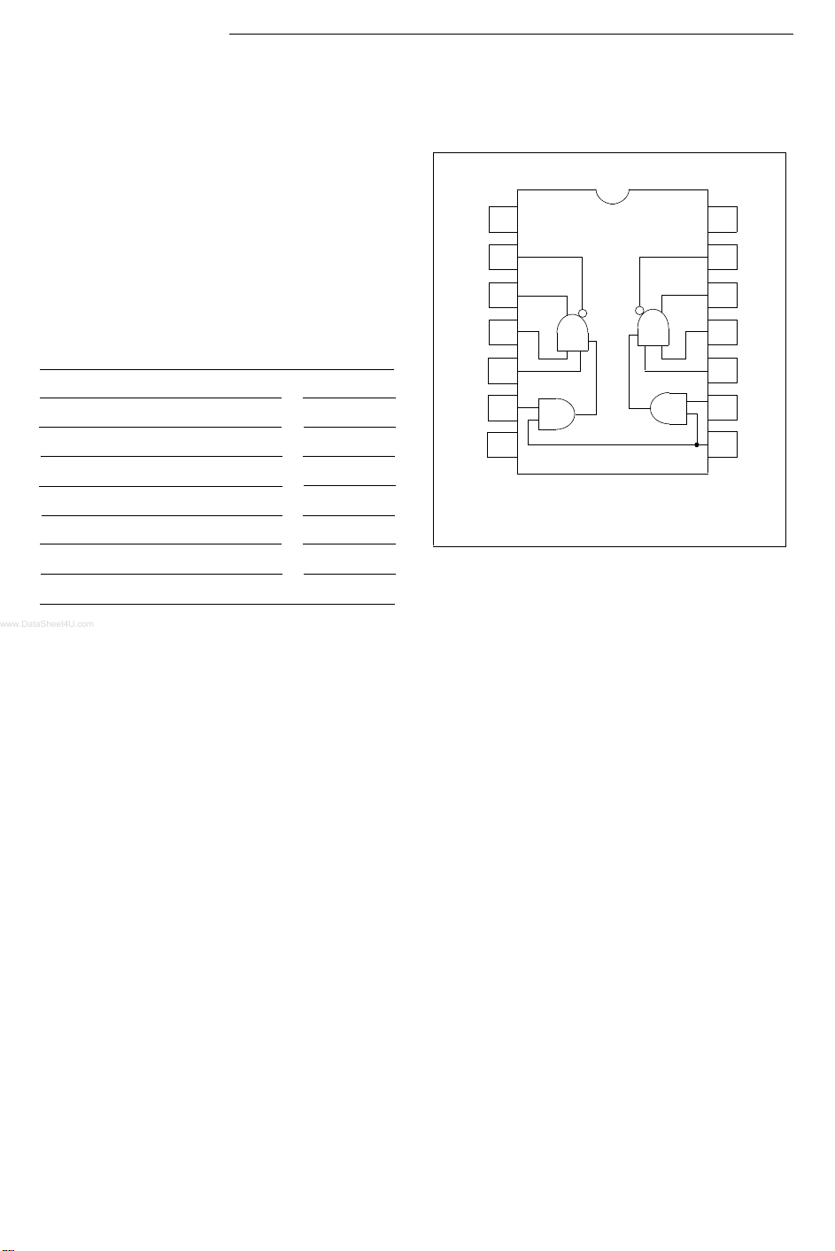
Dual Differential Line Drivers With 3 State Outputs
The HD29412 features dual differential line drivers
with three state out puts designed to satisf y the
requirements of EIA–422. Each driver has an
output control is low, the associated outputs are in a
high impedance state. This permits many deviced
to be connected together on the same transmission
line for party line applications.
Function Table
Input
A
HH
H
L
LL
X
X
:
High level
H
:
Low level
L
:
Irrelevant
X
:
High impedance
Z
B
L
H
X
X
C
H
H
H
H
L
X
D
H
H
H
H
X
L
Output
Y
H
L
L
L
Z
Z
Z
L
H
H
H
Z
Z
Pin Arrangement
1
2
1Z
3
1Y
1A
4
5
1B
6
1C
GND
7
(Top View)
14NC
13
12
11
10
VCC
2Z
2Y
2B
2A
2C
9
8
D
Page 2
HD29412
Absolute Maxim um Ra tings
CC
Symbol
V
CC
VIN
PT
Topr
Tstg
Item
Supply Voltage
Input Voltage
Power Dissipation
Operating Temperature
Storage Temperatur e
Notes: 1. The values is define d as of grou nd terminal.
2. The absolute maximum ratings are values which must not individually be exceeded,
and furthermore, no two of whi ch may be realized at the same time.
Recommended Operating Conditions
Item
Supply Voltage
Output Current
Operating Temperature
Symbol
V
IOH
OL
I
Topr
Ratings
*1
7
5.5
1150
0 to + 70
–65 to + 150
Min
Typ Max
4.75 5.00 5.25
0
–40
40
70
HD29412
Unit
V
V
mW
°C
°C
Unit
V
mA
mA
°C
Electrical Characteristics (Ta = 0 to +70°C)
Item Symbol Unit Conditions
Input Voltage
Input Clamp Voltage
Output Voltage
Output Clamp Voltage
V
IH
VIL
VIK
OH
V
VOL
VOK
V
CC = 4.75 V, II = –12 mA
CC = 4.75 V, VIL = 0.8 V
V
IH = 2 V, IOH = –40 mA
V
CC = 4.75 V, VIL = 0.8 V
V
IH = 2 V,IOL = 40 mA
V
VCC = 5.25 V, IO = –40 mA
Min
2
2.5
Typ
*1
Max
V
0.8
–1.5
V
V
0.5
–1.5
V
2
Page 3

HD29412
Item Symbol Conditions Min
Differential Output Voltage
Change In Magunitude Of
Differential Output
Voltage
*1
VOD1
VOD2
VOD
CC = 5.25 V, IO = 0 mA
V
CC = 4.75 V
V
V
CC = 4.75 V
L = 100 Ω
R
2
HD29412
*1
Max
Typ Unit
OD2
2 V
0.4
V
V
Common Mode Output
Voltage
*3
Magunitude of Common
Mode Output Voltage
*2
Output Current With
Power Off
Off State (High
Impedance)
Output Current
Input Current
(A, B, C Input)
Input Current
(D Input)
Short Circuit Output I
*4
Supply Current
(All Input GND)
VOC
IO
IOZ
V
CC = 5.25 V
V
CC = 4.75 V
CC = 4.75 V or 5.25 V
V
VOC
VCC = 0 100
CC = 5.25 V
V
Output Control
= 0.8 V
I
I
IIH
IIL
II
IIH
IIL
OS VCC = 5.25 V
ICC
CC = 5.25 V, VI = 5.5 V
V
CC = 5.25 V, VI = 2.4 V
V
V
CC = 5.25 V, VI = 0.4 V
VCC = 5.25 V, VI = 5.5 V
V
CC = 5.25 V, VI = 2.4 V
V
CC = 5.25 V, VI = 0.4 V
VCC = 5.25 V, Ta = 25°C
VO = 6 V
V
O = –0.25 V
V
O = –0.25 V to 6 V
Ta = 25°C, V
Ta = 70°C
O = 0 to VCC
VO = 0 V
O = 0.4 V
V
V
O = 2.4 V
V
O = VCC
31
3
3
0.4
–100
±100
±10
–20
±20
±20
20
1
40
–1.6
2
80
–1.8
–150–40
V
V
µA
µA
mA
µA
mA
mA
µA
mA
mA
mA65
Notes: 1. All typical values are at VCC = 5.0 V, Ta = 25°C
VOCVOD
2.
3.
4.
and
respectively. Voltage generated when input level is changed from high to low.
Voc is the average of two output voltages referenced to GND, and is indentical to
output offset volta ge (V
Not more than one output should be shorted at a time and duration of the short
denote the change of VOD and VOC in absolute values,
OS) in EIA standard RS–422.
circuit sho uld not exceed one second.
3
Page 4

HD29412
50 Ω
VOD2
50 Ω
Switching Characteristics (VCC = 5 V, Ta = 25°C)
VOC
HD29412
Item
Propagation Delay
Time
Transition Time
Output Enable
Time
Out p ut Disa b le
Time
Over Shoot
Coefficient
Symbol Unit Conditions Min Typ Max
t
PLH
tPHL
tPLH
tPHL
t
TLH
tTHL
ZH
t
tZL
tHZ
tLZ
Test Circuit
1 Connection A
1 Connection B
1 Connection A
2
3
2
3
2, Connection C
CL = 30 pF, RL = 100 Ω
L = 15 pF
C
C
L = 30 pF, RL = 100 Ω
C
L = 30 pF, RL = 180 Ω
L = 30 pF, RL = 250 Ω
C
C
L = 30 pF, RL = 180 Ω
C
L = 30 pF, RL = 250 Ω
L = 100 Ω
R
16
11
13
9
4
4
7
14
10
17
25
20
20
15
20
20
20
40
30
35
10
ns
ns
ns
ns
%
4
Page 5

HD29412
Switching Time Test Circuit
1.
HD29412
5 V
Pulse
Generator
Connection A
Connection B
1 KΩ
Input
Y
Z
Y
Z
50 Ω
CL = 15 pF
CL =
30 pF
Y
Z
R
L = 100 Ω
CL = 15 pF
Output
25 ns
5 ns
Input
10 % 10 %
Y
Z
Over Shoot
100 %
90 %90 %
1.5 V
tPLH
1.5 V
10 %
tPHL tPLH
1.5 V
90 %90 %
tTLH
1.5 V 1.5 V
10 %10 %
tTHL tTLH
≈
5 ns
tPHL
tTHL
1.5 V
10 %
90 %90 %
3 V
0 V
VOH
VOL
VOH
VOL
Connection C
Y
Z
0 %
Over Shoot
RL = 100 Ω
5
Page 6

HD29412
2. tZH, tHZ
HD29412
Input
5ns 10ns
Pulse
Generator
1 K
5 V
3. tZL, tLZ
Pulse
Generator
1 KΩ
50 Ω
Input
5 V
CL =
30 pF
CL =
30 pF
CL =
30 pF
C
L =
30 pF
5 V
RL =
250 Ω
Output
Output
RL =
180 Ω
Input
1.5 V
90 %90 %
1.5 V
10 % 10 %
100ns
t
ZH
Output
1.5 V
5ns 10ns
Input
10 % 10 %
Output
1.5 V
ZL
t
90 %90 %
1.5 V
100ns
1.5 V
tHZ
tLZ
0.5 V
0.5 V
3 V
0 V
V
OH
Voff
≈ 0 V
3 V
0 V
5 V
V
OL
Notes: 1. The pulse generator has the following characteristics : PRR = 500 KH
2. C
L includes probe and jig capacitance.
6
Z, ZOUT = 50 Ω.
 Loading...