

Page 1
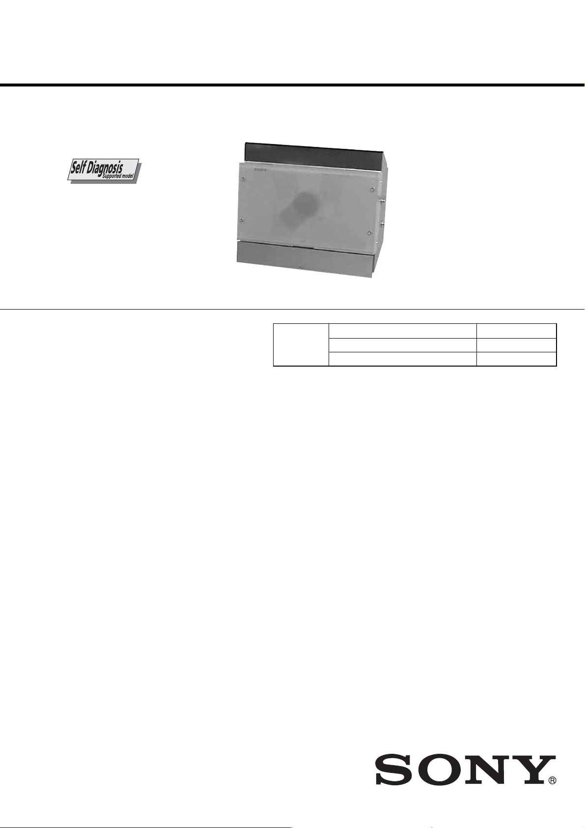
HCD-L7HD
Amplifier section
For the U.S. model
AUDIO POWER SPECIFICATIONS
POWER OUTPUT AND TOTAL
HARMONIC DISTORTION:
With 4-ohm loads, both channels driven, from
120 - 10,000 Hz; rated 25 watts per channel
minimum RMS power, with no more than 10%
total harmonic distortion from 250 milliwatts to
rated output.
North American model:
Continuous RMS power output (reference):
25 + 25 W
(4 ohms at 1 kHz, 10%
THD)
European model:
DIN power output (rated): 20 + 20 W
(4 ohms at 1 kHz, DIN)
Continuous RMS power output (reference):
25 + 25 W
(4 ohms at 1 kHz, 10%
THD)
Music power output (reference):
25 + 25 W
Other models:
The following measured at 220 V AC, 60 Hz
DIN power output (rated): 20 + 20 W
(4 ohms at 1 kHz, DIN,
110 V - 240 V AC)
Continuous RMS power output (reference):
25 + 25 W
(4 ohms at 1 kHz, 10%
THD, 110 V - 240 V AC)
Inputs
MD/TAPE IN (stereo minijack):
Sensitivity 450 mV (MD)/
250 mV (Tape),
impedance 47 kilohms
DIGITAL OPTICAL IN (Supported sampling
frequencies: 32 kHz, 44.1 kHz and 48 kHz)
Outputs
MD/TAPE OUT (stereo minijack):
Sensitivity 250 mV,
impedance 1 kilohmes
PHONES (stereo minijack):
Accepts headphones with
an impedance of 8 ohms
or more
DIGITAL CD OPTICAL OUT (Supported sampling
frequency: 44.1 kHz)
CD player section
System Compact disc and digital
audio system
Laser Semiconductor laser
(λ = 795 nm)
Emission
duration: continuous
Frequency response 2 Hz – 20 kHz
HD recorder section
Capacity 20 GB
Recording system ATRAC 3
Transfer rate 132 kbps
Maximum recording time About 300 h
Maximum number of albums
Library area: 250
Flexible area: 250
Maximum number of tracks
20,000
Maximum number of tracks per album
400
Maximum CD-HD ripping speed
Max. ×2
Tuner section
FM stereo, FM/AM superheterodyne tuner
FM tuner section
Tuning range
North American model: 87.5 - 108.0 MHz
(100-kHz step)
Other models: 87.5 - 108.0 MHz
(50-kHz step)
Antenna FM wire antenna
Antenna terminals 75 ohm unbalanced
Intermediate frequency 10.7 MHz
AM tuner section
Tuning range
North American model: 530 - 1,710 kHz
(with the tuning interval
set at 10 kHz)
531 - 1,710 kHz
(with the tuning interval
set at 9 kHz)
European model: 531 - 1,602 kHz
(with the tuning interval
set at 9 kHz)
Other models: 530 - 1,710 kHz
(with the tuning interval
set at 10 kHz)
531 - 1,602 kHz
(with the tuning interval
set at 9 kHz)
Antenna AM loop antenna, external
antenna terminal
Intermediate frequency 450 kHz
SERVICE MANUAL
Ver 1.2 2003. 12
This set is the tuner, CD, HD and amplifier
section in CMT-L7HD.
CD
SECTION
SPECIFICATIONS
US Model
Canadian Model
AEP Model
UK Model
Model Name Using Similar Mechanism NEW
CD Mechanism Type CDM71B
Base Unit Type BU-31BD63
9-874-073-03
2003L16-1
© 2003.12
Sony Corporation
Home Audio Company
Published by Sony Engineering Corporation
MICRO Hi-Fi COMPONENT SYSTEM
— Continued on next page —
Page 2

HCD-L7HD
General
Power requirements
North American model: 120 V AC, 60 Hz
European model: 230 V AC, 50/60 Hz
Other models: 110 - 240 V AC ,
Power consumption
European model: See the nameplate
Other models: See the nameplate
Dimensions (w/h/d) Approx. 293 × 246 ×
Mass Approx. 4.3 kg
Design and specifications are subject to change
without notice.
50/60 Hz
0.2 W (at the Power
Saving Mode)
131 mm incl. projecting
parts and controls
Self-diagnosis display
Messages
One of the following messages may appear or
flash in the display during operations.
CD
Complete!
CD editing (Disc Memo) finished normally.
File Full
There are already 100 disc titles stored in the
system.
Initialize
The system is being initialized. You cannot load a
CD during this time. Wait until “Initialize”
disappears from the display.
No Disc
There is no disc in the CD player.
—OVER—
You have reached the end of the CD while
pressing and holding down M during playing
pause.
Push STOP!
You pressed PLAY MODE on the remote during
playback.
You pressed STORAGE MODE during playback.
You pressed STORAGE MODE during manual
recording of a CD.
Step Full!
You tried to program 26 tracks (steps) or more.
HD
Already Done
You tried to perform High-Speed Synchro Storage
for a CD that has already been completely
recorded.
Auto Cut
The system is pausing the recording because
silence continued for 30 seconds or more during
digital recording.
Blank Disc
There is no track on the HD.
2
Page 3

HCD-L7HD
Cannot Copy
You tried to play a CD with a format that the
system does not support, such as a CD-ROM. The
sound source is a copy of commercially available
music software.
Cannot Edit
You tried to edit in Shuffle Play, or you tried to
register a track to a playlist that already contains
400 tracks.
Cannot Play
The system cannot play the track because of
damage to the audio data.
Cannot Rec
You tried to record to the HD with HD selected as
the sound source.
You tried to perform manual recording from the
CD with “AUTO” selected as the storage mode.
You pressed REC with “AUTO” selected as the
storage mode.
You tried to record a CD to the HD without
loading the CD.
Cannot STORAGE
You tried to record to the HD with less than 131
recordable tracks remaining on the HD.
You tried to record to the HD with less than 240
minutes of recordable time remaining on the HD.
You tried to perform High-Speed Synchro Storage
with no blank album in the Library area.
Check OPT-IN
A moment’s lighting is due to the signals of the
digital program being recorded. This does not
affect the recorded material.
While recording from a digital component
connected through the DIGITAL OPTICAL IN
jack, the digital connecting cable was unplugged or
the digital component turned off.
Complete!
The editing operation of the HD is completed.
The system is copying a title or artist name.
Copying
The system is copying the text data.
Drive Error
Consult your Sony dealer or local authorized Sony
service facility.
Drive Full!
Recording tracks is not possible because there is
not enough recordable space on the HD or the
maximum number of recordable tracks has been
reached.
Erasing
The system is erasing data from the HD. Do not
disconnect the power cord.
Format Error
Consult your Sony dealer or local authorized Sony
service facility.
Impossible
You tried to make an impossible editing or
recording operation.
Library Making
The system is recording data to the HD.
Name Full!
The naming capacity of the HD has reached its
limit (about 127 characters).
No Name
The album or track has not been labelled.
No Signal
The system has detected a silent portion during
recording.
Not Found
No matches were found for Keyword Search.
Please Wait
You tried to perform High-Speed Synchro Storage
while the system was collating data between the
CD and the HD.
You tried to perform High-Speed Synchro Storage
while the system was preparing for Auto Storage
and High-Speed Synchro Storage.
Push STOP!
You pressed PLAY MODE on the remote during
playback.
You pressed SEARCH on the remote during
playback.
Rec Error
Proper recording is not possible.
– Rehearsal –
The HD is playing the specified dividing point for
confirmation during the Divide function.
The HD is playing the specified Highlight position
for confirmation during the Highlight Play
function.
REMOTE
The system is being connected to your computer.*
Retry
The system is retrying reading data from the CD
during High-Speed Synchro Storage.
Smart Space
The signal was input again after silence continued
for 3 or more but less than 30 seconds during
digital recording.
STORAGE NOW
You tried to turn off the system while the system
was storing data to the HD.
TOC Reading
The system is reading data from the HD.
Track End
You have reached the end of the track while
adjusting the dividing point during the Divide
function.
Track Full!
Recording tracks is not possible because there are
400 tracks in the album. Select another album for
recording.
Timer
OFF TIME NG!
The stopping time is the same as the starting time
in the Daily Timer operation.
OVERLAP!
The Daily Timer or timer-recording setting that
you attempted to make partially or wholly
coincides with another setting.
* If “REMOTE” appears under other circumstances,
turn off the system, then turn on it again.
3
Page 4

HCD-L7HD
TABLE OF CONTENTS
1. SERVICING NOTES
2. GENERAL ·········································································· 8
3. DISASSEMBLY ······························································ 10
3-1. Bottom Plate,Case ·······················································11
3-2. Front Panel Section ····················································· 11
3-3. POWER Board, AM/FM Tuner ··································· 12
3-4. HDD Board, HDD SUB Board ··································· 12
3-5. MAIN Board ······························································· 13
3-6. Cover (HDD-Top), Cover (HDD-Bottom) ·················· 13
3-7. AMP Board, REG Board ············································· 14
3-8. Switching Regulator ···················································· 14
3-9. Indicator (BS), LED Board (R) ···································15
3-10.LED Board (L) ···························································· 15
3-11.FL Board ·····································································16
3-12.TOUCH SW Board, SWITCH Board ························· 16
3-13.CD Board·····································································17
3-14.BD Board·····································································17
3-15.Base Unit (BU-31BD63) ············································· 18
3-16.BU-31 Assy, Sled Motor Assy (M102) ······················· 18
3-17.CD Mechanism (CDM71B) ········································ 19
3-18.L.MOTOR Board ························································· 19
3-19.C.MOTOR Board, L.SENSOR Board ························· 20
3-20.ENCODER Board, D.SENSOR Board ······················· 21
3-21.Pulley (RTR) Assy, Pulley (RTL) Assy,
Belt (CDM71), Belt (Roller) (L) ································· 22
3-22.Pulley (SPT) Assy, Gear (RT) Assy, Gear(KT),
Belt (CDM71) ····························································· 24
4. TEST MODE ···································································· 26
······················································· 5
6. DIAGRAMS······································································31
6-1. Block Diagrams ··························································· 31
6-2. Circuit Boards Location ·············································· 34
6-3. Printed Wiring Board – BD Section (Side A) – ··········· 35
6-4. Printed Wiring Board – BD Section (Side B) –···········36
6-5. Schematic Diagram – BD Section – ···························· 37
6-6. Printed Wiring Board – MOTOR Section – ················38
6-7. Schematic Diagram – MOTOR Section – ··················· 39
6-8. Printed Wiring Board – HDD1 Section (Side A) – ····· 40
6-9. Printed Wiring Board – HDD1 Section (Side B) – ·····41
6-10.Schematic Diagram – HDD1 Section (1/2) –·············· 42
6-11.Schematic Diagram – HDD1 Section (2/2) –·············· 43
6-12.Printed Wiring Board – HDD2 Section –···················· 44
6-13.Schematic Diagram – HDD2 Section (1/2) –·············· 45
6-14.Schematic Diagram – HDD2 Section (2/2) –·············· 46
6-15.Printed Wiring Board – MAIN Section (Side A) – ····· 47
6-16.Printed Wiring Board – MAIN Section (Side B) – ·····48
6-17.Schematic Diagram – MAIN Section (1/2) –·············· 49
6-18.Schematic Diagram – MAIN Section (2/2) –·············· 50
6-19.Printed Wiring Board – CD Section – ························· 51
6-20.Schematic Diagram – CD Section –····························52
6-21.Printed Wiring Board – AMP Section (Side A) –········ 53
6-22.Printed Wiring Board – AMP Section (Side B) – ········ 54
6-23.Schematic Diagram – AMP Section – ························· 55
6-24.Printed Wiring Board – DISPLAY Section – ·············· 56
6-25.Schematic Diagram – DISPLAY Section – ················· 57
6-26.Printed Wiring Board – CONTROL Section – ············ 58
6-27.Schematic Diagram – CONTROL Section –···············59
6-28.Printed Wiring Board – POWER Section –·················60
6-29.Schematic Diagram – POWER Section – ··················· 61
6-30.IC Pin Function Descriptions ······································ 63
5. ELECTRICAL ADJUSTMENTS ·······························30
7. EXPLODED VIEWS ······················································ 72
7-1. Case Section ································································72
7-2. Chassis Section ···························································· 73
7-3. Frot Panel Section ······················································· 74
7-4. Mechanism Section(CDM71B)-1································ 75
7-5. Mechanism Section(CDM71B)-2································ 76
7-6. Base Unit (BU-31BD63) ············································· 77
8. ELECTRICAL PARTS LIST ······································· 78
4
Page 5

SECTION 1
SERVICING NOTES
HCD-L7HD
NOTES ON HANDLING THE OPTICAL PICK-UP
BLOCK OR BASE UNIT
The laser diode in the optical pick-up block may suffer electrostatic
break-down because of the potential difference generated by the
charged electrostatic load, etc. on clothing and the human body.
During repair, pay attention to electrostatic break-down and also
use the procedure in the printed matter which is included in the
repair parts.
The flexible board is easily damaged and should be handled with
care.
NOTES ON LASER DIODE EMISSION CHECK
The laser beam on this model is concentrated so as to be focused on
the disc reflective surface by the objective lens in the optical pickup block. Therefore, when checking the laser diode emission,
observe from more than 30 cm away from the objective lens.
Laser component in this product is capable
of emitting radiation exceeding the limit for
Class 1.
This appliance is classified as a CLASS 1 LASER product. The
CLASS 1 LASER PRODUCT MARKING is located on the rear
exterior.
SAFETY CHECK-OUT
After correcting the original service problem, perform the
following safety checks before releasing the set to the customer:
Check the antenna terminals, metal trim, “metallized” knobs, screws,
and all other exposed metal parts for A C leakage. Check leakage as
described below.
LEAKAGE
The A C leakage from any exposed metal par t to earth ground and
from all exposed metal parts to any exposed metal part having a
return to chassis, must not exceed 0.5 mA (500 microamperes).
Leakage current can be measured by any one of three methods.
1. A commercial leakage tester, such as the Simpson 229 or RCA
WT -540A. Follo w the manufacturers’ instructions to use these
instruments.
2. A battery-operated AC milliammeter. The Data Precision 245
digital multimeter is suitable for this job.
3. Measuring the voltage drop across a resistor by means of a
VOM or battery-operated AC voltmeter . The “limit” indication
is 0.75 V, so analog meters must have an accurate lo w-v oltage
scale. The Simpson 250 and Sanwa SH-63Trd are e xamples of
a passive VOM that is suitable. Nearly all battery operated
digital multimeters that have a 2V AC range are suitable. (See
Fig. A)
To Exposed Metal
Parts on Set
This caution
label is
located inside
the unit.
CAUTION
Use of controls or adjustments or performance of procedures
other than those specified herein may result in hazardous radiation
exposure.
SAFETY-RELATED COMPONENT WARNING!!
COMPONENTS IDENTIFIED BY MARK 0 OR DOTTED LINE WITH
MARK 0 ON THE SCHEMATIC DIAGRAMS AND IN THE PARTS
LIST ARE CRITICAL TO SAFE OPERATION. REPLACE THESE
COMPONENTS WITH SONY PARTS WHOSE PART NUMBERS
APPEAR AS SHOWN IN THIS MANUAL OR IN SUPPLEMENTS
PUBLISHED BY SONY .
AC
0.15 µF
Fig. A. Using an A C v oltmeter to check A C leakage.
1.5 kΩ
Earth Ground
Voltmeter
(0.75 V)
Notes on chip component replacement
•Never reuse a disconnected chip component.
• Notice that the minus side of a tantalum capacitor may be
damaged by heat.
Flexible Circuit Board Repairing
•Keep the temperature of soldering iron around 270˚C
during repairing.
• Do not touch the soldering iron on the same conductor of the
circuit board (within 3 times).
• Be careful not to apply force on the conductor when soldering
or unsoldering.
ATTENTION AU COMPOSANT AYANT RAPPORT
LES COMPOSANTS IDENTIFÉS P AR UNE MARQUE 0 SUR LES
DIAGRAMMES SCHÉMA TIQUES ET LA LISTE DES PIÈCES SONT
CRITIQUES POUR LA SÉCURITÉ DE FONCTIONNEMENT. NE
REMPLACER CES COMPOSANTS QUE PAR DES PIÈSES SONY
DONT LES NUMÉROS SONT DONNÉS DANS CE MANUEL OU
DANS LES SUPPÉMENTS PUBLIÉS PAR SONY.
À LA SÉCURITÉ!
5
Page 6

HCD-L7HD
NOTES ON HARD DISC
The hard disc has a high storage density and reads or writes data in
a short time with compared to the floppy disk. On the other hand, it
may be easily damaged by mechanical vibration, shock or dust.
Keep the hard disc away from magnets.
Although the hard disc has safety devices to prevent losing data due
to mechanical vibration, shock or dust, you should be careful when
handling the recorder. Avoid damaging your data:
• Do not cause a shock or strong vibration to the recorder.
• Do not place the recorder in a location subject to mechanical
vibration or in unstable location.
• Do not move the recorder while the power is on.
• Do not turn off the recorder while the HDD indicator lights up
blue.
• Do not use the recorder in a place subject to extreme changes in
temperature (temperature gradient less than 18 °F (10 °C)/ hour).
•Keep any magnetic objects, including a TV set, speaker , magnet,
and magnetic bracelet, away from the recorder.
If the hard disc is damaged, data cannot be restored or recovered.
NOTES ON DIGITAL AMPLIFIER
Cause of the Digital Amplif ier, do not connect the speaker ter minals
to the chasis, or connect the terminals of the right speakers with
those of the left speaker. (None of the speaker terminals is the
negative(–) terminal of the speak er. So,do not connect the earth lead
of this unit to the speaker terminals.)
Unleaded solder
Boards requiring use of unleaded solder are printed with the leadfree mark (LF) indicating the solder contains no lead.
(Caution: Some printed circuit boards may not come printed with
the lead free mark due to their particular size.)
: LEAD FREE MARK
Unleaded solder has the following characteristics.
• Unleaded solder melts at a temperature about 40°C higher than
ordinary solder.
Ordinary soldering irons can be used but the iron tip has to be
applied to the solder joint for a slightly longer time.
Soldering irons using a temperature regulator should be set to
about 350°C.
Caution: The printed pattern (copper foil) may peel away if the
heated tip is applied for too long, so be careful!
• Strong viscosity
Unleaded solder is more viscous (sticky , less prone to flo w) than
ordinary solder so use caution not to let solder bridges occur such
as on IC pins, etc.
• Usable with ordinary solder
It is best to use only unleaded solder but unleaded solder may
also be added to ordinary solder.
6
Page 7

• Service Position -1
)
d
HCD-L7HD
BD board
FL board
JIG
(J-2501-077-A)(13P)
JIG
(J-2501-167-A)(17P)
FM/AM tuner
JIG
(J-2501-076-A)(11P
chassis
• Service Position -2
(Checking For Hard Disc Section)
BD board
JIG
(J-2501-077-A)(13P)
JIG
(J-2501-167-A)(17P)
hard disk
JIG
(J-2501-202-A)(11P)
HDD SUB boar
HDD IF board
FM/AM tuner
JIG
(J-2501-076-A)(11P)
chassis
7
Page 8

HCD-L7HD
Main unit
SECTION 2
GENERAL
This section is extracted
from instruction manual.
ALPHABETICAL ORDER
A – H
ALBUM dial qf (18, 19, 21, 26)
CD cover 2 (14, 15)
CD u qa (14 - 16, 25)
CD x qs (15, 16, 24, 25)
DISPLAY 8 (39, 44, 45)
Display window 1 (44, 45)
FUNCTION qh (14 - 22, 25 - 28,
30, 32 - 35, 57)
HD u 9 (18, 20 - 22, 25, 26)
HD x q; (18, 25, 26, 30)
HIGH SPEED SYNC ql (25)
P – Z
PHONES jack 7
REC w; (26, 28)
Remote sensor 6
STORAGE MODE qk (14, 25,
26)
TUNER/BAND qd (37, 38)
TUNING +/– qj (37, 38)
VOL +/– qg (41)
1
BUTTON DESCRIPTIONS
@/1 (power) 4 (11, 41, 42)
./> qj (15, 16, 18)
m/M qj (15, 18)
Z 3 (14, 15)
V OPEN 5
To open the front cover, push
down on V OPEN.
2
3
6
789q;
qlqk
54
qaqsqd
qgqhqjw;
qf
8
Page 9

Remote control
HCD-L7HD
ALPHABETICAL ORDER
ALBUM eh (19)
ALBUM FAVORITES 7 (22)
ALBUM MEMORY 8 (22)
ALBUM +/– 6 (18, 19, 21, 26)
CAPS rd (16, 31)
CD N wa (14 - 16, 25)
CD X qa (15)
CD x q; (15, 16, 24, 25)
CLEAR es (15 - 17, 29, 31, 39)
CLOCK/TIMER SELECT eg
(41 - 43)
CLOCK/TIMER SET ef (13, 41,
42)
CURSOR T/t el (13, 17, 20,
21, 31, 35, 42)
DIMMER 5 (44)
DISPLAY wk (39, 44, 45)
DSG qk (40)
ENTER/YES e; (13, 15 - 17,
19 - 21, 27 - 37, 39, 41 - 43, 57)
FM MODE qg (38)
FUNCTION ws (14 - 22, 25 - 28,
30, 32 - 35, 57)
HD N wd (18, 20 - 22, 25, 26)
HD X wf (18, 25, 26)
HD x 9 (18, 25, 26, 30)
HIGHLIGHT wg (21)
HISTORY +/– wh (22)
MENU/NO ek (17, 20, 27 - 39,
57)
MENU +/– r; (13, 17, 20, 21,
27 - 36, 41 - 43)
NAME rs (16, 39)
Numeric buttons for selecting an
album or track ej (15, 19, 38)
PLAYLIST ed (19, 20)
PLAY MODE qh (14 - 18, 21)
PRESET EQ qj (40)
REPEAT qg (15, 18)
SCROLL 4 (17, 45)
SEARCH ea (20)
SLEEP 2 (40)
SML ra (16, 31)
Text input buttons wl (16, 31)
TIME wj (16, 44, 45)
TUNER BAND w; (37, 38)
TUNING MODE qh (37, 38)
TUNING +/– qs (37, 38)
VOL +/– qf (41)
BUTTON DESCRIPTIONS
@/1 (power) 3 (11, 41, 42)
./> ql (15, 16, 18)
m/M qd (15, 18)
Z 1 (14, 15)
12 3
wk
wj
wh
wg
wf
wd
ws
wa
w;
ql
qk
qj
qh
qg
4
5
6
7
8
9
q;
qa
qs
qd
qf
rd
rs
ra
r;
el
ek
wl
e;
ea
es
ed
ej ehegef
Setting the clock
1 Turn on the system.
2 Press CLOCK/TIMER SET on the
remote.
3 Press MENU + or – on the remote
repeatedly to set the day, and then
press ENTER/YES or CURSORt on
the remote.
The hour indication flashes.
4 Press MENU + or – on the remote
repeatedly to set the hour, and then
press ENTER/YES or CURSORt on
the remote.
The minute indication flashes.
5 Press MENU + or – on the remote
repeatedly to set the minute, and then
press ENTER/YES on the remote.
If you make a mistake
Press TCURSOR or CURSORt on the
remote repeatedly until the indication you want
to change (day, hour, minute) flashes, and then
change the setting.
To adjust the clock
1
Press CLOCK/TIMER SET on the remote.
2
Press MENU + or – on the remote repeatedly
until “CLOCK SET?” appears in the display,
and then press ENTER/YES on the remote.
3
Do the same procedures as steps 3 to 5
above.
9
Page 10

HCD-L7HD
SECTION 3
DISASSEMBLY
Note : This set can be disassembled in the order shown below.
SET (HCD-L7HD)
POWER BOARD,
AM/FM TUNER
HDD BOARD,
HDD SUB BOARD
AMP BOARD,
REG BOARD
INDICATOR (BS),
LED BOARD (R)
LED BOARD (L)
BOTTOM PLATE,CASE
MAIN BOARD
COVER (HDD-TOP),
COVER (HDD-BOTTOM)
SWITCHING REGULATOR
FRONT PANEL SECTION
FL
BOARD
TOUCH SW BOARD,
SWITCH BOARD
CD MECHANISM
(CDM71B)
CD
BOARD
BD
BOARD
BASE UNIT
(BU-31BD63)
C.MOTOR BOARD,
L.SENSOR BOARD
L.MOTOR BOARD
HOLDER ASSY ,
SLED MOTOR ASSY (M102)
ENCODER BOARD,
D.SENSOR BOARD
10
PULLEY (RTR) ASSY,PULLEY (RTL) ASSY,
BELT (CDM71), BELT (ROLLER) (L)
PULLEY (SPT) ASSY,GEAR (RT)ASSY,
GEAR (KT), BELT (CDM71)
Page 11

Note : Follow the disassembly procedure in the numerical order given.
e
3-1. Bottom Plate,Case
qg
case
6
t
wo screws (SS)
7
s
qa
t
wo screws
(+PTT 3
3
earth plate
× 6
crew (+PTT 3
)
× 6
)
qd
qf
c
onnector
(CN801)
three
claws
qs
5
f
our screws (SS)
8
t
HCD-L7HD
wo screws (SS)
1
six screws (+BVTP 3
3-2. Front Panel Section
qa
front panel section
× 8
9
s
crew (+PTT 3
q;
t
wo screws (+PTT 3
4
b
ottom plate
2
three screws (+BVTP 2.6
)
q;
c
hassis section
7
1
two
earth plates
× 6
)
×
8)
6
two screws (+BVTP 2.6
flat type wire (17 core)
5
two
screws (+BVTP 2.6
×
× 6
)
8)
×
8)
9
f
lat type wire (13 core)
8
c
onnector
(CN1321)
4
c
onnector (CN1201)
2
3
ground wir
screw (+BVTP 3
×
6)
11
Page 12

HCD-L7HD
)
)
3-3. POWER Board, AM/FM Tuner
3
4
connector (CN851)
q;
AM/FM t
uner
9
flat type wire
(11core or 15core)
connector (CN800)
1
two
screws
(+BVTP 3
7
POWER board
5
connector (CN852)
2
connector (CN500)
6
connector (CN803
×
8)
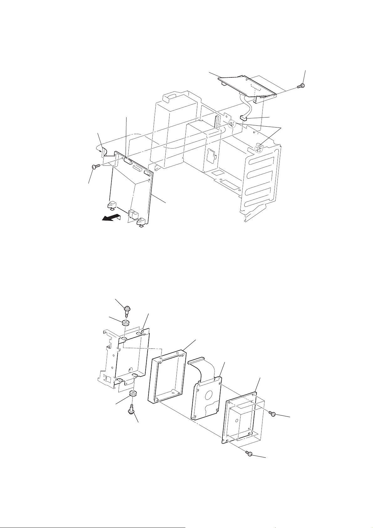
3-4. HDD Board, HDD SUB Board
6
4
two
screws
(+BVTP 3
×
8)
HDD IF board
3
connector
(CN507,508,503)
7
(+BVTT 3
three
screws
×
6)
5
(CN1002)
harness
8
two
screws
(+BVTP 3
×
8)
2
four
screws
(+BVTP 3
×
8
12
8
HDD SUB board
1
screw
(+BVTP 3
×
8)
Page 13
3-5. MAIN Board
)
)
5
flat type wire (23core)
three
6
(+BVTP 3
screws
3
connector (CN500)
×
8)
4
POWER
board
2
two
screws (+BVTP 3
1
connector (CN504)
8
two
HCD-L7HD
×
claws
8
9
7
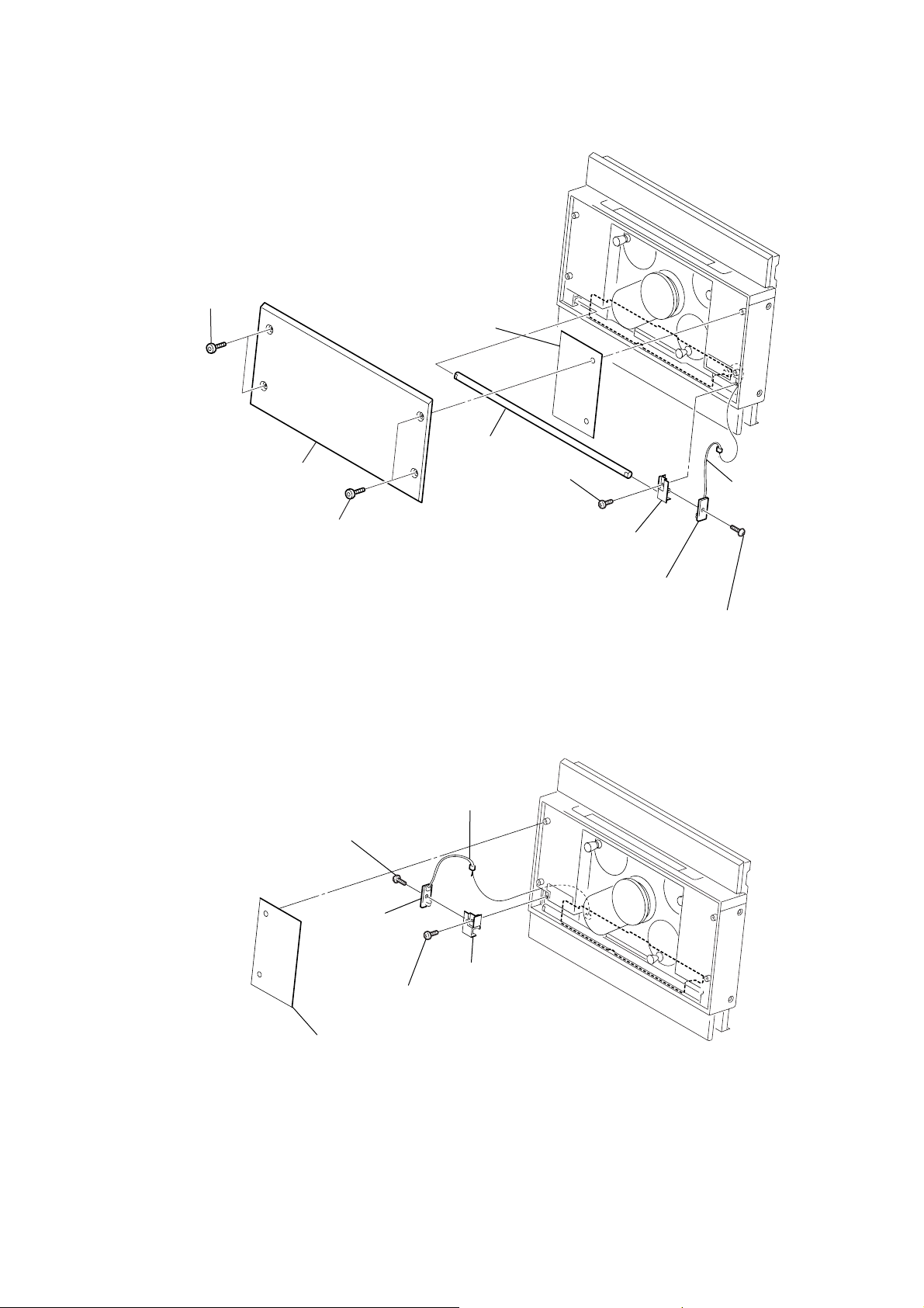
3-6. Cover (HDD-Top), Cover (HDD-Bottom)
1
two
screws
(+BVTPWH M3)
5
shield case (HDD)
2
two insulators
MAIN board
7
cover (HDD-top)
9
HDD
q;
cover (HDD-bottom)
4
two insulators
3
two
screws
(+BVTPWH M3)
6
four
(+BVTP 3
8
four
(+BVTT 3
screws
×
8)
screws
×
6
13
Page 14

HCD-L7HD
)
3-7. AMP Board, REG Board
9
connector (CN300)
q;
three
screws
× 6
screws
×
)
8)
(+BVTP 3
6
three
(+BVTP 3
qa
two
1
connector (CN851)
hooks
qs
3
flat type wire (23core)
2
connector (CN800)
5
screw
(+BVTP 3
×
8
7
8
shield case (SM-top)
3-8. Switching Regulator
6
(+BVTP 3
ground wire
qg
screw
AMP board
1
(+BVTP 3
×
8)
qf
(SM-bottom)
four
screws
4
shield case
×
6)
connector
qj
REG
board
qd
connector (CN804)
qh
screw
(+BVTP 3
3
4
two
screws
(+BVTP 3
×
8)
two
hooks
×
8)
14
5
screw
(+BVTP 3
q;
switching
7
(+BVTP 3
×
8)
regurator
two
screws
8
×
8)
nylon rivet
2
9
sheet (power box)
Page 15
3-9. Indicator (BS), LED Board (R)
r
2
two screws
(panel)
3
ornamental plate (CD)
1
two screws
(panel)
4
sheet (CD2)
8
indicator (BS)
6
s
crew (+BTP 2.6
×
6)
7
holder (LED-R)
HCD-L7HD
5
connecto
(CN1303)
3-10. LED Board (L)
5
screw (+BVTP 2.6
×
8)
6
LED board (L)
1
connector (CN1302)
4
3
screw (+BTP 2.6
holder (LED-L)
×
6)
q;
LED board (R)
9
screw (+BVTP 2.6
×
8)
2
sheet (CD2)
15
Page 16

HCD-L7HD
)
d
3-11. FL Board
2
FL board
1
two
screws (+BVTP 2.6
×
8
3-12. TOUCH SW Board, SWITCH Board
5
knob jog assy
2
TOUCH SW board
1
two
(+BVTP 2.6
screws
×
8)
3
c
onnector (CN1302)
7
SWITCH boar
16
4
c
onnector (CN1303)
6
f
ive screws
(+BVTP 2.6
×
8)
Page 17

3-13. CD Board
)
)
4
c
onnector
(CN751)
1
f
lat type wire (19 core)
7
bracket (CD-MT)
6
two screws (+BVTP 3
5
CD board
×
8)
2
three screws
(+BVTP 2.6
HCD-L7HD
×
8
3-14. BD Board
3
c
onnector
(CN752)
1
Remove solder (two portions ).
(BLK)
6
BD board
5
h
ook
4
flxible
(RED)
board
2
Remove solder (two portions ).
3
screw
(+BTP 2.6
×
8
17
Page 18

HCD-L7HD
)
3-15. Base Unit (BU-31BD63)
Rotate the SPT pulley assy in the direction of to move the base unit shaft
forward.
1
SPT pulley assy
1
cam (A)
shaft
shaft
4
2
screw
(+PTPWH M2.6)
5
base unit
(BU-31BD63
3
3-16. BU-31 Assy, Sled Motor Assy (M102)
9
two screws
(+PTPWH M2.6)
holder assy
7
coil spring (C) (holder)
5
BD board
q;
qs
screw
(+P 2
h
×
ook
8
screw
(+PTPWH M2.6)
qa
BU-31 assy
4
flxible
board
qd
sled motor assy (M102)
3)
6
coil spring (B) (holder)
1
(two portions ).
(RED)
(BLK)
Remove solder
18
3
screw
(+BTP 2.6
×
2
8)
Remove solder
(two portions ).
Page 19

3-17. CD Mechanism (CDM71B)
1
two
claws
2
cap (chuck) assy
7
blacket
8
CD mechanism (CDM71B)
HCD-L7HD
4
two
screws
(+BVTP 2.6
×
8)
3-18. L.MOTOR Board
6
six
screws (+BTP 2.6
×
3
sheet
5
two
screws
×
× 6
8)
)
(+BVTP 2.6
6)
1
Remove solder (two portions ).
2
two
screws
(+BTP 2.6
3
connector
(CN711)
4
L.MOTOR board
19
Page 20

HCD-L7HD
)
3-19. C.MOTOR Board, L.SENSOR Board
3
connector
(CN711)
5
(CN753)
c
onnector
6
(CN755)
4
c
onnector
(CN754)
c
onnector
8
(+BTP M 2.6
screw
1
Remove solder
(two portions ).
7
C.MOTOR board
×
6)
2
two screws
(+BTP M 2.6
×
6
9
L.SENSOR board (R)
20
Page 21

3-20. ENCODER Board, D.SENSOR Board
7
D.SENSOR board
4
6
(+BTP 2.6
screw (+PWH 2
5
ENCODER
screw
×
HCD-L7HD
Ver 1.2 2003.12
×
6)
2
screw (+BTP 2.6
6)
1
3
cover (encoder)
board
(+BTP 2.6
screw
× 8
×
)
6)
PRECAUTION DURING ENCODER board INSTALLATION
Rotate the pulley (LDG2) until the mark of the cam (A) becomes visible.
Install the ENCODER board in the way that it is sandwiched by
the cut-outs of the ENCODER board.
pulley (LDG2)
ENCODER board
cam (A)
21
Page 22

HCD-L7HD
3-21. Pulley (RTR) Assy, Pulley (RTL) Assy, Belt (CDM71), Belt (Roller) (L)
6
screw
7
D.SENSOR board
(+BTP 2.6
5
ENCODER
(When installing it, see the ENCODER board item.)
×
6)
3
cover (encoder)
4
screw (+PWH 2
board
2
screw (+BTP 2.6
×
6)
× 8
1
screw
(+BTP 2.6
×
)
6)
qf
RTL pulley assy
9
qg
gear (S1)
c
law
qh
belt (CDM71)
q;
8
pulley (RTR) assypulley (RTL) assy
c
law
q;
RTL pulley assy
qd
RTR pulley assy
22
qs
RTR pulley assy
qj
belt (ROLLER) (L)
qa
Page 23

PRECAUTION DURING PULLEY (RTR) ASSY, PULLEY (RTL) ASSY INSTALLATION
pulley (RTR) assy
pulley (RTR) assy
HCD-L7HD
gear (S2)
(9 o'clock position)
pulley (RTL) assy
claw
marks of the gear (S2)
Place the holes of the gear (S2) at the 9 o'clock position and install
the pulley (RTR) assy.
Install it in the way that the gear of the cut-out portion as shown is located in
between the marks of the gear (S2).
pulley (RTR) assy
claw
Then install the pulley (RTL) assy in the way that it can perform
the symmetrical movement with the pulley (RTR) assy.
Then lock both claws.
pulley (RTR) assy
pulley (RTL) assy
Confirm that the pulley (RTR) contacts the claws.
Opposite to it, the pulley (RTL) assy must
have clearance of 1 to 2 mm with the claw.
It should contact with claw.
If clearance is too large or it contacts with claw,
adjustment is necessary.
claw
1 to 2 mm
Method of adjustment is as follows.
Raise the right gear (S1) a little and perform adjustment
by moving the left gear (S1).
gear (S1)
23
Page 24

HCD-L7HD
3-22. Pulley (SPT) Assy, Gear (RT) Assy, Gear(KT), Belt (CDM71)
3
2
SPT pulley assy
4
gear (KT)
gear (RT) assy
Rotate the SPT pulley assy in the direction of , and remove your hands
at the position where the shaft agrees with the hole shape on the chassis.
SPT pulley assy
5
belt (CDM71 )
When installing, align the protruded portion of the KT gear with groove of the SPT
pulley assy.
1
1
24
Page 25

PRECAUTION DURING GEAR (RT) ASSY, GEAR (KT), GEAR (S2) INSTALLATION
gear (KT)
gear (RT) assy
gear (RT) assy
torsion spring (M)
gear (S2)
gear (S2)
pulley (LDG2)
lever (ST)
cam (A)
Confirm that the gear (S2) mark is located
in between the gear (RT) assy marks.
Rotate the pulley (LDG2) until it reaches the position
where the cam (A) contacts with the lever (ST).
Install the gear (KT) and position it so that the boss
that is closest to the inside is located at the 9 o'clock position.
The boss that is closest to the inside
Install the gear (RT) assy so that the two bosses are aligned
in between the torsion spring (M).
Install the gear (S2) so that its hole is located at the 9 o'clock position.
HCD-L7HD
25
Page 26

HCD-L7HD
SECTION 4
TEST MODE
[Key Check Mode]
* Keyboard check.
Procedure:
1. Press the ?/1 button to turn the set ON.
2. To enter the test mode, press three buttons DISPLA Y , NX
(CD) and > simultaneously.
3. In the key check mode, the fluorescent indicator displays
“KEY00”. Each time a button is pressed, “KEY00” value
increases. However, once a button is pressed, it is no longer
taken into account.
4. T o exit from this mode, press three b uttons DISPLA Y , NX
(CD) and > simultaneously.
[Version Display Mode]
* The version or destination is displayed.
Procedure:
1. Press the ?/1 button to turn the set ON.
2. To enter the test mode, press three buttons DISPLA Y , V OL+
and VOL– simultaneously.
3. The model name and destination are displayed on the upper
line. The STR version is displayed on the lower line.
4. Press the DISPLA Y b utton again. The CD version is displayed.
5. Every pressing of the DISPLAY button displays the versin of
MMI, SH or USB.
6. Press the DISPLAY button. The STR version is displayed
again.
7. To exit from this mode, press the ?/1 button to turn off the set.
[FL T ube Test Mode]
* All fluorescent segments are tested.
Procedure:
1. Press the ?/1 button to turn the set ON.
2. To enter the test mode, press three buttons DISPLA Y , NX (CD)
and V OL– simultaneously.
3. All segments are turned on.
LIBRARY
AUTO
HIGH
STORAGE
1 ALBUM
ALL
PROGRAM
SHUFFLE
REP
1 L-SYNC
HIGHLIGHT
SEARCH
HISTORY
REC L F P
DISC DSG
ALBUM
TRACK
CD TEXT
L
OVER
R
MANUAL
PRESET
c
REC1 2 3
DAILY
STEREOAUTO
SLEEP
TUNED
MONO
4. Press the DISPLAY button. All segments are turned off.
5. Press the DISPLAY button. Confirm the pattern of segments.
LIBRARY
HIGH
STORAGE
1
PROGRAM
1
HIGHLIGHT
HISTORY
REC F
DISC
ALBUM
TRACK
L
R
c
13
TUNED
AUTO
MONO
6. Press the DISPLAY button. Confirm the pattern of segments.
CD TEXT
OVER
DSG
MANUAL
PRESET
REC 2
DAILY
SLEEP
STEREO
ALL
ALBUM
AUTO
SHUFFLE
REP
SEARCH
L-SYNC
L P
7. Every pressing of the DISPLAY button turns on each segment
one after another in the same order.
8. T o e xit from this mode, press the ?/1 button to turn off the set.
[Amp Test Mode]
* Combinatin of preset equalizer and volume is changed for the
amplifier test.
Procedure:
1. Press the ?/1 button to turn the set ON.
2. T o enter the test mode, press three buttons . , NX (CD)
and > simultaneously.
3. Press the DISPLAY and NX (CD) buttons simultaneouslly.
4. The message “7[TESTMIN]” appears.
5. Press the DISPLAY and NX (CD) buttons simultaneously.
6. The message “8[TESTMID]” appears.
7. The messages “9[TESTMAX]”, “10[TESTSUR]”, “7[TESTMIN]”,
, , are changed by every pressing of the DISPLAY and NX
(CD) buttons simultaneously.
8. Volume level is changeable at three steps as “V OLUME MIN”,
“VOLUME 21”, “VOLUME MAX” by pressing VOL+ or
VOL– button.
9. In this test mode, the tuning mode is set to the preset mode.
10. To exit from this mode, press the ?/1 button to turn off the set.
[Forced Reset]
* All micro-processors are forced to reset at the same time.
Procedure:
1. Press the ?/1 button to turn the set ON.
2. Press three buttons DISPLAY , TUNER/BAND and
FUNCTION simultaneously.
3. The fluorescent indicator tube displays the message “COLD
RESET” and the set is reset. Then the set is turned off.
[CD Ship Position]
Procedure:
1. Press the ?/1 button to turn the set ON.
2. Press the FUNCTION button for the setting CD.
3. Press three buttons . , VOL+ and V OL– simultaneously .
4. The fluorescent indicator tube displays the message “COLD
RESET” and CD is set to the shipment position. Then the set is
turned off.
[Aging Mode]
Procedure:
1. Press the ?/1 button to turn the set ON.
2. Insert the disc.
3. Select the FUNCTION to CD.
4. To enter the test mode, press three buttons . , TUNER/BAND
and Z simultaneously.
5. Aging operation starts automatically.
6. The CD cover opens ,closes and the f irst tr ack is played. Then
the last track is played.
7. The CD cover opens a gain, and the message “ AGIN00000001”
is displayed. This value is cycle times of aging operation and
displays hexadecimal data.
8. The cover closes and aging operation is continued.
9. To exit from this mode, press the ?/1 button to turn off the set.
[Loading Mechanism Lock]
Procedure:
1. Press the ?/1 button to turn the set ON.
2. Press two buttons of x (CD)and Z simultaneously for fiv e
seconds.
3. The message “LOCKED” is displayed and the loading
mechanism is locked. (Even if exiting from this mode, the
loading mechanism is still locked.)
4. Press two b uttons of x (CD) and Z simultaneously for five
seconds again.
5. The message “UNLOCKED” is displayed and the loading
mechanism is unlocked.
6. To exit from this mode, press the ?/1 button to turn the set off.
26
Page 27

HCD-L7HD
[Error History Display Mode]
Procedure:
Setting Method of Test Mode
1. Press the ?/1 button to turn the set ON.
2. Select the FUNCTION to CD.
3. To enter the test mode, press three buttons . , VOL+ and
> simultaneously.
4. Confirm to display “dvt ERR CODE”.
5. Press the Z button.
Releasing Method of Test Mode
1. Press the x (CD) button to display “dvt ERR CODE”.
2. Press the x (CD) button.
Menu Selection of Error History Display Mode
1. Select the operation in the menu by pressing the . or >
button.
2. Press the Z button. The menu is selected. If returning to the
menu again, press the x (CD) button.
DISPLAY OF TIMES OF ERROR
DISPLAY OF MECHANISM ERROR HISTORY
RESET OF MECHANISM ERROR HISTORY
RESET OF ERROR HISTORY
RESET OF NO DISC ERROR HISTORY
DISPLAY OF NO DISC ERROR HISTORY
" Emc=**Edc=## "
" dvt ECODE MEC "
" dvt ECNT0 MEC "
" dvt ECNT0 ALL "
" dvt ECNT0 BU "
" dvt ECODE BU "
Display of Times of Error
* Number of times of mechanism error and no disc error is displayed
in hexadecimal.
DISPLAY : “ Emc=**Edc=## “
** : number of times of mechanism error (hexadecimal)
## : number of times of no disc error (hexadecimal)
Display of Mechanism Error History
1. Select the operation in the menu by pressing the . or >
button to display “dvt ECODE MEC”.
2. Press the Z button.
3. Select the mechanism error code by pressing the . or >
button.
DISPLAY : “ E**M##%%000000 “
** : order of mechanism error happens (hexadecimal)
00 : the newest error
09 : the error ten times before
## : completion of an initialization (hexadecimal)
ff : completion
others : not completed
%% : condition of CDM operation when the trouble happened
(hexadecimal)
00 : during an initialization
1x : during opening (x : not fixed)
16 to 19 : during a kick by falure of opening
2x : completion of opening
28 : completion of opening under the condition of no disc
3x : during close request
4x : during open request
5x : during closing
6x : during chucking
80 : during releasing
9x : during operation of BU down
ax : during operation of shutter opening or closing
b0 : during BU up request
c0 : during BU down request
dx : during operation of BU up
000000
: fixed
Reset of Mechanism Error History
1. Select the operation in the menu by pressing the . or >
button to display “dvt ECONT0 MEC”.
2. Press the NX (CD) button. Mechanism error history is reset.
Display of No Disc Error History
1. Select the operation in the menu by pressing the . or >
button to display “dvt ECODE BU”.
2. Press the Z button.
3. Select the no disc code by pressing the . or > button.
DISPLAY : “ E**D##%%@@&& “
** : order of no disc happens (hexadecimal)
00 : the newest
09 : ten times before
## : description of the trouble (hexadecimal)
01 : focus NG
02 : GFS NG
03 : time-over of starting
04 : continuous unlock of focus
05 : no input of Q-codes in fixed time
%% : condition when the trouble happened (hexadecimal)
01 : during shipment position processing
02 : during power off processing
03 : during processing of initialization
04 : during stop condition
05 : during stop processing
06 : during process of starting
07 : during process of TOC reading
08 : during search operation
09 : during playback
0a : during pause
0b : during playback manual searching
0c : during pause manual searching
@@ : do not care
&& : rotating speed of a disc when the trouble happened
(hexadecimal)
01 : x1
02 : x2 (double speed)
03 : x4
27
Page 28

HCD-L7HD
Reset of No Disc Error History
1. Select the operation in the menu by pressing the . or >
button to display “dvt ECONT0 BU”.
2. Press the NX (CD) button. No disc error history is reset.
Reset of Error History
1. Select the operation in the menu by pressing the . or >
button to display “dvt ECONT0 ALL”.
2. Press the NX (CD) button. Error history is reset.
[Servo T est Mode]
*Error Rate Display
Procedure:
Setting Method of Test Mode
1. Press the ?/1 button to turn the set ON.
2. Insert the disc.
3. Select the FUNCTION to CD.
4. Press the NX (CD) button to play the CD.
5. To enter the test mode, press three buttons DISPLAY , VOL+
and FUNCTION simultaneously.
6. Press the . or > button to display “dvt ERR RATE”.
7. Press the Z button.
Description of Error Rate
" ****####%%@@&& "
C1 C2 TNO MIN SEC
HD SECTION
[HD Test Mode]
Procedure:
1. Press the x (CD), x (HD) and FUNCTION simultaneously .
2. The message “Format?” is displayed.
3. Select the menu by rotating the ALBUM dial.
4. Press the > button to execute the HD test.
HD Test Menu
Display Function
Format?Formatting the HD
Flash Init? Initialization of Flash
Read Test? Sector read test of the HD
Write Test? Sector write test of the HD
R/W Test? Sector write/read and verify test of the HD
Smart? Display of S.M.A.R.T. status
Releasing Method of Test Mode
1. Press the x (CD) button to display “dvt ERR RATE”.
2. Press three buttons DISPLAY , VOL+ and FUNCTION
simultaneously.
[CD Repeat 5 Times Limit Release Mode]
Procedure:
Setting Method of Test Mode
1. Press the ?/1 button to turn the set ON.
2. Select the FUNCTION to CD.
3. Press three buttons Z , VOLUME + and . simulta-
neously.
4. The message “dvt REP LMT” is displayed.
5. Press the Z button.
Releasing Method of Test Mode
1. Press the x (CD) button to display “dvt REP LMT”
2. Press the x (CD) button.
Selection of Repeat 5 Times Limit ON/OFF
1. Press the . or > button to display “REP LMT ON” or
“REP LMT OFF”.
2. Press the x (CD)button to select ON or OFF and “dvt REP
LMT” is displayed.
28
Page 29

HCD-L7HD
Note :
If any of the following test modes is ex ecuted, data is written in the
HD.
Never execute an y of these test modes on the customer's HD, because
customer's data is erased during test mode.
1. FORMAT
4. WRITE TEST
5. R/W TEST
HD Aging Test
Note (When HD is replaced) :
When HD is replaced, perform the following steps.
(a) When HD is replaced, leave the set with the power on for
approximately thirty minutes . (Warming up the HD)
(b) Enter the HD test mode and format the HD.
(c) Turn off the power once and back on again.
(d) Record the music in the HD using CD-HDD Synchro-
Recording function for testing the HD. (about thirty minutes)
(e) Confirm that music is correctly recorded. After it is confirmed,
erase all recordings on the HD.
1. FORMAT
* This mode performs logical formatting HD. (about three minutes)
If formatting is performed, all data on the HD is erased.
*When HD is replaced, be sure to format the new HD. If the new
HD is not formatted, the error message "Format Error " will be
displayed.
*The 500 albums and 10 play lists are created at the same time of
logical formatting FAT32 on the HD.
Procedure:
(1) Enter the HD test mode, then rotate the ALBUM dial to display
“Format?”, and press the > button to display “F ormat OK?”.
(2) When the > button is pressed, The message “Format Now”
is displayed and it takes about three minutes.
(3) When format is complete, “Format End” is displayed.
(4) To exit from this mode, press the x (HD) button.
2. FLASH INITIALIZATION
*The last memory (which is stored before power-off) is initialized
to the default value of the factory setting.
Procedure:
(1) Enter the HD test mode, then rotate the ALBUM
“Flash Init?”, and press the > button.
(2) Initialization is performed and “OK” is displayed.
(3) To exit from this mode, press the x (HD) button.
Contents of the Last memory
Item Contents Default value
L.Sync Setup Level Syncro ON/OFF ON
L.Sync Th IDX Level-Sync THRESH value 50dB
S.Space Setup Smart Space ON/OFF ON
Text Save Setup TEXT SAVE ON/OFF ON
1/ALL Play mode of ALBUM ALL
PLAY MODE Play mode CONTINUE
REP MODE Repeat mode OFF
Display Mode Time Display mode Total playing time
Current Album No. The present Album Number 1
Album Favorite
History Playback history of Album None
ALBUM No. of Album Favorites
A to E
dial to display
No Assign
3. READ TEST
* This mode needs not be performed in normal operation.
*Perform this mode only for the newly formatted HD.
Procedure:
(1) Enter the HD test mode, then rotate the ALBUM dial to display
“Read Test?”, and press the > button to display “IN”.
“MID”, “OUT” or “THRU” is also selectable by rotating the
ALBUM dial.
(2) Press the > button and “T esting xx %” is displayed during
the read test.
(3) When the read test is good, “OK” will be displayed.
(4) To exit from this mode, press the x (HD) button.
* “THRU” test takes very long time.
4. WRITE TEST
* This mode needs not be performed in normal operation.
*Perform this mode only for the newly formatted HD.
Procedure:
(1) Enter the HD test mode, then rotate the ALBUM dial to display
“Write Test?”, and press the > button to display “IN”.
“MID”, “OUT” or “THRU” is also selectable by rotating the
ALBUM dial.
(2) Press the > button and “T esting xx %” is displayed during
the write test.
(3) When the write test is good, “OK” will be displayed.
(4) To exit from this mode, press the x (HD) button.
* “THRU” test takes very long time.
5. R/W TEST
*Perform the R/W TEST when checking the formatted HD.
* Confirmation is normally satisfied by each performing IN, MID
and OUT sector test.
Procedure:
(1) Enter the HD test mode, then rotate the ALBUM
“R/W Test?”, and press the > button to display “IN”.
“MID”, “OUT” or “THRU” is also selectable by rotating the
ALBUM dial.
(2) Press the > button and “T esting xx %” is displayed during
the R/W test.
(3) When the R/W test is good, “OK” will be displayed.
(4) To exit from this mode, press the x (HD) button.
* “THRU” test takes very long time.
6. SMART TEST
*This mode displayed status of S.M.A.R.T. functions of the HD.
* If "NG" appears in this mode, the HD may be damaged in the
near future. Replacement of the HD is recommended.
Procedure:
(1) Enter the HD test mode, then rotate the ALBUM dial to display
“Smart?”, and press the > button.
(2) When the test is complete, “OK” or “NG” is displayed.
(3) To exit from this mode, press the x (HD) button.
dial to display
29
Page 30

HCD-L7HD
)
SECTION 5
ELECTRICAL ADJUSTMENTS
CD SECTION
Note :
1. CD Block is basically designed to operate without adjustment.
Therefore, check each item in order given.
2. Use YEDS-18 disc (3-702-101-01) unless otherwise indicated.
3. Use an oscilloscope with more than 10MΩ impedance.
4. Clean the object lens by an applicator with neutral detergent
when the signal level is low than specified value with the
following checks.
RF Level Check
oscilloscope
BD board
TP(RFAC)
TP(DVC)
Procedure :
1. Connect oscilloscope to TP (RFAC).
2. Turned Power switch on.
3. Load a disc (YEDS-18) and playback the number five track.
4. Confirm that oscilloscope waveform is clear and check RF signal
level is correct or not.
Note: Clear RF signal waveform means that the shape “◊” can be
clearly distinguished at the center of the waveform.
Adjustment Location :
[ BD BOARD ] – SIDE A –
IC103
RF signal waveform
VOLT/DIV : 200mV
TIME/DIV : 500ns
level : 1.1 ± 0.3Vp-p
E-F Balance (1 Track jump) Check
oscilloscope
BD board
TP (TE)
TP (DVC)
+
–
Procedure:
1. Connect oscilloscope to TP (TE) and TP (DVC) board.
2. Turned Power switch on.
3. Load a disc (YEDS-18) and playback the number five track.
4. Press the u (CD) button. (Becomes the 1track jump mode.)
5. Confirm that the le vel B and A (DC voltage) on the oscilloscope
waveform.
1 track jump waveform
Center of
waveform
IC101
TP(DVC)
TP(TE)
TP
(RFAC)
B
0V
level=1.3 ±0.6Vp-p
Specification level: x 100=less than ±22%
A
B
Symmetry
30
A (DC voltage
Page 31

6-1. Block Diagrams
– CD Section –
HCD-L7HD
SECTION 6
DIAGRAMS
OPTICAL PICK-UP
BLOCK
(BU-31)
5
VCC
8
PD1
4
PD2
10
I5-10
8
I1-6
6
LD+
11
GND
7
2
LIMIT IN
SWITCH
FOCUS
COIL
TRACKING
COIL
SW
1
I2C-DATA
I2C-CLK
I2C-HELP
ACCUT
RESET
IC782
OPT MUTE
2
Q600
GEN
Q651
SW
4
Q726
S741
ROTARY
ENCODER
D OUT
D IN
IC781
OPT SELECT
1
9
12 13
I2C-DATA, I2C-CLK, I2C-HELP, ACCUT
S731
L MOTOR
C MOTOR
IC721
L SENSOR
IC731
D SENSOR
3
2
IC711
LO MOTOR DRIVER
OUT1
FIN
7
RIN
9
OUT2
IC701
CK MOTOR DRIVER
OUT1
FIN
7
9
RIN
OUT2
Q103,D101
BD+3.3V
BD+5V
IC103
RF AMP
VC
BD+5V
Q101
LD
DRIVE
RV101
PD
VR
F-
F+
T-
T+
M102
SLED
MOTOR
M101
SPINDLE
MOTOR
M
M
27
25
6
7
8
9
10
11
1
BD+5V
19 TE_BAL
2
MOTOR/COIL DRIVER
47
52
55
56
1
2
10
5
VC
VFC
A
B
C
D
E
F
LD
PD
VO1+
VO1-
VO2+
VO2-
VO3+
VO3-
VO4-
VO4+
RFDCO
IC102
RFC
RFAC
RFDCI
SW
IN4R
STBY
IN1+
IN2+
IN2-
IN3+
IN3-
26
15
28
29
16FE
17FEI
18TE
12
35
34IN1-
32
31
27
26
24
8
+3.3V
REG
Q102
SWITCH
• R-CH is omitted due to same as L-CH.
• Signal Path
Q601,602
SWITCH
DIGITAL SERVO,
DIGITAL SIGNAL PROCESSOR
50
RFAC
43
RFDC
39
FE
41
TE
40
SE
26 SSTP
33
FFDR
34
FRDR
TFDR31
TRDR
32
SFDR29
30
SRDR
MDP
25
DIGITAL IN
: CD/
: DIGITAL OUT
D+5V
IC101
D OUT
XTAI
XTSL
SQSO
SENS
SCLK
SQCK
SCOR
64
72XTAO
71
69
4DATA
6CLOK
5XLAT
76
7
8
77
15
2XRST
X201
33.8MHz
X601
X600
20MHz
36
35
39
38
31
24
7
8
13
15
18
17
91
32
12
19
20
14
CD CONTROL
XT2
XT1
X1
X2
BDPWR
CTRL1
DATA
CLK
XLT
SUBQ
SENSE
SQCLK
SCOR
BDRST
PWM1
PWM2
PWM3
LDON
IC600
28
OMUTE
30
DMUTE
(DACMUTE)
3IICDATA
5IICCLK
89IICHELP
90IICHELP
93AC-CUT
34RESET
ENC1
43
ENC2
44
ENC3
45
ENC4
46
SW(L.MTR)
SW(C.MTR)
LO-MTR(POS)
LO-MTR(NEG)
CK-MTR(POS)
CK-MTR(NEG)
49
48
L.SENS 77 3
D.SENS
78
+5V(SW)
51D.SENS.OUT
52
53
54
55
IC791
OPT OUT
3
IC792
OPT IN
1
6
4
2
4
2
D IN
OPT SEL
PLLPWR
DMUTE
M
M
(CHUCKING)
M711
(LOADING)
M701
HD
A
SECTION
MAIN
B
SECTION
3131
Page 32

HCD-L7HD
– HD Section –
CD
SECTION
MAIN
SECTION
CN1100
USB
MAIN
SECTION
CN1003
FLASH
WRITER
D+3.3V
PLLPWR
D IN
A
DMUTE
IC401
XDREQ1
XDACK1
90
115
DACK1
DREQ1
SP/PS
DB0-15A1-15
A1-15
D0-15
A0-21
D0-15
A0-21
D0-15
IC101
MASTER CONTROL
XWEU
XWRL
80
81
90
89
96RD88
CS0
WE1
WE0
XRD
78
CE VPP
OE
IC103
SDRAM
UDQM
LDQM
IC102
1MB FLASH ROM
A0-18
DQ0-15
A1-19
D0-15
A1-12
D0-15
A0-11
DQ0-15
RAS
CKE
CS
108
106
105
99
CKE
CS3
PTJ0
CAS
PTJ2
WE
CLK
WE
EXTAL1
10 9
X402
20MHz
Q171
VPP
SW
93
162
CKIO
RD/WR
PTA7(MS LOAD IN) 23
PTA6(CAM IN) 24
PTA3(MS POWER) 28
IRQ1(IDE PRIMARY)
DAOUT
WS
BCK
DIO
SCLK 21
BS 20
INS
XTAL1
+3.3V
30
CD/XOPT 14
CTS 15
PTA2(WP)
SLICER SEL 17
LOCK 20
ADDA MUTE 22
PTK4
PTK0
AN6 206
AN7 207
CAS2L 116
CAS2H 117
PTE1 119
36
12
11
23
26
D1003,1004
MUTE LOGIC
IC1003
A4,5
ADDRESS
DEC
A1,2
EN
IDE RST
87
IDE CS
98
IDE P
9
UD SSPND
UD PB
LED1
LED2
LED3
Q191-193
LED
DRIVE
IC1009
ADC
DAIN
X1001
X102
37
35
32
31
16
119
119
SDI
LRCK
BCLK
FS2560
Q451
POWER
SW
IC1102
RESET
IC1103
RESET
EXTAL0
X401
22.579MHz
EXTAL
156
XTAL
155
CTS
16
PET7
94
RXD1
172
TXD1
166
MCS7(CS ADDA)
177
+3.3V
XTAL0
23
176
IRQ5
RST13UDM30UDP
28
193
32
31
RESETP
PTA0(USB)
PTA1(USB POWER)
XCS
XIRQ
82
85
100
8
CS4
IRQ0(CXD1859)
XDREQ0
86
191
DREQ0
88
114
XDACK0
89
192
DACK0
ADIN-L
E
• R-CH is omitted due to same as L-CH.
• Signal Path
: CD/DIGITAL-IN
: HDD(REC)
: HDD(PB)
IC1104
D+IN
C
D-IN
VBUS
PC POWER ON
RESET
I2C-DATA, I2C-CLK,
I2C-HELP, ACCUT
RESET
TXD1
RXD1
CLK1
RTS1
CNVSS
TO
PC
TO
D1110,1109
I2C-CLK
ACCUT
I2C-DATA
I2C-HELP
Q1001
SWITCH
SWITCH
Q1002
D1108
1DATAO 13
VINL
Q1006
32
PULL UP SW
51
RPVP
RPVN
52
VBUS DET
44
PC POWER ON
16
12
P DOWN
IC1101
USB-IIC
62
IIC-CLK
15
P DOWN
61
IIC-DATA
WS
BCK
SCLK
PWON
8
7
RESET
SW
UCKTXRX
1
51
53 52 17 14 16
CLK
HDD MASTER CONTROL
12
RESET
29 IIC-CLK
20 P DOWN
30 IIC-DATA
23 IIC-HELP
TXD1
31
32
RXD1
33
CLK1
RTS1
34
9
CNVSS
12
11
256FS
IC1100
USB-HUB
SLEEP
REQ
2 3 4 13 15
TX
RX
REQ
SLEEP
IC1000
X-OUT
STT IN
IC1002
CLOCK DIVIDER
7
BUSY
BUSY
X-IN
RTS
11
D2VP
55
D2VN
56
USO VBUS
31
XI
23
XO
22
RST
XI
23
XO
22
XRST
HDD+5V +3.3V
HDD+5V +1.8V
15
X1000
10MHz
13
38
39CTS
35TXD
36RXD
81HD DEV REC
HDD+5V +3.3V
45.16MHz
X1100
6MHz
X1101
12.5MHz
IC701
3.3V REG
1 3
IC702
1.8V REG
1 3
IC1001
3.3V REG
1 3
Q1005
SWITCH
IC1010
DAC
32
VDDAPLL
SPDIF0
15
16
SPDIF1 VOUTL
LRCK
32
BCLK
31
1
RESET
SLICER SEL
13
21
LOCK
MUTE
12
Q1004,
IC1004,1005
BUS TRANCEIVER
D0-15 PDD0-15
A1-3
WE0
IDE RST
CS#1
CS#3
D191-193
DIR OE
IC1006
BUS BUFFER
RD PDIOR#
IC1011
DELAY
18
+3.3V
Q461,462
MS
SW
PDA0-2
DAOUT-L
DIO
SCLK
XINS
IN SW
OUT SW
3.3V
PDIOW#
R RSTP#
PDCS#1
PDCS#3
IRQ14
OPTSEL
LEVEL-R
LEVEL-L
MAIN
D
SECTION
CN461
BS
MEMORY
(NOT USED)
CN1002
A
C
FOR
STICK
TO
HDD
CD
SECTION
MAIN
SECTION
3232
Page 33

HCD-L7HD
– MAIN Section –
J701
MD/TAPE
IN
HD
SECTION
TUNER UNIT
ANTENA
FM75Ω
/FM300Ω
AM
ı
CD
B
SECTION
HD
C
SECTION
R-CH
DAOUT-L
D
L-CH
R-CH
STEREO
MUTE
TUNED
RDS DATA
RDS INT
I2C-DATA, I2C-CLK, I2C-HELP, ACCUT
I2C-DATA, I2C-CLK, I2C-HELP, ACCUT
RESET
EXT-ON
LEVEL-L
LEVEL-R
• R-CH is omitted due to same as L-CH.
• Signal Path
IC1361
4
OSC
CLK
DO
DI
CE
5V
R-CH
: FM
: CD/DIGITAL-IN
: TAPE(PB)
: TAPE(REC)
: HDD(REC)
: HDD(PB)
IC1361
TS1361
TOUCH
SWITCH
OPEN/CLOSE
IC711
SOUND PROCESSOR
7
INEX1
X745
12.288MHz
MASTER CONTROL
29
GEQ DATA
GEQ CLK
30
TAPE-IN
32
43
PLL-CLK
44
PLL-DI(ST UCOM)
45
PLL-DO(UCOM ST)
46
PLL-CE
47
STEREO
48
ST-MUTE
49
TUNED
50
RDS-DATA
96
RDS-CLK
53
AM
SCL
5
SDA
3
HELP
100
ACCUT OUT
55
RESET OUT54
92
PCPON
REC LEVEL-L80
REC LEVEL-R81
JOG1 A67
JOG1 B68
94
SIRCS
RM INIT
93
KEY1
77
KEY INIT
90
78
KEY2
79
KEY3
ADIN-L
IC745
CLOCK DRIVER
6 7
D771
IC500
SM NSP MUTE
SM DRV RST(EN)
DEVICE VDD
PWR-RELAY
ON/STANDBY
LED1 ILM BLIGHT
LED2 ILM DARK
RECB1 8
CLK
22 21
Q1361
DATA
1
OUT1
BB A1
BB B1
18
16
17
DETECT
SIRCS
I2C-CLK
I2C-DATA
I2C-BUSY
ACCUT
RESET
EXT-ON
D593
Q711
DBFB
SWITCH
3
INA1
4
INB1
5
INC1
AEP,UK ONLY
Q709,D709
+5V
REG
IC1362
TOUCH
DETECT
11
812
89
+10V
IC1361
IC1351
REMOTE
SENSOR
S1311-1315
FUNCTION
S1316-1319
FUNCTION
S1320-1325
FUNCTION
1213
S1326
JOG
DIAL
KEY
KEY
KEY
SWITCH
E
AD RESET
SM CS
SM CLK
SM DATA
SM INIT
SM OPC
HP-MUTE
SPK-RELAY
FL-DATA
FL-CLK
FL-CE1
FL-RST
FL-CE2
XT1
XT2
FAN-ON
FAN LOW
ACCUT IN
RESET
HD
SECTION
27
15
17
16
19
41
22
23
25
56
1
2
4
89
6
35
36
39
X1
X2
38
13
14
65
91
34
64
66
71
72
SM CS
SM CLK
SM DATA
NSP MUTE
SM INIT
X501
32.768kHz
X500
20MHz
Q500
RESET
SWITCH
X300
49.152MHz
Q525-527
MUTING
SWITCH
IC731
ADC
1 12
DOUT
L-IN
7 PDWN
15 SCKI
16
15
14
13
16
15
14
13
Q802-804
SWITCH
Q571,572
SWITCH
BCK
LRCK
IC300
CLOCK DRIVER
2 4
IC1201
FL DRIVER
DIG0
DIG1
SDATA
SCK
DIG14
CS
RST
SEG0
SEG34
IC1241
FL DRIVER
DIG0
DIG1
SDATA
SCK
DIG14
CS
RST
SEG0
SEG34
IC580
4 5
RESET
11
10
12
11
1
ı
64
62
59
33
ı
31
24
12
11
1
ı
64
62
59
33
ı
31
24
D1391,1392
(LED R)
ı
•
ı
ı
•
ı
ı
•
ı
ı
•
ı
SM CS
SM CLK
SM DATA
NSP MUTE
SM INIT
Q1201
BUFFER
Q1241
BUFFER
FAN101
(D.C. FAN)
`/1
D1381,1382
(LED L)
IC301
S-MASTER
43
DATA
44
BCK
45
LRCK
64 XFSIIN
28 XFSOIN
36 SCLATCH
37 SCSHIFT
38 SCDT
39 NSPMUTE
41 INIT
FL1201
FLUORESCENT
INDICATOR TUBE
1GA
15GA
ı
2GA
P1A
ı
P35A
1GB
15GB
ı
2GB
P1B
ı
P35B
D1311
(STANDBY)
OUTR2+
OUTR1+
OUTR2OUTR1-
F1
F1
F2
F2
Fd
Fd
SMASTER+6.2V
SMASTER+5V
SMASTER+3.3V
1
10
4
7
FL -30V
D+5V(CD,FL)
D+5V
A+5V
A+3.3V
6
INA
16
INB
7
ENA
17
ENB
HEADPHONE AMP
5
6
R-CH
3
IC333
+3.3V
4 5
REG
IC370
POWER AMP
DIAGA
DIAGB
IC401
+
–
D1285
-30V
REG
IC799
+3.3V
1
REG
OUTA
OUTB
9
19
8
18
7
D1281-1284
HP AMP B+
HP AMP REF V
D+5V(CD,FL)
IC803
+5V
3 1
REG
IC305
+5V
4 5
REG
1
HDD+5V
R-CH
+19V
A+10V
Q396
SWITCH
Q470,471
MUTING
T1281
DC CONVERTER
TRANSFORMER
SMASTER+6.2V
Q400,401
REG
IC800
+10V
3 1
REG
IC801
+7V
3 1M+7V
REG
IC802
+5V
3
REG
Q800,801
SWITCH
IC804
+6.2V
4 2
REG
Q511,851,852
5
+5V
2
REG
IC851
MUTING
Q1281,1282
SWITCHING
1
1
Q701
Q393,394
R-CH
R-CH
STANDBY+5.6V
POWER RELAY
DC
DETECT
AC DETECT
+19V
+9V
+16V
R-CH
R-CH
SWITCHING
REGULATOR
R-CH
UNIT
AC IN
J700
MD/TAPE
OUT
J301
L
R
J1321
PHONES
SPEAKER
3333
Page 34

HCD-L7HD
d
THIS NOTE IS COMMON FOR PRINTED WIRING
BOARDS AND SCHEMATIC DIAGRAMS.
(In addition to this, the necessary note is printed
in each block.)
For schematic diagrams.
Note:
• All capacitors are in µF unless otherwise noted. pF: µµF
50 WV or less are not indicated except for electrolytics
and tantalums.
• All resistors are in Ω and
specified.
f
•
• 5 : fusible resistor.
• C : panel designation.
Note:
The components identified by mark 0 or dotted
line with mark 0 are criti-
cal for safety.
Replace only with part
number specified.
• A : B+ Line.
• B : B– Line.
•Voltages and wavefor ms are dc with respect to ground
•Voltages are taken with a V OM (Input impedance 10 MΩ).
•Waveforms are taken with a oscilloscope.
• Circled numbers refer to waveforms.
• Signal path.
•Abbreviation
: internal component.
under no-signal (detuned) conditions.
Voltage variations may be noted due to normal produc-
tion tolerances.
Voltage variations may be noted due to normal produc-
tion tolerances.
F : FM
E : T APE (PB)
a : TAPE (REC)
J : DIGITAL OUT
c : CD/DIGITAL IN
q : HDD (PB)
r : HDD (REC)
CND : Canadian model.
1
4
/
W or less unless otherwise
Note:
Les composants identifiés par
une marque 0 sont critiques
pour la sécurité.
Ne les remplacer que par une
piéce portant le numéro
spécifié.
For printed wiring boards.
Note:
• X : parts extracted from the component side.
• Y : parts extracted from the conductor side.
a
•
• : Pattern from the side which enables seeing.
Caution:
Pattern face side: Parts on the pattern face side seen from the
(Side B) pattern face are indicated.
Parts face side: Parts on the parts face side seen from the
(Side A) parts face are indicated.
: Through hole.
• Indication of transistor
B
CE
These are omitted.
B
CE
These are omitted.
C
Q
B
E
* Replacement of IC101, 401 used on the HDD SUB board
requires a special tool.
• Lead Layouts
These are omitted.
surface
6-2. Circuit Boards Location
switching regulator
BD board
REG board
FM/AM tuner
AMP board
POWER board
MAIN board
HDD SUB board
HDD IF board
FL board
L.MOTOR board
Lead layout of
conventional IC
CSP (chip size package)
LED (L) board
D.SENSOR board
SWITCH board
L.SENSOR board
CD board
ENCODER boar
TOUCH SW board
C.MOTOR board
LED (R) board
3434
Page 35

HCD-L7HD
6-3. Printed Wiring Board – BD Section (Side A) –
: Uses unleaded solder.
•
IC101
TP(DVC)
• See page 34 for Circuit Boards Location.
TP(DE)
TP(RFAC)
IC103
IC102
3535
Page 36

HCD-L7HD
6-4. Printed Wiring Board – BD Section (Side B) –
: Uses unleaded solder.
•
• See page 34 for Circuit Boards Location.
3636
Page 37

HCD-L7HD
6-5. Schematic Diagram – BD Section –
• See page 62 for IC Block Diagrams and Wavefoms.
3737
Page 38

HCD-L7HD
6-6. Printed Wiring Board – MOTOR Section –
: Uses unleaded solder.
•
A
IC721
B
• See page 34 for Circuit Boards Location.
IC701
(CHUCKING)
C
D
E
IC731
(LOADING)
CN603
(Page 51)
CN602
(Page 51)
F
12
IC711
345678
3838
Page 39

6-7. Schematic Diagram – MOTOR Section –
HCD-L7HD
3939
Page 40

HCD-L7HD
6-8. Printed Wiring Board – HDD1 Section (Side A) –
: Uses unleaded solder.
•
IC1103
• See page 34 for Circuit Boards Location.
77
7
IC1001
IC1010
IC1002
IC1011
• Semiconductor
Location
Ref. No. Location
D1000 A-6
D1005 A-3
D1006 A-4
D1007 A-3
D1008 A-3
D1100 B-1
D1101 B-1
D1102 B-2
D1105 B-2
D1106 B-1
D1107 B-2
D1111 B-1
D1112 B-1
Ref. No. Location
IC1001 A-5
IC1002 C-5
IC1010 B-4
IC1011 C-6
IC1103 A-1
Q1005 B-3
4040
Page 41

HCD-L7HD
6-9. Printed Wiring Board – HDD1 Section (Side B) –
: Uses unleaded solder.
•
IC1004
• See page 34 for Circuit Boards Location.
IC1101
IC1005
IC1006
IC1003
IC1009
IC1000
• Semiconductor
Location
Ref. No. Location
D1003 B-3
D1004 A-4
D1108 C-7
D1109 C-7
D1110 C-7
IC1100
IC1104
IC1102
Ref. No. Location
IC1009 C-4
IC1100 C-7
IC1101 A-6
IC1102 C-6
IC1104 C-7
IC1000 B-5
IC1003 C-2
IC1004 B-2
IC1005 B-2
IC1006 C-2
Q1001 B-5
Q1002 B-5
Q1004 B-4
Q1006 C-4
4141
Page 42

HCD-L7HD
6-10. Schematic Diagram – HDD1 Section (1/2) –
• See page 62 for Wavefoms.
4242
Page 43

HCD-L7HD
6-11. Schematic Diagram – HDD1 Section (2/2) –
• See page 67 for IC Pin Function Description. • See page 62 for Wavefoms.
4343
Page 44

HCD-L7HD
6-12. Printed Wiring Board – HDD2 Section –
• : Uses unleaded solder.
FOR
MEMORY STICK
(NOT USED)
• See page 34 for Circuit Boards Location.
IC101
IC401
IC702
IC701
IC102
IC103
• Semiconductor
Location
Ref. No. Location
D191 C-7
D192 C-7
D193 C-7
D701 C-2
D711 C-2
D712 C-2
IC101 B-3
IC102 B-5
IC103 C-5
IC401 B-2
IC701 C-2
IC702 C-2
Ref. No. Location
Q171 B-4
Q191 C-7
Q192 C-7
Q193 C-7
Q451 C-8
Q461 C-1
Q462 C-1
4444
Page 45

HCD-L7HD
6-13. Schematic Diagram – HDD2 Section (1/2) –
• See page 68 for IC Pin Function Description. • See page 62 for Wavefoms.
4545
Page 46

HCD-L7HD
6-14. Schematic Diagram – HDD2 Section (2/2) –
FOR
MEMORY
STICK
(NOT USED)
4646
Page 47

HCD-L7HD
6-15. Printed Wiring Board – MAIN Section (Side A) –
• : Uses unleaded solder.
• See page 34 for Circuit Boards Location.
IC791
3
1
IC711
IC580
IC799
11
US,CND
IC792
• Semiconductor
Location
Ref. No. Location
D501 C-1
D502 C-1
D709 C-5
D771 A-1
D791 A-5
D792 A-6
D793 A-6
IC580 D-1
IC711 B-5
IC791 A-6
IC792 E-6
IC799 C-3
Q511 E-1
Q571 E-2
Q572 E-2
Q701 D-5
Q709 C-5
Q711 A-4
Q751 C-5
Q791 A-6
4747
Page 48

HCD-L7HD
6-16. Printed Wiring Board – MAIN Section (Side B) –
• : Uses unleaded solder.
• See page 34 for Circuit Boards Location.
IC731
IC745
IC782
IC781
E
IC500
• Semiconductor
Location
Ref. No. Location
D535 D-4
D593 C-5
D731 A-4
D732 A-4
IC500 C-5
IC731 A-4
IC745 A-5
IC781 E-2
IC782 B-4
Q500 D-4
Q525 B-4
Q526 C-4
Q527 C-4
Q726 E-4
Q761 B-3
4848
Page 49

HCD-L7HD
6-17. Schematic Diagram – MAIN Section (1/2) –
• See page 62 for Wavefoms.
4949
Page 50

HCD-L7HD
6-18. Schematic Diagram – MAIN Section (2/2) –
• See page 63 for IC Pin Function Description. • See page 62 for Wavefoms.
5050
Page 51

HCD-L7HD
6-19. Printed Wiring Board – CD Section –
• : Uses unleaded solder.
• See page 34 for Circuit Boards Location.
7
IC600
• Semiconductor
Location
5
Ref. No. Location
D601 A-2
D635 A-4
IC600 C-4
Q600 A-4
Q601 D-5
Q602 B-4
Q651 B-3
38
38
5151
Page 52

HCD-L7HD
6-20. Schematic Diagram – CD Section –
• See page 65 for IC Pin Function Description. • See page 62 for Wavefoms.
5252
Page 53

HCD-L7HD
6-21. Printed Wiring Board – AMP Section (Side A) –
• : Uses unleaded solder.
• See page 34 for Circuit Boards Location.
58
IC305
IC333
IC370
IC350
• Semiconductor
Location
Ref. No. Location
D360 B-4
D380 B-4
IC305 B-1
IC333 B-1
IC350 B-3
IC370 B-3
Ref. No. Location
Q396 B-3
Q400 A-4
Q401 A-4
Q450 A-5
Q451 A-5
Q470 A-5
Q471 A-5
5353
Page 54

HCD-L7HD
6-22. Printed Wiring Board – AMP Section (Side B) –
• : Uses unleaded solder.
• See page 34 for Circuit Boards Location.
IC401
IC301
• Semiconductor
Location
Ref. No. Location
D350 B-4
D351 B-4
D352 B-4
D361 B-4
D362 B-3
D370 A-4
D371 A-4
D372 A-4
D381 A-4
D382 A-3
IC300
Ref. No. Location
IC300 B-6
IC301 A-5
IC401 A-2
Q391 B-2
Q392 B-2
Q393 B-2
Q394 B-2
5454
Page 55

HCD-L7HD
6-23. Schematic Diagram – AMP Section –
• See page 62 for Wavefoms.
5555
Page 56

HCD-L7HD
6-24. Printed Wiring Board – DISPLAY Section –
• : Uses unleaded solder.
• See page 34 for Circuit Boards Location.
R1206
C1208
115
IC1201
IC1241
5
1
7
• Semiconductor
Location
Ref. No. Location
D1281 B-2
D1282 B-2
D1283 B-2
D1284 B-2
D1286 A-3
IC1201 A-5
IC1241
Q1201 A-6
Q1241 A-9
Q1281 A-1
Q1282 A-1
5656
Page 57

HCD-L7HD
6-25. Schematic Diagram – DISPLAY Section –
• See page 62 for Wavefoms.
5757
Page 58

HCD-L7HD
6-26. Printed Wiring Board – CONTROL Section –
• : Uses unleaded solder.
• See page 34 for Circuit Boards Location.
IC1351
7
IC1361
IC1362
SYNC
3
5858
Page 59

HCD-L7HD
6-27. Schematic Diagram – CONTROL Section –
• See page 62 for IC Block Diagrams.
5959
Page 60

HCD-L7HD
6-28. Printed Wiring Board – POWER Section –
•
: Uses unleaded solder.
7
• See page 34 for Circuit Boards Location.
IC851
IC800
IC801
IC802
IC803
7
IC804
• Semiconductor
Location
Ref. No. Location
D801 A-3
D802 A-2
D803 A-2
D851 A-2
IC800 B-1
IC801 B-1
IC802 B-2
IC803 B-2
IC851 A-2
Ref. No. Location
Q800 B-3
Q801 B-3
Q802 A-3
Q803 A-3
Q804 A-3
Q851 A-2
Q852 A-3
6060
Page 61

6-29. Schematic Diagram – POWER Section –
HCD-L7HD
6161
Page 62

HCD-L7HD
• IC Block Diagrams
– BD Board –
IC101 CXD3068Q
VCTL
VPCO
V16M
XTSL
XTAO
XTAI
FSTO
CAM
RFAC
ASYI
ASYO
ASYE
BIAS
XPCK
FILO
PCO
CLTV
MDP
LOCK
PWMI
SENS
DATA
XLAT
CLOK
SCOR
SBSO
EXCK
SCSY
SQSO
SQCK
RFDC
IGEN
FILI
CE
TE
SE
FE
VC
CLOCK
GENERATOR
ASYMMETRY
CORRECTOR
DIGITAL
PLL
DIGITAL
CLV
CPU
INTERFACE
OPAMP
ANALOG SW
DEMODURATOR
A/D
CONVERTER
ADIO
EMPH
GFS
XUGF
EFM
SERVO
AUTO
INTERFACE
FCK
W
SUB CODE
PROCESSOR
TRACKING
ERROR
CORRECTOR
SERVO
INTERFACE
MIRR
DFCT
FOK
SERVO DSP
FOCUS
SERVO
SERVO
SLED
SERVO
32K
RAM
C2PO
LRCK
WDCK
D/A
INTERFACE
DIGITAL
SERVO BLOCK
PWM GENERATOR
FOCUS PWM
GENERATOR
TRACKING PWM
GENERATOR
SLED PWM
GENERATOR
PCMD
OUT
BCK
MUTE
TES1
TEST
XRST
MD2
DOUT
SOUT
SOCK
XOLT
SCLK
COUT
SSTP
ATSK
MIRR
DFCT
FOK
FFDR
FRDR
TFDR
TRDR
SFDR
SRDR
IC103 CXA2581N-T4
DVC
VC
VC
1
LD
PD
2
APC AMP
3
EQ IN
4
AC SUM
GND
5
A
6
B
7
C
8
D
9
10
11
APC-OFF
DVC
(Hi-Z)
RW/ROM
(H/L)
12
13
14
15
DVCC
DVC
RFAC
A
B
C
D
E
F
SW
–
+
A
GM
GM
SUMMING
RFAC
AMP
BCD
B
D
A
C
VOFST
• Wavef orms
– MAIN Board –
– HDD IF Board –
– BD Board –
5
IC745 2
1
IC101 us (XTAO)
RW/ROM
30
DC OFST
29
A
–
+
B
C
DVC
D
RW/ROM
DVC
VCC
–
+
RFDCI
28
RFDCO
VC
27
VC
– CD Board –
2
29.6 ns
2 V/DIV,10 ns/DIV
IC600 eh (XT2)
4.2 Vp-p
6
IC500 eh (XT2)
81.3 ns
1 V/DIV,20 ns/DIV
30.5 µs
26
EQ
EQ ON/OFF
RW/ROM
VOFST
B
–
C
+
A
D
RW/ROM
RW/ROM
RFAC
VCA
VCC
–
+
DVC
VC
RFC
25
VFC
24
BST
23
RFG
22
VCC
21
CEI
20
CE
3
30.5 µs
1 V/DIV,10 µs/DIV
IC600 ek (X2)
3.8 Vp-p
7
3.9 Vp-p
50 ns
19
TE BAL
1 V/DIV,20 ns/DIV
– FL Board –
8
–
+
RW/ROM
RW/ROM
VOFST
–
+
RW/ROM
18
TE
VC
17
FEI
–
+
DVC
VC
16
FE
– AMP Board –
4
IC300 4
20.3 ns
2 V/DIV,10 ns/DIV
5.1 Vp-p
– HDD SUB Board –
9
1 V/DIV,10 µs/DIV
IC500 ek (X2)
50 ns
1 V/DIV,20 ns/DIV
Q1281 (Collector)
33.5 µs
10 V/DIV,20 µs/DIV
X102 (IC101 <zbb> (XTAL))
5 Vp-p
3.3 Vp-p
3.4 Vp-p
21.6 Vp-p
q;
IC1000 qd (X-OUT)
100 ns
1 V/DIV,40 ns/DIV
qa
IC1002 qa
22.2 ns
1 V/DIV,10 ns/DIV
qs
IC1100 wd (XI)
166 ns
2 V/DIV,100 ns/DIV
qd
IC1101 wd (XI)
80 ns
2 V/DIV,40 ns/DIV
3.8 Vp-p
2.7Vp-p
5 Vp-p
5.5 Vp-p
– TOUCH SW Board –
IC1362 SN74HC74ANS-E05
14
13 12 11 10 9 8
VCC
D
1 2 3 4 5 6 7
PR
Q
D
CK
Q
CLR
PR
Q
Q
CK
CLR
GND
200 ns
3.4 Vp-p
1 V/DIV,100 ns/DIV
6262
Page 63

6-30. IC Pin Function Descriptions
• IC500 uPD703033AYGF-M45-3BA (Master Control) (MAIN Board)
HCD-L7HD
Pin No.
1
2
3
4
5
6
7
8
9
10
11
12
13
14
15
16
17
18
19
20
21
22
23
24
25
26
27
28
29
30
31
32
33
34
35
36
37
38
39
40
41
42
43
44
45
46
47
48
49
50
Pin Name
FL-DATA
FL-CLK
IIC DATA
FL-CE1
IIC CLK
FL_CE2
LED DRV DATA
LED DRV CLK
EVDD
EVSS
LED DRV STB
LED DRV CLR
FAN-ON
FAN-LOW
SM CS
SM DATA
SM CLK
SM PG MUTING
SM NSP MUTING
SM INIT
VPP
SM DRV IC RST
SM OPC
HP_IN
HP_MUTING
SPK-RELAY
AD-RESET
LINE MUTE
GEQ-DATA
GEQ-CLK
REC-MUTING
TAPE-IN
—
RESET
XT1
XT2
REGC
X2
X1
VSS
VDD
CLKOUT
PLL-CLK
PLL-DI
PLL-DO
PLL-CE
ST-MUTING
STEREO
TUNED
RDS-DATA
I/O
O
Data output for display
O
Clock output for display
I/O
IIC data input/output
O
Enable output for display
I/O
IIC clock output
O
Enable output for display
O
LED data output (not used)
O
LED clock output (not used)
—
+5 V power terminal
—
Ground terminal
O
LED strobe output (not used)
O
LED reset output (not used)
O
Fan motor ON/OFF output
O
Fan motor HIGH/LOW control output
O
S-MASTER latch output
O
S-MASTER data output
O
S-MASTER clock output
O
S-MASTER PG mute output (not used)
O
S-MASTER NSP mute output
O
S-MASTER initialize
—
Power output for writing flash ROM
O
S-MASTER driver IC reset output
I
S-MASTER OPC input
I
Headphones connected/not-connected input
O
Headphones mute output
O
Speaker relay output (not used)
O
ADC reset output
—
Not used
O
Data output for M61519FP
O
Clock output for M61519FP
O
REC OUT mute output (not used)
I
MD/TAPE connected/not-connected input
—
Not used
I
System reset input
I
SUB clock input
—
SUB clock output
—
Regulator output stabilizer capacitance is connected to this terminal.
—
Main clock output
I
Main clock input
—
Ground terminal
—
+5 V power terminal
O
Clock output (not used)
O
PLL clock output for tuner
I
PLL data input for tuner
O
PLL data output for tuner
O
PLL enable output for tuner
O
Mute output for tuner
I
Tuner STEREO detection input
I
Tuner tuning input
I
Tuner RDS data input (for AEP, UK destination)
Description
63
Page 64

HCD-L7HD
Pin No.
51
52
53
54
55
56,57
58
59
60-63
64
65
66
67
68
69,70
71,72
73
74
75
76
77-79
80,81
82-84
85
86
87
88
89
90
91
92
93
94
95
96
97
98
99
100
Pin Name
SOFT CHECK1
SOFT CHECK2
AM
DEVICE RESET OUT
DEVICE ACCUT OUT
—
BVDD
BVSS
DEST1-4
PWR-RELAY
DEVICE VDD
ON/STANDBY
JOG1 A
JOG1 B
—
LED1,2
LED3
AVDD
AVSS
AVREF
KEY1-3
REC LEVEL INPUT L,R
—
MODEL1
DEVICE1
DEVICE2
DEVICE3
FL-RST
KEY INIT
ACCUT
PCPON
RM INIT
SIRCS
—
RDS-CLK
SELF-WRITE-IN
SELF-WRITE-OUT
SELF-WRITE-CLK
IIC HELP
I/O
O
Main operation check terminal
O
Power saving operation check terminal
O
Function AM output (for AEP, UK destination)
O
Reset output for HDD
O
AC off output
—
Not used
—
+5 V power terminal
—
Ground terminal
I
Destination setting terminal 1-4 (Refer to destination, model and device sheet.)
O
Power relay output (Clock display: H, Echo mode: L)
O
Device power control output
O
ON/STANDBY output
I
JOG 1A input
I
JOG 1B input
—
Not used
O
LED control output for illumination
—
Not used
—
+5 V power terminal
—
Ground terminal
I
Analog reference voltage
I
Key input 1-3
I
Reset level input L and R
—
Not used
I
Model setting
I
Device setting (DISPLAY)
I
Device setting (IO)
I
Device setting (CD)
O
Display reset output
I
Key interrupt input
I
AC off detection input
I
Power control input from a PC
I
Remote control interrupt input
I
Remote control input
—
Not used
I
Tuner RDS clock input (for AEP, UK destination)
I
Write data input to the flash ROM
O
Flash ROM data output
O
Flash ROM clock output
I/O
IIC help input/output
Description
64
Page 65

• IC600 uPD703033AYGF-M46-3BA (CD Control) (CD Board)
HCD-L7HD
Pin No.
1
2
3
4
5
6
7
8
9
10
11
12
13
14
15
16
17
18
19
20
21
22
23
24
25-27
28
29
30
31
32
33
34
35
36
37
38
39
40
41
42
43-46
47
48
49
50
51
52
53
54
55
56,57
Pin Name
DACDAT
DACCLK
IICDATA
—
IICCLK
—
DA T A
CLK
EVDD
EVSS
PWM4
PWM1
XLT
LDON
SUBQ
—
SQCLK
SENSE
PWM2
PWM3
VPP
SPMUTE
X4
CTRL1
—
OMUTE
AMUTE
DMUTE
BDPWR
BDRST
DACRST
RESET
XT1
XT2
REGC
X2
X1
VSS
VDD
CLKOUT
ENC1—4
ENC5
SW1
SW2
—
D.SENS.OUT
LOD1POS
LOD1NEG
LOD2POS
LOD2NEG
—
I/O
O
DAC data output
O
DAC clock output
I/O
12C bus data input/output
—
Not used
I/O
12C bus clock input/output
—
Not used
O
Data output for CXD30689
O
Clock output for CXD30689
—
+5 V power terminal
—
Ground terminal
O
PWM4 (not used)
O
PWM1
O
Latch output for CXD30689
O
Laser power control output
I/O
SUBQ data input/output
—
Not used
O
SUBQ clock output
I/O
SENSE input/output
O
PWM2
O
PWM3
—
Internal connection/Power for writing to the flash ROM
O
Spindle motor muting output (not used)
O
4 times speed switching output (not used)
O
2 times speed switching output (Normal speed: H, 2 x speed: L) (not used)
—
Not used
O
Optical output muting output (not used)
O
Analog muting output (not used)
O
DAC muting output (not used)
O
BD power control output
O
BD reset output
O
DAC reset output (not used)
I
System reset input
I
Sub clock (not used)
—
Sub clock (not used)
—
Capacitor connection terminal for regulator
—
Main clock
I
Main clock
—
Ground terminal
—
+5 V power terminal
O
Clock output (not used)
I
Encoder input 1-4
I
Encoder input 5 (not used)
I
Chucking motor switch input
I
Loading motor switch input
—
Not used
O
D sensor output
O
Loading motor output (+)
O
Loading motor output (–)
O
Chucking motor output (+)
O
Chucking motor output (–)
—
Not used
Description
65
Page 66

HCD-L7HD
Pin No.
58
59
60-67
68
69-73
74
75
76
77
78
79,80
81
82
83
84
85,86
87
88
89,90
91
92
93
94-96
97
98
99
100
Pin Name
BVDD
BVSS
—
CHECK
—
AVDD
AVSS
AVREF
OPTSNS1
OPTSNS2
—
SEL0
SEL1
SEL2
SEL3
—
MECHA—JIG
ADJ
IICHELP
SCOR
—
AC—CUT
—
—
—
—
DACLAT
I/O
—
+5 V power terminal
—
Ground terminal
—
Not used
O
Check terminal
—
Not used
—
+5 V power terminal
—
Analog ground terminal
I
Analog reference voltage
I
D sensor input
I
L sensor input
—
Not used
I
Destination select input (Overseas: H, Japan: L)
I
Model select input (SL7: H, SL1: L) Fixing H
I
Model select input (not used) Fixing L
I
BD JIG select input (Normal: H, BD only: L) Fixing H
—
Not used
I
MECHA JIG (fixing L)
I
Adjustment mode input (fixing H)
I
12C bus help input
I
CXD3068 SUBQ SYNC input
—
Not used
I
AC off input
—
Not used
O
Flash ROM data output
I
Flash ROM data input
O
Flash ROM clock output
O
DAC latch output
Description
66
Page 67

• IC1000 M30620MCN-A08FP (HDD Master) (HDD IF Board)
HCD-L7HD
Pin No.
1-4
5
6,7
8
9
10,11
12
13
14
15
16
17
18,19
20
21,22
23
24,25
26
27,28
29
30
31
32
33
34
35
36
37
38
39
40
41
42-45
46
47-50
51
52-61
62
63
64
65-80
81
82-94
95
96
97
98
99
100
Pin Name
NC
A1IN
NC
BYTE
CNVSS
NC
RESET
X-OUT
VSS
X-IN
VCC
NMI
NC
HD_P_DOWN
NC
IIC-HELP
NC
A1OUT
NC
IIC-CLK
IIC-DATA
TXD1
RXD1
CLK1
RTS1
TXD
RXD
NC
RTS
CTS
NC
PULLDOWN
NC
PULLUP
NC
NC
NC
VCC
NC
VSS
NC
HD DEV REC STT IN
NC
MODEL
AVSS
DEST
VREF
AVCC
NC
I/O
—
Not used
I/O
ControlA1 II (not used)
—
Not used
I
GND (8bit DATA BUS)
I
GND (SingleChip MODE)
—
Not used
I
RESET (from STR)
O
Main clock
—
GND
I
Main clock
—
Vcc (3.3V)
I
NMI(pullup to VCC)
—
Not used
I
Notice power down from STR
—
Not used
I/O
IIC HELP
—
Not used
I/O
ControlA1 II(not used)
—
Not used
I/O
IIC CLK
I/O
IIC DATA
O
TXD (for FLASH writer)
I
RXD (for FLASH writer)
I/O
CLK(for FLASH writer)
O
RTS (for FLASH writer)
O
Transmit to HD (SH-3)
I
Receive from HD (SH-3)
—
Not used
O
Transmit to HD (SH-3)
I
Receive from HD (SH-3)
—
Not used
I
Pulldown to GND
—
Not used
I
Pullup to VCC
—
Not used
I
Pullup to VCC
—
Not used
—
Vcc (3.3V)
—
Not used
—
GND
—
Not used
I
HD DEV REC STT IN
—
Not used
I
Model select
—
GND (A/D power)
I
Destination select
I
GND (A/D reference)
—
Vcc (A/D power)
—
Not used
Description
67
Page 68

HCD-L7HD
• IC101 HD6417709ABT100B (Master Control) (HDD SUB Board)
Pin No.
1,2
3
4
5
6
7
8
9
10
11
12
13
14
15
16
17
18
19
20
21
22
23
24
25
26
27
28
29
30
31
32
33
34
35
36-44
45
46
47
48-52
53-56
57
58
59
60-68
69
70
71
72-78
79
Pin Name
MD1,2
VCC-RTC
XTAL2
EXTAL2
VSS-RTC
NMI
IRQ0 (CXD 1859A)
IRQ1 (IDE PRIMARY)
IRQ2 (IDE SECONDARY)
IRQ3
IRQ4(USB)
LINE MUTE
CD/XOPT
ADDA_RST
CTS
SLICER_SEL
SPDIF_SEL
VssQ
LOCK
VccQ
ADDA_MUTE
PT A7(MS LOAD IN)
PTA6(CAM IN)
PTA5(MTR R OUT)
PTA4(MTR F OUT)
Vss
PTA3(MS POWER)
Vcc
PTA2(WP)
PT A1(USB POWER)
PTA0(USB)
VssQ
D15
VccQ
D14-6
VssQ
D5
VccQ
D4-0
A0-3
VssQ
A4
VccQ
A5-13
VssQ
A14
VccQ
A15-21
Vss
I/O
I
Clock mode setup input
—
Power supply terminal for RTC (1.8V)
O
RTC crystal oscillator terminal
I
RTC crystal oscillator terminal
—
Ground terminal for RTC
I
Request signal input for non-maskable interrupt
I
Interrupt request signal (CXD1859)
I
Interrupt request signal (IDE primary)
I
Interrupt request signal (IDE secondary)
I
Interrupt request signal (not used)
I
Interrupt request signal (USB) (not used)
O
LINE MUTE signal output (not used)
O
CD/optical input selection output
O
AD/DA reset output
I/O
CTS signal
O
Slicer selection signal output
O
SPDIF selection signal output (not used)
—
Ground terminal
O
LOCK signal output
—
Power supply terminal (3.3V)
O
AD/DA mute signal output
I
Detection signal of write data input (not used)
I
CAM signal input (not used)
O
Signal output ( R ) of loading motor drive (not used)
O
Signal output ( F ) of loading motor drive (not used)
—
Ground terminal
O
Control signal output of write data
—
Power supply terminal (1.8V)
O
Write protect signal output for FLASH ROM
O
Control signal output of USB power supply
I
USB VBUS signal input
—
Ground terminal
I/O
Data bus
—
Power supply terminal (3.3V)
I/O
Data bus
—
Ground terminal
I/O
Data bus
—
Power supply terminal (3.3V)
I/O
Data bus
O
Address bus
—
Ground terminal
O
Address bus
—
Power supply terminal (3.3V)
O
Address bus
—
Ground terminal
O
Address bus
—
Power supply terminal (3.3V)
O
Address bus
—
Ground terminal
Description
68
Page 69

HCD-L7HD
Pin No.
80
81
82
83
84
85
86
87
88
89
90
91
92
93
94
95
96
97
98
99
100
101
102
103
104
105
106
107
108
109
110
111
112
113
114,115
116
117
118
119
120
121
122
123
124
125
126
127
128
129
130,131
132
133
Pin Name
A22
Vcc
A23
VssQ
A24
VccQ
A25
PTK4
RD
WE0
WE1
ICIORD
ICIOWR
RD/WR
PTE[7]
VssQ
CS0
VccQ
PTK[0]
CS3
CS4
CS5
CE1B
PTE4(PCMCIA)
CE2B
CKE
PTJ0
RAS2L
PTJ2
VssQ
PTJ3
VccQ
PTJ4
PTJ5
DACK0,1
CAS2L
CAS2H
PTE2
PTE1
TDO
BACK
BREQ
WAIT
RESETM
PTH5
IOIS16
ASEMD0
ASEBRKAK
PTG4
AUDATA3,2
Vss
AUDATA1
I/O
O
Address bus
—
Power supply terminal (1.9/1.8V)
O
Address bus
—
Ground terminal
O
Address bus
—
Power supply terminal (3.3V)
O
Address bus
O
IDE reset output
O
Read signal output
O
Lower data write signal output (SDRAM)
O
Upper data write signal output (SDRAM)
I/O
PCMCIA I/O read (not used)
I/O
PCMCIA I/O write (not used)
O
Read/Write enable signal output
I/O
AUD synchro/input/output port E
—
Ground terminal
O
Chip select signal output (FLASH ROM)
—
Power supply terminal (3.3V)
O
Chip select signal output (IDE)
O
Chip select signal output (SDRAM)
O
Chip select signal output (CDX1859)
O
Chip select signal output (not used)
O
CE1 (not used)
O
Card enable for area 5PCMCIA (not used)
O
Card enable for area 6PCMCIA (not used)
O
Clock enable signal output (SDRAM)
O
RAS signal output (SDRAM)
O
Not used
O
CAS signal output (SDRAM)
—
Ground terminal
O
CAS signal output (SDRAM) (Not used)
—
Power supply terminal (3.3V)
O
CAS signal output for D23-D16 (DRAM) (Not used)
O
CAS signal output for D31-D24 (DRAM) (Not used)
O
DMA acknowledge 0,1
O
CAS signal output for D7-D0 (area 2 DRAM)
O
CAS signal output for D15-D8 (area 2 DRAM)
O
Not used
O
RAS signal output (area 2 DRAM)
O
Data output (for test)
O
Bus acknowledge (not used)
I
Bus request (fixing H)
I
Hardware wait request (fixing H)
I
Manual reset request input
I
Analog trigger
I
16 bits IO (not used)
I
ASE mode signal input
I/O
ASE break acknowledge
I
Input port G (not used)
I/O
AUD data (not used)
—
Ground terminal
I/O
AUD data (not used)
Description
69
Page 70

HCD-L7HD
Pin No.
134
135
136
137
138
139
140-143
144
145
146
147
148
149
150
151
152,153
154
155
156
157,158
159
160
161
162
163
164
165
166
167
168
169
170
171
172
173
174
175
176
177
178-180
181
182
183
184
185-188
189,190
191,192
193
194
195
196
197
Pin Name
Vcc
AUDATA0
TRST
TMS
TDI
TCK
IRLS3-0
MD0
Vcc-PLL1
CAP1
Vss-PLL1
Vss-PLL2
CAP2
Vcc-PLL2
AUDCK
Vss
Vcc
XTAL
EXTAL
STATUS0,1
TCLK
IRQOUT
VssQ
CKIO
VccQ
TxD0
SCK0
TxD1 (MD CONT)
SCK1
TxD2
SCK2
RTS2
RxD0
RxD1 (MD CONT)
Vss
RxD2
Vcc
IRQ5
MCS7 (CS ADDA)
MCS6-4
VssQ
WAKEUP
VccQ
RESETOUT
MCS3-0
DRAK0,DRAK1
DREQ0,DREQ1
RESETP
CA
MD3
MD4
MD5
I/O
—
Power supply terminal (1.8V)
I/O
AUD data (not used)
I
Reset signal input (for test)
I
Mode switch input (for test)
I
Data input (for test)
I
Clock signal input (for test)
I
External interrupt signal input
I
Clock mode setup terminal
—
Power supply terminal for PLL1 (1.8V)
—
External capacity terminal for PLL1
—
Ground terminal for PLL1
—
Ground terminal for PLL2
—
External capacity terminal for PLL2
—
Power supply terminal for PLL2 (1.8V)
I
AUD clock input
—
Ground terminal
—
Power supply terminal (1.8V)
O
Clock crystal terminal
I
Clock crystal terminal
O
Processer status 0,1 (not used)
I/O
Clock signal input/output (TMC or RTC) (not used)
O
Interrupt request output (not used)
—
Ground terminal
I/O
System clock input/output
—
Power supply terminal (3.3V)
O
Serial data output (not used)
I/O
Serial clock output (not used)
O
Serial data output
I/O
Serial clock output (not used)
O
Serial data output (for debug)
I/O
Serial clock output
I/O
Transmission request output
I
Serial data input
I
Serial data input
—
Ground terminal
I
Serial data input (for debug)
—
Power supply terminal (1.8V)
I
Power down signal input
O
Input/Output signal port C
I/O
Input/Output signal port C (not used)
—
Ground terminal
I/O
Interrupt request acknowledge input during standby mode (not used)
—
Power supply terminal (3.3V)
O
Reset signal output
I/O
Input/Output signal port C (not used)
O
DMA request acceptance input (not used)
I
DMA request input
I
Power ON reset signal input
I
Chip active input (not used)
I
Bus width setup for area 0 (fixing L)
I
Bus width setup for area 0 (fixing H)
I
Endian setup
Description
70
Page 71

HCD-L7HD
Pin No.
198
199,200
201-203
204
205
206
207
208
Pin Name
AVss
AN0,1
PTL2-4
PTL5
AVcc(3.3V)
AN6
AN7
AVss
I/O
—
Analog ground terminal
I
AD convertor input (not used)
I
AD convertor input (not used)
I
AD convertor input
—
Power supply terminal for analog (3.3V)
I
AD convertor input
I
AD convertor input
—
Analog ground terminal
Description
71
Page 72

HCD-L7HD
NOTE:
• -XX, -X mean standardized parts, so they may
have some differences from the original one.
• Items marked “*” are not stocked since they
are seldom required for routine service. Some
delay should be anticipated when ordering these
items.
7-1. Case Section
4
SECTION 7
EXPLODED VIEWS
• The mechanical parts with no reference number
in the exploded views are not supplied.
•Abbreviation
CND : Canadian model.
7
2
The components identified by mark 0 or
dotted line with mark 0 are critical for safety.
Replace only with part number specified.
Les composants identifiés par une marque
0 sont critiques pour la sécurité.
Ne les remplacer que par une pièce portant
le numéro spécifié.
8
#1
3
not supplied
FAN101
not supplied
2
4
6
#1
5
6
6
6
1
chassis section
#1
not supplied
#1
2
not supplied
#3
Ref. No. Part No. Description Remarks Ref. No. Part No. Description Remarks
1 3-831-441-99 CUSHION, SPEAKER
2 4-951-620-01 SCREW (2.6X8), +BVTP
3 4-239-084-01 PANEL (DOOR)
4 4-238-531-01 SCREW (PANEL)
5 4-238-516-01 CASE (AEP,UK)
5 4-238-516-11 CASE (US,CND)
6 4-238-532-01 SCREW (SS)
7 4-238-499-11 PLATE (CD), ORNAMENTAL
8 4-238-500-11 PLATE (DISPLAY), ORNAMENTAL
FAN101 1-698-997-11 FAN, D.C.
#1 7-685-751-04 SCREW +PTT 3X6 (S)
#3 7-685-646-79 SCREW +BVTP 3X8 TYPE2 N-S
72
Page 73

HCD-L7HD
3
Ver 1.1 2003.09
7-2. Chassis Section
not supplied
#3
#3
#3
68
53
not
supplied
#12
#3
54
#12
not supplied
not
supplied
56
58
71
not
supplied
62
59
#3
#3
#3
#3
#3
57
65
70
56
#3
#3
not
supplied
64
55
61
60
72
69
63
#3
52
front panel section
#13
51
66
#3
#3
65
70
not
supplied
#1
#3
not
supplied
67
Ref. No. Part No. Description Remarks Ref. No. Part No. Description Remarks
51 A-4676-538-A MAIN BOARD, COMPLETE (AEP,UK)
51 A-4676-540-A MAIN BOARD, COMPLETE (US,CND)
52 1-824-366-11 WIRE (FLAT TYPE) (17 CORE)
53 A-4728-118-A AMP BOARD, COMPLETE
0 54 1-468-654-11 REGULATOR, SWITCHING (US,CND)
0 54 1-468-655-11 REGULATOR, SWITCHING (AEP,UK)
55 1-693-529-51 TUNER (FM/AM) (AEP,UK)
55 1-693-534-11 TUNER (FM/AM) (US,CND)
56 1-500-484-21 CLAMP, SLEEVE FERRITE
57 A-4676-567-A POWER BOARD, COMPLETE
62 1-469-854-11 CORE, FERRITE
63 1-824-491-11 WIRE (FLAT TYPE) (23 CORE)
64 4-238-494-01 COVER (HDD-BOTTOM)
65 4-238-497-01 INSULATOR
66 A-4676-570-A HDD IF BOARD, COMPLETE
67 A-4676-576-A HDD SUB BOARD, COMPLETE
68 4-812-134-00 RIVET (DIA. 3.5), NYLON
69 4-238-493-01 COVER (HDD-TOP)
70 4-243-149-01 SCREW +BVTPWH M3
71 A-4730-004-A REG BOARD, COMPLETE
58 3-703-244-11 BUSHING (2104), CORD
0 59 1-824-023-11 CORD, POWER (AEP,UK)
0 59 1-824-025-12 CORD, POWER (US,CND)
60 4-951-620-01 SCREW (2.6X8), +BVTP
61 1-824-368-11 WIRE (FLAT TYPE) (11 CORE) (US,CND)
61 1-824-369-11 WIRE (FLAT TYPE) (15 CORE) (AEP,UK)
72 A-8059-137-A ASSY HDD 20GB (I, 20)(S)
#3 7-685-646-79 SCREW +BVTP 3X8 TYPE2 N-S
#11 7-685-903-21 SCREW +PTPWH 3X8 (TYPE2)
#12 7-685-645-79 SCREW +BVTP 3X6 TYPE2 IT-3
#13 7-685-871-01 SCREW +BVTT 3X6 (S)
The components identified by
mark 0 or dotted line with mark
0 are critical for safety.
Replace only with part number
specified.
Les composants identifiés par
une marque 0 sont critiques
pour la sécurité.
Ne les remplacer que par une
pièce portant le numéro spécifié.
73
Page 74

HCD-L7HD
7-3. Frot Panel Section
not supplied
102
#8
106
105
107
116
111
102
#9
115
108
114
109
102
110
102
102
113
102
117
118
#8
104
101
not supplied
Ref. No. Part No. Description Remarks Ref. No. Part No. Description Remarks
101 4-238-506-01 INDICATOR (BS)
102 4-951-620-01 SCREW (2.6X8), +BVTP
103 A-4676-566-A LED (R) BOARD, COMPLETE
104 4-238-505-11 HOLDER (LED-R)
105 4-238-504-11 HOLDER (LED-L)
106 A-4676-565-A LED (L) BOARD, COMPLETE
107 X-4954-695-1 PANEL ASSY, FRONT (US,CND)
107 X-4954-696-1 PANEL ASSY, FRONT (AEP,UK)
108 A-4676-564-A TOUCH SW BOARD, COMPLETE
109 A-4676-568-A FL BOARD, COMPLETE
103
102
not supplied
not supplied
#4
112
111 4-239-086-01 PLATE (CD-LID), INTERCEPTION
112 4-238-544-01 DAMPER
113 1-824-367-11 WIRE (FLAT TYPE) (13 CORE)
114 X-4954-491-1 LID (CD) ASSY
115 4-238-507-01 HOLDER (CD LID)
116 4-238-508-01 PLATE (CD-LID), ORNAMENTAL
117 X-4954-914-1 CAP (CHUCK) ASSY
118 X-4954-714-1 JOG ASSY, KNOB
#4 7-685-851-04 SCREW +BVTT 2X4 (S)
#8 7-685-533-19 SCREW +BTP 2.6X6 TYPE2 N-S
CD mechanism section
(CDM71B)
102
110 A-4676-563-A SWITCH BOARD, COMPLETE
74
#9 7-685-233-19 SCREW +KTP 2.6X6 TYPE2 NON-SLIT
Page 75

7-4. Mechanism Section(CDM71B)-1
d
HCD-L7HD
#5
412
mechanism section
(CDM71B)-2
402
412
403
not
supplied
not supplied
413
M711
406
419
#2
#5
#5
#5
404
416
#5
405
408
not supplied
M701
#5
407
418
414
#5
401
#3
409
not supplied
410
not supplie
not supplied
not supplied
415
Ref. No. Part No. Description Remarks Ref. No. Part No. Description Remarks
401 4-951-620-01 SCREW (2.6X8), +BVTP
402 4-237-947-01 BELT (ROLLER) (L)
403 A-4735-610-A MOTOR (LD) ASSY
404 1-682-912-12 D.SENSOR BOARD
405 1-683-914-11 ENCODER BOARD
406 4-238-836-01 SPRING (71M), TENSION
407 3-831-441-11 CUSHION (F)
408 1-683-913-12 L.SENSOR BOARD
409 A-4676-554-A CD BOARD, COMPLETE
410 4-238-835-01 SPRING (71L), TENSION
411 4-237-428-01 SHEET (MG)
412 4-237-427-01 BELT (CDM71)
411
417
413 1-683-915-12 L.MOTOR BOARD
414 A-4728-283-A C.MOTOR BOARD, COMPLETE
415 4-237-426-01 COVER (AT)
416 4-242-368-01 PULLEY (AT2)
417 4-242-369-01 HOLDER (AT2)
418 4-239-618-01 SCREW (+PWH,2X6), STEP TAPPING
419 4-239-574-01 COVER (ENCODER)
M701 A-4735-611-A MOTOR (CK) ASSY (CHUCKING)
M711 1-763-790-11 MOTOR, DC (LOADING)
#2 7-685-860-04 SCREW +BVTT 2.6X4 (S)
#3 7-685-646-79 SCREW +BVTP 3X8 TYPE2 N-S
#5 7-685-133-19 SCREW +BTP 2.6X6 TYPE2 N-S
#5
75
Page 76

HCD-L7HD
7
7-5. Mechanism Section(CDM71B)-2
455
458
456
453
459
466
453
459
460
463
471
472
457
451
467
455
462
452
453
464
454
465
470
not
supplied
#5
not
supplied
#
469
468
base unit (BU-31BD63)
461
453
Ref. No. Part No. Description Remarks Ref. No. Part No. Description Remarks
451 X-4954-292-1 PULLEY (SPT) ASSY
452 4-237-417-01 CAM (A)
453 4-238-841-01 BUSHING (GEAR)
454 4-237-430-01 SPRING (S), TORSION
455 4-237-414-01 GEAR (L1)
456 4-237-413-01 GEAR (S1)
457 X-4954-291-1 PULLEY (RTR) ASSY
458 X-4954-290-1 PULLEY (RTL) ASSY
459 4-237-411-01 PULLEY (LDG)
460 4-237-420-01 CHASSIS
461 4-237-460-01 PULLEY (LDG2)
462 4-237-429-01 SPRING (M), TORSION
463 4-218-252-51 SCREW (+PTPWH M2.6), FLOATING
464 X-4954-644-1 GEAR (RT) ASSY
465 4-238-552-01 REFLECTOR (CDM71)
466 4-237-459-01 GEAR (LA)
467 4-237-415-01 GEAR (S2)
468 4-237-424-01 GEAR (KT)
469 4-237-423-01 GEAR (C2)
470 4-237-421-01 GEAR (C1)
471 4-237-952-01 LEVER (ST)
472 4-238-838-01 SLIDER (HY)
#5 7-685-133-19 SCREW +BTP 2.6X6 TYPE2 N-S
#7 7-685-135-19 SCREW +P 2.6X10 TYPE2 NON-SLIT
76
Page 77

7-6. Base Unit (BU-31BD63)
2
516
506
not supplied
505
HCD-L7HD
513
512
501
502
510
517
508
504
not supplied
506
502
501
503
509
501
502
not supplied
511
#10
511
M10
514
#11
Ref. No. Part No. Description Remarks Ref. No. Part No. Description Remarks
501 4-218-252-51 SCREW (+PTPWH M2.6), FLOATING
502 4-238-914-01 INSULATOR
503 4-240-872-01 SPRING (C) (HOLDER), COIL
504 4-238-864-01 SPRING (RACK), LEAF
505 4-236-304-02 SPRING (SLED), LEAF
506 3-372-761-01 SCREW (M1.7), TAPPING
508 X-4954-533-1 HOLDER (BU-CD) ASSY
509 A-4727-523-A BD BOARD, COMPLETE
510 X-4954-293-1 SCREW ASSY, LEAD
511 3-729-076-11 SCREW (+B) (2X4)
512 4-238-865-01 LEVER (SHUTTER)
513 4-237-408-01 SPRING (SHUTTER), TENSION COIL
514 1-824-022-11 WIRE (FLAT TYPE) (19 CORE)
0 516 A-4722-425-A BU-31 ASSY (including M101)
517 4-239-775-01 SPRING (B) (HOLDER), COIL
M102 X-4954-294-1 MOTOR ASSY, SLED
#10 7-685-102-19 SCREW +P 2X4 NON-SLIT TYPE 2
#11 7-685-534-19 SCREW +BTP 2.6X8 TYPE 2 NON-SLIT
The components identified by
mark 0 or dotted line with mark
0 are critical for safety.
Replace only with part number
specified.
Les composants identifiés par
une marque 0 sont critiques
pour la sécurité.
Ne les remplacer que par une
pièce portant le numéro spécifié.
77
Page 78

HCD-L7HD
SECTION 8
AMP
NOTE:
• Due to standardization, replacements in the
parts list may be different from the parts
specified in the diagrams or the components
used on the set.
• -XX, -X mean standardized parts, so they
may have some difference from the original
one.
• Items marked “*” are not stocked since they
are seldom required for routine service.
Some delay should be anticipated when
ordering these items.
• CAPACITORS:
uF: µF
Ref. No. Part No. Description Remarks Ref. No. Part No. Description Remarks
A-4728-118-A AMP BOARD, COMPLETE
********************
< CAPACITOR >
C300 1-126-944-11 ELECT 3300uF 20.00% 25V
C301 1-216-864-11 METAL CHIP 0 5% 1/16W
C303 1-162-971-11 CERAMIC CHIP 0.001uF 10.00% 50V
C306 1-162-974-11 CERAMIC CHIP 0.01uF 50V
C307 1-162-974-11 CERAMIC CHIP 0.01uF 50V
C311 1-162-970-11 CERAMIC CHIP 0.01uF 10% 25V
C312 1-124-259-11 ELECT 4.7uF 20.00% 16V
C313 1-107-826-11 CERAMIC CHIP 0.1uF 10.00% 16V
C314 1-162-970-11 CERAMIC CHIP 0.01uF 10% 25V
C315 1-124-259-11 ELECT 4.7uF 20.00% 16V
C316 1-107-826-11 CERAMIC CHIP 0.1uF 10.00% 16V
C317 1-107-826-11 CERAMIC CHIP 0.1uF 10.00% 16V
C319 1-162-971-11 CERAMIC CHIP 0.001uF 10.00% 50V
C320 1-128-551-11 ELECT 22uF 20.00% 25V
C321 1-162-970-11 CERAMIC CHIP 0.01uF 10% 25V
C322 1-162-908-11 CERAMIC CHIP 3PF 0.25PF 50V
C323 1-162-964-11 CERAMIC CHIP 0.001uF 10% 50V
C324 1-162-915-11 CERAMIC CHIP 10PF 0.5PF 50V
C330 1-162-970-11 CERAMIC CHIP 0.01uF 10% 25V
C331 1-162-962-11 CERAMIC CHIP 470PF 10% 50V
C332 1-104-665-11 ELECT 100uF 20.00% 10V
C333 1-162-970-11 CERAMIC CHIP 0.01uF 10% 25V
C334 1-162-970-11 CERAMIC CHIP 0.01uF 10% 25V
C335 1-162-970-11 CERAMIC CHIP 0.01uF 10% 25V
C336 1-162-970-11 CERAMIC CHIP 0.01uF 10% 25V
C338 1-162-970-11 CERAMIC CHIP 0.01uF 10% 25V
C339 1-162-970-11 CERAMIC CHIP 0.01uF 10% 25V
C340 1-162-970-11 CERAMIC CHIP 0.01uF 10% 25V
C341 1-104-665-11 ELECT 100uF 20.00% 10V
C342 1-162-970-11 CERAMIC CHIP 0.01uF 10% 25V
C351 1-137-372-11 MYLAR 0.022uF 5.00% 50V
C352 1-104-665-11 ELECT 100uF 20.00% 10V
C353 1-164-505-11 CERAMIC CHIP 2.2uF 16V
C354 1-164-156-11 CERAMIC CHIP 0.1uF 25V
C355 1-137-807-31 ELECT 100uF 20% 50V
C356 1-131-704-11 FILM 1uF 5% 50V
C357 1-162-962-11 CERAMIC CHIP 470PF 10% 50V
C359 1-162-974-11 CERAMIC CHIP 0.01uF 50V
C360 1-164-156-11 CERAMIC CHIP 0.1uF 25V
C361 1-137-372-11 MYLAR 0.022uF 5.00% 50V
C363 1-164-505-11 CERAMIC CHIP 2.2uF 16V
C366 1-131-704-11 FILM 1uF 5% 50V
ELECTRICAL PARTS LIST
• COILS
uH: µH
• RESISTORS
All resistors are in ohms.
METAL: metal-film resistor
METAL OXIDE: Metal Oxide-film resistor
F: nonflammable
• SEMICONDUCTORS
In each case, u: µ, for example:
uA...: µA... , uPA... , µPA... ,
uPB... , µPB... , uPC... , µPC... ,
uPD..., µPD...
C367 1-162-962-11 CERAMIC CHIP 470PF 10% 50V
C369 1-162-974-11 CERAMIC CHIP 0.01uF 50V
C370 1-164-156-11 CERAMIC CHIP 0.1uF 25V
C371 1-137-372-11 MYLAR 0.022uF 5.00% 50V
C372 1-104-665-11 ELECT 100uF 20.00% 10V
C373 1-164-505-11 CERAMIC CHIP 2.2uF 16V
C375 1-137-807-31 ELECT 100uF 20% 50V
C376 1-131-704-11 FILM 1uF 5% 50V
C377 1-162-962-11 CERAMIC CHIP 470PF 10% 50V
C378 1-162-970-11 CERAMIC CHIP 0.01uF 10% 25V
C379 1-162-974-11 CERAMIC CHIP 0.01uF 50V
C380 1-164-156-11 CERAMIC CHIP 0.1uF 25V
C381 1-137-372-11 MYLAR 0.022uF 5.00% 50V
C383 1-164-505-11 CERAMIC CHIP 2.2uF 16V
C386 1-131-704-11 FILM 1uF 5% 50V
C387 1-162-962-11 CERAMIC CHIP 470PF 10% 50V
C389 1-162-974-11 CERAMIC CHIP 0.01uF 50V
C390 1-162-974-11 CERAMIC CHIP 0.01uF 50V
C391 1-216-864-11 METAL CHIP 0 5% 1/16W
C392 1-109-982-11 CERAMIC CHIP 1uF 10.00% 10V
C393 1-109-982-11 CERAMIC CHIP 1uF 10.00% 10V
C400 1-126-964-11 ELECT 10uF 20.00% 50V
C401 1-162-927-11 CERAMIC CHIP 100PF 5% 50V
C402 1-126-964-11 ELECT 10uF 20.00% 50V
C403 1-162-927-11 CERAMIC CHIP 100PF 5% 50V
C404 1-107-826-11 CERAMIC CHIP 0.1uF 10.00% 16V
C405 1-126-964-11 ELECT 10uF 20.00% 50V
C410 1-107-826-11 CERAMIC CHIP 0.1uF 10.00% 16V
C411 1-162-962-11 CERAMIC CHIP 470PF 10% 50V
C415 1-164-227-11 CERAMIC CHIP 0.022uF 10% 25V
C435 1-164-227-11 CERAMIC CHIP 0.022uF 10% 25V
C450 1-126-964-11 ELECT 10uF 20.00% 50V
C451 1-162-964-11 CERAMIC CHIP 0.001uF 10% 50V
C452 1-126-968-11 ELECT 100uF 20.00% 50V
C460 1-126-964-11 ELECT 10uF 20.00% 50V
C461 1-162-964-11 CERAMIC CHIP 0.001uF 10% 50V
C470 1-126-964-11 ELECT 10uF 20.00% 50V
C471 1-162-964-11 CERAMIC CHIP 0.001uF 10% 50V
C472 1-126-968-11 ELECT 100uF 20.00% 50V
C480 1-126-964-11 ELECT 10uF 20.00% 50V
C481 1-162-964-11 CERAMIC CHIP 0.001uF 10% 50V
CN300 1-691-766-11 PLUG (MICRO CONNECTOR) 4P
CN301 1-784-745-11 CONNECTOR, FFC 23P
•Abbreviation
CND : Canadian model.
When indicating parts by reference number,
please include the board name.
The components identified by mark 0 or
dotted line with mark 0 are critical for safety.
Replace only with part number specified.
Les composants identifiés par une marque
0 sont critiques pour la sécurité.
Ne les remplacer que par une pièce portant
le numéro spécifié.
< CONNECTOR >
78
Page 79

HCD-L7HD
AMP
Ref. No. Part No. Description Remarks Ref. No. Part No. Description Remarks
< DIODE >
< COIL >
D350 6-500-131-01 DIODE LI116
D351 6-500-248-01 DIODE SFPL-62V
D352 6-500-055-01 DIODE P6SMB33AT3
D360 6-500-131-01 DIODE LI116
D361 6-500-248-01 DIODE SFPL-62V
D362 6-500-055-01 DIODE P6SMB33AT3
D370 6-500-131-01 DIODE LI116
D371 6-500-248-01 DIODE SFPL-62V
D372 6-500-055-01 DIODE P6SMB33AT3
D380 6-500-131-01 DIODE LI116
D381 6-500-248-01 DIODE SFPL-62V
D382 6-500-055-01 DIODE P6SMB33AT3
< GROUND TERMINAL >
EP302 1-537-771-21 TERMINAL BOARD, GROUND
< FERRITE BEAD >
FB302 1-216-864-11 METAL CHIP 0 5% 1/16W
FB303 1-469-324-21 FERRITE 0UH
FB304 1-414-813-11 FERRITE 0UH
FB305 1-469-324-21 FERRITE 0UH
FB306 1-216-864-11 METAL CHIP 0 5% 1/16W
FB307 1-216-864-11 METAL CHIP 0 5% 1/16W
FB308 1-414-581-21 FERRITE 0UH
FB309 1-414-581-21 FERRITE 0UH
FB350 1-469-324-21 FERRITE 0UH
FB351 1-410-397-21 FERRITE BEAD INDUCTOR
FB352 1-414-581-21 FERRITE 0UH
FB360 1-414-581-21 FERRITE 0UH
FB361 1-410-397-21 FERRITE BEAD INDUCTOR
FB362 1-414-581-21 FERRITE 0UH
FB370 1-414-581-21 FERRITE 0UH
FB371 1-410-397-21 FERRITE BEAD INDUCTOR
FB372 1-414-581-21 FERRITE 0UH
FB380 1-469-324-21 FERRITE 0UH
FB381 1-410-397-21 FERRITE BEAD INDUCTOR
FB382 1-414-581-21 FERRITE 0UH
FB400 1-469-324-21 FERRITE 0UH
FB401 1-469-324-21 FERRITE 0UH
FB450 1-469-324-21 FERRITE 0UH
FB470 1-469-324-21 FERRITE 0UH
L300 1-469-525-91 INDUCTOR 10uH
L301 1-412-939-11 INDUCTOR 1uH
L350 1-428-934-12 INDUCTOR 10uH
L360 1-428-934-12 INDUCTOR 10uH
L370 1-428-934-12 INDUCTOR 10uH
L380 1-428-934-12 INDUCTOR 10uH
< TRANSISTOR >
Q391 8-729-602-36 TRANSISTOR 2SA1602TP-1EF
Q392 8-729-602-36 TRANSISTOR 2SA1602TP-1EF
Q393 8-729-602-36 TRANSISTOR 2SA1602TP-1EF
Q394 8-729-602-36 TRANSISTOR 2SA1602TP-1EF
Q396 8-729-120-28 TRANSISTOR 2SC1623-T1-L5L6
Q400 8-729-120-28 TRANSISTOR 2SC3052F-T2-LF
Q401 8-729-120-28 TRANSISTOR 2SC3052F-T2-LF
Q450 8-729-046-97 TRANSISTOR 2SD1938(F)-T(TX).SO
Q451 8-729-046-97 TRANSISTOR 2SD1938(F)-T(TX).SO
Q470 8-729-046-97 TRANSISTOR 2SD1938(F)-T(TX).SO
Q471 8-729-046-97 TRANSISTOR 2SD1938(F)-T(TX).SO
< RESISTOR >
R300 1-469-324-21 FERRITE 0UH
R301 1-216-809-11 METAL CHIP 100 5% 1/16W
R302 1-216-809-11 METAL CHIP 100 5% 1/16W
R303 1-216-809-11 METAL CHIP 100 5% 1/16W
R306 1-216-845-11 METAL CHIP 100K 5% 1/16W
R308 1-216-857-11 METAL CHIP 1M 5% 1/16W
R309 1-218-484-11 RES-CHIP 750 5% 1/10W
R310 1-216-809-11 METAL CHIP 100 5% 1/16W
R311 1-216-809-11 METAL CHIP 100 5% 1/16W
R313 1-469-324-21 FERRITE 0UH
R330 1-216-809-11 METAL CHIP 100 5% 1/16W
R333 1-216-821-11 METAL CHIP 1K 5% 1/16W
R334 1-216-821-11 METAL CHIP 1K 5% 1/16W
R335 1-216-821-11 METAL CHIP 1K 5% 1/16W
R336 1-216-821-11 METAL CHIP 1K 5% 1/16W
R337 1-216-821-11 METAL CHIP 1K 5% 1/16W
R338 1-216-821-11 METAL CHIP 1K 5% 1/16W
R340 1-216-864-11 METAL CHIP 0 5% 1/16W
R342 1-216-864-11 METAL CHIP 0 5% 1/16W
R343 1-216-825-11 METAL CHIP 2.2K 5% 1/16W
< IC >
IC300 8-759-834-29 IC MC74VHC1G04DFT1
IC301 6-700-279-01 IC CXD9634Q
IC305 6-701-833-01 IC NJM2870F05
IC333 8-759-828-44 IC NJM2870F33(TE2)
IC350 6-701-845-01 IC CXD9702L
IC370 6-701-845-01 IC CXD9702L
IC401 8-759-385-17 IC NJM4580E(TE2)
< JACK >
J301 1-537-114-11 TERMINAL BOARD (SPEAKER L-R)
R345 1-216-825-11 METAL CHIP 2.2K 5% 1/16W
R346 1-216-825-11 METAL CHIP 2.2K 5% 1/16W
R347 1-216-825-11 METAL CHIP 2.2K 5% 1/16W
R348 1-216-825-11 METAL CHIP 2.2K 5% 1/16W
R350 1-216-809-11 METAL CHIP 100 5% 1/16W
R360 1-216-809-11 METAL CHIP 100 5% 1/16W
R370 1-216-809-11 METAL CHIP 100 5% 1/16W
R380 1-216-809-11 METAL CHIP 100 5% 1/16W
R391 1-216-845-11 METAL CHIP 100K 5% 1/16W
R392 1-216-845-11 METAL CHIP 100K 5% 1/16W
R393 1-216-845-11 METAL CHIP 100K 5% 1/16W
R394 1-216-845-11 METAL CHIP 100K 5% 1/16W
R395 1-216-845-11 METAL CHIP 100K 5% 1/16W
R396 1-216-845-11 METAL CHIP 100K 5% 1/16W
R397 1-216-845-11 METAL CHIP 100K 5% 1/16W
79
Page 80

HCD-L7HD
BDAMP
Ref. No. Part No. Description Remarks Ref. No. Part No. Description Remarks
R400 1-216-821-11 METAL CHIP 1K 5% 1/16W
R401 1-216-825-11 METAL CHIP 2.2K 5% 1/16W
R402 1-216-826-11 METAL CHIP 2.7K 5% 1/16W
R403 1-216-833-11 METAL CHIP 10K 5% 1/16W
R450 1-216-825-11 METAL CHIP 2.2K 5% 1/16W
C202 1-164-360-11 CERAMIC CHIP 0.1uF 16V
C203 1-162-915-11 CERAMIC CHIP 10PF 0.5PF 50V
C204 1-162-915-11 CERAMIC CHIP 10PF 0.5PF 50V
C205 1-164-360-11 CERAMIC CHIP 0.1uF 16V
C209 1-162-927-11 CERAMIC CHIP 100PF 5% 50V
R452 1-216-827-11 METAL CHIP 3.3K 5% 1/16W
R453 1-216-833-11 METAL CHIP 10K 5% 1/16W
R454 1-216-809-11 METAL CHIP 100 5% 1/16W
R455 1-216-833-11 METAL CHIP 10K 5% 1/16W
R456 1-216-833-11 METAL CHIP 10K 5% 1/16W
R457 1-216-805-11 METAL CHIP 47 5% 1/16W
R459 1-216-845-11 METAL CHIP 100K 5% 1/16W
R460 1-216-825-11 METAL CHIP 2.2K 5% 1/16W
R462 1-216-827-11 METAL CHIP 3.3K 5% 1/16W
R470 1-216-825-11 METAL CHIP 2.2K 5% 1/16W
R472 1-216-827-11 METAL CHIP 3.3K 5% 1/16W
R473 1-216-833-11 METAL CHIP 10K 5% 1/16W
R474 1-216-809-11 METAL CHIP 100 5% 1/16W
R475 1-216-833-11 METAL CHIP 10K 5% 1/16W
R476 1-216-833-11 METAL CHIP 10K 5% 1/16W
R477 1-216-805-11 METAL CHIP 47 5% 1/16W
R479 1-216-845-11 METAL CHIP 100K 5% 1/16W
R480 1-216-825-11 METAL CHIP 2.2K 5% 1/16W
R482 1-216-827-11 METAL CHIP 3.3K 5% 1/16W
< VIBRATOR >
X300 1-795-286-21 VIBRATOR, CRYSTAL 49.152MHz
**************************************************************
A-4727-523-A BD BOARD, COMPLETE
*******************
< CAPACITOR >
C101 1-164-315-11 CERAMIC CHIP 470PF 5.00% 50V
C102 1-107-826-11 CERAMIC CHIP 0.1uF 10.00% 16V
C103 1-164-315-11 CERAMIC CHIP 470PF 5.00% 50V
C104 1-162-967-11 CERAMIC CHIP 0.0033uF 10% 50V
C107 1-162-921-11 CERAMIC CHIP 33PF 5% 50V
C108 1-164-360-11 CERAMIC CHIP 0.1uF 16V
C109 1-164-360-11 CERAMIC CHIP 0.1uF 16V
C110 1-107-826-11 CERAMIC CHIP 0.1uF 10.00% 16V
C111 1-126-607-11 ELECT CHIP 47uF 20% 4V
C112 1-126-607-11 ELECT CHIP 47uF 20% 4V
C113 1-126-209-11 ELECT CHIP 100uF 20.00% 4V
C114 1-162-964-11 CERAMIC CHIP 0.001uF 10% 50V
C115 1-126-205-11 ELECT CHIP 47uF 20% 6.3V
C117 1-164-360-11 CERAMIC CHIP 0.1uF 16V
C118 1-115-156-11 CERAMIC CHIP 1uF 10V
C119 1-115-156-11 CERAMIC CHIP 1uF 10V
C120 1-126-607-11 ELECT CHIP 47uF 20% 4V
C151 1-164-227-11 CERAMIC CHIP 0.022uF 10% 25V
C153 1-164-360-11 CERAMIC CHIP 0.1uF 16V
C163 1-117-681-11 ELECT CHIP 100uF 20.00% 16V
C164 1-164-360-11 CERAMIC CHIP 0.1uF 16V
C165 1-124-779-00 ELECT CHIP 10uF 20% 16V
C166 1-164-360-11 CERAMIC CHIP 0.1uF 16V
C182 1-128-994-21 ELECT CHIP 47uF 20% 10V
C201 1-126-246-11 ELECT CHIP 220uF 20% 4V
C211 1-107-826-11 CERAMIC CHIP 0.1uF 10.00% 16V
C212 1-162-965-11 CERAMIC CHIP 0.0015uF 10% 50V
C213 1-162-967-11 CERAMIC CHIP 0.0033uF 10% 50V
C215 1-117-863-11 CERAMIC CHIP 0.47uF 10.00% 6.3V
C216 1-162-970-11 CERAMIC CHIP 0.01uF 10% 25V
C221 1-164-360-11 CERAMIC CHIP 0.1uF 16V
C222 1-164-360-11 CERAMIC CHIP 0.1uF 16V
C224 1-164-360-11 CERAMIC CHIP 0.1uF 16V
C227 1-164-360-11 CERAMIC CHIP 0.1uF 16V
C228 1-115-156-11 CERAMIC CHIP 1uF 10V
C229 1-164-360-11 CERAMIC CHIP 0.1uF 16V
C231 1-128-995-21 ELECT CHIP 100uF 20% 10V
C234 1-164-227-11 CERAMIC CHIP 0.022uF 10% 25V
C235 1-162-970-11 CERAMIC CHIP 0.01uF 10% 25V
C236 1-125-837-91 CERAMIC CHIP 1uF 10% 6.3V
< CONNECTOR >
CN101 1-784-871-21 CONNECTOR,FFC(LIF(NON-ZIF))19P
CN102 1-580-870-11 SOCKET, CONNECTOR (SMT) 16P
< DIODE >
D101 8-719-083-58 DIODE UDZSTE-173.9B
D201 8-719-071-34 DIODE RB521S-30-TE61
< FERRITE BEAD >
FB101 1-500-445-21 FERRITE 0UH
< IC >
IC101 8-752-408-73 IC CXD3068Q
IC102 8-759-713-70 IC AN41020A
IC103 8-752-089-74 IC CXA2581N-T4
< TRANSISTOR >
Q101 8-729-010-08 TRANSISTOR MSB710-RT1
Q102 8-729-424-08 TRANSISTOR UN2111-TX
Q103 8-729-920-85 TRANSISTOR 2SD1664-T100-QR
< RESISTOR >
R102 1-216-835-11 METAL CHIP 15K 5% 1/16W
R103 1-216-845-11 METAL CHIP 100K 5% 1/16W
R104 1-216-835-11 METAL CHIP 15K 5% 1/16W
R105 1-216-821-11 METAL CHIP 1K 5% 1/16W
R109 1-216-846-11 METAL CHIP 120K 5% 1/16W
R111 1-216-846-11 METAL CHIP 120K 5% 1/16W
R113 1-218-701-11 RES-CHIP 2.4K 5% 1/10W
R114 1-218-745-11 RES-CHIP 160K 5% 1/10W
R115 1-216-839-11 METAL CHIP 33K 5% 1/16W
R116 1-216-839-11 METAL CHIP 33K 5% 1/16W
R118 1-216-864-11 METAL CHIP 0 5% 1/16W
R120 1-216-846-11 METAL CHIP 120K 5% 1/16W
R122 1-216-845-11 METAL CHIP 100K 5% 1/16W
R123 1-216-797-11 METAL CHIP 10 5% 1/16W
R124 1-216-797-11 METAL CHIP 10 5% 1/16W
80
Page 81

HCD-L7HD
BD CD
Ref. No. Part No. Description Remarks Ref. No. Part No. Description Remarks
R125 1-216-839-11 METAL CHIP 33K 5% 1/16W
R126 1-216-839-11 METAL CHIP 33K 5% 1/16W
R151 1-216-845-11 METAL CHIP 100K 5% 1/16W
R152 1-216-829-11 METAL CHIP 4.7K 5% 1/16W
R163 1-216-864-11 METAL CHIP 0 5% 1/16W
R164 1-216-864-11 METAL CHIP 0 5% 1/16W
R167 1-216-864-11 METAL CHIP 0 5% 1/16W
R168 1-216-864-11 METAL CHIP 0 5% 1/16W
R176 1-216-864-11 METAL CHIP 0 5% 1/16W
R179 1-216-864-11 METAL CHIP 0 5% 1/16W
R201 1-216-839-11 METAL CHIP 33K 5% 1/16W
R202 1-216-833-11 METAL CHIP 10K 5% 1/16W
R203 1-216-845-11 METAL CHIP 100K 5% 1/16W
R204 1-216-827-11 METAL CHIP 3.3K 5% 1/16W
R205 1-216-821-11 METAL CHIP 1K 5% 1/16W
R206 1-216-829-11 METAL CHIP 4.7K 5% 1/16W
R207 1-216-857-11 METAL CHIP 1M 5% 1/16W
R212 1-216-813-11 METAL CHIP 220 5% 1/16W
R213 1-216-864-11 METAL CHIP 0 5% 1/16W
R214 1-216-864-11 METAL CHIP 0 5% 1/16W
R215 1-216-864-11 METAL CHIP 0 5% 1/16W
R216 1-216-813-11 METAL CHIP 220 5% 1/16W
R217 1-216-829-11 METAL CHIP 4.7K 5% 1/16W
R218 1-216-821-11 METAL CHIP 1K 5% 1/16W
R219 1-216-821-11 METAL CHIP 1K 5% 1/16W
R220 1-216-864-11 METAL CHIP 0 5% 1/16W
R221 1-216-813-11 METAL CHIP 220 5% 1/16W
R226 1-216-809-11 METAL CHIP 100 5% 1/16W
R227 1-216-839-11 METAL CHIP 33K 5% 1/16W
R228 1-216-849-11 METAL CHIP 220K 5% 1/16W
R229 1-216-819-11 METAL CHIP 680 5% 1/16W
R230 1-216-864-11 METAL CHIP 0 5% 1/16W
R240 1-216-864-11 METAL CHIP 0 5% 1/16W
R250 1-216-841-11 METAL CHIP 47K 5% 1/16W
R251 1-216-841-11 METAL CHIP 47K 5% 1/16W
R299 1-216-864-11 METAL CHIP 0 5% 1/16W
< NETWORK RESISTOR >
RN201 1-233-576-11 RES, CHIP NETWORK 100
RN202 1-233-576-11 RES, CHIP NETWORK 100
< VARIABLE RESISTOR >
CN751 1-785-337-11 PIN, CONNECTOR(LIGHT ANGLE)11P
CN752 1-785-332-11 PIN, CONNECTOR (LIGHT ANGLE)6P
CN753 1-506-468-11 PIN, CONNECTOR 3P
* CN754 1-568-954-11 PIN, CONNECTOR 5P
* CN755 1-568-954-11 PIN, CONNECTOR 5P
D701 8-719-083-57 DIODE UDZSTE-173.6B
IC701 8-759-598-69 IC BA6956AN
R701 1-216-815-11 METAL CHIP 330 5% 1/16W
R702 1-216-805-11 METAL CHIP 47 5% 1/16W
R751 1-216-833-11 METAL CHIP 10K 5% 1/16W
R752 1-216-833-11 METAL CHIP 10K 5% 1/16W
R753 1-216-829-11 METAL CHIP 4.7K 5% 1/16W
R754 1-216-833-11 METAL CHIP 10K 5% 1/16W
**************************************************************
A-4676-554-A CD BOARD, COMPLETE
C600 1-125-623-11 DOUBLE LAYER 0.22F 5.5V
C601 1-164-156-11 CERAMIC CHIP 0.1uF 25V
C602 1-164-156-11 CERAMIC CHIP 0.1uF 25V
C603 1-164-156-11 CERAMIC CHIP 0.1uF 25V
C604 1-164-156-11 CERAMIC CHIP 0.1uF 25V
C605 1-164-156-11 CERAMIC CHIP 0.1uF 25V
C606 1-164-156-11 CERAMIC CHIP 0.1uF 25V
C607 1-164-156-11 CERAMIC CHIP 0.1uF 25V
C608 1-164-156-11 CERAMIC CHIP 0.1uF 25V
C609 1-164-156-11 CERAMIC CHIP 0.1uF 25V
C612 1-162-970-11 CERAMIC CHIP 0.01uF 10% 25V
C619 1-162-968-11 CERAMIC CHIP 0.0047uF 10% 50V
C620 1-117-863-11 CERAMIC CHIP 0.47uF 10.00% 6.3V
C633 1-162-919-11 CERAMIC CHIP 22PF 5% 50V
C634 1-164-505-11 CERAMIC CHIP 2.2uF 16V
< CONNECTOR >
< DIODE >
< IC >
< RESISTOR >
*******************
< CAPACITOR >
C.MOTOR
RV101 1-223-997-21 RES, CARBON ADJ VAR 47K
< VIBRATOR >
X201 1-767-518-11 VIBRATOR, CRYSTAL 33.8MHz
**************************************************************
A-4728-283-A C.MOTOR BOARD, COMPLETE
************************
< CAPACITOR >
C701 1-126-791-11 ELECT 10uF 20.00% 16V
C705 1-162-970-11 CERAMIC CHIP 0.01uF 10% 25V
C751 1-164-156-11 CERAMIC CHIP 0.1uF 25V
C752 1-164-156-11 CERAMIC CHIP 0.1uF 25V
C635 1-162-919-11 CERAMIC CHIP 22PF 5% 50V
C636 1-164-156-11 CERAMIC CHIP 0.1uF 25V
C637 1-109-982-11 CERAMIC CHIP 1uF 10.00% 10V
C640 1-164-156-11 CERAMIC CHIP 0.1uF 25V
C643 1-162-971-11 CERAMIC CHIP 0.001uF 10.00% 50V
C644 1-162-971-11 CERAMIC CHIP 0.001uF 10.00% 50V
C645 1-162-971-11 CERAMIC CHIP 0.001uF 10.00% 50V
C646 1-162-971-11 CERAMIC CHIP 0.001uF 10.00% 50V
C658 1-164-156-11 CERAMIC CHIP 0.1uF 25V
C674 1-164-156-11 CERAMIC CHIP 0.1uF 25V
C676 1-164-156-11 CERAMIC CHIP 0.1uF 25V
C677 1-164-156-11 CERAMIC CHIP 0.1uF 25V
C678 1-164-156-11 CERAMIC CHIP 0.1uF 25V
C693 1-162-974-11 CERAMIC CHIP 0.01uF 50V
81
Page 82

HCD-L7HD
CD D.SENSOR
Ref. No. Part No. Description Remarks Ref. No. Part No. Description Remarks
< CONNECTOR >
CN600 1-784-859-21 CONNECTOR, FFC(LIF(NON-ZIF))7P
CN601 1-784-871-21 CONNECTOR,FFC(LIF(NON-ZIF))19P
CN604 1-784-778-11 CONNECTOR, FFC 17P
< DIODE >
D601 8-719-988-61 DIODE 1SS355TE-17
D635 8-719-988-61 DIODE 1SS355TE-17
< FERRITE BEAD >
FB601 1-216-864-11 METAL CHIP 0 5% 1/16W
FB637 1-414-813-11 FERRITE 0UH
< IC >
IC600 6-802-154-01 IC uPD703033AYGF-M46-3BA
< TRANSISTOR >
Q600 8-729-120-28 TRANSISTOR 2SC1623-T1-L5L6
Q601 8-729-101-07 TRANSISTOR 2SB798-T1-DLDK
Q602 8-729-900-53 TRANSISTOR DTC114EKA-T146
Q651 8-729-027-23 TRANSISTOR DTA114EKA-T146
< RESISTOR >
R602 1-216-025-11 RES-CHIP 100 5% 1/10W
R603 1-216-864-11 METAL CHIP 0 5% 1/16W
R605 1-216-864-11 METAL CHIP 0 5% 1/16W
R607 1-216-809-11 METAL CHIP 100 5% 1/16W
R608 1-216-809-11 METAL CHIP 100 5% 1/16W
ENCODER FL
R687 1-216-833-11 METAL CHIP 10K 5% 1/16W
R688 1-216-833-11 METAL CHIP 10K 5% 1/16W
R691 1-216-809-11 METAL CHIP 100 5% 1/16W
R692 1-216-833-11 METAL CHIP 10K 5% 1/16W
R693 1-216-841-11 METAL CHIP 47K 5% 1/16W
R696 1-216-833-11 METAL CHIP 10K 5% 1/16W
R697 1-216-809-11 METAL CHIP 100 5% 1/16W
< NETWORK RESISTOR >
RB614 1-233-576-11 RES, CHIP NETWORK 100
RB643 1-233-576-11 RES, CHIP NETWORK 100
RB652 1-233-576-11 RES, CHIP NETWORK 100
RB663 1-236-908-11 RES, CHIP NETWORK 10K (3216)
< VIBRATOR >
X600 1-760-014-31 VIBRATOR, CERAMIC 20MHz
X601 1-567-098-41 VIBRATOR, CRYSTAL 32.768kHz
**************************************************************
1-683-912-12 D.SENSOR BOARD
***************
< IC >
IC731 8-749-017-45 SENSOR, PHONT RPR-220C1N
< RESISTOR >
R731 1-216-815-11 METAL CHIP 330 5% 1/16W
R732 1-216-815-11 METAL CHIP 330 5% 1/16W
R609 1-216-025-11 RES-CHIP 100 5% 1/10W
R610 1-216-833-11 METAL CHIP 10K 5% 1/16W
R612 1-216-845-11 METAL CHIP 100K 5% 1/16W
R613 1-216-809-11 METAL CHIP 100 5% 1/16W
R616 1-216-833-11 METAL CHIP 10K 5% 1/16W
R619 1-216-849-11 METAL CHIP 220K 5% 1/16W
R620 1-216-825-11 METAL CHIP 2.2K 5% 1/16W
R621 1-216-833-11 METAL CHIP 10K 5% 1/16W
R622 1-216-809-11 METAL CHIP 100 5% 1/16W
R624 1-216-809-11 METAL CHIP 100 5% 1/16W
R628 1-216-809-11 METAL CHIP 100 5% 1/16W
R630 1-216-809-11 METAL CHIP 100 5% 1/16W
R632 1-216-809-11 METAL CHIP 100 5% 1/16W
R634 1-216-833-11 METAL CHIP 10K 5% 1/16W
R635 1-216-841-11 METAL CHIP 47K 5% 1/16W
R636 1-216-841-11 METAL CHIP 47K 5% 1/16W
R637 1-216-851-11 METAL CHIP 330K 5% 1/16W
R647 1-216-833-11 METAL CHIP 10K 5% 1/16W
R648 1-216-809-11 METAL CHIP 100 5% 1/16W
R649 1-216-809-11 METAL CHIP 100 5% 1/16W
R677 1-216-821-11 METAL CHIP 1K 5% 1/16W
R678 1-216-821-11 METAL CHIP 1K 5% 1/16W
R679 1-216-833-11 METAL CHIP 10K 5% 1/16W
R680 1-216-833-11 METAL CHIP 10K 5% 1/16W
R681 1-216-833-11 METAL CHIP 10K 5% 1/16W
R682 1-216-833-11 METAL CHIP 10K 5% 1/16W
R684 1-216-833-11 METAL CHIP 10K 5% 1/16W
R685 1-216-833-11 METAL CHIP 10K 5% 1/16W
R686 1-216-833-11 METAL CHIP 10K 5% 1/16W
< SWITCH >
S731 1-786-289-21 SWITCH, DETECTION
**************************************************************
1-683-914-11 ENCODER BOARD
***************
S741 1-477-161-11 ENCODER (ROTARY ENCODER)
**************************************************************
A-4676-568-A FL BOARD, COMPLETE
*******************
< CAPACITOR >
C1201 1-162-927-11 CERAMIC CHIP 100PF 5% 50V
C1202 1-162-927-11 CERAMIC CHIP 100PF 5% 50V
C1203 1-162-974-11 CERAMIC CHIP 0.01uF 50V
C1204 1-126-153-11 ELECT 22uF 20% 6.3V
C1205 1-124-261-00 ELECT 10uF 20% 50V
C1208 1-162-927-11 CERAMIC CHIP 100PF 5% 50V
C1209 1-162-960-11 CERAMIC CHIP 220PF 10% 50V
C1210 1-162-960-11 CERAMIC CHIP 220PF 10% 50V
C1211 1-162-960-11 CERAMIC CHIP 220PF 10% 50V
C1212 1-162-960-11 CERAMIC CHIP 220PF 10% 50V
C1213 1-162-960-11 CERAMIC CHIP 220PF 10% 50V
C1214 1-162-960-11 CERAMIC CHIP 220PF 10% 50V
C1215 1-162-960-11 CERAMIC CHIP 220PF 10% 50V
C1216 1-162-960-11 CERAMIC CHIP 220PF 10% 50V
C1217 1-162-960-11 CERAMIC CHIP 220PF 10% 50V
82
Page 83

HCD-L7HD
FL
Ref. No. Part No. Description Remarks Ref. No. Part No. Description Remarks
C1218 1-162-960-11 CERAMIC CHIP 220PF 10% 50V
C1219 1-162-960-11 CERAMIC CHIP 220PF 10% 50V
C1220 1-162-960-11 CERAMIC CHIP 220PF 10% 50V
C1221 1-162-960-11 CERAMIC CHIP 220PF 10% 50V
C1222 1-162-960-11 CERAMIC CHIP 220PF 10% 50V
C1223 1-162-962-11 CERAMIC CHIP 470PF 10% 50V
C1241 1-162-927-11 CERAMIC CHIP 100PF 5% 50V
C1242 1-162-927-11 CERAMIC CHIP 100PF 5% 50V
C1243 1-162-974-11 CERAMIC CHIP 0.01uF 50V
C1244 1-126-153-11 ELECT 22uF 20% 6.3V
C1245 1-124-261-00 ELECT 10uF 20% 50V
C1249 1-162-960-11 CERAMIC CHIP 220PF 10% 50V
C1250 1-162-960-11 CERAMIC CHIP 220PF 10% 50V
C1251 1-162-960-11 CERAMIC CHIP 220PF 10% 50V
C1252 1-162-960-11 CERAMIC CHIP 220PF 10% 50V
C1253 1-162-960-11 CERAMIC CHIP 220PF 10% 50V
C1254 1-162-960-11 CERAMIC CHIP 220PF 10% 50V
C1255 1-162-960-11 CERAMIC CHIP 220PF 10% 50V
C1256 1-162-960-11 CERAMIC CHIP 220PF 10% 50V
C1257 1-162-960-11 CERAMIC CHIP 220PF 10% 50V
C1258 1-162-960-11 CERAMIC CHIP 220PF 10% 50V
C1259 1-162-960-11 CERAMIC CHIP 220PF 10% 50V
C1260 1-162-960-11 CERAMIC CHIP 220PF 10% 50V
C1261 1-162-960-11 CERAMIC CHIP 220PF 10% 50V
C1262 1-162-960-11 CERAMIC CHIP 220PF 10% 50V
C1263 1-162-962-11 CERAMIC CHIP 470PF 10% 50V
C1281 1-100-273-41 CAP, ELECT 22uF
C1282 1-136-169-00 FILM 0.22uF 5.00% 50V
C1284 1-124-261-00 ELECT 10uF 20% 50V
C1285 1-162-974-11 CERAMIC CHIP 0.01uF 50V
R1201 1-216-821-11 METAL CHIP 1K 5% 1/16W
R1202 1-216-821-11 METAL CHIP 1K 5% 1/16W
R1203 1-216-821-11 METAL CHIP 1K 5% 1/16W
R1204 1-216-821-11 METAL CHIP 1K 5% 1/16W
R1205 1-216-845-11 METAL CHIP 100K 5% 1/16W
R1206 1-216-838-11 METAL CHIP 27K 5% 1/16W
R1208 1-216-845-11 METAL CHIP 100K 5% 1/16W
R1241 1-216-821-11 METAL CHIP 1K 5% 1/16W
R1242 1-216-821-11 METAL CHIP 1K 5% 1/16W
R1243 1-216-821-11 METAL CHIP 1K 5% 1/16W
R1244 1-216-821-11 METAL CHIP 1K 5% 1/16W
R1245 1-216-845-11 METAL CHIP 100K 5% 1/16W
R1246 1-216-821-11 METAL CHIP 1K 5% 1/16W
R1247 1-216-821-11 METAL CHIP 1K 5% 1/16W
R1248 1-216-845-11 METAL CHIP 100K 5% 1/16W
R1281 1-216-819-11 METAL CHIP 680 5% 1/16W
R1282 1-249-429-11 CARBON 10K 5% 1/4W
R1283 1-247-807-31 CARBON 100 5% 1/4W
R1284 1-247-807-31 CARBON 100 5% 1/4W
R1285 1-216-841-11 METAL CHIP 47K 5% 1/16W
T1281 1-437-759-11 TRANSFORMER, DC-DC CONVERTER
**************************************************************
A-4676-576-A HDD SUB BOARD, COMPLETE
< RESISTOR >
< TRANSFORMER >
************************
< CAPACITOR >
HDD SUB
C1286 1-107-826-11 CERAMIC CHIP 0.1uF 10.00% 16V
< CONNECTOR >
CN1201 1-785-335-11 PIN, CONNECTOR (LIGHT ANGLE)9P
< DIODE >
D1281 8-719-988-61 DIODE 1SS355TE-17
D1282 8-719-988-61 DIODE 1SS355TE-17
D1283 8-719-988-61 DIODE 1SS355TE-17
D1284 8-719-988-61 DIODE 1SS355TE-17
D1286 8-719-110-09 DIODE MTZJ-T-72-8.2C
< IC >
IC1201 8-759-297-23 IC M66004M8FP-200D
IC1241 8-759-297-23 IC M66004M8FP-200D
< COIL >
L1281 1-412-533-21 INDUCTOR 47uH
L1282 1-412-533-21 INDUCTOR 47uH
< TRANSISTOR >
Q1201 8-729-120-28 TRANSISTOR 2SC3052F-T2-LF
Q1241 8-729-120-28 TRANSISTOR 2SC3052F-T2-LF
Q1281 8-729-808-42 TRANSISTOR 2SD1624-T-TD
Q1282 8-729-808-42 TRANSISTOR 2SD1624-T-TD
C101 1-164-156-11 CERAMIC CHIP 0.1uF 25V
C104 1-164-156-11 CERAMIC CHIP 0.1uF 25V
C105 1-164-156-11 CERAMIC CHIP 0.1uF 25V
C106 1-164-156-11 CERAMIC CHIP 0.1uF 25V
C107 1-164-156-11 CERAMIC CHIP 0.1uF 25V
C108 1-164-156-11 CERAMIC CHIP 0.1uF 25V
C109 1-164-156-11 CERAMIC CHIP 0.1uF 25V
C110 1-164-156-11 CERAMIC CHIP 0.1uF 25V
C111 1-164-156-11 CERAMIC CHIP 0.1uF 25V
C112 1-164-156-11 CERAMIC CHIP 0.1uF 25V
C113 1-164-156-11 CERAMIC CHIP 0.1uF 25V
C114 1-164-156-11 CERAMIC CHIP 0.1uF 25V
C115 1-164-156-11 CERAMIC CHIP 0.1uF 25V
C116 1-164-156-11 CERAMIC CHIP 0.1uF 25V
C117 1-162-969-11 CERAMIC CHIP 0.0068uF 10% 25V
C118 1-162-969-11 CERAMIC CHIP 0.0068uF 10% 25V
C119 1-164-156-11 CERAMIC CHIP 0.1uF 25V
C120 1-164-156-11 CERAMIC CHIP 0.1uF 25V
C121 1-162-918-11 CERAMIC CHIP 18PF 5.00% 50V
C122 1-162-918-11 CERAMIC CHIP 18PF 5.00% 50V
C123 1-164-156-11 CERAMIC CHIP 0.1uF 25V
C124 1-164-156-11 CERAMIC CHIP 0.1uF 25V
C125 1-164-156-11 CERAMIC CHIP 0.1uF 25V
C126 1-164-156-11 CERAMIC CHIP 0.1uF 25V
C132 1-162-970-11 CERAMIC CHIP 0.01uF 10% 25V
C133 1-162-970-11 CERAMIC CHIP 0.01uF 10% 25V
C134 1-162-970-11 CERAMIC CHIP 0.01uF 10% 25V
C135 1-162-970-11 CERAMIC CHIP 0.01uF 10% 25V
83
Page 84

HCD-L7HD
HDD SUB
Ref. No. Part No. Description Remarks Ref. No. Part No. Description Remarks
C136 1-162-970-11 CERAMIC CHIP 0.01uF 10% 25V
C137 1-162-970-11 CERAMIC CHIP 0.01uF 10% 25V
C138 1-162-970-11 CERAMIC CHIP 0.01uF 10% 25V
C139 1-162-970-11 CERAMIC CHIP 0.01uF 10% 25V
C140 1-162-970-11 CERAMIC CHIP 0.01uF 10% 25V
C171 1-164-156-11 CERAMIC CHIP 0.1uF 25V
C172 1-164-156-11 CERAMIC CHIP 0.1uF 25V
C173 1-164-156-11 CERAMIC CHIP 0.1uF 25V
C403 1-164-156-11 CERAMIC CHIP 0.1uF 25V
C404 1-164-156-11 CERAMIC CHIP 0.1uF 25V
C407 1-164-156-11 CERAMIC CHIP 0.1uF 25V
C408 1-164-156-11 CERAMIC CHIP 0.1uF 25V
IC701 8-759-460-72 IC BA033FP-E2
IC702 8-759-681-48 IC NJM317DL1
< TRANSISTOR >
Q171 8-729-027-23 TRANSISTOR DTA114EKA-T146
Q191 8-729-901-00 TRANSISTOR DTC124EKA-T146
Q192 8-729-901-00 TRANSISTOR DTC124EKA-T146
Q193 8-729-901-00 TRANSISTOR DTC124EKA-T146
Q451 8-729-027-31 TRANSISTOR DTA124EKA-T146
Q461 8-729-101-07 TRANSISTOR 2SB798-T1-DLDK
Q462 8-729-901-00 TRANSISTOR DTC124EKA-T146
C409 1-164-156-11 CERAMIC CHIP 0.1uF 25V
C411 1-164-156-11 CERAMIC CHIP 0.1uF 25V
C412 1-164-156-11 CERAMIC CHIP 0.1uF 25V
C413 1-164-156-11 CERAMIC CHIP 0.1uF 25V
C414 1-164-156-11 CERAMIC CHIP 0.1uF 25V
C415 1-164-156-11 CERAMIC CHIP 0.1uF 25V
C416 1-164-156-11 CERAMIC CHIP 0.1uF 25V
C417 1-164-156-11 CERAMIC CHIP 0.1uF 25V
C418 1-164-156-11 CERAMIC CHIP 0.1uF 25V
C419 1-164-156-11 CERAMIC CHIP 0.1uF 25V
C420 1-164-156-11 CERAMIC CHIP 0.1uF 25V
C421 1-164-156-11 CERAMIC CHIP 0.1uF 25V
C422 1-162-970-11 CERAMIC CHIP 0.01uF 10% 25V
C451 1-162-970-11 CERAMIC CHIP 0.01uF 10% 25V
C461 1-135-595-21 ELECT 100uF 20% 6.3V
C462 1-164-156-11 CERAMIC CHIP 0.1uF 25V
C463 1-128-993-21 ELECT CHIP 22uF 20% 10V
C464 1-164-156-11 CERAMIC CHIP 0.1uF 25V
C703 1-135-595-21 ELECT 100uF 20% 6.3V
C704 1-164-156-11 CERAMIC CHIP 0.1uF 25V
C705 1-164-156-11 CERAMIC CHIP 0.1uF 25V
C706 1-135-595-21 ELECT 100uF 20% 6.3V
C711 1-164-156-11 CERAMIC CHIP 0.1uF 25V
C712 1-128-993-21 ELECT CHIP 22uF 20% 10V
C713 1-164-156-11 CERAMIC CHIP 0.1uF 25V
C714 1-126-205-11 ELECT CHIP 47uF 20% 6.3V
< RESISTOR >
R101 1-216-845-11 METAL CHIP 100K 5% 1/16W
R102 1-216-845-11 METAL CHIP 100K 5% 1/16W
R103 1-216-864-11 METAL CHIP 0 5% 1/16W
R112 1-216-833-11 METAL CHIP 10K 5% 1/16W
R113 1-216-833-11 METAL CHIP 10K 5% 1/16W
R114 1-216-833-11 METAL CHIP 10K 5% 1/16W
R115 1-216-833-11 METAL CHIP 10K 5% 1/16W
R116 1-216-845-11 METAL CHIP 100K 5% 1/16W
R117 1-216-833-11 METAL CHIP 10K 5% 1/16W
R118 1-216-845-11 METAL CHIP 100K 5% 1/16W
R119 1-216-845-11 METAL CHIP 100K 5% 1/16W
R120 1-216-845-11 METAL CHIP 100K 5% 1/16W
R121 1-216-845-11 METAL CHIP 100K 5% 1/16W
R122 1-216-845-11 METAL CHIP 100K 5% 1/16W
R123 1-216-825-11 METAL CHIP 2.2K 5% 1/16W
R124 1-216-845-11 METAL CHIP 100K 5% 1/16W
R128 1-216-864-11 METAL CHIP 0 5% 1/16W
R130 1-216-845-11 METAL CHIP 100K 5% 1/16W
R140 1-216-809-11 METAL CHIP 100 5% 1/16W
R141 1-216-864-11 METAL CHIP 0 5% 1/16W
R151 1-216-845-11 METAL CHIP 100K 5% 1/16W
R152 1-216-845-11 METAL CHIP 100K 5% 1/16W
R153 1-216-845-11 METAL CHIP 100K 5% 1/16W
R154 1-216-845-11 METAL CHIP 100K 5% 1/16W
R155 1-216-845-11 METAL CHIP 100K 5% 1/16W
< CONNECTOR >
CN461 1-784-861-21 CONNECTOR, FFC(LIF(NON-ZIF))9P
CN901 1-815-922-11 CONNECTOR, BOARD TO BOARD 80P
CN902 1-784-862-21 CONNECTOR,FFC(LIF(NON-ZIF))10P
< DIODE >
D191 8-719-045-60 DIODE SEC1401C
D192 8-719-045-55 DIODE SEC1201C
D193 8-719-045-61 DIODE SEC1901C
D701 8-719-058-24 DIODE RB501V-40TE-17
D711 8-719-058-24 DIODE RB501V-40TE-17
D712 8-719-058-24 DIODE RB501V-40TE-17
< IC >
@ IC101 8-759-824-68 IC HD6417709ABT100B
IC102 6-801-769-01 IC MT28F800B3WG-9T-HCDL7HD
IC103 6-701-120-01 IC W981616BH-7-EL10
@ IC401 8-752-413-97 IC CXD1859AGA
@ Replacement of IC101, IC401 used in this
set requires a special tool.
84
R156 1-216-845-11 METAL CHIP 100K 5% 1/16W
R157 1-216-845-11 METAL CHIP 100K 5% 1/16W
R158 1-216-845-11 METAL CHIP 100K 5% 1/16W
R159 1-216-845-11 METAL CHIP 100K 5% 1/16W
R171 1-216-864-11 METAL CHIP 0 5% 1/16W
R172 1-216-864-11 METAL CHIP 0 5% 1/16W
R173 1-216-864-11 METAL CHIP 0 5% 1/16W
R177 1-216-864-11 METAL CHIP 0 5% 1/16W
R191 1-216-809-11 METAL CHIP 100 5% 1/16W
R192 1-216-809-11 METAL CHIP 100 5% 1/16W
R193 1-216-809-11 METAL CHIP 100 5% 1/16W
R401 1-216-845-11 METAL CHIP 100K 5% 1/16W
R402 1-216-845-11 METAL CHIP 100K 5% 1/16W
R403 1-216-845-11 METAL CHIP 100K 5% 1/16W
R405 1-216-845-11 METAL CHIP 100K 5% 1/16W
R406 1-216-845-11 METAL CHIP 100K 5% 1/16W
R407 1-216-845-11 METAL CHIP 100K 5% 1/16W
R408 1-216-864-11 METAL CHIP 0 5% 1/16W
The components identified by
mark 0 or dotted line with mark
0 are critical for safety.
Replace only with part number
specified.
Les composants identifiés par
une marque 0 sont critiques
pour la sécurité.
Ne les remplacer que par une
pièce portant le numéro spécifié.
Page 85

HCD-L7HD
HDD SUB HDD IF
Ref. No. Part No. Description Remarks Ref. No. Part No. Description Remarks
R409 1-216-845-11 METAL CHIP 100K 5% 1/16W
R410 1-216-845-11 METAL CHIP 100K 5% 1/16W
R411 1-216-809-11 METAL CHIP 100 5% 1/16W
R451 1-216-823-11 METAL CHIP 1.5K 5% 1/16W
R452 1-216-802-11 RES-CHIP 27 5% 1/10W
R453 1-216-802-11 RES-CHIP 27 5% 1/10W
R454 1-216-842-11 METAL CHIP 56K 5% 1/16W
R455 1-216-845-11 METAL CHIP 100K 5% 1/16W
R461 1-216-833-11 METAL CHIP 10K 5% 1/16W
R462 1-216-818-11 METAL CHIP 560 5% 1/16W
R463 1-216-833-11 METAL CHIP 10K 5% 1/16W
R464 1-216-833-11 METAL CHIP 10K 5% 1/16W
R701 1-216-864-11 METAL CHIP 0 5% 1/16W
R702 1-216-864-11 METAL CHIP 0 5% 1/16W
R703 1-216-864-11 METAL CHIP 0 5% 1/16W
R704 1-216-864-11 METAL CHIP 0 5% 1/16W
R711 1-216-806-11 RES-CHIP 56 5% 1/10W
R712 1-216-810-11 METAL CHIP 120 5% 1/16W
R721 1-216-833-11 METAL CHIP 10K 5% 1/16W
R801 1-216-809-11 METAL CHIP 100 5% 1/16W
R810 1-216-809-11 METAL CHIP 100 5% 1/16W
R811 1-216-809-11 METAL CHIP 100 5% 1/16W
R814 1-216-809-11 METAL CHIP 100 5% 1/16W
R815 1-216-809-11 METAL CHIP 100 5% 1/16W
R816 1-216-809-11 METAL CHIP 100 5% 1/16W
R817 1-216-809-11 METAL CHIP 100 5% 1/16W
R818 1-216-809-11 METAL CHIP 100 5% 1/16W
R820 1-216-809-11 METAL CHIP 100 5% 1/16W
R905 1-216-809-11 METAL CHIP 100 5% 1/16W
R906 1-216-797-11 METAL CHIP 10 5% 1/16W
R908 1-216-797-11 METAL CHIP 10 5% 1/16W
R909 1-216-809-11 METAL CHIP 100 5% 1/16W
R912 1-216-797-11 METAL CHIP 10 5% 1/16W
R913 1-216-809-11 METAL CHIP 100 5% 1/16W
R914 1-216-797-11 METAL CHIP 10 5% 1/16W
R915 1-216-809-11 METAL CHIP 100 5% 1/16W
R916 1-216-789-11 METAL CHIP 2.2 5% 1/16W
R917 1-216-864-11 METAL CHIP 0 5% 1/16W
R918 1-216-789-11 METAL CHIP 2.2 5% 1/16W
R919 1-216-864-11 METAL CHIP 0 5% 1/16W
R920 1-216-789-11 METAL CHIP 2.2 5% 1/16W
R941 1-216-805-11 METAL CHIP 47 5% 1/16W
R943 1-216-805-11 METAL CHIP 47 5% 1/16W
R946 1-216-864-11 METAL CHIP 0 5% 1/16W
R954 1-216-805-11 METAL CHIP 47 5% 1/16W
R956 1-216-805-11 METAL CHIP 47 5% 1/16W
R962 1-216-805-11 METAL CHIP 47 5% 1/16W
R966 1-216-805-11 METAL CHIP 47 5% 1/16W
R968 1-216-805-11 METAL CHIP 47 5% 1/16W
R972 1-216-805-11 METAL CHIP 47 5% 1/16W
R990 1-216-845-11 METAL CHIP 100K 5% 1/16W
R992 1-216-864-11 METAL CHIP 0 5% 1/16W
R993 1-216-864-11 METAL CHIP 0 5% 1/16W
R994 1-216-864-11 METAL CHIP 0 5% 1/16W
R995 1-216-864-11 METAL CHIP 0 5% 1/16W
R996 1-162-927-11 CERAMIC CHIP 100PF 5% 50V
R997 1-216-813-11 METAL CHIP 220 5% 1/16W
R999 1-162-970-11 CERAMIC CHIP 0.01uF 10% 25V
< NETWORK RESISTOR >
RB103 1-236-907-11 NETWORK RESISTOR (CHIP) 100K
RB801 1-239-412-11 NETWORK RESISTOR (CHIP) 100
RB802 1-239-412-11 NETWORK RESISTOR (CHIP) 100
RB901 1-239-409-11 NETWORK RESISTOR (CHIP) 47
RB902 1-239-621-11 NETWORK RESISTOR (CHIP) 22
RB903 1-239-409-11 NETWORK RESISTOR (CHIP) 47
RB904 1-239-409-11 NETWORK RESISTOR (CHIP) 47
RB905 1-239-409-11 NETWORK RESISTOR (CHIP) 47
RB906 1-239-409-11 NETWORK RESISTOR (CHIP) 47
RB907 1-239-621-11 NETWORK RESISTOR (CHIP) 22
RB910 1-239-409-11 NETWORK RESISTOR (CHIP) 47
< VIBRATOR >
X102 1-795-270-11 VIBRATOR, CRYSTAL 5MHz
**************************************************************
A-4676-570-A HDD IF BOARD, COMPLETE
**********************
< CAPACITOR >
C1000 1-126-933-11 ELECT 100uF 20.00% 16V
C1001 1-164-156-11 CERAMIC CHIP 0.1uF 25V
C1002 1-164-156-11 CERAMIC CHIP 0.1uF 25V
C1003 1-126-947-11 ELECT 47uF 20.00% 16V
C1004 1-164-156-11 CERAMIC CHIP 0.1uF 25V
C1005 1-164-156-11 CERAMIC CHIP 0.1uF 25V
C1006 1-164-156-11 CERAMIC CHIP 0.1uF 25V
C1007 1-164-156-11 CERAMIC CHIP 0.1uF 25V
C1008 1-126-933-11 ELECT 100uF 20.00% 16V
C1009 1-162-927-11 CERAMIC CHIP 100PF 5% 50V
C1010 1-164-156-11 CERAMIC CHIP 0.1uF 25V
C1011 1-164-156-11 CERAMIC CHIP 0.1uF 25V
C1012 1-164-156-11 CERAMIC CHIP 0.1uF 25V
C1013 1-126-933-11 ELECT 100uF 20.00% 16V
C1014 1-162-923-11 CERAMIC CHIP 47PF 5% 50V
C1015 1-162-923-11 CERAMIC CHIP 47PF 5% 50V
C1016 1-162-923-11 CERAMIC CHIP 47PF 5% 50V
C1017 1-162-923-11 CERAMIC CHIP 47PF 5% 50V
C1018 1-162-923-11 CERAMIC CHIP 47PF 5% 50V
C1019 1-162-923-11 CERAMIC CHIP 47PF 5% 50V
C1020 1-162-923-11 CERAMIC CHIP 47PF 5% 50V
C1021 1-162-923-11 CERAMIC CHIP 47PF 5% 50V
C1022 1-164-156-11 CERAMIC CHIP 0.1uF 25V
C1023 1-162-923-11 CERAMIC CHIP 47PF 5% 50V
C1024 1-162-923-11 CERAMIC CHIP 47PF 5% 50V
C1025 1-162-923-11 CERAMIC CHIP 47PF 5% 50V
C1026 1-162-923-11 CERAMIC CHIP 47PF 5% 50V
C1027 1-162-923-11 CERAMIC CHIP 47PF 5% 50V
C1028 1-162-923-11 CERAMIC CHIP 47PF 5% 50V
C1029 1-162-923-11 CERAMIC CHIP 47PF 5% 50V
C1030 1-162-923-11 CERAMIC CHIP 47PF 5% 50V
C1031 1-164-156-11 CERAMIC CHIP 0.1uF 25V
C1032 1-162-923-11 CERAMIC CHIP 47PF 5% 50V
C1033 1-162-923-11 CERAMIC CHIP 47PF 5% 50V
C1034 1-162-923-11 CERAMIC CHIP 47PF 5% 50V
85
Page 86

HCD-L7HD
HDD IF
Ref. No. Part No. Description Remarks Ref. No. Part No. Description Remarks
C1035 1-162-923-11 CERAMIC CHIP 47PF 5% 50V
C1036 1-162-923-11 CERAMIC CHIP 47PF 5% 50V
C1037 1-162-923-11 CERAMIC CHIP 47PF 5% 50V
C1038 1-162-923-11 CERAMIC CHIP 47PF 5% 50V
C1040 1-164-315-11 CERAMIC CHIP 470PF 5.00% 50V
C1041 1-162-923-11 CERAMIC CHIP 47PF 5% 50V
C1042 1-162-923-11 CERAMIC CHIP 47PF 5% 50V
C1043 1-162-923-11 CERAMIC CHIP 47PF 5% 50V
C1044 1-162-923-11 CERAMIC CHIP 47PF 5% 50V
C1045 1-162-923-11 CERAMIC CHIP 47PF 5% 50V
C1046 1-162-923-11 CERAMIC CHIP 47PF 5% 50V
C1047 1-162-923-11 CERAMIC CHIP 47PF 5% 50V
C1048 1-162-923-11 CERAMIC CHIP 47PF 5% 50V
C1049 1-162-923-11 CERAMIC CHIP 47PF 5% 50V
C1050 1-162-923-11 CERAMIC CHIP 47PF 5% 50V
C1051 1-162-923-11 CERAMIC CHIP 47PF 5% 50V
C1052 1-162-923-11 CERAMIC CHIP 47PF 5% 50V
C1053 1-162-923-11 CERAMIC CHIP 47PF 5% 50V
C1054 1-162-923-11 CERAMIC CHIP 47PF 5% 50V
C1055 1-162-923-11 CERAMIC CHIP 47PF 5% 50V
C1056 1-162-923-11 CERAMIC CHIP 47PF 5% 50V
C1057 1-162-923-11 CERAMIC CHIP 47PF 5% 50V
C1058 1-162-923-11 CERAMIC CHIP 47PF 5% 50V
C1059 1-162-923-11 CERAMIC CHIP 47PF 5% 50V
C1060 1-162-923-11 CERAMIC CHIP 47PF 5% 50V
C1061 1-162-923-11 CERAMIC CHIP 47PF 5% 50V
C1062 1-162-923-11 CERAMIC CHIP 47PF 5% 50V
C1063 1-162-923-11 CERAMIC CHIP 47PF 5% 50V
C1065 1-216-864-11 METAL CHIP 0 5% 1/16W
C1066 1-162-923-11 CERAMIC CHIP 47PF 5% 50V
C1070 1-164-156-11 CERAMIC CHIP 0.1uF 25V
C1071 1-162-964-11 CERAMIC CHIP 0.001uF 10% 50V
C1072 1-164-156-11 CERAMIC CHIP 0.1uF 25V
C1073 1-126-009-81 ELECT 100uF 20.00% 16V
C1074 1-162-964-11 CERAMIC CHIP 0.001uF 10% 50V
C1100 1-164-156-11 CERAMIC CHIP 0.1uF 25V
C1101 1-162-919-11 CERAMIC CHIP 22PF 5% 50V
C1102 1-162-919-11 CERAMIC CHIP 22PF 5% 50V
C1103 1-164-156-11 CERAMIC CHIP 0.1uF 25V
C1104 1-126-947-11 ELECT 47uF 20.00% 16V
C1105 1-164-156-11 CERAMIC CHIP 0.1uF 25V
C1106 1-164-156-11 CERAMIC CHIP 0.1uF 25V
C1107 1-164-156-11 CERAMIC CHIP 0.1uF 25V
C1108 1-164-156-11 CERAMIC CHIP 0.1uF 25V
C1109 1-164-156-11 CERAMIC CHIP 0.1uF 25V
C1110 1-164-156-11 CERAMIC CHIP 0.1uF 25V
C1111 1-164-156-11 CERAMIC CHIP 0.1uF 25V
C1112 1-126-933-11 ELECT 100uF 20.00% 16V
C1116 1-128-551-11 ELECT 22uF 20.00% 25V
C1117 1-162-953-11 CERAMIC CHIP 100PF 5% 50V
C1118 1-162-953-11 CERAMIC CHIP 100PF 5% 50V
C1300 1-124-995-11 ELECT 220uF 20.00% 10V
C1301 1-164-156-11 CERAMIC CHIP 0.1uF 25V
C1303 1-164-156-11 CERAMIC CHIP 0.1uF 25V
C1304 1-164-156-11 CERAMIC CHIP 0.1uF 25V
C1306 1-164-156-11 CERAMIC CHIP 0.1uF 25V
C1307 1-126-933-11 ELECT 100uF 20.00% 16V
C1308 1-164-156-11 CERAMIC CHIP 0.1uF 25V
C1309 1-164-156-11 CERAMIC CHIP 0.1uF 25V
C1310 1-164-156-11 CERAMIC CHIP 0.1uF 25V
C1311 1-164-156-11 CERAMIC CHIP 0.1uF 25V
C1312 1-164-156-11 CERAMIC CHIP 0.1uF 25V
C1314 1-126-933-11 ELECT 100uF 20.00% 16V
C1316 1-164-217-11 CERAMIC CHIP 150PF 5.00% 50V
C1317 1-164-217-11 CERAMIC CHIP 150PF 5.00% 50V
C1319 1-126-933-11 ELECT 100uF 20.00% 16V
C1320 1-164-156-11 CERAMIC CHIP 0.1uF 25V
C1321 1-162-971-11 CERAMIC CHIP 0.001uF 10.00% 50V
(US,CND)
C1075 1-164-156-11 CERAMIC CHIP 0.1uF 25V
C1076 1-126-009-81 ELECT 100uF 20.00% 16V
C1077 1-164-156-11 CERAMIC CHIP 0.1uF 25V
C1079 1-164-156-11 CERAMIC CHIP 0.1uF 25V
C1080 1-164-156-11 CERAMIC CHIP 0.1uF 25V
C1081 1-164-156-11 CERAMIC CHIP 0.1uF 25V
C1082 1-164-156-11 CERAMIC CHIP 0.1uF 25V
C1083 1-164-156-11 CERAMIC CHIP 0.1uF 25V
C1084 1-124-995-11 ELECT 220uF 20.00% 10V
C1085 1-164-156-11 CERAMIC CHIP 0.1uF 25V
C1086 1-164-156-11 CERAMIC CHIP 0.1uF 25V
C1087 1-164-156-11 CERAMIC CHIP 0.1uF 25V
C1088 1-162-964-11 CERAMIC CHIP 0.001uF 10% 50V
C1089 1-164-156-11 CERAMIC CHIP 0.1uF 25V
C1091 1-164-156-11 CERAMIC CHIP 0.1uF 25V
C1092 1-162-927-11 CERAMIC CHIP 100PF 5% 50V
C1093 1-164-156-11 CERAMIC CHIP 0.1uF 25V
C1094 1-126-176-11 ELECT 220uF 20% 10V
C1095 1-164-156-11 CERAMIC CHIP 0.1uF 25V
C1096 1-128-126-11 ELECT 100uF 20.00% 25V
C1097 1-164-156-11 CERAMIC CHIP 0.1uF 25V
C1098 1-124-995-11 ELECT 220uF 20.00% 10V
C1099 1-164-156-11 CERAMIC CHIP 0.1uF 25V
< CONNECTOR >
CN1001 1-815-923-11 CONNECTOR, BOARD TO BOARD 80P
CN1002 1-816-033-11 CONNECTOR, FLAT CABLE 44P
CN1003 1-784-860-21 CONNECTOR, FFC(LIF(NON-ZIF))8P
CN1004 1-770-412-11 CONNECTOR, BOARD TO BOARD 6P
CN1005 1-770-406-11 CONNECTOR, BOARD TO BOARD 10P
CN1006 1-770-408-11 CONNECTOR, BOARD TO BOARD 14P
CN1100 1-815-194-11 CONNECTOR, USB (B) 4P
< DIODE >
D1000 8-719-210-33 DIODE EC10DS2TE12L
D1003 8-719-988-61 DIODE 1SS355TE-17
D1004 8-719-988-61 DIODE 1SS355TE-17
D1005 8-719-988-61 DIODE 1SS355TE-17
D1006 8-719-988-61 DIODE 1SS355TE-17
D1007 8-719-988-61 DIODE 1SS355TE-17
D1008 8-719-988-61 DIODE 1SS355TE-17
D1100 8-719-988-61 DIODE 1SS355TE-17
D1101 8-719-988-61 DIODE 1SS355TE-17
D1102 8-719-988-61 DIODE 1SS355TE-17
D1105 8-719-988-61 DIODE 1SS355TE-17
D1106 8-719-988-61 DIODE 1SS355TE-17
86
Page 87

HCD-L7HD
HDD IF
Ref. No. Part No. Description Remarks Ref. No. Part No. Description Remarks
D1107 8-719-988-61 DIODE 1SS355TE-17
D1108 8-719-988-61 DIODE 1SS355TE-17
D1109 8-719-988-61 DIODE 1SS355TE-17
D1110 8-719-069-29 DIODE RB520S-30TE61
D1111 8-719-988-61 DIODE 1SS355TE-17
D1112 8-719-988-61 DIODE 1SS355TE-17
R1000 1-216-829-11 METAL CHIP 4.7K 5% 1/16W
R1001 1-216-864-11 METAL CHIP 0 5% 1/16W
R1002 1-216-845-11 METAL CHIP 100K 5% 1/16W
R1003 1-216-809-11 METAL CHIP 100 5% 1/16W
R1004 1-216-805-11 METAL CHIP 47 5% 1/16W
< RESISTOR >
< GROUND TERMINAL >
EP1000 1-537-771-21 TERMINAL BOARD, GROUND
< FERRITE BEAD >
FB1000 1-414-760-21 FERRITE 0UH
FB1001 1-216-864-11 METAL CHIP 0 5% 1/16W
FB1002 1-469-324-21 FERRITE 0UH
FB1003 1-469-324-21 FERRITE 0UH
FB1004 1-469-116-21 FERRITE 0UH
FB1100 1-469-324-21 FERRITE 0UH
FB1101 1-216-864-11 METAL CHIP 0 5% 1/16W
FB1102 1-216-864-11 METAL CHIP 0 5% 1/16W
FB1103 1-469-324-21 FERRITE 0UH
< IC >
IC1000 6-801-651-01 IC M30620MCN-A08FP
IC1001 8-759-460-72 IC BA033FP-E2
IC1002 8-759-669-44 IC SN74LVC74APWR-12
IC1003 8-759-549-05 IC SN74LVC139APWR
IC1004 8-759-392-77 IC SN74LVC245APWR
IC1005 8-759-392-77 IC SN74LVC245APWR
IC1006 8-759-392-77 IC SN74LVC245APWR
IC1009 8-759-675-78 IC UDA1360TS/N1.118
IC1010 8-759-675-77 IC UDA1350AH
IC1011 8-759-675-47 IC SN74LVC04APWR
IC1100 6-802-085-01 IC MB89595CPFV-G-123-BND
IC1101 6-802-084-01 IC MB89537ACPFM-G-379-BND
IC1102 8-759-297-82 IC PST592EML
IC1103 8-759-297-82 IC PST592EML
IC1104 8-759-058-62 IC TC7S08FU-TE85L
< COIL >
L1001 1-216-864-11 METAL CHIP 0 5% 1/16W
L1002 1-216-864-11 METAL CHIP 0 5% 1/16W
L1003 1-216-864-11 METAL CHIP 0 5% 1/16W
L1004 1-216-864-11 METAL CHIP 0 5% 1/16W
L1005 1-216-864-11 METAL CHIP 0 5% 1/16W
L1006 1-216-864-11 METAL CHIP 0 5% 1/16W
L1007 1-216-864-11 METAL CHIP 0 5% 1/16W
R1005 1-216-805-11 METAL CHIP 47 5% 1/16W
R1006 1-216-809-11 METAL CHIP 100 5% 1/16W
R1007 1-216-833-11 METAL CHIP 10K 5% 1/16W
R1008 1-216-809-11 METAL CHIP 100 5% 1/16W
R1009 1-216-833-11 METAL CHIP 10K 5% 1/16W
R1010 1-216-833-11 METAL CHIP 10K 5% 1/16W
R1011 1-216-833-11 METAL CHIP 10K 5% 1/16W
R1012 1-216-833-11 METAL CHIP 10K 5% 1/16W
R1013 1-216-839-11 METAL CHIP 33K 5% 1/16W
R1014 1-216-809-11 METAL CHIP 100 5% 1/16W
R1015 1-216-833-11 METAL CHIP 10K 5% 1/16W
R1017 1-216-809-11 METAL CHIP 100 5% 1/16W
R1018 1-216-864-11 METAL CHIP 0 5% 1/16W
R1019 1-469-324-21 FERRITE 0UH
R1020 1-216-809-11 METAL CHIP 100 5% 1/16W
R1021 1-216-809-11 METAL CHIP 100 5% 1/16W
R1022 1-216-809-11 METAL CHIP 100 5% 1/16W
R1023 1-216-821-11 METAL CHIP 1K 5% 1/16W
R1024 1-216-821-11 METAL CHIP 1K 5% 1/16W
R1025 1-216-809-11 METAL CHIP 100 5% 1/16W
R1027 1-216-864-11 METAL CHIP 0 5% 1/16W
R1028 1-216-864-11 METAL CHIP 0 5% 1/16W
R1029 1-216-809-11 METAL CHIP 100 5% 1/16W
R1030 1-216-809-11 METAL CHIP 100 5% 1/16W
R1031 1-216-809-11 METAL CHIP 100 5% 1/16W
R1032 1-216-809-11 METAL CHIP 100 5% 1/16W
R1033 1-216-805-11 METAL CHIP 47 5% 1/16W
R1034 1-216-809-11 METAL CHIP 100 5% 1/16W
R1035 1-216-809-11 METAL CHIP 100 5% 1/16W
R1036 1-216-809-11 METAL CHIP 100 5% 1/16W
R1037 1-216-809-11 METAL CHIP 100 5% 1/16W
R1038 1-216-829-11 METAL CHIP 4.7K 5% 1/16W
R1039 1-216-829-11 METAL CHIP 4.7K 5% 1/16W
R1040 1-216-864-11 METAL CHIP 0 5% 1/16W
R1041 1-216-825-11 METAL CHIP 2.2K 5% 1/16W
R1042 1-216-827-11 METAL CHIP 3.3K 5% 1/16W
R1043 1-216-864-11 METAL CHIP 0 5% 1/16W
R1044 1-216-809-11 METAL CHIP 100 5% 1/16W
R1045 1-216-833-11 METAL CHIP 10K 5% 1/16W
R1046 1-216-833-11 METAL CHIP 10K 5% 1/16W
< LINE FILTER >
LF1100 1-419-521-21 INDUCTOR 0uH
< TRANSISTOR >
Q1001 8-729-025-28 TRANSISTOR 2SK1828TE85L
Q1002 8-729-025-28 TRANSISTOR 2SK1828TE85L
Q1004 8-729-027-23 TRANSISTOR DTA114EKA-T146
Q1005 8-729-027-23 TRANSISTOR DTA114EKA-T146
Q1006 8-729-900-53 TRANSISTOR DTC114EKA-T146
R1047 1-216-833-11 METAL CHIP 10K 5% 1/16W
R1048 1-216-809-11 METAL CHIP 100 5% 1/16W
R1049 1-216-809-11 METAL CHIP 100 5% 1/16W
R1050 1-216-809-11 METAL CHIP 100 5% 1/16W
R1051 1-216-825-11 METAL CHIP 2.2K 5% 1/16W
R1052 1-216-825-11 METAL CHIP 2.2K 5% 1/16W
R1053 1-216-809-11 METAL CHIP 100 5% 1/16W
R1056 1-216-845-11 METAL CHIP 100K 5% 1/16W
R1057 1-216-821-11 METAL CHIP 1K 5% 1/16W
R1058 1-216-845-11 METAL CHIP 100K 5% 1/16W
R1059 1-216-821-11 METAL CHIP 1K 5% 1/16W
87
Page 88

HCD-L7HD
HDD IF L.MOTOR LED (L) LED (R)L.SENSOR
Ref. No. Part No. Description Remarks Ref. No. Part No. Description Remarks
R1061 1-216-827-11 METAL CHIP 3.3K 5% 1/16W
R1063 1-216-825-11 METAL CHIP 2.2K 5% 1/16W
R1064 1-216-809-11 METAL CHIP 100 5% 1/16W
R1065 1-216-864-11 METAL CHIP 0 5% 1/16W
X1001 1-795-441-11 OSCILLATOR, CRYSTAL (SMD) 45MHz
X1100 1-795-537-21 VIBRATOR, CRYSTAL 6MHz
X1101 1-579-352-11 VIBRATOR, CERAMIC 12.5MHz
**************************************************************
R1072 1-216-809-11 METAL CHIP 100 5% 1/16W
R1082 1-216-809-11 METAL CHIP 100 5% 1/16W
R1083 1-216-809-11 METAL CHIP 100 5% 1/16W
R1090 1-216-830-11 METAL CHIP 5.6K 5% 1/16W
R1093 1-216-821-11 METAL CHIP 1K 5% 1/16W
R1094 1-216-821-11 METAL CHIP 1K 5% 1/16W
R1095 1-216-833-11 METAL CHIP 10K 5% 1/16W
R1096 1-216-809-11 METAL CHIP 100 5% 1/16W
R1099 1-216-809-11 METAL CHIP 100 5% 1/16W
R1100 1-216-821-11 METAL CHIP 1K 5% 1/16W
R1101 1-216-821-11 METAL CHIP 1K 5% 1/16W
R1102 1-216-821-11 METAL CHIP 1K 5% 1/16W
R1103 1-216-833-11 METAL CHIP 10K 5% 1/16W
R1106 1-216-833-11 METAL CHIP 10K 5% 1/16W
R1107 1-216-821-11 METAL CHIP 1K 5% 1/16W
R1108 1-216-821-11 METAL CHIP 1K 5% 1/16W
R1109 1-216-821-11 METAL CHIP 1K 5% 1/16W
R1110 1-216-864-11 METAL CHIP 0 5% 1/16W
R1111 1-216-864-11 METAL CHIP 0 5% 1/16W
R1112 1-216-821-11 METAL CHIP 1K 5% 1/16W
R1113 1-216-821-11 METAL CHIP 1K 5% 1/16W
R1115 1-216-809-11 METAL CHIP 100 5% 1/16W
R1116 1-216-833-11 METAL CHIP 10K 5% 1/16W
R1117 1-216-857-11 METAL CHIP 1M 5% 1/16W
R1118 1-216-833-11 METAL CHIP 10K 5% 1/16W
R1119 1-216-833-11 METAL CHIP 10K 5% 1/16W
R1121 1-216-833-11 METAL CHIP 10K 5% 1/16W
R1122 1-216-802-11 RES-CHIP 27 5% 1/10W
R1123 1-216-802-11 RES-CHIP 27 5% 1/10W
R1124 1-216-864-11 METAL CHIP 0 5% 1/16W
R1125 1-216-835-11 METAL CHIP 15K 5% 1/16W
R1126 1-216-864-11 METAL CHIP 0 5% 1/16W
R1127 1-216-835-11 METAL CHIP 15K 5% 1/16W
R1128 1-216-823-11 METAL CHIP 1.5K 5% 1/16W
R1131 1-216-864-11 METAL CHIP 0 5% 1/16W
1-683-915-12 L.MOTOR BOARD
**************
< CAPACITOR >
C711 1-126-791-11 ELECT 10uF 20.00% 16V
C715 1-162-970-11 CERAMIC CHIP 0.01uF 10% 25V
< CONNECTOR >
CN711 1-785-330-11 PIN, CONNECTOR (LIGHT ANGLE)4P
< DIODE >
D711 8-719-083-57 DIODE UDZSTE-173.6B
< IC >
IC711 8-759-598-69 IC BA6956AN
< RESISTOR >
R711 1-216-815-11 METAL CHIP 330 5% 1/16W
R712 1-216-805-11 METAL CHIP 47 5% 1/16W
**************************************************************
1-683-913-12 L.SENSOR BOARD
***************
< IC >
IC721 8-749-017-45 SENSOR, PHONT RPR-220C1N
< RESISTOR >
R721 1-216-815-11 METAL CHIP 330 5% 1/16W
R722 1-216-815-11 METAL CHIP 330 5% 1/16W
**************************************************************
A-4676-565-A LED (L) BOARD, COMPLETE
***********************
R1132 1-216-864-11 METAL CHIP 0 5% 1/16W
R1133 1-216-821-11 METAL CHIP 1K 5% 1/16W
< NETWORK RESISTOR >
RB1000 1-233-576-11 RES, CHIP NETWORK 100
RB1001 1-233-576-11 RES, CHIP NETWORK 100
RB1002 1-233-576-11 RES, CHIP NETWORK 100
RB1003 1-233-576-11 RES, CHIP NETWORK 100
RB1004 1-233-576-11 RES, CHIP NETWORK 100
RB1005 1-233-576-11 RES, CHIP NETWORK 100
RB1006 1-233-576-11 RES, CHIP NETWORK 100
RB1007 1-233-576-11 RES, CHIP NETWORK 100
RB1008 1-233-576-11 RES, CHIP NETWORK 100
RB1009 1-233-576-11 RES, CHIP NETWORK 100
RB1010 1-233-576-11 RES, CHIP NETWORK 100
< VIBRATOR >
X1000 1-767-510-41 VIBRATOR, CERAMIC 10MHz
88
< CAPACITOR >
C1381 1-162-974-11 CERAMIC CHIP 0.01uF 50V
C1382 1-162-974-11 CERAMIC CHIP 0.01uF 50V
< DIODE >
D1381 8-719-069-45 DIODE SELU5E23C-TP15
D1382 8-719-069-45 DIODE SELU5E23C-TP15
< RESISTOR >
R1381 1-216-833-11 METAL CHIP 10K 5% 1/16W
R1382 1-216-833-11 METAL CHIP 10K 5% 1/16W
**************************************************************
A-4676-566-A LED (R) BOARD, COMPLETE
***********************
< CAPACITOR >
C1391 1-162-974-11 CERAMIC CHIP 0.01uF 50V
Page 89

HCD-L7HD
LED (R) MAIN
Ref. No. Part No. Description Remarks Ref. No. Part No. Description Remarks
C1392 1-162-974-11 CERAMIC CHIP 0.01uF 50V
< DIODE >
C713 1-136-157-00 FILM 0.022uF 5.00% 50V
C714 1-126-048-81 ELECT 10uF 20.00% 50V
C715 1-136-161-00 FILM 0.047uF 5.00% 50V
D1391 8-719-069-45 DIODE SELU5E23C-TP15
D1392 8-719-069-45 DIODE SELU5E23C-TP15
< RESISTOR >
R1391 1-216-833-11 METAL CHIP 10K 5% 1/16W
R1392 1-216-833-11 METAL CHIP 10K 5% 1/16W
**************************************************************
A-4676-538-A MAIN BOARD, COMPLETE (AEP,UK)
A-4676-540-A MAIN BOARD, COMPLETE (US,CND)
*****************************
< CAPACITOR >
C500 1-126-916-11 ELECT 1000uF 20.00% 6.3V
C501 1-125-623-11 DOUBLE LAYER 0.22F 5.5V
C503 1-164-156-11 CERAMIC CHIP 0.1uF 25V
C504 1-164-156-11 CERAMIC CHIP 0.1uF 25V
C505 1-162-970-11 CERAMIC CHIP 0.01uF 10% 25V
C506 1-164-156-11 CERAMIC CHIP 0.1uF 25V
C507 1-164-156-11 CERAMIC CHIP 0.1uF 25V
C508 1-164-156-11 CERAMIC CHIP 0.1uF 25V
C509 1-164-156-11 CERAMIC CHIP 0.1uF 25V
C510 1-164-156-11 CERAMIC CHIP 0.1uF 25V
C523 1-162-971-11 CERAMIC CHIP 0.001uF 10.00% 50V
C524 1-162-971-11 CERAMIC CHIP 0.001uF 10.00% 50V
C525 1-164-156-11 CERAMIC CHIP 0.1uF 25V
C534 1-164-156-11 CERAMIC CHIP 0.1uF 25V
C535 1-162-919-11 CERAMIC CHIP 22PF 5% 50V
C536 1-162-919-11 CERAMIC CHIP 22PF 5% 50V
C537 1-126-960-11 ELECT 1uF 20.00% 50V
C538 1-162-974-11 CERAMIC CHIP 0.01uF 50V
C539 1-164-156-11 CERAMIC CHIP 0.1uF 25V
C540 1-164-156-11 CERAMIC CHIP 0.1uF 25V
C558 1-164-156-11 CERAMIC CHIP 0.1uF 25V
C574 1-164-156-11 CERAMIC CHIP 0.1uF 25V
C576 1-164-156-11 CERAMIC CHIP 0.1uF 25V
C577 1-164-156-11 CERAMIC CHIP 0.1uF 25V
C578 1-164-156-11 CERAMIC CHIP 0.1uF 25V
C716 1-130-479-00 MYLAR 0.0047uF 5% 50V
C717 1-126-048-81 ELECT 10uF 20.00% 50V
C718 1-136-162-00 FILM 0.056uF 5.00% 50V
C719 1-136-162-00 FILM 0.056uF 5.00% 50V
C720 1-164-156-11 CERAMIC CHIP 0.1uF 25V
C721 1-126-048-81 ELECT 10uF 20.00% 50V
C722 1-216-864-11 METAL CHIP 0 5% 1/16W
C724 1-162-971-11 CERAMIC CHIP 0.001uF 10.00% 50V
C725 1-162-971-11 CERAMIC CHIP 0.001uF 10.00% 50V
C726 1-126-048-81 ELECT 10uF 20.00% 50V
C727 1-126-048-81 ELECT 10uF 20.00% 50V
C731 1-126-044-11 ELECT 1uF 20.00% 50V
C732 1-126-044-11 ELECT 1uF 20.00% 50V
C733 1-164-156-11 CERAMIC CHIP 0.1uF 25V
C734 1-126-048-81 ELECT 10uF 20.00% 50V
C735 1-164-156-11 CERAMIC CHIP 0.1uF 25V
C736 1-126-048-81 ELECT 10uF 20.00% 50V
C737 1-162-971-11 CERAMIC CHIP 0.001uF 10.00% 50V
C738 1-162-971-11 CERAMIC CHIP 0.001uF 10.00% 50V
C739 1-126-048-81 ELECT 10uF 20.00% 50V
C740 1-164-156-11 CERAMIC CHIP 0.1uF 25V
C745 1-164-156-11 CERAMIC CHIP 0.1uF 25V
C746 1-162-919-11 CERAMIC CHIP 22PF 5% 50V
C747 1-162-920-11 CERAMIC CHIP 27PF 5% 50V
C749 1-164-156-11 CERAMIC CHIP 0.1uF 25V
C750 1-126-947-11 ELECT 47uF 20.00% 25V
(AEP,UK)
C751 1-162-953-11 CERAMIC CHIP 100PF 5% 50V
C752 1-126-964-11 ELECT 10uF 20.00% 50V
C753 1-162-953-11 CERAMIC CHIP 100PF 5% 50V
C754 1-126-964-11 ELECT 10uF 20.00% 50V
C755 1-126-964-11 ELECT 10uF 20.00% 50V
C756 1-126-964-11 ELECT 10uF 20.00% 50V
(AEP,UK)
C757 1-164-156-11 CERAMIC CHIP 0.1uF 25V
(AEP,UK)
C758 1-130-471-00 MYLAR 0.001uF 5% 50V
C759 1-126-048-81 ELECT 10uF 20.00% 50V
C579 1-164-156-11 CERAMIC CHIP 0.1uF 25V
C582 1-126-960-11 ELECT 1uF 20.00% 50V
C583 1-162-970-11 CERAMIC CHIP 0.01uF 10% 25V
C591 1-164-156-11 CERAMIC CHIP 0.1uF 25V
C593 1-164-156-11 CERAMIC CHIP 0.1uF 25V
C701 1-162-953-11 CERAMIC CHIP 100PF 5% 50V
C702 1-126-964-11 ELECT 10uF 20.00% 50V
C703 1-162-953-11 CERAMIC CHIP 100PF 5% 50V
C704 1-126-964-11 ELECT 10uF 20.00% 50V
C705 1-126-964-11 ELECT 10uF 20.00% 50V
C706 1-126-933-11 ELECT 100uF 20.00% 16V
C707 1-164-156-11 CERAMIC CHIP 0.1uF 25V
C708 1-130-471-00 MYLAR 0.001uF 5% 50V
C709 1-126-048-81 ELECT 10uF 20.00% 50V
C710 1-126-964-11 ELECT 10uF 20.00% 50V
C711 1-126-052-11 ELECT 100uF 20.00% 50V
C712 1-136-157-00 FILM 0.022uF 5.00% 50V
C760 1-126-964-11 ELECT 10uF 20.00% 50V
C761 1-136-161-00 FILM 0.047uF 5.00% 50V
C762 1-136-157-00 FILM 0.022uF 5.00% 50V
C763 1-136-157-00 FILM 0.022uF 5.00% 50V
C764 1-126-048-81 ELECT 10uF 20.00% 50V
C765 1-136-161-00 FILM 0.047uF 5.00% 50V
C766 1-130-479-00 MYLAR 0.0047uF 5% 50V
C767 1-126-048-81 ELECT 10uF 20.00% 50V
C768 1-136-162-00 FILM 0.056uF 5.00% 50V
C769 1-136-162-00 FILM 0.056uF 5.00% 50V
C770 1-162-953-11 CERAMIC CHIP 100PF 5% 50V
C771 1-162-957-11 CERAMIC CHIP 220PF 5% 50V
C773 1-164-005-11 CERAMIC CHIP 0.47uF 25V
C781 1-164-156-11 CERAMIC CHIP 0.1uF 25V
C782 1-164-156-11 CERAMIC CHIP 0.1uF 25V
C783 1-164-156-11 CERAMIC CHIP 0.1uF 25V
C784 1-162-971-11 CERAMIC CHIP 0.001uF 10.00% 50V
89
Page 90

HCD-L7HD
MAIN
Ref. No. Part No. Description Remarks Ref. No. Part No. Description Remarks
C791 1-164-156-11 CERAMIC CHIP 0.1uF 25V
C792 1-104-665-11 ELECT 100uF 20.00% 10V
C793 1-164-156-11 CERAMIC CHIP 0.1uF 25V
C794 1-164-156-11 CERAMIC CHIP 0.1uF 25V
C795 1-104-665-11 ELECT 100uF 20.00% 10V
C796 1-164-156-11 CERAMIC CHIP 0.1uF 25V
C798 1-115-156-11 CERAMIC CHIP 1uF 10V
C799 1-124-997-11 ELECT 470uF 20.00% 10V
IC745 8-759-387-77 IC TC7WU04F-TE12L
IC781 8-759-548-95 IC SN74LV00APWR
IC782 8-759-196-96 IC TC7SH08FU-TE85R
IC791 8-749-019-25 IC TOTX141
IC792 8-749-019-26 IC TORX141
IC799 8-759-460-72 IC BA033FP-E2
< JACK >
< CONNECTOR >
CN500 1-750-190-11 CONNECTOR, BOARD TO BOARD 18P
CN501 1-784-366-21 CONNECTOR, FFC/FPC 7P
CN502 1-784-774-11 CONNECTOR, FFC 13P
CN503 1-770-383-11 CONNECTOR, BOARD TO BOARD 14P
* CN504 1-564-520-11 PLUG, CONNECTOR 5P
CN506 1-784-778-11 CONNECTOR, FFC 17P
CN507 1-770-379-11 CONNECTOR, BOARD TO BOARD 6P
CN508 1-770-381-11 CONNECTOR, BOARD TO BOARD 10P
CN700 1-784-784-11 CONNECTOR, FFC 23P
CN701 1-568-830-11 CONNECTOR, FFC 11P (US,CND)
CN701 1-784-776-11 CONNECTOR, FFC 15P (AEP,UK)
< DIODE >
D501 8-719-988-61 DIODE 1SS355TE-17
D502 8-719-988-61 DIODE 1SS355TE-17
D535 8-719-988-61 DIODE 1SS355TE-17
D593 8-719-988-61 DIODE 1SS355TE-17
D709 8-719-976-99 DIODE UDZ-TE-17-5.1B (AEP,UK)
D731 8-719-988-61 DIODE 1SS355TE-17
D732 8-719-988-61 DIODE 1SS355TE-17
D771 8-719-988-61 DIODE 1SS355TE-17
D791 8-719-988-61 DIODE 1SS355TE-17
D792 8-719-988-61 DIODE 1SS355TE-17
D793 8-719-988-61 DIODE 1SS355TE-17
< GROUND TERMINAL >
EP500 1-537-771-21 TERMINAL BOARD, GROUND
< FERRITE BEAD >
FB501 1-216-864-11 METAL CHIP 0 5% 1/16W
FB502 1-216-864-11 METAL CHIP 0 5% 1/16W
FB537 1-414-813-11 FERRITE 0UH
FB577 1-216-864-11 METAL CHIP 0 5% 1/16W
FB578 1-216-864-11 METAL CHIP 0 5% 1/16W
FB579 1-216-864-11 METAL CHIP 0 5% 1/16W
FB733 1-469-116-21 FERRITE 0UH
FB747 1-500-445-21 FERRITE 0UH
FB749 1-216-864-11 METAL CHIP 0 5% 1/16W
FB781 1-216-864-11 METAL CHIP 0 5% 1/16W
FB782 1-216-864-11 METAL CHIP 0 5% 1/16W
FB794 1-216-864-11 METAL CHIP 0 5% 1/16W
J700 1-793-077-11 JACK (DIA. 3.5) (MD/TAPE OUT)
J701 1-793-077-11 JACK (DIA. 3.5) (MD/TAPE IN)
< COIL >
L707 1-408-789-21 INDUCTOR CHIP 100uH
L732 1-414-754-11 INDUCTOR 10uH
L745 1-414-754-11 INDUCTOR 10uH
L781 1-414-754-11 INDUCTOR 10uH
L782 1-414-754-11 INDUCTOR 10uH
L791 1-414-754-11 INDUCTOR 10uH
L794 1-414-754-11 INDUCTOR 10uH
< TRANSISTOR >
Q500 8-729-120-28 TRANSISTOR 2SC1623-T1-L5L6
Q511 8-729-900-53 TRANSISTOR DTC114EKA-T146
Q525 8-729-027-23 TRANSISTOR DTA114EKA-T146
Q526 8-729-120-28 TRANSISTOR 2SC1623-T1-L5L6
Q527 8-729-900-53 TRANSISTOR DTC114EKA-T146
Q571 8-729-900-53 TRANSISTOR DTC114EKA-T146
Q572 8-729-900-53 TRANSISTOR DTC114EKA-T146
Q701 8-729-046-97 TRANSISTOR 2SD1938(F)-T(TX).SO
Q709 8-729-027-23 TRANSISTOR DTA114EKA-T146 (AEP,UK)
Q711 8-729-120-28 TRANSISTOR 2SC1623-T1-L5L6
Q726 8-729-900-53 TRANSISTOR DTC114EKA-T146
Q751 8-729-046-97 TRANSISTOR 2SD1938(F)-T(TX).SO
Q761 8-729-120-28 TRANSISTOR 2SC1623-T1-L5L6
Q791 8-729-216-22 TRANSISTOR 2SA812-T1-M5M6
< RESISTOR >
R500 1-216-864-11 METAL CHIP 0 5% 1/16W
R501 1-216-809-11 METAL CHIP 100 5% 1/16W
R502 1-216-809-11 METAL CHIP 100 5% 1/16W
R503 1-216-864-11 METAL CHIP 0 5% 1/16W
R504 1-216-809-11 METAL CHIP 100 5% 1/16W
R505 1-216-864-11 METAL CHIP 0 5% 1/16W
R506 1-216-809-11 METAL CHIP 100 5% 1/16W
R507 1-216-833-11 METAL CHIP 10K 5% 1/16W
R508 1-216-864-11 METAL CHIP 0 5% 1/16W
R509 1-216-829-11 METAL CHIP 4.7K 5% 1/16W
R510 1-216-829-11 METAL CHIP 4.7K 5% 1/16W
R512 1-216-821-11 METAL CHIP 1K 5% 1/16W
R513 1-216-809-11 METAL CHIP 100 5% 1/16W
R514 1-216-833-11 METAL CHIP 10K 5% 1/16W
R518 1-216-845-11 METAL CHIP 100K 5% 1/16W
< IC >
IC500 6-802-104-01 IC uPD703033AYGF-M45-3BA
IC580 8-759-824-69 IC PST9245NL
IC711 6-702-422-11 IC M61519FPD61G
IC731 6-701-834-01 IC PCM1802DBR
90
R519 1-216-864-11 METAL CHIP 0 5% 1/16W
R520 1-216-809-11 METAL CHIP 100 5% 1/16W
R521 1-216-833-11 METAL CHIP 10K 5% 1/16W
R522 1-216-809-11 METAL CHIP 100 5% 1/16W
R523 1-216-809-11 METAL CHIP 100 5% 1/16W
Page 91

HCD-L7HD
MAIN
Ref. No. Part No. Description Remarks Ref. No. Part No. Description Remarks
R524 1-216-821-11 METAL CHIP 1K 5% 1/16W
R525 1-216-833-11 METAL CHIP 10K 5% 1/16W
R526 1-216-809-11 METAL CHIP 100 5% 1/16W
R527 1-216-821-11 METAL CHIP 1K 5% 1/16W
R528 1-216-821-11 METAL CHIP 1K 5% 1/16W
R588 1-216-837-11 METAL CHIP 22K 5% 1/16W
R589 1-216-809-11 METAL CHIP 100 5% 1/16W
R590 1-216-821-11 METAL CHIP 1K 5% 1/16W
R591 1-216-841-11 METAL CHIP 47K 5% 1/16W
R592 1-216-809-11 METAL CHIP 100 5% 1/16W
R529 1-216-833-11 METAL CHIP 10K 5% 1/16W
R530 1-216-809-11 METAL CHIP 100 5% 1/16W
R534 1-216-833-11 METAL CHIP 10K 5% 1/16W
R535 1-216-841-11 METAL CHIP 47K 5% 1/16W
R536 1-216-851-11 METAL CHIP 330K 5% 1/16W
R537 1-216-833-11 METAL CHIP 10K 5% 1/16W
R539 1-216-841-11 METAL CHIP 47K 5% 1/16W
R540 1-216-833-11 METAL CHIP 10K 5% 1/16W
R541 1-216-833-11 METAL CHIP 10K 5% 1/16W
R542 1-216-833-11 METAL CHIP 10K 5% 1/16W
R543 1-216-809-11 METAL CHIP 100 5% 1/16W
R544 1-216-821-11 METAL CHIP 1K 5% 1/16W
R545 1-216-809-11 METAL CHIP 100 5% 1/16W
R546 1-216-809-11 METAL CHIP 100 5% 1/16W
R547 1-216-809-11 METAL CHIP 100 5% 1/16W
R548 1-216-821-11 METAL CHIP 1K 5% 1/16W
R549 1-216-821-11 METAL CHIP 1K 5% 1/16W
R550 1-216-833-11 METAL CHIP 10K 5% 1/16W
(AEP,UK)
R552 1-216-833-11 METAL CHIP 10K 5% 1/16W
(AEP,UK)
R553 1-216-833-11 METAL CHIP 10K 5% 1/16W
R554 1-216-809-11 METAL CHIP 100 5% 1/16W
R555 1-216-841-11 METAL CHIP 47K 5% 1/16W
R556 1-216-829-11 METAL CHIP 4.7K 5% 1/16W
R557 1-216-841-11 METAL CHIP 47K 5% 1/16W
R558 1-216-841-11 METAL CHIP 47K 5% 1/16W
R559 1-216-809-11 METAL CHIP 100 5% 1/16W
R560 1-216-833-11 METAL CHIP 10K 5% 1/16W
(US,CND)
R561 1-216-833-11 METAL CHIP 10K 5% 1/16W
R562 1-216-833-11 METAL CHIP 10K 5% 1/16W
(US,CND)
R564 1-216-809-11 METAL CHIP 100 5% 1/16W
R565 1-216-809-11 METAL CHIP 100 5% 1/16W
R566 1-216-829-11 METAL CHIP 4.7K 5% 1/16W
R567 1-216-821-11 METAL CHIP 1K 5% 1/16W
R568 1-216-821-11 METAL CHIP 1K 5% 1/16W
R569 1-216-833-11 METAL CHIP 10K 5% 1/16W
R570 1-216-833-11 METAL CHIP 10K 5% 1/16W
R571 1-216-057-00 METAL CHIP 2.2K 5% 1/10W
R572 1-216-057-00 METAL CHIP 2.2K 5% 1/10W
R573 1-216-833-11 METAL CHIP 10K 5% 1/16W
R574 1-216-833-11 METAL CHIP 10K 5% 1/16W
R575 1-216-833-11 METAL CHIP 10K 5% 1/16W
R576 1-216-833-11 METAL CHIP 10K 5% 1/16W
R577 1-216-821-11 METAL CHIP 1K 5% 1/16W
R578 1-216-821-11 METAL CHIP 1K 5% 1/16W
R579 1-216-821-11 METAL CHIP 1K 5% 1/16W
R582 1-216-813-11 METAL CHIP 220 5% 1/16W
R583 1-216-057-00 METAL CHIP 2.2K 5% 1/10W
R584 1-216-057-00 METAL CHIP 2.2K 5% 1/10W
R585 1-216-833-11 METAL CHIP 10K 5% 1/16W
R587 1-216-839-11 METAL CHIP 33K 5% 1/16W
R593 1-216-841-11 METAL CHIP 47K 5% 1/16W
R594 1-216-821-11 METAL CHIP 1K 5% 1/16W
R595 1-216-857-11 METAL CHIP 1M 5% 1/16W
R596 1-216-821-11 METAL CHIP 1K 5% 1/16W
R597 1-216-809-11 METAL CHIP 100 5% 1/16W
R598 1-216-833-11 METAL CHIP 10K 5% 1/16W
R599 1-216-833-11 METAL CHIP 10K 5% 1/16W
R701 1-216-845-11 METAL CHIP 100K 5% 1/16W
R702 1-216-821-11 METAL CHIP 1K 5% 1/16W
R703 1-216-833-11 METAL CHIP 10K 5% 1/16W
R704 1-216-821-11 METAL CHIP 1K 5% 1/16W
R705 1-216-845-11 METAL CHIP 100K 5% 1/16W
R706 1-216-821-11 METAL CHIP 1K 5% 1/16W
R708 1-216-821-11 METAL CHIP 1K 5% 1/16W
R709 1-216-815-11 METAL CHIP 330 5% 1/16W
(AEP,UK)
R711 1-216-825-11 METAL CHIP 2.2K 5% 1/16W
R712 1-216-833-11 METAL CHIP 10K 5% 1/16W
R713 1-218-867-11 RES-CHIP 6.8K 5% 1/10W
R714 1-216-839-11 METAL CHIP 33K 5% 1/16W
R715 1-216-841-11 METAL CHIP 47K 5% 1/16W
R716 1-216-821-11 METAL CHIP 1K 5% 1/16W
R718 1-216-837-11 METAL CHIP 22K 5% 1/16W
R719 1-216-841-11 METAL CHIP 47K 5% 1/16W
R721 1-216-857-11 METAL CHIP 1M 5% 1/16W
R731 1-216-864-11 METAL CHIP 0 5% 1/16W
R732 1-216-809-11 METAL CHIP 100 5% 1/16W
R733 1-216-809-11 METAL CHIP 100 5% 1/16W
R734 1-216-809-11 METAL CHIP 100 5% 1/16W
R735 1-216-821-11 METAL CHIP 1K 5% 1/16W
R736 1-216-821-11 METAL CHIP 1K 5% 1/16W
R745 1-216-813-11 METAL CHIP 220 5% 1/16W
R746 1-216-857-11 METAL CHIP 1M 5% 1/16W
R747 1-216-813-11 METAL CHIP 220 5% 1/16W
R748 1-216-809-11 METAL CHIP 100 5% 1/16W
R751 1-216-845-11 METAL CHIP 100K 5% 1/16W
R752 1-216-821-11 METAL CHIP 1K 5% 1/16W
R753 1-216-833-11 METAL CHIP 10K 5% 1/16W
R754 1-216-821-11 METAL CHIP 1K 5% 1/16W
R755 1-216-845-11 METAL CHIP 100K 5% 1/16W
R756 1-216-821-11 METAL CHIP 1K 5% 1/16W
R758 1-216-821-11 METAL CHIP 1K 5% 1/16W
R760 1-216-833-11 METAL CHIP 10K 5% 1/16W
R761 1-216-825-11 METAL CHIP 2.2K 5% 1/16W
R762 1-216-833-11 METAL CHIP 10K 5% 1/16W
R763 1-218-867-11 RES-CHIP 6.8K 5% 1/10W
R764 1-216-839-11 METAL CHIP 33K 5% 1/16W
R765 1-216-841-11 METAL CHIP 47K 5% 1/16W
R766 1-216-809-11 METAL CHIP 100 5% 1/16W
R771 1-216-857-11 METAL CHIP 1M 5% 1/16W
R781 1-216-809-11 METAL CHIP 100 5% 1/16W
R782 1-216-809-11 METAL CHIP 100 5% 1/16W
R783 1-216-809-11 METAL CHIP 100 5% 1/16W
91
Page 92

HCD-L7HD
MAIN POWER REG SWITCH
Ref. No. Part No. Description Remarks Ref. No. Part No. Description Remarks
R784 1-216-809-11 METAL CHIP 100 5% 1/16W
R786 1-216-833-11 METAL CHIP 10K 5% 1/16W
R787 1-216-829-11 METAL CHIP 4.7K 5% 1/16W
IC851 6-700-812-01 IC SI-8050JF
< COIL >
R791 1-216-864-11 METAL CHIP 0 5% 1/16W
R792 1-216-833-11 METAL CHIP 10K 5% 1/16W
R793 1-216-833-11 METAL CHIP 10K 5% 1/16W
R794 1-216-817-11 METAL CHIP 470 5% 1/16W
< NETWORK RESISTOR >
RB515 1-233-576-11 RES, CHIP NETWORK 100
< VIBRATOR >
X500 1-760-014-31 VIBRATOR, CERAMIC 20MHz
X501 1-567-098-41 VIBRATOR, CRYSTAL 32768Hz
X745 1-781-465-21 VIBRATOR, CRYSTAL 12.288MHz
**************************************************************
A-4676-567-A POWER BOARD, COMPLETE
***********************
< CAPACITOR >
C801 1-164-005-11 CERAMIC CHIP 0.47uF 25V
C802 1-126-024-11 ELECT 220uF 20.00% 25V
C804 1-164-346-11 CERAMIC CHIP 1uF 16V
C805 1-126-926-11 ELECT 1000uF 20.00% 10V
C806 1-164-346-11 CERAMIC CHIP 1uF 16V
C807 1-126-935-11 ELECT 470uF 20.00% 6.3V
C808 1-164-346-11 CERAMIC CHIP 1uF 16V
C812 1-126-024-11 ELECT 220uF 20.00% 25V
C821 1-164-156-11 CERAMIC CHIP 0.1uF 25V
C822 1-164-156-11 CERAMIC CHIP 0.1uF 25V
C824 1-126-026-11 ELECT 470uF 20.00% 25V
C825 1-126-024-11 ELECT 220uF 20.00% 25V
C826 1-164-156-11 CERAMIC CHIP 0.1uF 25V
C851 1-117-315-91 ELECT 220uF 20.00% 25V
C852 1-164-156-11 CERAMIC CHIP 0.1uF 25V
C853 1-117-298-91 ELECT 330uF 20.00% 16V
C854 1-164-156-11 CERAMIC CHIP 0.1uF 25V
< CONNECTOR >
CN800 1-691-770-11 PLUG (MICRO CONNECTOR) 8P
* CN801 1-564-518-11 PLUG, CONNECTOR 3P
CN802 1-750-199-11 CONNECTOR, BOARD TO BOARD 18P
CN803 1-691-765-11 PLUG (MICRO CONNECTOR) 3P
CN851 1-564-505-11 PLUG, CONNECTOR 2P
CN852 1-691-767-11 PLUG (MICRO CONNECTOR) 5P
< DIODE >
D801 8-719-024-99 DIODE 11ES2-NTA2B
D802 8-719-024-99 DIODE 11ES2-NTA2B
D803 8-719-024-99 DIODE 11ES2-NTA2B
D851 8-719-210-39 DIODE EC10QS04-TE12L5
< IC >
IC800 8-759-231-57 IC TA7810S
IC801 8-759-450-49 IC uPC2907HF
IC802 8-759-647-11 IC uPC2905HF
IC803 8-759-231-53 IC TA7805S
L802 1-412-537-31 INDUCTOR 100uH
L804 1-412-537-31 INDUCTOR 100uH
< TRANSISTOR >
Q800 8-729-101-07 TRANSISTOR 2SB798-T1-DLDK
Q801 8-729-900-53 TRANSISTOR DTC114EKA-T146
Q802 8-729-026-68 TRANSISTOR 2SD2525(TP)
Q803 8-729-120-28 TRANSISTOR 2SC3052F-T2-LF
Q804 8-729-120-28 TRANSISTOR 2SC1623-T1-L5L6
Q851 8-729-900-53 TRANSISTOR DTC114EKA-T146
Q852 8-729-216-22 TRANSISTOR 2SA812-T1-M5M6
< RESISTOR >
0 R801 1-219-591-11 FUSIBLE 0.1 5% 1/2W
R809 1-260-320-11 CARBON 220 5% 1/2W
R810 1-216-821-11 METAL CHIP 1K 5% 1/16W
R812 1-216-829-11 METAL CHIP 4.7K 5% 1/16W
R813 1-216-829-11 METAL CHIP 4.7K 5% 1/16W
R814 1-216-821-11 METAL CHIP 1K 5% 1/16W
R815 1-218-271-11 RES-CHIP 2K 5% 1/10W
R816 1-218-855-11 METAL CHIP 2.2K 0.5% 1/10W
R852 1-216-864-11 METAL CHIP 0 5% 1/16W
R853 1-249-429-11 CARBON 10K 5% 1/4W
R854 1-216-839-11 METAL CHIP 33K 5% 1/16W
R855 1-218-871-11 METAL CHIP 10K 0.5% 1/10W
**************************************************************
A-4730-004-A REG BOARD, COMPLETE
********************
< CAPACITOR >
C809 1-125-972-91 ELECT 100uF 20.00% 16V
C810 1-164-346-11 CERAMIC CHIP 1uF 16V
C811 1-126-935-11 ELECT 470uF 20.00% 10V
< IC >
IC804 8-759-592-79 IC BA00AST-V5
< RESISTOR >
R802 1-218-871-11 METAL CHIP 10K 0.5% 1/10W
R803 1-218-855-11 METAL CHIP 2.2K 0.5% 1/10W
R804 1-216-864-11 METAL CHIP 0 5% 1/16W
R806 1-216-844-11 METAL CHIP 82K 5% 1/16W
**************************************************************
A-4676-563-A SWITCH BOARD, COMPLETE
***********************
< CAPACITOR >
C1314 1-162-971-11 CERAMIC CHIP 0.001uF 10.00% 50V
C1315 1-162-971-11 CERAMIC CHIP 0.001uF 10.00% 50V
C1321 1-162-971-11 CERAMIC CHIP 0.001uF 10.00% 50V
C1331 1-162-971-11 CERAMIC CHIP 0.001uF 10.00% 50V
C1341 1-162-971-11 CERAMIC CHIP 0.001uF 10.00% 50V
The components identified by
mark 0 or dotted line with mark
0 are critical for safety.
Replace only with part number
specified.
Les composants identifiés par
une marque 0 sont critiques
pour la sécurité.
Ne les remplacer que par une
pièce portant le numéro spécifié.
92
Page 93

HCD-L7HD
SWITCH TOUCH SW
Ref. No. Part No. Description Remarks Ref. No. Part No. Description Remarks
< LEAD >
CL1321 1-690-880-11 LEAD (WITH CONNECTOR)
< CONNECTOR >
CN1301 1-691-647-11 SOCKET, CONNECTOR 13P
CN1302 1-785-328-11 PIN, CONNECTOR (LIGHT ANGRE)2P
CN1303 1-785-328-11 PIN, CONNECTOR (LIGHT ANGRE)2P
CN1321 1-785-331-11 PIN, CONNECTOR (LIGHT ANGLE)5P
C1264 1-164-156-11 CERAMIC CHIP 0.1uF 25V
C1351 1-124-589-11 ELECT 47uF 20% 16V
C1361 1-162-949-11 CERAMIC CHIP 47PF 5% 50V
C1363 1-162-968-11 CERAMIC CHIP 0.0047uF 10% 50V
C1365 1-164-156-11 CERAMIC CHIP 0.1uF 25V
A-4676-564-A TOUCH SW BOARD, COMPLETE
**************************
< CAPACITOR >
< DIODE >
D1311 8-719-071-44 DIODE SELS5223C-TP15 (?/1)
D1321 8-719-988-61 DIODE 1SS355TE-17
D1322 8-719-988-61 DIODE 1SS355TE-17
D1323 8-719-988-61 DIODE 1SS355TE-17
D1324 8-719-988-61 DIODE 1SS355TE-17
< JACK >
J1321 1-764-106-21 JACK (PHONES)
< RESISTOR >
R1301 1-215-865-81 METAL OXIDE 220 5% 1W
R1311 1-249-417-11 CARBON 1K 5% 1/4W F
R1312 1-249-421-11 CARBON 2.2K 5% 1/4W F
R1313 1-249-421-11 CARBON 2.2K 5% 1/4W F
R1314 1-249-425-11 CARBON 4.7K 5% 1/4W F
R1315 1-249-429-11 CARBON 10K 5% 1/4W
R1316 1-249-417-11 CARBON 1K 5% 1/4W F
R1317 1-249-421-11 CARBON 2.2K 5% 1/4W F
R1318 1-249-421-11 CARBON 2.2K 5% 1/4W F
R1319 1-249-417-11 CARBON 1K 5% 1/4W F
R1320 1-249-421-11 CARBON 2.2K 5% 1/4W F
R1321 1-249-421-11 CARBON 2.2K 5% 1/4W F
R1322 1-249-425-11 CARBON 4.7K 5% 1/4W F
R1323 1-249-429-11 CARBON 10K 5% 1/4W
R1324 1-249-433-11 CARBON 22K 5% 1/4W
C1366 1-164-156-11 CERAMIC CHIP 0.1uF 25V
< DIODE >
D1361 8-719-069-56 DIODE UDZSTE-176.2B
D1362 8-719-069-56 DIODE UDZSTE-176.2B
D1363 8-719-988-61 DIODE 1SS355TE-17
D1364 8-719-988-61 DIODE 1SS355TE-17
< FERRITE BEAD >
FB1361 1-216-864-11 METAL CHIP 0 5% 1/16W
FB1362 1-216-864-11 METAL CHIP 0 5% 1/16W
< IC >
IC1351 8-759-826-32 IC NJL72H400A
IC1361 8-759-925-80 IC SN74HC14ANS-E05
IC1362 8-759-925-90 IC SN74HC74ANS-E05
< TRANSISTOR >
Q1361 8-729-900-53 TRANSISTOR DTC114EKA-T146
< RESISTOR >
R1352 1-216-797-11 METAL CHIP 10 5% 1/16W
R1361 1-216-840-11 METAL CHIP 39K 5% 1/16W
R1362 1-216-842-11 METAL CHIP 56K 5% 1/16W
R1363 1-216-833-11 METAL CHIP 10K 5% 1/16W
R1364 1-216-809-11 METAL CHIP 100 5% 1/16W
< SWITCH >
S1311 1-762-875-21 SWITCH, KEYBOARD (?/1)
S1312 1-762-875-21 SWITCH, KEYBOARD (DISPLAY)
S1313 1-762-875-21 SWITCH, KEYBOARD (HD x)
S1314 1-762-875-21 SWITCH, KEYBOARD (STORAGE MODE)
S1315 1-762-875-21 SWITCH, KEYBOARD (TUNING– . m)
S1316 1-762-875-21 SWITCH, KEYBOARD (VOL+)
S1317 1-762-875-21 SWITCH, KEYBOARD (TUNE/BAND)
S1318 1-762-875-21 SWITCH, KEYBOARD (CD x)
S1319 1-762-875-21 SWITCH, KEYBOARD (CD u)
S1320 1-762-875-21 SWITCH, KEYBOARD (VOL–)
S1321 1-762-875-21 SWITCH, KEYBOARD (FUNCTION)
S1322 1-762-875-21 SWITCH, KEYBOARD (TUNING+ > M)
S1323 1-762-875-21 SWITCH, KEYBOARD (HIGH SPEED SYNC)
S1324 1-762-875-21 SWITCH, KEYBOARD (HD u)
S1325 1-762-875-21 SWITCH, KEYBOARD (REC)
S1326 1-477-301-11 ENCODER, ROTARY (ALBUM)
**************************************************************
R1365 1-216-845-11 METAL CHIP 100K 5% 1/16W
R1366 1-216-845-11 METAL CHIP 100K 5% 1/16W
< GROUND >
TS1361 1-537-738-21 TERMINAL, GROUND
**************************************************************
MISCELLANEOUS
***************
52 1-824-366-11 WIRE (FLAT TYPE) (17 CORE)
0 54 1-468-654-11 REGULATOR, SWITCHING (US,CND)
0 54 1-468-655-11 REGULATOR, SWITCHING (AEP,UK)
55 1-693-529-51 TUNER (FM/AM) (AEP,UK)
55 1-693-534-11 TUNER (FM/AM) (US,CND)
56 1-500-484-21 CLAMP, SLEEVE FERRITE
0 59 1-824-023-11 CORD, POWER (AEP,UK)
0 59 1-824-025-12 CORD, POWER (US,CND)
61 1-824-368-11 WIRE (FLAT TYPE) (11 CORE) (US,CND)
61 1-824-369-11 WIRE (FLAT TYPE) (15 CORE) (AEP,UK)
62 1-469-854-11 CORE, FERRITE
63 1-824-491-11 WIRE (FLAT TYPE) (23 CORE)
The components identified by
mark 0 or dotted line with mark
0 are critical for safety.
Replace only with part number
specified.
Les composants identifiés par
une marque 0 sont critiques
pour la sécurité.
Ne les remplacer que par une
pièce portant le numéro spécifié.
93
Page 94

HCD-L7HD
Ver 1.1 2003.09
Ref. No. Part No. Description Remarks
72 A-8059-137-A ASSY HDD 20GB (I, 20)(S)
113 1-824-367-11 WIRE (FLAT TYPE) (13 CORE)
514 1-824-022-11 WIRE (FLAT TYPE) (19 CORE)
0 516 A-4722-425-A BU-31 ASSY
M102 X-4954-294-1 MOTOR ASSY, SLED
M701 A-4735-611-A MOTOR (CK) ASSY (CHUCKING)
M711 1-763-790-11 MOTOR, DC (LOADING)
FAN101 1-698-997-11 FAN, D.C.
The components identified by
mark 0 or dotted line with mark
0 are critical for safety.
Replace only with part number
specified.
Les composants identifiés par
une marque 0 sont cr itiques
pour la sécurité.
Ne les remplacer que par une
pièce portant le numéro spécifié.
94
Page 95

MEMO
HCD-L7HD
95
Page 96

HCD-L7HD
REVISION HISTORY
Clicking the version allows you to jump to the revised page.
Also, clicking the version at the upper right on the revised page allows you to jump to the next revised
page.
Ver. Date Description of Revision
1.0 2002.06 New
1.1 2003.09 Addition of Ref. No 72, Part No. and Description of HDD (SPM-03083)
1.2 2003.12 Correction of the position of gear phase adjustment with CDM71
(SPM-03124)
 Loading...