

Page 1
harman/kardon
Model
FL8550
5 Disc Compact Disc Changer
Service Manual
CONTENTS
LASER BEAM/SAFETY PRECAUTIONS ......…....... 2
SPECIFICATIONS ..………………. …………..…...... 4
CONTROLS.....……………………………….............. 5
REAR PANEL CONNECTIONS…………………....... 6
REMOTE CONTROL.........…………………….. ….... 7
TROUBLE SHOOTING GUIDE .................……........ 8
SERVICE BULLETIN H/K9901...................……........ 9
SERVICE BULLETIN H/K2000-09.............……....... 10
TECH TIP HKTT2003-06..........…….......……...….... 11
DISASSEMBLY INSTRUCTIONS ...............……..... 12
EXPLODED VIEWS...............………………...…….. 17
harman/kardon, Inc.
250 Crossways Park Dr.
Woodbury, New York 11797 Rev1 11/2003
ADJUSTMENT PROCEDURES……….……...21
AUDIO TEST PROCEDURE…………………..25
CIRCUIT DESCRIPTIONS ...............…….......27
I.C. SPECIFICATIONS ....……...………......... 35
ELECTRICAL PARTS LIST ..………………... 61
MECHANICAL PARTS LIST ......…………..... 67
TROUBLESHOOTING FLOW CHARTS……. 68
BLOCK DIAGRAM .…………………………... 73
PCB LAYOUTS .…………………………….....74
SCHEMATIC DIAGRAMS .......... ……........... 78
PACKING………….........…….....…………..... 83
Page 2
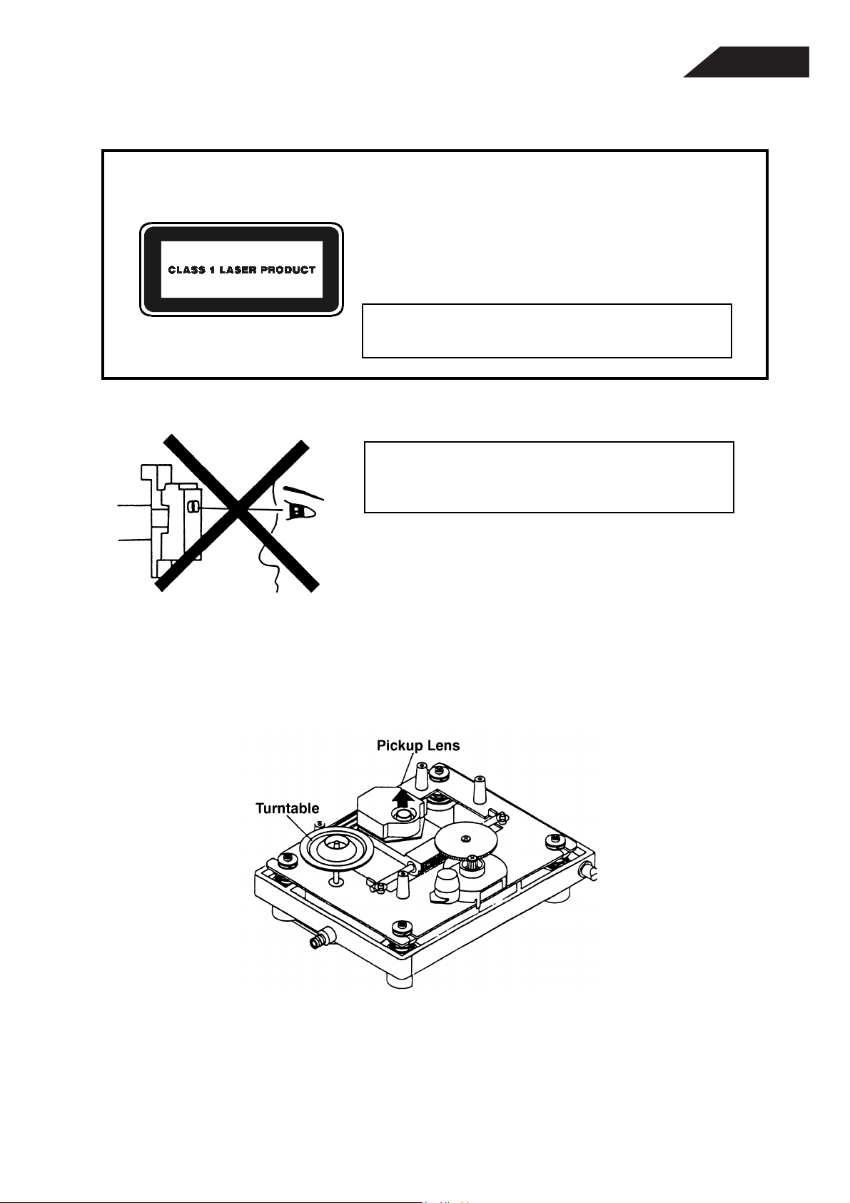
LASER BEAM SAFETY PRECAUTIONS
CLASS 1 LASER PRODUCT
CAUTION
Invisible laser radiation when the unit is open.
Do not stare into beam.
CAUTION: USE OF ANY CONTROLS, ADJUSTMENT, OR
PROCEDURES OTHER THAN THOSE SPECIFIED HEREIN
MAY RESULT IN HAZARDOUS RADIATION EXPOSURE.
Do not look directly at the laser beam
coming from the pickup or allow it to
FL8550
strike against your skin.
This compact disc player uses a pickup that emits a laser beam. The laser beam is emitted from the
location shown in the figure. When checking the laser diode, be sure to keep your eyes at least 1 foot away
from the pickup lens when the diode is turned on. Do not look directly at the laser beam.
CAUTION:
Using controls and adjustment, or doing procedures other than those specified herein, may result in
hazardous radiation exposure.
2
Page 3
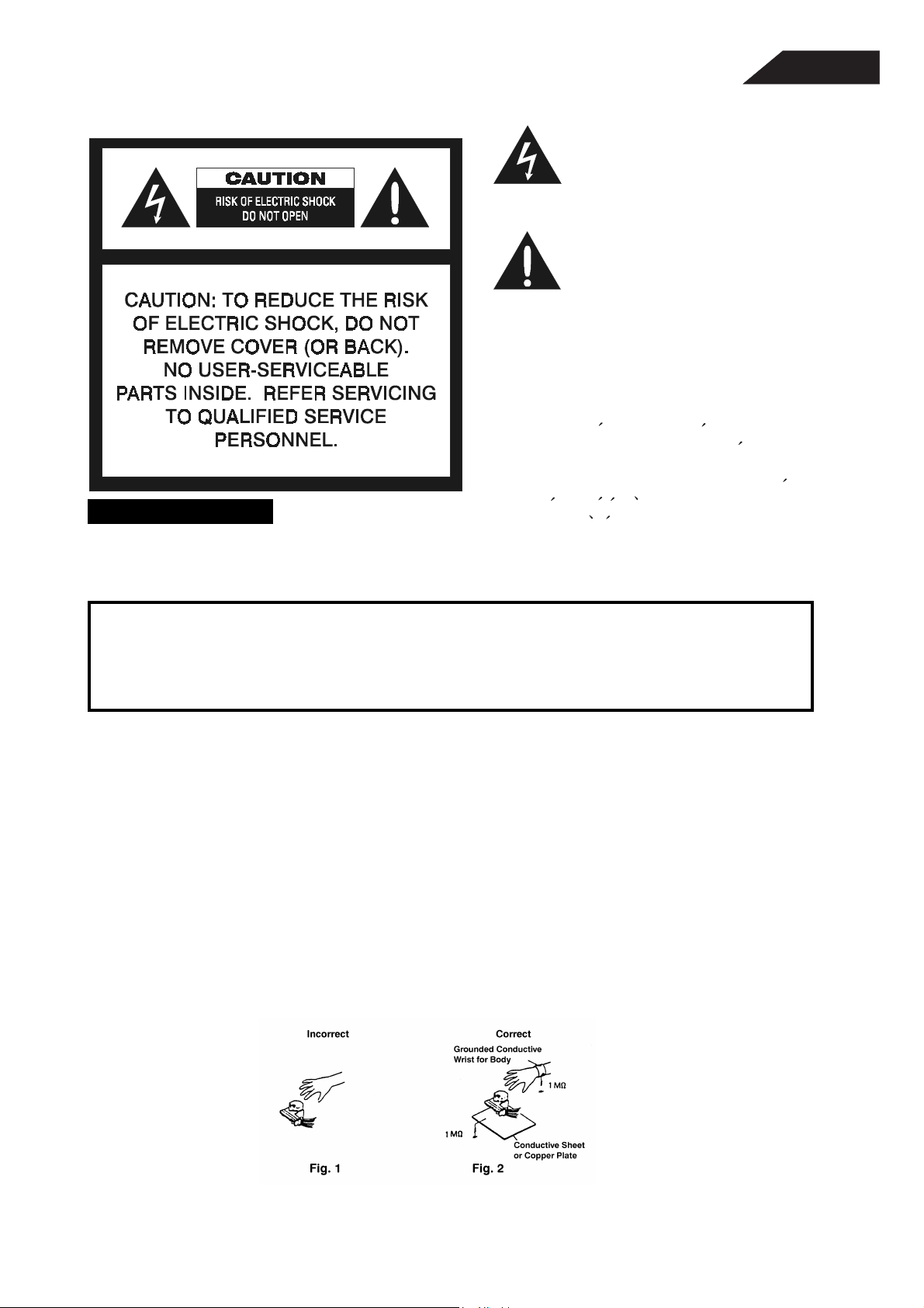
SAFETY PRECAUTIONS
WARNING
To prevent fire or shock hazard, do not
FL8550
This symbol is intended to alert the user to
the presence of uninsulated "dangerous
voltage" within the product's enclosure that
may be of sufficient magnitude to constitute a risk of electric shock to persons.
This symbol is intended to alert the user to
the presence of important operating and
maintenance (servicing) instructions in the
literature accompanying the appliance.
Caution: To p re v e nt e l e ct r i c s h o ck d o not use this
(polarized) plug with an extension cord, receptacle or other outlet unless the blades can be
fully inserted to prevent blade exposure.
Attention: Pour prevenir les chocs electriques ne pas
utiliser cetre fiche polarisee avec un
prolongateur, une prise de courant ou une autre sortie de courant, sauf si les lames prevent
etre inserees a fond-sans en laisser aucune
partie a decouvert.
expose the unit to rain or moisture.
HANDLING LASER PICKUP
The laser diode in the optical system of this player can be damaged by electrostatic discharge from
your clothes or your body. Proper electrostatic grounding for service personal is required during servicing.
BEFORE REPAIRING THE COMPACT DISC PLAYER
Preparation
Human Body Grounding:
Many of the components used in this compact disc player, including the laser pickup, are sensitive to
electrostatic discharge. Service personal should be grounded with an electrostatic armband (1 Mohm).
Caution:
Static charge on clothing does not escape through a body grounding wrist band.
Be careful not to contact the pickup or electrical components with your clothing.
Workbench and Tool Grounding:
A properly-grounded electroconductive plate (1Mohm) or metal sheet should be fitted to the workbench
surface. Tools and instruments (such as soldering irons and scopes) should be grounded to prevent AC
leakage.
Note: Laser diodes are so susceptible to damage from static electricity that, even if a static discharge does
not ruin a diode, it can shorten its life or cause it to work improperly.
3
Page 4

GENERAL INFORMATION
4
1. Power Consumption Operating < 18W; Standby < 5W
2. Power Supply 230VAC 50Hz or 120VAC 60Hz
3. Dimensions 440 x 130 x 386 mm
4. Product Outlook Refer to attached diagram
5. Remote Unit RT03, harman/kardon remote code
6. Compliance Requirement CE LVD EN60065
CE EMC EN55013, EN61000-3-2, EN61000-3-3
NRTL/C
FCC
HDCD
7. Disc Changer Mechanism 5 disc carousel; Play 1 change 4
FL8550
8. Sound Processor HDCD
9. CD Servo System Auto Alignment
AUDIO SPECIFICATION
Typical Limit
Output Level 1KHz 0 dB(no HDCD) 2.0 Vrms ± 1 dB
Frequency Response 20Hz~20KHz reference 1KHz +0-0.5 dB +0.5-1 dB
THD 1KHz 0 dB 30KHz LPF 0.004% 0.01%
THD 20Hz~20KHz 0 dB 30KHz LPF 0.015%
S/N 1KHz 0 dB A-weighted 105 dB 100 dB
Dynamic Range 100 dB 95 dB
Channel Seperation 1KHz 0 dB 95 dB 90 dB
Channel Balance ± 0.5 dB ± 1 dB
De-emphasis ± 0.5 dB ± 1 dB
Maximum Headphones Level 1KHz 0 dB 32 ohm Load 1.5 Vp-p ± 2 dB
Black Dot TCD725A 1000 µm 600 µm
Interruption MCD-131 900 µm 600 µm
Finger Print TCD725A 75 µm 65 µm
Vertical Deviation MCD-151 1.00 mm 0.92 mm
Eccentricity TCD712 140 µm 140 µm
8 cm disc TCD783 Last Track Last Track
Access Time 1st to last track YEDS18 4 sec 10 sec
7
Page 5
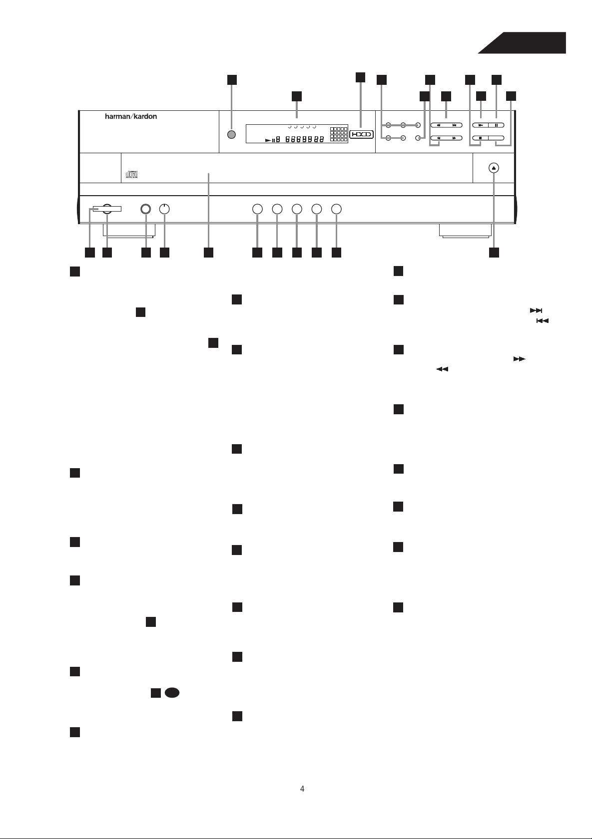
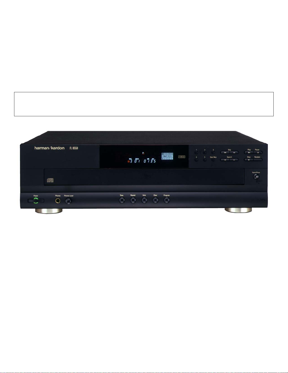
Front Panel Controls
5
21
20
22
18
FL8550
16
15
14
13
12
1719
FL 8550
Power Phones Phones Level
1
2
Power Switch
1
3
4
: Press this switch
5
to change the FL8550 from STANDBY
to ON. When the unit is first
connected to AC power, the
Mode Indicator
2
Status
will turn Amber
(STANDBY mode). Press this switch
to turn the unit ON; indicator will
Green and the
Information Display
20
will illuminate. Press the switch again
to turn the unit off, in STANDBY mode.
When the FL8550 is connected to a
switched AC outlet, such as those
found on the back of many audio
products, when power is applied it will
return to whatever state it was left in
previously, whether ON or STANDBY.
In this case, when always left ON,
further use of the power switch is not
needed.
Status Mode Indicator
2
: When the
FL8550 is in the ON mode, this
indicator will glow green. When the
unit is off, the indicator will glow
amber, indicating that the unit is still
connected to the AC mains supply.
3
Headphones Jack
: Connect a set
of standard headphones to this jack
for private listening.
4
Headphones Level
: Turn this
knob to increase or decrease the
volume level for headphones
connected to the FL8550's
Headphones Jack
3
. Note that
changing this level will not change the
sound level for the unit's main output,
as that remains constant.
CD Drawer
5
: This drawer holds the
discs that will be played. Press the
Open/ Close
button to open
11
1
the drawer so that discs may be
inserted.
Time Button
: In normal operation,
this display will show the running time
of the track being played. Press the
button once to check the time
remaining for the track in play. Press
321
Disc Skip54
DISC TRACK
1 32 4 5
INTRO
MIN
SEC
PROGRAM
RANDOM
ALL 1 DISCS
REPEAT 1A-B
Time Repeat Intro Clear Program
3
1
2
4
5
6
7
8
9
10
11
13
12
14
15
16
18
17
19
20
667 8 9 10 11
this button again to view the total play
time remaining for the disc in play.
7
Repeat Button
: Press this button
once to constantly repeat the track
currently being played. Press it a
second time to repeat the entire disc.
Intro Button
8
: Press this button to
put the FL8550 in the Intro Scan
mode. When you press the button,
the unit will play the first 10 seconds
of each track on the disc, and then
Stop Button
15
stop the disc currently being played.
16
Skip Button
this button to move to the next track ,
or to move back to the previous track
on the disc being played.
Search Button
17
of this button to search forward or
backwards through a disc to
locate a particular portion of the
selection of the disc being played.
move to the next track. Press the
Disc Skip Button
button again to defeat the function
and continue full play of the current
track.
18
button to change to the next disc. If a
disc position is empty, the FL8550 will
automatically search for the next
9
Clear Button
: Press this button to
position that contains a disc.
remove tracks from a programmed
Disc Select Buttons
sequence. Each press of the button
will remove one track, starting with
the last track programmed to play.
Program Button
10
: This button is
used to program the playback of a
disc in a particular order.
Open/ Close
11
open or close the disc drawer. DO
: Press this button to
NOT push the drawer to close it, or
damage to the transport mechanism
may result.
Random Button
12
: Press this
button to put a disc into play, and to
have all of the tracks played in a
19
of these buttons to select the disc in a
specific position in the CD drawer.
20
Information Display
provides details about the operation
of the FL8550.
Remote Sensor
21
behind this window receives
commands from the remote control.
Keep this area clear if you wish to use
the FL8550 with a remote control.
22
HDCD Indicator: This LED will light
automatically when a CD with HDCD
encoding is playing.
random order.
Pause Button
13
: Press this button
once to momentarily pause a disc.
When the button is pressed again, the
disc will resume play at the point it
was paused.
Play Button
14
: Press this button to
start the playback of a CD. If the CD
drawer is open, pressing this button
will automatically close the drawer.
PausePlaySkip
Stop RandomSearch
Open/Close
: Press this button to
: Press either side of
: Press either side
: Press this
: Press one
: This display
: The sensor
4
Page 6
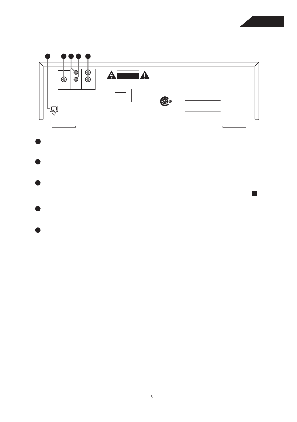
Rear Panel Connections
6
2 4 531
FL8550
(YCL).
MODEL NO: FL8550
HARMAN KARDON
NORTHRIDGE
CALIFORNIA, U.S.A.
MADE IN CHINA
LEFT
IN
RIGHT
OUT
DIGITAL
OUTPUT
This device complies with part 15 of the FCC Rules.
Operation is subject to the following two conditions:
(1) This device may not cause harmful interference,
AC INPUT
AC 117V / 60Hz
1
and (2) this device must accept any interference
received, including interference that may cause
20W
undesired operation.
AC Power Cord
OUTPUTREMOTE
AUDIO
CAUTION
RISK OF ELECTRIC SHOCK
RISK OF ELECTRIC SHOCK
DO NOT OPEN
SHOCK HAZARD : DO NOT OPEN.
SHOCK HAZARD : DO NOT OPEN.
AVIS:RISQUE DE CHOC ELECTRIQUE-NE PAS OUVRIR.
AVIS:RISQUE DE CHOC ELECTRIQUE-NE PAS OUVRIR.
WARNING: "TO REDUCE THE RISK OF FIRE OR
ELECTRIC SHOCK, DO NOT EXPOSE THIS APPLIANCE
TO RAIN OR MOISTURE."
DO NOT OPEN
SERIAL NO.
NRTL/C
LR46800
CSA 22.2
UL 1270
PRODUCT COMPLIES WITH DHHS
RULES 21CFR SUBCHAPTER J,
APPLICABLE AT DATE MANUFACTURED:
Connect this plug to an AC outlet. If the outlet is switch is controlled, make certain that the switch is in the ON
position.
2
Coaxial Digital Output
Connect this jack to the coaxial digital input of an external digital-to-analog converter for direct access to the digital
signals of the FL8550. DO NOT connect this jack to the standard audio inputs of any device.
3
Remote Control Input
Connect the output of a remote infrared sensor or the remote control output of another compatible Harman Kardon
product. This will enable the remote control system to operate even when the front panel is
Remote Sensor
21
blocked. It will also allow use of the FL8550 with optional, external control systems.
4
Remote Control Output
Connect this jack to the input of another compatible Harman Kardon remote controlled device to have the remote
sensor on the FL8550 provide signals to other products.
5
Fixed Audio Outputs
Connect these jacks to the CD audio inputs of your receiver, surround processor or preamplifier.
5
Page 7
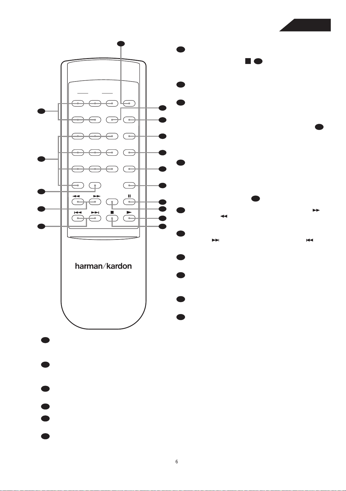
Remote Control Functions
7
1
FL8550
. Press this button to open or close
Open/ Close Button:
1
the disc drawer. The drawer may also be closed by
pressing the button . DO NOT push the
drawer, as damage to the transport mechanism may
result.
Play
14
8
Disc Select Buttons:
2
DISC NO.
1 2 3
2
4 5
DISC
SKIP
OPEN/
CLOSE
REPEAT
16
15
PROGRAM321
14
4 5 6 CLEAR
13
3
TIME987
12
+10 INTRO
10
11
4
RANDOMSEARCH
10
5
SKIP
9
8
6
7
select the disc in a specific position in the CD drawer.
Numeric Buttons:
3
specific track on a disc. The FL8550 will immediately
search for the track and begin to play it. For tracks 1
through 10 on a disc, you need only press the desired
number. For tracks 10 and above, press the button
to select the first digit of the track number, and then
press the second digit from these numeric buttons.
These buttons are also used to enter track numbers into
the memory for pre-programmed play lists.
+10 Button:
4
track number above 10. Each press of the button
increases the first digit one increment. Press it once to
start accessing tracks 10 through 19 twice to start
accessing tracks 20 through 29, and so forth. For
example, to select track 22, press the button twice,
and then press the button .
Search Buttons:
5
or backwards through a disc to locate a particular
portion of the selection being played.
Skip Buttons:
6
next track , or to move back to the previous track
on the disc being played.
Press this button to select the first digit of a
Press one of these buttons to
Press these buttons to select a
10+
+10
2
Press these buttons to search forward
Press one of these buttons to move to the
3
4
7
FL 8550
11
Intro Button:
play the first 10 seconds of each track on the disc, and then move to the next track. Press the button again to defeat
the function and continue full play of the current track.
Time Button:
12
of the track being played. Press the button once to check the time remaining for the track in play. Press the button a
third time to view the total play time remaining for the disc in play.
Clear Button:
13
remove one track, starting with the last track programmed to play.
Program Button:
14
Repeat Button:
15
to repeat the entire disc.
Press this button to put the FL8550 into the Intro Scan mode. When you press this button, the unit will
Press this button to select the time display. In normal operation, the display will show the running time
Press this button to remove tracks from a programmed sequence. Each press of the button will
This button is used to program the playback of a disc in a particular order.
Press this button once to constantly repeat the track currently being played. Press it a second time
Stop Button:
being played.
Play Button:
8
CD. If the CD drawer is open, pressing this button will
automatically close the drawer.
Random Button:
9
and to have all of the tracks played in a random order.
Pause Button:
10
stop a disc. When the button is pressed again, the disc
will resume play at the point it was stopped.
Press this button to stop the disc currently
Press this button to start the playback of a
Press this button to put a disc into play,
Press this button once to momentarily
Disc Skip Button:
16
automatically search for the next position that contains a disc.
Press this button to change to the next disc. If a disc position is empty, the FL8350 will
6
Page 8

Troubleshooting Guide
8
SYMPTOM
CAUSE
FL8550
SOLUTION
No lights on front panel
Remote does not appear
to operate
Front panel lights, but CD
does not play
Play indicator lights, but
no sound is heard
Sound skips or stutters
during play
Sound is continually distorted
• No AC power
• Main Power Switch turned off
• Weak batteries
• Blocked sensor
• Disc upside down
• Moisture inside unit
•Poor connections
• Wrong source selected
• Disc may be damaged
• Surface vibrations
• Incorrect input
• Make certain that the AC power cord is plugged into
a live outlet.
• Turn on Main Power Switch.
• Install fresh batteries, observing polarity indications.
• Remove obstructions from the front panel sensor or
connect a remote sensor to the
on the rear panel.
• Reload disc with label side facing up.
• Leave the unit turned ON for 30 minutes to allow
moisture to evaporate.
• Make certain connections are secure and made
to the correct (e.g.,
• Select CD source on receiver or preamp.
• Try another disc.
• Isolate the unit from vibration by placing it on a
firm surface or move it further away from speakers.
• Make certain that the FL8550 is connected to a linelevel audio input, NOT a digital audio or phono input.
CD) input.
Remote In jack
Page 9

9
harman/kardon
Service Bulletin
Service bulletin # H/K9901 Rev1 November 2002
Warranty Labor Rate: Major Repair
To: All harman/kardon Service Centers
Models: FL8350/FL8550
Subject: “No disc” reading in display
When a CD is in the carousel at the play position, Infra red light emitted by IR LED D3 is reflected onto IR Photo
sensor D2. D3 and D2 are on the PCB located underneath the carousel. When the amount of IR light received
by D2 is insufficient, D2 will not saturate and the display will read “No disc”.
In the event you receive an FL8350 or FL8550 with the complaint: Display reads “No disc” but a disc is in
the tray, perform the modification as listed below:
Lay the unit on a padded surface.
1)
2)
Remove the (7) Black Philips screws holding the Top Cover on; remove cover.
3)
Lay unit on its side and remove (5) Black screws on bottom which hold front panel to chassis.
4)
Lay unit upright, remove (2) Black screws at top front section holding front panel to the front tray retainer brackets.
5)
Pull front panel away, cut plastic cable ties if necessary, and lay the front panel face down on the table.
6)
Remove (4) tray retainer brackets, (1) Plated screw each. (Bracket on left side may have a ground terminal).
7)
Pull the carousel tray up and out of the unit; turn upside-down to expose the sensor board.
8)
Remove the (2) Plated screws holding the sensor board to tray.
9)
Lift the board and unplug either molex connector CN1 or CN2 to be able to turn board upside-down.
10)
Locate R1 and change from a 470Ω to a 750Ω resistor - h/k part# 1007-501316-000.
11)
Locate R2 and change from a 750Ω to a 470Ω resistor - h/k part# 1004-701316-000.
Alternately, the two above parts may just be “swapped”, as this will result in the correct values.
12) Locate D3 and replace with new infra-red LED - h/k part# 3100-204000-002.
REASSEMBLY:
13) Replace sensor board, screws, and CN1 or CN2 connectors.
14) Turn the carousel tray over and replace back in the track; tray must be positioned all the way at the rear of the unit.
When placed correctly, tray should not glide back & forth on the track.
15) Replace and attach the (4) tray retainer brackets with single screws - ground wire (if present) is re-attached to left
front bracket.
16) Replace the front panel, both with the (5) bottom screws and the (2) screws at the top. Note: Make sure any
washers that were present between the various brackets and the chassis are reinstalled. Replace cable ties as
necessary.
17) Test the player by inserting one or more compact discs, assure unit reads discs in all slots.
18) Locate MCU board, which is mounted vertically on right side of unit. Connect DC Multimeter to Pin 8 (gray wire) of
CN705 (10 pin plug, labeled 'DSNS'), and Pin 2 (red wire) of CN701 (2 pin plug). While playing a disc, DC Multimeter
reading must be between 4.7 V and 5.0 V.
19) Replace top cover and screws.
Model Serial number (120V) Serial number (230V) Status Action
FL8350
FL8550
FL8350
FL8550
YC0001-01001
to
YC0001-37014
YC0003-01001
to
YC0003-08666
YC0001-37015
and above
YC0003-08667
and above
YC0002-01001
to
YC0002-16673
YC0004-01001
to
YC0004-04884
YC0002-16674
and above
YC0004-04885
and above
Needs Modification
Changed by factory
R1 with
R2 with 470 Ω
NONE REQUIRED
Replace:
750 Ω
D3
Page 10
harman/kardon
10
Service bulletin # H/K2000-09 November 2000 This is considered a Minor Repair
To: All harman/kardon Service Centers
Models: FL8350/FL8550
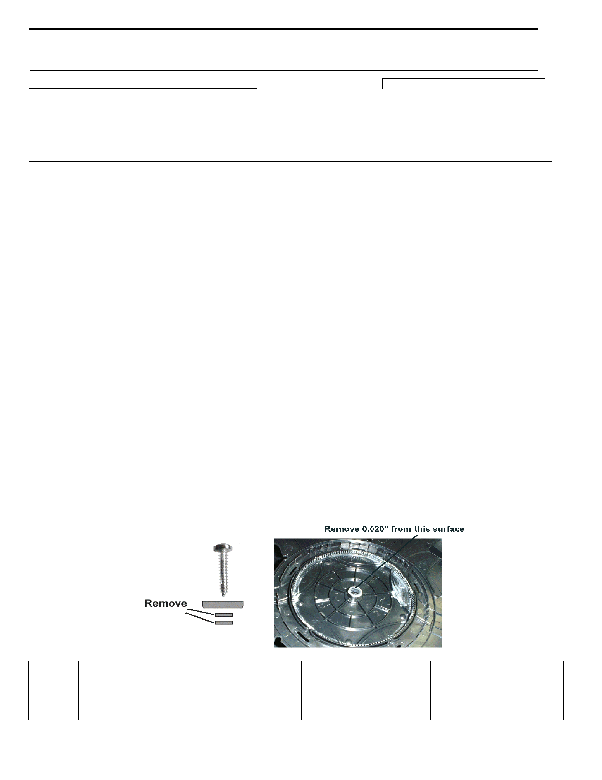
Subject: Carousel does not stop
In the event you receive an FL8350 or FL8550 with the complaint: “The carousel does not stop at a given
disc position, …or passes disc positions intermittently”, perform the modification listed below:
1) Lay the unit on a padded surface.
2) Remove the (7) Black Philips screws holding the Top Cover on; remove cover.
3) In the center of the carousel are a single screw and plated washer; remove these.
4) Underneath the larger plated washer are two smaller fiber washers. These are to be removed permanently.
5) Examine the larger plated washer carefully. Upon replacement of the larger plated washer and screw, make
sure the slightly sharper, stamped edge of the washer is facing upwards.
6) Test the player by inserting one or more compact discs, assure the unit reads discs in all slots, and stops at
all positions.
IF THIS MODIFICATION DOES NOT CORRECT THE PROBLEM
7) Lay unit on its side and remove (5) Black screws on the bottom, which hold the front panel to the chassis.
8) Lay unit upright, remove (2) Black screws at top front section holding front panel to the front tray retainer
brackets.
9) Pull front panel away, cut plastic cable ties if necessary, and lay the front panel face down on the table.
10) In the center of the carousel, once again remove the single screw and plated washer.
11) Lift the carousel up and off the chassis, towards the front of the unit.
12) Turn the carousel upside-down; in the center is a hollow plastic post. Remove any excess lubricant with a
clean dry cloth or paper towel, saving it for re-application. The end of this post must be filed down
approximately 0.020” (0.5mm) with a file, Dremel tool, or similar tool. Be sure not to remove too much
material and keep the surface even (flat). Remove any debris or shavings when finished.
13) Spread and replace the saved lubricant on the new surface of the center post.
Service Bulletin
REASSEMBLY:
14) Replace the carousel and mounting screw + washer.
15) Replace the front panel, both with the (5) bottom screws and the (2) screws at the top. Note: Make sure any
washers that were present between the various brackets and the chassis are reinstalled. Replace cable ties
as necessary. Replace the top cover.
16) Test the player by inserting one or more compact discs, assure unit reads discs in all slots, and stops at all
positions.
Model Serial number (120V) Serial number (230V) Status Action
Remove small fiber washers
FL8350
FL8550
All Serial numbers
affected
All Serial numbers
affected
May need modification
in center screw of carousel; if
necessary file center post
down 0.020” (0.5mm)
harman/kardon Incorporated 250 Crossways Park Drive, Woodbury New York 11797 (516) 496-3400
Page 11
11
harman/kardon
Troubleshooting tips and solutions to common service problems
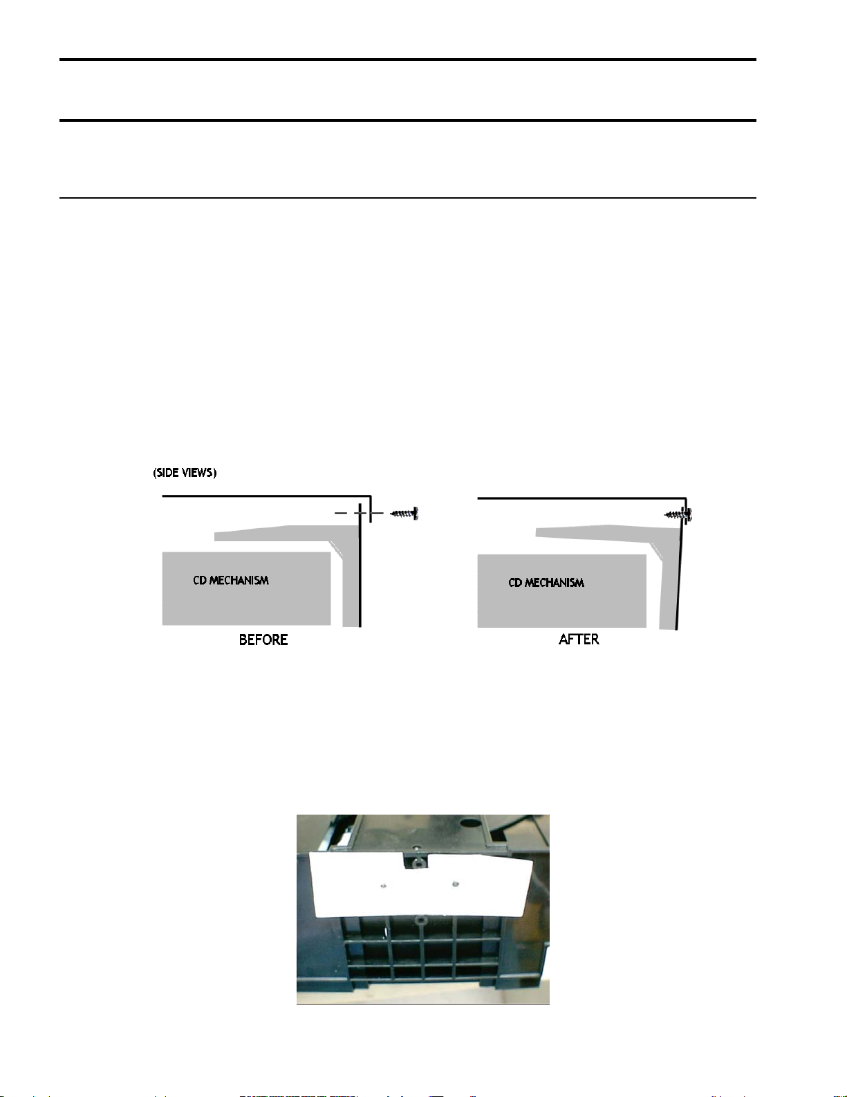
For models: FL8350/FL8550/FL8380 TIP# HKTT2003-06
Complaint: Unit Will Not Play or Recognize a Disc, “Skipping”.
Possible Problem: Misalignment of the top cover and rear panel.
To test, attempt to play the unit with the top cover OFF. If symptoms persist, troubleshoot further. If the
unit will play with the cover OFF, the problem is caused by a misalignment of the top cover and the rear
panel. When the screws are tightened on the top cover, at the rear of the unit, the CD mechanism may
“warp” upward in the area of the clamper arm, which causes a “Will not Play” symptom, which shows up as
an unusual delay, with the word “Disc” in the display, after the “Play” button is pressed.
TECH TIPS
Solutions:
Washers can be added to the top rear screws to fill the gap between the top cover “lip” and rear panel.
Alternately, a spacer can be constructed of fish paper, plastic sheet, or similar material, that will fit
between the Disc Clamper and the inside of the rear panel. Choose thickness as necessary.
Page 12

FL8550
12
Page 13
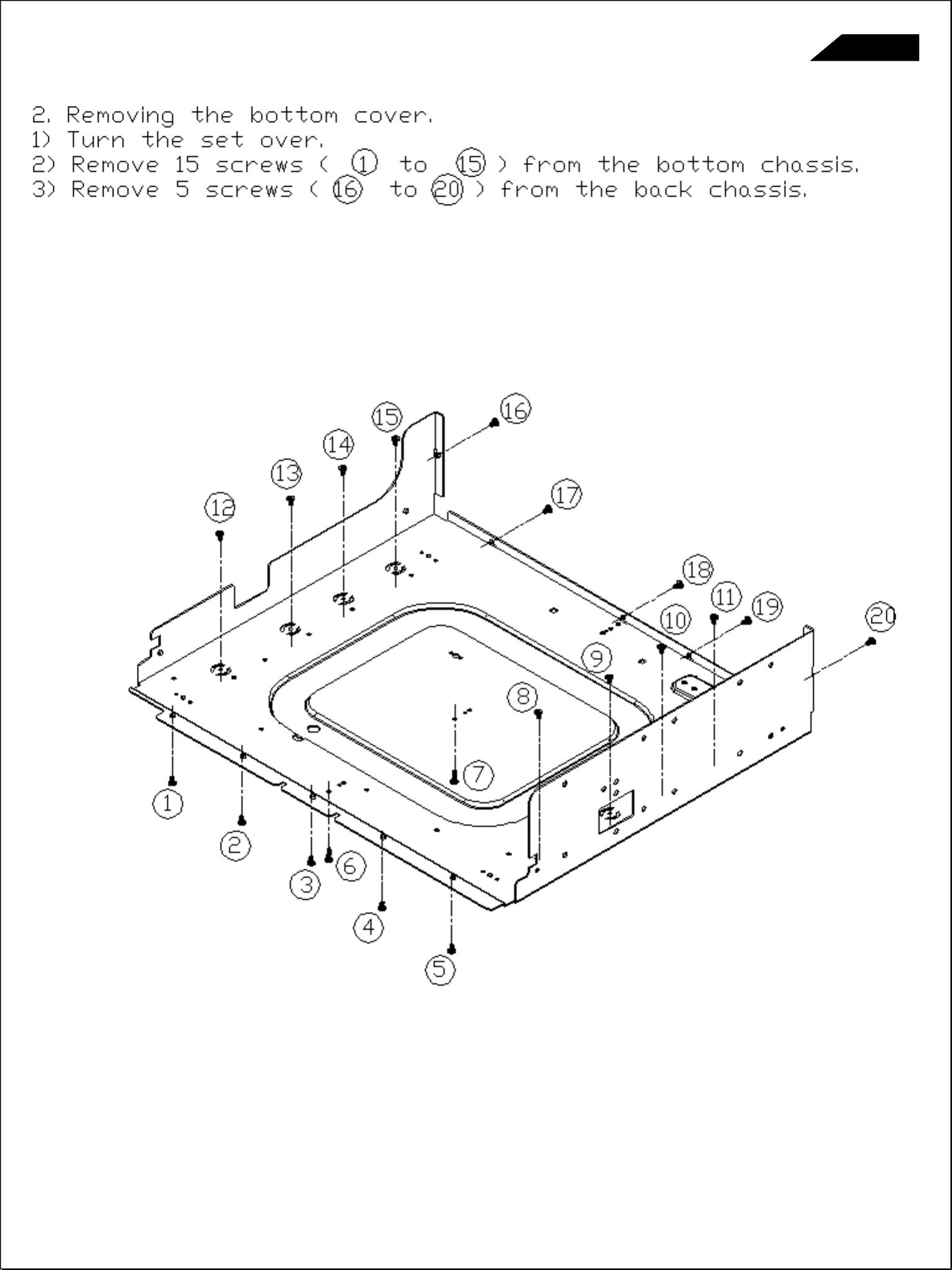
FL8550
13
Page 14
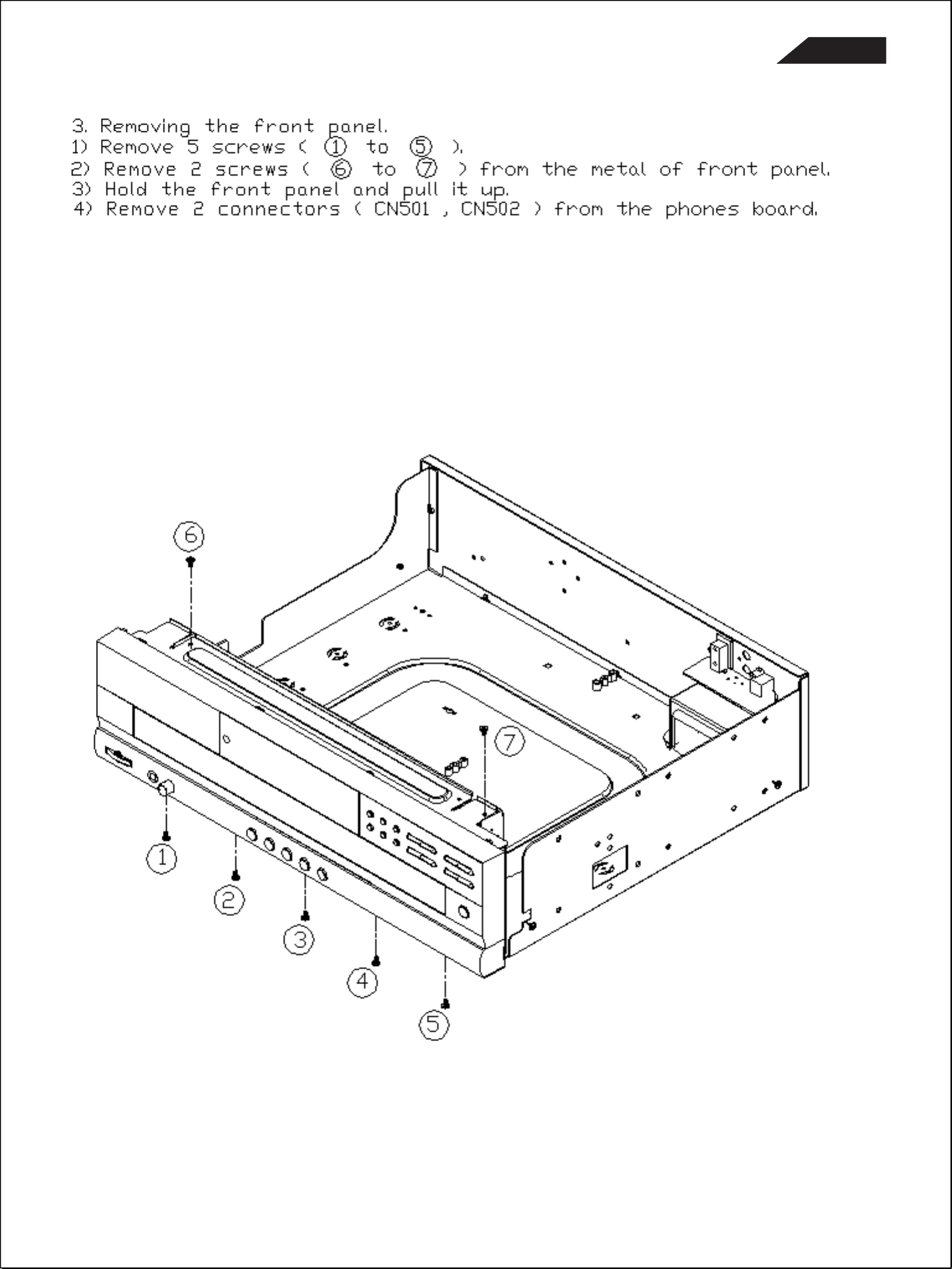
FL8550
14
Page 15
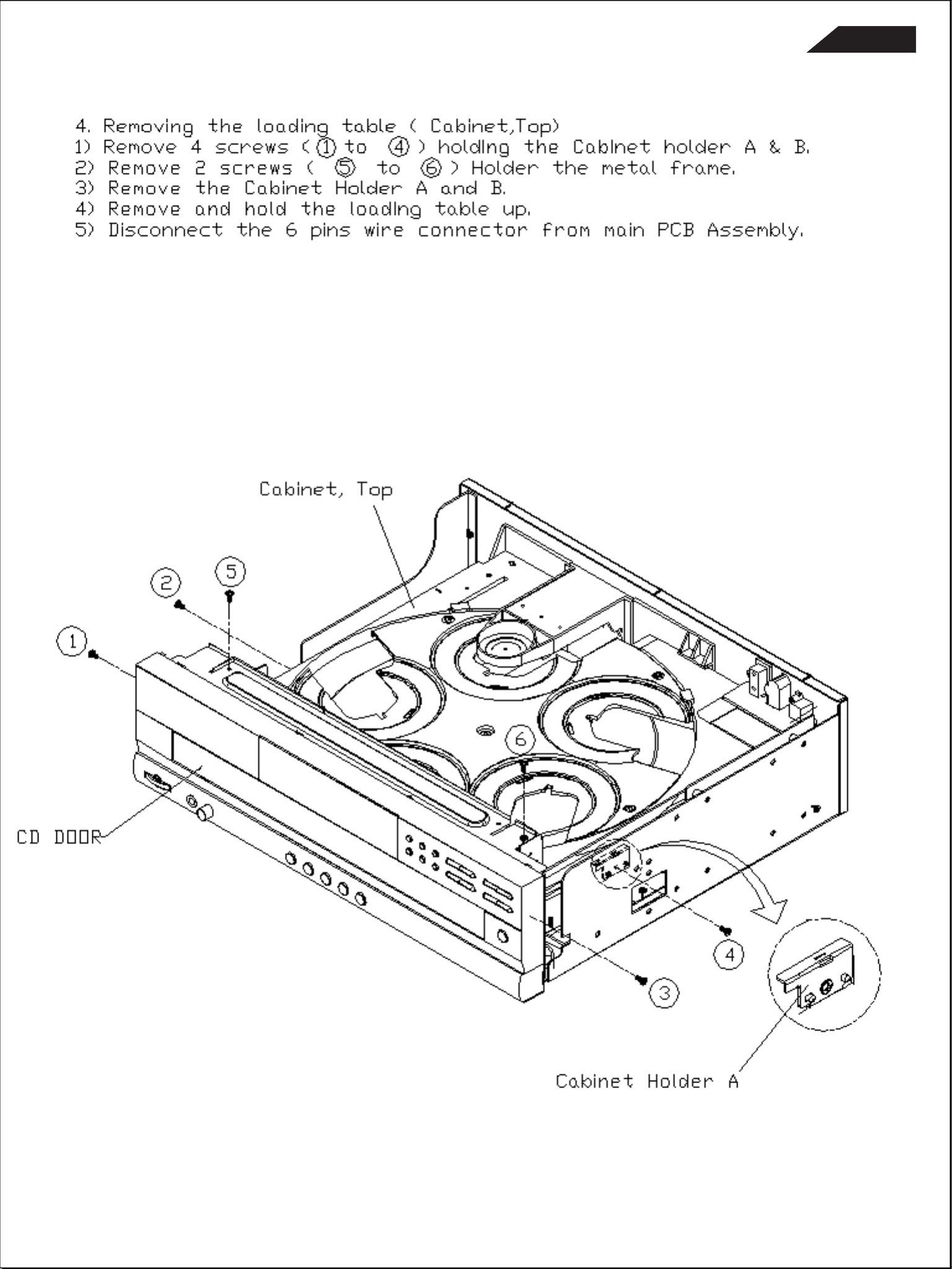
15
FL8550
Page 16
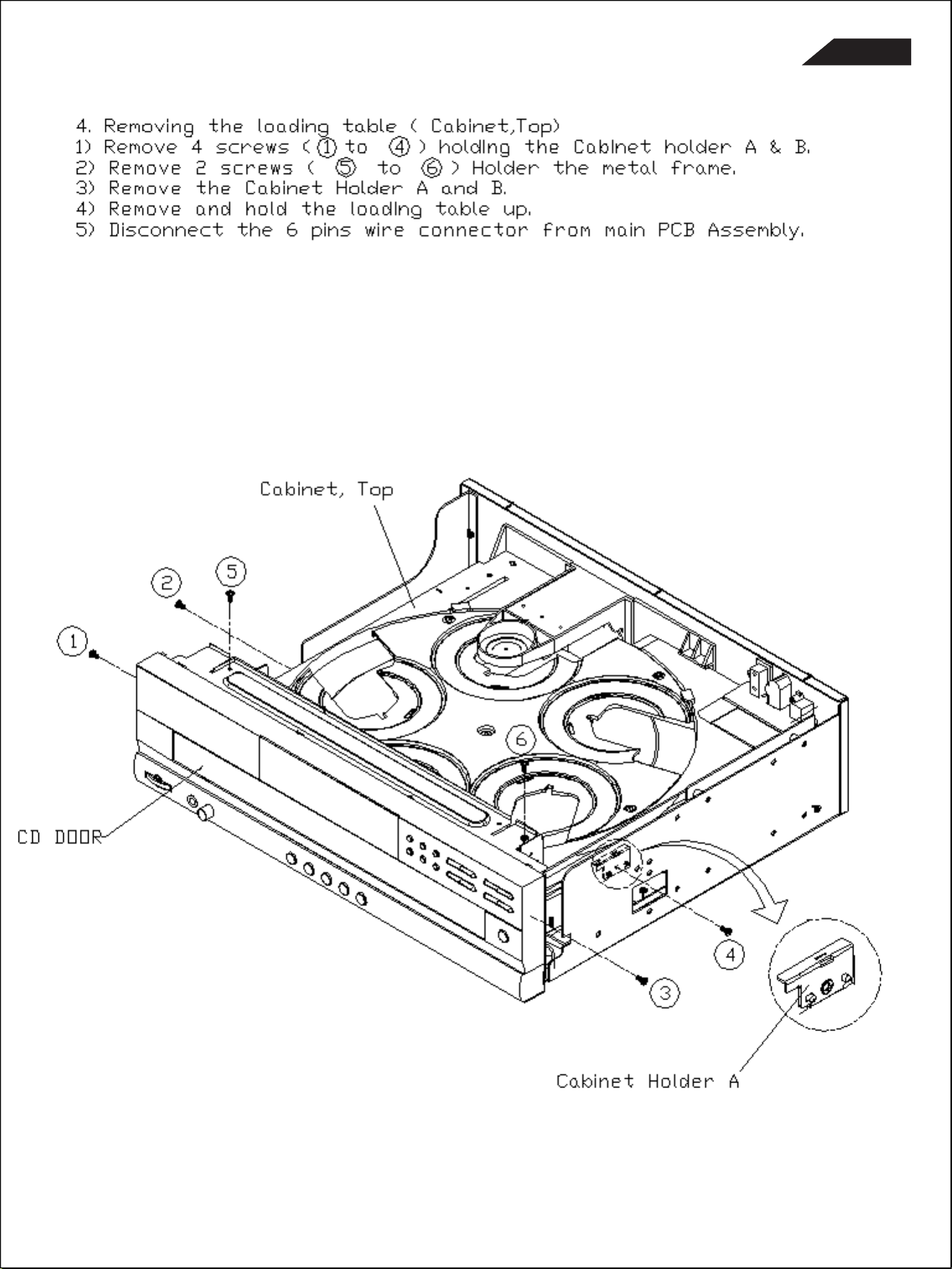
FL8550
16
Page 17
FL8550
17
Page 18

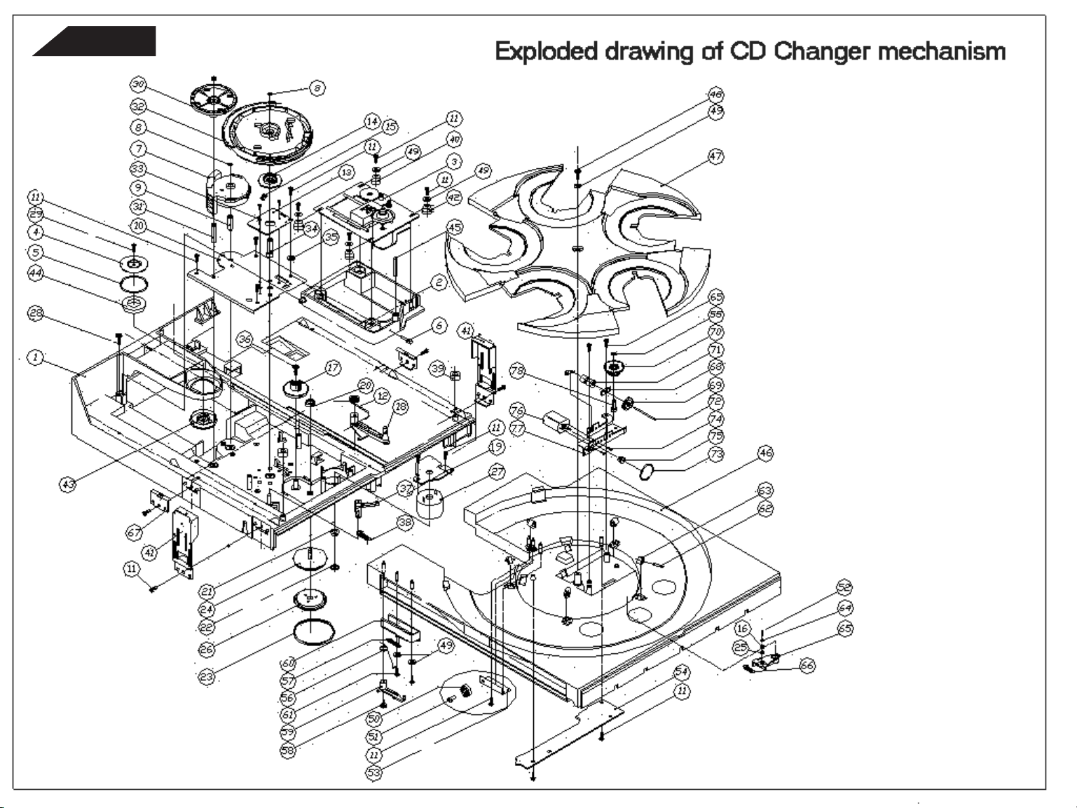
FL8550 Exploded Drawing List
18
Seq. No. Part Number Description Qty
1 6583-510002-000-01 TOP CABINET, PAINTED 1.0
2 6583-510004-001 BRACKET, FRONT PANEL 1.0
3 6083-510002-000-01 HARMAN/KARDON FL8350&FL8550 TRAY DOOR(WSILKSCREEN) 1.0
4 9483-501000-111 FL8350 POWER CONTROL BOARD ASSY REV A 1.0
5 6600-010293-000 SPRING, POWER SWITCH 1.0
6 6083-510008-000 *LENS, POWER KNOB 1.0
7 6083-5100015-000 LIGHT SHEET BLACK 1.0
8 6083-510007-000-01 KNOB, POWER PAINTED 1.0
10 6583-510006-000 BRACKET, PHONES (MIC) 1.0
11 7107-212005-022 WASHER M7 1.0
12 7112-517506-022 WASHER M12 1.0
13 6600-120120-000 NUTS M12 1.0
14 6600-120070-000 NUTS M7 1.0
15 6083-510006-000-01 KNOB VR PAINTED 1.0
16 6083-510005-000-01 KNOB, PROGRAM PAINTED 1.0
17 6083-510001-002-02 HARMAN/KARONT FRONT PANEL W/SILKCREEN&P 1.0
18 6083-510003-000-01 HARMAN/KARDON FL8550 DISPLAY LENS (W SILKSCREEN) 1.0
19 6083-510004-000-01 KNOB, DISC PAINTED 1.0
20 9485-801000-261 FL8550 DISPLAY BOARD (VFD) ASSY REV A 1.0
21 6083-510010-000-01 HARMAN/KARDON FUNCTION KNOB (W SILKSCREEN&PAINTED) 1.0
22 6083-510009-000-01 HARMAN/KARDON 'EJECT' KNOB (W SILKSCREEN&PAINTED) 1.0
23 6583-510001-001 BOTTOM CABINET 1.0
24 6029-010012-000-01 PLASTIC FOOT (HOT STAMPING) 4.0
25 6600-070003-000 CD90R05 RUBBER PAD,LEG 4.0
26 6083-510014-000 *BRACKET, 5CD-SIDE 2 1.0
27 9483-501000-232 FL8350 MCU BOARD 1.0
28 6600-020010-000 CD420L01 PCB MOUNT. 4.0
29 9485-501000-291 FL8550 DIGITAL OUTPUT BOARD 1.0
30 6600-180007-000 AC CORD BUSHING (PG5RF-5B) 1.0
31 6600-120040-000 SCREW NUT M4X7X3 2.0
32 7104-010010-022 WASHER M4X10X1MM 3.0
33 3200-480140-401 TRANSFORMER EI48 117V CUL #4801Y44T-1 (WINBOND) 1.0
34 9485-501000-013 FL8550 CD MAIN BOARD ASSY 1.0
35 9600-505004-002 5CD MECHA ASSY FOR FL8350 REV B 1.0
36 6083-510013-000 *BRACKET, 5CD-SIDE 1 1.0
37 6083-510011-000 STAND, FRONT-5CD 2.0
38 6083-510012-000 STAND, REAR-5CD 1.0
39 2610-218300-002 AC POWER CORD NON-INTEGRAL SPT-2 UL/CSA 1.0
40 6583-510003-001-03 HARMAN/KARDON FL8550 R/P (117V FCC&CSA VR) 1.0
A 7003-006001-111 SCREW M3X6 S.T.P. B/H (BLACK) 22.0
B 7003-006002-112 SCREW M3X6 P.T.P. B/H 23.0
C 7003-008002-112 SCREW M3X8 P.T.P. B/H 16.0
D 7002-606010-062 SCREW M2.6X6 W/H 8.0
E 7004-010010-112 SCREW M4X10 B/H 2.0
F 7003-016002-112 SCREW M3X16 PTP B/H ZN 3.0
FL8550
Page 19

5CD EXPLODED DRAWING LIST
DC MOTOR MABUCHI RF-500TB-14415 (DC002VT00003)
19
SEQ NO.
1 6005-050050-007 BASE, 5CD 1.0
2 6005-050010-004 BRACKET, CD MECHA 1.0
3 3009-901000-000 SANYO CD MECHANISM CD90V1 1.0
4 6590-050001-001 CD90 CHUCKING METAL PLATE 1.0
5 6600-140001-000 CD90F01 CHUCKING METAL PLATE FELT RING 1.0
6 6600-020200-002 PIN, ROUND 1.0
7 6005-050008-001 CONTROL CAM 1.0
8 7105-010005-030 WASHER LOCK 5X10X0.5MM 3.0
9 6600-020198-000 5CD PIN, CONTROL CAM 1.0
10 6505-050001-001 BRACKET GEAR 1.0
11 7003-008002-112 SCREW M3X8 B TYPE B/H ZN 12.0
12 6600-010211-000 5CD SPRING, LEVER LOCK, OUTER 1.0
13 4841-010700-006 TURNTABLE PCB REV. F 1.0
14 6005-050025-002 SWITCH COVER 1.0
15 6505-050007-001 CONTACT PLATE 1.0
17 6005-050009-000 INTERMEDIATE GEAR 1.0
18 6005-050014-004 LEVER LOCK, OUTER 1.0
19 4800-310210-001 LOADER BOARD VER A 1.0
20 6005-050011-000 IDLER GEAR 1.0
21 6005-050023-001 PULLEY MOTOR 1.0
22 6005-050024-000 PULLEY DISC 1.0
23 6600-090053-000 5CD BELT MOTOR LOADING 1.0
24 6005-050013-001 DRIVEN PULLEY (WHITE) 1.0
25 6005-050027-000 BUSH, ROLLER 1.0
26 6005-050012-000 DRIVEN PULLEY PLATE 1.0
27 RF-500TB-14415
28 7003-012002-062 SCREW M3X12 P.T.P. W/H 1.0
29 7002-605005-112 SCREW M2.6X5 CLASSI B/H ZN 1.0
30 6005-050007-000 GEAR, CABINET TOP 1.0
31 6600-020197-001 PIN CABINET TOP 1.0
32 6005-050006-004 CONTROL CAM 1.0
33 7002-006001-022 SCREW M2*6 S.T.P. P/H 2.0
34 6600-020196-002 PIN, CAM CABINET 1.0
35 7103-012010-022 WASHER M3X12X1MM 1.0
36 7003-008002-062 SCREWM3X8 P TYPE W/H ZN 1.0
37 6005-050015-000 LEVER LOCK 1.0
38 6600-010210-000 SPRING LEVER LOCK 1.0
39 6600-170021-000 5CD CUSHION RING 2.0
40 6600-170019-000 5CD CUSHION B 2.0
41 6600-020181-000 5CD SCREW, SPECIAL 4.0
42 6600-170018-000 5CD CUSHION A 2.0
43 6090-050002-004 CD90 CHUCKING PULLEY 1.0
44 6600-150006-001 CHUCKING MAGNET 1.0
45 6600-020199-001 PIN, LOCK 1.0
46 6005-050002-011 CABINET TOP 1.0
47 6005-050001-006 TRUNTABLE 1.0
48 7003-012002-062 SCREW M3X12 P.T.P. W/H 1.0
49 7103-012010-022 WASHER M3X12X1MM 1.0
50 6005-050017-000 ROLLER 1.0
51 6600-020202-000 5CD PIN, ROLLER 1.0
PART NO. DESCRUPTION QTY.
1.0
FL8550
Page 20

52 6600-020297-000 PIN ROLLER LOCK 1.0
20
53 6505-050005-001 BRACKET ROLLER 1.0
54 9400-501000-132 5CD SENSOR BOARD ASSY REV B 1.0
55 7103-006005-130 WASHER 3X6X0.5MM CUT 1.0
56 6600-010213-000 5CD SPRING, GEAR BLOCK ARM 1.0
57 6600-010212-002 5CD SPRING, GEAR BLOCK 1.0
58 7002-620002-062 SCREW M2.6X20 P TYPE W/H ZN 1.0
59 6005-050005-001 GEAR BLOCK ARM 1.0
60 6005-050004-003 GEAR BLOCK 1.0
61 7002-608002-002 SCREW M2.6X8 P.T.P W/H D6.5 2.0
62 6600-020203-000 5CD SHAFT, T.T. ROLLER 5.0
63 6600-080001-000 YN21R D03/04 PINCH ROLLER 5.0
64 6005-050028-000 WASHER, BUSH 1.0
65 6005-050026-002 LEVER LOCK, T.T. 1.0
66 6600-010290-001 SPRING LEVER LOCK 1.0
67 6505-050002-001 CABINET HOLDER A 2.0
68 6005-050019-000 SHAFT BUSHING 2.0
69 6005-050020-000 PULLEY ROTARY 1.0
70 6005-050021-000 GEAR ROTARY 1.0
71 6005-050022-000 GEAR WORM 1.0
72 6600-020268-000 SHAFT DIA. 2X34MM 1.0
73 6600-090052-000 5CD BELT ROTARY 1.0
74 7002-003010-111 SCREW M2X3 B/H (BLACK) 2.0
75 6005-050018-000 MOTOR PULLEY 1.0
76 FF130SH11340-2684A MOTOR FF-130SH-11340-02684A (MABUCHI) 1.0
77 6505-050004-004 MOTOR BRACKET 1.0
78 6600-020201-001 SHAFT GEAR ROTARY 1.0
79 6505-050003-001 5CD CABINET HOLDER B 2.0
FL8550
Page 21
ADJUSTMENT PROCEDURES
21
Reference Disk for adjustments: Sony YEDS - 18
Mode: FL8550
Testing Equipment:
i. 5020 Frequency Response Analyzer
ii. Oscilloscope
iii. Frequency Counter
iv. Frequency Generator (Kenwood AG-203A)
FL8550
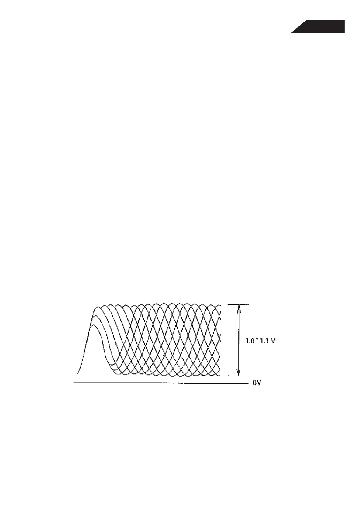
Adjustment Procedure
(A) Focus Adjustment
i. Connect Jitter Meter between TP1 (R51) and Vref (J6), then play a CD disc.
ii. Adjust VR1 until Jitter Meter get the minimum point.
iii. Connect Oscilloscope as the same as the last step. Waveform will be read as
diamond shape and voltage is about 1.1v as perfect. (see the figure 1)
Fig. 1
Page 22
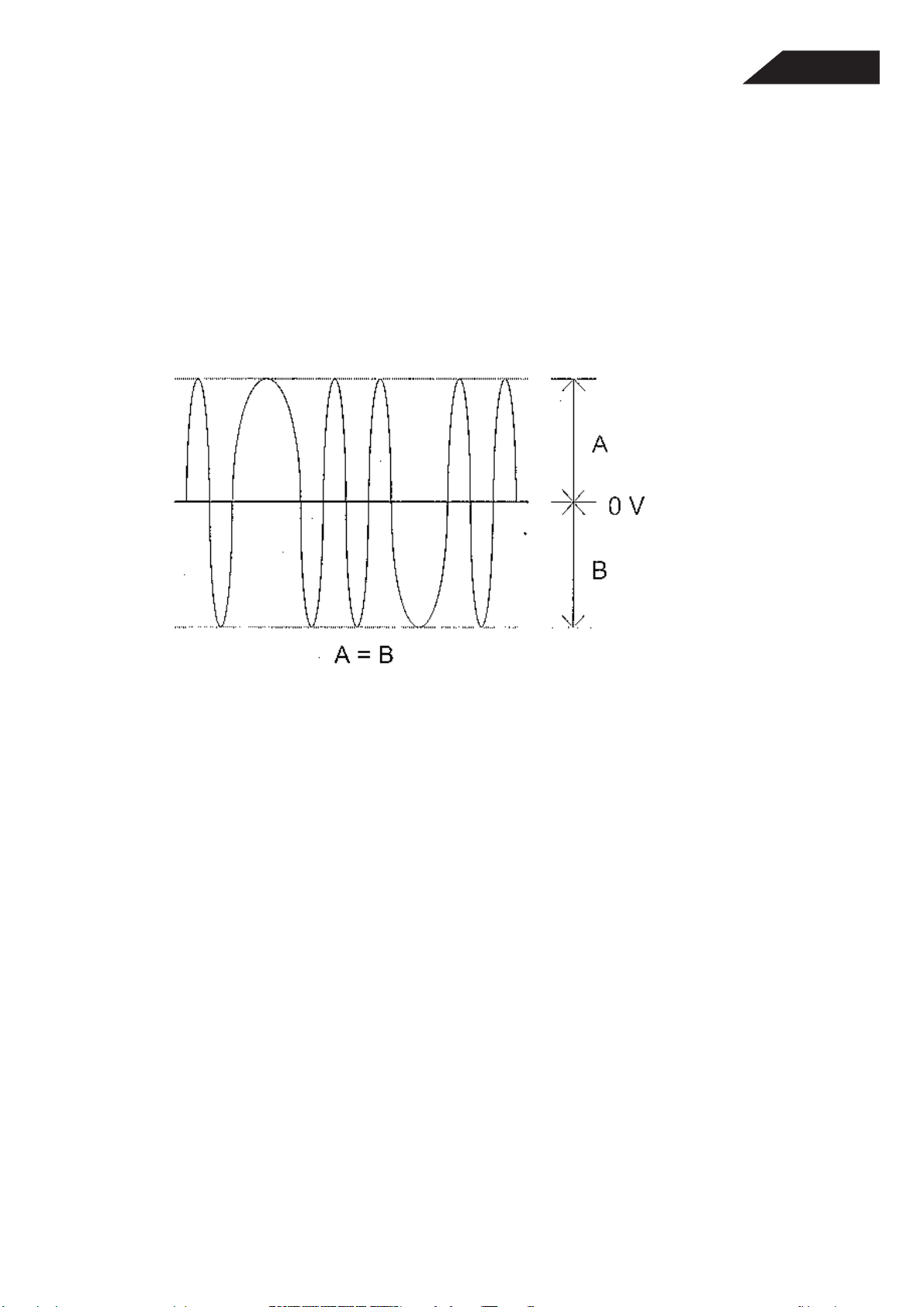
(B) Tracking Adjustment
22
i. Connect oscilloscope to the test point TP3 (KA9220C) and Vref (J6).
ii. Press PLAY button and adjust VR4 to maximum and press SKIP DOWN button to
make it Tracking off.
iii. Adjust VR2 to get symmetrical waveform height. After adjust VR4 to center.
iv. The result is show as below fig. 2
FL8550
Fig. 2
Page 23
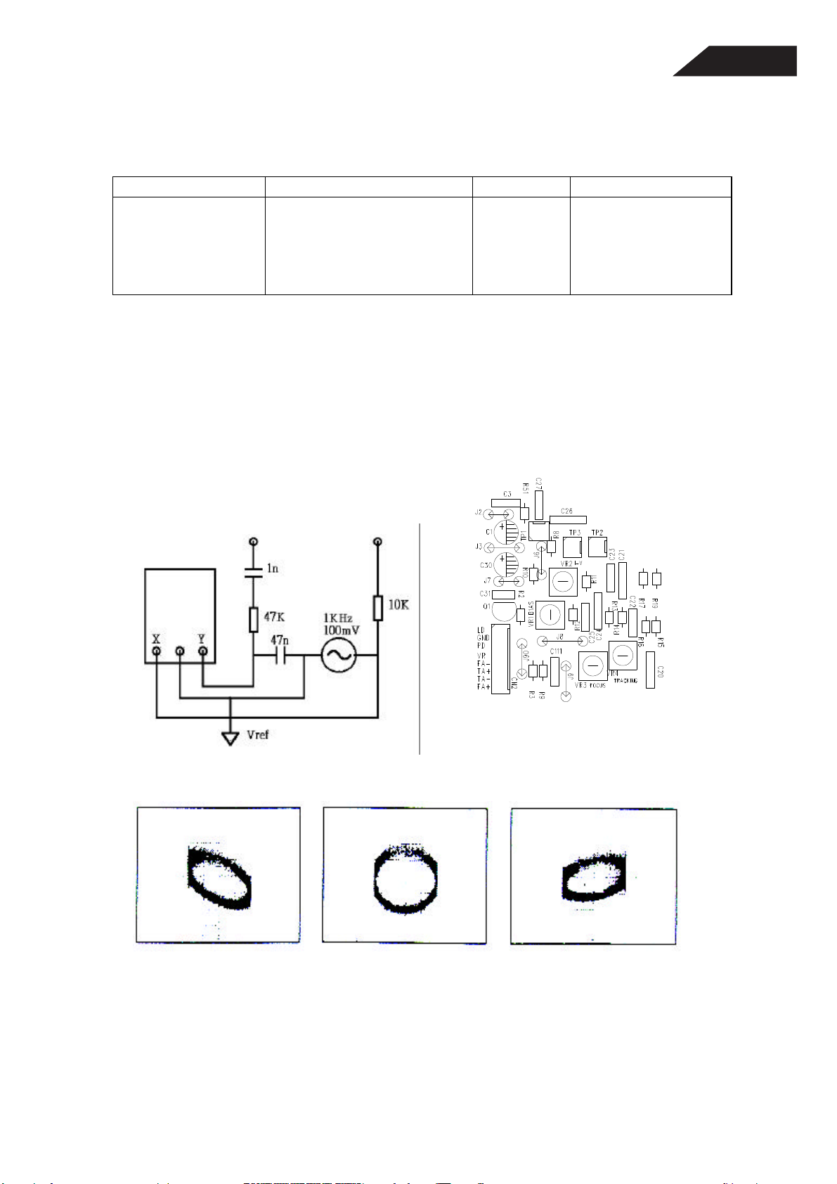
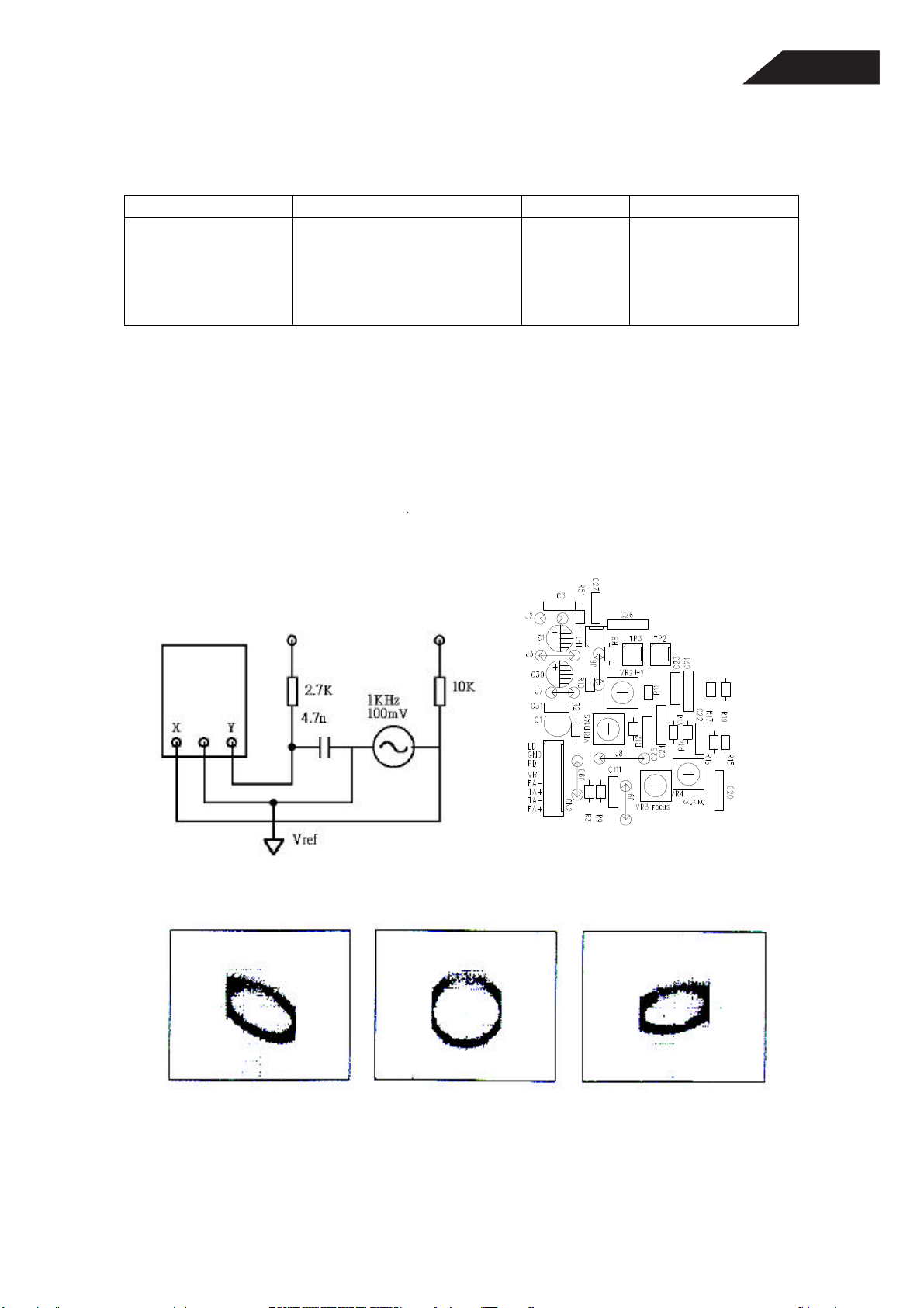
(C) Focus Servo Loop Gain Adjustment
23
Connection point Settings State Adjustment Location
U1 (KA9220C)
Pin 57 (R11)
Pin 56 (R12)
See fig 3
i. Set the frequency generator output to 1KHz and 100mv.
ii. Press the play key and press skip key to move the pickup to halfway across the disk
(R=35mm).
iii. Adjustment VR3(focus gain) so that the Lissajous waveform is symmetrical
above the X axis and the Y axis.
1. Oscilloscope Probe: x 10
2. Oscilloscope setting
CH1: 20mV/division
CH2: 10mV/division
Remark: X-Y mode
Play State Adjustment VR3
FL8550
Focus Gain Adjustment
Fig. 3
Higher gain Optimum gain Lower gain
Page 24
(D) Tracking Servo Loop Gain Adjustment
Vref
24
Connections point Settings State Adjustment location
U1 (KA9220C)
Pin 53 (R13)
Pin 52 (R14)
See fig.4
1. Oscilloscope probe: X10
3. Oscilloscope setting
CH1: 50mV/division
CH2: 20mV/division
Play State Adjustment VR4
Remark: X-Y mode
i. Set the frequency generator output to 1KHz and 100mV.
ii. Press the play key and press skip key to move the pickup to halfway across the disk
(R=35mm).
iii. Adjustment VR4(track gain) so that the Lissajous waveform is symmetrical above
the X axis Y axis.
FL8550
Tracking Gain Adjustment
Fig 4
Higher gain Optimum gain Lower gain
Page 25

Audio Characteristics Test Procedure
25
Test Equipment
1. 3346 CD Player Evaluating Filter x 2 (NF Electronic Instrument)
2. VP7722 Panasonic Audio Analyzer
3. Sony YEDS18 Test CD disc
Procedure
Equipment Setup
1. The audio output of the CD player under test is connected to the CD filter L
& R inputs.
2. The outputs from the filter are connected to the Audio Analyzer.
Check the output Voltage
1. Set the mode of the filter to ‘ THRU’
FL8550
2. Set the mode of Audio Analyzer to ‘ LEVEL’ mode
3. Select track 2 of the test disc and play the CD disc
4. The output voltage and gain of the R & L channels are taken by pressing
the respective buttons on the control board of Audio Analyzer.
Frequency Response
1. Set the mode of the filter to reference level mode.
2. Select the track 3, 4, 5, and 6 of the test disc and run it under ‘ Play’ mode.
3. Check the output of the R & L Channels
Total Harmonic Distortion
1. Set the mode of the filter to ‘ DIST/CH-SP’ mode
2. Set the audio analyzer to ‘ DIST’ mode.
3. Set the unit of the audio analyzer to ‘ %’ mode
4. Select the track 2, 4, and 5 on the test disc and run them under ‘ PLAY’
mode
5. Check the % of each R & L channels
9
Page 26

Signal to Noise Ratio
26
1. Set the mode of the filter to ‘ S/N’ mode
2. Play track 2 of the test disc
3. The unit of the audio analyzer is set to dB mode
4. Press the S/N key on the control panel of the audio analyzer
5. Play track 7
6. Measure the data of S/N ratio
Dynamic Range
1. Set the mode of the filter to ‘ D-Range’ mode
2. Set the audio analyzer to ‘ DIST’ Mode
3. Set the unit of the audio analyzer to ‘ dB’ mode
4. Play track 17of the test disc
5. The dynamic range should be |A| + 60dB
FL8550
Channel Separation
1. Set the mode of the filter to ‘ DIST/CH-SP’ mode
2. Set the audio analyzer to ‘ LEVEL’ mode
3. Play the tracks 8, 9, 10 & 11
4. The measured results is the difference between L & R channel
De-emphasis
1. Press the ‘ THRU’ button of the CD filter
2. Play the track 2 of the test disc
3. Press the ‘ Relative Level’ and make it ‘ ON’
4. Select the track 12 and 13 and measure the L & R channels value
Page 27

FL8550
27
Circuit Description
1. RF AMP BLOCK
The KA9220 is designed for 3-spot type optical pick-up assembly. The photo detector is composed of 6
light sensor (A through F). The photo detector A, B, C and D detect audio modulation signal on the disc
and generate focus error signal.
RF I-V AMP (1) and RF I-V AMP (2) are converted current of PD1 (A + C) and PD2 (B + D) through the
58 Kohm Internal resistor into Voltage.
Furthermore, they are added to RF Summing amplifier.
This signal (A + B + C + D) is outputted from RFO (Pin66).
The output Voltage is as follow.
BA
10K
BA
)
V
) V V ( X2.2 -
) iPD2 iPD1 ( XR3 V
BA
)
RFO
( XR3
V
R1
( 22K X -
10K
V
+−=
V
+−=
R2
+=
+=
Page 28

2. TRACKING ERROR AMPLIFIER
28
FL8550
The output of photo detector F is directed to the (-) Input of F I – V AMP and out of photo detector E is
directed to the (-) input of E I – V AMP.
These input signals are current.
E I – V AMP and F I – V AMP are converted into voltage from the current signal. When correct tracking,
two input (V
AMP output and E I – V AMP output.
=
accordingly,
, VE) signals are equal. The occurrence of tracking error is due to difference between F I – V
F
26K
R
+
=
13K 260K X
A
22K R
1290K X) I - I ( V
FE1TE
=+=
FFF
+++
A
]403K XI 273K )
]260K R 260K
( [ XI V
[ XI V
EE
B
Page 29

FL8550
29
3. FOCUS ERROR AMPLIFIER
The focus error amp is the difference between RF I – V AMP (1) output VA and RF I – V AMP (2) output
V
. This two (VA, VB) signals are each applied to the (-) and (+) input of focus error amp. As the result of
B
differential voltage, Focus error signal is appeared at FE1 Pin (Pin57). This FE1 Output Voltage (low
frequency) becomes (A + C) – (B + D), as follow V
The focus error voltage is directed to the focus servo Block, to maintain optimum focusing at all times.
= R1/R3 (VB – VA)
FE1
4. FOCUS OK GENERATION CIRCUIT
The focus OK circuit generates a timing window to monitor focus search status of focus servo. When
RFO (Pin 66) Voltage is more than –0.37V, the focus OK circuit is inverted. Time constant of HPF in EFM
comparator and in mirror circuit and that of LPF in focus OK circuit are determined bu capacitor (0.01µF)
between RFI and RFO.
Page 30

5. MIRROR CIRCUIT
30
FL8550
After RF input signal is amplified by Mirror amp, it is held in Bottom and Peak hold circuit. Such a hold is
determined by the time constant. Envelope signal A (demodulated to DC) is two-thirds of the peak value
of this signal. The time constant of A signal is held when it is larger than that of B signal. Therefore,
mirror output is; Low at track on disc, High at between tracks on disc, High when defect is detected.
6. DEFECT CIRCUIT
Page 31

FL8550
31
The bottom hold has had two time constant of long and short, after than the RFI signal inverted. The
short time constant of bottom hold is generated shorter than 0.1m sec of disc mirror defect, and long time
constant is generated by previous mirror level. Mirror defect detection signals are generated by
differentiation on Capacitor Coupling, and then transfer level.
7. EFM COMPARATOR
The EFM Comparator converts a RF signal into a binary signal. A processing of disc production is
occurred disproportion because of modification of disc. That is not reduced by only AC coupling. The
reference voltage of EFM comparator is controlled utilizing the fact that the generation-probability 1, 0 is
50% (duty) in the binary EFM signal.
8. APC (AUTOMATIC POWER CONTROL) CIRCUIT
As the Laser diode has had large negative temperature characteristic when it does something for
regularly supply current on laser diode. Therefore, the output on processing monitor photo diode must be
controlled current for getting regularly output power.
Page 32

SERVO BLOCK
32
FL8550
1. FOCUS SERVO
When the defect signal is detected, the focus servo Loop is isolated. At this time, the focus servo error
output is outputted through low pass filter formed by connecting a capacitor (0.1µF) between the built-in
470KΩ resistor and FDFCT Pin (Pin58). Accordingly, the focus error output is held as just before error
value during the defect.
The peak frequency of the focus phase compensation is at about 1.2KHz when the resistor connected to
PFSET(Pin7) is 510KΩ. It is inversely proportional to the resistor connected to the Pin 7.
Page 33

FL8550
33
While the focus search is operating, the FS4 switch is ON and then focus error signal is isolated,
accordingly it is outputted by FSEO Pin (Pin48). When the FS2 switch is ON, the focus servo Loop is on
and then focus error is outputted through the focus servo Loop.
2. TRACKING AND SLED SERVO LOOP
The capacitor across RTG (Pin16) and TGSW (Pin15) reduces high frequency gain when the TG2 switch
is OFF. The Peak frequency of the tracking phase compensation is at about 1.2KHz when the resistor
connected to PFSET (Pin7) is 510KΩ. It is inversely proportional to the resistor connected to the Pin 7.
The tracking error signal is switched into low pass filter route formed by connecting a capacitor between
the built-in resistor at DFCT (470KΩ) and TDFCT (Pin54) as for tracking error signal.
Page 34

3. SPINDLE SERVO AND LOW PASS FILTER
34
FL8550
The 0.033nF and 20KΩ connected to SMEF (Pin 25) form the 200Hz low Pass filter. And the carrier
component of spindle servo error signals is eliminated. In the CLV – S mode, SMEF becomes L and
Pin25 LPF fc lowers, strengthening the filter further.
Page 35

KA9258D
35
4-Channel Motor Driver
FL8550
Features
• 1-phase, full-wave, linear DC motor driver
• Output gain adjustable
• Built in OP-amp
• Built in mute function
• Built in level shift circuit
• Built in thermal shutdown circuit (TSD)
• Operating range 6~13.2V
Description
The KA9258D is a monolithic integrated circuit, suitable for
4-CH motor driver which drives tracking actuator, focus
actuator, sled motor and loading motor of CD/CD-ROM/
DVD system, and can also drive spindle motor of CD
system.
28-SSOPH-375
Typical Applications
• Compact disk player (CDP)
• Video compact disk player (VCD)
• Automotive compact disk player
• Other compact disk media
Ordering Information
Device Package Operating Temp.
KA9258BD 28-SSOPH-375 −40°C ~ +85°C
KA9258BDTF 28-SSOPH-375 −40°C ~ +85°C
Page 36

Pin Definitions
36
Pin Number Pin Name I/O Pin Function Description
1 DO1.1 O Drive output
2 DO1.2 O Drive output
3 DI1.1 I Drive input
4 DI1.2 I Drive input
5 REG - Regulator
6 REO O Regulator output
7MUTEIMute
8 GND1 - Ground 1
9 DI2.1 I Drive input
10 DI2.2 I Drive input
11 DO2.1 O Drive output
12 DO2.2 O Drive output
13 GND2 - Ground 2
14 OPOUT O Op-amp output
15 OPIN(−) I Op-amp input (−)
16 OPIN(+) I Op-amp input (+)
17 DO3.1 O Drive output
18 DO3.2 O Drive output
19 DI3.1 I Drive input
20 DI3.2 I Drive input
21 V
22 V
23 VREF I 2.5V bias voltage
24 DI4.1 I Drive input
25 DI4.2 I Drive input
26 DO4.1 O Drive output
27 DO4.2 O Drive output
28GND3-Ground 3
CC1
CC2
- Supply voltage
- Supply voltage
FL8550
Page 37

Internal Block Diagram
37
GND3
DO4.2
DO4.1
+
−
Level
shift
−
+
+
−
Level
shift
−
12 345 6 8 9 10 11 12 13714
10k
+
10k
10k
FL8550
OPIN (−)
DI4.2
DI4.1
VREF
10k
TSD
Regulator
−
+
10k
VCC2
10k
+
Mute
50k
−
50k
VCC1
DI3.2
DI3.1
DO3.2
DO3.1
10k
+
−
Level
10k
10k
10k
shift
−
+
−
+
Level
shift
+
−
OPIN(+)
1516171819202122232425262728
+
−
DO1.1
DO1.2
Pin Assignments
GND3
DO4.2
1234567 891011121314
DO1.1
DO1.2
REG
DI1.1
DI1.2
DO4.2
DI4.2
REO
MUTE
FIN
(GND)
DI4.1
CC2
VREF
V
GND1
CC1
V
DI2.1
DI2.2
DO2.1
DI3.2
DI3.1
GND2
DO2.2
DO3.2
OPOUT
)
−
DO3.1
OPIN (+)
OPIN (
1516171819202122232425262728
KA9258D
REG
DI1.1
DI1.2
REO
MUTE
FIN
(GND)
GND1
DI2.1
DI2.2
DO2.1
GND2
DO2.2
OPOUT
Page 38

KA9220C
38
FL8550
Page 39

FL8550
39
Page 40

FL8550
40
Page 41

FL8550
41
Page 42

FL8550
42
Page 43

FL8550
43
Page 44

KS9284
44
FL8550
Page 45

FL8550
45
Page 46

FL8550
46
Page 47

FL8550
47
Page 48

FL8550
48
Page 49

FL8550
49
Page 50

KA8301
50
Bi-Directional DC Motor Driver
FL8550
Features
• Built-in brake function.
• Built-in element to absorb a surge current derived from
changing motor direction and braking motor drive.
• External motor speed control pin
• Motor direction change circuit.
• Interfaces with CMOS devices.
Description
The KA8301 is a monolithic integrated circuit designed for
driving bi-directional DC motor with braking and speed control, and it is suitable for the loading motor driver of VCR
systems. The speed control can be achieved by adjusting the
external voltage of the speed control pin.
10-SIPH-B
Typical Application
• Video cassette recorder (VCR) loading motor
• Low current DC motor such audio or video equipment
• General DC motor
Ordering Information
Device Package Operating Temp.
KA8301-L 10-SIPH-B −25°C ~ +75°C
Page 51

Pin Assignments
51
FL8550
KA8301
GND V
OUT1VZ1
12345678910
V
F
R
R
IN
V
IN
CC1
V
CC2VZ2
Pin Definitions
Pin Number Pin Name I/O Pin Function Description
1 GND - Ground
2V
3V
4V
5F
6R
7V
8V
9V
10 V
OUT1
Z1
R
IN
IN
CC1
CC2
Z2
OUT2
O Output 1
- Phase compensation
I Motor speed control
I Input 1
I Input 2
- Supply voltage (Signal)
I Supply voltage (Power)
I Phase compensation
O Output 2
V
OUT2
Page 52

FL8550
52
®
49%
PCM1702P
FPO
PCM1702U
BiCMOS Advanced Sign Magnitude 20-Bit
DIGITAL-TO-ANALOG CONVERTER
DESCRIPTIONFEATURES
● ULTRA LOW –96dB max THD+N
(No External Adjustment Required)
● NEAR-IDEAL LOW LEVEL OPERATION
● GLITCH-FREE OUTPUT
● 120dB SNR TYP (A-Weight Method)
● INDUSTRY STD SERIAL INPUT FORMAT
● FAST (200ns) CURRENT OUTPUT
±1.2mA)
(
● CAPABLE OF 16X OVERSAMPLING
● COMPLETE WITH REFERENCE
● LOW POWER (150mW typ)
The PCM1702 is a precision 20-bit digital-to-analog
converter with ultra-low distortion (–96dB typ with a
full scale output). Incorporated into the PCM1702 is
an advanced sign magnitude architecture that eliminates unwanted glitches and other nonlinearities around
bipolar zero. The PCM1702 also features a very low
noise (120dB typ SNR: A-weighted method) and fast
settling current output (200ns typ, 1.2mA step) which
is capable of 16X oversampling rates.
Applications include very low distortion frequency
synthesis and high-end consumer and professional
digital audio applications.
Clock
Data
LE
DCOM
ACOM
+V
CC
–V
CC
International Airport Industrial Park • Mailing Address: PO Box 11400 • Tucson, AZ 85734 • Street Address: 6730 S. Tucson Blvd. • Tucson, AZ 85706
Tel: (520) 746-1111 • Twx: 910-952-1111 • Cable: BBRCORP • Telex: 066-6491 • FAX: (520) 889-1510 • Immediate Product Info: (800) 548-6132
© 1993 Burr-Brown Corporation PDS-1175B Printed in U.S.A. June, 1995
Input Shift Register
and Control Logic
Reference
and
Servo
SERV DCRF DC
Balanced Current
Segment DAC A
Balanced Current
Segment DAC B
Bipolar Offset
BPO DC
1
I
OUT
PCM1702
®
Page 53

FL8550
53
SPECIFICATIONS
All specifications at 25°C, ±VCC and +V
PARAMETER CONDITIONS MIN TYP MAX UNITS
RESOLUTION 20 Bits
DYNAMIC RANGE, THD + N at –60dB Referred to Full Scale, with A-weight 110 dB
DIGITAL INPUT
Logic Family TTL/CMOS Compatible
Logic Level: V
Data Format Serial, MSB First, BTC
IH
V
IL
I
IH
I
IL
Input Clock Frequency 12.5 20.0 MHz
TOTAL HARMONIC DISTORTION + N
P/U VO = 0dB fS = 352.8kHz
V
= –20dB fS = 352.8kHz
O
V
= –60dB fS = 352.8kHz
P/U, -J V
P/U, -K V
O
= 0dB fS = 352.8kHz
O
V
= –20dB fS = 352.8kHz
O
V
= –60dB fS = 352.8kHz
O
= 0dB fS = 352.8kHz
O
V
= –20dB fS = 352.8kHz
O
V
= –60dB fS = 352.8kHz
O
ACCURACY
Level Linearity At –90dB Signal Level ±0.5 dB
Gain Error ±0.5 ±3%
Bipolar Zero Error
(5)
Gain Drift 0°C to 70°C ±25 ppm of FSR/°C
Bipolar Zero Drift 0°C to 70°C ±5 ppm of FSR/°C
Warm-up Time 1 minute
IDLE CHANNEL SNR
(6)
ANALOG OUTPUT
Output Range ±1.2 mA
Output Impedance 1.0 kΩ
Settling Time (±0.003% of FSR, 1.2mA Step) 200 ns
Glitch Energy No Glitch Around Zero
POWER SUPPLY REQUIREMENTS
Supply Voltage Range: +V
Combined Supply Current: +I
Combined Supply Current: –I
Power Dissipation ±V
= +V
CC
–V
= –V
CC
CC
CC
TEMPERATURE RANGE
Operating –25 +85 °C
Storage –55 +125 °C
NOTES: (1) Binary Two’s Complement coding. (2) Ratio of (Distortion
(4) D/A converter output frequency (signal level). (5) Offset error at bipolar zero. (6) Measured using an OPA627 and 5kΩ feedback and an A-weighted filter.
= ±5V unless otherwise noted.
DD
(2)
DD
DD
PCM1702P/U, -J, -K
+2.4 +V
0 0.8 V
VIH = +V
DD
VIL = 0V ±10 µA
(3)
, f = 1002Hz
(3)
, f = 1002Hz
(3)
, f = 1002Hz
(3)
, f = 1002Hz
(3)
, f = 1002Hz
(3)
, f = 1002Hz
(3)
, f = 1002Hz
(3)
, f = 1002Hz
(3)
, f = 1002Hz
(4)
(4)
(4)
(4)
(4)
(4)
(4)
(4)
(4)
–92 –88 dB
–82 –74 dB
–46 –40 dB
–96 –92 dB
–83 –76 dB
–48 –42 dB
–100 –96 dB
–84 –80 dB
–50 –44 dB
DD
±10 µA
(1)
±0.25 %
Bipolar Zero, A-weighted Filter 110 120 dB
+4.75 +5.00 +5.25 V
–4.75 –5.00 –5.25 V
+VCC = +VDD = +5V +5.00 +9.0 mA
–V
= –V
= –5V –25.00 –41.0 mA
CC
DD
= ±VDD = ±5V 150 250 mW
CC
RMS
+ Noise
) / Signal
RMS
. (3) D/A converter sample frequency (8 x 44.1kHz; 8x oversampling).
RMS
V
The information provided herein is believed to be reliable; however, BURR-BROWN assumes no responsibility for inaccuracies or omissions. BURR-BROWN assumes
no responsibility for the use of this information, and all use of such information shall be entirely at the user’s own risk. Prices and specifications are subject to change
without notice. No patent rights or licenses to any of the circuits described herein are implied or granted to any third party. BURR-BROWN does not authorize or warrant
any BURR-BROWN product for use in life support devices and/or systems.
®
PCM1702
Page 54

FL8550
54
ABSOLUTE MAXIMUM RATINGS (DIP Package)
Power Supply Voltage .................................................................. ±6.5VDC
Input Logic Voltage ........................................... DGND—0.3V~+V
Operating Temperature..................................................... –25 °C to +85°C
DD
+0.3V
Storage Temperature ...................................................... –55°C to +125°C
Power Dissipation ..........................................................................500mW
Lead Temperature (soldering, 10s).................................................. 260°C
PIN ASSIGNMENTS (DIP Package)
PIN MNEMONIC PIN MNEMONIC
1 DATA 9 +V
2 CLOCK 10 BPO DC
3+V
4 DCOM 12 ACOM
5–V
6 LE 14 SERV DC
DD
DD
11 I
13 ACOM
7 NC 15 REF DC
8NC16–V
PACKAGE INFORMATION
(1)
PACKAGE DRAWING
MODEL PACKAGE NUMBER
PCM1702P 16-Pin Plastic DIP 180
PCM1702U 20-Pin Plastic SOP 248
NOTE: (1) For detailed drawing and dimension table, please see end of data
sheet, or Appendix D of Burr-Brown IC Data Book.
CC
OUT
CC
ABSOLUTE MAXIMUM RATINGS (SOP Package)
Power Supply Voltage .................................................................. ±6.5VDC
Input Logic Voltage ........................................... DGND—0.3V~+V
Operating Temperature..................................................... –25°C to +85°C
DD
+0.3V
Storage Temperature ...................................................... –55°C to +125°C
Power Dissipation ..........................................................................300mW
Lead Temperature (soldering, 5s).................................................... 260°C
PIN ASSIGNMENTS (SOP Package)
PIN MNEMONIC PIN MNEMONIC
1 DATA 11 +V
2 CLOCK 12 BPO DC
CC
3NC13NC
4+V
5 DCOM 15 ACOM
6–V
7 LE 17 SERV DC
DD
DD
14 I
OUT
16 ACOM
8NC18NC
9 NC 19 RFE DC
10 NC 20 –V
CC
GRADE MARKING (SOP Package)
MODEL PACKAGE
PCM1702U Marked PCM1702.
PCM1702U-J Marked with white dot by pin 10.
PCM1702U-K Marked with red dot by pin 10.
CONNECTION DIAGRAM
CLOCK
DATA
LE
+5V V
DD
47µF
47µF
–5V V
DD
+
+
= SOP
= DIP
47µF
+
47µF
+
–5V V
CC
R
NF
V
OUT
2
2
1
1
6
7
3
4
4
5
5
6
16
20
15
19
14
17
11
14
10
12
9
11
13
16
12
15
22µF
+
+
47µF
+
+5V V
100µF
CC
®
PCM1702
Page 55

FL8550
55
®
PMD-100
PMD-100 Process Decoder
General Description
The PMD-100 HDCD® Process Decoder is a sophisticated
0.6 micron CMOS Integrated Circuit that performs precise decoding of HDCD encoded recordings. The D ecoder
also functions as a state-of-the-art digital filter when fed
data from non-HDCD recordings. It is designed to interface directly with popular data receivers and DAC’s, eliminates the need for conventional monolithic digital filters.
The PMD-100 has been carefully designed to maximize performance and ease of use in a wide variety of applications.
HDCD Process Information
Data encoded with HDCD process information carries precisely encrypted signals, hidden within the LSB of the 16bit data word. Over time, only 1 to 5% of the LSB is used
for this hidden code. The encoded information is inaudible and causes no perceptible loss of information. The
PMD-100 recognizes the encrypted signals as HDCD process information, and directs the decoding function to precisely reconstruct the high resolution signal in a form appropriate for output to the D-A converter being used.
Note: To preserve HDCD process information, no alteration
of the encoded data is allowed prior to processing by the PMD-
100. Digital data processing including phase inversion prior to
the PMD-100 input will result in the loss of HDCD process
information encoded in the data.
SPECIAL FEATURES
Automatic HDCD Process Decoding
When the PMD-100 detects HDCD® process information in the input data, it automatically switches to
®
HDCD
an LED indicator. When non-HDCD
data is received, the decoder automatically operates
as a high performance digital filter.
Excellent Filter Characteristics
When operating as a digital filter, the PMD-100 exhibits passband characteristics that have been carefully optimized to provide extremely accurate sound
quality. Passband ripple from 0 to 20 kHz is within
±.0001 dB and stopband attenuation is greater than
120 dB.
Two Operating Modes
Stand-Alone
In Stand-Alone Mode, the PMD-100 requires no
external controller, allowing for the most cost
effective designs.
Program
In Program mode, an external processor controls
the PMD-100’s many advanced operating modes
and features.
decode mode, and provides an output to drive
®
process input
9300-0005
Rev A1
HDCD
HDCD® and High Definition Compatible Digital®
are registered trademarks of Pacific Microsonics, Inc
Page 56

PMD-100
56
PMD-100 Process Decoder
FL8550
®
SPECIAL FEATURES (Cont.)
DAC Optimize Operating Modes
To achieve the best possible performance from a variety of
different DAC types, adjustable parameters are provided including eight different levels of dither and Patented “Silent
Conversion” variable clock timing.
Constant Clock Output
The PMD-100 constantly provides output clocking to the DAC,
even if input data and master clocks are lost. This feature eliminates the possiblility of spikes or DC offsets at the DAC’s output.
Additional Features
•
24 bit or greater accuracy provided for all opera-
tions.
•
Up to 24 bit input data passed without truncation.
•
32 kHz to 55 kHz input data rates.
•
Output digital attenuation over a 96 dB range in
0.188 dB steps.
•
Output soft mute and hard mute functions.
•
16, 18, 20 or 24 bit output data.
•
8 Fs, 4 Fs or 2 Fs output data rates. (Multiple
output data rates are provided to allow flexible DAC
operation and ease of use in designs that employ
custom DSP based filters for non-HDCD
recordings.)
•
Digital domain deemphasis.
•
256 Fs or 384 Fs system clock.
®
process
Digital Characterisitcs
= 4.75V to 5.25V, VSS = OV, TA = 0°C to +70°C unless otherwise specified.
V
DD
Page 57

PMD-100
57
PMD-100 Process Decoder
Pin Description (Stand-Alone Mode) Pin 9 Low
( I = Input, O = Output. All input levels TTL compatible
except XTI which must be CMOS level. No inputs have
pull-ups. All outputs are full CMOS levels. )
1: DIN (I) Serial data input.
2: BCKI (I) Bit clock input.
3: XTIM(I) Select system clock frequency.
Low = 256 Fs, High = 384 Fs.
4: DITH(I) Dither select.
Low = dither disabled,
High = dither added.
5: GAIN (O) Analog output stage gain.
Use only if Pin 19 is High (see page
14).
Low = low gain,
High = high gain (+6 dB).
(See pin 19 description).
6: XTI (I) System clock input.
7: VDD1 +5 volt power for filter.
8: VSS1 Ground
9: PROG(I) Select Program mode.
Low = Stand-Alone,
High = Program.
Note: Pins 10 through 14 perform different functions
depending on whether Stand-Alone or Program mode is
selected.
Stand-Alone Mode:
10: OSIZ0 (I)
11: OSIZ1 (I)
These two pins determine the output word size, as well as
the number of pulses on BCKO.
12: COB (I) Output data format.
Low = complementary offset binary,
High = 2’s complement.
13: JUST (I) Input data justification.
Low = data assumed to be left justi
fied up to 24 bits in length,
High = data right justified 16 bits.
14: BCPL (I) Input data latching.
Low = input data latched on rising
edge of BCKI. High = input data
latched on falling edge of BCKI.
15: SMUTE (I) Soft mute. Low = off, High = on.
16: DEEMPH(I)De-emphasis filter.
FL8550
®
Low = off, High = on.
17: HMUTE (I) Hard mute. Low = off, High = on.
18: FSEL (I) De-emphasis filter Fs.
Low = 44.1 kHz, High = 48 kHz.
19: SCAL (I) Gain scaling.
Low = 6dB gain scaling is performed
internally in the digital domain,
High = analog output gain stage is set
by pin 5 GAIN. (See page 14.)
20: DG (O) DAC sample and hold deglitch signal.
21: VSS2 Ground. (Common with VSS1)
22: VDD2 +5 volt power for output interface.
23: DOR (O) Right channel serial data output.
24: DOL (O) Left channel serial data output.
25: WCKO(O) Word clock output.
26: BCKO (O) Bit clock output.
27: HDCD (O) HDCD encoding detect.
Low = no encoding. High = HDCD
encoded input data. (Output current
rated at 12mA.)
28: LRCI (I) Word clock input.
Page 58

HD6433724E93F MICROPROCESSOR
58
Overview
The H8/300L Series is a single-chip microcomputer (MCU: microcomputer unit),
built around the high-speed H8/300L CPU and equipped with peripheral system
functions on chip.
The H8/3724 and H8/3754 Series are single-chip microcomputers in the H8/300L
Series equipped with high-voltage pins. Their on-chip peripheral functions include a
vacuum fluorescent display (VFD) controller/driver, timers, a 14-bit PWM (pulse
width modulator), two serial communication interface channels, and an analog-todigital converter. Together these functions make this chip ideally suited to use as a
microcontroller in embedded systems requiring a VFD display.
The H8/3724 and H8/3754 Series come in the following memory configurations for
FL8550
various system scale needs.
H8/3723: 24-kbyte ROM, 384-byte RAM
H8/3724: 32-kbyte ROM, 512-byte RAM
H8/3725: 40-kbyte ROM, 640-byte RAM
H8/3726: 48-kbyte ROM, 1,024-byte RAM
H8/3753: 24-kbyte ROM, 1,024-byte RAM
H8/3754: 32-kbyte ROM, 1,024-byte RAM
In addition to masked ROM versions available for the H8/3724 Series, H8/3724 and
H8/3726 are also available in ZTATTM versions which allow the user to freely
program the on-chip PROM.
Note: * ZTAT (zero turn around time) is a trademark of Hitachi, Ltd.
Page 59

Internal Block Diagram
59
FL8550
Page 60

Pin Arrangement
60
FL8550
Page 61

REF. NO. PART NO. DESCRIPTION QTY.
61
FL8550 MAIN BOARD
RESISTOR
R32/33/35-37/52/5963/79/80.
R1/11/13/27/48/49/50. 1001-002316-000 CARBON FILM RESISTOR 1K OHM 1/6W ±5% 7
R20/21/26/42/110. 1001-003316-000 CARBON FILM RESISTOR 10K OHM 1/6W ±5% 5
R5/15/18/24/25. 1001-004316-000 CARBON FILM RESISTOR 100K OHM 1/6W ±5% 5
R7/64. 1001-005316-000 CARBON FILM RESISTOR 1M OHM 1/6W ±5% 2
R111. 1001-501312-000 CARBON FILM RESISTOR 150 OHM 1/2W ±5% 1
R14/22. 1001-504316-000 CARBON FILM RESISTOR 150K OHM 1/6W ±5% 2
R9/10. 1001-803316-000 CARBON FILM RESISTOR 18K OHM 1/6W ±5% 2
R6. 1001-804316-000 CARBON FILM RESISTOR 180K OHM 1/6W ±5% 1
J101. 1002-200312-000 CARBON FILM RESISTOR 22 OHM 1/2W ±5% 1
R2. 1002-200316-000 CARBON FILM RESISTOR 22 OHM 1/6W ±5% 1
R44. 1002-201316-000 CARBON FILM RESISTOR 220 OHM 1/6W ±5% 1
R34. 1002-202316-000 CARBON FILM RESISTOR 2.2K OHM 1/6W ±5% 1
R8/12. 1002-203316-000 CARBON FILM RESISTOR 22K OHM 1/6W ±5% 2
R38. 1002-701316-000 CARBON FILM RESISTOR 270 OHM 1/6W ±5% 1
R29/51/84. 1002-703316-000 CARBON FILM RESISTOR 27K OHM 1/6W ±5% 3
R30/31/39/40/41. 1003-302316-000 CARBON FILM RESISTOR 3.3K OHM 1/6W ±5% 5
R16/45/85. 1003-303316-000 CARBON FILM RESISTOR 33K OHM 1/6W ±5% 3
R3. 1004-700316-000 CARBON FILM RESISTOR 47 OHM 1/6W ±5% 1
R46. 1004-701316-000 CARBON FILM RESISTOR 470 OHM 1/6W ±5% 1
R53-57/109. 1004-702316-000 CARBON FILM RESISTOR 4.7K OHM 1/6W ±5% 6
R4. 1005-104316-000 CARBON FILM RESISTOR 510K OHM 1/6W ±5% 1
R23. 1005-602316-000 CARBON FILM RESISTOR 5.6K OHM 1/6W ±5% 1
R19. 1005-603316-000 CARBON FILM RESISTOR 56K OHM 1/6W ±5% 1
R58. 1006-801316-000 CARBON FILM RESISTOR 680 OHM 1/6W ±5% 1
R17. 1006-803316-000 CARBON FILM RESISTOR 68K OHM 1/6W ±5% 1
R83. 1008-200316-000 CARBON FILM RESISTOR 82 OHM 1/6W ±5% 1
R28. 1008-202316-000 CARBON FILM RESISTOR 8.2K OHM 1/6W ±5% 1
R47. 1009-100316-000 CARBON FILM RESISTOR 91 OHM 1/6W ±5% 1
R105-108. 1011-002014-000 METAL FILM RESISTOR 1K OHM 1/4W ±1% 4
R77/78. 1011-104016-000 METAL FILM RESISTOR 100K 1/6W ±1% 2
R71-76 1011-502016-000 METAL FILM RESISTOR 1.5K OHM 1/4W ±1% 6
R67/68 1011-802014-000 METAL FILM RESISTOR 1.8K OHM 1/4W ±1% 2
R69/70 1014-701014-000 METAL FILM RESISTOR 470K OHM 1/4W ±1% 2
R65/66 1015-102016-000 METAL FILM RESISTOR 5.1K OHM 1/6W ±1% 2
VR1 1051-003500-001 VARIABLE RESISTOR 10K OHM ±30% 1
VR2-4 1052-003600-110 VARIABLE RESISTOR 20K OHM ±30% 3
CAPACITOR
C50/51 1100-100042-001 CERAMIC CAP. 10pF/50V ±5% NPO 2
C44/114/122 1100-102044-000 CERAMIC CAP. 1000pF/50V ±20% 3
C97/98/104108/121/128
C38/45-47/49/7780/85/86/91-94/99/111
C67/68 1100-221043-000 CERAMIC CAP. 220pF/50V ±10% 2
C31 1101-102063-000 POLYESTER/MYLAR CAP. 0.001uF/100V ±10% 1
C6/12/18/27/32 1101-103063-000 POLYESTER/MYLAR CAP. 0.01uF/100V ±10% 5
C8/9/16/19/20/24/26 1101-104063-000 POLYESTER/MYLAR CAP. 0.1uF/100V ±10% 7
C37 1101-152063-000 POLYESTER/MYLAR CAP. 0.0015uF/100V ±10% 1
C3/4/23/34/35 1101-223063-000 POLYESTER/MYLAR CAP. 0.022uF/100V ±10% 5
C5 1101-332063-000 POLYESTER/MYLAR CAP. 3300pF/100V ±10% 1
C7/13/29 1101-333063-000 POLYESTER/MYLAR CAP.0.033uF/100V ±10% 3
C21/25/36 1101-473063-000 POLYESTER/MYLAR CAP. 0.047uF/100V ±10% 3
C22 1101-682063-000 POLYESTER/MYLAR CAP. 0.0068uF/100V ±10% 1
C1/2/30/33/102/103 1102-101014-000 ELECT. CAP. 100uF/16V ±20% 6
C61-66 1102-101024-000 ELECT. CAP. 100uF/25V ±20% 6
C17 1102-220014-000 ELECT. CAP. 22uF/16V ±20% 1
1001-001316-000 CARBON FILM RESISTOR 100 OHM 1/6W ±5% 13
1100-103044-000 CREAMIC CAP. 0.01uF/50V ±20% 9
1100-104044-000 CERAMIC CAP. 0.1uF/50V ±20% 17
1101-222062-000 POLYESTER/ MYLAR CAP. 2200pF/100V ±5% 6
FL8550
Page 62

C39/-39/42/75/76/100 1102-221014-000 ELECT. CAP. 220uF/16V ±20% 6
62
C95/96/101 1102-222014-000 ELECT. CAP. 2200uF/16V ±20% 3
C53-60 1102-337024-000 ELECT. CAP. 3.3uF/25V ±20% 8
C11/28/43 1102-470014-000 ELECT. CAP. 47uF/16V ±20% 3
C41/48/87-90 1102-471014-000 ELECT. CAP. 470uF/16V ±20% 6
C10 1102-477044-000 ELECT. CAP. 4.7uF/50V ±20% 1
C14/15 1102-478044-000 ELECT. CAP. 0.47UF/50V ±20% 2
TRANSISTOR
Q4/6/7 1300-805000-100 TRANSISTOR NPN 8050D TO92 (SAMSUNG) 3
Q5 1300-945000-100 TRANSISTOR NPN KSC945-Y (SAMSUNG) 1
Q1 1301-733000-100 TRANSISTOR PNP A733 1
Q2 1301-928000-100 TRANSISTOR PNP KS928A TO-92 (SAMSUNG) 1
DIODE
D1-5/7-10 1401-140020-000 DIODE RECTIFIER 1N4002 9
D6/11 1401-141480-000 DIODE 1N4148 2
ZD3 1402-510001-200 ZENER DIODE 5.1V 1/2W 1
ZD2 1402-560000-000 ZENER DIODE 5.6V 1/2W 1
ZD1 1402-620001-200 ZENER DIODE 6.2V1/2W 1
MISCELLANEOUS
J20 1503-353400-100 FERRITE COILS B3534 1
XTAL 1600-169343-000 CRYSTAL 16.9344 ± 30PPM 49U3H TYPE 1
CN19 2300-002000-001 STRAIGHT CONN. WAFER 2PINS 2mmP JST 1
CN20 2300-003000-001 STRAIGHT CONN. WAFER 3PINS 2mmP JST 1
CN1 2300-005000-000 STRAIGHT CONN. WAFER 5PINS 2mmP 1
CN3/5/6/17/18 2300-006000-001 STRAIGHT CONN. WAFER 6PINS 2mmP JST 5
CN2 2300-008000-000 STRAIGHT CONN. WAFER 8PINS 2mmP 1
CN11 2300-010000-000 STRAIGHT CONN. WAFER 10PINS 2mmP 1
CN10 2300-012000-000 STRAIGHT CONN. WAFER 12PINS 2mmP 1
CN4/14 2500-023001-040 2PINS 300MM 1CONN.(JST) CABLE AWG#26 2mmP 2
CN21 TO CN502 2500-037001-050 3PINS 700MM 1CONN. CABLE AWG#28 2mmP 1
CN3 2501-062801-150 6PINS 280MM 2CONN. RIBBON CABLE AWG#28 2mmP 1
CN2 2501-084001-150 8PINS 400MM 2CONN. CABLE AWG#28 2mmP 1
CN5 TO CN17 2506-062201-150 6PINS 220MM 2CONN. RIBBON CABLE AWG#28 2mmP 1
CN13 TO CN713 2510-024501-050 2PINS 450MM 1CONN. SHIELD CABLE AWG#28 2mmP 1
CN15 TO CN712 2510-044501-050 4PINS 450MM 1CONN. SHIELD CABLE AWG#28 2mmP 1
CN16 2510-047001-050 4PINS 700MM 1CONN. SHIELD CABLE AWG#28 2mmP 1
CN1 2510-052501-060
2600-100654-200 65MM JUMPER WIRE AWG#26 UL1007 RED 1
2600-102004-000 200MM JUMPER WIRE AWG#26 UL1007 BLACK 1
4002-311975-000 TOROID COILS “T31X19X7.5MM” 2
F101 4030-100000-000 MICRO FUSE 1A 1
RLY 1/2 4050-520000-000 RELAY DS2Y-SDC5V (NATIONAL) 2
5PINS 250MM 1 CONN. SHIELD CABLE AWG#30 2mmP 1
INTEGRATED CIRCUIT
U9 4100-100056-200 I.C. PMD100 HDCD DIP (PACIFIC MICROSONICS)
HDCD DECODER
U10/11 4117-020104-600 I.C. PCM1702U SOP (BURR-BROWN) DAC 2
U12-15 4155-320052-100 I.C. NE5532N 8P DIP (PHILIPS) OP-AMP 4
U8 4174-040012-100 I.C. 74HC04 DIP (PHILIPS) CMOS 1
U7 4174-740052-100 I.C. 74HC74 DIP (PHILIPS) CMOS 1
U16 4178-050304-100 I.C. 7805 3PINS TO-220 (JRC) REGULATOR 1
U19 4178-050310-000 I.C. LM78L05 TO92 REGULATOR 1
U6 4178-080301-400 I.C. MC7808AC 3PINS TO-220 (MOTOROLA)
REGULATOR
U17 4178-080310-000 I.C. 78L08 TO92 (MIRCO) REGULATOR 1
U20 4179-050310-000 I.C. LM79L05 TO92 REGULATOR 1
U18 4179-080311-600 I.C. 79L08 TO92 (NJRC) OP-AMP 1
U4/5 4183-010020-400 I.C. KA8301 10PINS SIL MOTOR DRIVER 2
U1 4192-200122-400 I.C. KA9220C QFP SAMSUNG SSP 1
U2 4192-580122-400 I.C. KA9258D SMT SAMSUNG MOTOR DRIVE 1
U3 4192-840122-400 I.C. KS9284 QFP SAMSUNG DSP 1
FL8550
1
1
Page 63

FL8350/8550 HEADPHONE BOARD
63
RESISTOR
R511-514 1001-003316-000 CARBON FILM RESISTOR 10K OHM 1/6W +-5% 4
R507-510 1001-004316-000 CARBON FILM RESISTOR 100K OHM 1/6W +-5% 4
R503/504 1001-503316-000 CARBON FILM RESISTOR 15K OHM 1/6W +-5% 2
R501/502 1004-701316-000 CARBON FILM RESISTOR 470 OHM 1/6W +-5% 2
R515/516 1005-600314-000 CARBON FILM RESISTOR 56 OHM 1/6W +-5% 2
R505 1065-003500-130 VAR. RESISTOR 50K 1/4W +-20% ROTARY B-TYPE 1
CAPACITOR
C509/510 1100-102044-000 CERAMIC CAP. 1000pF/50V +-20% 2
C511 1100-103044-000 CERAMIC CAP. 0.01uF/50V +-20% 1
C503/504/511 1100-104044-000 CERAMIC CAP. 0.1uF/50V +-20% 3
C505-508 1102-100044-000 ELECT. CAP. 10uF/50V +-20% 4
C501/502 1102-101044-000 ELECT. CAP. 100uF/50V +-20% 2
MISCELLANEOUS
CN501-502 2300-003000-001 STRAIGHT CONN. WAFER 3PINS 2mmP JST 2
U502 2320-009911-003 6.4MM HEADPHONE JACK (JY-6303-02-030) GD
PLT
2605-100902-000 90MM GND WIRE 1RING (M3) AWG#22 BLK 1
INTEGRATED CIRCUIT
U501 4145-580051-600 I.C. NJM 4558L (NJRC) OP-AMP 1
FL8550
1
FL8350/8550 CONTROL BOARD
RESISTOR
R831-832 1001-201316-000 CARBON FILM RESISTOR 120 OHM 1/6W +-5% 2
R833 1001-801316-000 CARBON FILM RESISTOR 180 OHM 1/6W +-5% 2
R834 1001-201316-000 CARBON FILM RESISTOR 120 OHM 1/6W +-5% 1
R835 1002-201316-000 CARBON FILM RESISTOR 330 OHM 1/6W +-5% 1
MISCELLANEOUS
S831-835 2400-020200-000 TACT SW 2P2T KPT-1105A (5MM) 5
CN831 2500-022001-040 2PIN 200MM 1 CONN CABLE AWG#26 2MMP 1
FL8350/8550 POWER BOARD
2610-221000-000 2100MM POWER CORD W/POLARZED PLUG UL
SPT-2 AWG#18
3200-480140-401 TRANSFORMER EI48 118V CUL #4801Y44T-1
(WINBOND)
4002-311975-000 TOROID COILS “T31X19X7.5MM” 1
FL8350/8550 POWER CONTROL BOARD
RESISTOR
R841 1001-501316-000 CARBON FILM RESISTOR 150 OHM 1/6W ±5% 1
MISCELLANEOUS
S841 2400-020200-003 PUSH SWITCH 2P2T ESB64801 (MATSUSHITA) 1
CN841 2500-032201-050 3PIN 220MM 1CONN CABLE AWG#28 UL1571 1
D841 3100-204000-001 LED 5MM BI-COLOR A/G #BL-BAG204 1
1
1
FL8550 MCU BOARD
RESISTOR
R701 1001-000320-000 CARBON FILM RESISTOR 10 OHM 2W ±5% 1
R704-705 1001-001314-000 CARBON FILM RESISTOR 100 OHM 1/4W ±5% 2
R703/722-725 1001-002316-000 CARBON FILM RESISTOR 1K OHM 1/6W ±5% 5
R731 1001-004316-000 CARBON FILM RESISTOR 100K OHM 1/6W ±5% 1
Page 64

R708 1001-005316-000 CARBON FILM RESISTOR 1M OHM 1/6W ±5% 1
64
R706 1002-203316-000 CARBON FILM RESISTOR 22K OHM 1/6W ±5% 1
R730 1002-403316-000 CARBON FILM RESISTOR 24K OHM 1/6W ±5% 1
R702 1008-202316-000 CARBON FILM RESISTOR 8.2K OHM 1/6W ±5% 1
R733 1041-003318-331 RESISTOR ARRAY 10K x 4 1/8W TYPE A 1
CAPACITOR
C701 1100-102044-000 CERAMIC CAP. 0.01UF/50V ±20% 1
C703 1100-103044-000 CERAMIC CAP. 0.1UF/50V ±20% 1
C710/711 1100-104044-000 CERAMIC CAP. 22PF ±5% ‘NPO’ 2
C707 1102-100004-000 ELECT. CAP. 10UF/10V ±20% 1
C705 1102-100044-000 ELECT. CAP. 10UF/50V ±20% 1
C706 1102-101014-000 ELECT. CAP. 100UF/16V ±20% 1
C704 1102-221034-000 ELECT. CAP. 220UF/35V ±20% 1
C702 1102-330014-000 ELECT. CAP. 33uF/16V ±20% 1
TRANSISTORS
Q702 1300-100300-100 TRANSISTOR NPN KSR1003 (SAMSUNG) 1
Q701 1300-805000-100 TRANSISTOR NPN 8050D TO92 (SAMSUNG) 1
DIODES
D701-704 1401-140020-000 DIODE RECTIFIER 1N4002 4
D706/707 1401-141480-000 DIODE 1N4148 2
Z701 1402-240001-200 ZENER DIODE DZ24V 1/2W 1
Z702 1402-620001-200 ZENER DIODE 6V2 1/2W 1
MISCELLANEOUS
X701 1602-800002-000 REASONATOR 8.0MHZ 1
CN701 2300-002000-001 STARIGHT CONN WAFER 2PIN 2MMP JST 1
CN710 2300-003000-001 STARIGHT CONN WAFER 3PIN 2MMP JST 1
CN704 2300-004000-000 STARIGHT CONN WAFER 4PIN 2MMP 1
CN707 2300-007000-000 STARIGHT CONN WAFER 7PIN 2MMP 1
CN705 2300-010000-000 STARIGHT CONN WAFER 10PIN 2MMP 1
CN706 2300-012000-000 STARIGHT CONN WAFER 12PIN 2MMP 1
CN709 2370-014100-000 STARIGHT HEADER 14PIN 2.54MMP 1
CN711 2370-020100-000 STARIGHT HEADER 20PIN 2.54MMP 1
CN705 2501-103001-151 10PIN 300MM 2CONN CABLE AWG#28 UL1751
2MMP (GRAY)
CN706 2501-123001-151 12PIN 300MM 2CONN CABLE AWG#28 2MMP
(GRAY)
INTEGRATED CIRCUITS
U701 4201-835000-601 I.C. 5 DISC VFD MCU 5FL15 HD6433724E93F 1
FL8550
1
1
FL8350/8550 VFD BOARD
RESISTORS
R811 1001-201316-000 CARBON FILM RESISTOR 120 OHM 1/6W ±5% 1
R805/817 1001-801316-000 CARBON FILM RESISTOR 1K8 OHM 1/6W ±5% 2
R813 1002-201316-000 CARBON FILM RESISTOR 220 OHM 1/6W ±5% 1
R812 1003-001316-000 CARBON FILM RESISTOR 300 OHM 1/6W ±5% 1
R802/814 1003-305316-000 CARBON FILM RESISTOR 330 OHM 1/6W ±5% 2
R803/815 1005-601316-000 CARBON FILM RESISTOR 560 OHM 1/6W ±5% 2
R806/818 1005-602316-000 CARBON FILM RESISTOR 5K6 OHM 1/6W ±5% 2
R801 1006-201316-000
R804/816 1009-101316-000 CARBON FILM RESISTOR 910 OHM 1/6W ±5%
CAPACITORS
C801 1102-221014-000 ELECT. CAP. 220UF/16V ±20% 1
MISCELLANEOUS
CN805 2300-002000-001 STARIGHT CONN WAFER 2PIN 2MMP JST 1
CN804 2300-002000-001 STARIGHT CONN WAFER 3PIN 2MMP JST 1
CN801 2300-014110-000 RIGHT ANGLE HEADER 14PIN 2.54MMP 1
CN802 2300-020110-000 RIGHT ANGLE HEADER 20PIN 2.54MMP 1
CARBON FILM RESISTOR 620 OHM 1/6W ±5%
1
Page 65

S801-806/811-809 2400-020200-000 TACT SW 2P2T KPT-1105A (5MM) 15
65
CN803 2500-072601-040 7PIN 260MM 1CONN CABLE AWG#26 2MMP 1
2507-145002-240 D-ROW CABLE 14PIN 500MM 2.54MMP 1
2507-205002-240 D-ROW CABLE 20PIN 500MM 2.54MMP 1
U801 3001-260430-001 INFRARED SENSOR PIC-26043TM 1
VFD1 3106-081100-000 VFD DISPLAY SVA-08MM11 1
FL8350/8550 DIGITAL OUTPUT BOARD
RESISTORS
R751 1001-201316-000 CARBON FILM RESISTOR 100 OHM 1/6W ±5% 1
R753 1002-701316-000 CARBON FILM RESISTOR 270 OHM 1/6W ±5% 1
R750 1003-902316-000
R754/755 1004-700316-000 CARBON FILM RESISTOR 47 OHM 1/6W ±5% 1
R752 1004-703316-000 CARBON FILM RESISTOR 470 OHM 1/6W ±5% 1
TRANSISTORS
Q750 1301-200300-100 TRANSISTOR PNP KSR2003 (SAMSUNG) 1
MISCELLANEOUS
CN753 2300-002000-001 STARIGHT CONN WAFER 2PIN 2MMP JST 1
CN752 2300-003000-001 STARIGHT CONN WAFER 3PIN 2MMP JST 1
U751 2320-004911-002 3.5MM EARPHONE JACK (JY3552-31-230) MONO 1
U753 2330-002901-000 RCA JACK RJ-1081-020-000 1
U752 2330-003911-003 RCA JACK AV-2-8.4-9 1
CN752 to CN803 2500-031501-050 3PIN 150MM 1CONN CABLE AWG#28 UL1571
2605-100502-000 50MM GND WIRE 1RING (M3) AWG#33 BLK 1
INTEGRATED CIRCUITS
U750 4181-700010-000 I.C. LTV817B LITION LINE COUPLER 1
CARBON FILM RESISTOR 3K9 OHM 1/6W ±5%
2MMP
FL8550
1
1
FL8350/8550 SENSOR BOARD
RESISTORS
R2 1004-701316-000
R1 1007-501316-000 CARBON FILM RESISTOR 750 OHM 1/6W ±5% 1
CARBON FILM RESISTOR 470 OHM 1/6W ±5%
MISCELLANEOUS
CN1 2300-002010-000 RIGHT ANGLE CONN WAFER 2PIN 2MMP 1
CN2 2300-006010-000 HORIZONTAL CONN WAFER 6PIN 2MMP 1
2500-021201-050 2PIN 120MM 1CONN CABLE AWG#26 2MMP 1
2506-062501-150 6PIN 250MM 2CONN RIBBON CABLE AWG#28
2MMP
D2 3001-820000-000 INRARED SENSOR ST-8LR2 OPTO-SENSOR 1
D1 3004-206000-000 PHOTO COUPLER SG206 OPTO-SENSOR 1
D3 3100-800000-000 EMITTING DIODE EL-8L OPTO-SENSOR 1
FL8350/8550 SWITCH BOARD
RESISTORS
R2 1004-701316-000 CARBON FILM RESISTOR 470 OHM 1/6W ±5% 1
R1 1007-501316-000 CARBON FILM RESISTOR 750 OHM 1/6W ±5% 1
FL8350/8550 SWITCH BOARD
MISCELLANEOUS
J1 2300-003000-001 STRAIGHT CONN WAFER 3PIN 2MMP JST 1
1
1
Page 66

FL8350/8550 LOADER BOARD
66
MISCELLANEOUS
J1 2300-003000-001 STRAIGHT CONN WAFER 3PIN 2MMP JST 1
2300-006010-000 HORIZONTAL CONN. WAFER 6PINS 2MMP 1
2411-010120-012 PU91 E04 LEAF SWITCH – SANYO
1EA4S13A00800
3002-000000-000 SANYO OPTICAL PICK UP 1
OPTICAL PICK-UP
4891-000060-002 PCB, SPINDLE MOTOR CD-PCB-06UL REV B 1
6091-050001-000 PU91 IDLER GEAR A (DIA. 25X10MM) 1
6091-050002-001 PU91 IDLER GEAR B (DIA. 23.3X10.5MM) 1
6091-050003-000 PU91 MOTOR GEAR (DIA. 6X6.7MM) 1
6091-050004-000 PU91 FEEDING GEAR (43X12) 1
6091-050005-001 PU91 TURNTABLE ASS’Y 1
6600-020006-000 PU91L02 GUIDE PIN B (DIA. 3X80MM) 1
6600-020007-000 PU91L01 GUIDE PIN A (DIA. 3X68MM) 1
7002-003010-022 SCREW M2X3 P/H 5
7002-005010-042 SCREW M2X5 NO.1 FLAT (1/K( COUNTER HEAD) 2
7002-606004-032 SCREW M2.6X6 1/P C.T.P 4
9101-633700-000 SOLDER WIRE 63/67 0
9113-000000-000 SCREW GLUE SL-118, RED 0
9115-000020-000 GREASE DIAMOND #2 0
9115-000501-000 SILICON GREASE SHINETSE #G501 0
9291-050000-010 PU91 BASE ASSY 1
6591-050001-003 PU91T BASE 1
6600-020008-001 PU91L03a IDLER GEAR SHAFT 2
ALT PART 4A0200 RF-310T-11400-
04917A
ALT PART 4A210 RF-310T-11400-
04918A
9115-000501-000 SILICON GREASE SHINETSE #G501
MOTOR RF-310T-11400 (19.7) 1
MOTOR RF-310T-11400 (10.9) 1
FL8550
1
FL8350/8550 TURN TABLE
2300-006000-000 STRAIGHT CONN. WAFER 6PINS 2MMP 1
2501-062801-150 6PIN 280MM 2CONN RIBBON CABLE AWG#28
2MMP
FL8550 FCC ADD-ON
J7, C366/CN2 1100-103044-000 CERAMIC CAP. 0.01UF/50V ±20% 4
C334(+),
CN318(GND)/C326,
C359(GND)
CN313. CN314 1053-161280-100 FERRITE COIL T16128 SIZE: 16X12X8 1
CN752/753 4002-311975-000 TOROID COILS “T31X19X7.5MM” 2
1100-104044-000 CERAMIC CAP. 0.1UF/50V ±20% 2
1
Page 67

MECHANICAL PART LIST
Item Part Number Description Qty
31.0
35.0
67
9685-501000-003 FL8550 MECHAN ASSY 120V NTRL/C LOW THD REV C
1 5110-362000-000 LASER PICK UP LABEL 1.0
2 6029-010012-000-01 PLASTIC FOOT (HOT STAMPING) 4.0
3 6083-510001-002-02 HARMAN/KARONT FRONT PANEL W/SILKCREEN&P 1.0
4 6083-510002-000-01 HARMAN/KARDON FL8350&FL8550 TRAY DOOR(WSILKSCREEN) 1.0
5 6083-510003-000-01 HARMAN/KARDON FL8550 DISPLAY LENS (W SILKSCREEN) 1.0
6 6083-510004-000-01 KNOB, DISC PAINTED 1.0
7 6083-510005-000-01 KNOB, PROGRAM PAINTED 1.0
8 6083-510006-000-01 KNOB VR PAINTED 1.0
9 6083-510007-000-01 KNOB, POWER PAINTED 1.0
10 6083-510008-000 *LENS, POWER KNOB 1.0
11 6083-510009-000-01 HARMAN/KARDON 'EJECT' KNOB (W SILKSCREEN&PAINTED) 1.0
12 6083-510010-000-01 HARMAN/KARDON FUNCTION KNOB (W SILKSCREEN&PAINTED) 1.0
13 6083-510011-000 STAND, FRONT-5CD 2.0
14 6083-510012-000 STAND, REAR-5CD 1.0
15 6083-510013-000 *BRACKET, 5CD-SIDE 1 1.0
16 6083-510014-000 *BRACKET, 5CD-SIDE 2 1.0
17 6083-510016-000 BRACKET, WIRE 1.0
18 6505-050003-001 5CD CABINET HOLDER B 2.0
19 6583-510001-001 BOTTOM CABINET 1.0
20 6583-510002-000-01 TOP CABINET, PAINTED 1.0
21 6583-510003-001-03 HARMAN/KARDON FL8550 R/P (117V FCC&CSA VR) 1.0
22 6583-510004-001 BRACKET, FRONT PANEL 1.0
23 6583-510006-000 BRACKET, PHONES (MIC) 1.0
24 6600-010293-000 SPRING, POWER SWITCH 1.0
25 6600-020010-000 CD420L01 PCB MOUNT. 4.0
26 6600-070003-000 CD90R05 RUBBER PAD,LEG 4.0
27 6600-120030-001 NUT M3 HEX M3X5.5X2.4MM 1.0
28 6600-120040-000 SCREW NUT M4X7X3 2.0
29 6600-210035-000 PADCOCK 10X10X7MM 1.0
30 6600-210036-000 PADCOCK FL 70X12X2.5MM 1.0
31 6600-260001-000 LUG CS-1 BLK 2.0
32 7002-606010-062 SCREW M2.6X6 W/H 8.0
33 7003-006001-111 SCREW M3X6 S.T.P. B/H (BLACK)
34 7003-006002-112 SCREW M3X6 P.T.P. B/H 4.0
35 7003-008001-111 SCREW M3X8 S.T.P. B/H BLK 1.0
36 7003-008002-111 SCREW M3X8 P.T.P. B/H (BLACK) 7.0
37 7003-008002-112 SCREW M3X8 P.T.P. B/H
38 7003-008003-112 SCREW M3X8 B TYPE B/H ZN 2.0
39 7003-008010-111 SCREW M3X8 B/H BLACK 1.0
40 7003-016002-112 SCREW M3X16 PTP B/H ZN 2.0
41 7004-010010-112 SCREW M4X10 B/H 2.0
42 7103-012010-022 WASHER M3X12X1MM 1.0
43 7103-209008-022 WASHER M3.2X9X0.8 2.0
44 7104-010010-022 WASHER M4X10X1MM 3.0
Part Number Description Qty
Item
9485-501001-071 FL8550 POWER UNIT 120V UL REV A
1 3200-480140-401 TRANSFORMER EI48 117V CUL #4801Y44T-1 (WINBOND) 1.0
2 4002-311975-000 TOROID COILS 'T31X19X7.5MM' 1.0
3 6600-180007-000 AC CORD BUSHING (PG5RF-5B) 1.0
4 6600-240003-001 CLOSE END CONNECTOR (CE-1) 2.0
Part Number Description Qty
Item
9805-030001-051 REMOTE UNIT (RT03-005) 31 KSYS (FL8550) REV A
FL8550
Page 68

FL8550
68
TROUBLESHOOTING (DETAILED)
Page 69

FL8550
69
Page 70

FL8550
70
Page 71

FL8550
71
Page 72

FL8550
72
Page 73

73
FL8550
Page 74

FL8550
74
FL8550
Page 75

FL8550
75
Page 76

FL8550
76
Page 77

FL8550
77
Page 78

78
FL8550
Page 79

79
FL8550
Page 80

02'(/ 12 3$57 12 3$57 1$0( 5(9
80
9
*1'
chassis
SLQ ZDIHU IRU
3'' &'&
SLQ :DIHU
IRU 3''
&'& 09
5(0$5. $// 5(6,67256 $5( &$5%21 ),/0 : 81/(66 63(&,),('
$// &$3$&,7256 :,7+ 9$/8( 8) $5( &(5$0,& 81/(66 63(&,),('
$// &$3$&,7256 :,7+ 9$/8( ! 8) $5( (/(&&$3 9 81/(66 63(&,),('
$// '&$3 $5( 8) &(5$0,& &$3
)/
VCC
CN701
1
2
3RZHU 6XSSO\
C701
C713
104
103
5
.;
68%-(&7 &+$1*( :,7+287 127,&(
9$&
CN704
1
2
C702
C703
33U
104
CN705
FOK
1
MCLK SEN
2
MLT
3
TRSW
4
UDSW
5
OPSW
6
CLSW
7
DSNS
8
LDON
9
DTL
10
CDROM
CN706
XRST G6
1
MUTE G7
2
SQCK G8
3
MDAT P16
4
SUBQ XRST P17
5
SOSI P9 SQCK P18
6
LKFS P10 MCLK P19
7
STAT P11 SUBQ P20
8
MDNP P12 MDAT P21
9
MUPP P13 STAT P22
10
RL+ P14 LKFS
11
RL- P15 FOK
12
CON12
VCC
CN707
POW P5
1
SEN P6
2
KEY0 P7
3
KEY1 P8
4
KEY2 P9
5
KEY3 P10
6
7
CON7
3
4
9$&
9$&
-22V
P16 MLT
P17 POW
P18 CDROM
P19
P20 KEY0
P21 KEY1
P22 KEY2
)/ 'LJLWDO 2XWSXW %RDUG $VV\
-22V
RL-
RL+
RL+
TEST
C705
10u/50
MUPP
MDNP
M.UP
M.DN
AVSS
OPT1
Z702
6.2V
C706
100u
DTL
MUTE
LDON
636261605958575655545352515049484746454443424124
64
DTL
MUTE
LD ON
OPT0
P0.5
P0.4
)RU
5
.[
237
237
237
237
IN4001x4
CN702
1
2
:+7
CN703
1
2
%/.
P8P7P6P5P4
40
-V
39
SEG8
38
SEG9
37
SEG10
36
SEG11
35
SEG12
34
SEG13
33
SEG14
32
SEG15
31
SEG16
30
SEG17
29
SEG18
28
SEG19
27
SEG20
26
SEG21
25 80
SEG22 KEY3
R730
24K
R731
100K
R701
10,1/2W
D701
D702
C704
220u
9 ::
D703
D704
SEG6
SEG7SEG23
SEG24
2322212019181716151413121110987654321
SEG4
SEG5
SEG25
SEG26
P3 DSNS
P2 CLSW
SEG2
SEG3
SEG27
DSNS
X701
8M,30p
C710
22p
R702
8K2
P1 OPSW
G1 UDSW
SEG0
SEG1
CL SW
OP SW
G2 SOSI
D0
U/D SW
SCOR
Z701
24V
G3 TRSW
G4 REM
G5 RESG6G7G8RL-
TR SW
REMOTE
/RES
R703
1K
OSC2
OSC1
R708
1M
Q701
8050D
D7D6D5D4D3D2D1
VCC
VSSX1X2
C711
22p
XRST
SQCK
MCLK
SUBQ
MDAT
STAT
LKFS
FOK
XLT
PA0
PA1
AVCC
KEY0
KEY1
KEY2
R704
100
U701
65
66
67
68
69
70
71
72
73
74
75
76
77
78
79
FP80B-A5
OPT1
OPT2
OPT3
OPT4
23(1
23(1
6+257
23(1
KEY3
VCC
$W 9 '& /HYHO
+5VAC -5VAC
R705
100
VCC
)/ 0&8 %RDUG $VV\
VCC
R739
*100Kx7
1 2
1 2
3
4
5
6
7
8
R740
*100Kx7
R737
*100Kx10
1 2
1 2
3
4
5
6
7
8
9
10
11
R738
*100K x10
5 DUH XVHG RQO\
ZKHQ 8 LV 237 YHUVLRQ
VCC
C707
10/10
D706
1N4148
6+257 &'&
23(1 01&'
3
4
5
6
7
8
3
4
5
6
7
8
9
10
11
VCC
-5VAC
+5VAC
R706
22K
Q702
R1003
OPT5
G5
P1
P2
P3
P4
P11
P12
P13
P14
P15
G1
G2
G3
G4
C708
104
D707
1N4148
CN709
1
2
3
4
5
6
7
8
9
10
11
12
13
14
CN708
1
2
3
4
5
6
7
8
9
10
11
12
13
14
15
16
17
18
19
20
CON20
Res
VCC
REM
GND
5HY 'HVF 'DWH
VCCVCC
Q741
C733
R748
47
R751
100
R755
C752
150p
R753
270
47
C733
EBC
R754
47
C750
100u
CN710
5& 'HFRGH
VCC VCC VCC
R742
10K
C945Y
Q742
5HPRWH &RQWURO ,2 %RUDG
CN751
1
1
2
2
3
3
CN752
1
2
3
4
CON4
CN753
1
2
CON2
R1003
C945Y
ECB
EBC
131 313
R743
47K
R741
47K
R744
10K
R745
22K
R750
3K9
Q750
R2003
U750
LTC817B
R752
47K
L751
L752
C751
150p
C714
104
5HI ?0&8
FL8550
CN709
1
2
3
C741
100u
PP KHDGSKRQH
MDFN [
,1
287
*1'
C714
104
/
5
*
C712
104
C713
104
8050D
EBC
)/
U751
U752
RCA Jack
chassis
U753
RCA Jack
chassis
LOGO
chassis
Page 81

)/
81
7R &'6HUYR
%RDUG
&1""
)RU )/ 2QO\
CN805
1
2
+'&'
,QGLFDWRU
D801
LED
)/ 3RZHU &RQWURO %RDUG $VV\
VFD1
VFD DISPLAY SVA-08MM11
F2F2P22
P21
VCC
P20
47464443424140393837363534222120191817161514131211109876542
F-
%
P19
P18
P17
P168G7G6G5G4G3G2G1G
P15
P14
P13
)/ &RQWURO %RDUG $VV\
)/ 'LVSOD\ %RDUG 9)' $VV\ )/ 'LVSOD\ %RDUG 9)' $VV\
P12
P11
P10P9P8P7P6P5P4P3P2P1F1
F1
1
F+
FL8550
7R 0&8 %2$5'
&1
CN803
1
2
3
4
5
6
7
CON7
POW
REM
KEY1
KEY2
KEY3
C801
220u
CN804
VCC
1
2
YFF
pow
gnd
VCC
R811
120
S811
OP/CL
CN803
6
*
9
CN831
1
2
1
2
3
U801
1
2
3
4
TM12043
R801
620
CN841
R831
120
R812
300
S812
RANDOM
1
2
3
R832
120
S831
PROGRAM
R802
560
S801
#01
R813
220
S813
STOP
)/ 3RZHU &RQWURO %RDUG $VV\
S841
R841
150
CN801
HEADER14
R833
180
S832
CLEAR
R803
910
S802
#02
R814
330
S814
PAUSE
Gre
R834
220
S833
INTRO
R804
1K8
S803
#03
R815
560
S815
PLAY
D841
Amb
123456789
CN802
HEADER20
R835
330
S834
REPEAT
R805
5K6
S804
#04
R816
910
S816
FB
6:+21
32:(567$1'%<
,1',&$725
/ 2II
S835
TIME
S805
#05
R817
1K8
S817
FF
*UHHQ
$PEHU
1011121314151617181920
R818
5K6
S818
SB
1011121314
123456789
)/ &RQWURO %RDUG $VV\
)/ 9)' 'LVSOD\ %RDUG $VV\
S819
SF
Page 82

CN502
82
1
2
3
4
CN501
1
2
3
R503
15K
R504
15K
R501
330
J2
R502
330
$
)/ +HDGSKRQH %RDUG $VV\
FL8550
R507
C505
33K
10/50
R505A
50KB
J1
R505B
C501
100u
9
C502
100u
9
50KB
R508
33K
C503
103
C504
103
C506
10/50
OP +V
OP -V
R509
100K
R510
100K
3
2
R511
12K
R512
12K
2
3
84
U501A
4558L
1
R513
10K
R514
10K
1
U501A
8 4
4558L
R515
56
R516
C507
10/50
C509
102
C510
102
C508
10/50
56
CN503
1
2
3
CON3
C511
103
CASE
- DQG - DUH XVHG WR VHOHFW WR *1' SDWK
Page 83

83
FL8550
FL8550 PACKING PART LIST
Ref. Part No. Description
1. 5000-835001-001 POLYFOAM, FL8550
2. 5206-500160-050 E.P.E. SHEET P-EP500160-05
3. 5200-230321-030-01 POLYBAG FOR ACCESSORIES
4. 5100-855000-100 OWNER’S MANAUL FL8550 120V
4. 5103-835000-100 LIMITED WARRANTY SHEET
4. 5103-835000-200 WRRANTY SERVICE SHEET
4. 5199-835000-100 SAFETY PRECAUTIONS SHEET
5. 2611-310009-000 1M AUDIO CABLE
5. 2617-210004-001 3.5MM MIC CABLE
6. 5200-100180-030 POLYBAG FOR AUDIO CORD
7. 9805-030001-051 REMOTE CONTROL (FL8550)
8. 9801-855000-003 FL8550 MAIN UNIT
9. 5200-600600-040-03 POLYBAG FOR UNIT
10. 5013-835001-001-04 FL8550 OUTER CARTON 120V)
 Loading...