

Page 1

G.
Electronic Service Data
P.O. Box 386/Ambler PA 19002
Tannenbaum
Phone 215 657 0106 Fax 215 657
Web Page www.
agtannenbaum.com
harman/kardon
0520
MODEL CA-260
CAR
AMPLIFIER
Page 2

Page 3

~~
~~
The Harman Kardon
3 7
Model CA260
HIGH FIDELITY
DlJ mJ 0
CAR AM
~ 1RUTI~
PLIFIER
mJ QJJ
Manual No.
74A
harman / kardon
240 CROSSWAYS PARK WEST
1112.H15274A8 P.08846 1650 PRINTED IN JAPAN
, WOODBURY. N.
Y. 11797
Page 4
~~I
, -
~ .
~;;
Power Output
HCC (High Instantaneous: :t 30A
Current Capability)
THD
Negative Feedback
Power Bandwidth
Frequency Response
Signal-to-
I nput Sensitivity
Line Level
High Level
DISASSEMBLY PROCEDURES
Note: When replacing parts
terminals of the capacitor (C51
source with 8D
charge accumulated.
IIJ CABINET BOTTOM ASSEMBLY (101) REMOVAL
Remove 7
Assembly (101).
IZJ MAIN P.
1. Remove the Cabinet Bottom Assembly (101). (Refer
to step rn .
2. Remove 9
(PCB-
Board (PCB-
(PCB-
3. Unsolder the
Board (PCB-
(PCB-
by unsoldering.
4. Remove 2
(142) with the
Bridged-Mono Switch P
minals (TEl and TE2).
, RMS
Noise Ratio
screws ~ and
C. BOARD (PCB-
screws fY and remove the Main P
l) with Cabinet Back
2), Bridged-
3) and terminals (TEl and TE2).
: 60 watts per channel into
4 Ohms
: 90 watts per channel into
2 Ohms
: 180 watts bridged mono into
4 Ohms
: No more than 0.
: 25dB
: 10Hz to 100
: 10Hz to 100,
: 80dB
: 0. 25V 10.
: 3V
, discharge by shorting between
1O0W resistor as it
remove the Cabinet Bottom
1) REMOVAL
Mono
, 20 ~ 20,
, 20 ~ 20,
, 20 ~ 20,
8V (switchable)
, C52) at the power
(142), Line Input P
Switch P
lead wires from the
2) and Bridged-
3) and remove the
screws ~ and remove the
Line Input P
Mono Switch P.
terminals (TEl and
C. Board (PCB-
C. Board (PCB-
000Hz
000Hz
000Hz
000Hz
000Hz
+ 0
(REFER TO PAGES 4 AND 10)
may have
C. Board
C. Board
Line Input P
C. Board
TE2)
Cabinet Back
3) and ter-
2),
3dB
Active Crossover Characteristics
High Pass
Low Pass
Power Supply
Typical Input Current Requirements
At Idle
Full Power Music Signal: 6.
Full Power Sine Wave
Dimensions (W x H x D) : 15-
Weight
All specifications and features subject to change without notice.
~ POWER SUPPLY P.
1. Remove the Cabinet Bottom
to step rn .
2. Unsolder the lead wires from the
(Tl ).
3. Remove 7
C. Board (PCB-
Fuse with Holder (Fl),
(TE3).
4. Remove the
5. Remove
(143) with Fuse with Holder (Fl),
and terminal
connector from Fuse with Holder (F
141 POWER
1. Remove the
(Refer to step
2. Remove 4
former (T1).
screws
terminal (TE3) by unsoldering.
screw C) and
(TE3). At this time
TRANSFORMER (T1) REMOVAL
Power Supply P
screws () and remove the
: 200Hz, 12d B/Octave
: 200Hz
: DC + 13.
: 2.
: lOA (2 Ohms/ch.
: 20A (4 Ohms/ch.
: 30A (2 Ohms/ch.
: 101bs. 20z (4.
C. BOARD (PCB-
C!) and remove the
4) with the Cabinet Back
, 6dB/Octave
8V (11 ~ 16V
negative ground
7 A (4 Ohms/ch.
5/8"x3-7/8"
(396 x 98 x 180 mm)
Assembly (101). (Refer
Insulator (186) and terminal
remove the
x7-
1/8"
6kg)
4) REMOVAL
Power Transformer
Power Supply
Cabinet Back
Insulator (186)
, disconnect the
1).
C. Board (PCB-
Power Trans-
usable),
(143),
4).
PROTECTION
If the temperature
the protection circuit
output. At this time the protect indicator
temperature comes back below 80
output returns as it was.
If the temperature
circuit is shut off
also the protect indicator goes out. If this happens
is possible that the CA260 is broken. However
this state
because the unit may
comes back below 80
, it cannot
CIRCUIT
inside the CA260
comes into operation
rises above 100
rises above 80
, decreasing
blinks. If the
C by natural cooling,
, the power supply
. Not only does the output stop, but
, even in
be always said that it
operate when the temperature
C by natural cooling.
is broken
, it
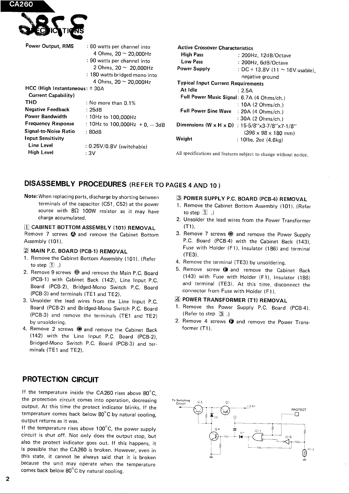
ToSw;tch;ng 03
:"' --Q
I ~'
--,0,----..2
D W i--
_138V
'" J
PROTECT
r~l
'~i...
Page 5
ALIGNMENT PROCEDURES
(REFER TO PAGES 9 AND 10 )
-Idling current adjustment
Conditions:
-Connect the DC
between TP3 and TP4.
-Connect a 13.8V power
voltmeter between TPl and TP2 and
supply to the 12V
Power In terminal.
-After the power on
ing to be sure of the most stable operation.
, wait for 5 minutes before
Adjustment
Note: When replacing or disconnecting a resistor
Inspection:
-Confirm that the
(voltage: 33mV:t 13mV).
Battery
measur-
, disconnect the power supply first.
If the current
specified
, adjust it with the procedure below.
idling current is 50mA :t
20mA
measured does not fall within the range
Current
less than 29mA
71mA ~ 100mA
101mA ~ 200mA
201 mA ~ 250mA
more than 251 mA
less than 19mV
46mV ~ 66mV
67mV ~ 132mV
133mV ~ 165mV
more than 166m V Cut out R479 and R480.
After the adjustment is complete
properly.
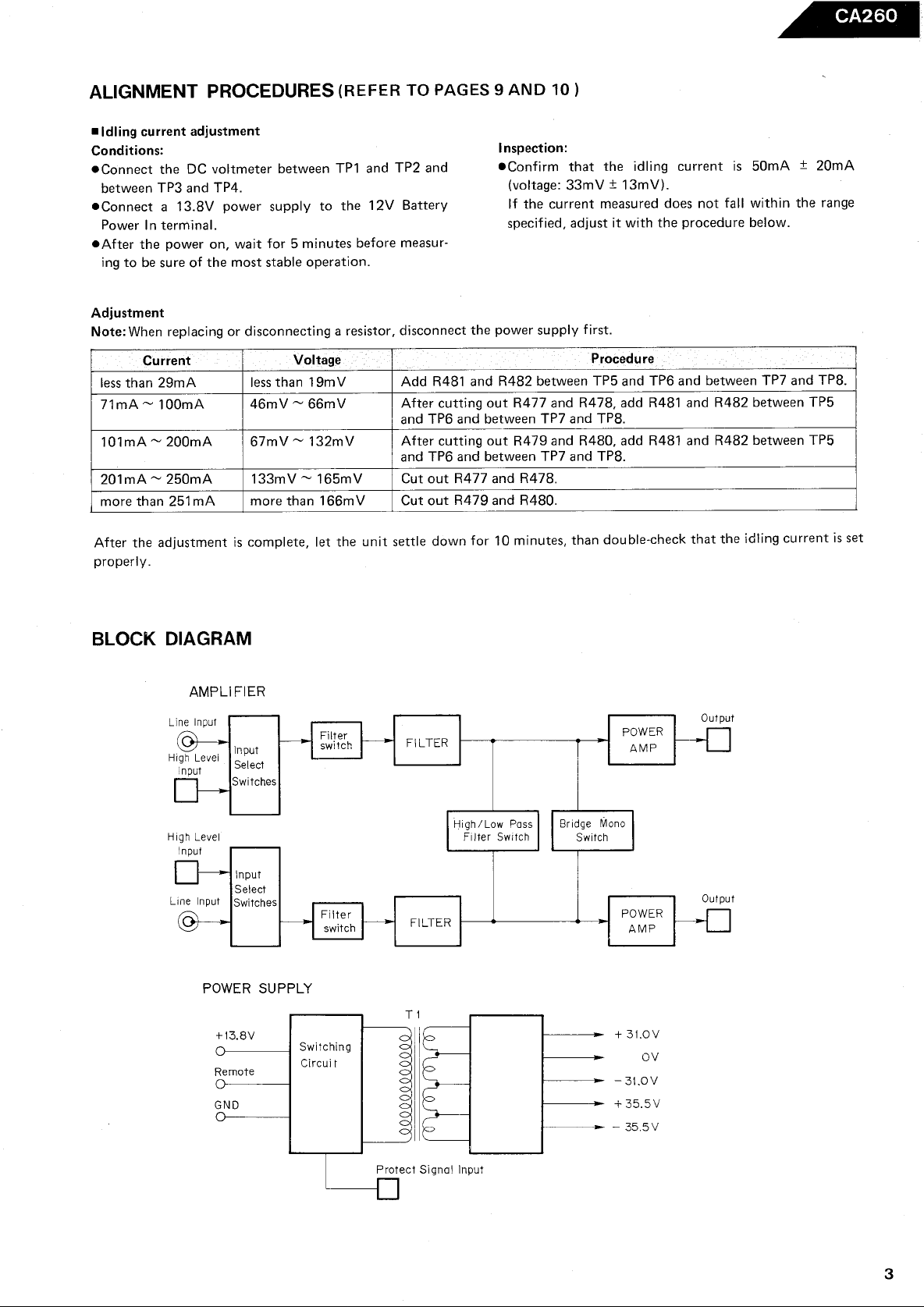
BLOCK DIAGRAM
AMPLI FIER
Line Input
High Level Input
Input
Select
Switches
Voltage
Add R481 and R482 between TP5 and TP6 and between TP7 and TP8.
After cutting out R477 and R478
and TP6 and between TP7 and TP8.
After cutting out R479 and R480, add
and TP6 and between TP7 and TP8.
Cut out R477 and R478.
, let the unit settle down for
FILTER
10 minutes
Procedure
, add R481 and R482 between TP5
R481 and R482 between TP5
, than double-check that the idling current is set
Output
POWER
AMP
Input
Line Input Switches
Select
POWER SUPPLY
+13.
Remote
GND
Switching
Circui t
---0
High/Low Pass
Fi Iter Switch
FILTER
Protect Signa! Input
POWER
Output
AMP
+ 31.0V
- 31.0V
+ 35. 5 V
- 35. 5 V
Page 6
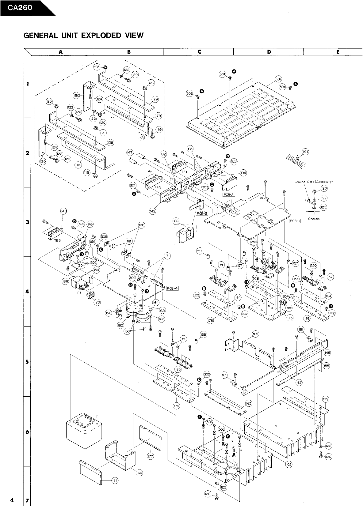
GENERAL UNIT EXPLODED VIEW
Page 7

GENERAL UNIT PARTS LIST
Ref. No.
101
102
119
120
121
122
123
124
125
129
130
142
143
145
147
154
155
156
157
158
159
161
162
163
164
165
166
167
169
170
171
174
175
176
177
179
180
181
183
184
185
186
191
192
193
194
202
250
301
302
303
304
305
306
Part No.
A424-CA260A
CA260A
B222-
7028
2310-
501641
2346-
2440- 70 1 8
2412-
5042
2414-504
401649
2557-
2440- 7019
7035
2218-
2218-7036
12101
14241424-12201
1443-
07701
1662-
05002
11768
21122132-7118
2132-7119
7120
2132-
7123
2132-
2132-7124
2219-7965
7966
2219-
2219- 7967
2219-7968
2219- 7969
7971
2219-
2219-7972
7994
2219-
7995
2219-
7998
2219-
2222- 71 58
2222- 71 59
2222- 7160
2222- 7161
2222- 7163
2222- 7106
2222- 7168
2224-7092
2224- 7093
7094
2224-
2224- 7098
2240- 7120
2240- 7220
2240- 7224
2240- 7225
2440- 7016
YC40B
21142347-3006K7
2347-301026
2347-
300627
2347-
300626
301227
2347-
2557-301229
J30179
ll11-
J30180
llll-
1756-
09901
1221-717169
1222-7267
1222- 7268
I Description
Cabinet Bottom Assembly
Heat Sink Assembly, Right
Hexagon-
Hexagon-Head Tapping Screw
Head Bolt
Hexagon Nut
Spring Washer
Toothed Lock Washer
Bolt
Hexagon Nut
Bracket
Bracket
Cabinet Back
Cabinet Back
Front Panel
Push Button
, Filter Switches
Sponge
Spacer
Spacer
Spacer
Spacer
Spacer
Bracket
Bracket
Bracket
Bracket
Bracket
Bracket
Bracket
Bracket
Bracket
Bracket
Heat Sink
Heat Sink
Heat Sink
Heat Sink
Heat Sink
Heat Sink
Heat Sink
Insulator
Insulator
Insulator
Insulator
Holder
Holder
Holder
Holder
Special Nut
Bushing
Tapping Screw (+) (3 x 6mm)
Self-
Tapping Screw (+) (3 x 10mm)
Self-
Tapping Screw (+) (3 x 6mm)
Self-
Tapping Screw (+) (3 x 6mm)
Self-
Tapping Screw (+) (3 x 12mm)
Self-
Screw with Washer (+) (3 x 12mm)
Owner Guide (for U.
A. model)
Owner Guide (for General & Canada models)
Installation Template (Accessory)
Packing Box
Packing Cushion
Packing Cushion
, Left
, Right
Page 8

ELECTRICAL PARTS LIST
Ref. No.
ffiTl
C429
ffiFl
PT1
TE1
TE2
ffiJ3
LUGl
, 441 442 443 444
, 98
ffiR97
418
R417
R419 420
422
R421
R449 450
R459 460
R465A/B
467 A/B
, 466A!B
, 468A!B
R469, 470, 471 472
R473, 474, 475, 476
R477 478
R479 480
R483, 484
R513
, 485, 486
514
I Part No.
CHASSIS MISCELLANEOUS
5584- 701464
104144
5369-
7935
4472-
5192-
090TSl
4214-148
147
4214-
701107
41634211-
4162-726
736
4162-
4211-
RESISTORS
1014713
5102-
5174-562381
243381
5174-
301381
5174-
561381
5174-
470381
5174-
R33671
5275-
220572
5171-
470572
5171-
151381
5174-
131381
5174-
100381
5174-
243381
5174-
I Description
Power Transformer
:t 10%, 25V
Capacitor, O.
Fuse with Holder
Posistor
Terminal
l/lF
, 30A (Spare Fuse Inclusive)
, ME2
, High Level Input, 12V Battery Power In
Terminal, Speaker System
Connector with Lead Wire
Lug Terminal
Power Cord
Ground Cord
Spade Lug (w/Tube) (Accessory)
1O0D
6kD
24kD
300D
560D
47D :!: 1%, 1/4W
33D
22D :!: 5%
47D
, Red (Accessory)
, Black (Accessory)
, :t 2%, 1/4W
, :!: 1%, 1/4W
, :t 1%, 1/4W
, :t 1 %
:!: 1%, 1/4W
, :!: 10%, 5W x 2, Cement
, 1/4W
, Fuse
, Metal
, Metal
, Metal
, Metal
, Metal
, lW, Metal
, :t 5%, lW
, Metal
150D :!: 1%, 1/4W, Metal
130D
:t 1%
, 1/4W
, Metal
10D :!: 1%, 1/4W, Metal
, :t 1 %
24kD
, 1/4W, Metal
, Semiconductor
C76
C77, 78
C79
C81
C401 402
C405, 406
C407 408
ffiC409
41O 411 412
C413 414
C415 416
C417 418
, 504
, 524
, 64
427
, 505, 506
, 402
ffiC425, 426
C50 1 , 502
C503
C523
D61 , 401
D62
D63
D403, 404, 405, 406
D407, 408
D409, 410, 411 , 412
428
, 413, 414
CAPACITORS
5345-226B041
476D041
5345-
227D041
5345-
5345-225F041
5345-684F0951
5345-337B0226
5345-476C0952
5345-226F041
5359-1015851
5345-476C041
5353-050934
476 F04 1
5345-
106C0952
5345-
106D0952
5345-
5345-226D041
DIODES
1S2473
5631-
MV104V
5641-
HZ15-
5635-
10DF2
5632-
HZ12B2L
5635-
1 S24 71
5636-
22/lF
4Jt.LF
, :t 20%
:t 20%
, Electrolytic
, 10V
, 25V, Electrolytic
220/lF, :!: 20%, 25V, Electrolytic
2/lF
, :!:20%, 50V
, :t 20%
68/lF
, :!: 20%
330/lF
:t 20%
47/lF
22t-tF, :!: 20%, 50V
100pF
47/lF
5pF
47t-tF
10t-tF
10t-tF
22/lF
1 S2473
:!: 5%, 100V
:t 20%
:t 0.
5pF, 500V, Mica
:t 20%
:t 20%
:t 20%
, :t 20%, 25V
, Electrolytic
, 50V, Electrolytic
, Electrolytic
, 1 OV
, 16V, Electrolytic
, Electrolytic
, Polypropylene
, 16V, Electrolytic
, Electrolytic
, 50V
, 16V, Electrolytic
, 25V, Electrolytic
, Electrolytic
Varistor, MV104V
, HZ15-
Zener
10DF2
Zener, HZ12B2L
1 S24 71
Page 9

Ref. No.
031
409 410 415 416
034
417
413 414
418
035 405
408
407
037
040
041
0401 402
0411
0419
403 404
412
420
0421 422
0423, 424
, 426
0425
428
0427
, 430
0429
0431 432
, 434
0433
437 438
436
0435
440 441
0439
0501 502
0503, 504
, 406
L405
406
442
Part No.
TRANSISTORS
5613-2240(BL)
5611-970(BL)
5613-2603(E)
5611-1115(E)
2877(0)
5613-
1217(0)
5611-
1775(F)
5613-
2240(BL)
5613-
646(C)
5612-
5614-666(C)
669(B)
5614-
649(B)
5612-
669(C)
5614-
5612-649(C)
2591 (0)
5613-
1111 (0)
5611-
3182(0)
56135611-1265(0)
999L(F)
5611-
2320L(F)
5613-
COILES
7165
5991-
I Description
2SC2240(BL) or 2SC2240(GR)
2SA970(BL)
2SC2603(E) or 2SC2603(F)
2SAl115(E) or 2SA1115(F)
2SC2877(0) or 2SC2877(Y)
2SA1217(0) or 2SC1217(Y)
2SCl775(F)
2SC2240(BL)
2SB646(C)
2SD666(C)
2SD669(B) or 2SD669(C)
2SB649(B) or 2SB649(C)
2SD669(C)
2SB649(C)
2SC2591 (0) or 2SC2591 (R) or 2SC2591
2SA1111(0) or2SAll11(R) or2SAll11(S)
2SC3182(0) or 2SC3182(R)
2SA1265(0) or 2SA1265(R)
2SA999 L( F)
2SC2320L(F)
(S)
SW1
C519
C521
SW4
, 2
C507
C508
0505
SW3
520
, 522
MISCELLANEOUS
4431-
A04727
PCB-
2 LINE INPUT P.
CAPACITORS
5359-2715851
5359- 1515851
MISCELLANEOUS
4421-
0427126
4482- 711 7
PCB-
3 BRIDGED-
CAPACITORS
5345-475D0952
5345-106D0952
TRANSISTOR
2603(E)
5613-
MISCELLANEOUS
4421-
0227123
Push Switch
C. BOARD
, :t 5%
270p F
, :t 5%
150pF
Slide Switch
Pin Jack
MONO SWITCH P.
, :t 20%
4.7pF
, :!: 20%, 25V, Electrolytic
1 OpF
2SC2603(E) or 2SC2603(F)
Slide Switch
, Filter ON/OFF
, Polypropylene
, 1 OOV
, Polypropylene
, 1 OOV
, Line Input Sensitivity
, Line Input
C. BOARD
, Electrolytic
, 25V
, Bridge Mono
, High Pass/Low Pass Filter
Page 10

Ref. No.
I Part
No.
I Description
R24
, 29, 30, 31 , 32, 33
6Cl
, 4, 5, 6
C9,
C12
C13
C18
6C51
6C53
, 54
6C55
, 56, 57, 58
IC1
IC3
IC4
IC5
12,
016
, 17
018
20,
RESISTOR
184381
5174-
CAPACITORS
5345-
227D0921
5345-107 -
5345-227 A041
5345-225F041
5359-
3315851
5359-2015851
5345-106-
105-
5345-
109F0960
53415345-476F041
5345-226F041
180kD
220pF
100pF
220pF
2pF
330pF
200pF
:t 20%
10pF
:t 20%
lpF
10000pF
:t 20%
47pF
:t 20%
22pF
, :t 10%
:t 20%, 25V
:t 20%, 25V
:t 20%
:t 20%
:t 5%, 100V
:t 5%
INTEGRATED CIRCUITS
5654-MN4011 B MN4011 B
5654-MN4069UB MN4069UB
5654-MN4027B
5652-
M5223P M5223P
MN4027B
TRANSISTORS
5611-
1286(H)
5613-
2603(E)
5613-3246(H)
3345(0)
5613-
5613-
2626
2SA 1286(H)
2SC2603(E) or 2SC2603(F)
2SC3246(H)
2SC3345(0) or 2SC3345(Y)
2SC2626
, 1 /4W, Metal
, Electrolytic
, Electrolytic
, 6.
3V, Electrolytic
, Electrolytic
, 50V
, Polypropylene
, Polypropylene
, 100V
, Electrolytic
, 16V
, Electrolytic
, 50V
:t 20%, 50V
, Electrolytic
, 50V
, Electrolytic
, 50V
, Electrolytic
, 7
10,
, 9,
6D3, 4, 5 , 53
D12
D14
D15
6D51
L51,
, 54, 55
DIODES
E RCOl 02F
56325631-1S2473
5632-
10DF2
5635-HZ6A-
5635-HZ9B-
5637-GL5HD10
5637-GL5HY10
PB101 F
5685-
COILS
5991-7175
ERC0102F
1S2473
10DF2
Zener
, HZ6A-
Zener
, HZ9B-
, GL5HD10, Power Indicator
LE.
, GL5HY10, Protect Indicator
LE.
Bridge Silicon, PB 101 F
, Red
, Amber
Page 11

g~~~
C421
R69
/l/lF
PRESENT SAFETY
COMPONENTS MUST ONLY BE REPLACED BY ORIGINAL PARTS.
3t,
::~:.
~----,
J""
Q401
2sel7751FJ TE2
C401
/50V
R457
220K
R4I3
o,\F)
Q407
2sIC2603(E)
R99
35.
C79
"O/25V
47/25V
$ C77
47/25V
. C78
cao
"0/25 V
r.. --
R539
:'so
:'sO
Q402
2Sel775(FJ
C402
66/50V
R458
220K
Q408
2SC2603
\E)o,\F)
I L
D408
HZI2B-2L
3tOV
PROTECT
PT2
SWITCHING
TRANSISTOR
SENSOR
KD = 1 OOO~ MD = 1000KD.
1. ALL RESISTANCES VALUES ARE IN D.
NOTES
2. THE WATTAGE OF RESISTORS IS 1/4W UNLESS OTHERWISE NOTED.
3, ALL CAPACITANCES VALUES ARE IN /IF UNLESS OTHERWISE NOTED, P=
ill REGULATIONS, THESE
5. ~ SAFETY-REQUIREMENTS COMPONENTS IN ACCORDANCE WITH
4. V: DC VOLTAGE AT NO SIGNAL
'25V
C504
C516
*0.
FiI", ON/OFF
H;gh Po35/Low Po" Flit.,
B';dge-Mona
Line 'op", Sen5;,;vlty
SWI
SW3
SW2
SW4
l!:.
R523
560
R505
560
.,.
R 506
z:'
SIGNAL
Lch t;:;',
JI PA
R ch
TE1
HIGH LEVEL INPUT
lei MN40llB
IC 4
MN4027B
3-9
RII
lei MN40llB
IOOOP
SCHEMATIC DIAGRAM
Page 12

C519, 520
C521 , 522
041
040
C405, 406
R421
, 422
R419, 420
Ref. No,
Signal-to-
Input Sensitivity
Line Level
High Level
Frequency Response
Noise Ratio
THD (4 Ohms/2 Ohms)
Negative Feedback
Power Bandwidth
Current Capability)
HCC (High Instantaneous: ::I: 30A
SPECIFICATIONS
Power Output, RMS
74B FOR ALL OTHER PARTS AND SERVICE INFORMATION.
Model CA260
HIGH FIDELITY CAR AMPLIFIER
MODIFICATIONS WERE MADE AT SERIAL NUMBER 9008201 TO IMPROVE PERFORMANCE.
EXCEPT FOR THE CHANGES AS NOTED IN THIS SUPPLEMENT, REFER TO MANUAL 74A AND
The
Harman Kardon
CAPACITORS
5359-
5359-
4715851
2715851
470pF, ::1:5%, 100V, Polypropylene
270pF, ::1:5%, 100V
, Polypropylene
harman/kardon
240 Crossways Park West
l112-H15274C P-088511 1650
TRANSISTORS
5613-3422(0)
5611-
1359(0)
2SC3422(0) or 2SC3422(Y)
2SA 1359(0) or 2SA 1359(Y)
CAPACITORS
5345-
477C0952
470"F, ::1:20%, 16V
, Electrolytic
5174-393381
5174-
221381
39kO
2200 ::I: 1 %, 1/4W
, ::I: 1 %, 1/4W
, Metal
, Metal
RESISTORS
I Part No.
: 0.
: lV
1 V /0. 5V (switchable)
: 10Hz to 100 000Hz
: 10Hz to 100,000Hz + 0, - 3dB
: 80dB
ELECTRICAL PARTS LIST
I Description
Weight
Specifications and components subject to change without notice,
Overall performance will be maintained or improved,
Dimensions (W x H x D)
: 101bs. 20z. (4.
: 30A (2 Ohms/ch.
: 15-
(396 x 98 x 180 mm)
5/8" x 3-
: No more than 0, 1 %/0.
: 25dB
Full Power Music Signal: 6.
Full Power Sine Wave
: lOA (2 Ohms/ch.
: 20A (4 Ohms/ch.
7A (4 Ohms/ch.
: 180 watts bridged mono into
4 Ohms, 20- 20 000Hz
2 Ohms, 20- 20
000Hz
Typical Input Current Requirements
Power Supply
At Idle
: 2.
: DC + 13.8V (11 - 16V usable),
negative ground
: 60 watts per channel into
: 90 watts per channel into
4 Ohms, 20- 20, 000Hz
Active Crossover Characteristics
High Pass
Low Pass
: 200Hz
: 200Hz, 6dB/Octave
, 12dB/Octave
SUPPLEMENTARY MANUAL
f,. "
, Woodbury,
PrintedlnJapan
11797
6kg)
7/8" x 7- 1/8"
Manual 74C
Page 13

WIRING DIAGRAM
IpCB-11
BLK
C429
SW4
LINE INPUT
SENSITIVITY
LINE INPUT
J2
HIGH LEVEL INPUT
TE1
L J 1
SW2 SVfI
HIGH PASS---
LOW PASS
--- 0
FILTER
SPEAKER SYSTEM
TE2
OFF
SW3
BRIDGE MONO
PIN CONNECTION DIAGRAM OF TRANSISTORS
28C2240
28A970
25C1775
28A999L
28C2320L
28C2603 28C2877 28B646
28A 1115 2SA 28D666
28D669 'QI 2SA12
28B649 28C3246
C B
, DIODES AND ICS.
28C3345 28C2626
28C2591
C E
28C3182
2SA
C E
182473
HZ15-2L
10DF2
HZ12B2L
182471
EROCO1 02F ,.."'"
HZ6A- Anode
HZ9B-2L '
~A"'"
DIODE
MV104V GL5HD10 PB101
Cathode
GL5HY10
Anode
Page 14

\--' "::"';::':;' ,
Page 15

eLK
eLK
eLK
eLK
PROTECT
IND.
POWER
IND.
SYSTEM
FI30A
GND
+8 REMOTE
12V BATTERY POWER
TE3
PT2
Anode
PB101F
MN4011 B
MN4
14
POWER
M5223P
-WIRE COLOR ABBREVIATIONS
: Red
RED
Orange
ORG :
Blue
BLU :
WHT : White
GRN : Green
BLK : Black
VEL : Yellow
: Purple
PUP
Pink
PIK :
Page 16

: :
C:::'::::;::"
Page 17

SAFETY
J.lJ.lF
COMPONENTS MUST ONLY BE REPLACED BY ORIGINAL
J.lF UNLESS OTHERWISE NOTED. P=
, THESE
REQUIREMENTS COMPONENTS IN ACCORDANCE WITH PRESENT
VOLTAGE AT NO SIGNAL
PARTS.
ill REGULATIONS
5, '" SAFETY-
CAPACITANCES VALUES ARE IN
WATTAGE OF RESISTORS IS 1!4W UNLESS OTHERWISE NOTED,
4, V: DC
3. ALL
2. THE
K.!1=1000.!1 , M.!1=1000K.!1.
1, ALL RESISTANCES VALUES ARE IN.!1.
10K
R48
10 K
R49
OWl
033
C420
~ 0.
OW)
R474
R4722210WJ.(;:R476
R470 22 lOW)
L406
C424
12K
R440
PROTECT
31.0V
17/50V -35.
35.
31.ov .
31.0V
C 54
17/50V
C53
/50V 1-
10000
(jJ C52
10000/Sov
(jJ C51
. L
-31,
HZI2B2L
D408
R41S
:9iNv-
-13
R426
34.
5 P
C41S
560
R416
12.4V
2slc2240(BL)
Q404
2SC2240
Q402
(EJor(F)
2SC2603
Q408
220K
R458
13)
6S/50V
C402 (BL)
(3;) R
e SYSTEM
SPEAKER
TE2
GR)
OW)
R475
C419
~ 0.033
lOW)
R76
OW)
R473
R47t 22
R469 22 low)
L405
2SC2240( BL) ore
Q31
47K
R82
31.OV
C422 0,
22K
4,6V
R432
Q39
'/ or(FJ
~SAI1I5(E)
(jJ
22/50V
C411
D414
35,
1006 -3S.
I or(Y)
1217(O)~ ~I
32L
92L
or(F)
22 K
R413
2sIC2603(E)
Q407
/50V
C401
220K
R457
R99
3S.
reV)
.c~
,:"
R69
C421
....
1.5K~1.5K
R405,2 R407
J--
--
~-----,
"///
Page 18

" ", ,-. ':':" ::,
Page 19

IC3: TC4069)JBP
IC I : TC4011 BP
33 K
REMOTE
R I
152473
GND +8
IC2: TC401lBP
100/25
R25
180K 15K
R24
200P
C 12
::J
1--
3V
I C I
ICI:TC40IlBP
E!J C
lOOK
R30
CI4
IC5: M5223P
TC4069)JBP
IC 3
C I
1000P
10 K
R23
PT I
(1/2W)
R53
470
R538
C518
22011/2W)
R 15
13.
L_-
I ~ 0,
R508
R 524
RI2
RII
560
R 506
L_-
IC 4
lC1: TC40llBP
3-9
TC4027BP
110
r-:
SW3
lOOK
R5~3
220/25 V
C80
C79
14.
220/25V
t4,
330
R520
13,
10/25V
R519
470
C504
10/25V
C503
C515
R517 R537
470
R535
~ 0,
R515
Input Sensitivity
Bridge-Mono
Poss /Low Poss Filter
'Filter ON/OFF
2SA999L(F)
Q501
01
C513
SW4 'Line
SW3 "
SW2 'High
SW I
~O'
C517
r--.
R523
R507
560
R505
R ch
L ch
Rch
L ch
J 1
HIGH LEVEL INPUT
TE1
LINE INPUT
14. 5V'
r.--
5WI
R539
5W2
lOOK
R521
330
SCHEMATIC DIAGRAM
(!)
 Loading...