

Page 1
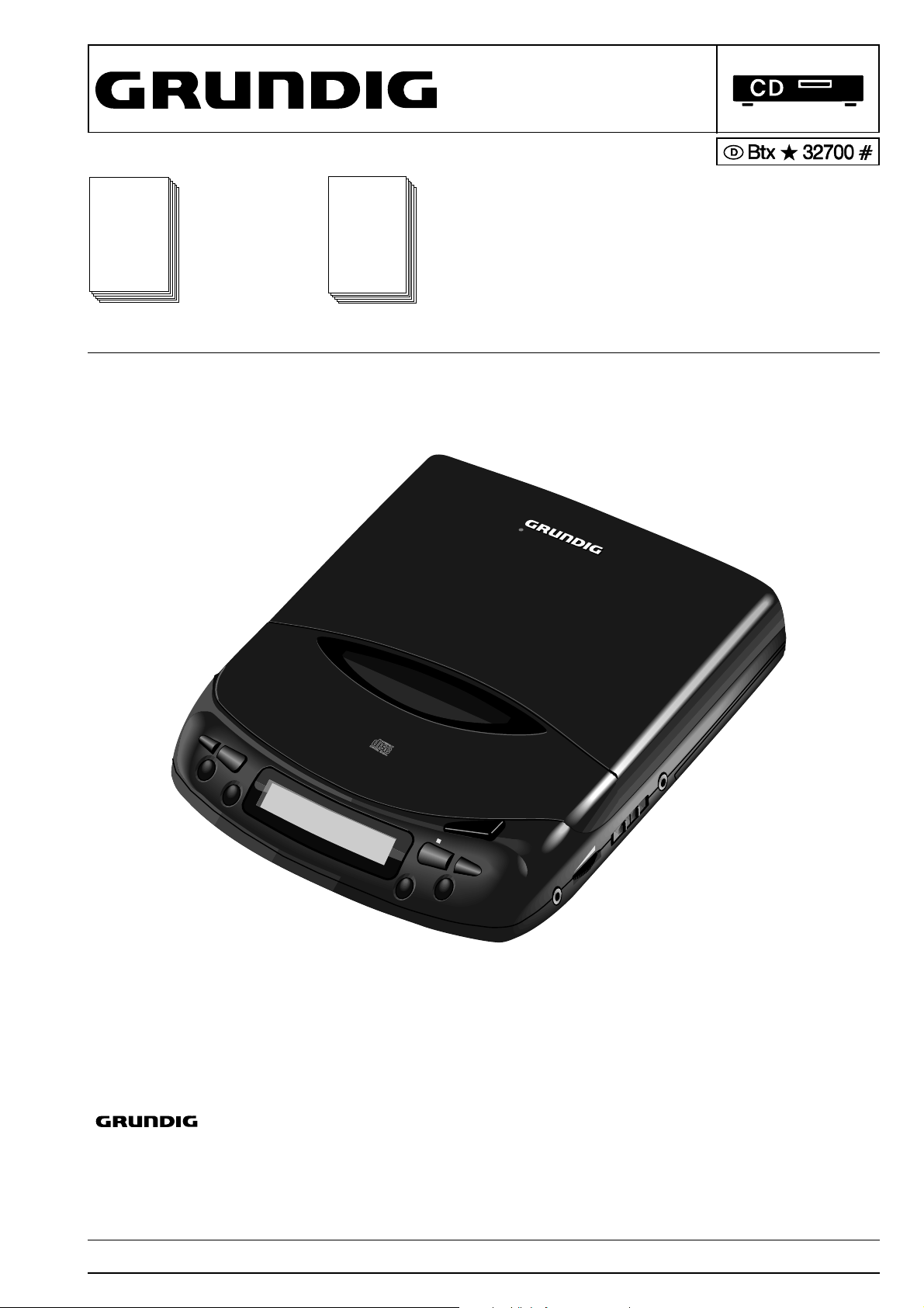
SERVICE MANUAL
Service
Manual
K-CDP 65
Sach-Nr./Part No.
72010-743.90
Zusätzlich erforderliche Unterlagen
für den
Komplettservice:
Additionally
required Service
Manuals for the
Complete Service:
Service
Manual
Sicherheit
Safety
Sach-Nr./Part No.
72010-800.00
TIMES OVERSAMPLING
ULTRA BASS SYSTEM
K-CDP 65
§
INTRO
§
REPEAT
TRACK MIN SEC
K-CDP 65 (75.5073-1051 / G.DF 90-51Y)
RAN.
STOP
2;
PROGR.
PLAY/
PAUSE
OPEN
HEADPHONE
VOLUME
BASS BOOST
OFF ON
LINE OUT
Änderungen vorbehalten Printed in Germany Service Manual Sach-Nr. 72010-743.90
Subject to alteration VK 23 0595 Service Manual Part No. 72010-743.90
Page 2
Allgemeiner Teil / General Section K-CDP 65
Es gelten die Vorschriften und Sicherheitshinweise gemäß dem Service Manual "Sicherheit",
Sach-Nummer 72010-800.00, sowie zusätzlich
die eventuell abweichenden, landesspezifischen
Vorschriften!
D
Inhaltsverzeichnis
Seite
Allgemeiner Teil....................................1-2…1-5
Meßgeräte / Meßmittel................................................................. 1-2
Servicehinweise ........................................................................... 1-2
Technische Daten ........................................................................ 1-2
Bedienhinweise ........................................................................... 1-3
Ausbauhinweise.......................................................................... 1-5
Abgleich .......................................................... 2-1
Platinenabbildung
und Schaltplan ......................................3-1…3-9
Platinenabbildung ........................................................................ 3-1
Schaltplanabbildung.................................................................... 3-3
IC-Beschreibung ......................................................................... 3-5
The regulations and safety instructions shall be
valid as provided by the "Safety" Service Manual,
part number 72010-800.00, as well as the
respective national deviations.
GB
Table of Contents
Page
General Section .....................................1-2…1-5
Test Equipment / Jigs .................................................................. 1-2
Service Hints................................................................................ 1-2
Specifications............................................................................... 1-2
Operating Instructions................................................................. 1-3
Disassembly Instructions ............................................................ 1-5
Adjustment Procedures................................. 2-2
Layout of the PCB
and Circuit Diagram ............................3-1…3-9
Layout of the PCB ........................................................................ 3-1
Circuit Diagram ............................................................................ 3-3
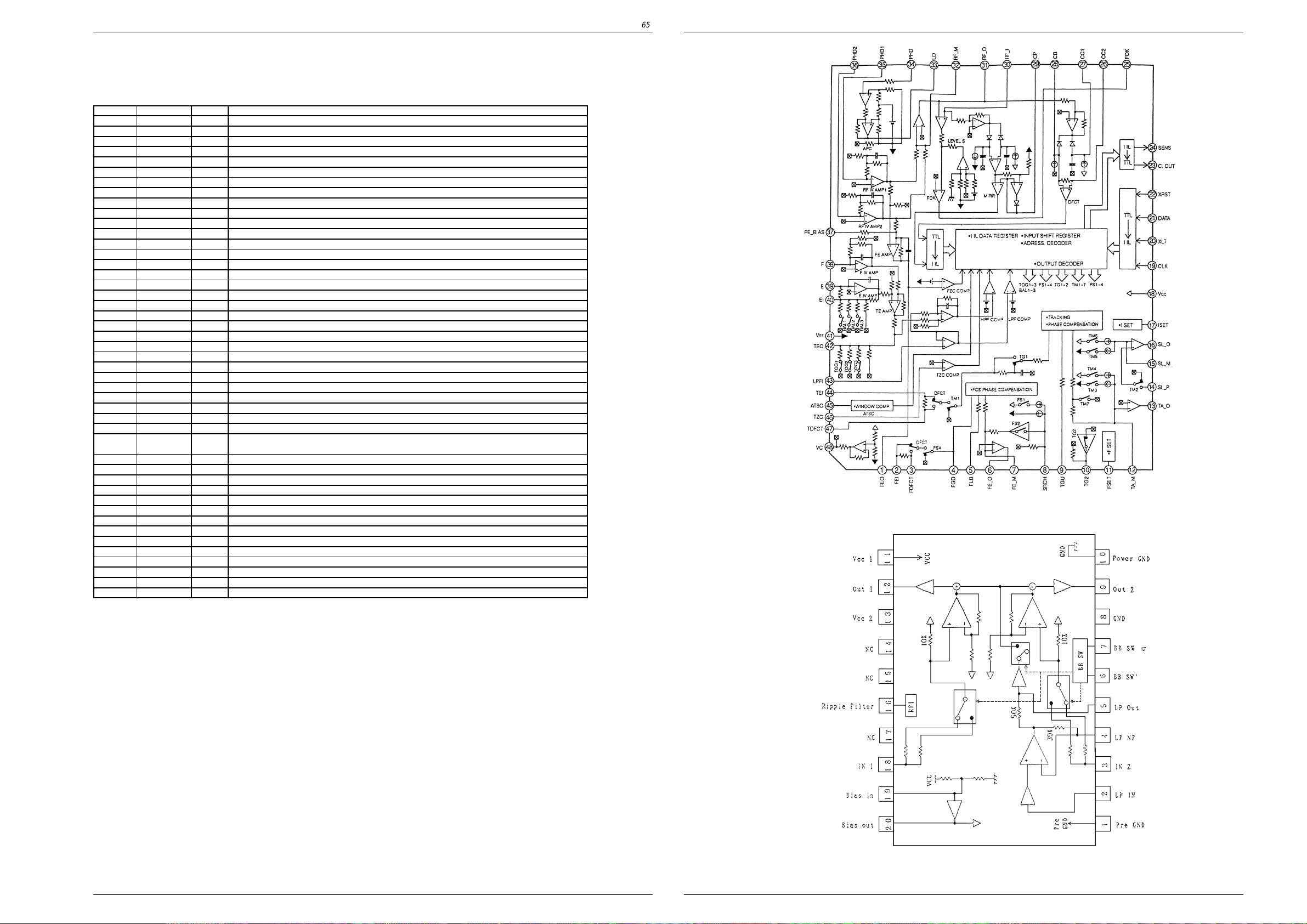
IC -Description ............................................................................. 3-5
Explosionszeichnung
und Ersatzteilliste .................................4-1…4-3
Explosionszeichnung .................................................................. 4-1
Ersatzteilliste............................................................................... 4-2
Allgemeiner Teil
Meßgeräte / Meßmittel
Oszilloskop, DC-Voltmeter, NF-Voltmeter, Test-CD Sach-Nr.: 72008-
376.00
Beachten Sie bitte das Grundig Meßtechnik-Programm, das Sie unter
folgender Adresse erhalten:
Grundig electronics GmbH
Würzburger Str. 150, D-90766 Fürth/Bay.
Tel.0911/703-0, Telefax 0911/703-4479
Technische Daten
Frequenzgang............................................................. 20-20.000 Hz
D/A -Umsetzung.................................... 1 Bit linear 4 fs digital Filter
Ausgangspegel (4,5V Eingang) ............................................ 500 mV
Line Ausgang ........................................................... Stereo mini jack
Stromversorgung:
AC: Netzadapter 230 V
DC: 2 LR 6 (AA) Alkali-Batterien oder Akkus
Leistungsaufnahme........................................................... 1,0 W DC
Abmessungen (BxHxT) .................. ca. 131 mm x 29 mm x 153 mm
Gewicht ................................................................................ca. 300g
Zubehör (mitgeliefert)....................... Netzadapter, Stereo Kopfhörer
Exploded View and
Spare Parts List ....................................4-1…4-3
Exploded View ............................................................................. 4-1
Spare Parts List ........................................................................... 4-2
General Part
Test Equipment / Aids
Oscilloscope, DC Voltmeter, AF Voltmeter, Test CD Part No.: 72008-
376.00
Please note the Grundig Catalog "Test and Measuring Equipment"
obtainable from:
Grundig electronics GmbH
Würzburger Str. 150, D-90766 Fürth/Bay.
Tel.0911/703-0, Telefax 0911/703-4479
Technical Specifications
Frequency response .................................................... 20-20.000 Hz
D/A conversion..........................................1bit linear 4 fs digital filter
Output (at 4.5 V input level) .................................................. 500 mV
Line output ............................................................... stereo mini-jack
Power Supply:
AC: using the AC adaptor 230 V
DC: two LR 6 (AA) alkaline-batteries or accumulators
Power consumption ........................................................... 1.0 W DC
Dimensions (WxHxD).............. Approx. 131 mm x 29 mm x 153 mm
Weight............................................................. Approx. 300g (10 oz)
Supplied accessories .......... AC power adaptor, Stereo headphones
1-2 GRUNDIG Service
Page 3
K-CDP 65 Allgemeiner Teil / General Section
Servicehinweise
CD-Laufwerk
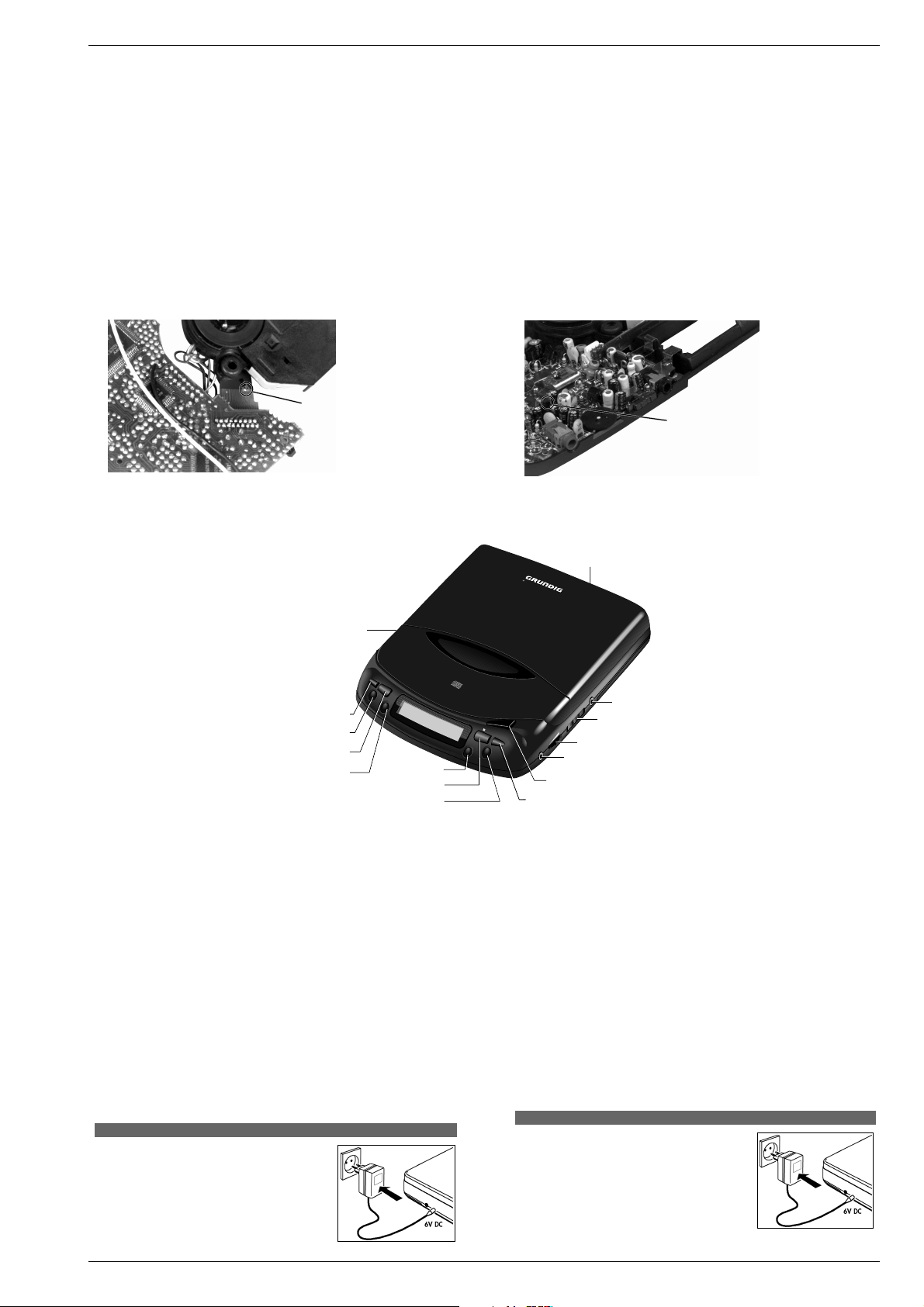
Bei Ausbau des CD-Laufwerkes muß vor Abziehen der Steckverbindungen eine Schutzlötstelle am Flexprint angebracht werden,
um eine Zerstörung der Laserdiode durch statische Aufladung zu
vermeiden.
Beim Einbau eines neuen CD-Laufwerks muß nach Einstecken der
Steckverbinder die werksseitig angebrachte Schutzlötstelle entfernt
werden.
Wiedergabe bei abgenommenen Gehäuseoberteil
Bei abgenommenen Gehäuseoberteil muß der Schalter S309 kurzgeschlossen werden, damit das Gerät arbeitet. Achtung: Bei Betrieb
mit geöffnetem Gehäuse, Laservorschriften (siehe Service Manual "Sicherheit") beachten.
Lötstelle
Solder Pads
Bedienhinweise
Hinweis:
Dieses Kapitel enthält Auszüge aus der
Bedienungsanleitung. Weitergehende
Informationen entnehmen Sie bitte der
gerätespezifischen Bedienungsanleitung, deren Sachnummer Sie in der entsprechenden Ersatzteilliste finden.
POWER
ON/OFF
Service Hints
CD Mechanism
When removing the CD mechanism a safety solder must be attached
at the flexprint to avoid distroying the laser diode by electrostatic
charges.
When reassembling a new CD mechanism the saftey solder which was
attached by the manufacturer must be removed after the wires are
connected.
Playback with Removed Cabinet Top
With removed cabinet top S309 must be shorted so that it is possible
to operate the set. Attention: Take care of the Laser Safety
Instructions (see Service Manual "Safty") when operating the set
with opened cabinet.
S309
Operating Hints
Note:
This chapter contains excerpts from
the operating instructions. For further
particulars please refer to the
appropriate user instructions the part
number of which is indicated in the
relevant spare parts list.
TIMES OVERSAMPLING
ULTRA BASS SYSTEM
DC IN 4.5V
§
§
INTRO
REPEAT
S
INTRO
TRACK MIN SEC
T
REPEAT
RAN.
9 STOP
PROGR.
LINE OUT Buchse für den Anschluß an eine HiFi-Stereoanlage
BASS BOOST OFF/ON
Wahlschalter zum Anheben der Bässe
E VOLUME Lautstärkeregler für den Kopfhörerausgang
HEADPHONE Kopfhörerbuchse (3,5 mm Stereo-Klinke)
OPEN Taste zum Öffnen des CD-Spielerdeckels
PLAY/PAUSE 2; Taste zum Starten und Unterbrechen der Wiedergabe (PAUSE)
PROGR. Taste zum Speichern von Musiktiteln in einem Programm
und zum Überprüfen dieses Programmes
STOP 9 Taste zum Beenden der Wiedergabe und zum Löschen diverser Einstellungen
RAN. Taste zur Wiedergabe aller Titel einer CD in zufälliger Reihenfolge
REPEAT Taste zur Wiederholung eines oder aller Titel der CD
S Taste zum Wählen des vorhergehenden Musiktitels
oder bei längerem Drücken einer beliebigen Stelle der CD
INTRO Taste zur Wiedergabe der ersten 10 Sekunden jedes Titels
T Taste zum Wählen des nächsten Musiktitels
POWER ON/OFF Schalter zum Ein- und Ausstellen des CD-Spielers. Setzen Sie den Schalter
oder bei längerem Drücken einer beliebigen Stelle der CD
immer in die Position OFF wenn Sie das Gerät nicht benutzen.
DC IN 4.5 V Buchse für externe Stromversorgung
Batteriefach
(in Geräteunterseite) Zum Einlegen von 2 LR 6 (AA) Alkali-Batterien oder
aufladbaren Batterien.
STROMVERSORGUNG
Netzadapter (mitgeliefert)
1 Achten Sie darauf, daß die Spannung des
Adapters mit der örtlichen Netzspannung übereinstimmt.
2 Verbinden Sie den Netzadapter (4,5 V/800 mA Gleichspannung,
Pluspol am Mittelstift) mit der Buchse DC IN 4.5V des CD-Spielers
und der Wandsteckdose.
• Trennen Sie den Adapter immer vom Netz, wenn Sie ihn nicht
benutzen.
UT
LINE O
LINE OUT
ST
O
N
BASS BO
FF O
O
E
E VOLUME
HEADPHONE
BASS BOOST
OFF/ON
OPEN
STOP
PLAY/
2;
PAUSE
PROGR.
RAN.
LUM
VO
NE
O
PH
HEAD
OPEN
2; PLAY/PAUSE
LINE OUT Jack for connection to a HiFi installation
BASS BOOST OFF/ON
Selector to boost the bass response
E VOLUME Control for adjusting the volume at the headphone output
HEADPHONE Headphone control jack (3.5mm)
OPEN Button for opening the lid of the CD player
PLAY/PAUSE 2; Button for starting and pausing CD play
PROGR. Button for storing tracks in a program and for checking the program
STOP 9
Button for stopping CD play and deleting various settings
RAN. Button to play the titles of a CD in random order
REPEAT Button to repeat one track or all tracks of a CD
S Button for selecting the previous music track or,
if held down, for searching a particular passage on the CD
INTRO Button to play only the first 10 seconds of each title
T Button for selecting the next music track or,
POWER ON/OFF Selector for switching the CD player on and off.
if held down, for searching a particular passage on the CD
Set the selector always to the OFF position when the set is not in use.
DC IN 4.5 V Jack for external power supply
Battery compartment
(on the bottom of the unit) For inserting 2 LR 6 (AA) alkaline batteries or
rechargeable batteries.
POWER SUPPLY
Mains adapter (supplied)
1 Make sure that the local voltage corresponds to the voltage of the
adapter.
2 Connect the supplied mains adapter (4.5 V/800 mA Direct Current
plus-pole to the center pin) to the player's DC IN 4.5V jack and to
the wall outlet.
• Always disconnect the adapter if you are not using it.
GRUNDIG Service 1-3
Page 4
Allgemeiner Teil / General Section K-CDP 65
Y/
E
O
PEN
HEADPHO
NE
VO
LUM
E
TIMES OVERSAMPLING
ULTRA BASS SYSTEM
LINE OUT
CD IN
(AUX, LINE IN)
Y/
E
OPEN
H
E
A
D
P
H
O
N
E
V
O
L
U
M
E
TIM
ES O
VE
RS
AM
PLIN
G
U
L
TR
A
BA
SS
SYS
TEM
LINE OUT
CD IN
(AUX, LINE IN)
STROMVERSORGUNG
Batterien, Typ LR6, UM3 oder AA
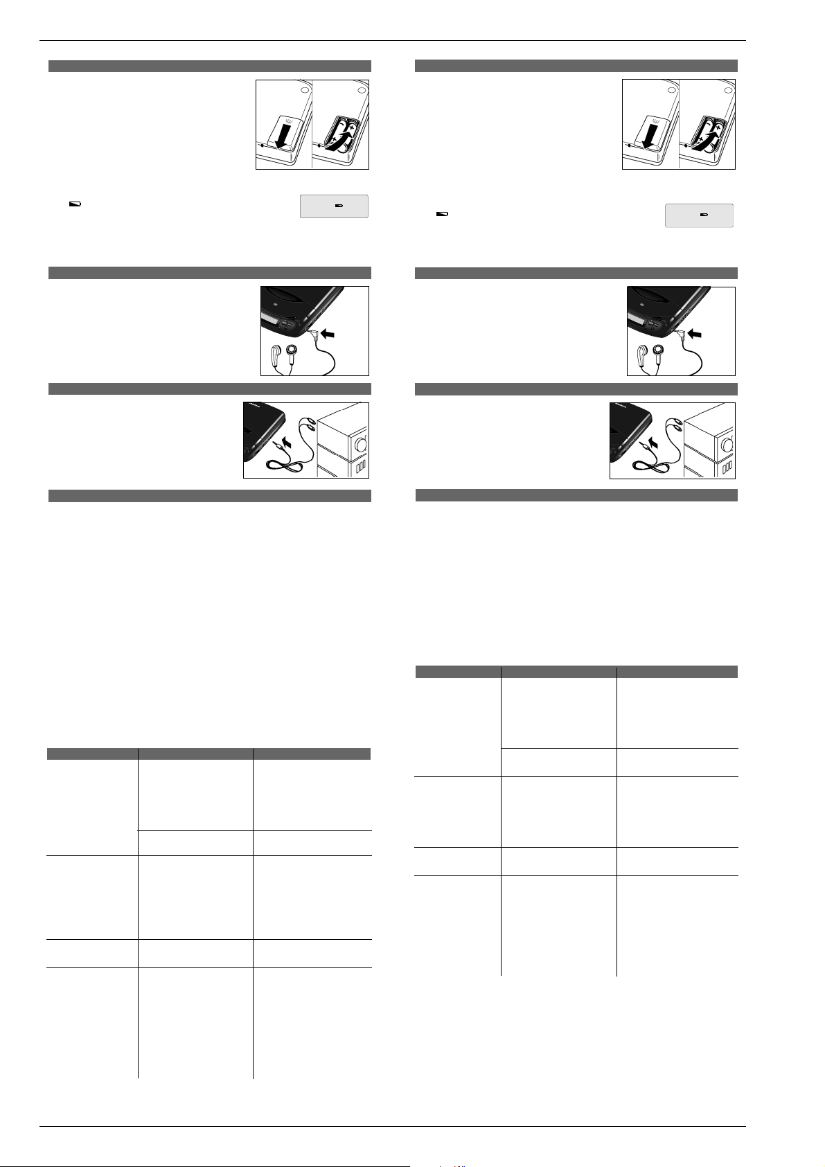
• Öffnen Sie das Batteriefach und legen Sie zwei Alkali-Batterien
Typ LR6,UM3, AA oder zwei aufladbare NiCd-Batterien ein.
Durchschnittliche Betriebszeit unter normalen Bedingungen:
-Alkali-Batterien: 2 Stunden
-NiCd-Batterien: 1 Stunde
• Entfernen Sie die Batterien, wenn Sie leer sind oder längere Zeit
nicht benützt werden.
Die Stromversorgung über die Batterien wird abgeschaltet, sobald die Buchse DC IN 4.5V in Gebrauch ist.
Um auf die Versorgung der Batterien zurückzuschalten, ziehen Sie den Stecker aus der Buchse DC IN 4.5V.
Im Display wird Ihnen angezeigt, wenn die Batteriespannung zu gering ist:
Wenn
erscheint, sollten Sie die Batterien austauschen oder aufladbare
Batterien aufladen.
Umwelt-Hinweis
Verbrauchte Batterien nicht in den Hausmüll werfen!
Geben Sie bei Neukauf die alten Batterien bei Ihrem Händler oder an den öffentlichen Sammelstellen ab.
04
00:58
2
HEADPHONE – Kopfhörerbuchse
• Schließen Sie den mitgelieferten Kopfhörer (16-32 Ohm / 3,5 mmStecker) an die Buchse HEADPHONE an.
OPEN
KOPFHÖRER
Bitte beachten Sie...
Durch zu große Lautstärke können Sie sich und andere im
Straßenverkehr gefährden. Wählen Sie deshalb die Lautstärke immer
so, daß Sie Umfeldgeräusche (z.B. Hupen, Rettungsfahrzeuge,
Polizeifahrzeuge usw.) noch wahrnehmen können.
TRACK MIN SEC
STOP
E
PLAY/
M
2;
U
PAUSE
L
O
V
E
N
O
H
P
D
A
PROGR.
E
H
RAN.
LINE OUT – Wiedergabe über HiFi-Stereoanlage
• Drehen Sie die Lautstärke der Stereoanlage zurück.
• Schließen Sie ein Signalkabel an die Buchse LINE OUT des
CD-Spielers und an die Eingangsbuchsen CD IN, AUX(iliary)
oder LINE IN des anderen Gerätes (Verstärker, Recorder, etc.)
an.
• Stellen Sie den Ton mit den Reglern der Stereoanlage ein.
TECHNISCHE DATEN
Frequenzgang 20-20.000 Hz
D/A-Umsetzung 1 bit linear 4 fs digital filter
Ausgangspegel (4.5V Eingang) Line-Ausgang (stereo mini-jack)
Allgemein
Stromversorgung AC: Netzadapter 230 V
Leistungsaufnahme: 1.0 WDC
Abmessungen (BxHxT) ca. 131 mm x 29 mm x 153 mm
Gewicht: ca. 300 g
Zubehör (mitgeliefert): Netzadapter
Dieses Gerät ist funkentstört entsprechend den geldenden EG-Richtlinien. Der Deutschen Bundespost
wurde angezeigt, daß das Gerät in Verkehr gebracht wurde. Ihr wurde auch die Berechtigung eingeräumt,
die Serie auf Einhaltung der Bestimmungen zu überprüfen. Dieses Gerät entspricht der
Sicherheitsbestimmung VDE 0860 und somit der internationalen Sicherheitsvorschrift IEC 65.
• Bei einem auftretenden Problem prüfen Sie bitte zuerst die nachstehenden Punkte, bevor Sie das Gerät
zur Reparatur bringen.
• Wenn Sie das Problem trotz nachstehender Hinweise nicht beheben können, wenden Sie sich bitte an
Ihren Händler oder eine Service-Stelle.
• Versuchen Sie unter keinen Umständen das Gerät selbst zu reparieren, da die Garantie dadurch ihre
Gültigkeit verliert.
Ausgangssignal 500mV rms
DC: 2 LR 6 (AA) Alkali-Batterien oder aufladbare Batterien
Stereo Kopfhörer
PROBLEM MÖGLICHE URSACHE LÖSUNG
Gerät schaltet nicht ein / Batterien
Wiedergabe startet nicht Batterien sind falsch eingelegt Batterien richtig einlegen
Keine Displayanzeige Batterien sind neu eingelegt Drücken Sie PLAY/PAUSE 2;
Wiedergabe startet nicht Deckel des CD-Spielers ist Deckel ganz schließen
oder unterbricht nicht richtig geschlossen
Display: keine Anzeige, Feuchtigkeit hat sich an Linse CD-Spieler einige Zeit in warmer
00 oder DISC angelegt Umgebung stehen lassen
Wiedergabe startet nicht Die RAN.- oder PROGRAM-Funktion Schalten Sie diese Funktionen aus
mit dem ersten Titel ist aktiviert
Kein Ton / schlechte PAUSE ist aktiviert Drücken Sie PLAY/PAUSE 2;
Tonqualität Lockere /falsche Verkabelung Verkabelung überprüfen
Dieser CD-Spieler entspricht den Funkentstörungsvorschriften der Europäischen Union.
Batterien sind leer Batterien auswechslen /
Kontakte sind verschmutzt Kontakte mit einem Tuch reinigen
Netzadapter
Lockere Verkabelung Netzadapter richtig anstecken
CD ist nicht oder falsch eingelegt CD mit der Beschriftung nach oben
CD ist stark zerkratzt Verwenden Sie eine andere CD
CD ist verschmutzt CD reinigen
Lautstärke ist auf Minimum Lautstärke mit VOLUME
gestellt einstellen
Kopfhörer ist falsch aufgesetzt Auf L(links) und R(rechts)-
Kopfhörerstecker ist verschmutzt Stecker reinigen
Starke elektromagnetische Felder Standort oder Verkablung
in der Nähe des CD-Spielers ändern
Elektrostatische Entladung des Drücken Sie einmal S / T
Benutzers über den CD-Spieler oder zweimal PLAY/PAUSE 2;
aufladbare Batterien neu laden
einlegen
Indikation achten
POWER SUPPLY
Batteries, type LR6, UM3 or AA
• Open the battery compartment and insert as indicated two
alkaline batteries type LR6,UM3, AA or insert two rechargeable
Nickel-Cadmium batteries .
Approx. playing times under normal conditions:
-Alkaline batteries: 2 hours
-Rechargeable batteries: 1 hour
• Remove the batteries if they are empty or if the
CD player is not to be used for a long time.
The battery supply is switched off when the DC IN 4.5V socket is in use. When changing over to battery
supply, pull out the plug from the DC IN 4.5V socket.
The display indicates when the battery voltage is too low:
When appears you should replace or recharge weak rechargeable batteries.
Note on Environmental Protection
Do not throw exhausted batteries in the household refuse. Hand over the old batteries to your dealer or
public collecting points when buying new ones.
HEADPHONE CONNECTION – headphone control jack
• Connect the supplied headphones (16-32 ohms /3.5mm jack plug)
to the HEADPHONE jack.
USING HEADPHONES
Caution...
Do not play your headphones at a high volume. Operation at high
volume can endanger yourself and others in traffic. You should
therefore always adjust the volume so that you can still notice ambient
noises (e.g. horns, rescue vehicles, police cars, etc.)
TRACK MIN SEC
STOP
2;
PROGR.
RAN.
LINE OUT CONNECTION – reproduction through a stereo system
• Turn down the volume of your stereo system.
• Connect a signal lead to the LINE OUT jack of the CD player
and to the input jacks CD IN, AUX(iliary) or LINE IN of the
other set (amplifier, receiver, radio cassette recorder etc.).
• Adjust the sound with the controls of the stereo system.
TECHNICAL SPECIFICATIONS
Frequency response 20-20,000 Hz
D/A conversion 1 bit linear 4 fs digital filter
Output (at 4.5V input level) Line output (stereo mini-jack)
General
Power Supply AC: using the AC adaptor 230 V
Power consumption: 1.0 WDC
Dimensions (wxhxl) Approx. 131 mm x 29 mm x 153 mm
Weight: Approx. 300 g (10 oz)
Supplied accessories: AC power adaptor
• If a fault occurs, please check the points listed below before taking your set for repair.
• If you are not able to remedy a problem by following these hints, consult your dealer or service facility.
• Under no circumstances should you try to repair the unit yourself, as this will invalidate the warranty
Output level 500 mV rms
DC: two 2 LR 6 (AA) alkaline batteries or rechargeable batteries
Stereo headphones
PROBLEM POSSIBLE CAUSE REMEDY
No power or no Batteries
CD play start Batteries incorrectly inserted Insert the batteries correctly
Display: no indication Use of new batteries Press PLAY/PAUSE 2;
CD play does not start CD lid is not securely closed Close the lid securely
or interrupts Moisture condensation Leave the player in a warm place
Display: no indication, until the moisture evaporates
00 or DISC CD is not or incorrectly inserted Insert a CD, label facing up
Play does not start RAN. or PROGRAM is activated Switch off RAN. or PROGRAM
from the first track
No sound or bad PAUSE is activated Press PLAY/PAUSE 2;
sound quality Loose or wrong connections Check connections
Batteries are empty Change/recharge the rechargeable
Contact pins are dirty Clean them with a cloth
AC power adapter
Loose connection Connect the adapter securely
CD is badly scratched Use another CD
CD is dirty Clean the CD
Volume is not turned up Adjust the volume
Headphones worn the wrong Pay attention to the L (left) and
way round R (right) indications
Headphone plug is dirty Clean the headphone plug
Strong magnetic fields near the Change the players position or
CD player connections
Electrostatic discharge from Press S or T once or
the user via the CD player press PLAY/PAUSE 2; twice
batteries
This set complies with the radio interference requirements of the European Community.
The unit complies with the safety regulations according to VDE 0860 / BS 415 and thus with
the international safety regulations according to IEC 65.
The typeplate is located on the base of the set.
Das Typenschild befindet sich auf der Unterseite des Gerätes.
1-4 GRUNDIG Service
04
00:58
2
OPEN
E
PLAY/
M
U
PAUSE
L
O
V
E
N
O
H
P
D
A
E
H
Page 5
K-CDP 65 Allgemeiner Teil / General Section
Ausbauhinweise
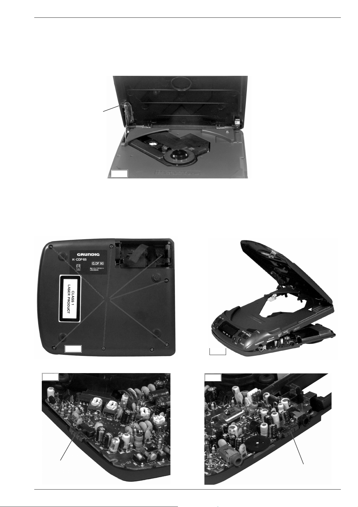
1. CD-Fachdeckel
- CD-Fachdeckel öffnen.
- Schraube a herausschrauben (Fig.1).
- Die beiden Scharnierachsen zu den Geräteaußenseiten schieben
und herausnehmen.
a
c
Fig.1
2. Gehäuseoberteil
- Batteriefachdeckel abnehmen.
- 7 Schrauben b herausschrauben (Fig.2).
- Gehäuseoberteil hinten anheben und abnehmen (Fig.3).
- Achtung: Die Knöpfe der POWER- und BASS/BOOST- Schalter
sind lose (Fig.4,5).
Disassembly Instructions
1. CD Door
- Open the CD door.
- Undo screw a (Fig.1).
- Move the both axles of the hinges to the sides and remove.
c
2. Cabinet Top
- Remove the batterie lid.
- Undo 7 screws b (Fig.2).
- Lift the cabinet top at the rear and remove (Fig.3).
- Attention: The buttons POWER and BASS/BOOST are loosely
(Fig.4,5).
Fig.4
POWER
Fig.2
a
Fig.3
Fig.5
BASS/BOOST
GRUNDIG Service 1-5
Page 6
Allgemeiner Teil / General Section K-CDP 65
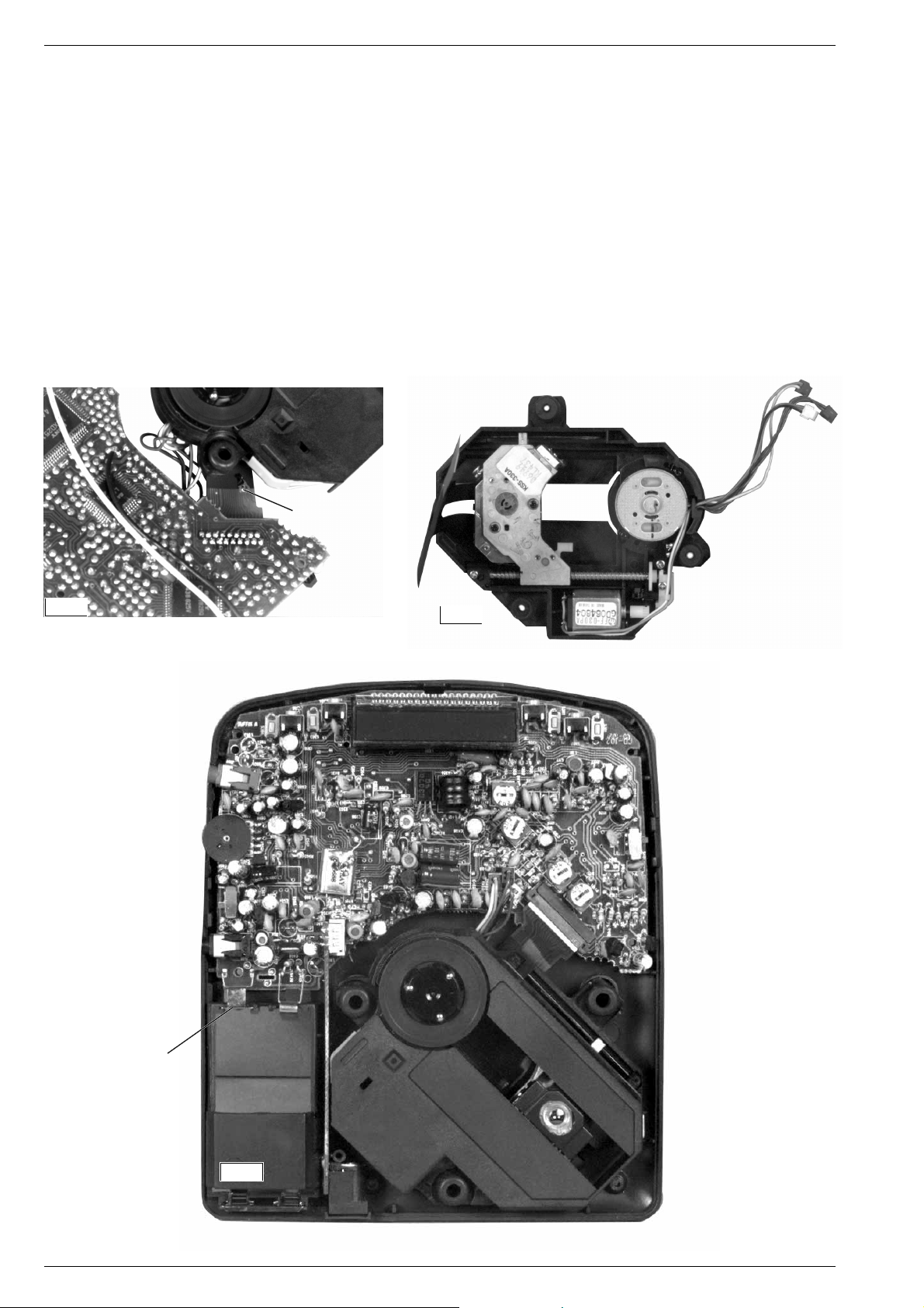
3. CD-Laufwerk
- Gehäuseoberteil abnehmen.
- Vor Abziehen des Flexprints muß die Sicherheitslötstelle (Fig.6)
geschlossen werden, damit die Laserdiode nicht durch statische
Aufladungen zerstört wird. Flexprinthalter öffnen und Flexprint abziehen.
- Steckverbindungen lösen.
- Nach dem Wiedereinbau (auch eines neuen Laufwerks) die
Sicherheitslötstelle wieder öffen.
4. Leiterplatte
- Gehäuseoberteil abnehmen.
- Batteriekontakt c (Fig.8) aus den Führungen ziehen und dabei die
Leiterplatte anheben und herausnehmen.
- Vor Abziehen des Flexprints muß die Sicherheitslötstelle (Fig.6)
geschlossen werden, damit die Laserdiode nicht durch statische
Aufladungen zerstört wird. Flexprinthalter öffnen und Flexprint abziehen.
- Beim Einbau darauf achten, daß der Batteriekontakt in die Führungen eingreift, die Netzteilbuchse in ihren Führungen liegt und der
Steckkontakt der Netzteilbuchsenplatte Kontakt gibt.
Lötstelle
solder pads
3. CD Mechanism
- Remove the cabinet top.
- Connect the safety solder pads before disconnecting the flex print,
to avoid a damage of the laser diode because of static electricity
(Fig.6). Open the flex print holder and pull off the flex print.
- Disconnect the plug-in connections.
- After reassembling the CD mechanism (also a new one) open the
safety solder.
4. PCB
- Remove the cabinet top.
- Pull the batterie contact c (Fig.8) out of its guides, lift the PCB and
remove.
- Connect the safety solder pads before disconnecting the flex print to
avoid a damage of the laser diode because of static electricity
(Fig.6). Open the flex print holder and pull off the flex print.
- When reassembling take care that the batterie contact and the
mains unit socket engages with there guides and the plug-in
connector of the mains unit PCB contacts.
Fig.6
Fig.7
c
Fig.8
1-6 GRUNDIG Service
Page 7
K-CDP 65 Abgleich / Alignment
K-CDP 65 Abgleich / Alignment
j
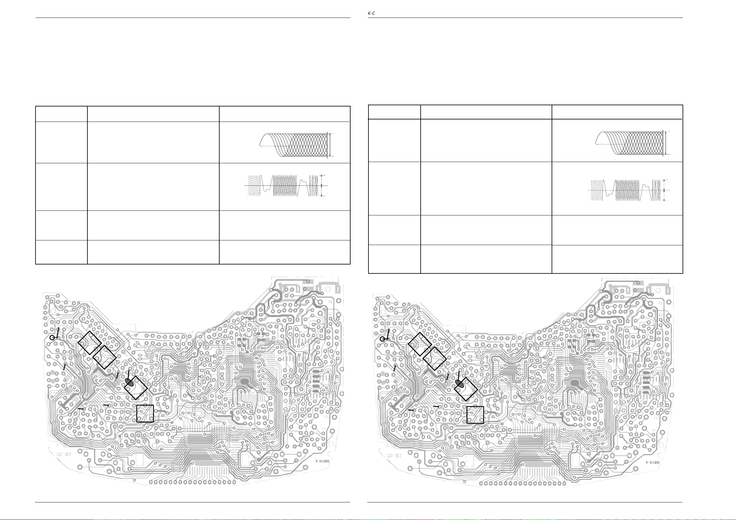
Abgleich
1. CD-Teil
Meßgeräte/Meßmittel:
Oszilloskop, NF-Voltmeter
Hinweise:
Verstellen Sie nicht den Regler für die Laserstromeinstellung! Der Laserstrom wurde werkseitig eingestellt.
Abgleich Vorbereitung Abgleichvorgang
1. Focus Offset
2. Tracking
EF Balance
3. Focus Servo
Gain
4. Tracking Servo
Gain
Oszilloskop an Meßpunkt TP4, Masse an TP3.
CD einlegen.
CD-Funktion: Play
Oszilloskop an Meßpunkt TP1, Masse an TP3.
Brücke JP1 auftrennen (Lötseite).
CD einlegen.
Die Messung ist nur möglich, solange das Gerät prüft,
ob eine CD eingelegt ist!
Brücke JP1 wieder schließen.
NF-Voltmeter an Meßpunkt TP2, Masse an TP3.
CD einlegen.
CD-Funktion: Play
NF-Voltmeter an Meßpunkt TP5, Masse an TP3.
CD einlegen.
CD-Funktion: Play-Track 1
Mit RV101 einen sauberen Kurvenverlauf (Augenmuster)
einstellen.
Mit RV102 Kurve symmetrisch zur 0-Linie (Vref)
einstellen.
Mit RV104 auf 90mV
Mit RV103 auf 31mV
einstellen.
eff
einstellen.
eff
0,5 µs/Div. 20mV/Div.
0,1 ms/Div. 20mV/Div. DC
V1
V2
V1 = V2
>1V
0
(Vref)
k
Alignment
1. CD-Section
Measuring instruments/equipment:
Oscilloscope, AF voltmeter
Notes:
Do not turn the variable resistor (laser power adjustment). The laser current is pre-set at the factory.
Adjustment Preparations Adjustment Processs
1. Focus Offset
Connect the oscilloscope to test point TP4, ground to
TP3.
Load a CD.
ss
2. Tracking
EF Balance
CD function: Play
Connect the oscilloscope to test point TP1, ground to
TP3.
Open the bridge JP1 (Solderside).
Load a CD.
The measure is only possible, as long as the CD - Player
checks the CD.
Close the bridge JP1.
3. Focus Servo
Gain
Connect the AF voltmeter to test point TP2, ground to
TP3.
Load a CD.
CD function: Play
4. Tracking Servo
Gain
Connect the AF voltmeter to test point TP5, ground to
TP3.
Load a CD.
CD function: Play - Track 1
Adjust RV101 to obtain a clear eye pattern as shown
in the diagram.
>1V
0.5 µs/Div. 20mV/Div.
Adjust RV102 so that the graph is symmetrical to the
0-line (Vref).
V1
V2
V1 = V2
Set 90 mV
Set 31mV
with RV104.
eff
with RV103.
eff
0.1 ms/Div. 20mV/Div. DC
pp
0
(Vref)
R102
TP3
TP4
RV101
RF Bias
TP5
TP2
RV102
EF Balance
JP1
TP1
RV103
Track Gain
RV104
Focus Gain
R102
TP3
TP4
RV101
RF Bias
TP5
TP2
RV102
EF Balance
JP1
TP1
RV103
Track Gain
RV104
Focus Gain
GRUNDIG Service 2-1
GRUNDIG Service 2-2
Page 8
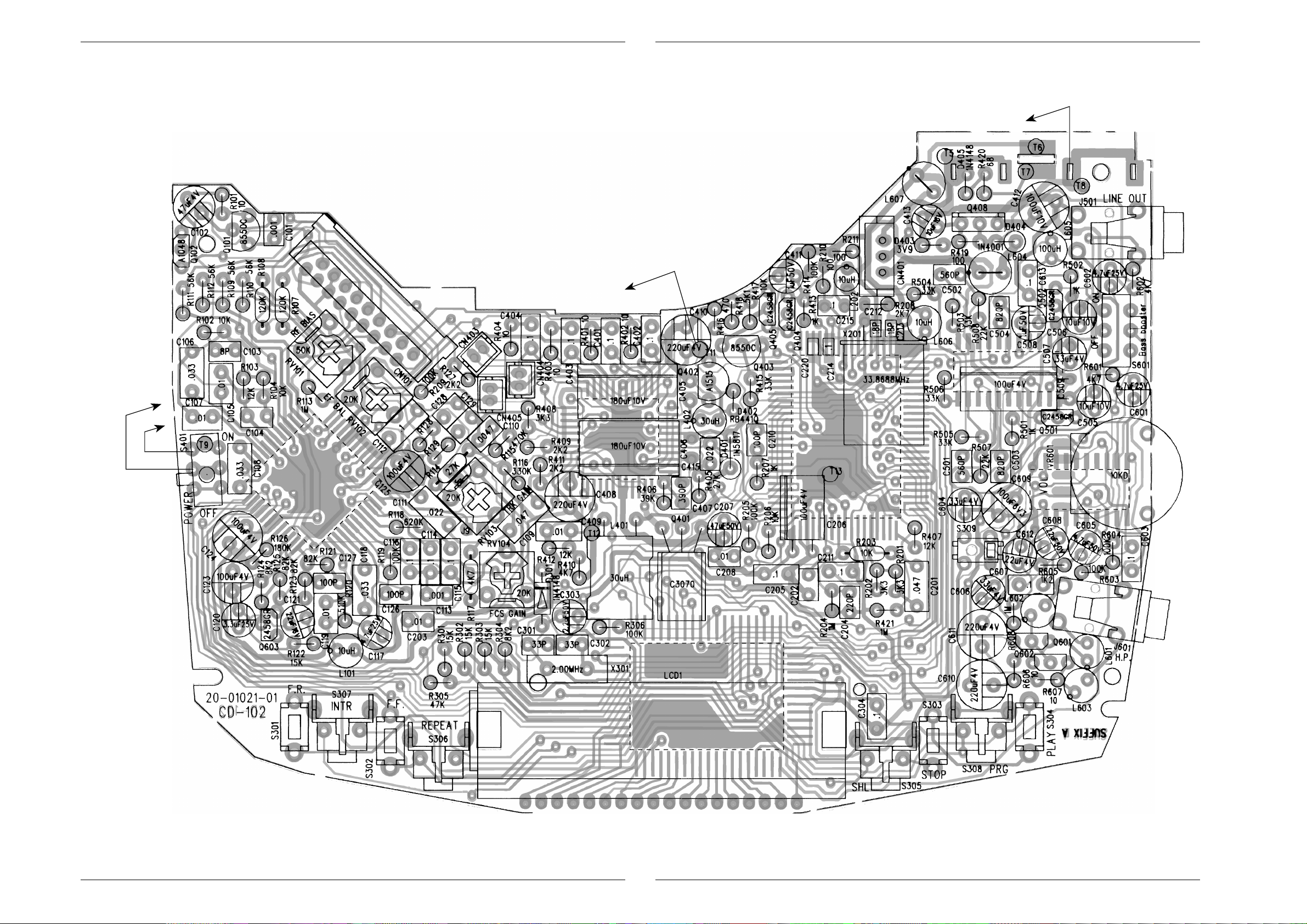
Platinenabbildung und Schaltplan / Layout of PCB and Circuit Diagram
Platinenabbildung und Schaltplan / Layout of PCB and Circuit Diagram
K-CDP 65
+´
Platinenabbildung und Schaltplan / Layout of PCB and Circuit Diagram
K-CDP 65
+
+
+´
25
24
36
U101
13
12
37
48
111
U501
22
12
34 44
33
65 80
64
1
1
U401
23
1
22
64
11
12
41
1
19
20
U201
24
2540
11 20
U601
110
3-1
52
GRUNDIG Service
3-2
U301
32
3351
GRUNDIG Service
Page 9
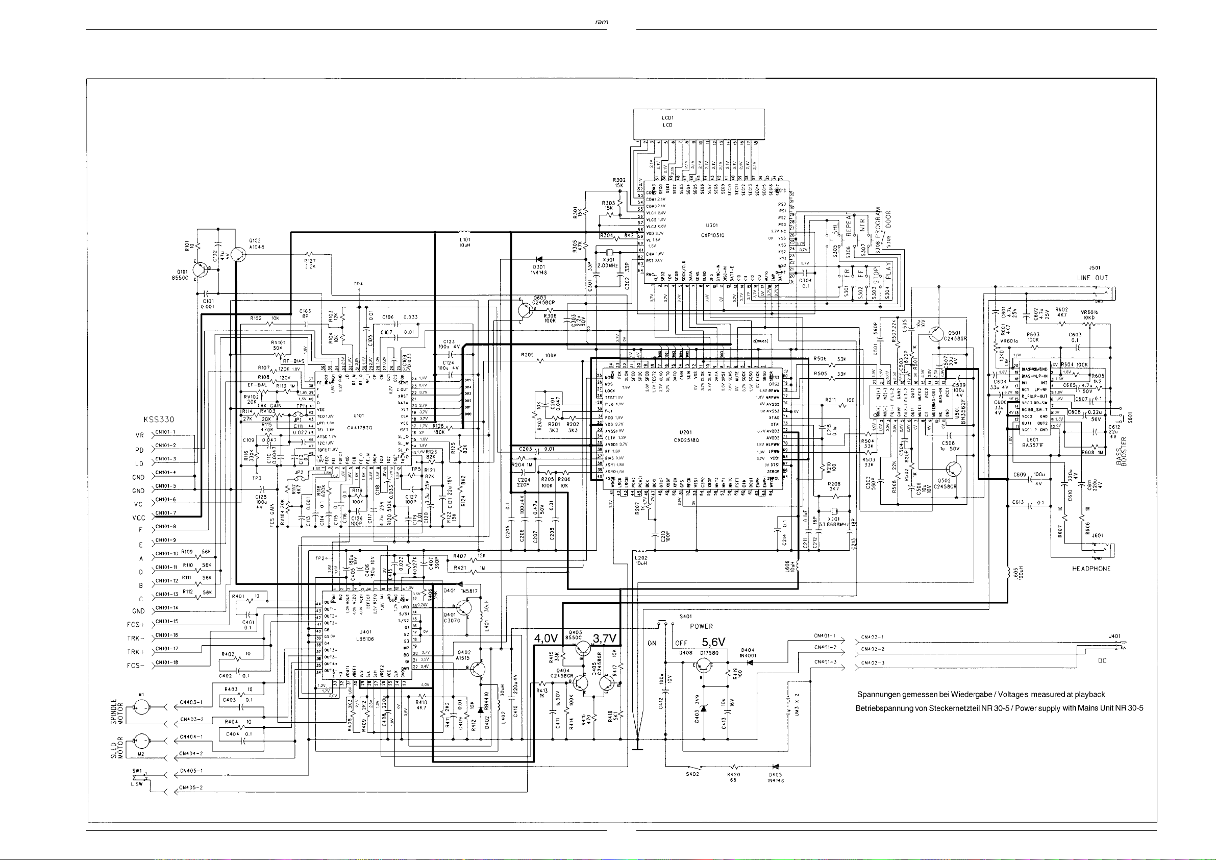
K-CDP 65K-CDP 65 Platinenabbildung und Schaltplan / Layout of PCB and Circuit DiagramPlatinenabbildung und Schaltplan / Layout of PCB and Circuit Diagram
3-43-3 GRUNDIG ServiceGRUNDIG Service
Page 10
Platinenabbildung und Schaltplan / Layout of PCB and Circuit Diagram K-CDP 65
Platinenabbildung und Schaltplan / Layout of PCB and Circuit Diagram K-CDP 65
ICs
U101 - CXA1782Q
Pin Name I /O Beschreibung
1 FEO I Focus error amplifier output. Connected internally to the FZC comparator input.
2 FEI I Focus error input
3 FDFCT I Capacitor connection pin for defect time constant.
4 FGD I Ground this pin through a capacitor when decreasing the focus servo high-frequency gain.
5 FLB I External time constant setting pin for increasing the focus servo low frequency.
6 FE_O O Focus drive output
7 FE_M I Focus amplifier negative input pin
8 SRCH I External time constant setting pin for generating focus servo waveform
9 TGU I External time constant setting pin for switching tracking high-frequency gain
10 TG2 I External time constant setting pin for switching tracking high-frequency gain
11 FSET I High cut off frequency setting pin for focus and tracking phase compensation amplifier
1 2 TA_M I Tracking amplifier negative input pin.
13 TA_O O Tracking drive output
14 SL_P I Sled amplifier non-inversed input.
15 SL_M I Sled amplifier negative input pin
16 SL_O O Sled drive output
17 ISET I Setting pin for focus search, Track jump and Sled kick current
18 VCC
1 9 CLK I Serial data transfer clock input from CPU (no pull up resistance)
2 0 XLT I Latch input from CPU (no pull up resistance)
2 1 DATA I Serial data input from CPU (no pull up resistance)
2 2 XRST I Reset input; reset at low. (no pull up resistance)
23 C OUT O Track number count signal output
24 SENS O Outputs FZC, DFCT, TZC, gain, balance, and other according to the command from CPU
25 FOK O Focus OK comperator output.
26 CC2 O Input pin for the DEFECT buttom hold output capacitance-coupled.
27 CC1 I DEFECT bottom hold output
28 CB I Connection pin for DEFECT bottom hold capacitor
2 9 CP I Connection pin for MIRR hold capacitor. MIRR comparator non-inversed input.
3 0 RF_I I Input pin for the RF summing amplifier output capacitance-coupled.
3 1 RF_O O RF summing amplifier output. Eye pattern check point.
32 RF_M I
3 3 LD O O APC amplifier output
3 4 PHD I APC amplifier input
35/36 PHD1/2 I RF I-V amplifier inversed input. Connect these pins to the photo diode A+C and B+D pins.
3 7 FE_Bias I Bias adjustment of focus error amplifier.
38/39 F/E I F I-V and E I-V amplifier inversed input. Connect these pins to photo diodes F and E.
40 EI I-V amplifier E gain adjustment. (When not using automatic balance adjustment)
41 VEE
4 2 TEO O Tracking error amplifier output.
43 LPFI I Comparator input for balance adjustment
4 4 TEI I Tracking error input
4 5 ATSC I Window comparator input for ATSC detection.
4 6 TZC I Tracking zero-cross comparator input.
47 TDFCT I Capacitor connection pin for defect time constant.
4 8 VC O (VCC+VEE)/2 DC voltage output.
RF summing amplifier inversed input.
The RF amplifier gain is determined by the resistance connected between this pin and RFO pin.
U101 - CXA1782Q
U601 - BA3571F
3-5 GRUNDIG Service
3-6 GRUNDIG Service
Page 11
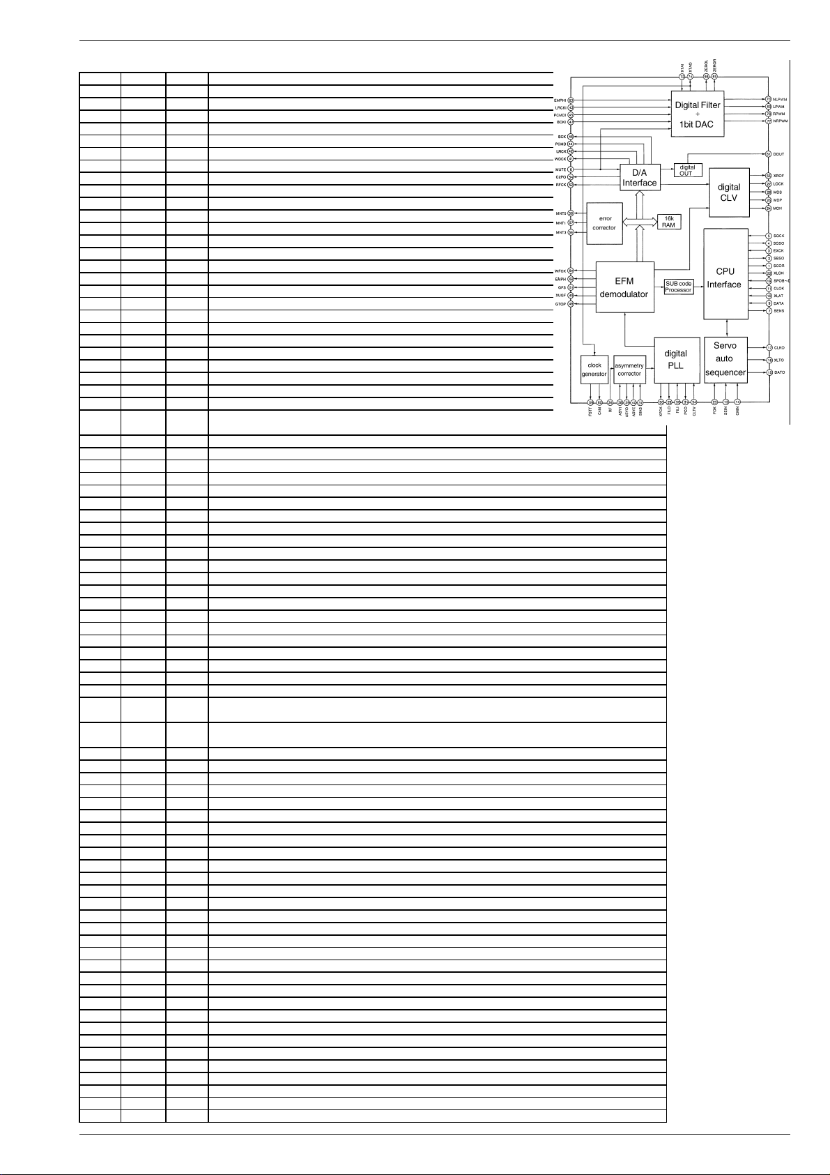
K-CDP 65 Platinenabbildung und Schaltplan / Layout of PCB and Circuit Diagram
U201 - CXD2518Q
Pin Name I/O Beschreibung
1 SCOR O Master PLL VCO control voltage input
2 SBSO O Analop power supply for DSP
3 EXCK I EFM signal input
4 SQSO O Constant current input of asymmerty compensation circuit
5 SQCK I Asymmetry compensation circuit comparator voltage input
6 MUTE I High: Mute; Low: release
7 SENS O SENS output to CPU
8 XRST I System reset. Reset when Low
9 DATA I Serial data input from CPU
10 XLAT I Latch input from CPU. Serial data is latched at the falling edge.
11 CLOK I Serial data transfer clock input from CPU
12 Vss GND
13 SEIN I Sense input from SSP
14 CNIN I Track jump count signal input
15 DATO O Serial data output to SSP
16 XLTO O Serial data latch output to SSP. Latched at the falling edge.
1 7 CLTO O Serial data transfer clock output to SSP.
18 TEST2 I Test pin; normally Vdd
19 SPOB I µC extended interface (input B).
20 SPOC I µC extended interface (input C).
21 SPOD I µC extended interface (input D).
22 XLON O µC extended interface (output).
23 FOK I Focus OK input. Used for SENS output and the servo auto sequencer.
24 MON O Spindle motor on/off control output.
25 MDP O Spindle motor servo control
26 MDS O Spindle motor servo control
27 LOCK O
GFS is sampled at 460 Hz; when GFS is high, this pin outputs a high signal.
If GFS is low eight consecutive samples, this pin outputs low.
28 TEST I Test pin. Normally GND.
29 FILO O Master PLL (slave = digital PLL) filter output
30 FILI I Master PLL filter input.
31 PCO O Master PLL charge pump output.
3 2 Vdd Digital power supply for DSP.
33 AVSS1 Analog GND for DSP.
34 CLTV I Master PLL VCO control voltage input.
35 AVDD1 Analog power supply for DSP.
36 RF I EFM signal input.
37 BIAS I Constant current input of asymmetry compensation circuit.
38 ASYI I Asymmetry compensation circuit comparator voltage input.
39 ASYO O EFM full-swing output (low = Vss, high = VdDD).
40 ASYE I compensation off; high: asymmetry compensation on.
41 WDCK O D/A interface for 48-bit slot. Word clock (2FS).
4 2 LRCK O D/A interface for 48-bit slot. LR clock (FS).
4 3 LRCKI I LR clock input for DAC. 48-bit slot)
44 PCMD O D/A interface. Serial data (two´s complement, MSB first)
45 PCMDI I Audio data input for DAC. (48-bit slot)
4 6 BCK O D/A interface. Bit clock.
47 BCKI I Bit clock input for DAC. (48-bit slot)
48 GTOP O GTOP output. Is used to monitor the frame sync protection status.(High: sync protection window off)
49 XUGF O
50 XPCK O
XUGF output. It ´s a negative pulse for the frame sync derived from the EFM signal.
It´s the signal before sync protection.
XPCK output. It´s the inverse of the EFM PLL clock.
The PLL is designed so that the falling edge and the EFM signal transition point coincide.
51 GFS O GFS output. It goes high when the frame sync and the insertion protection timing match.
52 RFCK O RFCK output.It´s derived from the crystal accuracy. This signal has a cycle of 136µ.
53 Vss GND
54 C2PO O C2PO output. It represents the data error status.
55 XROF O XRAOF output. It´s generated when the 16k RAM exceeds the ±4F jitter margin.
56 MNT3 O MNT3 output
57 MNT1 O MNT1 output
58 MNT0 O MNT0 output
59 FSTT O 2/3 frequency divider output for Pins 73 and 74.
60 C4M O 4.2336 MHz output.
61 DOUT O Digital OUT output
62 EMPH O Outputs high signal when the playback disc has emphasis, low signal when no emphasis.
6 3 EMPHI I DAC de-emphasis on/off. High: on; Low: off
64 WFCK O WFCK (write frame clock) output
65 ZEROL O No-sound data detection output; high when "no audio" data is detected (Left channel)
66 ZEROR O No-sound data detection output; high when "no audio" data is detected (Right channel)
6 7 DTSI I Test pin 1 for DAC; normally low.
6 8 VDD Digital power supply for DAC.
69 LPWM Left channel PWM output. (Forward phase)
70 NLPWM Left channel PWM output. (Reverse phase)
7 1 AVDD2 Power supply for left channel PWM driver.
7 2 AVDD3 Power supply for crystal.
73 XTAI 33.8688 MHz crystal oscillation circuit input.
74 XTAO 33.8688 MHz crystal oscillation circuit output.
75 AVSS3 GND for crystal.
76 AVSS2 GND for PWM driver
77 NRPWM Right channel PWM output. (Reverse phase)
78 RPWM Right channel PWM output. (Forward phase)
7 9 DTS2 DAC test pin 2; normally low.
8 0 DTS3 DAC test pin 3; normally low.
GRUNDIG Service 3-7
Page 12
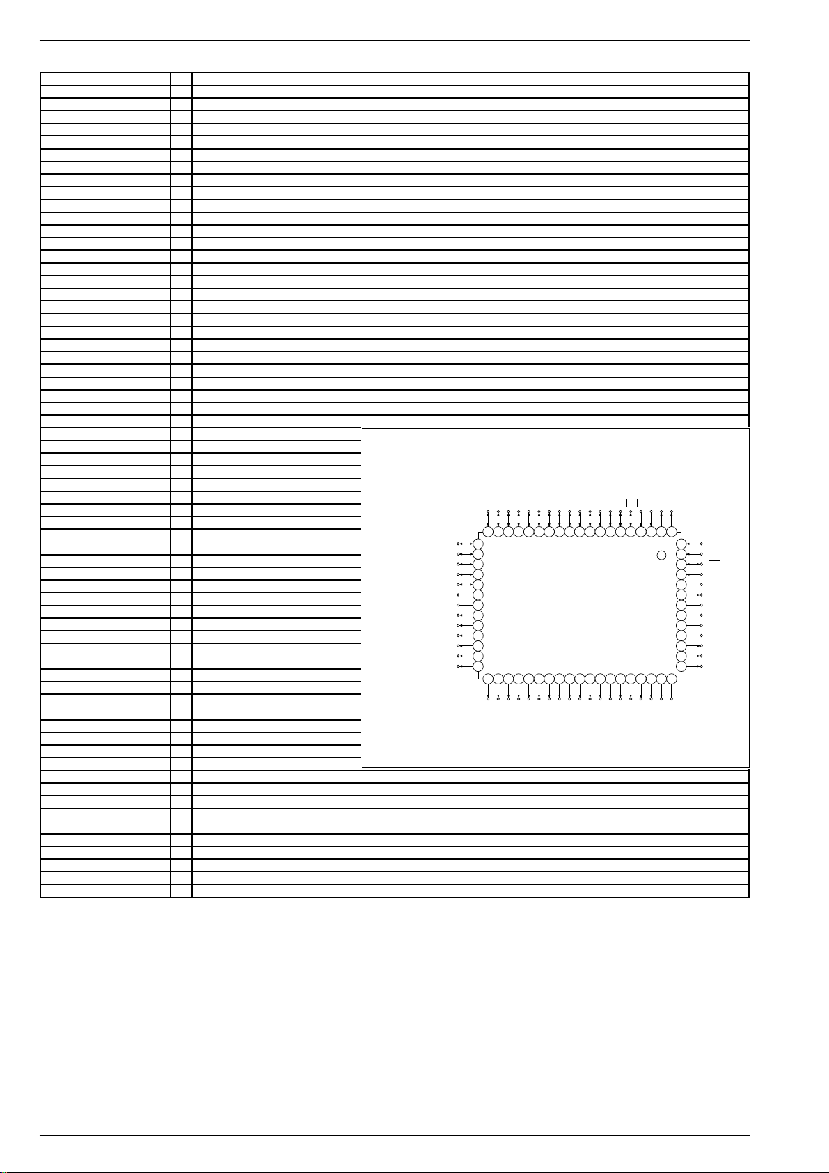
Platinenabbildung und Schaltplan / Layout of PCB and Circuit Diagram K-CDP 65
U301 - CXP1031Q
Pin Name I/O Beschreibung
1 XLT O Latch output
2 DRCTL O Motor driver select
3 FOK I Inputs focus conditions
4 SCOR I SCOR input
5 SQCK/CLK O SUB-Q reading clock output. 8-Bit data clock output
6 DATA O 8-Bit data output
7 SENSE I Sense input (monitor for various systems)
8 SUBQ I SUB-Q code input port
9 GFS I Monitor pin for the disc condition
10 SYNC IN I Used to operate CD synchronously with external equipment (cassette and others). Operates with falling edge.
11 DISC IN I Turn to "L" when tray has entered in deck mode and when the lid has closed in portable mode.
12 DISC OUT/BATT-E I Turn to "L" when tray has terminated open in deck mode and when there is no battery in portable mode.
13 KI0 I Port for key scan input. Reads remote control customer code at reset and start.
14 KI1 I Port for key scan input. Reads remote control customer code at reset and start.
15 KI2 I Port for key scan input. Reads remote control customer code at reset and start.
16 KI3 I Port for key scan input. Reads remote control customer code at reset and start.
17 MUTG O Mute ON at mute signal "H".
1 8 I key sel
19 UNLOAD/BATT-W IO In deck mode indicates tray loading motor operation output and in portable mode battery warning output
2 0 LOAD/DECK-PT IO Performs tray loading motor operation output in deck mode and portable mode branching at "L" detection just after Reset.
21 KS0 O Key scan output
22 KS1 O Key scan output
23 KS2 O Key scan output
24 KS3/TEST IO Performs test mode branching at "L" detection just after Reset.
25 VSS Connect to GND
26 NC Do not connect anything
2 7 RS3 O RMC customer code scan signal
2 8 RS2 O RMC customer code scan signal
2 9 RS1 O RMC customer code scan signal
3 0 RS0 O RMC customer code scan signal
31 - Not used
32 SEG18 O Connect to LCD
33 SEG17 O Connect to LCD
34 SEG16 O Connect to LCD
35 SEG15 O Connect to LCD
36 SEG14 O Connect to LCD
37 SEG13 O Connect to LCD
38 SEG12 O Connect to LCD
39 SEG11 O Connect to LCD
40 SEG10 O Connect to LCD
41 SEG9 O Connect to LCD
42 SEG8 O Connect to LCD
43 SEG7 O Connect to LCD
44 SEG6 O Connect to LCD
45 SEG5 O Connect to LCD
46 SEG4 O Connect to LCD
47 SEG3 O Connect to LCD
48 SEG2 O Connect to LCD
LOAD/DECK/PT/PB3
KS0/PA0
KS1/PA1
KS2/PA2
KS3/PA3
N.C.
RS3/PE3
RS2/PE2
RS1/PE1
RS0/PE0
SEG19
SEG18
V
SS
OPB2/UNLOAD/Batt-W
OPB1/EMPHAISI
OPB0/MUTG
20
21
22
23
24
25
26
27
28
29
30
31
32
PC3/K13
PC2/K12
PC1/K11
PC0/K10
PD3/Disc OUT/Batt-E
PD2/Disk IN
PD1/SYNC IN
PD0/GFS
SI/SUBQ
PX2/SENSE
SOB/DATA
SC/SOCK/CLK
EC/SCOR
PY2/FOK
PY1/DRCTL
51504948474645444342414039383736353433
PY0/XLT
12345678910111213141516171819
64
INTI
63
WP
62
RST
61
EXTAL
60
XTAL
59
V
L
58
V
00
57
V
LC3
56
V
LC2
55
V
LC1
54
COM0
53
COM1
52
COM2
49 SEG1 O Connect to LCD
50 SEG0 O Connect to LCD
51 COM3 O Connect to LCD
SEG17
SEG16
SEG15
SEG14
SEG13
SEG12
SEG9
SEG8
SEG7
SEG6
SEG5
SEG4
SEG3
SEG2
SEG1
SEG0
SEG11
SEG10
COM3
52 COM2 O Connect to LCD
53 COM1 O Connect to LCD
54 COM0 O Connect to LCD
55 VLC1 Supply pin for LCD bias power supply
56 VLC2 Supply pin for LCD bias power supply
57 VLC3 Supply pin for LCD bias power supply
58 VDD VDD
59 VL O Supply pin for LCD bias power supply
60 XTAL Connect CRYSTAL
61 EXTAL I Connect the clock
62 RESET IO Connect RESET
63 WP I Not used
64 RMC I Connect to remote control input and remote control module
3-8 GRUNDIG Service
Page 13
K-CDP 65 Platinenabbildung und Schaltplan / Layout of PCB and Circuit Diagram
U401 - LB8106
Pin Name Beschreibung
1 IN1 Focus actuator control input
2 IN2 Tracking actuator control input
3 VOUT Bridge driver outputs
4 VCD2 UP converter input
5 VCD1 UP converter input
6 DEFECT Defect input
7 REFO Sled drive reference voltage output
8 IAI Integrating amplifier input
9 AO Inverting amplifier output
10 IAO Integrating amplifier output
1 1 OSC Oscillator input
12 OSCPOW Oscillator supply output
1 3 UPB UP converter npn-transistor driver output
14 SS1 System startup input 1
15 SS2 System startup input 2
16 FGND Frame ground
17 FGND Frame ground
18 FGND Frame ground
19 WP Microcomputer startup output
20 BO Battery check output
21 BI Battery check input
2 2 DNB Down converter pnp-transistor driver output
23 GND Signal ground
2 4 CLK Clock input
25 VCC 2.4V supply
26 VREF2 1.2V reference voltage
27 SLH Sled driver startup voltage adjustment input
28 SLL Sled driver stop voltage adjustment input
29 SL S Sled changeover input
30 VREF1 Actuator driver reference voltage input
31 VOUT Bridge driver outputs
32 IN3 Spindle actuator control input
33 IN4 Sled actuator control input
34 OUT4- Negative sled actuator driver output
35 OUT4+ Positive sled actuator driver output
36 OUT3- Negative spindle actuator driver output
37 OUT3+ Positive spindle actuator driver output
38 FGND Frame ground
39 FGND Frame ground
40 FGND Frame ground
41 OUT2- Negative tracking actuator driver output
42 OUT2+ Positive tracking actuator driver output
43 OUT1- Negative focus actuator driver output
44 OUT1+ Positive focus actuator driver output
IN1
IN2
VOUT
VCD2
VCD1
DEFECT
REFO
IAI
AO
IAO
OSC
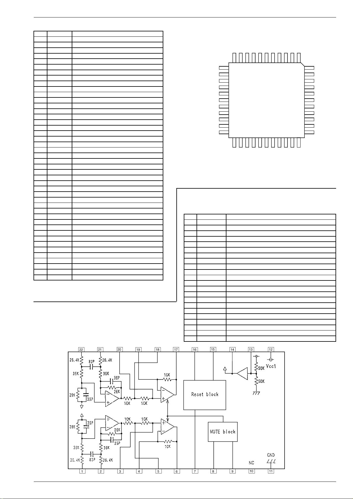
U501 BH3562
Pin Name Beschreibung
1 IN1+ CH1 positive input
2 IN1- CH1 negative input
3 FILTER 1-1 Pin 1-1 for setting filter
4 GAIN1 Pin 1 for changing gain
5 FILTER 2-1 Pin 2-1 for setting filter
6 OUT1 CH1 output
7 OUTMUTE1 CH1 MUTE Tr driving pin
8 CT Capacitor connecting pin for setting constant at MUTE
9 MUTE MUTE control pin
10 N.C.
11 GND GND
1 2 VCC1 Power supply
13 BIAS IN BIAS input pin
14 BIAS OUT Bias output pin
1 5 VCC2 Power supply for reset block idling
16 OUTMUTE 2 CH2 Output MUTE Tr driving pin
1 7 OUT2 CH2 output
1 8 FILTER 2-2 Pin 2-2 for setting filter
19 GAIN2 Pin 2 for changing gain
2 0 FILTER 1-2 Pin 1-2 for setting filter
21 IN2- CH2 negative input
22 IN2+ CH2 positive input
OUT1+
OUT1-
OUT2+
OUT2-
FGND
FGND
FGND
OUT3+
1
LB8106
11
12 22
SS1
UPB
OSCPOW
SS2
FGND
FGND
FGND
WP
OUT3-
OUT4+
BI
BO
OUT4-
3444
33
23
DNB
IN4
IN3
VOUT
VREF1
SLS
SLL
SLH
VREF2
VCC
CLK
GND
GRUNDIG Service 3-9
Page 14
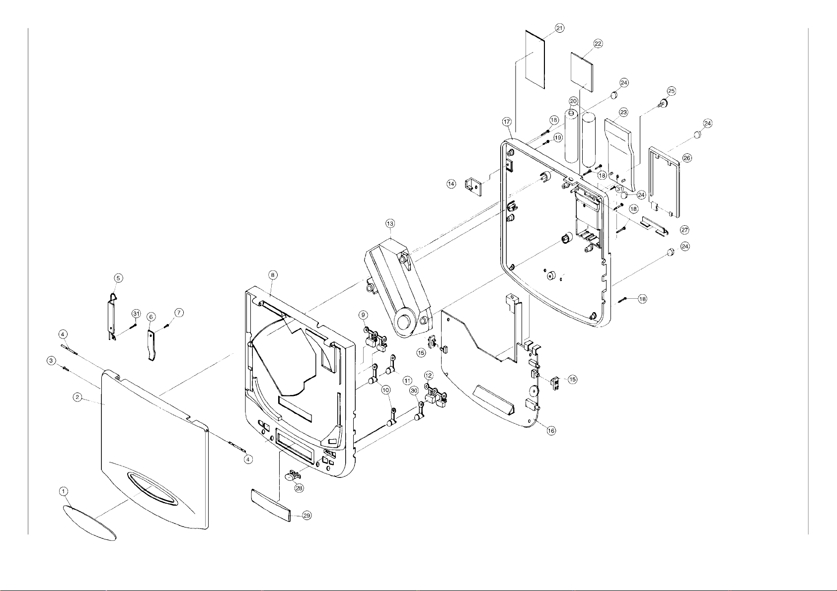
4-1
Explosionszeichnung und Ersatzteilliste / Exploded View and Spare Parts List
Explosionszeichnung / Exploded View
Explosionszeichnung und Ersatzteilliste / Exploded View and Spare Parts List
GRUNDIG Service
K-CDP 65
Page 15
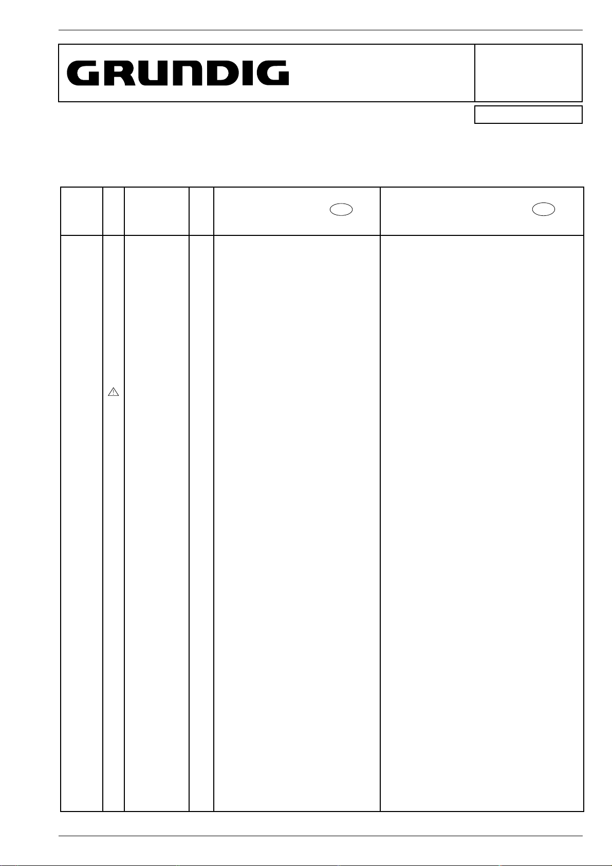
K-CDP 65 Ersatzteilliste / Spare Parts List
Ersatzteilliste
Spare Parts List
5 / 95 K-CDP 65
SACH-NR. / PART NO.: 75.5073-1051
BESTELL-NR. / ORDER NO.: G.DF 9051
POS. ABB. SACHNUMMER ANZ.
NR. NR.
POS. FIG. PART NUMBER QUA.
NO. NO.
0001.000 1 75954-020.31 CD-LINSE CD-LENS
0002.000 1 75954-020.28 CD DECKEL CD-COVER
0008.000 1 75954-020.26 GEHAEUSE OBERTEIL HOUSING TOP CABINET
0013.000 1 75954-020.34 CD-LAUFWERK CD-TAPE DRIVE
0015.000 1 75954-020.43 SCHIEBE KNOPF SLIDE KNOB
0017.000 1 75954-020.27 GEHAEUSE BODEN HOUSING BOTTOM CABINET
0024.000 1 75954-020.33 GUMMI-STANDFUSS RUBBER FOOT STAND
0026.000 1 75954-020.30 BATTERIEDECKEL BATTERY LID
0027.000 1 75954-020.35 BATTERIE KONTAKTPLATTE BATTERY CONTACT BOARD
0028.000 1 75954-020.29 KNOPF CD-DECKEL OEFFNEN KNOB CD-COVER OPEN
0029.000 1 75954-020.32 DISPLAY LINSE DISPLAY LENS
0033.000 75954-020.36 BATTERIE FEDER + BATTERY SPRING +
0034.000 75954-020.37 BATTERIE FEDER - BATTERY SPRING -
0040.000 75954-020.38 OHR-HOERER WB-1A STEREO EAXPHONE
0041.000 75954-020.39 NETZTEIL NR30-5 POWER SUPPLY
BEZEICHNUNG
D
DESCRIPTION
GB
72010-743.15 BEDIENUNGSANLEITUNG 10SPR INSTRUCTION MANUAL
72010-743.90 SERVICE MANUAL D/GB SERVICE MANUAL D/GB
ÄNDERUNGEN VORBEHALTEN SUBJECT TO ALTERATION
GRUNDIG Service 4-2
Page 16
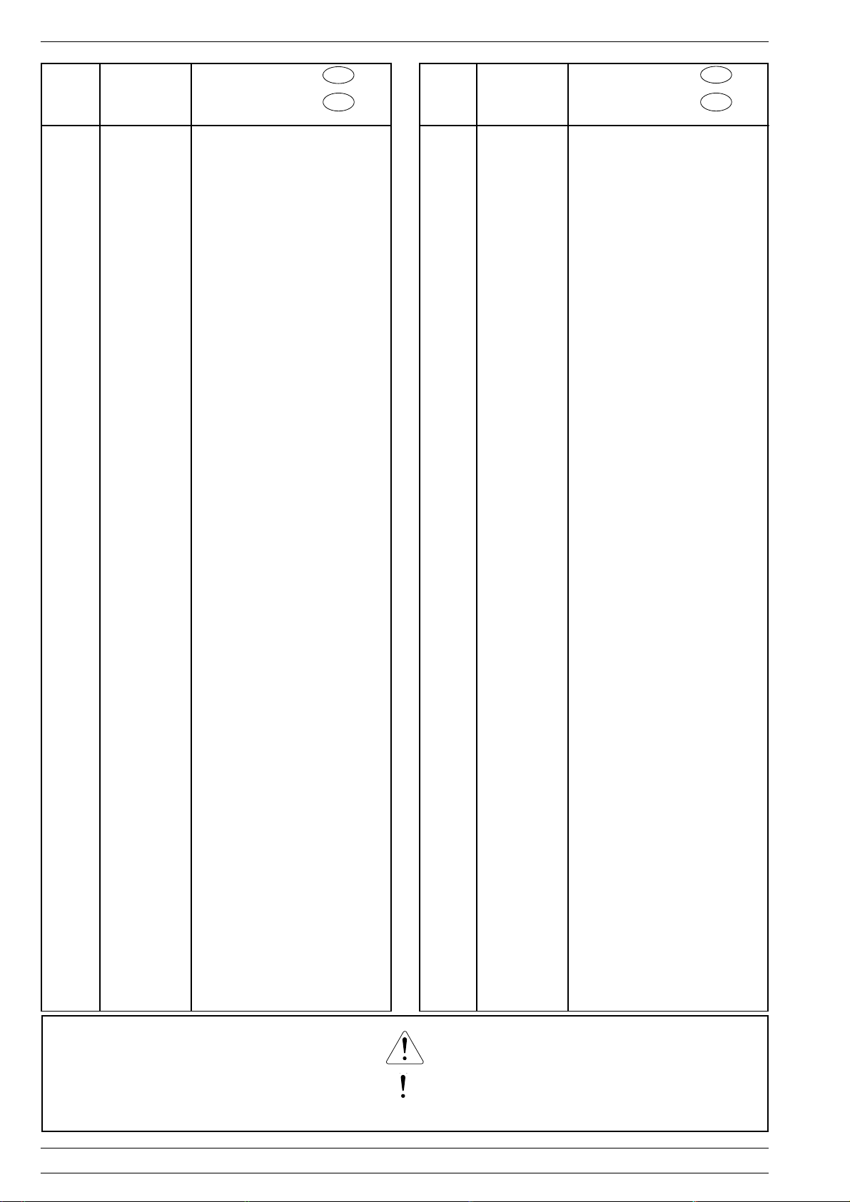
Ersatzteilliste / Spare Parts List K-CDP 65
POS.
NR.
POS.
NO.
D 301 8309-215-050 DIODE 1 N 4148
D 401 8309-215-817 DIODE 1 N 5817 -GA PHI
D 402 75954-020.21 DIODE RB 441 Q
D 403 8309-707-055 Z DIODE ZPD 3,9 2% ITT
D 404 75954-020.22 DIODE RL 202
D 405 8309-215-050 DIODE 1 N 4148
IC 101 75954-020.11 IC CXA 1782 BQ
IC 201 75954-020.12 IC CXD 2518 Q
IC 301 75954-020.10 IC CXP 10310Q
IC 401 75950-022.22 IC LB 8106 M
IC 501 75954-020.13 IC BA 3562 F
IC 601 75954-020.14 IC BA 3571 F
J 1 75954-020.02 BUCHSE STROMVESORGUNG
J 501 75954-020.01 KOPFHOERER BUCHSE
J 601 75954-020.40 CINCH-BUCHSE LIN-OUT
L 101 75954-020.15 SPULE 1 UH RL4055 100K10%
L 202 75954-020.15 SPULE 1 UH RL4055 100K10%
L 401 75954-020.18 SPULE 30UH RL8080 300K
L 402 75954-020.17 SPULE 30UH RL4055 300K
L 605 75954-020.16 SPULE 100UH RL3040 101K
L 606 75954-020.15 SPULE 1 UH RL4055 100K10%
SACHNUMMER
PART NUMBER
BEZEICHNUNG
DESCRIPTION
D
GB
POS.
NR.
POS.
NO.
S 601 75954-020.03 SCHIEBESCHALTER
X 201 75954-020.24 QUARZ 33.8688MHZ
X 301 75954-020.25 KERAMIK SCHWINGER CSA2.00
SACHNUMMER
PART NUMBER
BEZEICHNUNG
DESCRIPTION
D
GB
LCD 1 75954-020.23 LCD ANZEIGE TCM 358
Q 101 75954-020.09 TRANS. SS8550 C
Q 102 75952-701.76 TRANS.2 SA 1048 GR
Q 401 75954-020.07 TRANS.2 SD 2172
Q 402 75954-020.08 TRANS. 2SA 1515 Q
Q 403 75954-020.09 TRANS. SS8550 C
Q 404 75985-600.47 TRANS.2 SC 2458 GR
Q 405 75985-600.47 TRANS.2 SC 2458 GR
Q 408 75954-020.42 TRANS. 2SD 1758 Q
Q 501 75985-600.47 TRANS.2 SC 2458 GR
Q 502 75985-600.47 TRANS.2 SC 2458 GR
Q 603 75985-600.47 TRANS.2 SC 2458 GR
RV 1 75954-020.41 REGLER 10K
RV 101 75954-020.20 REGLER KVSF637AB 50KOHM
RV 102 75954-020.19 REGLER KVSF637AB 20KOHM
RV 103 75954-020.19 REGLER KVSF637AB 20KOHM
RV 104 75954-020.19 REGLER KVSF637AB 20KOHM
S 301 75954-020.06 TAKT-SCHALTER
S 302 75954-020.06 TAKT-SCHALTER
S 303 75954-020.06 TAKT-SCHALTER
S 304 75954-020.06 TAKT-SCHALTER
S 305 75954-020.05 TAKT SCHALTER
S 306 75954-020.05 TAKT SCHALTER
S 307 75954-020.05 TAKT SCHALTER
S 308 75954-020.05 TAKT SCHALTER
S 309 75954-020.04 TAKT-SCHALTER
S 401 75954-020.03 SCHIEBESCHALTER
Es gelten die Vorschriften und Sicherheitshinweise gemäß dem Service Manual "Sicherheit",
Sach-Nummer 72010-800.00, sowie zusätzlich
die eventuell abweichenden, landesspezifischen
( )
The regulations and safety instructions shall be
valid as provided by the "Safety" Service Manual,
part number 72010-800.00, as well as the
respective national deviations.
Vorschriften!
Änderungen vorbehalten Printed in Germany Service Manual Sach-Nr. 72010-743.90
Subject to alteration VK 23 0595 Service Manual Part No. 72010-743.90
 Loading...