

Page 1
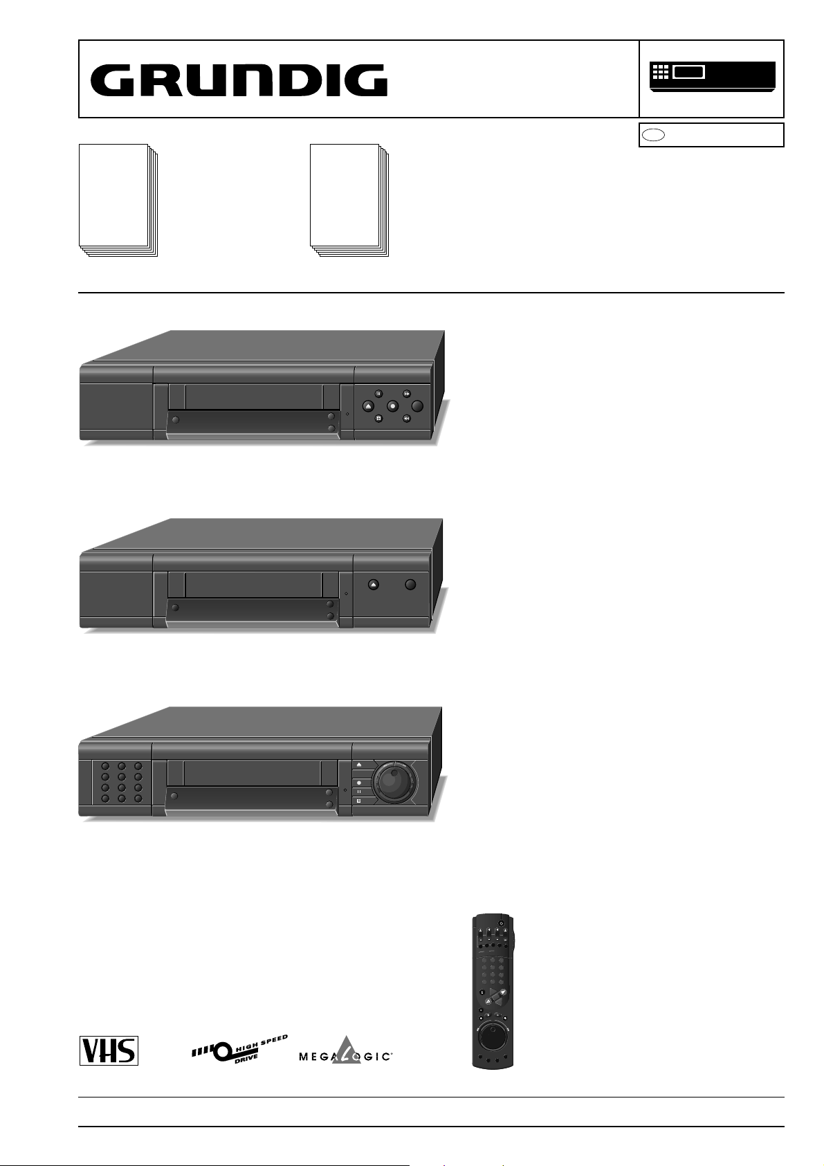
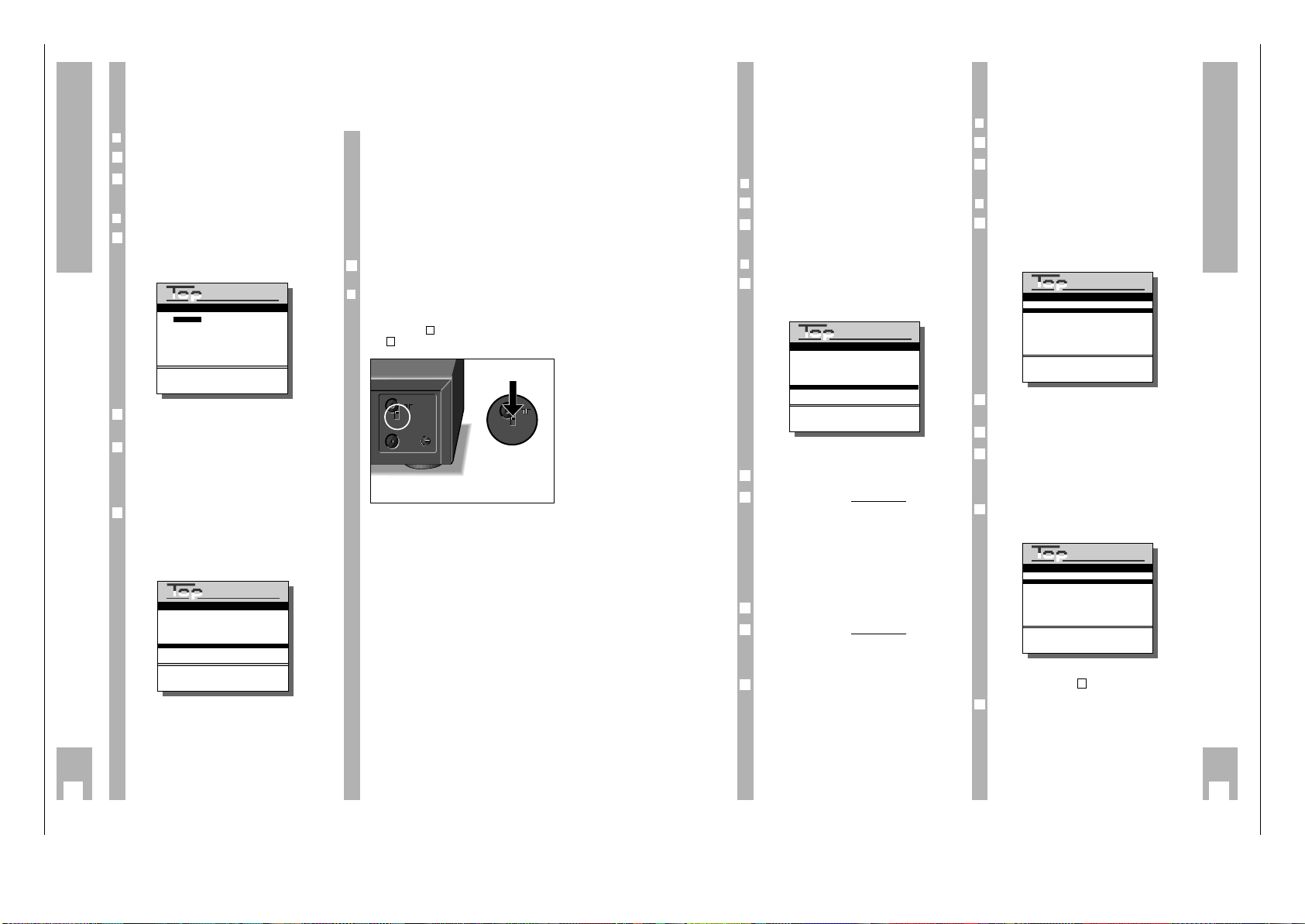
Service
Manual
GV 54…
GV 56…
SE 5106 …
Sach-Nr./Part No.
72010-519.45
Zusätzlich erforderliche Unterlagen
für den
Komplettservice:
Additionally required
Service Manuals for
the Complete Service:
TIMER
ON/OFF
Service
Manual
Sicherheit
Safety
Sach-Nr./Part No.
72010-800.00
%
%
SERVICE MANUAL
GV 5695 … / Madrid
GV 540 GB (77400-617.51 / G.ME 3300 GB)
GV 540 HIFI (77400-603.51 / G.ME 3000)
GV 540 NIC (77400-608.51 / G.ME 3100)
e
VIDEO
D
Btx * 32700
#
GV 540 …
GV 560 …
SE 5106 …
(77400-659.51 / G.ME 3110)
1 2 3
4 5 6
7 8 9
SV
0
GV 560 HIFI (77400-601.51 / G.ME 3600)
GV 560 HIFI/LE (77400-661.51 / G.ME 6300)
GV 560 NIC (77400-609.51 / G.ME 3700)
(77400-662.51 / G.ME 3710)
ON/OFF
e
TIMER
%
%
GV 5695 HIFI / Madrid (77400-642.51 / G.ME 3900)
SE 5106 HIFI (77400-638.51 / G.ME 2700)
e
TIMER
AV
ON / OFF
%
%
DAY START
STOP
PROG.
ON/OFF
SP/LP
CLEAR
SV/V+
SET/CHECK
TIMER
2
3
1
5
6
4
8
9
7
0
AVVPT
RP540 (75988-010.73)
+
+
OK
-
I
G
N
N
D
I
K
E
C
X
A
R
T
I
N
D
E
E
S
X
A
M
R
E
A
X
R
K
D
E
I
N
PAL / SECAM OST
Änderungen vorbehalten Printed in Germany Service Manual Sach-Nr.
Subject to alteration VK 21/1 0895 Service Manual Part No. 72010-519.45
Page 2

Allgemeiner Teil / General GV 54…, GV 56…, SE 5106…
Es gelten die Vorschriften und Sicherheitshinweise
gemäß dem Service Manual "Sicherheit", Sach-Nummer 72010-800.00, sowie zusätzlich die eventuell
abweichenden, landesspezifischen Vorschriften!
D
Inhaltsverzeichnis
Seite
Allgemeiner Teil................................... 1-1…1-30
Geräteübersicht .................................................................................. 1-3
Meßgeräte / Meßmittel........................................................................ 1-5
Technische Daten ............................................................................... 1-5
Bedienelemente .................................................................................. 1-6
Servicehinweise ................................................................................ 1-22
Servicetestprogramm und Sonderfunktionen.................................... 1-27
Beschreibungen.................................... 2-1…2-22
Netzteil (OSM / PS)............................................................................. 2-1
Chassisplatte (OFBG)......................................................................... 2-3
• Ablaufsteuerung (CC) ...................................................................... 2-3
• Empfangseinheit (FE) ...................................................................... 2-6
• IN/OUT (IO)...................................................................................... 2-7
• Audio (AU) ....................................................................................... 2-8
• OSD-Baustein (OOSDG / OS) ....................................................... 2-10
Chassisplatte II (OKV++G) ............................................................... 2-11
• Laufwerksteuerung / Deck-Elektronik (DE) .................................... 2-11
• Video/Chroma (VS) ........................................................................ 2-13
• Kopfverstärker (HC) ....................................................................... 2-16
Teletext-Baustein "DOS" (OVPTG / VT) ........................................... 2-17
NICAM-Decoder (ONI / NI) ............................................................... 2-18
"Edit Control"-Baustein (OLBG / EC) ................................................ 2-19
Bedieneinheiten (ODCG / DC) .......................................................... 2-20
Abgleich .................................................. 3-1…3-4
Netzteil (OSM / PS)............................................................................. 3-1
Chassisplatte (OFBG)......................................................................... 3-1
• Ablaufsteuerung (CC) ...................................................................... 3-1
• Empfangseinheit (FE) ...................................................................... 3-2
• IN/OUT (IO)...................................................................................... 3-2
• Audio (AU) ....................................................................................... 3-3
• OSD-Baustein (OOSDG / OS) ......................................................... 3-3
Chassisplatte II (OKV++G) ................................................................. 3-4
• Video/Chroma (VS) .......................................................................... 3-4
Teletext-Baustein "DOS" (OVPTG / VT) ............................................. 3-4
Platinenabbildungen
und Schaltpläne ................................... 4-1…4-96
Hinweise zu den Bauteilen / Schaltplansymbole ................................ 4-1
Verdrahtungspläne.............................................................................. 4-7
Blockschaltpläne (Netzteil, Digital, Video/Chroma, Audio) ............... 4-19
Netzteil (OSM / PS)........................................................................... 4-27
Chassisplatte (OFBG)....................................................................... 4-31
• Ablaufsteuerung (CC) .................................................................... 4-35
• VPS (VP)........................................................................................ 4-38
• Empfangseinheit (FE) .................................................................... 4-39
• IN/OUT (IO).................................................................................... 4-43
• Audio (AU) ..................................................................................... 4-46
• OSD-Baustein (OOSDG / OS) ....................................................... 4-49
"Edit Control"-Baustein (OLBG / EC) ................................................ 4-51
Laufwerkplatte – Sensoreneinheit..................................................... 4-59
Chassisplatte II (OKV++G) ............................................................... 4-53
• Laufwerksteuerung / Deck-Elektronik (DE) .................................... 4-61
• Video/Chroma (VS) ........................................................................ 4-65
• Kopfverstärker (HC) ....................................................................... 4-69
Teletext-Baustein "DOS" (OVPTG / VT) ........................................... 4-71
NICAM-Decoder (ONI / NI) ............................................................... 4-74
Bedieneinheiten (ODCG / DC) .......................................................... 4-77
Oszillogramme .................................................................................. 4-93
Laufwerk .............................................. 5-1…5-12
Meßgeräte / Meßmittel........................................................................ 5-1
Servicehinweise .................................................................................. 5-2
Auswechseln von Laufwerksteilen ...................................................... 5-3
Einstellungen .................................................................................... 5-10
Explosionszeichnungen
und Ersatzteilliste ............................... E-1…E-43
The regulations and safety instructions shall be valid
as provided by the "Safety" Service Manual, part
number 72010-800.00, as well as the respective
national deviations.
GB
Table of Contents
Page
General ................................................. 1-1…1-30
Video Recorder Overview ................................................................... 1-3
Test Equipment / Aids......................................................................... 1-5
Specifications ...................................................................................... 1-5
Operating Elements .......................................................................... 1-14
Service Instructions........................................................................... 1-22
Service Test Programme and Special Functions.............................. 1-27
Descriptions.......................................... 2-1…2-22
Power Supply (OSM / PS) .................................................................. 2-1
Family Board (OFBG) ......................................................................... 2-3
• Sequence Control (CC) ................................................................... 2-3
• Frontend (FE)................................................................................... 2-6
• IN/OUT (IO)...................................................................................... 2-7
• Audio (AU) ....................................................................................... 2-8
• OSD Module (OOSDG / OS) ......................................................... 2-10
Family Board II (OKV++G) ................................................................ 2-11
• Drive Control / Deck Electronic (DE).............................................. 2-11
• Video/Chroma (VS) ........................................................................ 2-13
• Head Amplifier (HC) ....................................................................... 2-16
Teletext Modul "DOS" (OVPTG / VT) ............................................... 2-17
NICAM-Decoder (ONI / NI) .............................................................. 2-18
Edit Control Modul (OLBG / EC) ....................................................... 2-19
Keyboard Control Units (ODCG / DC) .............................................. 2-20
Adjustment Procedures......................... 3-5…3-8
Power Supply (OSM / PS) .................................................................. 3-5
Family Board (OFBG) ......................................................................... 3-5
• Sequence Control (CC) ................................................................... 3-5
• Frontend (FE)................................................................................... 3-6
• IN/OUT (IO)...................................................................................... 3-6
• Audio (AU) ....................................................................................... 3-7
• OSD Module (OOSDG / OS) ........................................................... 3-7
Family Board II (OKV++G) .................................................................. 3-8
• Video/Chroma (VS) .......................................................................... 3-8
Teletext Modul "DOS" (OVPTG / VT) ................................................. 3-8
Layout of the PCBs
and Circuit Diagrams.......................... 4-1…4-96
Note on the Components / Circuit Diagram Symbols ......................... 4-1
Wiring Diagrams ................................................................................. 4-7
Block Circuit Diagrams (Power Supply, Digital, Video/Chroma, Audio) ..... 4-19
Power Supply (OSM / PS) ................................................................ 4-27
Family Board (OFBG) ....................................................................... 4-31
• Sequence Control (CC) ................................................................. 4-35
• VPS (VP)........................................................................................ 4-38
• Frontend (FE)................................................................................. 4-39
• IN/OUT (IO).................................................................................... 4-43
• Audio (AU) ..................................................................................... 4-46
• OSD Module (OOSDG / OS) ......................................................... 4-49
Edit Control Module (OLBG / EC) ..................................................... 4-51
Tape Deck Sensor Panel .................................................................. 4-59
Family Board II (OKV++G) ................................................................ 4-53
• Drive Control / Deck Electronic (DE).............................................. 4-61
• Video/Chroma (VS) ........................................................................ 4-65
• Head Amplifier (HC) ....................................................................... 4-69
Teletext Module "DOS" (OVPTG / VT) ............................................. 4-71
NICAM-Decoder (ONI / NI) ............................................................... 4-74
Keyboard Control Units (ODCG / DC) .............................................. 4-77
Oscillograms ..................................................................................... 4-93
Drive Mechanism................................. 5-1…5-12
Test Equipment / Aids......................................................................... 5-1
Service Instructions............................................................................. 5-2
Replacement of Tape Deck Components ........................................... 5-3
Adjustments ...................................................................................... 5-10
Exploded Views and
Spare Parts List .................................. E-1…E-43
1 - 2 GRUNDIG Service
Page 3
GV 54 …, GV 56 …, SE 5106… Allgemeiner Teil / General
Allgemeiner Teil / General
Geräteübersicht / Video Recorder Overview
GV 54 …, GV 56 …, SE 5106… Allgemeiner Teil / General
S./P 4-59Laufwerkplatte-Sensoreneinheit / Tape Deck Sensor Panel75988-001.18
S./P 4-27Netzteil / Power Supply (OSM / PS)27599-003.14
S./P 4-31
Chassisplatte / Family Board (OFBG)
Bausteinübersicht
Table of Moduls
S./P 4-53
S./P 4-61
S./P 4-35
S./P 4-39
S./P 4-43
S./P 4-46
S./P 4-38
S./P 4-49
· Ablaufsteuerung / Sequence control (CC)
· Empfangseinheit / Frontend (FE)
· IN/OUT (IO)
· Audio (AU)
· VPS (VP)
· OSD (OOSDG / OS)
S./P 4-65
Chassisplatte II / Family Board II (OKV++G)
· Laufwerkssteuerung / Deck-Elektronik (DE)
· Video/Chroma (VS)
S./P 4-51"Edit Control"-Baustein / Module (OLBG / EC)27599-032.16
S./P 4-69
· Kopfverstärker / Head Amplifier (HC)
S./P 4-77Bedieneinheit I / Keyboard Control Unit I (ODCG7 / DC)27599-002.50
S./P 4-74NICAM-Decoder (ONI / NI)27599-006.01
S./P 4-71Teletext-Baustein / Module "DOS" (OVPTG / VT)27599-009.00
S./P 4-82Bedieneinheit II / Keyboard Control Unit II (ODCG81 / DC)–
S./P 4-83Bedieneinheit I / Keyboard Control Unit I (ODCG8 / DC)27599-002.48
S./P 4-81Bedieneinheit II / Keyboard Control Unit II (ODCG71 / DC)75988-031.84
Feature-Übersicht
Table of Features
S./P 4-88Bedieneinheit I / Keyboard Control Unit I (ODCG6 / DC)27599-002.51
GV 540 GB
GV 540 HIFI
GV 540 NIC
GV 560 HIFI
GV 560 HIFI/LE
GV 560 NIC
GV 5695 HIFI
SE 5106 HIFI
27599-001.77
• • •
• • •
• •••••••
• •••••••
•
• •
•••
• •
•
• •••
•••
• • •
•••
•••••
•••
CCIR, BG - SECAM
CCIR, B/G/H - PAL
• • •••
•••••••
NICAM
CCIR, I - PAL
• • •
•
S-VHS-Wiedergabe / S-VHS Playback
NTSC-Wiedergabe / NTSC Playback
• •••••••
• •••••••
HiFi-Stereo
6 Kopf / Head (4Video, 2Audio)
• •••••••
• •••••••
Energiesparend / Low Power
Normalplay / Longplay (Video / Audio)
• •••••••
• •••••••
Megalogic
• •••••••
• •••••••
Follow TV
• •••••••
VPS
PDC
• •••••••
6 Timer
• •••••••
SHOW VIEW
•••••••
99 Programme, EURO-AV1, EURO-AV2/PAY-TV
VIDEO +
• •••••••
•
OSD
Teletext "DOS"
• • •
•••••
Kindersicherung / child lock
Titelgenerator / Title Generator
• •••••••
•••••
Insert-Schnitt / Insert Edit
Nachvertonung / Dubbing
• •••••••
• •••••••
Piezo-Ton / Sound
VISS (automatisches und manuelles Setzen/Lšschen / automatic and manuel setting/erasure)
• •••••••
LINE/CV-Buchsen / Sockets
"PAY-TV"-Buchse / Socket (EURO-AV2)
• •••••••
• •••••••
Mikrofonbuchse / Micro Jack
"SYNCHRO-EDIT"-Buchse / Socket (ø 2,5mm Klinkenbuchse / mini-minijack)
•••
•••
•
• •
• •
• •
SAT-Steuerbuchse / SAT Remote Control
Kopfhörerbuchse / Headphone Jack
• •••••••
• •••••••
GV 540 GB
GV 540 HIFI
GV 540 NIC
GV 560 HIFI
GV 560 HIFI/LE
GV 560 NIC
GV 5695 HIFI
SE 5106 HIFI
27599-004.14
27599-004.13
27599-004.12
27599-004.10
27599-001.81
27599-001.79
27599-001.78
GRUNDIG Service 1 - 3
GRUNDIG Service 1 - 4
Page 4
Allgemeiner Teil / General GV 54…, GV 56…, SE 5106…
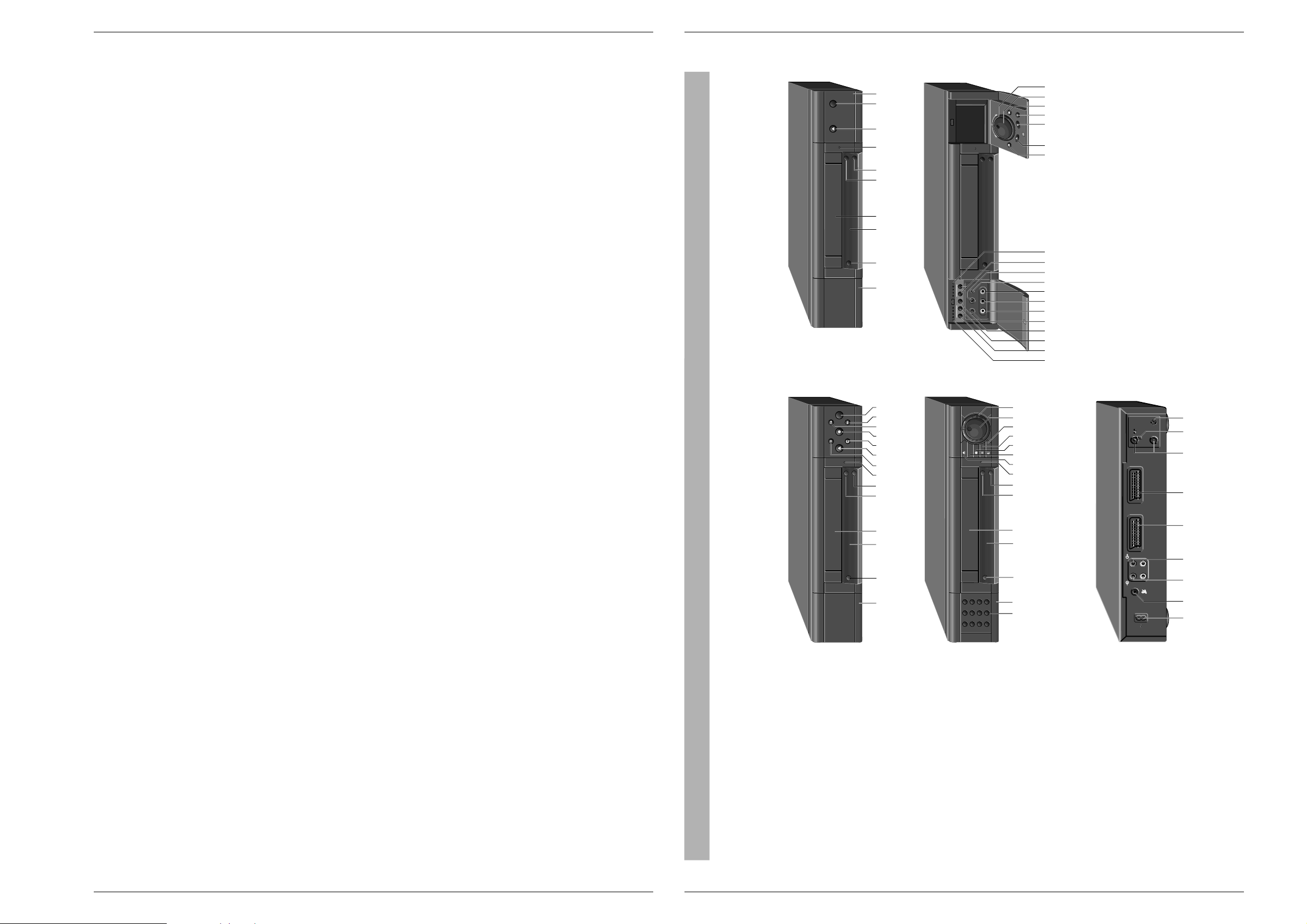
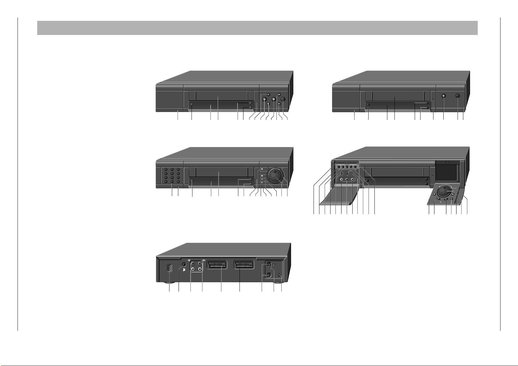
Bedienelemente
Hinweis:
Dieses Kapitel enthält Auszüge aus der Bedienungsanleitung.
Weitergehende Informationen entnehmen Sie bitte der
gerätespezifischen Bedienungsanleitung, deren Sachnummer Sie
in der entsprechenden Ersatzteilliste finden.
1
Ziffern-Tasten für verschiedene Eingaben
2
Geräteklappe links
3
Unterbricht/aktiviert die Aufnahmebereitschaft des
Recorders4Display5Cassettenfach
6
Zur Programmplatzwahl (bei Stop)
7
Zur Programmplatzwahl (bei Stop)
8
Standby Leuchtdiode
9
Cassettenauswurf
0
Startet die Wiedergabe
!
Aufnahme-Taste
@
Pause bei Aufnahme
Standbild bei Wiedergabe
#
Schaltet den Recorder ab (standby)
$
Bildsuchlauf vorwärts (bei Wiedergabe)
Vorlauf (bei Stop)
%
Bildsuchlauf rückwärts (bei Wiedergabe)
Rücklauf (bei Stop)
^
Jogscheibe
&
Shuttlering*Geräteklappe rechts
(
Aussteuerung Anzeige (links)
)
Insert-Schnitt
¡
Umschaltung auf Kopfhörer
™
Umschaltung auf manuelle Aussteurung bei Aufnahme
£
Mikrofoneingang
≤
Audioeingang Links (Camcorder)
∞
Audioeingang Rechts (Camcorder)
§
Videoeingang (Camcorder)
≥
„Synchro Edit“-Buchse
•
Kopfhörerbuchse
ª
Für die Lautstärke des Kopfhörers;
für die manuelle Aussteuerung bei Aufnahme;
für die Programmplatzwahl bei Timer Aufnahme.
º
Aussteuerung Anzeige (rechts)
⁄
Netzanschluß
¤
Fernbedienbuchse für Sat-Anlagen
‹
Audioeingang
›
Audioausgang
fi
EURO-AV1-Buchse (In / Out)
fl
EURO-AV2-Buchse (Pay-TV)
‡
Antennenbuchsen
°
Dämpfungsschalter für Antennenbuchsen
·
Kanaleinsteller
%
TIMER
ON/OFF
%
e
%
TIMER
ON/OFF
%
e
e
%
TIMER
ON / OFF
%
1 234 567 8 9
SV
0
AV
12
-
630+3 3+036
-
12
dB dB
VIDEO INL AUDIO IN R
MANINS./DUB.
-
LEVEL +
SYNC.
EDIT
U
I
MIC.
%
TIMER
ON/OFF
%
dB
L
H
L
H
x
x
+
+
–
–
EURO-AV A1
AUDIO
R
L
R
L
DECODER A2
@
64
$%
12 5 7
9
@80 &
0!
£™º
9@#^&
⁄
¤‹
()¡
flfi›
3^!#
642579803!#
64257980*3
≥§≤∞ ª•
·‡°
Allgemeiner Teil / General GV 54…, GV 56…, SE 5106…
Meßgeräte / Meßmittel
Regeltrenntrafo Farbgenerator
Zweikanaloszilloskop Tongenerator
Digitalmultimeter Stabilisiertes Netzgerät
Millivoltmeter Frequenzzähler
Beachten Sie bitte das Grundig Meßtechnik-Programm, das Sie unter
folgender Adresse erhalten:
Grundig electronics GmbH
Würzburger Str. 150
D-90766 Fürth/Bay.
Tel. 0911/703-0
Telefax 0911/703-4479
Testcassette..................................................................9.27540-1011
Testcassette (HiFi) ........................................................9.27540-1016
Drehmomentmesser 600gf-cm..................................... 75987-262.72
Adapter .........................................................................75987-262.73
Einstellschraubendreher ...............................................75987-262.80
Bandzug-Einstellgriff und -stift ..................................... 75988-002.27
Kopfscheibenabzieher ..................................................75988-002.37
Nylonhandschuhe .........................................................handelsüblich
Tentelometer .................................................................handelsüblich
Adapterkabel (16-polig).................................................75988-010.78
Adapterkabel (7-polig)...................................................75988-031.20
Diese Meßmittel können Sie über die Serviceorganisation beziehen.
Wir weisen jedoch darauf hin, daß es sich hierbei z.T. um Meßmittel
handelt, die am Markt bereits eingeführt sind.
Testcassette Sach-Nr. 9.27540-1011
• Farbtestbild mit Dropout-Einblendung
• 6,3kHz-Senkrecht-Vollspuraufzeichnung und Bezugspegel 333Hz
in dreiminütigem Wechsel.
Testcassette (HiFi) Sach-Nr. 9.27540-1016
• Farbtestbild mit Dropout-Einblendung
• Längsspur-Ton: 6,3kHz und 333Hz
• FM-Ton: 1kHz Vollpegel (± 50kHz Hub)
Video-Lehrfilm Sach-Nr. 72007-744.81
• Laufwerk "High Speed Drive"
Sach-Nr.
Test Equipment / Aids
Variable isolating transformer Colour generator
Dual channel oscilloscope AF Generator
Digital multimeter Stabilized power supply
Millivoltmeter Frequency counter
Please note the Grundig Catalog "Test and Measuring Equipment"
obtainable from:
Grundig electronics GmbH
Würzburger Str. 150
D-90766 Fürth/Bay.
Tel. 0911/703-0
Telefax 0911/703-4479
Part no.
Test cassette.................................................................9.27540-1011
Test cassette (HiFi) .......................................................9.27540-1016
Torquemeter 600gf-cm..................................................75987-262.72
Adapter .........................................................................75987-262.73
Adjustment screw driver................................................75987-262.80
Tape tension adjustment tool - handle and - pin .......... 75988-002.27
Headwheel extractor .....................................................75988-002.37
Nylon gloves ....................................................... commonly available
Tentelometer ....................................................... commonly available
Adapter cabel (16 pin)...................................................75988-010.78
Adapter cabel (7 pin).....................................................75988-031.20
You can order these test equipments from the Service organization.
We refer to you that these test equipments are already obtainable on
the market.
Test cassette Part no. 9.27540-1011
• Colour test pattern with dropout recording
• 6.3kHz vertical full-track recording alternating with 333Hz reference
level every 3 minutes.
Test cassette (HiFi) Part no. 9.27540-1016
• Colour test pattern with dropout recording
• Longitudinal track sound: 6.3kHz and 333Hz
• FM sound: 1kHz full level (± 50kHz deviation)
Video Training Film Part no. 72007-744.81
• Drive mechanism "High Speed Drive"
Technische Daten
VHS-System
1/2” Video - Cassettenrecorder
Bandgeschwindigkeit ................................2,339cm/s (Standard play)
Aufzeichnungsgeschwindigkeit .................... 4,84m/s (Standard play)
Umspulzeit bei Vor-/Rücklauf mit E180-Cassette: ............ typisch 95s
FS-Norm
CCIR, B/G/H - PAL
CCIR, I - PAL
CCIR, B/G - SECAM
Video
Signal / Rauschabstand
Standard play: ......................................................... ≥48dB (bewertet)
Longplay: ................................................................ ≥45dB (bewertet)
Auflösung ............................................................................. ≥3,1MHz
Ton
Frequenzgang
Standard play: ..................................................... 80Hz…10kHz ≤8dB
Longplay: .............................................................. 80Hz…5kHz ≤8dB
HiFi-Betrieb: ..................................................................20Hz…20kHz
Störabstand:
Standardton: ........................................................... ≥43dB (bewertet)
HiFi-Ton: ................................................................. ≥80dB (bewertet)
Gleichlaufschwankung: ........................................ ≤0,3% (DIN 45507)
Netzspannung .......................................................... 220V~…240V~
Netzfrequenz......................................................................47…63Hz
Leistungsaufnahme
– Aufnahme............................................................................ca. 18W
– EE-Betrieb...........................................................................ca. 16W
– Standby (Energiesparbetrieb, Modulator aus) ......................... <6W
Umgebungstemperatur............................................. +10°C…+35°C
Relative Luftfeuchte................................................................≤ 80%
Betriebslage ...................................................................... horizontal
1 - 5 GRUNDIG Service
Specification
VHS-System
1/2” video cassette recorder
Tape speed ...............................................2.339cm/s (Standard play)
Head to tape speed...................................... 4.84m/s (Standard play)
Winding time of forward wind/rewind of a E180 Cassette:.......typically 95s
TV standard
CCIR, B/G/H - PAL
CCIR, I - PAL
CCIR, B/G - SECAM
Video
Signal / noise ratio
Standard play: .........................................................≥48dB (weighted)
Longplay: ................................................................≥45dB (weighted)
Video resolution ................................................................... ≥3.1MHz
Sound
Frequency response
Standard play: ..................................................... 80Hz…10kHz ≤8dB
Longplay: .............................................................. 80Hz…5kHz ≤8dB
HiFi mode:.....................................................................20Hz…20kHz
Signal / noise ratio:
Standard Sound: .....................................................≥43dB (weighted)
HiFi Sound: .............................................................≥80dB (weighted)
Wow and flutter: ................................................... ≤0.3% (DIN 45507)
Mains voltage ........................................................... 220V~…240V~
Mains frequency................................................................ 47…63Hz
Power consumption
– Record ........................................................................ approx. 18W
– EE mode ..................................................................... approx. 16W
– Standby mode (min. power consumption, Modulator off) .......... <6W
Ambient temperature .............................................. +10°C … +35°C
Relative humidity ....................................................................≤ 80%
Operating position ............................................................ horizontal
1 - 6 GRUNDIG Service
Page 5

GV 54…, GV 56…, SE 5106… Allgemeiner Teil / General
GRUNDIG Service 1 - 7
4
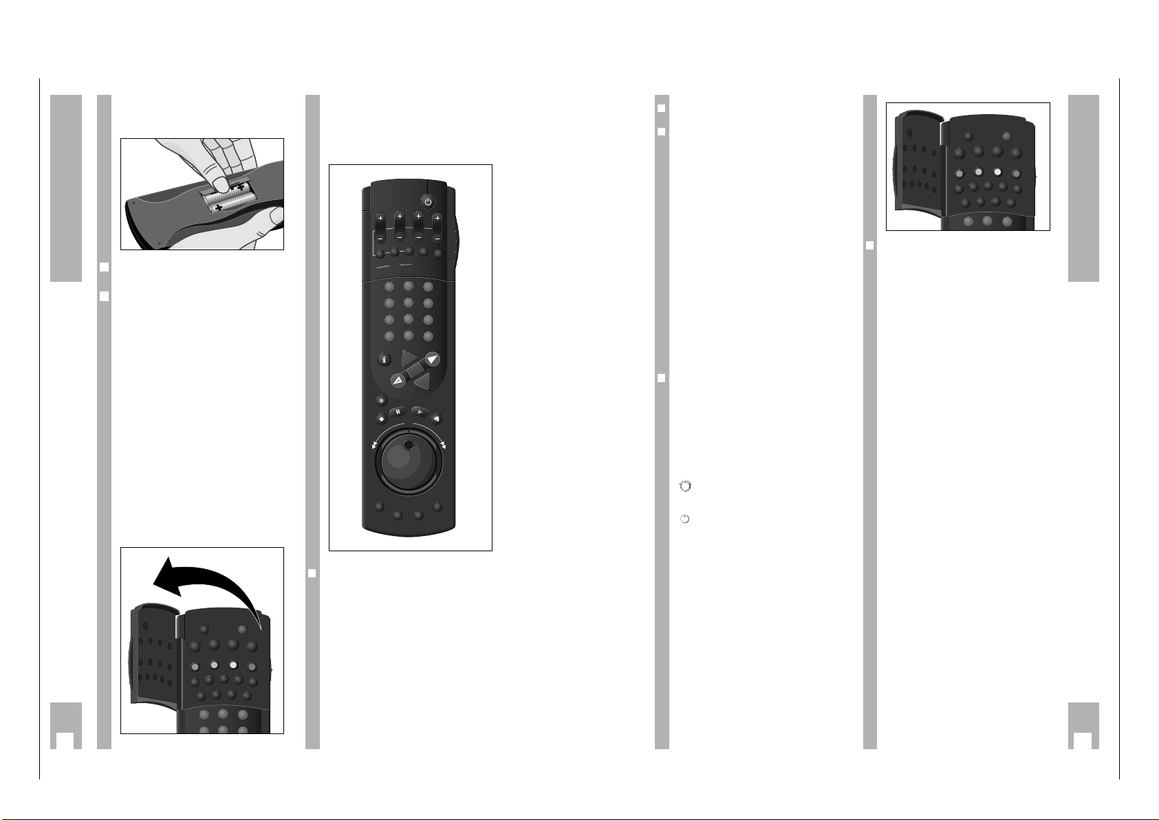
Die Fernbedienung
Batterien in die Fernbedienung
einlegen
Batteriefachdeckel abnehmen, dazu Schnapper
drücken und Deckel abnehmen.
Batterien (2x1,5 V, Typ Micro R03P) einsetzen.
w
!
Polung der Batterien beachten; im Batteriefachboden markiert.
w
!
Wenn Ihr Recorder auf die Fernbedienbefehle nicht
mehr richtig reagiert, können die Batterien verbraucht sein.
Verbrauchte Batterien unbedingt entfernen.
Für Schäden, die durch ausgelaufene Batterien entstehen, kann nicht gehaftet werden.
Verbrauchte Batterien gehören in den Sondermüll
(Umweltschutz).
Die zwei Ebenen der
Fernbedienung
Die Tasten der Fernbedienung sind auf zwei Ebenen
angeordnet.
Auf der oberen Ebene finden Sie die Tasten, die Sie
für wesentliche Bedienfunktionen benötigen.
Auf der Ebene unter der Klappe finden Sie die
Tasten für Komfortfunktionen.
3
5
2
1
´8
#
<
f
STOP
TIP
INS/DUB
PAL/SEC
CODE
RESET
AUDIO
COUNTER
SAT
ED/EW
VPS
C/S
2
1
Auf einem Blick
Auf dieser und der nächsten Seite sind die Tasten
der Fernbedienung kurz erklärt. Die Bedienung entnehmen Sie bitte dem jeweiligen Kapitel dieser
Bedienungsanleitung.
❒
Tasten für die TIMER-Programmierung
A Schaltet den Recorder ab (stand-by).
B PROG. Wählt das Programm.
B DAY Wählt den Tag.
B START Wählt die Startzeit.
B STOP Wählt die Stoppzeit.
¢
SET/CHECK Wählt die Tafel »Aufnahmeprogram-
mierung« an, zur Kontrolle und zum
Ändern von Daten.
¢
CLEAR Löscht Daten.
¢
ON/OFF Unterbricht/aktiviert die TIMER-
Aufnahme.
➡
❒
Schalter zur Wahl der Videoebene
❒
Tasten für verschiedene Eingaben
¢
SP/LP Schaltet auf Langspiel-Betrieb und
wieder zurück auf StandardspielBetrieb.
¢
SV/V+ Eröffnet die ShowView Programmie-
rung.
1
...
0
Ziffern-Tasten für verschiedene Eingaben.
g
Blendet bei der TIMER-Programmierung die in der Sender-Tabelle
gespeicherte Videotext-Seite am
Bildschirm ein.
e
Wählt Programmplatz A1, A 2 oder
CV für die Aufnahme bzw. für die
TIMER-Programmierung.
h
Schaltet auf die Info-Tafel und
zurück auf das Fernsehbild.
C Cursor-Tasten,
FE zum Bewegen des Cursors
D (Schreibmarke);
zum Anwählen verschiedener
Funktionen;
zum Feinabstimmen der Programme.
G
Bestätigt Daten.
❒
Lauffunktions-Tasten und Jog/Shuttle
K Startet die Aufnahme.
H Beendet alle Funktionen (Stopp).
W Pause bei Aufnahme,
Standbild bei Wiedergabe.
T Startet die Wiedergabe.
N Schiebt die Cassette aus.
Shuttle-Ring, zum Anwählen verschiedener Wiedergabegeschwindigkeiten bei Wiedergabe;
zum vor-/rückspulen bei Stopp.
Jog-Drehscheibe, schaltet das
Standbild weiter;
verändert die Zeitlupengeschwindigkeit.
¢
INDEX Wählt die INDEX-Such-Funktion.
¢
INDEX MARK Setzt Marken.
¢
INDEX ERASE Löscht Marken.
¢
TRACKING Aktiviert die Tracking-Funktion.
5
Die Fernbedienung
❒
Tasten unter der Klappe
¢
´
Ruft die Uhrzeit auf.
¢
8
Schaltet den Recorder ab (stand-by).
¢
#
Wählt Seite 100 (Übersicht) im
Videotext-Betrieb.
¢
Gibt verdeckte Informationen im
Videotext-Betrieb frei.
¢
<
Vergrößert die Zeichenhöhe im
Videotext-Betrieb.
¢
s
Hält Mehrfachseiten im VideotextBetrieb an.
Z VPS (rot) Schaltet die VPS/PDC-Steuerung
aus/ein; blättert im Videotext-Betrieb
um eine Seite zurück.
Z ED/EW (grün) Wählt eine ”wöchentliche” oder ”täg-
liche” Aufzeichnung (bei der TIMERProgrammierung); blättert im Videotext-Betrieb um eine Seite vor.
Z (gelb) Zum Wählen von Kapiteln im Video-
text-Betrieb.
Z C/S(blau) Schaltet von Kanalzahl auf Sonder-
kanalzahl;
zum Wählen von Themen im Videotext-Betrieb.
¢
Taste ohne Funktion.
¢
PAL/SEC Schaltet die Farbnorm (PAL oder
SECAM) um.
¢
INS/DUB Zum Anwählen von Insert- und Dub-
bing-Funktionen.
¢
TIP Zum Ein-/Ausblenden einer Titelzeile
in die Aufnahme.
¢
CODE Zur Vorwahl verschiedener Sonder-
funktionen.
¢
COUNTER Schaltet zwischen Spielzeit- und
Bandlängenanzeige um.
¢
RESET Schaltet die Bandlängenanzeige auf
00000.
¢
AUDIO Zur Tonspurwahl bei Aufnahme und
Wiedergabe;
zum Ein- und Ausschalten des
Tones bei Betrieb mit Bildschirmdialog.
¢
SAT Taste ohne Funktion.
3
2
1
´8
#
<
f
STOP
TIP
INS/DUB
PAL/SEC
CODE
RESET
AUDIO
COUNTER
SAT
ED/EW
VPS
C/S
DAY START
ON/OFF
STOP
SP/LP
SV/V+
2
3
5
6
8
9
0
AVVPT
+
+
OK
PROG.
SET/CHECK
CLEAR
TIMER
1
4
7
-
I
N
D
E
X
IN
D
E
X
M
A
R
C
A
R
T
E
S
A
R
E
X
E
K
D
I
N
G
N
I
K
Page 6

Allgemeiner Teil / General GV 54…, GV 56…, SE 5106…
1 - 8 GRUNDIG Service
6
Die Benutzerführung
GRUNDIG Benutzerführung am Bildschirm des Fernsehgerätes
… bietet den Dialog zwischen Ihnen und dem
Recorder.
Viele Funktionen, die Sie mit der Fernbedienung
anwählen, beantwortet der Recorder mit Info-Tafeln
und Dialogzeilen am Bildschirm des Fernsehgerätes.
Tastensymbole der Fernbedienung und Dialogzeilen
zeigen die nächsten und möglichen Bedienschritte.
Sie werden Schritt für Schritt, einfach und verständlich geführt.
❒
Vorbereiten
Fernsehgerät einschalten.
Am Fernsehgerät den Programmplatz für den
Videorecorder wählen (AV-Programmplatz).
w
!
Ist der Recorder an ein Fernsehgerät mit Megalogic-Funktion angeschlossen, schaltet sich das Fernsehgerät nach Drücken der Taste h ein und schaltet automatisch auf den AV-Programmplatz.
w
!
Mit Taste
¢
<
kann die Info-Tafel vergrößert wer-
2
1
❒
Info-Tafel aufrufen
Taste h der Fernbedienung drücken.
1
GRUNDIG
TEXT-PROGRAMMING
Info
1 : Aufnahme-Programmierung
2 : A1/A2 Aufnahme-Bereitschaft
3 : Videotext
4 : Sonderfunktionen
5 : Installation
■ 10 CNN 01. 15:00 16:30
■
■
■
■
■
+/– : Timerdaten eingeben
: VPS/PDC Ein/Aus
: ED/EW Normal
LP/CL :Long Play/Timer löschen
CHECK :nächsten Timer
i :Zurück zum INFO Menü
Timer Prog. Datum Start Stop
Taste der Darstellung in der Funktion
Fernbedienung Info-Tafel und den
Dialogzeilen
❒
h i
Ruft die Info-Tafel auf und schaltet zurück zum Fernsehbild.
❒
1 2 … 90 0-9
Zum Anwählen der verschiedenen Funktionen aus der Info-Tafel;
zur direkten Eingabe von Daten.
❒
DC
%% &&
Zum schrittweisen Anwählen von Funktionen oder von Zeilen in einer Tafel.
❒
FE " !
Zum Umblättern von Tafeln, zum Anwählen von Daten und zum Ändern von
Einstellungen.
❒
B
+/
–
Zum schrittweisen Eingeben von Daten bei der TIMER-Aufnahme.
❒
Z VPS (rot)
Schaltet die VPS/PDC-Steuerung einer TIMER-Aufnahme aus und wieder ein.
❒
Z ED/EW (grün) Wählt eine ”tägliche”oder ”wöchentliche” Aufnahme bei der TIMER-
Programmierung.
❒ ¢
SP/LP
¢
CLEAR LP/CL
SL/LP: Schaltet auf Langspiel-Betrieb und wieder zurück auf Standardspiel-
Betrieb.
CL: Löscht TIMER-Daten.
7
Einstellungen
Fernsehgerät auf den Recorder
abstimmen
Das Fernsehgerät empfängt auf bestimmten
Kanälen die Programme verschiedener Sender.
Auch der Recorder sendet auf einem solchen Kanal
(UHF-Bereich, zwischen Kanal 30 und 40 ± 2
Kanäle), auf den Sie jetzt das Fernsehgerät
einstellen müssen.
Damit Sie diesen Kanal finden, ist im Recorder ein
”Sender” eingebaut, der ein Testbild sendet.
w
!
Diese Einstellung ist nicht notwendig, wenn der
Recorder und das Fernsehgerät mit einem EUROAV-Kabel verbunden sind (siehe Kapitel
”Anschließen“ auf Seite 3).
Um Bildstörungen zu vermeiden, schalten Sie in
diesem Fall den Sender des Recorders ab, siehe
Kapitel auf Seite 8.
❒
Vorbereiten
Fernsehgerät einschalten.
Am Fernsehgerät den Programmplatz für den
Videorecorder wählen (AV-Programmplatz).
❒
Abstimmen
Recorder mit Taste C einschalten.
Antennenkabel aus der Buchse
–II–
des Recorders
ziehen.
w
!
Im Recorder darf sich keine Cassette befinden.
– Der Recorder ”sendet” nach kurzer Zeit das Test-
bild.
– Anzeige am Recorder: »
TEST
«.
Am Fernsehgerät – im UHF-Bereich, zwischen Kanal
30 und 40 ± 2 Kanäle – das Testbild des Recorders
suchen und speichern.
– Wie das geht, steht in der Bedienungsanleitung
des Fernsehgerätes.
Antennenkabel in die Antennenbuchse
–II–
des
Recorders stecken.
Ist die Bildqualität in Ordnung, Einstellung mit
Taste A beenden.
w
!
Ist die Bildqualität nicht in Ordnung, gehen Sie nach
dem Kapitel ”Bildqualität verbessern”, auf der nächsten Seite.
w
!
Wenn der Recorder an ein Fernsehgerät mit 100HzTechnik angeschlossen ist, und wenn das Testbild
”springt” oder ”zittert”, dann muß der Recorder
angepaßt werden.
Nacheinander an der Fernbedienung die Taste
¢
CODE, die Ziffern-Tasten 8547 und die
Taste G drücken.
– Kurzzeitige Anzeige am Recorder: »ON«.
Wird der Recorder nach dieser Anpassung an ein
Fernsehgerät mit herkömmlicher 50Hz-Technik
angeschlossen, nacheinander die Taste
¢
CODE, die
Ziffern-Tasten 8546 und die Taste G
drücken.
– Kurzzeitige Anzeige am Recorder: »
OFF
«.
5
4
3
GRUNDIG CTI TESTBILD
Kein Empfang auf Programm 01
GRUNDIG
TESTBILD
2
1
2
1
➡
DAY START
PROG.
ON/OFF
CLEAR
SET/CHECK
TIMER
2
1
5
4
8
7
0
+
I
N
D
E
X
IN
D
E
X
M
A
R
K
e
TIMER
ON/OFF
STOP
SP/LP
SV/V+
3
6
9
AVVPT
+
OK
-
G
N
I
K
C
A
R
T
E
S
A
R
E
X
E
D
I
N
%
%
GRUNDIG
TEXT-PROGRAMMING
Dialogzeilen
Page 7
GV 54…, GV 56…, SE 5106… Allgemeiner Teil / General
GRUNDIG Service 1 - 9
8
Einstellungen
❒
Bildqualität verbessern
Wenn sich auf dem Bildschirm des Fernsehgerätes
Schlangenlinien zeigen, ist der eingestellte Kanal
mit einem Fernseh-Programm belegt.
In diesem Fall gehen Sie wie folgt vor:
Taste C drücken.
Am Fernsehgerät – im UHF-Bereich, zwischen
Kanal 30 und 40 ± 2 Kanäle – einen Kanal suchen,
der nicht mit einem Fernsehprogramm belegt ist
(nur Rauschen am Bildschirm).
Kanal am Fernsehgerät speichern (siehe Bedienungsanleitung des Fernsehgerätes).
Antennenkabel aus der Buchse
–II–
des Recorders
ziehen.
w
!
Im Recorder darf sich keine Cassette befinden.
– Der Recorder ”sendet” nach kurzer Zeit das Test-
bild.
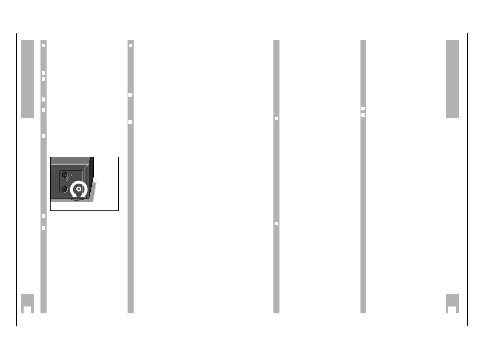
Kanaleinsteller q in der Rückseite des Recorders
(siehe Abbildung) mit einem passenden Schraubendreher etwas nach links oder rechts drehen, bis das
Testbild am Bildschirm des Fernsehgerätes
erscheint.
Antennenkabel wieder in die Buchse
–II–
des Recor-
ders stecken.
Einstellungen mit Taste A beenden.
7
6
L
H
L
H
x
x
+
+
–
–
5
4
3
2
1
❒
Sender des Recorders abschalten und
einschalten
Wenn viele Fernsehsender angeboten werden, die
Ihr Recorder im UHF-Bereich zwischen Kanal 30
und 40 empfängt, kann es zu Bildstörungen im
Recorder-Betrieb kommen. Deshalb kann der
Sender des Recorders abgeschaltet werden.
w
!
Damit das Bild-/Tonsignal des Recorders zu dem
Fernsehgerät gelangt, müssen die Geräte mit einem
EURO-AV-Kabel verbunden sein (siehe Seite 3).
Sender des Recorders abschalten, dazu nacheinander die Taste
¢
CODE, die Ziffern-Tasten
8518und die Taste G drücken.
– Der Sender des Recorders ist abgeschaltet.
– Kurzzeitige Anzeige am Recorder: »
OFF
«.
Sender des Recorders einschalten, dazu nacheinander die Taste
¢
CODE, die Ziffern-Tasten
8519und die Taste G drücken.
– Der Sender des Recorders ist eingeschaltet.
– Kurzzeitige Anzeige am Recorder: »ON«.
2
1
Fernseh-Programme einstellen
Die Fernsehanstalten senden ihre Programme
durch Fernsehsender auf verschiedenen Frequenzen/Kanälen.
Der Recorder hat dafür ein eigenes Empfangsteil.
Damit kann er – unabhängig vom Fernsehgerät –
die Fernseh-Programme empfangen und aufzeichnen.
Vorher müssen Sie die Kanäle der FernsehProgramme am Recorder einstellen.
Es stehen 99 Programmplätze zur Verfügung, die
beliebig mit Fernseh-Programmen von der Antenne,
Kabelanschluß oder vom Satelliten belegt werden
können.
❒
Die Möglichkeiten zum Einstellen der
Fernseh-Programme:
1. Durch die Übernahme der Daten vom Fernsehgerät.
Das Fernsehgerät muß mit Megalogic-Funktionen
ausgestattet sein.
2. Mit dem Suchlauf-Speicher-System (ATS euro
plus). Der Recorder sucht, sortiert und speichert
alle Kanalzahlen/Sonderkanalzahlen, die er an
seinem Standort empfangen kann.
Dieser Vorgang ist abhängig von der von Ihnen
gewählten Sprache, dem gewählten Land und der
Empfangsqualität der Fernseh-Programme.
Sollte Ihnen die vorgegebene Reihenfolge der
Fernseh-Programme nicht zusagen, können Sie
dies nachträglich ändern.
3. Durch direkte Eingabe der Daten.
4. Mit dem manuellen Suchlauf, wenn neue Fernseh-Programme hinzukommen, oder wenn der
Recorder ein Fernseh-Programm mit dem Suchlauf-Speicher-System nicht finden konnte.
❒
Hinweis zur TIMER-Programmierung
mit den Videotext-Seiten der
Sendeanstalten.
Bei dieser TIMER-Programmierung entnehmen Sie
die Daten für die Sendung (zum Beispiel Programm, Datum, Ein- und Ausschaltzeit) nicht mehr
aus den Programmzeitungen, sondern aus Programmübersichten, die Ihnen bestimmte Sendeanstalten auf Videotext-Seiten anbieten.
Die Nummern dieser Videotext-Seiten, auf denen
sich die Programmübersichten befinden, können
von Sendeanstalt zu Sendeanstalt verschieden sein.
Sie können jetzt entscheiden, aus welcher Seite der
Programmübersicht Sie die meisten Aufnahmen
programmieren wollen.
Geben Sie die benötigte Nummer der VideotextSeite in die »Sender-Tabelle« ein.
Wie das funktioniert, steht in dem Beispiel auf den
folgenden Seiten.
Bei der TIMER-Programmierung wird diese Videotext-Seite dann automatisch abgerufen.
Übernahme der Fernseh-Programme
vom Fernsehgerät
(Megalogic-Funktion)
Wird der Recorder an ein Fernsehgerät mit Megalogic-Funktion angeschlossen, übernimmt der
Recorder automatisch die im Fernsehgerät gespeicherten Fernseh-Programme.
Voraussetzung dafür ist, daß die folgende Bedienreihenfolge eingehalten wird.
w
!
Recorder und Fernsehgerät müssen mit dem beigepackten Megalogic-EURO-AV-Kabel verbunden
sein, das Fernsehgerät muß eingeschaltet sein.
Netzstecker des Recorders ziehen.
Netzstecker des Recorders wieder einstecken.
– Der Recorder übernimmt automatisch die Fern-
seh-Programme vom Fernsehgerät.
Dadurch erhält der Recorder die gleiche Belegung
mit Fernseh-Programmen wie das Fernsehgerät.
2
1
9
Einstellungen
➡➡
Page 8
Allgemeiner Teil / General GV 54…, GV 56…, SE 5106…
1 - 10 GRUNDIG Service
Fernseh-Programme einstellen,
mit dem Suchlauf-Speicher-System
(ATS euro plus)
❒
Vorbereiten
Fernsehgerät einschalten.
Am Fernsehgerät den Programmplatz für den
Videorecorder wählen (AV-Programmplatz).
❒
Beispiel
Suchlauf-Funktion anwählen, dazu nacheinander
die Taste h und die Ziffern-Tasten 5 und 1
drücken.
– Die Tafel »Sprachwahl« erscheint.
Sprache des Aufstellungsortes mit den Tasten
F E DC wählen und mit Taste G bestätigen.
Land (Aufstellungsort) mit den Tasten FE DC
wählen und mit Taste G bestätigen.
w
!
Ist in der Tafel das von Ihnen benötigte Land nicht
vorhanden, wählen Sie die Zeile »??«.
Suchlauf mit Taste G starten.
– Anzeige am Recorder: »
ATS
« und »A«.
– Der Recorder sucht alle Kanalzahlen nach Fern-
seh-Programmen ab, sortiert und speichert sie.
– Nach Abschluß des Suchlaufs erscheint die Tafel
»Sender-Tabelle«.
w
!
Bei Sendeanstalten, die ein VPS/PDC-Signal
senden, wird die Sender-Kurzbezeichnung automatisch in die »Sender-Tabelle« übernommen.
4
3
2
1
2
1
10
Einstellungen
Deutsch Portuguêse
Español Svenska
Français Norsk
English Dansk
Italiano Suomi
Nederlands
<
&
%
>:Wählen
OK :Bestätigen
i : Zurück zum INFO Menü
Sprachwahl
Prog. Kanal Sender VPT
k
11 06 ARD 304 150
12 34 ZDF 304 150
13 59 BR 3 304 150
14 40 RTL 303 150
15 36 SAT 1 303 150
16 21 PRO 7 100 150
17 53 ----- 100 150
18 56 ----- 100 150
19 24 ----- 100 150
10 - -
<
&
%
>:Programm wählen
■
: Sender sortieren/kopieren
OK :Eingabe ändern
CLEAR :Sender löschen
i : Zurück zum INFO Menü
Sender-Tabelle
w
!
Bei Sendeanstalten, die kein VPS/PDC-Signal
senden, erscheint in der »Sender-Tabelle«:
»Sender -----«, »VPT 100« und »k 150«, der
Programmplatz ist blau markiert.
Im Beispiel auf Seite 12 lesen Sie, wie Sie diese
Daten eingeben.
w
!
Wie Sie die Reihenfolge der Fernseh-Programme
ändern, Daten von Hand eingeben oder Daten
löschen, lesen Sie in den Beispielen auf den nächsten Seiten.
Einstellung mit Taste
¢
8
beenden.
❒
Bildstörungen beseitigen
Sollte der Recorder den ATS euro plus-Suchlauf
nicht ordnungsgemäß ausführen, Dämpfungsschalter in Stellung schieben und die Einstellung ab
Pkt. des Beispiels wiederholen.
L
H
L
H
x
x
+
+
–
–
L
H
L
H
1
H
5
➡
Fernseh-Programme umsortieren –
von Hand
❒
Vorbereiten
Fernsehgerät einschalten.
Am Fernsehgerät den Programmplatz für den
Videorecorder wählen (AV-Programmplatz).
❒
Beispiel
»Sender-Tabelle« anwählen, dazu nacheinander die
Taste h und die Ziffern-Tasten 5 und 3 drücken.
– Die »Sender-Tabelle« erscheint, der gewählte
Programmplatz ist markiert.
Programmplatz mit den Tasten DC E F
anwählen.
Programmplatz mit Taste Z ED/EW (grün) markieren.
Neuen Programmplatz mit den Tasten DC
anwählen.
– Die Daten des markierten Programmplatzes wer-
den an den neuen Programmplatz verschoben.
Einstellungen mit Taste G speichern.
– Die folgenden Fernseh-Programme verschieben
sich um eine Position.
Zum Umsortieren von weiteren Fernseh-Programmen Vorgang ab Pkt. wiederholen.
Einstellung mit Taste
¢
8
beenden.
6
2
5
4
3
2
1
2
1
Fernseh-Programme umsortieren –
mit der Follow TV-Funktion
Hierbei erhält der Recorder die gleiche Programmplatzbelegung wie das Fernsehgerät.
w
!
Recorder und Fernsehgerät müssen mit einem
EURO-AV-Kabel verbunden sein.
❒
Vorbereiten
Fernsehgerät einschalten.
Am Fernsehgerät den Programmplatz für den
Videorecorder wählen (AV-Programmplatz).
❒
Beispiel
Funktion Follow-TV anwählen, dazu nacheinander
die Taste h und die Ziffern-Tasten 5 und 2
drücken.
– Anzeige am Recorder: »
SELECT TV POI
«.
Am Fernsehgerät den Programmplatz 1 wählen.
An der Fernbedienung des Recorders Taste G
drücken.
– Anzeige am Recorder: »
PLEASE WAIT
«.
– Der Recorder ”sucht” nach den Daten des ersten
Programmplatzes des Fernsehgerätes. Er belegt
seinen ersten Programmplatz mit dem gleichen
Fernseh-Programm wie am Fernsehgerät.
– Ist dieser Vorgang beendet, erscheint in der
Anzeige des Recorders: »
SELECT TV PO2
«.
Am Fernsehgerät Programmplatz 2 wählen.
An der Fernbedienung des Recorders Taste G
drücken.
– Einstellung so oft wiederholen, bis alle Fernseh-
Programme sortiert sind.
Einstellung mit Taste
¢
8
beenden.
w
!
Wenn bei dieser Einstellung zwei Fernsehanstalten
das gleiche Programm senden, kann es zu Fehlern
in der Zuordnung führen.
Einstellung bei unterschiedlichen Programminhalten wiederholen.
6
5
4
3
2
1
2
1
11
Einstellungen
Prog. Kanal Sender VPT
k
11 06 ARD 304 150
12 34 ZDF 304 150
13 59 BR 3 304 150
14 40 RTL 303 150
15 36 SAT 1 303 150
16 21 PRO 7 100 150
17 53 NTV 100 150
18 56 ----- 100 150
19 24 ----- 100 150
10 - -
<
&
%
>:Programm wählen
■
: Sender sortieren/kopieren
OK :Eingabe ändern
CLEAR :Sender löschen
i : Zurück zum INFO Menü
Sender-Tabelle
➡
Prog. Kanal Sender VPT
k
11 06 ARD 304 150
12 34 ZDF 304 150
13 59 BR 3 304 150
14 40 RTL 303 150
15 36 SAT 1 303 150
16 21 PRO 7 100 150
17 53 ----- 100 150
18 56 ----- 100 150
19 24 ----- 100 150
10 - -
<
&
%
>:Programm wählen
■
: Sender sortieren
OK :Eingabe ändern
CLEAR :Sender löschen
i : Zurück zum INFO Menü
Sender-Tabelle
Prog. Kanal Sender VPT
k
11 06 ARD 304 150
12 34 ZDF 304 150
13 59 BR 3 304 150
14 21 PRO7 100 150
15 36 SAT 1 303 150
16 40 RTL 303 150
17 53 NTV 100 150
18 56 ----- 100 150
19 24 ----- 100 150
10 - -
<
&
%
>:Programm wählen
■
: Sender sortieren/kopieren
OK :Eingabe ändern
CLEAR :Sender löschen
i : Zurück zum INFO Menü
Sender-Tabelle
GRUNDIG
ATS euro plus
GRUNDIG
ATS euro plus
GRUNDIG
TEXT-PROGRAMMING
GRUNDIG
TEXT-PROGRAMMING
GRUNDIG
TEXT-PROGRAMMING
Page 9
GV 54…, GV 56…, SE 5106… Allgemeiner Teil / General
GRUNDIG Service 1 - 11
Daten von Hand eingeben
❒
Vorbereiten
Fernsehgerät einschalten.
Am Fernsehgerät den Programmplatz für den
Videorecorder wählen (AV-Programmplatz).
❒
Beispiel
»Sender-Tabelle« anwählen, dazu nacheinander die
Taste h und die Ziffern-Tasten 5 und 3 drücken.
– Die »Sender-Tabelle« erscheint, der gewählte
Programmplatz ist markiert.
Programmplatz mit den Tasten DC E F
anwählen, danach Taste G drücken.
– Die Tafel »Programm« erscheint.
Datenzeile mit den Tasten DC anwählen.
Die Texte bedeuten:
Sat – Satelliten-Fernseh-Programm
(die Einstellung »Sat: Ja« kann
nur gewählt werden, wenn ein
externer Satelliten-Empfänger
an Buchse EURO-AV DECODER
A2 angeschlossen ist).
Kanal – die Kanalzahl oder die Fre-
quenz des Fernseh-Programms,
Name – die Sender-Kurzbezeichnung
(max. 5 Stellen),
Norm – PAL oder SEC-Farbnorm,
Decoder – Programmplatz für externen
Decoder aktivieren,
Feinabstimmung – Bild feinabstimmen,
Text-Seite – die Nummer der Seite,
Untertitel-Seite – die Nummer der Seite.
w
!
Die weitere Bedienung entnehmen Sie bitte den Dialogzeilen der »Programm«-Tafel.
3
2
1
2
1
w
!
Für Satelliten-Fernseh-Programme geben Sie die
Sender-Kurzbezeichnung und die Nummer der
Videotextseite auf den gleichen Programmplätzen
ein, wie im Satelliten-Empfänger.
Weitere Einstellungen sind nicht möglich.
w
!
Alternativ zur Eingabe der Kanalzahl kann die Frequenz des Fernseh-Programms eingegeben werden
oder ein Suchlauf gestartet werden.
w
!
Nach dem Bestätigen der Untertitel-Seitennummer
erscheint wieder die »Sender-Tabelle«.
Zur Dateneingabe für die nächsten Programmplätze
Einstellung ab Pkt. wiederholen.
Einstellung mit Taste
¢
8
beenden.
Daten eines Programmplatzes
löschen
❒
Vorbereiten
Fernsehgerät einschalten.
Am Fernsehgerät den Programmplatz für den
Videorecorder wählen (AV-Programmplatz).
❒
Beispiel
»Sender-Tabelle« anwählen, dazu nacheinander die
Taste h und die Ziffern-Tasten 5 und 3 drücken.
– Die »Sender-Tabelle« erscheint, der gewählte
Programmplatz ist markiert.
Programmplatz mit den Tasten DC E F
anwählen.
Datenzeile mit Taste
¢
CLEAR löschen.
– Die folgenden Fernseh-Programme rücken um
einen Programmplatz vor.
Einstellung mit Taste
¢
8
beenden.
4
3
2
1
2
1
4
2
12
Einstellungen
Sat: Nein
Kanal: C
■
39
Name: -----
Norm: PAL
Decoder: OFF
Feinabstimmung: -3
Text-Seite: 301
Untertitel-Seite: 320
0-9/< > : Kanal eingeben/suchen
: Sonderkanal ein/aus
: Frequenz/Kanal-Eingabe
&
%
: Wählen
OK : Bestätigen
: TV-Bild
i : Zurück zum INFO Menü
Programm 12
Prog. Kanal Sender VPT
k
11 06 ARD 304 150
12 34 ZDF 304 150
13 59 BR 3 304 150
14 40 RTL 303 150
15 36 SAT 1 303 150
16 21 PRO 7 100 150
17 53 ----- 100 150
18 56 ----- 100 150
19 24 ----- 100 150
10 - -
<
&
%
>:Programm wählen
■
: Sender sortieren/kopieren
OK :Eingabe ändern
CLEAR :Sender löschen
i : Zurück zum INFO Menü
Sender-Tabelle
❒
Vorbereiten
Fernsehgerät einschalten.
Am Fernsehgerät den Programmplatz für den
Videorecorder wählen (AV-Programmplatz).
Bespielte Cassette in das Cassettenfach schieben.
Der Videorecorder stellt automatisch die Spielzeit
der Cassette fest.
❒
Bedienung
Wiedergabe mit Taste T starten.
Pause/Standbild anwählen, dazu während der Wie-
dergabe Taste W drücken.
Standbilder schrittweise weiterschalten, – vor-
wärts/rückwärts, dazu während Wiedergabe-Pause
die Jog-Drehscheibe nach rechts oder links drehen.
Verschiedene Wiedergabegeschwindigkeiten anwählen, – vorwärts/rückwärts, dazu während der
Wiedergabe den Shuttle-Ring nach rechts oder
links drehen.
Die Abbildung zeigt die Möglichkeiten.
2-fach
5-fach
7-fach
11-fach
5-fach
7-fach
11-fach
1/2
1/12
1/2
1/12
+
–
0
11
Z
e
i
t
l
u
p
e
N
o
r
m
a
l
S
c
h
n
e
l
l
S
u
c
h
l
a
u
f
S
t
a
n
d
b
il
d
Z
e
i
tl
u
p
e
N
o
r
m
a
l
S
c
h
n
e
l
l
S
u
c
h
l
a
u
f
W
i
e
d
e
r
g
a
b
e
v
o
r
w
ä
r
t
s
W
i
e
d
e
r
g
a
b
e
r
ü
c
k
w
ä
r
t
s
3-fach
4
3
2
1
3
2
1
w
!
Während der Zeitlupe kann mit der Jog-Drehscheibe die Zeitlupengeschwindigkeit verändert werden.
w
!
Aus den Wiedergabe-Funktionen Pause/Standbild
und den verschiedenen Wiedergabefunktionen
zurück zur normalen Wiedergabe, dazu Taste T
drücken.
Wiedergabe mit Taste H beenden.
Band vor-/zurückspulen, dazu in Funktion Stopp
Shuttle-Ring nach rechts oder links drehen.
Umspulen mit Taste H beenden.
Cassette entnehmen, dazu Taste N drücken.
Recorder mit Taste A der Fernbedienung abschalten.
❒
Megalogic-Funktion
Ist der Recorder an ein Fernsehgerät mit Megalogic-Funktionen angeschlossen, schaltet sich das
Fernsehgerät nach dem Starten der Wiedergabe ein
und schaltet automatisch auf den AV-Programmplatz.
8
7
6
5
14
Wiedergabe
%
%
➡
Auf einem Blick
17
8
1
7
2
5
4
3
6
2 3 4
6
5
GRUNDIG
TEXT-PROGRAMMING
GRUNDIG
TEXT-PROGRAMMING
GRUNDIG
TEXT-PROGRAMMING
DAY START
PROG.
SET/CHECK
TIMER
1
4
7
STOP
ON/OFF
SP/LP
CLEAR
SV/V+
2
3
5
6
8
9
0
AVVPT
+
+
OK
-
I
N
D
E
X
IN
D
E
X
M
R
T
E
S
A
R
E
A
X
R
E
K
D
I
N
G
N
I
K
C
A
Page 10
Allgemeiner Teil / General GV 54…, GV 56…, SE 5106…
1 - 12 GRUNDIG Service
Zusatzfunktionen der Wiedergabe
❒
Wiedergabe von Langspielaufzeichnungen
Bei der Wiedergabe einer Langspiel-Aufzeichnung
schaltet der Recorder automatisch auf LangspielWiedergabe.
– Anzeige am Recorder: »LP«
w
!
Bei Langspiel-Betrieb können Bildstörungen auftreten.
❒
Wiedergabe von Aufzeichnungen anderer
Farbnormen
SECAM-Farbnor
m
Bei der Wiedergabe von SECAM-Aufzeichnungen
Taste
¢
PAL/SEC drücken.
– Anzeige am Recorder: »
SEC
«.
w
!
Auch das Fernsehgerät muß dieser Farbnorm entsprechen.
Am Ende dieser Wiedergabe Taste
¢
PAL/SEC noch
einmal drücken, die Anzeige »
SEC
« erlischt.
NTSC-Farbnorm
Bei der Wiedergabe von NTSC-Aufzeichnungen
schaltet der Recorder automatisch auf dieses
System.
– Kurzzeitige Anzeige am Recorder:
»
NTSC SP
« (Standard Play) oder
»
NTSC EP
« (Extended Play).
w
!
Die Anzeige der Gesamtspielzeit wechselt auf fünfstellige Bandlängenanzeige.
w
!
Bei NTSC-Wiedergabe ist keine Standbild-Funktion
möglich.
w
!
Bei NTSC-Langspiel-Wiedergabe können Bildstörungen auftreten.
❒
Wiedergabe von S-VHS-Aufzeichnungen
Bei der Wiedergabe von Cassetten, die im S-VHS
Format aufgezeichnet wurden, schaltet der Recorder automatisch auf dieses System.
– Anzeige am Recorder » «.
❒
Tonspur wählen
Bei der Wiedergabe von Cassetten, die mit Stereooder Zweiton-Sendungen bespielt wurden, kann die
gewünschte Tonspur gewählt werden.
Grundstellung ist Stereo (HiFi-Schrägspur)
– Anzeige am Recorder: »)« und »
STEREO
«.
Aufeinanderfolgendes Drücken der Taste
¢
AUDIO
bewirkt:
Tonspur 1 – Anzeige am Recorder:
»I« und »
LEFT
«;
Tonspur 2 – Anzeige am Recorder: »2« und »
RIGHT
«.
Mono-/Längsspur – ohne Anzeige;
Mixbetrieb (HiFi-Schrägspur und Mono-/Längsspur, zur Kontrolle von nachvertonten Cassetten)
– Anzeige am Recorder: »
MIX
«.
Bild-/Tonkorrekturen
❒
Bild-/Tonkorrektur – automatisch
Nach dem Einschieben der Cassette und dem Starten der Wiedergabe stimmt der Recorder automatisch auf beste Bildqualität ab (Auto Tracking).
– Während der Abstimmung erscheint am Recorder
die Anzeige »
AUTO-TRACK
« und die Bild-/Ton-
qualität kann sich verändern.
❒
Bild-/Tonkorrektur – manuell
Taste
¢
TRACKING drücken.
– Anzeige am Recorder: »
TRACKING
«.
Tracking (Spurlage)-Einstellung mit den Tasten
F E
der Fernbedienung durchführen
Einstellung mit Taste Gspeichern.
❒
Bild-/Tonverbesserung für
fremdbespielte Cassetten
Wenn bei der Wiedergabe von fremdbespielten
Cassetten das Bild springt oder durchläuft, drücken
Sie nacheinander die Taste
¢
CODE, die Ziffern-
Tasten
8511
und Taste G.
– Kurzzeitige Anzeige am Recorder: »ON«.
❒
Bild-/Tonverbesserung für
fremdbespielte Cassetten
Wenn bei den Wiedergabefunktionen Standbild,
Zeitlupe vorwärts und Wiedergabe 2-fach vorwärts
das Bild zittert oder unruhig wirkt, kann es optimiert
werden.
Während der Wiedergabe nacheinander die Taste
h, die Ziffern-Taste 2 und Taste G drücken.
– Anzeige am Recorder: »
JITTER
«.
Mit den Tasten
D oder C
das Bild nach subjektiv
bestem Eindruck einstellen und dann Taste
G
drücken.
❒
Bildschärfe (Crispening) optimieren
Automatisch (Automatic Contour Control)
Nach dem Einschieben der Cassette und dem Starten der Wiedergabe stimmt der Recorder automatisch auf optimale Bildschärfe ab.
Manuell
Während der Wiedergabe kann mit den Tasten
DC
die Bildschärfe nach subjektiv bestem Bildeindruck eingestellt werden.
– Kurzzeitige Anzeige am Recorder:
»
SHARPNESS + I
«.
2
1
3
2
1
15
Wiedergabe
➡
❒
Vorbereiten
Fernsehgerät einschalten.
Am Fernsehgerät den Programmplatz für den
Videorecorder wählen (AV-Programmplatz).
Cassette mit ausreichender Spieldauer in das Cas-
settenfach schieben.
❒
Bedienung
Programmplatz wählen, schrittweise mit den Tasten
DC der Fernbedienung oder den Tasten c d
am Recorder;
direkt mit den Ziffern-Tasten 1 ... 0 der Fernbedienung.
w
!
Für zweistellige Programmplätze die Ziffern-Tasten
kurz hintereinander drücken.
Langspielaufnahme – wenn gewünscht – mit
Taste
¢
SP/LP der Fernbedienung wählen.
– Die Spieldauer der Cassette wird dadurch verdop-
pelt.
Aufnahme mit Taste K starten.
Aufnahmepause mit Taste W anwählen.
Aufnahme mit Taste K fortsetzen.
Aufnahme mit Taste H beenden.
Band vor-/zurückspulen, dazu in Funktion Stopp
Shuttle-Ring nach rechts oder links drehen.
Umspulen mit Taste H beenden.
Cassette entnehmen, dazu Taste N drücken.
Recorder mit Taste A der Fernbedienung abschal-
ten.
8
7
6
5
4
3
2
1
3
2
1
❒
Megalogic-Funktion
Ist der Recorder an ein Fernsehgerät mit Megalogic-Funktionen angeschlossen, kann mit Taste K
das Fernseh-Programm, das am Bildschirm des
Fernsehgerätes zu sehen ist, aufgezeichnet werden.
Der Programmplatz muß am Recorder nicht
gewählt werden.
17
Aufnahme
➡
Auf einem Blick
8
7
4
5
6
3
2
1
1
3
7
1
4 6
5
%
%
DAY START
ON/OFF
STOP
SP/LP
SV/V+
2
3
5
6
8
9
0
AVVPT
+
+
OK
PROG.
CLEAR
SET/CHECK
TIMER
1
4
7
-
I
N
D
E
X
IN
D
E
X
M
T
E
S
A
R
E
A
X
R
E
K
D
I
N
G
N
I
K
C
A
R
Page 11
GV 54…, GV 56…, SE 5106… Allgemeiner Teil / General
GRUNDIG Service 1 - 13
Sprache der Benutzerführung
wählen
Die Sprache der Benutzerführung kann geändert
werden.
Diese Änderung hat keinen Einfluß auf die Einstellung der Fernseh-Programme mit dem ATS euro
plus- Suchlauf.
❒
Vorbereiten
Fernsehgerät einschalten.
Am Fernsehgerät den Programmplatz für den
Videorecorder wählen (AV-Programmplatz).
❒
Bedienung
Nacheinander die Taste h und die Ziffern-Tasten
5 und 4 drücken.
– Die Tafel »Sprachwahl« erscheint.
– Die gewählte Sprache ist farbig markiert.
Gewünschte Sprache mit den Tasten DC F E
wählen und mit Taste G bestätigen.
– Der Recorder schaltet auf das Fernsehbild. Ab
jetzt erscheinen alle Info-Tafeln und Dialogzeilen
in der gewählten Sprache.
2
1
2
1
38
Sonderfunktionen
Uhrzeit und Datum
kontrollieren/einstellen
w
!
Die Digitaluhr läuft auch weiter, wenn der Recorder
vom Stromnetz getrennt ist (die Uhrzeit ist in der
Anzeige nicht sichtbar).
❒
Automatische Aktualisierung
Die Uhrzeit wird bei Videotext-Betrieb mit
Programmplatz 1 automatisch aktualisiert.
❒
Manuelle Einstellung
❒
Vorbereiten
Fernsehgerät einschalten.
Am Fernsehgerät den AV-Programmplatz für den
Videorecorder wählen (dient als Kontrollmonitor).
❒
Bedienung
Nacheinander die Taste h und die Ziffern-Tasten
5 und 5 drücken.
– Die Tafel »Uhrzeit/Datum stellen« erscheint.
Uhrzeit mit den Ziffern-Tasten 1 … 0 vierstellig
eingeben.
Mit Taste D die Zeile »Datum« anwählen und
Datum mit den Ziffern-Tasten 1 … 0 sechsstellig
eingeben.
Eingabe mit Taste G speichern.
Einstellung mit Taste h beenden.
5
4
3
2
1
2
1
Uhrzeit:❚8:00
Datum: 02.03.95
0-9 :Uhrzeit eingeben
%
: Datum wählen
OK :Uhrzeit und Datum speichern
i :Zurück zum INFO Menü
Uhrzeit/Datum stellen
Deutsch Portuguêse
Español Svenska
Français Norsk
English Dansk
Italiano Suomi
Nederlands
<
&
%
>:Wählen
OK :Bestätigen
i :Zurück zum INFO-Menü
Sprachwahl
39
Sonderfunktionen
Fernbedienen anderer GRUNDIGVideorecorder
Mit dieser Fernbedienung können verschiedene
GRUNDIG-Videorecorder unabhängig voneinander
bedient werden.
Ihren GV 560 und einen zweiten Videorecorder der
Serie VS 600 bis VS 900 und ab der Serie GV 200.
Damit die Recorder die Fernbedienungsbefehle
richtig auswerten können, muß der GV 560 umgestellt werden.
❒
Videoebene für den GV 560 einstellen
Nacheinander die Taste h und die Ziffern-Tasten
4 und 4 drücken.
– Die Tafel »Videoebene« erscheint.
Videoebene 2 mit den Tasten FEwählen.
Einstellung mit Taste G bestätigen.
– Der Recorder schaltet die Tafel ab.
❒
Fernbedienen der beiden Recorder
Schalter in Stellung VIDEO 2, Sie bedienen Ihren
GV 560;
Schalter in Stellung VIDEO 1; Sie bedienen den
zweiten Recorder.
w
!
Steht der Schalter VIDEO 1 2 bei der Bedienung des
GV 560 nicht in der gewählten Videoebene, signalisiert die Anzeige »
VID I
« bzw. »
VID 2
« am
Recorder, daß die Fernbedienung auf die andere
Videoebene umgeschaltet werden muß.
1
2
TV
1
2
TV
SP/LP
ON/OFF
CLEAR
SV/V+
STOP
TART
9
3
6
2
2
1
3
2
1
Fernsehgerät fernbedienen
Mit dieser Video-Fernbedienung können auch
GRUNDIG-Farbfernsehgeräte ab der Fernbedienung
TP 590 bedient werden.
w
!
Welche Funktion Sie tatsächlich bedienen können,
hängt von der Ausstattung des GRUNDIG-Fernsehgerätes ab.
❒
Vorbereiten
Fernsehgerät mit Netztaste einschalten.
Schalter der Fernbedienung in Stellung TV schieben.
w
!
Fernbedienung auf das Fernsehgerät richten.
❒
Bedienung
Mit den Tasten DC können die Programmplätze
schrittweise von 1 bis 99 weitergeschaltet werden.
Mit den Ziffern-Tasten 1 … 0 können die Programmplätze direkt angewählt werden.
Die Programmplätze A1, A2 usw. werden durch
wiederholtes Drücken der Taste e angewählt.
Lautstärke verändern
Taste F drücken, der Ton wird leiser.
Taste E drücken, der Ton wird lauter.
Bereitschaft/Stand-By
Bei Fernsehpausen kann das Fernsehgerät mit
Taste A in Bereitschaft geschaltet werden.
Mit Taste e wird das Fernsehgerät wieder eingeschaltet.
3
2
1
1
2
TV
1
2
TV
SP/LP
ON/OFF
CLEAR
SV/V+
STOP
ART
9
3
6
2
2
1
Videoebene 1
<>:Videoebene wählen
OK :Bestätigen
i :Zurück zum INFO-Menü
Videoebene
VIDEO 1
VIDEO 2
TV
VIDEO 1
VIDEO 2
TV
GRUNDIG
TEXT-PROGRAMMING
GRUNDIG
TEXT-PROGRAMMING
GRUNDIG
TEXT-PROGRAMMING
Page 12
Allgemeiner Teil / General GV 54…, GV 56…, SE 5106…
1 - 14 GRUNDIG Service
Operating Elements
Note:
This chapter contains excerpts from the operating instructions. For
further particulars please refer to the appropriate user instructions
part number of which is indicated in the relevant spare parts list.
1 Numbered buttons for various entries
2 Flap, left
3 Interrupts/activates the record stand-by mode of the
recorder
4 Display
5 Cassette compartment
6 For selecting programme positions (on stop)
7 For selecting programme positions (on stop)
8 Stand-by light emitting diode
9 Cassette eject
0 Starts playback
! Record button
@ Pause on Record
freeze-frame on playback
# Switches the recorder to stand-by
$ Forward picture search (on playback)
fast forward (on stop)
% Reverse picture search during playback
rewind (on stop)
^ Jog rotary disk
& Shuttle ring
* Flap, right
( Level control indicator (left)
) Insert-editing
¡ Switches over to headphone operation
™ Switches over to manual record level control
£ Microphone input
≤ Audio input left (camcorder)
∞ Audio input right (camcorder)
§ Video input (camcorder)
≥ Synchro Edit socket
• Headphone socket
ª for headphone volume level
for manual record level control
for programme position selection on timer
º Level control indicator (right)
⁄ Mains connection
¤ Remote control socket for SAT systems
‹ Audio input
› Audio output
fi EURO-AV1-socket (In / Out)
fl EURO-AV2-socket (Pay-TV)
‡ Aerial sockets
° Attenuation switch for aerial level
· Channel selection
TIMER
ON/OFF
1 2 3
4 5 6
7 8 9
SV0AV
12 5 7
⁄
TIMER
ON / OFF
3^!#
AUDIO
R
R
L
L
EURO-AV A1
¤‹
%
%
@
642579803!# 64257980*3
e
%
%
64
9
DECODER A2
flfi›
e
$%
@80 &
L
L
H
H
+
+
x
x
–
–
·‡°
()¡
dB
12 -630+3 3+036-12
dB dB
MANINS./DUB.
-
LEVEL +
U
SYNC.
MIC.
I
EDIT
VIDEO INL AUDIO IN R
ON/OFF
£™º
≥§≤∞ ª•
TIMER
ON/OFF
TIMER
%
%
%
%
0!
9@#^&
e
Page 13
GV 54…, GV 56…, SE 5106… Allgemeiner Teil / General
GRUNDIG Service 1 - 15
4
The Remote Control
Inserting batteries into the remote
control
Press the catch and remove the cover from the battery compartment.
Insert the batteries (2x1.5 V, type Micro R03P).
w
!
Observe correct polarity, as marked on the bottom
of the battery compartment.
w
!
If your recorder no longer responds correctly to the
remote control commands, the batteries may be
exhausted.
Exhausted batteries must be removed.
The manufacturer cannot be held responsible for
damage resulting from battery leakage.
Exhausted batteries must be properly disposed of
as special refuse (environmental protection).
The two levels of the
remote control
The buttons on the remote control are located on
two separate levels.
The buttons you need for essential operating functions are located on the upper level.
The buttons you need for convenience functions are
located on the level under the cover flap.
3
5
2
1
´8
#
<
f
STOP
TIP
INS/DUB
PAL/SEC
CODE
RESET
AUDIO
COUNTER
SAT
ED/EW
VPS
C/S
2
1
At a glance
The buttons on the remote control are explained
briefly on this page and the following page. Please
refer to the respective chapter of these operating
instructions for operation.
❒
Buttons for TIMER programming
A Switches the recorder off (stand-by).
B PROG. Selects the TV station.
B DAY Selects the day.
B START Selects the start time.
B STOP Selects the stop time.
¢
SET/CHECK Calls up the » Record Programming«
table, for checking and altering data.
¢
CLEAR Deletes data.
¢
ON/OFF Interrupts/activates TIMER recor-
ding.
➡
❒
Switch for selecting the VCR address
❒
Buttons for various entries
¢
SP/LP Switches to long-play mode and
back to standard-play mode.
¢
SV/V+ Opens ShowView programming.
1
...
0
Numbered buttons for various
entries.
g
During TIMER programming, displays the teletext page stored in the
TV station table.
e
Selects programme position A1, A 2
or CV for recording or for TIMER
programming.
h
Switches to the info table and back
to the television picture.
C Cursor buttons,
FE for moving the cursor
D (marker);
for selecting various functions;
for fine-tuning the programmes.
G
Confirms data.
❒
Drive mechanism buttons and Jog/
Shuttle
K Starts recording.
H Terminates all functions (Stop).
W Pause in recording mode,
freeze-frame in playback mode.
T Starts playback.
N Ejects the cassette.
Shuttle ring, for selecting various
playback speeds during playback;
for fast forward/rewind during stop.
Jog dial, advances the freeze-frame;
changes the slow motion speed.
¢
INDEX Selects the INDEX Search function.
¢
INDEX MARK Sets markers.
¢
INDEX ERASE Erases markers.
¢
TRACKING Activates the tracking function.
5
The Remote Control
❒
Buttons under the cover flap
¢
´
Calls up the time of day.
¢
8
Switches the recorder off (stand-by).
¢
#
Selects page 100 (Overview) in teletext mode.
¢
Shows hidden information in teletext
mode.
¢
<
Increases character size in teletext
mode.
¢
s
Interrupts paging of multiple pages
in teletext mode.
Z VPS (red) Switches the VPS/PDC control
off/on; pages back one page in teletext mode.
Z ED/EW (green) Selects a “weekly” or “daily” recor-
ding (when programming with the
TIMER); pages forward one page in
teletext mode.
Z (yellow) For selecting chapters in teletext
mode.
Z C/S (blue) Switches from channel number to
special channel number;
for selecting topics in teletext mode.
¢
No function.
¢
PAL/SEC Switches the colour norm (PAL or
SECAM).
¢
INS/DUB For selecting insert and dubbing fun-
ctions.
¢
TIP For inserting/removing a title line in
the recording.
¢
CODE For selecting various special func-
tions.
¢
COUNTER Switches between playing time and
tape length display.
¢
RESET Switches the tape length display to
00000.
¢
AUDIO For selecting the audio track during
recording and playback;
for switching the audio on and off
during operation with on-screen dialogue.
¢
SAT No function.
3
2
1
´8
#
<
f
STOP
TIP
INS/DUB
PAL/SEC
CODE
RESET
AUDIO
COUNTER
SAT
ED/EW
VPS
C/S
DAY START
ON/OFF
STOP
SP/LP
SV/V+
2
3
5
6
8
9
0
AVVPT
+
+
OK
PROG.
SET/CHECK
CLEAR
TIMER
1
4
7
-
I
N
D
E
X
IN
D
E
X
M
A
R
C
A
R
T
E
S
A
R
E
X
E
K
D
I
N
G
N
I
K
Page 14
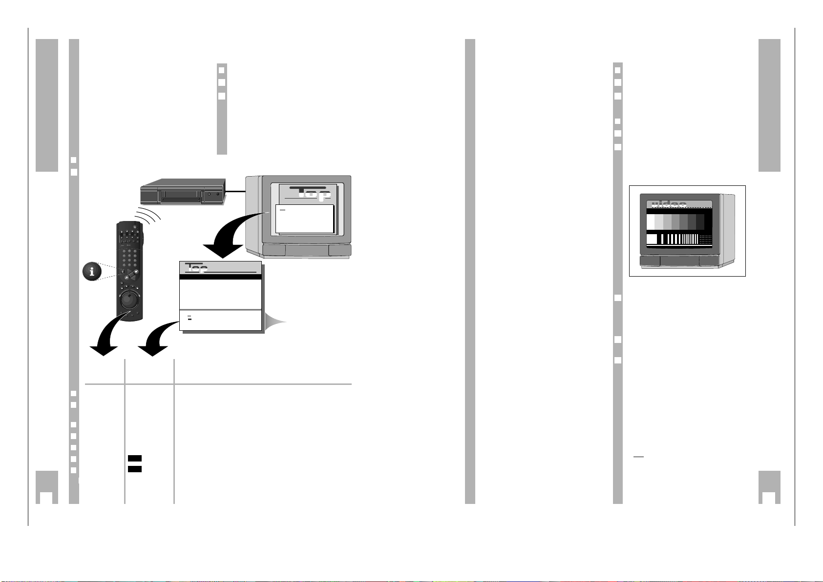
Allgemeiner Teil / General GV 54…, GV 56…, SE 5106…
1 - 16 GRUNDIG Service
6
The User Guide
GRUNDIG user guide on the screen
of the television set
… offers a dialogue between you and the recorder.
The recorder responds to many functions you sel-
ect with the remote control by displaying info tables
and dialogue lines on the screen of the TV set.
Button symbols for the remote control and dialogue
lines indicate the next operating step and available
options.
You are guided step by step, simply and understandably.
❒
Preparation
Switch the television set on.
Select the programme position for the video recor-
der at the TV set (AV programme position).
w
!
If the recorder is connected to a television set with
Megalogic function, the TV set switches itself on
and selects the AV programme position automatically when you press the h button.
w
!
The info table can be enlarged using the
¢
<
button.
2
1
Button on the Representation in Function
remote control the info table and
the dialogue lines
❒
h i
Calls up the info table and switches back to the TV picture.
❒
1 2 … 90 0-9
For selecting various functions from the info table;
for entering data directly.
❒
DC % &
For step-by-step selection of functions or lines in a table.
❒
FE " !
For switching between tables, for selecting data, and for altering settings.
❒
B
+/
–
For step-by-step entering of data for TIMER recording.
❒
Z
VPS (red)
Switches the VPS/PDC control of a TIMER recording off and back on.
❒
Z
ED/EW (green)
Selects a “daily” or “weekly” recording during TIMER programming.
❒¢
SP/LP ¢CLEAR
LP/CL
SP/LP: Switches to long-play mode and back to standard-play mode.
CL: Deletes TIMER data.
❒
Calling up the info table
Press the h button on the remote control.
1
GRUNDIG
TEXT-PROGRAMMING
Info
1 : Record Programming
2 : A1/A2 Record Prepared
3 : Teletext
4 : Special Functions
5 : Installation
■ 10 CNN 01. 15:00 16:30
■
■
■
■
■
+/– : Enter timer data
: VPS/PDC On/Off
: ED/EW Normal
LP/CL :Long Play/Clear timer
CHECK :next timer
i :Return to Info menu
Timer Prog. Date Start Stop
dialogue lines
7
Settings
Tuning the TV set to the recorder
The TV set receives programmes from different stations on certain channels.
The recorder also transmits on such a channel (between channels 30 and 40 ± 2 channels in the UHF
band) to which the TV set must now be tuned.
A “transmitter” is installed in the recorder to assist
you in finding this channel.
w
!
This adjustment is not necessary if the recorder and
the TV set are connected with a EURO-AV cable
(see chapter “Connecting” on page 3).
If this is the case, switch the recorder’s transmitter
off to prevent picture interference (see page 8).
❒
Preparation
Switch the TV set on.
Select the programme position for the video recor-
der at the TV set (AV programme position).
❒
Tuning
Press C button.
Pull out the aerial cable from the socket
–II–
on the
recorder.
w
!
Make sure there is no cassette in the recorder.
– After a short time the recorder will “transmit” the
test pattern.
– Display on recorder: »
TEST
«.
Search and store the recorder test pattern at the TV
set – between channels 30 and 40 ± 2 channels in
the UHF band.
– Follow the instructions in the TV set operating
instructions.
Insert the aerial cable into the aerial socket
–II–
on
the recorder.
If the picture quality is good, terminate setting
using the A button.
w
!
If the picture quality is poor, proceed as described
in the chapter “Improving picture quality” on the
next page.
w
!
If the recorder is connected to a TV set with 100Hz
technology, and if the test pattern “skips” or “shivers”, the recorder must be adjusted.
One after another, press the
¢
CODE button, the
numbered buttons 8547 and the G but-
ton on the remote control.
– Brief display on the recorder: »ON«.
If after this adjustment has been made the recorder
is connected to a conventional TV set with 50Hztechnology, press the
¢
CODE button, numbered
buttons 8546 and the G button one
after another.
– Brief display on the recorder: »
OFF
«.
5
4
3
GRUNDIG CTI TEST PATTERN
No reception of Programme 01
GRUNDIG
PATTERN
2
1
2
1
➡
DAY START
STOP
PROG.
ON/OFF
SP/LP
CLEAR
SV/V+
SET/CHECK
TIMER
2
3
1
5
6
4
8
9
7
0
AVVPT
+
+
OK
-
I
G
N
N
I
D
K
E
C
X
A
R
T
IN
D
E
E
S
X
A
R
M
E
A
X
R
E
K
D
I
N
e
TIMER
ON/OFF
%
%
GRUNDIG
TEXT-PROGRAMMING
Dialogzeilen
Page 15

GV 54…, GV 56…, SE 5106… Allgemeiner Teil / General
GRUNDIG Service 1 - 17
8
Settings
❒
Improving picture quality
If wavy lines are visible on the TV screen, the channel tuned to is already occupied by a TV station.
In this case, proceed as follows:
Press C button.
On the TV set, search for a channel – in the UHFband between channels 30 and 40 ± 2 channels –
that is not occupied by a TV station (only snow on
the screen).
Store the channel at the TV set (see operating
instructions for the TV set).
Pull the aerial cable out of the socket
–II–
on the
recorder.
w
!
Make sure there is no cassette in the recorder.
– After a short time the recorder will “transmit” the
test pattern.
Using a screwdriver of appropriate size, turn the
channel selector q on the back of the recorder (see
illustration) to the left or to the right until the test
pattern appears on the TV screen.
Re-insert the aerial cable into the socket
–II–
on the
recorder.
Terminate setting by pressing the button A .
7
6
L
H
L
H
x
x
+
+
–
–
5
4
3
2
1
❒
Switching the recorder’s transmitter off
and on
If your recorder receives many TV stations between
the channels 30 and 40 in the UHF band, you may
experience picture interference when using your
recorder. To avoid this, the recorder’s transmitter
may be switched off.
w
!
In order for the picture/sound signal of the recorder
to be passed to the TV set, the two units must be
connected with a EURO-AV cable (see page 3).
Switch the recorder´s transmitter off by pressing
the
¢
CODE button, the numbered buttons
8518and the G button in sequence.
– The recorder´s transmitter is switched off.
– Brief display at recorder: »
OFF
«.
Switch the recorder´s transmitter on by pressing
the
¢
CODE button, the numbered buttons
8519and the G button in sequence.
– The recorder´s transmitter is switched on.
– Brief display at recorder: »ON«.
2
1
Tuning TV stations
Television stations broadcast programmes on different frequencies/channels.
The recorder has a built-in receiver for receiving
and recording television programmes independently of the TV set.
First you must tune your recorder to the channels
used by the different TV stations.
There are 99 programme positions available. You
can assign them as you wish to TV stations from
the aerial, a cable connection or a satellite.
❒
A number of options are available
for tuning:
1. By transfer of data from the TV set.
The TV set must be equipped with Megalogic
functions.
2. With the automatic tuning system (ATS euro
plus). The recorder searches, sorts, and stores
all channels/special channels which it can receive
at its location.
This procedure depends on the language and
country you select, as well as on the reception
quality of the TV stations.
If you are not satisfied with the order in which
the TV stations are allocated, you can change the
order later.
3. By entering data directly.
4. By searching manually, for example if there are
new TV stations, or if the recorder could not find
a TV station using the automatic tuning system.
❒
Notes concerning TIMER programming
using the teletext pages of the TV
stations.
For this type of TIMER programming you take the
data for the broadcast (for example programme,
date, switch-on and switch-off times) from the programme overviews that certain TV stations provide
in the teletext pages, rather than from a programme
guide magazine.
The page numbers of the teletext pages on which
the programme overviews are found can vary from
station to station.
Now you can decide which page of the programme
overview contains the most recordings you wish to
program.
Enter the number of the required teletext page in
the »TV Station Table«.
The following pages explain how to do this.
This teletext page will then be called up automatically during VPT programming.
Transfer of data from the TV set
(Megalogic function)
If the recorder is connected to a TV set with Megalogic function, the recorder automatically accepts
the TV stations stored in the TV set.
To enable the recorder to do this, you must carry
out the following steps in the order indicated.
w
!
Recorder and TV set must be connected with the
Megalogic EURO-AV cable provided with your
recorder, and the TV set must be switched on.
Remove the plug for the recorder from the mains.
Re-insert the plug for the recorder into the mains.
– The recorder automatically takes the TV program-
mes from the TV set. .
Thus the recorder will have the same programme
position assignments as the TV set.
2
1
9
Settings
➡➡
Page 16
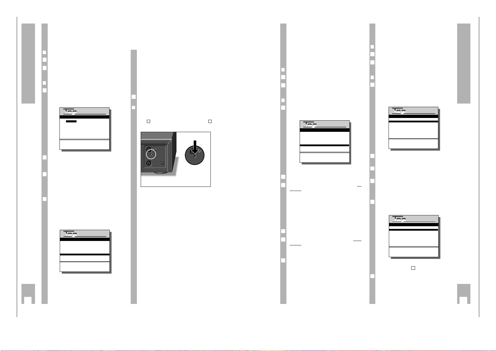
Allgemeiner Teil / General GV 54…, GV 56…, SE 5106…
1 - 18 GRUNDIG Service
Tuning TV stations using the
automatic channel search and
memory system (ATS euro plus)
❒
Preparation
Switch the TV set on.
Select the programme position for the video recor-
der at the TV set (AV programme position).
❒
Example
Select the search function by pressing the h but-
ton and then the numbered buttons 5 and 1 one
after another.
– The »Select language« table appears.
Select the language of your location using the
FE DCbuttons and confirm using the G
button.
Select the country (location) using the F E DC
buttons and confirm using the G button.
w
!
If the country you require is not in the table, select
the »??« line.
Start the automatic channel search using the G
button.
– Display on the recorder: »
ATS
« and »A«.
– The recorder searches all channel numbers for TV
stations, sorts and stores them.
– After completion of the search the » TV Station
Table« appears.
w
!
The station identification for TV stations which broadcast a VPS/PDC signal is inserted automatically
in the »TV Station Table«.
4
3
2
1
2
1
10
Settings
Deutsch Portuguêse
Español Svenska
Français Norsk
English Dansk
Italiano Suomi
Nederlands
<
&
%
>:Select
OK :Confirm
i : Return to Info menu
Select language
Prog. Channel Ident VPT
k
11 06 ARD 304 150
12 34 ZDF 304 150
13 59 BR 3 304 150
14 40 RTL 303 150
15 36 SAT 1 303 150
16 21 PRO 7 100 150
17 53 ----- 100 150
18 56 ----- 100 150
19 24 ----- 100 150
10 - <&%>:Select programme
■
: Sort/copy station
OK :Change programme settings
CLEAR :Delete station
i : Return to Info menu
TV Station Table
w
!
For broadcasts that do not send a VPS/PDC signal,
» Ident -----«, »VPT 100« and »k 150« appear in
the »TV Station Table«, and the programme position is marked in blue.
The example on page 12 explains how you can
enter this data.
w
!
In the examples on the next pages you can read
how to change the order of TV programmes, enter
data manually or delete data.
Terminate setting with the
¢
8
button.
❒
Eliminating picture interference
If the recorder does not carry out the ATS euro plus
search correctly, shift the attenuator switch to position and repeat the setting starting with step
of the example.
L
H
L
H
x
x
+
+
–
–
L
H
L
H
1
H
5
➡
Resorting TV stations –
manually
❒
Preparation
Switch the TV set on.
Select the programme position for the video recorder
at the TV set (AV programme position).
❒
Example
Select »TV Station Table« by pressing the h button
and the numbered buttons 5 and 3 one after another.
– The »TV Station Table« appears, the selected pro-
gramme position is marked.
Select programme position using the DC E F
buttons.
Mark programme position with the Z ED/EW (green)
button.
Select new programme position with the DC buttons.
– The data for the marked programme position are
transferred to the new programme position.
Store setting using the G button.
– The subsequent TV stations are moved by one
position.
To resort additional TV programmes, repeat the procedure starting at step .
End the setting procedure using the
¢
8
button.
6
2
5
4
3
2
1
2
1
Resorting TV stations – with the
Follow TV function
Here the recorder receives the same programme
position assignment as the TV set.
w
!
The recorder and the TV set must be connected
with a EURO-AV cable.
❒
Preparation
Switch the TV set on.
Select the programme position for the video recor-
der at the TV set (AV programme position).
❒
Example
Select the Follow TV function by pressing the h
button and then the numbered buttons 5 and 2
one after another.
– Display at recorder: »
SELECT TV POI
«.
Select programme position 1 at the TV set.
Press the G button on the remote control of the
recorder.
– Display on recorder: »
PLEASE WAIT
«.
– The recorder “searches” for the data of the first
programme position of the TV set. It fills its first
programme position with the same TV station as
is on the TV set.
– When this procedure has been completed, the fol-
lowing display appears on the recorder:
»
SELECT TV PO2
«.
Select programme position 2 at the TV set.
Press the G button on the remote control of the
recorder.
– Repeat the setting until all TV stations have been
sorted.
End the setting procedure using the
¢
8
button.
w
!
Assignment errors can occur if two TV stations are
broadcasting the same programmes.
Repeat the setting when the stations are broadcasting different programmes.
6
5
4
3
2
1
2
1
11
Settings
Prog. Channel Ident VPT
k
11 06 ARD 304 150
12 34 ZDF 304 150
13 59 BR 3 304 150
14 40 RTL 303 150
15 36 SAT 1 303 150
16 21 PRO 7 100 150
17 53 NTV 100 150
18 56 ----- 100 150
19 24 ----- 100 150
10 - <&%>:Select programme
■
: Sort/copy station
OK :Change programme settings
CLEAR :Delete station
i : Return to Info menu
TV Station Table
➡
Prog. Channel Ident VPT
k
11 06 ARD 304 150
12 34 ZDF 304 150
13 59 BR 3 304 150
14 40 RTL 303 150
15 36 SAT 1 303 150
16 21 PRO 7 100 150
17 53 ----- 100 150
18 56 ----- 100 150
19 24 ----- 100 150
10 - -
<&%> : Select programme
■
: Sort stations
OK :Change programme settings
CLEAR :Delete station
i : Return to Info menu
TV Station Table
Prog. Chan. Ident VPT
k
11 06 ARD 304 150
12 34 ZDF 304 150
13 59 BR 3 304 150
14 21 PRO7 100 150
15 36 SAT 1 303 150
16 40 RTL 303 150
17 53 NTV 100 150
18 56 ----- 100 150
19 24 ----- 100 150
10 - -
<
&
%
>:Select programme
■
: Sort/copy station
OK :Change programme settings
CLEAR :Delete station
i : Return to Info menu
TV Station Table
GRUNDIG
ATS euro plus
GRUNDIG
ATS euro plus
GRUNDIG
TEXT-PROGRAMMING
GRUNDIG
TEXT-PROGRAMMING
GRUNDIG
TEXT-PROGRAMMING
Page 17
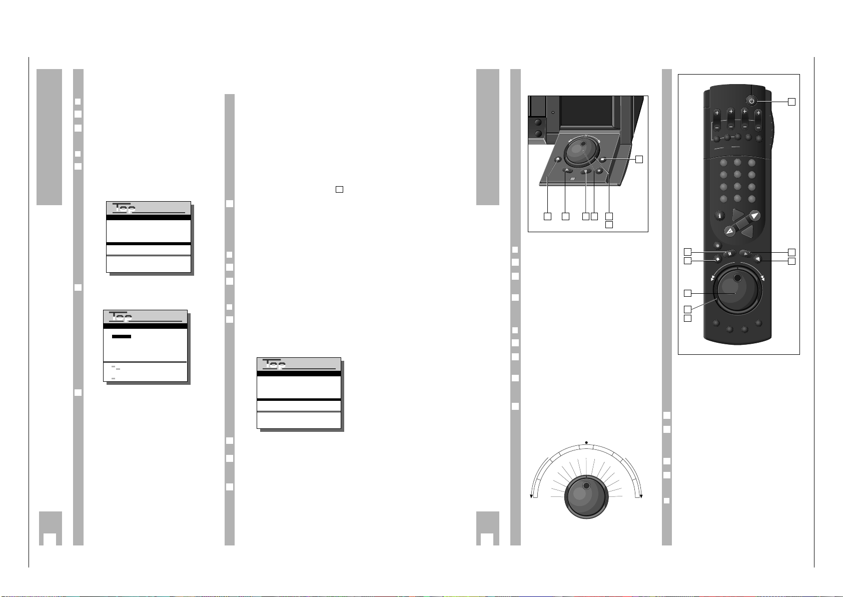
GV 54…, GV 56…, SE 5106… Allgemeiner Teil / General
GRUNDIG Service 1 - 19
Entering data manually
❒
Preparation
Switch the TV set on.
Select the programme position for the video recor-
der at the TV set (AV programme position).
❒
Example
Call up the » TV Station Table« by pressing the h
button and then the numbered buttons 5 und 3
one after another.
– The » TV Station Table « appears, the selected
programme position is marked.
Use the DC E F buttons to select the programme position, then press G button.
– The »Programme« table appears.
Select data line using the DC buttons.
The texts mean:
Sat – Satellite TV programme (the set-
ting »Sat: Yes« can only be selected if an external satellite receiver is connected to the EURO-AV
DECODER A2 socket).
Channel – the channel number or fre-
quency of the TV station,
Name – the station identification
(max. 5 places),
Norm – PAL or SEC colour norm,
Decoder – activate programme position
for external decoder,
Fine Tuning – fine tuning of picture,
Teletext page – the number of the page,
Subtitle page – the number of the page.
w
!
For further operating steps please see the dialogue
lines of the »Programme« table.
3
2
1
2
1
w
!
For satellite TV programmes, enter the station identification and the number of the teletext page at the
same programme position as in the satellite
receiver.
No additional settings are possible.
w
!
Alternatively, the frequency of the TV programme
can be entered instead of the channel number, or an
automatic channel search can be started.
w
!
The » TV Station Table« appears again after confirmation of the subtitle page number.
To enter data for the next programme position,
repeat the procedure starting from step .
End the setting procedure with the
¢
8
button.
Deleting the data for a programme
position
❒
Preparation
Switch the TV set on.
Select the programme position for the video recor-
der at the TV set (AV programme position).
❒
Example
Call up the » TV Station Table« by pressing the h
button and then the numbered buttons 5 and 3
one after another
– The » TV Station Table « appears, the selected
programme position is marked.
Select the programme position with the DC
EFbuttons.
Delete the data line with the
¢
CLEAR button.
– The subsequent TV stations are shifted up one
programme position.
End the setting procedure with the
¢
8
button.
4
3
2
1
2
1
4
2
12
Settings
Sat: No
Channel C
■
39
Name: -----
Norm: PAL
Decoder: OFF
Fine Tuning: -3
Teletext page: 301
Subtitle page: 320
0-9/< > : Enter channel/search
: Special channel On/Off
:
Frequency/Channel-Input
&
%
: Select
OK : Confirm
: TV-Picture
Programme 12
Prog. Channel Ident VPT
k
11 06 ARD 304 150
12 34 ZDF 304 150
13 59 BR 3 304 150
14 40 RTL 303 150
15 36 SAT 1 303 150
16 21 PRO 7 100 150
17 53 ----- 100 150
18 56 ----- 100 150
19 24 ----- 100 150
10 - -
<
&
%
>:Select programme
■
: Sort/copy station
OK :Change programme settings
CLEAR :Delete station
i : Return to Info menu
TV Station Table
Prog. Channel Ident VPT
k
11 06 ARD 304 150
12 34 ZDF 304 150
13 59 BR 3 304 150
14 40 RTL 303 150
15 36 SAT 1 303 150
16 21 PRO 7 100 150
17 53 ----- 100 150
18 56 ----- 100 150
19 24 ----- 100 150
10 - -
TV Station Table
<
&
%
>:Select programme
■
: Sort/copy station
OK :Change programme settings
CLEAR :Delete station
i : Return to Info menu
❒
Preparation
Switch the TV set on.
Select the programme position for the video recor-
der at the TV set (AV programme position).
Insert a recorded cassette into the cassette slot.
The video recorder automatically determines the
playing time of the cassette.
❒
Operation
Start playback with the T button.
Select pause/freeze-frame by pressing the W
button.
Advance the freeze-frames forwards/backwards one
by one by turning the jog dial to the left or right
during playback pause.
Select various forward/backward playback speeds
by turing the shuttle ring to the left or right during
playback.
The figure illustrates the possibilities.
2 times
5 times
7 times
11 times
5 times
7 times
11 times
1/2
1/12
1/2
1/12
+
–
0
11
S
l
o
w
N
o
r
m
a
l
F
a
s
t
F
r
e
e
z
e
S
e
a
r
c
h
Sl
o
w
N
o
r
m
al
F
a
s
t
S
e
a
r
c
h
P
la
y
b
a
c
k
f
o
r
w
a
r
d
P
l
a
y
b
a
c
k
r
e
v
e
r
s
e
3 times
4
3
2
1
3
2
1
w
!
The slow motion speed can be changed during slow
motion using the jog dial.
w
!
To return to normal playback from playback function pause/freeze-frame and the other playback functions, press the T button.
End playback using the H button.
To fast-forward or rewind the tape, turn the shuttle
ring to the right or left while in the stop function.
Terminate fast winding using the H button.
Remove the cassette by pressing N .
Switch the recorder off using the A button on the
remote control.
❒
Megalogic function
If the recorder is connected to a TV set with Megalogic functions, the TV set switches itself on after
playback is started and automatically switches to
the AV programme position.
8
7
6
5
14
Playback
%
%
➡
At a glance
17
8
1
7
2
5
4
3
6
2 3 4
6
5
GRUNDIG
TEXT-PROGRAMMING
GRUNDIG
TEXT-PROGRAMMING
GRUNDIG
TEXT-PROGRAMMING
DAY START
ON/OFF
STOP
SP/LP
SV/V+
2
3
5
6
8
9
0
AVVPT
+
+
PROG.
CLEAR
SET/CHECK
TIMER
1
4
7
OK
-
I
N
D
E
X
IN
D
E
X
M
R
T
E
S
A
R
E
A
X
R
E
K
D
I
N
G
N
I
K
C
A
Page 18

Allgemeiner Teil / General GV 54…, GV 56…, SE 5106…
1 - 20 GRUNDIG Service
Additional playback functions
❒
Playback of long-play recordings
The recorder automatically switches to long-play
playback mode when playing back a long-play
recording.
– Display on recorder: »LP«
w
!
Picture disturbances may occur during long-play
operation.
❒
Playback of recordings with other colour
norms
SECAM colour nor
m
Press the
¢
PAL/SEC button to play back SECAM
recordings
– Display on recorder: »
SEC
«.
w
!
The TV set must also correspond to this colour
norm.
After playback, press the
¢
PAL/SEC button again;
the »
SEC
« display disappears.
NTSC colour norm
The recorder automatically switches to the NTSC
system when playing back NTSC recordings.
– Brief display on the recorder: »
NTSC
«.
»
NTSC SP
« (Standard Play) or
»
NTSC EP
« (Extended Play).
w
!
The total playing time display changes to a five-digit
tape length display.
w
!
The freeze-frame function is not possible during
NTSC playback.
w
!
Picture disturbances may occur during NTSC longplay mode playback.
❒
Playback of S-VHS recordings
The recorder automatically switches to the S-VHS
system when playing back recordings that were
recorded using this format.
– Display on the recorder » «.
❒
Selecting the audio track
The desired audio track can be selected when playing back recordings with stereo or two-channel
sound.
The basic setting is stereo (hifi helical track)
– Display on the recorder: »)« and »
STEREO
«.
Pressing the
¢
AUDIO
button repeatedly selects the
following settings:
Audio track 1 –
Display on recorder: »I« and
»
LEFT
«;
Audio track
2 – Display on recorder: »2« and
»
RIGHT
«.
Mono/longitudinal track – without display;
Mixed mode (hifi helical track and mono/longitudinal track, for checking dubbed cassettes)
– Display on recorder: »
MIX
«.
Adjusting picture/sound quality
❒
Picture/sound quality adjustment –
automatic
After a cassette has been inserted and playback has
started, the recorder automatically adjusts for the
best possible picture quality (Auto Tracking).
– During adjustment, the recorder display shows
»
AUTO-TRACK
« and the picture/sound quality
may change.
❒
Picture/sound quality adjustment –
manual
Press the
¢
TRACKING button.
– Display on recorder: »
TRACKING
«.
Use the
F E
buttons on the remote control to
carry out the tracking adjustment.
Store the tracking adjustment with the Gbutton.
❒
Optimizing the picture/sound quality for
cassettes recorded on another recorder
If the picture jumps or scrolls when playing back
tapes recorded on another recorder, press the
¢
CODE button, the numbered buttons
8511
and the G button one after another.
– Brief display on the recorder: »ON«.
❒
Optimizing the picture/sound quality for
special playback functions
If the picture jitters or appears uneven during the
playback functions freeze-frame, slow motion forward or playback 2x forward, the picture can be
optimized.
During playback, one after another, press the
h button the numbered button 2 and the
G
button.
– Display on the recorder: »
JITTER
«.
Adjust the picture to suit your personal taste using
the
D or C
buttons. Then press the Gbutton.
❒
Optimizing the picture definition
(Crispening)
Automatic
(Automatic Contour Control)
The recorder automatically adjusts to the optimum
picture definition after the cassette has been inserted and playback begins.
Manual
During playback the DCbuttons can be used to
adjust the picture definition to suit your personal
taste.
– Brief display on the recorder:
»
SHARPNESS + I
«.
2
1
3
2
1
15
Playback
➡
❒
Preparation
Switch the TV set on.
Select the programme position for the video recor-
der at the TV set (AV programme position).
Insert a cassette of sufficient length into the casset-
te compartment.
❒
Operation
Select a programme position, step-by-step with the
DC buttons on the remote control or the c d
buttons on the recorder;
directly with the numbered buttons 1 ... 0 on the
remote control.
w
!
For two-digit programme positions, press the numbered buttons briefly one after another.
Select long-play recording – if desired – using the
¢
SP/LP button on the remote control.
– This doubles the playing time of the cassette.
Start recording with the K button.
Select recording pause using the W button.
Resume recording with the K button.
Terminate recording with the H button.
Fast-forward or rewind tape by turning the shuttle
ring to the left or right while recorder is in stop
function.
Terminate fast winding with the H button.
Remove cassette by pressing the N button.
Switch the recorder off using the A button on the
remote control.
8
7
6
5
4
3
2
1
3
2
1
❒
Megalogic function
If the recorder is connected to a TV set with Megalogic functions, it is possible to record the TV
programme which is visible on the TV screen by
pressing the K button.
The programme position need not be selected on
the recorder.
17
Recording
➡
At a glance
8
7
4
5
6
3
2
1
1
3
7
1
4 6
5
%
%
DAY START
ON/OFF
STOP
SP/LP
SV/V+
2
3
5
6
8
9
0
AVVPT
+
+
OK
PROG.
CLEAR
SET/CHECK
TIMER
1
4
7
-
I
N
D
E
X
IN
D
E
X
M
T
E
S
A
R
E
A
X
R
E
K
D
I
N
G
N
I
K
C
A
R
Page 19

GV 54…, GV 56…, SE 5106… Allgemeiner Teil / General
GRUNDIG Service 1 - 21
Selecting the language for the
user guide
The language for the user guide can be changed.
This change has no effect on the setting of the TV
programmes with the ATS euro plus automatic
channel search.
❒
Preparation
Switch the TV set on.
Select the programme position for the video recor-
der at the TV set (AV programme position).
❒
Operation
One after another, press the h button and the
numbered buttons 5 und 4.
– The »Select language« table appears
– The selected language is indicated in colour.
Select the desired language using the DC F E
buttons and confirm using the G button.
– The recorder switches to the TV picture. From
now on, all info tables and dialogue lines will
appear in the selected language.
2
1
2
1
38
Special Functions
Checking/Setting
the time and date
w
!
The digital clock continues to operate even if the
recorder is separated from the mains (the time is
not displayed).
❒
Automatic adjustment
The clock is automatically adjusted during teletext
operation with programme position 1.
❒
Manual adjustment
❒
Preparation
Switch the TV set on.
Select the AV programme position for the video
recorder at the TV set (serves as monitor).
❒
Operation
One after another, press button h and then the
numbered buttons 5 and 5.
– The »Set Time/Date « table appears.
Enter the time as a four-digit number using the
numbered buttons 1 … 0.
Use the D button to select the » Date « line and
enter the date as a six-digit number using the
numbered buttons 1 … 0.
Store the entry using the G button.
End the setting procedure using the h button.
5
4
3
2
1
2
1
Time:❚8:00
Date: 02.03.95
0-9 :Enter time
%
: Select time
OK :Store date and time
i :Return to Info menu
Set Time/Date
Deutsch Portuguêse
Español Svenska
Français Norsk
English Dansk
Italiano Suomi
Nederlands
<
&
%
>:Select
OK :Confirm
i :Return to Info menu
Select language
39
Special Functions
Remote control of other GRUNDIG
video recorders
Different GRUNDIG video recorders can be operated independently of one another using this remote
control.
Your GV 560 and a second video recorder from the
VS 600 to VS 900 series and from the GV 200
series on.
The GV 560 must be reset so that it can receive the
remote control commands properly.
❒
Setting the VCR address for the GV 560
One after another, press the h buttton and the
numbered buttons 4 and 4.
– The »VCR address« table appears.
Select VCR address 2 with the FEbuttons.
Confirm the setting with the G button.
– The recorder switches the table off.
❒
Remote control of the two recorders
With the switch in the VIDEO 2 position you can
operate the GV 560;
With the switch in the VIDEO 1 position you can
operate the second recorder.
w
!
If the VIDEO 1 2 switch is not at the selected VCR
address during GV 560 operation, the display
»
VID I
« or »
VID 2
« on the recorder signals that
the remote control must be switched to the other
VCR address.
1
2
TV
1
2
TV
SP/LP
ON/OFF
CLEAR
SV/V+
STOP
TART
9
3
6
2
2
1
3
2
1
Remote control of the TV set
This video remote control enables you to operate
GRUNDIG colour TV sets that use remote control
model TP 590 or higher.
w
!
Which functions you will actually be able to use
depends on the features of the particular GRUNDIG
TV equipment.
❒
Preparation
Switch on the TV set using the mains switch.
Shift the switch on the remote control to TV position.
w
!
Direct the remote control towards the TV set.
❒
Operation
The programme positions can be advanced stepby-step from 1 to 99 using the DC buttons.
The programme positions can be selected directly
using the numbered buttons 1 … 0.
The programme positions A1, A2 etc. can be selected by repeatedly pressing the e button.
Adjusting the volume.
Press the F button to decrease the volume.
Press the E button to increase the volume.
Stand-by
During pauses in TV viewing the TV set can be kept
at stand-by using the A button.
Press the e button to switch the TV set on again.
3
2
1
1
2
TV
1
2
TV
SP/LP
ON/OFF
CLEAR
SV/V+
STOP
ART
9
3
6
2
2
1
VCR address 1
<>:Select VCR address 1/2
OK :Confirm
i :Return to Info menu
VCR address
VIDEO 1
VIDEO 2
TV
VIDEO 1
VIDEO 2
TV
GRUNDIG
TEXT-PROGRAMMING
GRUNDIG
TEXT-PROGRAMMING
GRUNDIG
TEXT-PROGRAMMING
Page 20
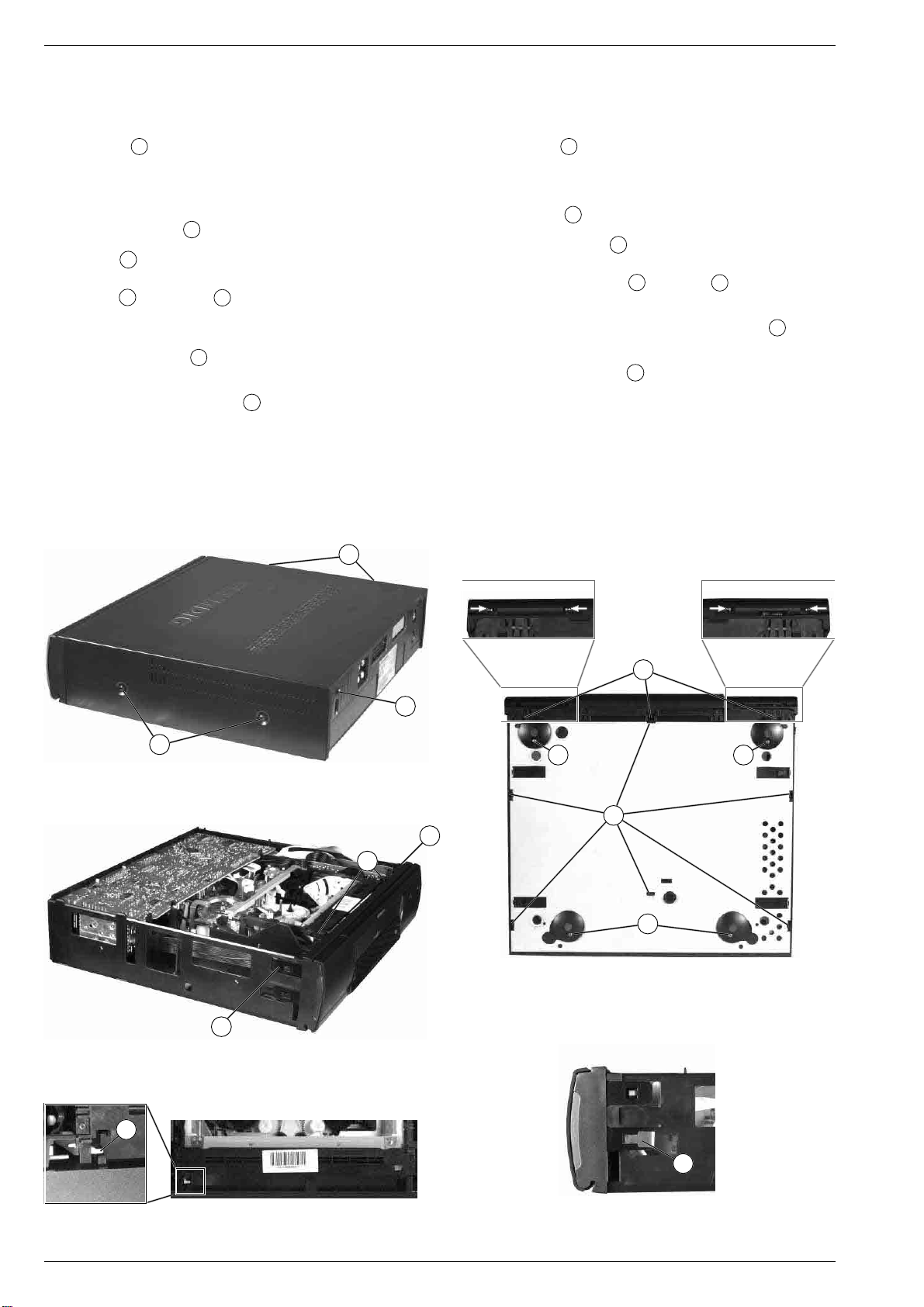
Allgemeiner Teil / General GV 54…, GV 56 …, SE 5106…
Servicehinweise
1. Entfernen der Gehäuseteile
1.1 Gehäuseoberteil
– 5 Schrauben A herausdrehen (Fig. 1).
– Seitenteile des Gehäuseoberteils vorsichtig etwas auseinander-
ziehen und dabei Gehäuseoberteil ca. 3cm nach hinten schieben
und abnehmen.
1.2 Bodenblech
– Befestigungsschraube B je Gerätefuß herausdrehen (Fig. 2).
– Gerätefuß abnehmen.
– Rastnasen C lösen (Fig. 2) und Bodenblech abnehmen.
1.3 Frontblende
– Rasthaken D (Fig. 3) sowie E (Fig. 2) lösen, Frontblende abneh-
men und gegebenenfalls Steckverbindung lösen.
Hinweis zum Zusammenbau: Beim Aufstecken der Frontblende
von vorne auf das Gerät ist die Cassettenklappe so nach innen zu
drücken, daß der Hebel F in die Führung (Fig. 4) der Cassettenklappe eintaucht.
Bei Geräten mit Bedienelementen in der Frontklappe (links bzw.
rechts) muß je die Massefeder(n) G angebracht sein (Fig. 5).
1.3.1 Frontklappen
– Frontblende abnehmen und gegebenenfalls Steckverbindungen lösen.
– Scharnierstifte (2 je Frontklappe) in die angegebenen Richtungen
schieben (Fig. 2).
– Frontklappen halb öffnen und abnehmen.
Service Instructions
1. Removing the Cabinet Parts
1.1 Cabinet Upper Part
– Undo 5 screws A (Fig. 1).
– Pressing the side panels carefully apart push the upper part of the
cabinet towards the rear by approx. 3cm and remove it.
1.2 Bottom Panel
– Undo the screw B of each foot (Fig. 2).
– Take off the foot.
– Release the locking lugs C (Fig. 2) and remove the bottom panel.
1.3 Front Panel
– Release the locking catches D (Fig. 3) and E (Fig. 2), remove the
front panel and unplug the connector if necessary.
Note: When attaching the front panel from the front to the video
recorder press the cassette lid inwards so that the lever F engages
with the guide (Fig. 4) of the cassette lid.
On VCRs the front flap (left or right) of which is fitted with operating
elements the earth spring(s) G must be inserted as shown in Fig. 5.
1.3.1 Front Flaps
– Remove the front panel and unplug the connectors if necessary.
– Push the hinge pins (two for each flap) in the direction of the arrows
(Fig. 2).
– Open the front flaps halfway and remove them.
A
E
A
A
Fig. 1
D
D
B
C
B
Fig. 2
B
D
Fig. 3
F
G
Fig. 4
1 - 22 GRUNDIG Service
Fig. 5
Page 21
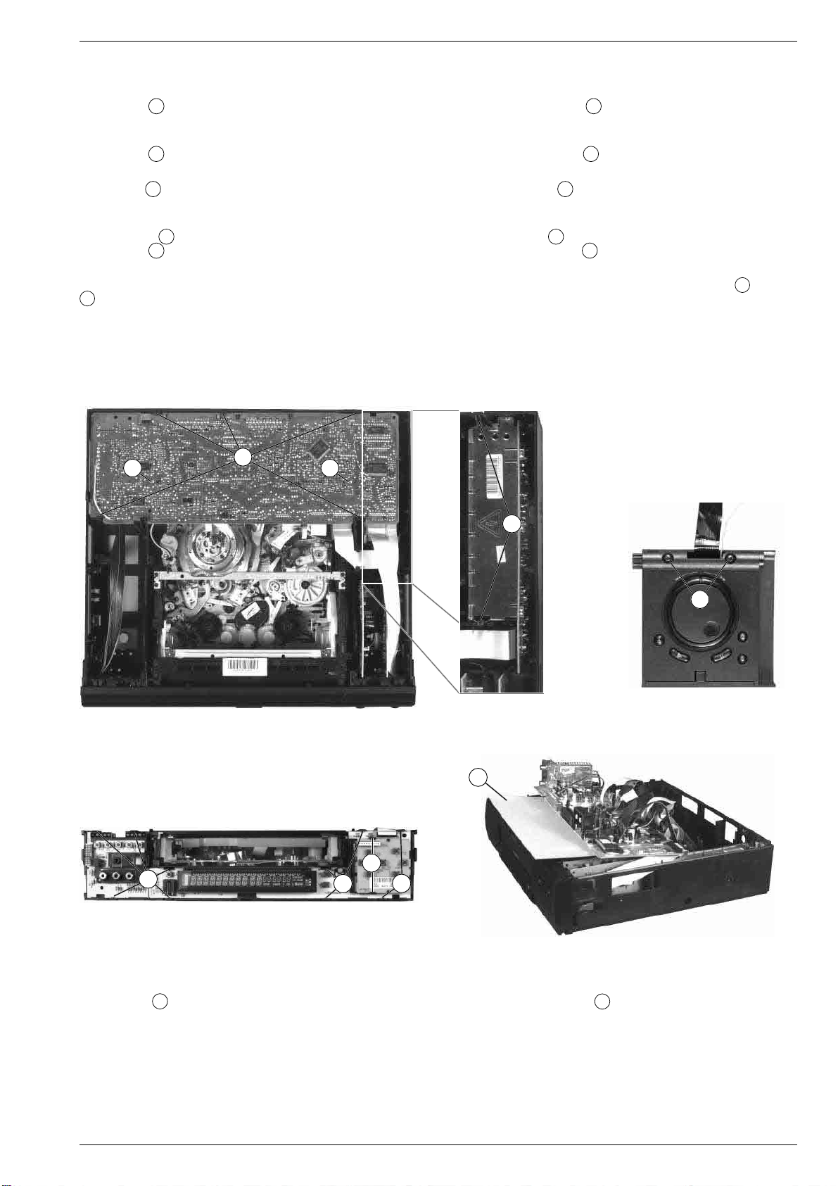
GV 54…, GV 56 …, SE 5106… Allgemeiner Teil / General
2. Ausbauhinweise
2.1 Bedieneinheit I ausbauen
– Rastnasen I lösen (Fig. 9) und Bedieneinheit I abnehmen.
– Gegebenenfalls Steckverbindung lösen.
2.1.1 Bedieneinheit II (auf der Bedieneiheit I – Fig. 9) ausbauen
– Rastnasen J lösen (Fig. 10) und Bedieneinheit II abnehmen.
2.1.2 Bedieneinheit II (in der Frontklappe – Fig. 8) ausbauen
– Schrauben K herausdrehen (Fig. 8).
– Jog/Shuttle-Drehknöpfe abziehen und Bedieneinheit II abnehmen.
2.2 Chassisplatte ausbauen
– 2 Schrauben L herausdrehen (Fig. 6).
– Rastnasen M lösen und Chassisplatte herausnehmen (Fig. 6).
– Gegebenenfalls Steckverbindungen lösen.
Servicestellung: Chassisplatte mit einer nichtleitenden Unterlage
X
auf das Laufwerk legen (Fig. 10).
Achten Sie nach dem Austausch darauf, daß…
…das EPROM IC7250 bestückt ist.
…das Verbindungskabel zwischen dem Tuner und dem Modulator
angeschlossen ist.
Führen Sie die Abgleichschritte gemäß Kapitel 3 durch.
L
M
L
2. Disassembly Instruction
2.1 Removing the Keyboard Unit I
– Release the locking lugs I (Fig. 9) and withdraw the Keyboard Unit I.
– Unplug the connector if necessary.
2.1.1 Removing the Keyboard Unit II (on the Keyboard Unit I – Fig. 9)
– Release the locking lugs J (Fig. 10) and withdraw the Keyboard Unit II.
2.1.2 Removing the Keyboard Unit II (at the Front Flap – Fig. 8)
– Undo the screws K (Fig. 8).
– Pull off the Jog/Shuttle rotary knobs and withdraw the Keyboard Unit II.
2.2 Removing the Family Board
– Undo 2 screws L (Fig. 6).
– Open the locking lugs M and take out the Family Board (Fig. 6).
– Unplug the connectors if necessary.
Service Position: Lying on a non-conducting material X place the
Family Board onto the tape deck (Fig. 10).
After replacement ensure that:
…the EPROM IC7250 is fitted.
…the connecting cable between the tuner and the modulator is
connected.
Carry out the alignment procedures described in chapter 3.
N
K
Fig. 6
J
I
I
I
Fig. 7 Fig. 8
X
Fig. 9
2.3 Netzteilbaustein ausbauen
– Rastnasen N ausrasten und Netzteilbaustein herausnehmen
(Fig. 7).
– Gegebenenfalls Steckverbindungen lösen.
2.3.1 Reparaturen im Netzteil
Bei Reparaturen des Netzteilbausteins Trenntrafo benutzen!
Sollen Bauteile im nicht netzgetrennten Teil des Netzteils ausgetauscht werden, müssen Sie den Abschirmdeckel abnehmen.
Nach der Reparatur darauf achten, daß der Abschirmdeckel des
Netzteilbausteins angebracht ist!
GRUNDIG Service 1 - 23
2.3 Removing the Power Supply Board
– Release the locking lugs N and take out the Power Supply Board
(Fig. 7).
– Unplug the connectors if necessary.
2.3.1 Repairs within the Power Supply Unit
Use an isolating transformer when repairing the Power Supply Unit!
For replacing components in the non-isolated section of the Power
Supply Unit remove the shielding cover.
On completion of the repairs take care that the shielding cover is
refitted to the Power Supply Unit!
Fig. 10
Page 22
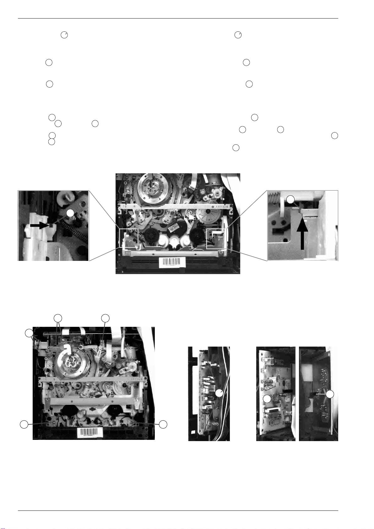
Allgemeiner Teil / General GV 54…, GV 56 …, SE 5106…
2.4 NICAM-Decoder ausbauen
– Führungsleisten N vorsichtig auseinanderdrücken und NICAM-
Decoder herausnehmen (Fig. 14)
– Gegebenenfalls Steckverbindungen lösen.
2.5 Teletextbaustein ausbauen
– Rastnase O (Fig. 15) lösen und Teletextbaustein herausnehmen.
– Gegebenenfalls Steckverbindungen lösen.
2.6 "Edit Control"-Baustein ausbauen
– Rastnase P (Fig. 16) lösen und "Edit Control"-Baustein heraus-
nehmen.
– Gegebenenfalls Steckverbindungen lösen.
2.7 Laufwerkausbau
– Chassisplatte ausbauen.
– Rasthaken Q (Fig. 13) lösen Laufwerkshalter herausnehmen.
– Arretierungen R (Fig. 11) und S (Fig. 12) des Cassettenschach-
tes lösen und diesen dabei so weit nach innen schieben, bis die
Schrauben U (Fig. 13) zugänglich sind.
– Schrauben U entfernen (Fig. 13) und gegebenenfalls Steckverbin-
dungen zur Elektronik lösen.
2.4 Removing the NICAM Decoder
– Press the guides N carefully apart and take out the NICAM
Decoder (Fig. 14).
– Unplug the connectors if necessary.
2.5 Removing the Teletext Board
– Release the locking lug O (Fig. 15) and take out the Teletext Board.
– Unplug the connectors if necessary.
2.6 Removing the Edit Control Board
– Release the locking lug P (Fig. 16) and take out the Edit Control
Board.
– Unplug the connectors if necessary.
2.7 Removing the Tape Deck
– Remove the Family Board.
– Release the locking catch Q (Fig. 13) and remove the tape deck
holder.
– Release the catches R (Fig. 11) and S (Fig. 12) of the cassette
compartment and move it inwards to gain access to the screws
U
(Fig. 13).
– Undo the screws U (Fig. 13) and unplug the connectors to the
electronics if necessary.
S
R
Fig. 11
Fig. 12
T U
Q
N
O
P
UU
Fig. 13
1 - 24 GRUNDIG Service
Fig. 15 Fig. 16Fig. 14
Page 23
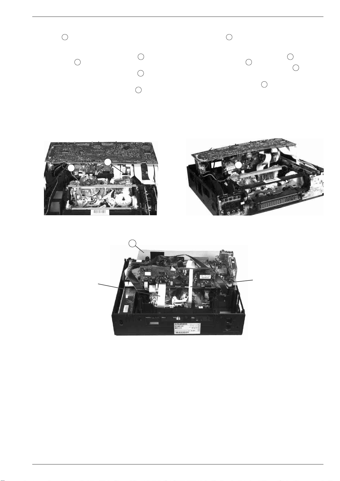
GV 54…, GV 56 …, SE 5106… Allgemeiner Teil / General
2.7.1 Chassisplatte II ausbauen
– Laufwerk ausbauen.
– Schrauben T (Fig. 13) herausdrehen, gegebenenfalls Steck-
verbindungen vorsichtig lösen und Chassisplatte II abnehmen.
Servicestellungen:
a)Chassisplatte II in die vorgesehenen Halterungen U stecken und
Masseverbindung V herstellen (Fig. 17).
Die Verbindungskabel zum Laufwerk sind dabei kontaktiert.
b)Chassisplatte II mit der Befestigungsschraube W am oberen
Platinenhalter des Laufwerks befestigen (Fig. 18).
Die Verbindungskabel zum Laufwerk sind dabei kontaktiert.
c) Chassisplatte mit einer nichtleitenden Unterlage X auf das Lauf-
werk legen (Fig. 10).
Chassisplatte II mit den langen Adapterkabeln (Fig. 19) kontaktieren. Das Verbindungskabel 1506 – L10 von der Chassisplatte II zur
Kopfscheibe ist nicht angeschlossen.
Die Chassisplatte II ist bei allen Laufwerksfunktionen (ohne Bild und
HiFi-Ton) von allen Seiten zugänglich.
U
V
2.7.1 Removing the Family Board II
– Remove the tape deck.
– Undo the screws T (Fig. 13), if necessary unplug the connectors
carefully and remove the Family Board II.
Service positions:
a)Insert Family Board II into the holding forks U provided and
connect the earthing cable V (Fig. 17).
b Secure the Family Board II with the fastening screw W to the upper
pcb holder of the tape deck (Fig. 18).
The connecting cables to the tape deck are connected.
c) Lying on a non-conducting material X place the Family Board onto
the tape deck (Fig. 10).
Connect the Family Board II with the long adapter cables (Fig. 19).
The connecting cable 1506-L10 from Family Board II to the headwheel is not connected.
The Family Board II is accessible from all sides during all tape drive
functions (without picture and HiFi sound).
W
Fig. 17
X
75988-010.78
3. Wichtige Masseverbindungen!
Beim Zusammenbau des Gerätes ist darauf zu achten, daß die
Masseverbindungen zwischen Gehäuseboden und Gehäuseoberteil,
Gehäuseboden und Netzteilbaustein, Bedieneinheiten der Frontklappen
und Gehäuseoberteil, Metallteile der Frontblende und Gehäuseoberteil
sowie Chassisplatte und Gehäuseoberteil gewährleistet sind.
Fig. 18
75988-031.20
Fig. 19
3. WARNING: Chassis Connections!
When re-assembling the machine it is strictly to be observed that the
chassis connections between the cabinet bottom and cabinet upper
part, cabinet bottom and Power Supply Board, Keyboard Control Units
at the front flaps and cabinet upper part, metal parts at the front panel
and upper part, Family Board and cabinet upper part are in good order.
4. Durchführen von Messungen
Bei Messungen mit dem Oszilloskop an Halbleitern sollten Sie nur
Tastköpfe mit 10:1 - Teiler verwenden. Außerdem ist zu beachten, daß
nach vorheriger Messung mit AC-Kopplung, der Koppelkondensator
des Oszilloskops aufgeladen sein kann. Durch die Entladung über das
Meßobjekt können diese Bauteile beschädigt werden.
5. Meßwerte und Oszillogramme
Bei den in den Schaltplänen und Oszillogrammen angegebenen
Meßwerten handelt es sich um Näherungswerte!
GRUNDIG Service 1 - 25
4. Carrying out Measurements
When making measurements on semi-conductors with an oscilloscope, only test probes with 10:1 dividing factor should be used.
Further, please note that if the previous measurement is made on AC
input, the coupling capacitor in the oscilloscope will be charged.
Discharge via the test object may damage these components.
5. Measured Values and Oscillograms
The measured values given in the circuit diagrams and oscillograms
are approximates!
Page 24
Allgemeiner Teil / General GV 54…, GV 56 …, SE 5106…
6. Sicherheitshinweise zu Lithium-Batterien
Vorsicht bei Lithium-Batterien:
Bei falscher Handhabung (Überhitzung, Falschpolung oder Kurzschluß) der Lithium-Batterien besteht Explosionsgefahr!
Lithium-Batterien dürfen nur gegen Original-Ersatzteile (s. Ersatzteilliste) getauscht werden.
Die verbrauchten Lithium-Batterien entsorgen Sie bitte fachgerecht.
7. Codeaufkleber
Alle wichtigen Komponenten des Gerätes (Laufwerk / Platinen) sind
mit einem Codeaufkleber versehen. Diese Aufkleber beinhalten die
Typenbezeichnung und Produktionsdaten (Seriennummer, Produktionscode, Produktionsdatum, …).
Typenschild des Gerätes
Hinweis:
Bei wichtigen Änderungen erhöht sich der Produktionscode um eins.
1
Gerätetype / Type of product
GV 560 HIFI
B
U00
Z
705
>
T
K
95
6. Safety Precautions for Lithium Batteries
Warning for lithium batteries:
Lithium batteries, if incorrectly used (excessive heat, wrong connection of terminals, short circuit) represent a danger of explosion!
Lithium batteries must be replaced only by original spare parts (see
Spare Parts List). Observe the appropriate disposal regulations for
exhausted lithium batteries.
7. Code Labels
All important components of the video recorder (drive mechanism /
printed circuit boards) are provided with a code label. These adhesive
labels indicate the type of product and the production data (serial
number, production code, date of production, …).
Type Plate
Advice:
Important changes are indicated by increasing the change code by
one.
Made in Germany
220-240V ~ 50Hz
RJ 00 045
J F A
GME 3600
RP 540
Produktionscode / Production code
Produktionsdatum / Production date
Bestellnummer / Order number
Fernbedienung / Remote control
ShowView is a trademark applied
for by Gemstar Development Corp.
013762105201000170
Laufwerks-Codeaufkleber
Hinweis:
Der Produktionscode und die Seriennummer auf dem Codeaufkleber
des Laufwerks muß nicht mit dem Produktionscode und der Seriennummer auf dem Typenschild übereinstimmen.
0092714012345678
12345678 009271 TD-P4/2 9533 10WD40
Seriennummer / Serial number
Fabrikcode / Factory code number
Laufwerkstype / Type of drive mechanism
Platinen-Codeaufkleber
Hinweis:
Die Produktionscodenummer erhöht sich bei wichtigen Änderungen.
Bei Platinenänderungen erhöht sich die letzte Ziffer der Fabrikcodenummer (Punktnummer).
Platinenbezeichnung / Name of PCB
Produktionsdatum / Production date
OFBG7
KW518 RJ00
Code Label on the Drive Mechanism
Advice:
The production code and the serial number on the code label of the
drive mechanism do not necessarily agree with the production code
and the serial number on the type plate.
Produktionscode / Production code
Produktionsdatum / Production date
Code Label on the Printed Circuit Boards
Advice:
Important changes are increasing the production code number. Printed
circuit boards changes are indicated by increasing the last figure of the
factory code by one (figure following the point).
51801
000525
Fabrikcode / Factory code number
Seriennummer / Serial number
Produktionscode / Production code
OSM6 52151 KW512 VN01 0000103
Platinenbezeichnung / Name of PCB
Fabrikcode / Factory code number
1 - 26 GRUNDIG Service
Seriennummer / Serial number
Produktionscode / Production code
Produktionsdatum / Production date
Page 25
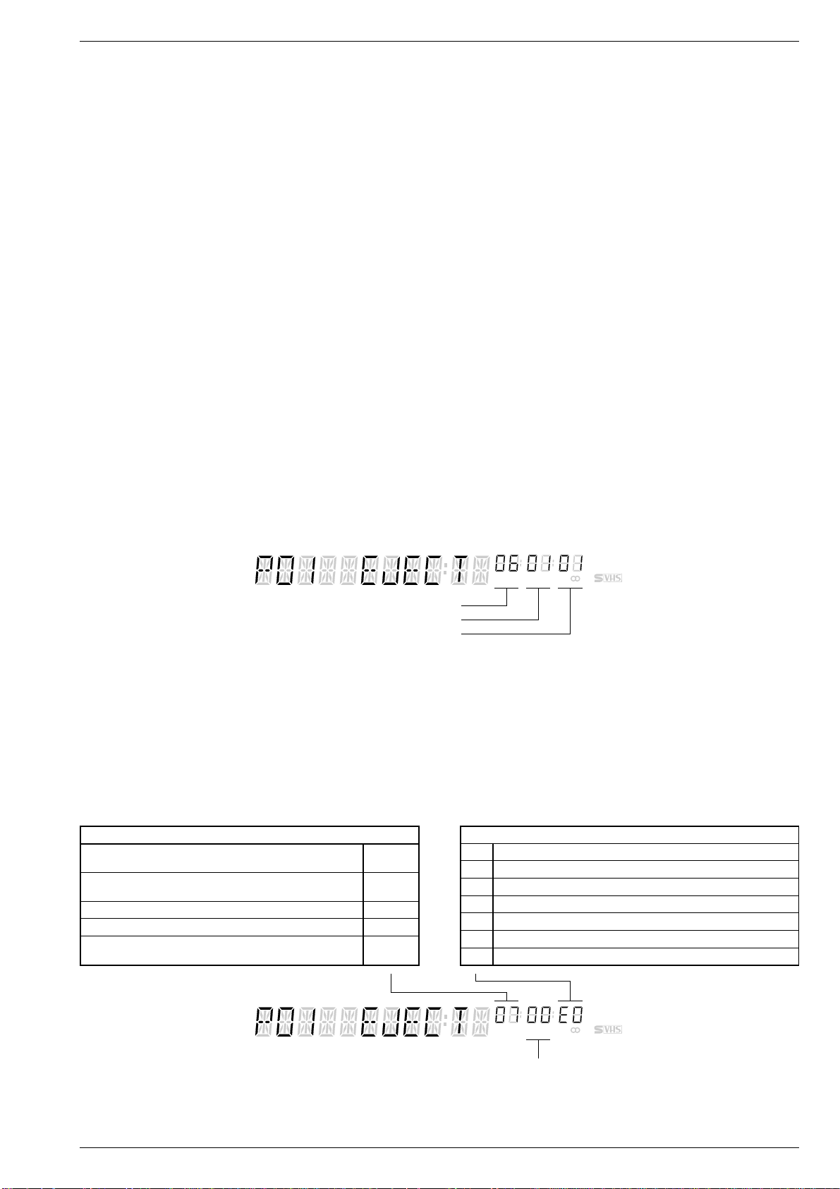
GV 54…, GV 56 …, SE 5106… Allgemeiner Teil / General
Servicetestprogramm und Sonderfunktionen
1. Servicefunktionen
Aufruf, Ebenenkontrolle und Beenden des Servicetestprogrammes
Der Aufruf des Servicetestprogrammes ist bei allen Laufwerksfunktionen
möglich, jedoch nicht während der Einstellfunktionen (z.B. Sendersuchlauf). Während des Servicemodes bleibt das Gerät bei allen
Laufwerksfunktionen voll einsatzbereit.
• Aufruf des Servicetestprogrammes:
Mit dem Fernbediengeber folgendes ausführen:
– Taste "CODE" sooft drücken bis im Display
erscheint
– Zahlenfolge 4 9 3 4 eingeben und mit G bestätigen
– Auf dem Display des Videorecorders erscheinen anschließend
die Werte der ersten Ebene (siehe Pkt. 1.1).
• Ebenenkontrolle der Displayanzeige
Das Servicetestprogramm besteht aus drei Ebenen:
Ebene 1 – Softwarestände
Ebene 2 – Laufwerkstellungen und Fehlercodes / Fehlerstatus
Ebene 3 – Laufwerksensoren und Betriebsstundenzähler
Von einer Ebene zur anderen gelangt man durch Drücken der Taste
"
TIMER ON/OFF
• Beenden des Servicetestprogrammes:
Taste A drücken oder Gerät vom Netz trennen.
" am Gerät. Nach der Ebene 3 folgt wieder die Ebene 1.
"
CODE -- -- -- --
1.1 Ebene 1 des Servicetestprogrammes
Softwarestände
Die 6-stellige 7-Segmentanzeige des Displays ist in 3 x 2-stellige
Zahlenblöcke unterteilt. Von links gelesen sind diese die Softwarestände des EPROMs, des Laufwerksrechners und des Bedienrechners.
Service Test Programme and Special Functions
1. Service Functions
Calling up, Checking the Levels of and Terminating the Service
Test Programme
The service test programme can be called from any tape drive function other
than the data entry functions (e.g. station search). While it is operating in the
service mode, the VCR remains fully operational in all tape drive functions.
• Calling up the Service Test Programme:
"
On the remote control handset:
– Press the "CODE" button repeatedly until
indicated on the display.
– Enter the numbers 4 9 3 4 successively and confirm with G
– The display of the video recorder will then show the values of the
first level (see para 1.1).
Checking the Levels of the Display Indication
The service test programme is subdivided into three levels:
Level 1 – Software versions
Level 2 – Tape deck positions and error codes / error status
Level 3 – Tape deck sensors and operating hours meter
The levels can be changed step by step by pressing the "
ON/OFF
" button on the recorder. Level 3 is again followed by Level 1.
• Terminating the Service Test Programme:
Press the A button or disconnect the video recorder from the mains.
"CODE -- -- -- --
"
is
TIMER
1.1 Level 1 of the Service Test Programme
Software Versions
The 6-place 7-segment display is subdivided into three 2-place blocks
of figures. Reading from left to right these blocks indicate the following
software versions: EPROM, tape deck µC, and keyboard control µC.
Laufwerksrechner / Tape Deck µC (IC7100)
Bedienrechner / Keyboard Control µC (IC7120)
EPROM (IC7250)
1.2 Ebene 2 des Servicetestprogrammes
Laufwerkstellungen und Fehlercodes / Fehlerstatus
Die Laufwerkstellung gibt die Position an, in der sich der Cassettenschacht und die Fädelschlitten befinden.
Der zuletzt aufgetretene Fehlerstatus und Fehlercode wird im UhrRAM gespeichert und bleibt auch dann erhalten, wenn das Gerät vom
Netz getrennt wird. Löschen kann man diesen im Servicemode beim
Aufrufen der Ebene 2 des Servicetestprogrammes durch längeres
Drücken (mindestens 5s.) der Taste "
Laufwerkstellung / Tape Deck Positions
Auswurf / Eject 0A
Index, Vorlauf, Rücklauf / Index, wind, rewind 5C…5F
Ausgefädelt-Stop / Stop threaded out 63…69
Wiedergabeposition / Play position d0…d6
Wiedergabe rückwärts / Play reverse F0
TIMER ON/OFF
" am Gerät.
04…09
60…62
EA…EF
VPSPDC
MAN
STOP TIMER 1 2
LP
1.2 Level 2 of the Service Test Programme
Tape Deck Positions and Error Codes / Error Status
The tape drive position indicates the position of the cassette compartment and of the threading roller units.
The last error status and error code that occurred is stored in the Timer
RAM and is saved even if the VCR is disconnected from the mains. The
data in the memory can be cleared in the service mode when calling
up Level 2 of the Service Test Programme by pressing the "
ON/OFF
" button on the VCR for at least 5 seconds.
Laufwerk Fehlercode / Drive Mechanism Error Code
E0 Kein Fehler / No error
E1 Fädelfehler / Threading error
E2 Kein Capstantacho / No capstan tacho
E3 Band gerissen / Tape torn
E4 Fehlender Wickeltacho links / Missing left reel tacho
E5 Fehlender Wickeltacho rechts / Missing right reel tacho
E6 Kopfscheibenmotorfehler / Headwheel motor error
TIMER
VPSPDC
LP
STOP TIMER 1 2
Laufwerk Fehlerstatus / Tape Deck Error Status
(siehe folgende Seite / see next page)
GRUNDIG Service 1 - 27
MAN
Page 26
Allgemeiner Teil / General GV 54…, GV 56 …, SE 5106…
Laufwerk Fehlerstatus / Tape Deck Error Status
00 Bereitschaft - kein Fehler / Standby - no error
0C Bereitschaft / Standby
1F Wiedergabe rückwärts (3-fach) / Play reverse (3x)
22 Wiedergabe rückwärts (langsam) / Play reverse (slow)
28 Wiedergabe vorwärts (langsam) / Play forward (slow)
29 Standbild / Still
2A Bildsuchlauf vorwärts (2-fach) / Picture search forward (2x)
2C Bildsuchlauf rückwärts (9-fach) / Picture search reverse (9x)
2d Cassettenausgabe / Eject
2E Bildsuchlauf vorwärts (9-fach) / Picture search forward (9x)
2F Wiedergabe rückwärts / Play reverse
30 Pause / Pause
32 Rücklauf / Rewind
34 Vorlauf / Wind
35 Wiedergabe / Play
36 Stop
79 Insert-Schnitt / Insert edit
84 Kopfreinigung / Head cleaning
A8 Einzelbildfortschaltung vorwärts / Frame forward
A9 Einzelbildfortschaltung rückwärts / Frame reverse
AA Bildsuchlauf rückwärts (11-fach) / Picture search reverse (11x)
Ab Bildsuchlauf rückwärts (7-fach) / Picture search reverse (7x)
AC Bildsuchlauf rückwärts (5-fach) / Picture search reverse (5x)
Ad Bildsuchlauf vorwärts (5-fach) / Picture search forward (5x)
AE Bildsuchlauf vorwärts (7-fach) / Picture search forward (7x)
AF Bildsuchlauf vorwärts (11-fach) / Picture search forward (11x)
C5 Bereitschaft-Schacht oben / Standby Eject
C7 Nachvertonen / Audio Dubbing
C8 HiFi-Aufnahme / HiFi Record
C9 Paralleltonaufnahme / Simulcast Record
CA Nachvertonen - Pause / Audio Dubbing Pause
EE Aufnahme - Pause / Record - Pause
37 Aufnahme / Record
Überwachung der Laufwerksfunktionen
Für die Überwachung der Laufwerksfunktionen sind am Laufwerk
Sensoren angebracht. Diese liefern entsprechend der Gerätefunktion
folgende Tachosignale
– WTL / WTR – Wickelteller links / rechts
– FTA – Fädeltacho
– FG – Capstanmotor
– PG/FG – Kopfscheibenmotor.
Fehlt bei der Ansteuerung des Laufwerks ein Tachosignal, dann
versucht das Gerät, den Cassettenschacht in die Stellung "EJECT" zu
bringen.
1.3 Ebene 3 des Servicetestprogrammes
Laufwerksensoren und Betriebsstundenzähler
Die Anzeige zur Kontrolle der Laufwerksensoren erfolgt mit zwei
Digitalstellen. In diesen werden mehrere Sensoren angezeigt. Mit jeder
Betätigung der Sensoren ändert sich der Wert der Anzeige.
Der Betriebsstundenzähler gibt an, wieviele Stunden die Kopfscheibe
rotierte. Hier ist zum Beispiel, die Kopfscheibe 1980 Stunden lang
gelaufen.
Monitoring the Tape Deck Functions
For monitoring the tape deck functions the tape deck is fitted with
sensors which supply the following tacho signals according to the
functions:
– WTL / WTR – reel left / right
– FTA – threading tacho
– FG – capstan motor
– PG/FG – headwheel motor
When one tacho pulse is missing during the operation of the tape deck,
the VCR tries to move the cassette compartment to the "EJECT"
position.
1.3 Level 3 of the Service Test Programme
Tape Deck Sensors and Operating Hours Meter
The tape deck sensors can be checked by a digital two-place indication. These digital places indicate several sensors. The indicated value
changes with each operation of a sensor.
The operating hours meter indicates the number of hours the headwheel has been rotating. In the example below an operating time of
1980 hours is indicated.
Betriebsstundenzähler / Operating hours indicationLaufwerksensoren / Tape deck sensors
VPSPDC
MAN
STOP TIMER 1 2
LP
Wickeltacho rechts / Right reel tacho
Wickeltacho links / Left reel tacho
Init Schalter / Init switch
Bandende / End of tape (TAE)
Bandanfang / Beginning of tape (TAS)
Aufnahmesperre / Record protection
Fädeltacho / Threading tacho (FTA)
Laufwerkstellung und Funktion des Init-Schalters
Das Diagramm zeigt die Funktion des Init-Schalters in Abhängigkeit der
Stellung des Laufwerks. Dafür ist die Anzahl der Fädeltachoimpulse
(FTA) wichtig. Diese Impulse erzeugt der Fädeltachogeber (Flügelrad),
der mechanisch mit dem Fädelmotor verbunden ist.
Tape Deck Position and Function of the Init Switch
The diagram shows the function of the Init switch dependent on the
tape deck position. For this, the number of the threading tacho pulses
(FTA) is important. These signals are generated by the threading tacho
generator (butterfly sensor) which is mechanically connected with the
threading motor.
A: AC, 2V/Div, 0,5s/Div
B: AC, 2V/Div, 0,5s/Div
Cassette eingeschoben / Cassette in
Cassette unten / Cassette down Index, Umsspulen / Index, wind-rewind
1 - 28 GRUNDIG Service
A
B
Init Schalter / Init switch
Fädeltacho-Impuls (FTA)
Threading pulse (FTA)
Wiedergabe / Play
Einfädeln / Thread in
Page 27
GV 54…, GV 56 …, SE 5106… Allgemeiner Teil / General
1.4 Löschen des EEPROMs
Achtung:
Mit dieser Funktion wird das EEPROM gelöscht und initialisiert. Der
kundenspezifische Senderspeicher und das interne Prozessor-RAM
werden ebenfalls gelöscht (ausgenommen Laufwerkparameter).
Zusätzlich werden folgende Kanäle auf den Programmplätzen für
Servicezwecke geladen:
Programm 1 – Kanal 12 PAL Programm 8 – Kanal 44 PAL
Programm 2 – Kanal 21 PAL Programm 9 – frei
Programm 3 – Kanal 68 PAL Programm 10 – Kanal 21 SECAM
Programm 4 – Kanal 08 PAL Programm 11 – Kanal 04 SECAM
Programm 5 – Kanal 60 PAL Programm 12 – Kanal 05 SECAM
Programm 6 – Kanal 02 PAL Programm 13 – Kanal 10 SECAM
Programm 7 – SAT-Programm 7 Programm 14 –Kanal 10 SECAM
Aufruf der RAM- und EEPROM-Löschfunktion
– Auf der Fernbedienung Taste "CODE" drücken
– Zahlenfolge 4 9 3 7 eingeben
– Taste G drücken.
Hinweis:
Nach dem Löschen bzw. dem Tausch des EEPROMs muß das Gerät
neu abgeglichen werden (siehe Abgleich, Kap. 3).
1.5 Löschen der kundenspezifischen Daten
Achtung:
Mit dieser Funktion werden alle kundenspezifische Daten (Uhrzeit,
Sendertabelle, Timer-Daten, …) gelöscht. Die gerätespezifischen
Daten bleiben erhalten.
Aufruf der Löschfunktion
Während dem Anschließen des Gerätes an das Netz eine Gerätetaste
mindestens 5s drücken.
1.4 Erasing the EEPROM
Attention:
This function erases and initializes the EEPROM. The customised
station memory and the internal processor RAM are also erased (with
the exception of tape deck parameters).
Additionally, the following channels are loaded into the programme
positions for servicing purposes:
Programme 1 – channel 12 PAL Programme 8 – channel 44 PAL
Programme 2 – channel 21 PAL Programme 9 – free
Programme 3 – channel 68 PAL Programme 10 – channel 21 SECAM
Programme 4 – channel 08 PAL Programme 11 – channel 04 SECAM
Programme 5 – channel 60 PAL Programme 12 – channel 05 SECAM
Programme 6 – channel 02 PAL Programme 13 – channel 10 SECAM
Programme 7 – SAT programme 7 Programme 14 – channel 69 SECAM
Calling up the RAM and EEPROM Erase Function
– Press the "CODE" button on the remote control
– Enter the numbers 4 9 3 7 sequentially
– Press the G button.
Note:
After the EEPROM has been cleared or replaced the video recorder
must be realigned (see Adjustment, chapter 3).
1.5 Erasing the Customised Data
Warning:
This function erases all customised data (clock time, station table,
timer data, …). The specific data of the machine is not affected by this
function.
Calling up the Erase Function
Press any button on the video recorder for 5s at least while connecting
it to the mains.
1.6 Dauerlaufprüfung
Die Dauerlaufprüfung ist im Servicetestprogramm integriert. Diese hilft
Fehler zu finden, die sporadisch auftreten. Ein erkannter Fehler wird
im EEPROM gespeichert und bleibt erhalten, auch wenn das Gerät
vom Netz getrennt wird.
Aufruf der Dauerlaufprüfung
– Cassette einschieben.
– Dauerlaufprüfung im Servicetestprogramm starten mit einer der
Tasten K, T oder durch Linksdrehen des Shuttle (Rückspulen).
Anschließend durchläuft das Gerät die Dauerlaufprüfung entsprechend dem folgenden Schema.
Beenden der Dauerlaufprüfung
– Auf der Fernbedienung Taste A drücken oder Gerät vom Netz
trennen.
Wiedergabe
Play
T
Bandanfang
Beginning of
tape
1.6 Continuous Operation Test
The continuous operation test is part of the service test programme and
is used to find out occasionally occurring faults. The fault is stored in
the EEPROM and is saved even if the VCR is disconnected from the
mains.
Calling up the Continuous Operation Test
– Insert a cassette.
– Start the continuous operation test in the service test programme by
pressing one of the buttons K, T or by turning the Shuttle counterclockwise (rewind).
The video recorder is then subjected to the continuous operation test
as shown in the diagram below.
Terminating the Continuous Operation Test
– Press the A button on the remote control or disconnect the video
recorder from the mains.
Bandende
End of Tape
Rückspulen
Rewind
Aufnahme
Record
K
GRUNDIG Service 1 - 29
Page 28
Allgemeiner Teil / General GV 54…, GV 56 …, SE 5106…
2. Sonderfunktionen
Aufrufen der Sonderfunktionen
– Auf dem Fernbediengeber die Taste "CODE" drücken
– Codenummer eingeben
– Taste G drücken.
Löschen der Dauerlauffunktionen
– Taste A drücken, Sonderfunktion wird abgebrochen.
Code- Funktion
Nummer
8501 Dauerlauffunktion "Wiedergabe" bis zum
Bandzählerstand beim Dauerlaufbeginn.
Dauerlauf starten mit der Taste T.
8501 Dauerlauf "Aufnahme"
Programmplatz wählen, Sonderfunktion
aufrufen und Taste K drücken.
(city line / super elite)
8510 V-Impuls-Eintastung "AUS"
8511 V-Impuls-Eintastung "EIN"
8513 Durchschleifbetrieb (AV2 nach AV1) aktiviert
8514 Kein Durchschleifbetrieb (AV2 nach AV1)
8516 Bedienebene "VIDEO 1"
8517 Bedienebene "VIDEO 2"
8518 Modulator "AUS"
8519 Modulator "EIN"
8526 10- und 16 Bit-Geberbefehle werden
angenommen
8527 16 Bit-Geberbefehle werden angenommen
8546 Teletext ohne Zeilensprung "312 / 312" (für
Fernsehgeräte mit 50Hz-Bildwechselfrequenz)
8547 Teletext mit Zeilensprung "312 / 313" (für
Fernsehgeräte mit 100Hz-Bildwechselfrequenz)
8560 NICAM-Testton "EIN"
8561 NICAM-Testton "AUS"
8562 Piezo "AUS"
8563 Piezo "EIN"
Display
zeigt
C-PLAY
C-REC
OFF
ON
ON
OFF
ON
OFF
OFF
ON
–
–
OFF
ON
ON
OFF
OFF
ON
2. Special Functions
Calling up the Special Functions
– Press the "CODE" button on the remote control
– Feed in the code number
– Press the G button.
Erasing the Continuous Operation Test Functions
– Press button A to stop the special function.
Code Function
Number
8501 Continuous "Playback" up to the tape counter
reading at the start of the test. Start the test
with button T.
8501 Continuous "Record"
Select a programme position, calling up the
special functions and press the button K.
(city line / super elite)
8510 V-pulse insertion "OFF"
8511 V-pulse insertion "ON"
8513 Loop through (AV2 to AV1) enabled
8514 No loop through (AV2 to AV1)
8516 Remote control address "VIDEO 1"
8517 Remote control address "VIDEO 2"
8518 Modulator "OFF"
8519 Modulator "ON"
8526 10 and 16 bit remote control commands are
accepted
8527 16bit remote control commands are accepted
8546 No line interlacing "312 / 312" for teletext
(eg. for CTV models with 50Hz frame frequency)
8547 With line interlacing "312 / 313" for teletext
(eg. for CTV models with 100Hz frame frequency)
8560 NICAM Test sound "ON"
8561 NICAM Test sound "OFF"
8562 Piezo "OFF"
8563 Piezo "ON"
Display
show
C-PLAY
C-REC
OFF
ON
ON
OFF
ON
OFF
OFF
ON
–
–
OFF
ON
ON
OFF
OFF
ON
8528 N Data-Programmer
(nur über Videoebene 2 möglich)
Aktivieren des Zahlenschlosses
– Auf der Fernbedienung Taste h drücken.
– Mit den Tasten C D der Fernbedienung die Kindersicherung
anwählen und mit G bestätigen.
– "4-stellige Geheimzahl" eingeben und Taste G drücken.
Zahlenschloß entriegeln
– Auf der Fernbedienung Taste h drücken.
– "4-stellige Geheimzahl" eingeben und Taste G drücken.
Entriegeln bei unbekanntem Zahlencode
– Auf der Fernbedienung Taste "CODE" drücken
– Zahlenfolge 4 9 3 4 eingeben
– Taste G und anschließend Taste A drücken, oder Netzstecker
ziehen.
MEMO
8528 N Data Programmer
(only possible via Video 2)
Activating the Security Code
– Press the button h on the remote control.
– With the buttons C D select the programme lock and confirm with
G.
– Enter a "4-place code number" and press G.
Cancelling the Security Code
– Press the button h on the remote control.
– Enter the "4-place code number" and press G.
Cancelling an unknown Number Code
– Press the "CODE" button on the remote control
– Enter the figures 4 9 3 4 sequentially
– Press G followed by button A or pull out the mains plug.
MEMO
1 - 30 GRUNDIG Service
Page 29
GV 54…, GV 56 …, SE 5106… Beschreibungen / Descriptions
Beschreibung
1. Netzteil (OSM / PS)
Typische Daten:
Netzspannung: 220…240V~
Netzfrequenz: 45…65Hz
Maximale Leistung: 40W
Schaltfrequenz: 30…120kHz
Wirkungsgrad: 80% bei maximaler Leistung
Alle Ausgänge sind kurzschlußgeschützt
Sperrwandlerprinzip
Während der Leitphase des Schalttransistors wird Energie vom Netz
in den Trafo übertragen. Diese Energie wird in der Sperrphase an die
Last abgegeben. Mittels der Einschaltzeit und der Frequenz wird die
Energie, die in jedem Zyklus übertragen wird, so geregelt, daß die
Ausgangsspannungen unabhängig von den Änderungen der Last
oder der Eingangsspannung sind. Die Regelung und Ansteuerung des
Leistungstransistors übernimmt IC7010.
Verschiedene Lastfälle
– Leerlauf (STANDBY-Betrieb):
Das Schaltnetzteil arbeitet mit kontrolliert niedriger Frequenz (ca.
50kHz), um die Schaltverluste am Power-MOS-Transistor T7040 zu
minimieren.
– Normalbetrieb (Regelbereich):
Die Schaltfrequenz sinkt mit steigender Last. Das Tastverhältnis
wird hauptsächlich durch die Netzspannung kontrolliert. Die Ausgangsspannungen sind geringfügig lastabhängig.
– Umkehrpunkt:
Bei diesem Punkt der Ausgangscharakteristik ist die übertragene
Leistung am höchsten.
– Überlast:
Das Netzteil arbeitet im Burst-Mode, d.h. die Energie in jedem
Zyklus wird begrenzt, so daß die Ausgangsleistung gering ist.
Schaltungsbeschreibung
Die Netzspannung wird mit dem Brückengleichrichter D6050 gleichgerichtet und mit C2070 gesiebt. Mit L5010 werden Störimpulse des
Netzteils vom Netz ferngehalten. Während der Anlaufphase erfolgt die
Spannungsversorgung des IC7010 an Pin 1 über R3052, R3050 und
C2036. Nach der Anlaufphase wird die Spannungsversorgung über
die Trafowicklung 7 / 3 und D6036 übernommen. Die Induktivität der
Primärwicklung 1 / 6 bestimmt die Eigenfrequenz des Schaltnetzteils
im Normalbetrieb. Die maximale Frequenz wird mit C2012 an
IC7010-(10) vorgegeben.
Während der Einschaltzeit des Schalttransistors T7040 fließt der Strom der gleichgerichteten Netzspannung über die Primärwicklung des Trafos (Kontakte 1 / 6), T7040
und R3048, R3046 nach Masse (primärseitig).
Da die Spannung am Kontakt 1 des Trafos
annähernd konstant ist, steigt der Strom linear.
Seine Stärke ist abhängig von der Netzspannung und der Induktivität der Primärwicklung. Im Trafo bildet sich ein magnetisches Feld, welches einer bestimmten Energiemenge entspricht. Die Sekundärspannungen
sind in dieser Phase so gepolt, daß die Dioden
sperren. Über die Widerstände R3048, R3046,
R3026 wird dem IC7010 an Pin 7 eine
Spannungsabbildung des Primärstroms zugeführt. Übersteigt diese Spannung einen
bestimmten Wert, der abhängig ist von der
Regelspannung an IC7010-(14), wird der
Schalttransistor T7040 abgeschaltet. Dieser
Vorgang wiederholt sich bei jedem Einschalten des Schalttransistors T7040.
Nach dem Abschalten des Schalttransistors
T7040 wird keine Energie in den Trafo übertragen. Die im Trafo gespeicherte Energie baut
sich nun über die Sekundärwicklungen ab (U = – L*∆I/∆t). Durch die
Umkehrung der Polarität der Spannungen am Trafo fließt ein Strom
durch die Sekundärwicklungen des Trafos, durch die Dioden, Elkos
und die Last.
+U
IC7010-(8)
-U
U
GS
IC7010-(3)
T7040
UDS
T7040
ID
Description
1. Power Supply (OSM / PS)
Typical Data:
Mains voltage: 220…240V~
Mains frequency: 45…65Hz
Maximum power: 40W
Switching frequency: 30…120kHz
Efficiency: 80% at maximum load
Short-circuit protection provided for all outputs
Principle of the Blocking-Oscillator Type Transformer
During the conducting phase of the switching transistor energy is
transferred from the mains to the transformer. This energy is fed out to
the load during the phase the transistor is switched off. By means of the
switch-on period and the frequency the energy transfer during each
cycle is so controlled that the output voltages are independent of
changes in the load or the input voltage. Controlling and driving the
power transistor is effected by IC7010.
The Different Load Conditions
– No-load operation (STANDBY):
The switched mode power supply operates at a controlled low
frequency (approx. 50kHz) to minimize the switching losses at the
Power-MOS transistor T7040.
– Normal operation (control range):
The switching frequency decreases along with the increasing load.
The duty cycle is mainly controlled by the mains voltage. The output
voltages are influenced by the load to a minor extent.
– Reversal point:
At this point of the output characteristic the maximum power is
transferred.
– Overload:
The power supply operates in Burst Mode (polling operation mode),
i.e. the energy of each cycle is limited so that the output power is low.
Circuit Description
The mains voltage is rectified by the bridge rectifier D6050 and filtered
by C2070. L5010 is provided to protect the power supply against
interfering pulses from the mains. During the starting phase the power
for IC7010 is supplied to Pin 1 via R3052, R3050 and C2036. After the
starting phase the power is obtained from the transformer winding 7 / 3
and D6036. The inductance of the primary windings 1 / 6 determines
the natural frequency of the switched mode power supply in normal
operating mode. The maximum frequency is determined by C2012 at
I
Dmax
Point of Reversal
ondary windings (U = – L*∆I/∆t). Due to the fact that the polarities of
the voltages are reversed by the transformer current flows through the
secondary windings of the transformer, through the diodes, electrolytic
capacitors into the load.
IC7010-(10).
During the switch-on period of the switching
transistor T7040 the current of the rectified
mains voltage flows through the primary winding of the transformer (contacts 1 / 6), T7040
t
and R3048, R3046 to ground (in the primary
side). Since the voltage at contact 1 of the
transformer is almost constant the current rises
linearly. The intensity of this current depends on
the mains voltage and the inductance of the
primary winding. In the transformer, a magnetic
field develops which corresponds to a certain
t
amount of energy. During this phase, the diodes
are cut off due to the polarity of the secondary
voltages. Via the resistors R3048, R3046, R3026
a voltage which represents the primary current
is fed to Pin 7 of IC7010. If this voltage exceeds
a certain level depending on the control voltage
t
at IC7010-(14), the switching transistor T7040
is switched off. This process is repeated whenever the switching transistor T7040 is switched
on.
As soon as the switching transistor T7040 is
switched off the energy transfer to the trans-
t
former is stopped. The energy accumulated in
the transformer is now transferred to the sec-
GRUNDIG Service 2 - 1
Page 30
Beschreibungen / Descriptions GV 54…, GV 56 …, SE 5106…
Ist die gesamte im Trafo gespeicherte Energie an die Last abgegeben
und das magnetische Feld abgeklungen, so fallen die Spannungen an
den Sekundärwicklungen unter 0V. Diese Nulldurchgänge erkennt
IC7010 an Pin 8. Der Schalttransistor T7040 wird erneut durchgeschaltet und ein neuer Zyklus beginnt.
Die Regelung des Schaltnetzteiles erfolgt durch Verändern der Leitphase des Schalttransistors, so daß entweder mehr oder weniger
Energie vom Netz in den Trafo übertragen wird. Die Regelinformation
kommt vom IC7074, welches die Ausgangsspannung des Schaltnetzteiles überwacht. Der IC7074 ist ein Referenzelement mit einer internen 2,5V-Referenzspannung und einem Vergleichskreis. Diese Regelinformation gelangt über den Optokoppler OK7070 (galvanische Trennung) zum Pin 14 des IC7010. Der IC7010 vergleicht diese Spannung
mit einer internen Referenz. Dieser Vergleich verändert den Pegel, mit
dem die Spannung an Pin 7 des IC7010 (Primärstromabbildung)
verglichen wird.
In der Sperrphase des T7040 begrenzen C2042, R3042, R3044,
D6042 und L5042 die Spannungsspitzen auf der Primärseite.
Zur Vermeidung statischer Aufladungen besitzt das Gate des Schalttransistors T7040 den Pull Down-Widerstand R3040. Die Spannung
am Pin 5 des IC7010 wird zur Rückwärtsregelung (FOLD BACK)
benötigt.
Die maximal entnehmbare Sekundärleistung bestimmen R3048 /
R3046. Das Netzteil geht ab 1V (typisch) an IC7010-(7) in den
Umkehrpunkt.
Die Beschaltung an Pin 11 ist eine Option des IC7010. Mittels C2014
wird die Anlaufphase mit verkürzten Impulsen durchgeführt, so daß die
Schaltfrequenz außerhalb des hörbaren Bereiches liegt.
Auf der Sekundärseite stehen fünf Spannungen (-28V, +33V, +14V,
+8V und +5V) zur Verfügung, die mit den zugehörigen Bauteilen
(Dioden / Kondensatoren / Drosseln) gleichgerichtet und gesiebt sind.
Mit dem zusätzlichen Trafo 5082 wird von der +14V-Spannung die
Heizspannung für das Display abgeleitet. Dieser Transformator wird
vom Bedienrechner über T7558 (Chassisplatte) und T7080 angesteuert bzw. im Stromsparbetrieb abgeschaltet.
Anlaufphase
Nach dem Anschließen des Gerätes ans
Netz steigen ab dem Zeitpunkt t0 folgende
Spannungen an den Pins des IC7010 (siehe Abb.):
– Die Spannung Vcc, IC7010-(1), steigt
entsprechend der Halbwellenladung
Vcc prot
Vcc start
Vdis1
Vdis2
IC7010-(1)
No-Take Over
V
cc
Start-Up
Re-Start
über R3050 / R3052 bis der Spannungswert Vcc Start erreicht ist. Die typische
Stromaufnahme (Icc) ist dabei 0,3mA.
Vref
Die interne Referenzspannung Vref des
IC7010 wird beim Erreichen von Vcc Start
eingeschaltet und die Stromaufnahme
steigt bis 17mA.
– Die Spannung an Pin 11 des IC7010
IC7010 int.
UVL01
nimmt linear bis 2,4V zu. Der IC7010
steuert während dieser Zeit den PowerMOS-Transistors T7040 mit verkürzten
Impulsen an.
– Fällt die Spannung Vcc, IC7010-(1), un-
IC7010 int.
Vpin11
ter den Grenzwert Vdis2 bevor der Umkehrpunkt erreicht wurde, wird der Anlauf gestoppt. Dazu wird T7040 nicht
IC7010-(11)
mehr angesteuert und der IC7010 schal-
ovp out
tet die interne Uref ab (Icc = 0,3mA). Die
V
Spannung Vcc steigt entsprechend einer
Halbwellenladung über R3050 / R3052.
Ein neuer Anlaufzyklus startet.
Normalbetrieb, Überlast und StandbyBetrieb
IC7010 int.
Output
Nach dem Anlauf arbeitet der IC7010 im
Normalbetrieb (Regelbereich). Die Span-
IC7010-(3)
nung an IC7010-(14) ist 2,5V (typisch).
Steigt die Last sekundärseitig, wird die
Einschaltzeit verlängert. Dadurch erhöht
sich der Spitzenspannungswert an
IC7010-(7) "Drainstromabbildung".
Steigt die Last weiter, d.h. auch die Span-
Icc
17mA
0,3mA
IC7010-(1)
nung an IC7010-(7), beginnt der Überlastverstärker des ICs die Impulsbreite der T7040-Ansteuerspannung an
IC7010-(3) zu reduzieren. Dieser Punkt wird als Umkehrpunkt bezeichnet. Die IC-Versorgungsspannung Vcc verhält sich wie die
Sekundärspannungen. Auch diese wird mit zunehmender Last kleiner.
When the whole amount of energy stored in the transformer has been
transferred to the load and no magnetic field is left in the transformer,
the voltages at the secondary windings fall below 0V. These zero
passages are detected by IC7010 at Pin 8. The transistor T7040 is
switched on again and the next cycle is started.
Control of the switched mode power supply is effected by varying the
conducting phase of the switching transistor to the effect that the energy
transferred from the mains to the transformer is increased or reduced.
The control information is obtained from IC7074 which monitors the
output voltage of the switched mode power supply. IC7074 is used as
a reference element with an internal 2.5V reference voltage and a
comparator stage. This control information is taken via the optocoupler
OK7070 (electrical isolation) to Pin 14 of IC7010. This IC7010 compares
this voltage with an internal reference. By means of this comparison the
level of the voltage used to be compared with the voltage at Pin 7 of
IC7010 (representing the primary current) is changed.
During the period T7040 is switched off, C2042, R3042, R3044, D6042
and L5042 limit the voltage peaks in the primary side.
To avoid static charges the gate of the switching transistor T7040 is
provided with the pull down resistor R3040. The voltage at Pin 5 of
IC7010 is used for stepping down the current and the voltage in shortcircuit conditions (FOLD BACK).
The maximum power possible to be taken from the secondary side is
determined by R3048 / R3046. At 1V (typically) on IC7010-(7) the
power supply unit reaches the reversal point.
The external circuit at Pin 11 is an option of IC7010. By means of
C2014 the pulses in the start-up phase are shorter so that the switching
frequency is outside the audible range.
From the secondary side, five voltages (-28V, +33V, +14V, +8V and
+5V) are available which are rectified and filtered by the respective
components (diodes / capacitors / chokes). The additional transformer
5082 is used to derive the heating voltage for the display from the +14V
voltage. This transformer is driven or cut off on the current-saving
standby mode by the keyboard control computer via T7558 (Family
Board) and T7080.
Loop Failure
>2ms
The Start-up Phase
When connecting the video recorder to the
mains the following voltages at the pins of
Normal Mode
IC7010 start to rise at time t0 (see fig.):
– The voltage Vcc, IC7010-(1), increases
according to the half-wave charge via
R3050 / R3052 until it reaches the volt-
t
age level Vcc Start at the typical current
consumption (Icc) of 0.3mA. The internal
reference voltage Vref of IC7010 is
switched on as soon as Vcc Start is
reached and the current consumption
t
increases to 17mA.
– The voltage at Pin 11 of IC7010 rises
linearly up to 2.4V. During this period,
IC7010 drives the Power-MOS transis-
tor T7040 by shortened pulses.
t
– If the voltage Vcc, IC7010-(1), falls below
the limit value Vdis2 before the reversal
point is reached the start-up is stopped.
For this, the drive to T7040 is stopped
and IC7010 switches off the internal Uref
t
(Icc = 0.3mA). The voltage Vcc increases
according to a half-wave charge via
R3050 / R3052. The next start-up cycle
commences.
Normal Operation, Overload and
t
Standby Operation
As soon as the power supply stage is
working, IC7010 operates in the normal
mode (control range). The voltage at
IC7010-(14) is 2.5V (typically). If the load in
t
the secondary side increases, the switchon period is increased. As a result the peak
voltage value at IC7010-(7) "representation of drain current" increases.
If the load continues to increase, that is also
t
the voltage at IC7010-(7), the overload
amplifier of the IC starts to reduce the pulse
width of the T7040 driving voltage at IC7010-(3). This point is the socalled reversal point. The IC supply voltage Vcc behaves in the same
way as do the secondary voltages. This voltage decreases also along
with the increasing load.
2 - 2 GRUNDIG Service
Page 31

GV 54…, GV 56 …, SE 5106… Beschreibungen / Descriptions
Bei Vcc < Vdis1 wechselt der IC7010 in den Abfragebetrieb (Burst
Mode). Die Kurzschlußleistung ist gering, da das Intervall zwischen
den Halbwellenanläufen groß ist. Bei sinkender Last wird die Impulsbreite reduziert. Die Schaltfrequenz erhöht sich bis zur Oszillatorfrequenz des IC7010, die an Pin 10 mit C2012 festgelegt ist. Sinkt die
Last weiter, schaltet der IC7010 ab einer bestimmten Schwelle der
Spannung an Pin 7 (abhängig von der Beschaltung an den Pins 12 / 16)
die Frequenz auf ca. 50kHz zurück (Standby-Betrieb). Dadurch werden die Schaltverluste am Transistor niedrig gehalten.
Überspannung
Bei einer Betriebsspannung Vcc > 17V an Pin 1 des IC7010 sperrt die
Ausgangsstufe.
Übertemperatur
Der IC7010 besitzt einen Übertemperatursensor, der die Logik bei zu
hohen Chip-Temperaturen (typ. 155oC) blockiert. Nach Rückgang der
Temperatur ist ein erneuter Anlauf möglich nach erneutem Anschließen des Gerätes ans Netz.
2. Chassisplatte (OFBG)
2.1 Chassisplatte – Ablaufsteuerung (CC)
Funktionsübersicht:
Die Steuerung des Videorecorders übernimmt der Hauptrechner
(Central Controller, IC7300), der über diverse Bus-Systeme periphere
Funktionsgruppen kontrolliert. Die Kommunikation mit dem Laufwerksrechner (Deck Controller, IC7100), der das Laufwerk steuert, erfolgt
über die Steckerkontakte 1532-(12) "DATD1" und 1532-(10) "CLKD1",
die Kommunikation mit dem Bedienrechner (Display Controller) über
die I2C-Bus Steckerkontakte 1510-(3/4) und das Bus-Interface (INT)
über Steckerkontakt 1510-(9).
Die Ablaufsteuerung ist in folgende Funktionsgruppen unterteilt:
2.1.1 Hauptrechner mit externem Speicher und Parallel-RAM
2.1.2 Funktions- und Schaltspannungserzeugung
2.1.3 RESET der Laufwerksteuerung (DE) und der Bedieneinheit (DC)
2.1.4 Diverse Bus-Systeme
2.1.5 Analogeingänge des Hauptrechners
2.1.6 VPS-Programmabfrage
2.1.7 Uhr-RAM und EEPROM
2.1.1 Hauptrechner mit externem Speicher und Parallel-RAM
Der Hauptrechner (Central Controller) IC7300 übernimmt die Hauptsteuerung des Gerätes. Die Vielzahl der auftretenden Aufgaben sind
mit dem internen Programmspeicher, 6kByte-ROM, nicht zu bewältigen. Hierfür ist es erforderlich, externe Programmspeicher zu verwenden. Dazu benötigt man ein EPROM (je nach Geräteausführung
256kB…512kB), IC7250, und
einen Adress-LATCH, IC7245,
der den Zugriff auf das EPROM
mit steuert. Der Adressbereich
des Hauptrechners läßt nur eine
64kByte-Adressierung zu. Mit
der Adresserweiterung "Bank
Switching", IC7300-(10) ist die
Adressierung von bis zu
512kByte möglich. Damit auf
das EPROM zugegriffen werden kann, ist an IC7300-(50)
"EA" Massepotential. Am
Port 0 (Pins 37…44) des Hauptrechners ist die "Low Order
Address" und am Port 2
(Pins 45…49, 53…55) die "High
Order Address". Nach dem
XTAL1
XTAL2
ALE
PSEN
WR
AD
A
EA
3
RD
3
0-7
0
8-15
2
Schalten des Adress-LATCH
über IC7300-(51) "ALE" werden über Port 0 Daten eingelesen. Da das interne RAM des
Hauptrechners mit 256Byte für
eine Programmierung in "C"
nicht ausreicht, setzt man ein
externes 8kByte-Static-RAM, IC7255, als Datenspeicher ein. Der
Hauptrechner steuert den Zugriff (Lesen und Schreiben) auf das RAM
über Pin 22 "OE" und Pin 27 "WE" des IC7255, während gleichzeitig
das EPROM IC7250 über Pin 24 "OE" abgeschaltet ist.
3 3 3 3 1
T0, T1
TWO 16-BIT
TIMER/EVENT
COUNTERS
PARALLEL
I/O PORTS
&
EXT BUS
P0 P1 P2 P3 TXD RXD P4 T2 T2EX SCL SDA RST EWN
CPU
SERIAL
UART
PORT
3 3 1 1 1 1
0
ALTERNATE FUNCTION OF PORT 0
1
ALTERNATE FUNCTION OF PORT 1
2
ALTERNATE FUNCTION OF PORT 2
3
ALTERNATE FUNCTION OF PORT 3
7
PROGRAM
MEMORY
6K X 8
RAM
8-BIT
I/O
PORT
With Vcc < Vdis1, the IC7010 changes to the polling operation mode
(Burst Mode). The short-circuiting power is low because the interval
between the half-wave starts is large. The pulse width is reduced along
with the decreasing load. The switching frequency increases to the
oscillator frequency of IC7010 which is determined at Pin 10 by C2012.
If the load continues to decrease, IC7010 switches the frequency back
to approx. 50kHz (standby operation) from a certain threshold of the
voltage at Pin 7 (depending on the external circuit connected to
Pins 12 / 16). As a result, the switching losses at the transistor are low.
Overvoltage
At an operating voltage Vcc > 17V at Pin 1 of IC7010 the output stage
is switched off.
Excess Temperature
IC7010 is fitted with an excess-temperature sensor for blocking the
logic if the permissible chip temperatures are exceeded (typ. 155oC).
After the temperature has fallen a new start-up is possible by reconnecting the video recorder to the mains.
2. Family Board (OFBG)
2.1 Family Board – Sequence Control (CC)
Function Overview:
Control of the video recorder is effected by the central processing unit
(Central Controller IC7300) which controls peripheral function groups
via various bus systems. It communicates with the tape deck computer
(Deck Controller, IC 7100) which drives the tape deck via the plug
contacts 1532-(12) "DATD1" and 1532-(10) "CLKD1", communication
with the keyboard control computer (Display Controller) takes place via
the I2C-bus plug contacts 1510-(3/4) and the bus interface (INT) via
plug contact 1510-(9).
The sequence control consists of the following function groups:
2.1.1 Central processing unit with external memory and parallel RAM
2.1.2 Function and switching voltage generation
2.1.3 RESET of the tape deck control (DE) and the keyboard control
unit (DC)
2.1.4 Various bus systems
2.1.5 Analog inputs of the central processing unit
2.1.6 VPS programme scanning
2.1.7 Clock-RAM and EEPROM
2.1.1 CPU with External Memory and Parallel RAM
The central processing unit (Central Controller) IC7300 has complete
control of the video recorder. The multitude of tasks cannot be
accomplished by the internal 6kByte-ROM programme memory so that
external programme memories are needed. For this an EPROM
ADC0-3
AV
83CL580
DATA
MEMORY
256 X 8
RAM
8-BIT INTERNAL BUS
16-BIT
TIMER/
EVENT
COUNTER
POWER
SUPPLY
PWM0T0 T1 INT0 INT1 INT2…INT8
SS
AV
REFP
PWM ADC
T3
2
I C
WATCH-
INTER-
FACE
DOG
TIMER
V
DD
V
SS
an external 8kByte-Static-RAM, IC7255, is used as data memory. The
central processing unit controls the access (reading and writing) to the
RAM via Pin 22 "OE" and Pin 27 "WE" of IC7255 while the EPROM
IC7250 is switched off at the same time via Pin 24 "OE".
(256kB…512kB depending on
the version of the video recorder), IC7250, is used as well
as an address LATCH, IC7245,
which controls the access to
the EPROM. The address range
STADC
of the CPU allows only 64kByte
1
addressing. With the address
extension "Bank Switching",
IC7300-(10), addressing of up
to 512kBytes is possible. To
permit access to the EPROM,
chassis potential is applied to
IC7300-(50) "EA". Port 0 (Pins
37…44) of the central processing unit is the "Low Order Address" and Port 2 (Pins 45…49,
53…55) is the "High Order Address". When the Address
LATCH is enabled via
IC7300-(51) "ALE" data is read
in via Port 0. Since the internal
256Byte-RAM of the central
processing unit is not sufficient
for being programmed in "C",
GRUNDIG Service 2 - 3
Page 32

Beschreibungen / Descriptions GV 54…, GV 56 …, SE 5106…
2.1.2 Funktions- und Schaltspannungserzeugung
Verschiedene Schaltungsteile benötigen eine stabilisierte 12V-Spannung. Diese wird von der +14VA-Spannung des Netzteils abgeleitet
mit T7210, T7215, IC7225 und T7220 und steht als Dauerspannung
"+12VD" zur Verfügung.
Für die Schaltungsteile, die nur in Betrieb Spannung benötigen ist die
+12V-Spannung über das Schieberegisters IC7240-(5) und T7237,
T7230 und T7235 schaltbar. Diese Funktionsspannung trägt die
Bezeichnung "+12VF". Des weiteren ist auch die "+5V2A"-Spannung
(5,4V) über das Schieberegister IC7240-(4) und T7202 / T7200 schaltbar. Die Bezeichnung der Schaltspannung ist "+5VF" bzw. "+5VFD".
Bei den Funktionen "Spulen" und "Bildsuchlauf" (≥3-fach) wird die
Versorgungsspannung des Capstanmotor-Treibers von +8V auf +14V
umgeschaltet. Dies erfolgt vom Laufwerksrechner IC7100-(3) über
Steckerkontakt 1534-(4) und die Transistoren T7204 / T7205.
2.1.3 RESET der Laufwerksteuerung (DE) und der Bedieneinheit (DC)
Nach dem Einstecken des Netzsteckers erzeugt der IC7080 der
Laufwerksteuerung (DE) zusammen mit dem Kondensator C2079
einen Resetimpuls an Pin 19. Dieser setzt den Hauptrechner IC7300
über den Reset-Eingang Pin 15 zurück. Des weiteren gelangt der
Reset-Impuls über T7260, R3264, C2264 an das Schieberegister
IC7240-(15). Dadurch werden die Ausgänge des Schieberegisters
IC7240 solange im "Disable-Zustand" (Outputs Tristate) gehalten, bis
der Hauptrechner seine Initialisierungsphase beendet hat. Nach dieser Zeitspanne erzeugt der IC7240 einen Resetimpuls an den
Pins 11 / 12 und setzt damit den Laufwerksrechner IC7100 und den
Bedienrechner IC7120 zurück. Der "EDIT"-Rechner IC7080 wird über
den Bedienrechner zurückgesetzt.
2.1.4 Diverse Bus-Systeme
a) I2C-Bus mit Ab- und Umschaltung
Der in der Ablaufsteuerung integrierte "Hardware-I2C-Bus" ist ein
bidirektionaler Zweileiter-Bus (SDA / SCL). Über diesen I2C-Bus (Pin 23
– SDA und Pin 22 – SCL) sind wie in der Abbildung dargestellt die
Schaltungsteile bzw. µC mit
dem Hauptrechner verbunden. Die Bedieneinheit benötigt zusätzlich zur Ereignis-
IC7300
SDA
SCL
steuerung die Leitung "INT",
IC7300-(21).
PWM0
Der IC7265 (Uhr/RAM) und
der IC7270 (EEPROM) werden über die gleiche Adresse
angesprochen. Zur Vermeidung einer Adresskollision ist
der I2C-Bus über die Steuer-
PWM0
leitung
, IC7300-(24)
umschaltbar. Bei einem HIGH
Pegel an IC7300-(24) ist nur
der IC7265 (Uhr/RAM) mit
T7261/T7262
T7266/T7267
T7263/T7264
H
L
L
dem Hauptrechner verbunden und bei einem LOW-Pegel der IC7270 (EEPROM) sowie über andere Bus-Adressen alle
anderen Schaltungsteile und µC, die an diesem angeschlossen sind.
Im energiesparenden Betrieb (LOW POWER MODE) ist nur der
IC7265 (Uhr/RAM) mit dem Hauptrechner verbunden (
PWM0
= HIGH).
b) Serielle Schnittstelle zum Laufwerksrechner IC7100
Über die Leitungen DATA-S IC7300-(29) und CLOCK-S IC7300-(30)
ist der Laufwerksrechner mit dem Hauptrechner verbunden. Diese
serielle Schnittstelle arbeitet bidirektional. Master ist der Hauptrechner
IC7300, der den Takt (Clock) generiert. Es werden alle 1,8ms 1Byte
übertragen. Nach der kompletten 27Byte-Übertragung folgt eine Pause von 6 x 1,8ms. Diese benötigt der Laufwerksrechner zur Synchronisierung. Die gesamte Übertragung dauert somit 33 x 1,8ms = 59,4ms.
c) Serielle Schnittstelle zum "EDIT"-Rechner IC7080
Für den Datenverkehr mit dem "EDIT"-Rechner IC7080 zur Camcordersteuerung sind folgende 4 Leitungen erforderlich:
– EDIT 1, IC7300-(16)
Daten vom Hauptrechner zum "EDIT"-Rechner
– EDIT 2, IC7300-(17)
Daten vom "EDIT"-Rechner zum Hauptrechner
– EC-BUSY, IC7300-(18)
Empfangsbestätigung (Acknowledge) vom "EDIT"-Rechner zum
Hauptrechner
– EC-CLK, IC7300-(34)
Clock vom Camera-Rechner zum Hauptrechner
2.1.2 Function and Switching Voltage Generation
Various circuit sections require a stabilized 12V supply to operate. This
voltage is derived from the +14VA voltage of the power supply unit by
means of T7210, T7215, IC7225 and T7220 and is then available as
"+12VD" unswitched voltage.
For those circuit sections which require the +12V supply only during the
time of operation, this voltage is switchable via the shift register
IC7240-(5) and T7237, T7230 and T7235. This function voltage is
called "+12VF". Additionally, the "+5V2A" supply (5.4V) can be switched
via the shift register IC7240-(4) and T7202 / T7200. The designation of
the switching voltage is "+5VF" or "+5VFD". For carrying out the
functions "wind/rewind" and "picture search" (≥3 times) the supply for
the capstan motor driver is switched over from +8V to +14V. This is
done by the tape deck computer IC7100-(3) via plug contact 1534-(4)
and the transistors T7204 / T7205.
2.1.3 RESET of the Tape Deck (DE) and Keyboard Control Units (DC)
After plugging the recorder into the mains, the IC7080 of the tape deck
control unit (DE) generates a reset pulse at Pin 19 together with the
capacitor C2079. This pulse resets the central processing unit IC7300
via the reset input Pin 15. The reset is then passed through T7260,
R3264, C2264 to the shift register IC7240-(15). As a result, the outputs
of the shift register are in "disabled condition" (Outputs Tristate) until
the initialisation of the central processing unit is finished. After this
period, IC7240 generates a reset pulse at Pins 11 / 12 for resetting the
tape deck computer IC7100 and the keyboard control computer
IC7120. The "EDIT" computer IC7080 is reset via the keyboard control
computer.
2.1.4 The Various Bus Systems
a) I2C Bus with Switching-Off/Over Functions
The "Hardware-I2C-Bus" integrated in the sequence control is a
bidirectional two-lead bus (SDA / SCL). As shown in the figure, this
I2C-bus (Pin 23 – SDA and Pin 22 – SCL) connects the circuit sections
and µC respectively with the central processing unit. The keyboard
control unit needs an addi-
Bedieneinheit / Keyboard Control Unit (IC7120)
IN/OUT (IC7770)
AUDIO (IC7010)
tional "INT" lead, IC7300-(21),
for controlling the events.
The address for communicating with IC7265 (Clock/RAM)
and IC7270 (EEPROM) is the
same. For the prevention of
Uhr / Clock/RAM (IC7265)
address collision, the I2C-bus
can be switched over by
means of the control lead
PWM0
Tuner (1359)
NICAM (IC7000)
VPS/PDC (IC7950)
EEPROM (IC7270)
Empfangseinheit / Frontend (IC7570)
Teletext (IC7060)
, IC7300-(24). If a
HIGH level is present at
IC7300-(24), only IC7265
(Clock/RAM) is connected
with the central processing
unit. If a LOW level is applied
to it, IC7270 (EEPROM) as
well as all other circuit sec-
tions and µC connected to it via other bus addresses are switched to
communicate with the central processing unit.
In Low Power Mode, only IC7265 (Clock/RAM) is connected with the
central processing unit (
PWM0
= HIGH).
b) Serial Interface to the Tape Deck Computer IC7100
The tape deck computer and the central processing unit are connected
via the DATA-S IC7300-(29) and CLOCK-S IC7300-(30) leads. This
serial interface works as a bidirectional link. The central processing unit
IC7300 is the master which produces the clock. Every 1.8ms 1 Byte is
transferred. After all 27 Bytes are completely transferred a pause of
6 x 1.8ms follows needed by the tape deck computer for synchronisation. The whole transfer thus takes 33 x 1.8ms=59.4ms.
c) Serial Interface to the "EDIT" Computer IC7080
The following 4 leads are necessary for data communication with the
"EDIT" computer IC7080 for controlling a camcorder:
– EDIT 1, IC7300-(16)
data from the central processing unit to the "EDIT" computer
– EDIT 2, IC7300-(17)
data from the "EDIT" computer to the central processing unit
– EC-BUSY, IC7300-(18)
Acknowledgement from the "EDIT" computer to the central processing unit
– EC-CLK, IC7300-(34)
Clock from camera computer to the central processing unit
2 - 4 GRUNDIG Service
Page 33

GV 54…, GV 56 …, SE 5106… Beschreibungen / Descriptions
In Verbindung mit dem "EDIT"-Rechner IC7080 ist sowohl eine Schnittsteuerung mit "DC-Synchro-Edit" (Panasonic, JVC) als auch mit "LANCEdit" (Sony) möglich.
Bei Geräten ohne dem "EDIT"-Rechner werden die Leitungen EDIT 1
und EDIT 2 direkt zum Hauptrechner IC7300 geführt, um Synchro-Edit
zu ermöglichen.
d) Serielle Schnittstelle zu OSD
Die OSD-Einheit ist über folgende 3 Leitungen mit dem Hauptrechner
verbunden:
CLOCK, IC7300-(14)
DATA, IC7300-(32)
STROBE, IC7300-(12)
Die Übertragung auf diesem 3-Leiter-Bus beginnt mit einem Wechsel
des STROBE von HIGH nach LOW. Die Datenübernahme erfolgt mit
jeder steigenden Flanke des CLOCK. Die Datenübertragung in das
Display-RAM des OSD-IC7900 ist nur während der LOW-Phase des
STROBE möglich.
e) Serieller Bus zur Port-Erweiterung
Da für die vielen Aufgaben des Hauptrechners die Anzahl der Ausgangsports nicht genügen, ist eine Porterweiterung erforderlich. Dazu benutzt der Hauptrechner IC7300 einen seriellen Bus (Port 4.1 – Daten,
Port 4.0 – CLOCK, Port 4.2 – STROBE). Mit diesem Bus sind folgende
Schieberegister verbunden:
– IC7240 Ablaufsteuerung (CC)
– IC7455, IC7460 Empfangseinheit (FE)
– IC7570, IC7580 Video/Chroma (VS)
Über die Leitungen DATEN (Port 4.1) und CLOCK (Port 4.0) werden
Daten in die Schieberegister mit jeweils seriellem Eingang und parallelen Ausgängen geladen und durch die von der STROBE-Leitung
(Port 4.2) kommenden Übernahmeimpulse auf die Ausgänge der
Schieberegister geschaltet.
f) "Megalogic"
Für die Kommunikation zwischen Fernsehgerät, Videorecorder und
Peripheriegeräten dient ein bidirektionaler Einleiter-Bus, Kontakt 10
der Buchse EURO-AV1. In Verbindung mit der durchschleifbaren AVSchaltspannung an Kontakt 8 der Buchse EURO-AV1 sind folgende
Features möglich:
– Der Videorecorder schaltet das Fernsehgerät ein (One Touch Play).
– Der Videorecorder schaltet das Fernsehgerät ein/aus.
Zusätzlich wird die Texteinblendung des Videorecorders am Bildschirm angezeigt (One Touch VPT).
– Der Videorecorder blendet per OSD die aktuelle Laufwerksfunktion
am Bildschirm ein (Status VCR).
– Übertragen der Sendereinstellungen vom Fernsehgerät zum Video-
recorder oder umgekehrt (Download).
– Der Videorecorder nimmt das aktuelle Programm des Fernsehgerä-
tes auf (What you see is what you record).
– Das Fernsehgerät schaltet den Videorecorder ein und benutzt das
Videosignal des Tuners für die Funktion "Bild im Bild" (Pip +/-, Pip-
Quelle).
Die Datenübernahme vom Kontakt 10 der Buchse EURO-AV1 erfolgt
über den Impulsformer T7710 / T7712 ("IN/OUT"-Schaltungsteil) an
IC7300-(31). Die Datenausgabe an IC7300-(13) gelangt über T7715
("IN/OUT"-Schaltungsteil) zum Kontakt 10 der Buchse EURO-AV1.
g) SAT-Tuner-Steuerung
Der Videorecorder kann bei SAT-Aufnahme einen an der Klinkenbuchse angeschlossenen SAT-Receiver zur vorprogrammierten Zeit
auf ein vorprogrammiertes SAT-Programm schalten. Der Hauptrechner
IC7300 überträgt dazu über Pin 33 die erforderlichen Daten an die
Klinkenbuchse 1920 und schaltet den Videorecorder auf SAT-Aufnahme. Das aufzunehmende FBAS-Signal gelangt über den Steckerkontakt 20 der Buchse EURO-AV1/2 zum "IN/OUT"-Schaltungsteil
(IC7770).
2.1.5 Analogeingänge des IC7300
Die Analogsignale der Empfangseinheit (AGC / AFC) und des AudioSchaltungsteiles (Aussteuerungspegel L / R) gelangen über 4 Analogeingänge AD0…AD3 zum Hauptrechner IC7300-(1…4).
Das AGC-Signal an IC7300-(4) dient zur Auswertung der Empfangsfeldstärke (Sendersortierung nach Feldstärke).
Das AFC-Signal an IC7300-(3) dient zur Feinabstimmung des Tuners
auf die genaue Empfangsfrequenz. Bei optimaler Abstimmung liegen
an diesem Eingang (AD1) 2,5V.
Die Aussteuerungspegel des linken und rechten Audio-Kanals an
IC7300-(1/2) werden ausgewertet, um über den I2C-Bus Daten für die
In connection with the "EDIT" computer IC7080 both editing methods
are possible "DC-Synchro-Edit" (Panasonic, JVC) and "LANC-Edit"
(Sony).
In video recorders which are not fitted with an "EDIT" computer, the
leads EDIT 1 and EDIT 2 are directly routed to the central processing
unit IC7300 in order to allow Synchro Editing.
d) Serial Interface to the On Screen Display
The OSD unit is linked with the central processing unit via the following
3 leads:
CLOCK, IC7300-(14)
DATA, IC7300-(32)
STROBE, IC7300-(12)
Communication on this 3-lead-bus is started by the STROBE changing
from HIGH to LOW. Data transfer is carried out with every leading edge
of the CLOCK. Data transfer to the Display-RAM of the OSD-IC7900
is only possible during the LOW phase of the STROBE.
e) Serial bus for Port Expansion
As the number of output ports is not enough to accomplish the
multitude of tasks carried out by the central processing unit, a port
expansion circuit is necessary. For this, the central processing unit
IC7300 employs a serial bus (port 4.1 - data, port 4.0 - CLOCK,
port 4.2 - STROBE) linking the following shift registers:
– IC7240 sequence control (CC)
– IC7455, IC7460 frontend (FE)
– IC7570, IC7580 Video/Chroma (VS)
Via the DATA (port 4.1) and CLOCK (port 4.0) leads, the data is loaded
into the shift registers each with serial input and parallel outputs and is
then switched to the outputs of the shift registers by means of the
transfer pulses coming in from the STROBE lead.
f) "Megalogic"
Communication between the television receiver, video recorder, and
peripheral units is realized by a bidirectional single-lead bus, contact
10 of the EURO-AV1 socket. In connection with the loop-through AV
switching voltage at contact 8 of the EURO-AV1 socket the following
features are possible:
– The video recorder switches the TV receiver on (One Touch Play).
– The video recorder switches the TV receiver off/on.
Additionally, the text information from the video recorder is indicated
on the screen (One Touch VPT).
– The video recorder displays the current operating mode of the deck
via OSD on the screen (VCR Status).
– Transfer of the programmed television stations from the television
receiver to the video recorder and vice versa (Download).
– The video recorder records the currently viewed programme of the
television receiver (What you see is what you record).
– The television receiver switches the video recorder on and uses the
video signal from the tuner for the "picture in picture" function
(Pip +/-, Pip source).
The data from contact 10 of the EURO-AV1 socket is fed in via the pulse
shaper T7710 / T7712 ("IN/OUT" circuit section) at IC7300-(31). The
data fed out at IC7300-(13) is passed through T7715 ("IN/OUT" circuit
section) to contact 10 of the EURO-AV1 socket.
g) SAT Tuner Control
For recording a SAT programme, the video recorder can switch over
a SAT Receiver connected to the jack socket to a preprogrammed SAT
programme at a preprogrammed time. For this the central processing
unit IC7300 transfers the necessary data via Pin 33 to the jack socket
1920 and switches the video recorder to the SAT recording mode. The
CCVS signal to be recorded is fed through plug contact 20 of the
EURO-AV1/2 socket to the "IN/OUT" circuit section (IC7770).
2.1.5 Analog Inputs of IC7300
The analog signals from the frontend (AGC / AFC) and from the audio
circuit section (control level L / R) are passed through 4 analog inputs
AD0…AD3 to the central processing unit IC7300-(1…4).
The AGC signal at IC7300-(4) is used to evaluate the field strength of
the received signal (sorting of the stations according to their field
strength).
The AFC signal at IC7300-(3) is used for precise tuning in of the
reception frequency. When the tuner is precisely tuned, the voltage
level at this input (AD1) is 2.5V.
The control levels of the left and right audio channels at IC7300-(1/2)
are evaluated to supply data to the automatic level control of audioIC7010 via the I2C-bus. This data is also used to drive the level control
indicator via the keyboard control computer.
Aussteuerungsautomatik des Audio-IC7010 zu liefern. Zusätzlich wird
anhand der Daten die Aussteuerungsanzeige über den Bedienrechner
angesteuert.
GRUNDIG Service 2 - 5
Page 34

Beschreibungen / Descriptions GV 54…, GV 56 …, SE 5106…
2.1.6 VPS-Programmabfrage
Der Hauptrechner schaltet bei mehr als einer vorprogrammierten VPSSendung in einen Abfrage-Modus. Dazu stimmt er in einem bestimmten Zyklus den Tuner kurzzeitig auf die entsprechenden Sender ab.
Der IC7950 (Schaltungsteil VPS/PDC) liest die aktuellen VPS-Daten
aus und überträgt sie über den I2C-Bus zum Hauptrechner. Damit ist
gewährleistet, daß der Hauptrechner auch von den Sendeanstalten
vorgezogene Beiträge erkennt und den Videorecorder entsprechend
steuert.
2.1.7 Uhr-RAM und EEPROM
Der IC7265 erzeugt mit dem 32,768kHz-Quarz den Uhrtakt. Aus
diesem wird im IC7265 Uhrzeit und Datum generiert und über den I2CBus dem Hauptrechner IC7300 zugeführt. Das im IC7265 befindliche
16Byte-RAM wird zur Hälfte von der Uhr benötigt, so daß noch ein
freier Speicherplatz von 8Byte verfügbar ist. Dieser ist belegt mit z.B.
Sync. Zähler, Bandzähler und Flags.
Bei fehlender Versorgungsspannung (Netzausfall, gezogener Netzstecker) gewährleistet eine Lithium-Batterie den Datenerhalt.
Im EEPROM IC7270 (je nach Geräteausführung 8kBit oder 16kBit)
sind folgende Daten/Codes gespeichert: Timer-Daten, Titel, Senderkanäle, Senderkürzel, ShowView-Leitzahlen, Kindersicherungscode,
usw. Die Datenübertragung erfolgt über den I2C-Bus.
2.2 Chassisplatte – Empfangseinheit (FE)
Die Empfangseinheit hat die Aufgabe, das vom Tuner kommende
Signal zu verstärken und zu demodulieren. Es entstehen dabei das
FBAS-Signal sowie die NF-Signale:
– Mono: IC7520-(10)
– Stereo: Links: IC7570-(12); Rechts: IC7570-(11)
– Zweiton: Ton 1: IC7570-(12); Ton 2: IC7570-(11)
Vom Tuner kommt das ZF-Signal an das Oberflächenwellenfilter
F1027. Hier erfolgt die Bild-/Ton-Signaltrennung.
Bildverarbeitung
Über IC7520-(1/2) wird die Bild-ZF eingespeist. Es folgt ein regelbarer
Breitbandverstärker, Synchrondemodulator mit aktiver Trägerregenerierung (PLL), ein Videoverstärker, sowie die Regelspannungserzeugung für den Tuner. Von IC7520-(18) gelangt das
FBAS-Signal über R3536 oder den Ton-Trap F1045 an IC7520-(19).
Über eine Bufferstufe, IC7520-(8) und eine Stufe zur Chromaanhebung (T7610 / T7620) leitet man das FBAS-Signal zum "IN/OUT"Schaltungsteil.
Tonverarbeitung
Das Ton-ZF-Signal gelangt nach der Bild-/Ton-Signaltrennung im
Oberflächenwellenfilter F1027 zum IC7520-(27/28). Anschließend
führt man dieses über einen regelbaren Verstärker zum Umsetzer. In
diesem erfolgt die Umsetzung auf 5,5MHz / 5,742MHz. Das 5,5MHzSignal gelangt von IC7520-(17) über das Filter F1033 zu IC7520-(15).
Das 5,742MHz-Signal wird von IC7520-(20) über das Filter F1040 dem
IC7520-(14) zugeführt. Beide Signale durchlaufen anschließend je
einen Synchrondemodulator mit nachfolgendem Verstärker und gelangen über IC7520-(10/11) zum Stereodecoder, IC7570-(7/8).
Mono-Ton
Bei Monosendungen ist nur an IC7520-(10) ein Signal vorhanden. Die
Auswerteschaltung im Decoder IC7570 erkennt den MONO-Status und
teilt dies über den I2C-Bus (Pins 1 / 20) dem Hauptrechner IC7300 mit.
Von ihm werden über den I2C-Bus die Ausgangswahlschalter im IC7570
auf MONO gesetzt und das Ton-Signal auf die Ausgänge, Pins 12 / 11,
geschaltet. Von hier gelangt es für die FM-Aufzeichnung zum AudioSchaltungsteil. Für die Längsspuraufzeichnung führt man das Tonsignal von IC7520-(10) dem Audio-Schaltungsteil (Standardton) zu.
Stereo-Ton
Bei Stereosendungen steht an IC7520-(10) das Summensignal
und an Pin 11 das R-Signal mit Pilotton (mit 117Hz amplitudenmoduliert). Über den Pilotkreis (C2584 / L5582) und Pin 5 des IC7570 gelangt
das Pilotsignal zur Auswerteschaltung. In dieser Schaltung erkennt der
Decoder anhand des 117Hz-Signals den Stereo-Status und teilt dies
über den I2C-Bus dem Hauptrechner mit. Dieser steuert über den I2CBus die Matrix im IC7570 so, daß aus den Signalen
Stereosignale L und R entstehen und setzt den Ausgangswahlschalter
L + R
2
auf "Stereo". An den Pins 12 (Links) und 11 (Rechts) werden die Signale
ausgekoppelt und dem Audio-Schaltungsteil zugeführt.
L + R
2
und R die
2.1.6 VPS Programme Scanning
The central processing unit takes up a scanning mode if two and more
VPS transmissions have been preprogrammed. For this, the computer
tunes the tuner for a short time at certain intervals to the respective TV
stations. The IC7950 (VPS/PDC circuit stage) reads out the current
VPS data and transfers it on the I2C-bus to the central processing unit.
This is to ensure that the sequence control computer detects also
programmes which are broadcasted at an earlier time than originally
planned, and that the video recorder is controlled accordingly.
2.1.7 Clock RAM and EEPROM
The clock pulse is generated in IC7265 with the 32.768kHz crystal
oscillator. From this pulse, the IC7265 generates the time and date
which are then supplied on the I2C-bus to the central processing unit
IC7300. Half of the storage capacity of the 16Byte-RAM integrated in
IC7265 is used for storing the clock data.The remaining 8Byte storage
capacity is used for example for the sync counter, tape counter and
flags.
A lithium battery ensures that the data is held in the case of an
interruption of the power supply (mains failure, disconnected mains
plug).
The EEPROM IC7270 (8kBit or 16kBit depending on the VCR version)
holds the following data/codes: timer data, titles, station channels,
abbreviated station names, ShowView code numbers, programme
lock etc.. The data is transferred via the I2C-bus.
2.2 Family Board – Frontend (FE)
The frontend has the task of amplifying and demodulating the signal
coming in from the Tuner Module. It produces the CCVS signal and the
following AF signals:
– Mono sound: IC7520-(10)
– Stereo sound: Left: IC7570-(12); Right: IC7570-(11)
– Two channel sound: Sound 1: IC7570-(12); Sound 2: IC7570-(11)
The IF signal from the tuner is fed to the surface wave filter F1027 in
which the video and audio signals are separated from each other.
Video Processing
The video IF is fed in on IC7520-(1/2). The signal passes through a gain
controlled wideband amplifier, a synchronous demodulator with active
carrier regeneration (PLL), a video amplifier and also a gain control
voltage generation stage for the tuner. From IC7520-(18) the CCVS
signal is fed through R3536 or the sound trap F1045 to IC7520-(19).
Via a buffer stage, IC7520-(8) and a stage for lifting the chroma signal
(T7610 / T7620) the CCVS signal is taken to the IN/OUT circuit section.
Sound Processing
The sound-IF signal resulting from video/sound signal separation in
the surface wave filter F1027 is passed to IC7520-(27/28). Subsequently, this signal is taken via a gaincontrolled amplifier to the
converter in which the signal is converted to 5.5MHz / 5.742MHz. The
5.5MHz signal is taken from the IC7520-(17) via the filter F1033 to
IC7520-(15). The 5.742MHz signal from IC7520-(17) passes the filter
F1040 and is applied to IC7520-(14). Each of the two signals then
passes through a synchronous demodulator followed by an amplifier
and, via IC7520-(10/11), are carried to the stereo decoder IC7570-(7/8).
Mono Sound
On Mono broadcasts only a signal is present only at IC7520-(10). The
evaluation circuit in the decoder IC7570 identifies the MONO status
and advises the central processing unit IC7300 via the I2C bus (pins 1 /
20). Via the I2C bus, the central processing unit sets the output
selection switches in IC7570 to MONO and the sound signal is
connected to the output pins 12 / 11. From there, the signal is taken to
the Audio circuit section for FM recording. For longitudinal track
recording, the sound signal is fed from IC7520-(10) to the Audio circuit
section (Standard Sound).
Stereo Sound
On Stereo broadcasts the sum signal
and the R-signal with pilot tone (117Hz amplitude modulated) is
present on pin 11. Via the pilot circuit (C2584 / L5582) and pin 5 of
IC7570 the pilot signal is fed to the evaluation circuit. In this circuit the
decoder identifies the stereo status from the presence of the 117Hz
signal and advises the central processing unit via the I2C bus. The
central unit controls the matrix in IC7570 via the I2C bus so that from
the signals
sets the output selection switch to "Stereo". On pins 12 (L) and 11 (R)
L + R
and R, the Stereo signals L and R are obtained. It also
2
the signals are fed out and applied to the Audio circuit section.
L + R
is present on IC7520-(10)
2
2 - 6 GRUNDIG Service
Page 35

GV 54…, GV 56 …, SE 5106… Beschreibungen / Descriptions
Zweiton
Bei Zweitonsendungen steht an IC7520-(10) Ton 1 und an IC7520-(9)
Ton 2 mit Pilotton (274Hz amplitudenmoduliert). Durch eine Auswerteschaltung erkennt der Decoder anhand des 274Hz-Signals den
Zweiton-Status und teilt dies dem Ablaufrechner über den I2C-Bus mit.
Von diesem werden über den I2C-Bus die beiden Kanäle durch den
Ausgangswahlschalter auf Ton 1 (Pin 12) und Ton 2 (Pin 11) geschaltet und dem Audio-Schaltungsteil zugeführt.
2.3 Chassisplatte – IN/OUT (IO)
Allgemeines
Die universelle Einsatzmöglichkeit der Geräte erfordert eine spezielle
Verteilung der Eingangs- und Ausgangssignale, entsprechend der
Betriebsart. Dazu ist ein Matrix-Schalter-IC (IC7770) nötig. Des weiteren erfolgt mit dem Schalter IC7840 die Umschaltung vom Bild-FBASSignal auf das Teletext-FBAS-Signal.
2.3.1 Aufnahme-, Durchschleif- und Wiedergabe-Betrieb
Die Selektierung und Verteilung der Signale erfolgt im Matrix-Schalter
IC7770. An diesem Matrix-Schalter stehen die Eingangssignale von
den Bezugsquellen (EURO-AV1, EURO-AV2, HF, EE/PB) an. Diese
werden geklemmt, entsprechend der Betriebsart ausgewählt, verstärkt und den Schaltungsteilen für die Bild-Verarbeitung bzw. Ausgangsbuchsen zugeführt. Die Selektierung des Cinch Video-Signales
(CV) von der Bedieneinheit erfolgt über den Pin 17 des IC7770 (aktiv
bei LOW) und der Transistorgruppe T7790 / T7794 / T7796. Dabei ist
der Ausgang des IC7770-(1) inaktiv.
Der Hauptrechner IC7300 steuert den Matrix-Schalter über den I2C-Bus.
2.3.2 Decoder-Betrieb
Aus urheberrechtlichen und finanztechnischen Gründen verschlüsseln einige private Fernsehanstalten die Bild- und Tonsignale. Zum
Entschlüsseln dieser Signale benötigt der Empfänger einen entsprechenden PAY-TV-Decoder.
Technische Ausführung
An der Buchse EURO-AV2 ist der PAY-TV-Decoder und über die
Buchse EURO-AV1 das Fernsehgerät angeschlossen.
Bei dieser Zusammenschaltung der Geräte kann der PAY-TV-Decoder ohne Umstecken vom Fernsehgerät und vom Videorecorder
benutzt werden.
Bei der Benutzung des Videorecorders leitet man die codierten Bildund Audiosignale über die Buchse EURO-AV2 zum PAY-TV-Decoder.
In diesem werden die Signale decodiert und über die Buchse EURO-AV2
dem Videorecorder wieder zugeführt. Dieser Signalweg muß beim
Einstellen der Programme programmbezogen freigegeben sein. Bei
der Benutzung des Fernsehgerätes leitet man die codierten Bild-und
Audiosignale von diesem über die Buchse EURO-AV1 und die Buchse
EURO-AV2 zum PAY-TV-Decoder. In diesem werden die Signale
decodiert und über die Buchsen EURO-AV2 und EURO-AV1 dem
Fernsehgerät wieder zugeführt.
Die Zusammenschaltung der Geräte erfolgt über den Matrixschalter
IC7770 und IC7010 (Audio-Schaltungsteil).
2.3.3 "Follow TV"
Diese Schaltung hat die Funktion, jedes einzelne Fernseh-Programm
im Videorecorder auf den gleichen Programmplatz abzuspeichern wie
im angeschlossenen Fernsehgerät.
Hierfür vergleicht die Schaltung "Follow TV" das FBAS-Signal der
Empfangseinheit des Videorecorders mit dem des Fernsehgerätes.
Das FBAS-Signal von der Empfangseinheit wird zum T7860 geleitet,
der das Signal invertiert und verstärkt. Das FBAS-Signal des Fernsehgerätes gelangt über die Buchse EURO-AV1 und den Matrixschalter
IC7770 zum T7865. Beide Signale werden danach addiert und zum
Pin 2 des Komparators IC7875 geleitet. Der Komparator IC7875
vergleicht die addierten FBAS-Signale mit der Referenzspannung an
Pin 3. Wenn beide FBAS-Signale gleich sind, dann ist die addierte
Spannung an Pin 2 des Komparators größer als die Referenzspannung
an Pin 3. Der Komparator gibt an Pin 1 einen LOW-Pegel aus, der über
das Siebglied R3883 / C2883 dem Hauptrechner IC7300-(19) zugeführt wird. Der Hauptrechner speichert anschließend das empfangene
Programm auf den gleichen vorgegebenen Programmplatz wie das
des Fernsehgerätes.
Two-channel Sound
On two-channel sound broadcasts, the sound channel 1 is present on
IC7520-(10) and the sound channel 2 with pilot tone (274Hz amplitude
modulated) is present on IC7520-(9). By means of the evaluation
circuit the decoder identifies the two-channel status from the 274Hz
signal and advises the central processing unit via the I2C bus. The
central unit controls the output selection switch via the I2C-bus so that
sound channel 1 (pin 12) and sound channel 2 (pin 11) are provided
and connected to the Audio circuit stage.
2.3 Family Board – IN/OUT (IO)
General
The universal applicability of these video recorders requires special
facilities for distributing the input and output signals corresponding to
the operating mode. For this, a matrix switch IC (IC7770) is used. In
addition, the switch IC7840 serves the purpose of switching over from
the video-CCVS-signal to the teletext-CCVS-signal.
2.3.1 Record, EE and Playback Modes
The signals are selected and distributed in the matrix switch IC7770.
This matrix switch is supplied with the input signals from the sources
(EURO-AV1, EURO-AV2, HF, EE/PB). The signals are clamped,
selected according to the operating mode, amplified, and fed to the
circuit sections for video processing and the output sockets, respectively. The Cinch-Video signal (CV) from the keyboard control unit is
selected via pin 17 of IC7770 (active at LOW level) and the transistor
network T7790 / T7794 / T7796. The output of IC7770-(1) is not active
in this case.
The central computer IC7300 controls the matrix switch via the I2C-bus.
2.3.2 Decoder Operation
For financial and copyright reasons, a couple of independent television
stations transmit scrambled video and audio signals so that a Pay-TVDecoder is required to descramble the signals.
Technical Realization
The Pay-TV-Decoder is connected to the EURO-AV2 socket and the
TV receiver to the EURO-AV1 socket.
This connection makes it possible to operate the Pay-TV-Decoder in
combination with the TV receiver and also with the video recorder
without changing the connections.
When using the video recorder, the coded video and audio signals are
taken via the EURO-AV2 socket to the Pay-TV-Decoder. The Decoder
descrambles the signals and feeds them back to the video recorder.
This signal path must be released for the respective programmes when
setting the programmes.
Used with a TV receiver, the coded video and audio signals are fed
from the TV through the EURO-AV1 socket and the EURO-AV2 socket
to the Pay-TV-Decoder where the signals are descrambled and then
returned to the TV receiver via the EURO-AV2 socket and the
EURO-AV1 socket.
The sets are interconnected by the matrix switch IC7770 and IC7010
(Audio circuit stage).
2.3.3 "Follow TV"
The function of this circuit section is to store each individual television
programme in the video recorder on the same programme position as
it is stored in the TV receiver.
For this purpose, "Follow TV" compares the CCVS signal from the
frontend of the video recorder with that of the television receiver. The
CCVS signal from the frontend is passed to T7860 where it is inverted
and amplified. The CCVS signal from the TV receiver is fed through the
EURO-AV1 socket and the matrix switch IC7770 to T7865. Both
signals are then added and taken to Pin 2 of the comparator IC7875.
The comparator IC7875 compares the added CCVS signals with a
reference voltage at Pin 3. When both CCVS signals have the same
level, the added voltage at Pin 2 of the comparator will consequently
be higher than the referenece voltage at Pin 3. The comparator
supplies at Pin 1 a LOW level which is applied via the filter section
R3883 / C2883 to the central processing unit IC7300-(19). The central
processing unit then stores the received programme at the same
predetermined programme position as that of the TV receiver.
GRUNDIG Service 2 - 7
Page 36

Beschreibungen / Descriptions GV 54…, GV 56 …, SE 5106…
2.4 Chassisplatte – Audio (AU)
Der Audio-Schaltungsteil bereitet die Audiosignale auf, für die Schrägspuraufzeichnung (FM-Ton) und für die Längsspuraufzeichnung
(Standardton). Das Kernstück bildet hierfür der IC7010, der über den
I2C-Bus vom Hauptrechner IC7300 gesteuert wird.
2.4.1 Chassisplatte – FM-Ton
Die Stereoton-Kanäle sind symmetrisch aufgebaut. Deswegen ist die
Beschreibung auf den linken Kanal (L) beschränkt.
Funktionsübersicht
Im FM-Ton-Schaltungsteil werden bei Aufnahme die Audio-Signale im
Eingangswahlschalter ausgewählt und komprimiert. Anschließend
werden die 2 Trägerfrequenzen (1,4MHz - linker und 1,8MHz - rechter
Kanal) mit den Audio-Signalen frequenzmoduliert und über die beiden
rotierenden Audioköpfe auf das Band aufgezeichnet.
Bei Wiedergabe wird die vom Band, über die rotierenden Audioköpfe
abgetastete Information dem FM-Ton-Schaltungsteil zugeführt. Nach
der Demodulation expandiert man die Signale wieder auf die ursprüngliche Dynamik (Rauschunterdrückung) und führt diese den Ausgängen (LINE, EURO-AV, Modulator) zu.
Aufnahme
Die Eingangssignale (LINE, EURO-AV1, EURO-AV2 oder HF-Ton)
werden dem IC7010 über die Pins 1…11 zugeführt und im
Eingangswahlschalter selektiert. Das ausgewählte NF-Signal gelangt
vor und nach dem digitalen Pegelsteller über je eine Additionsstufe
zum Eingangswahlschalter des Standardton-Schaltungsteils für die
Längsspuraufzeichnung. Des weiteren führt man das ausgewählte
NF-Signal dem internen Tiefpaßfilter (AUDIO LPF) zu. Von dort
durchläuft es die Kompressionsstufe (Komprimierung um den Faktor 2)
sowie die Rauschunterdrückung (NOISE REDUCTION) und gelangt
über IC7010-(64) / C2112 / IC7010-(63) an die Audio-Begrenzerstufe
(AUDIO CLIPPER) zur Hubbegrenzung. Im FM-Modulator "CCO" wird
das NF-Signal auf 1,4MHz-FM-Signal umgesetzt. Nach dem HFTiefpaß (HF LPF) addiert man dieses mit dem 1,8MHz-FM-Signal des
rechten Kanals. Anschließend verstärkt man das Summenprodukt und
führt es über IC7010-(56) und Steckerkontakt 1507-(8) dem
Kopfverstärker auf der Chassisplatte II (OKV++G) zu.
Beim Aufsprechen der beiden Trägerfrequenzen auf das Band ist die
HF-Amplitude des 1,8MHz-Trägers um ca. 9dB größer, da dieser
Träger vom nachfolgenden Videokopf stärker angelöscht wird. Somit
ist gewährleistet, daß bei Wiedergabe die beiden HF-Träger annähernd die gleiche Amplitude aufweisen.
Wiedergabe
Das Signal vom Band wird dem FM-Ton-Schaltungsteil über 1507-(6)
zugeführt und an IC7010-(57) weitergeleitet. Im IC7010 durchläuft es
die HF-AGC-Stufe und in den integrierten Bandpaß-Filtern trennt man
es für die Signalverarbeitung (1,4MHz-Links / 1,8MHz-Rechts). Anschließend führt man die Signale über die HF-Begrenzer (HF LIMITER)
den Demodulatoren (PLL) zu. Das demodulierte NF-Signal (L) gelangt
anschließend zur Sample & Hold-Schaltung (S & H). Diese dient dazu,
Störungen im NF-Signal, bedingt durch den Kopfwechsel beim Abtasten des Signals, zu unterdrücken. Der hierfür benötigte "Hold
Switch-Impuls" wird im IC7010 mit Hilfe des HI-Ton-Impulses erzeugt.
Dieser gelangt vom Laufwerksrechner IC7100-(20) und Steckerkontakt
1507-(2) zum IC7010-(61). Das NF-Signal (L) leitet man über
IC7010-(63) / C2112 / IC7010-(64), den Tiefpaßfilter (AUDIO LPF)
und die Rauschunterdrückung (NOISE REDUCTION) zu den Ausgangswahlschaltern. Diesen wird intern auch das Standardton-Signal
der Längsspur zugeführt. Die ausgewählten Signale werden in der
Additions-Stufe addiert und über IC7010-(18) zum Modulator weitergeleitet. Das ausgewählte Ausgangsignal (L) führt man über einen
Ausgangstreiber und IC7010-(21) den Ausgängen (LINE / EURO-AV1)
und über IC7010-(19) dem Ausgang (EURO-AV2) zu. Vom Ausgangswahlschalter für den Kopfhörer leitet man das NF-Signal über einen
Pegelsteller und IC7010-(25) zur Kopfhörerbuchse. Des weiteren
gelangt das NF-Signal über den NF-Hüllkurvengleichrichter und
IC7010-(23) zum Hauptrechner, IC7300-(2). Dieser steuert über die
serielle Schnittstelle und den Bedienteilrechner die Aussteuerungsanzeige auf der Bedieneinheit.
2.4 Family Board – Audio (AU)
The Audio circuit section processes the audio signals for both helicalscan
(FM sound) and longitudianl recording (Standard sound). The heart of
this processing stage forms IC7010 which is controlled by the central
processing unit IC7300 via the I2C-bus.
2.4.1 Family Board – FM Sound
As the stereo sound channels are symmetrically constructed, the
description is confined to the left channel (L).
Function Overview
In the FM sound circuit stage, on record mode, the audio signals are
selected by the input selection switch and compressed. Subsequently,
the two carrier frequencies (1.4MHz-Left Channel and 1.8MHz-Right
Channel) are frequency-modulated with the audio signals and fed to
the two rotating audio heads to be recorded onto the tape.
On playback, the rotating audio heads scan the information from the
tape and this is fed to the FM sound circuit stage. After demodulation
the signals are expanded to the original dynamic range (noise reduction) and fed to the outputs (LINE, EURO-AV, modulator).
Record
The input signals (LINE, EURO-AV1, EURO-AV2 or HF-sound) enter
IC7010 via Pins 1…11 and are selected in the input selection switch.
The selected AF-signal passes through adding stages one located at
either side of the digital level control to the input selection switch of the
Standard Sound circuit section for longitudinal recording. Additionally,
the selected AF-signal is taken to the internal lowpass filter (AUDIO
LPF). After this lowpass, the signal is subjected to the compressor
(compression by a factor 2) and a noise reduction stage (NOISE
REDUCTION) to be passed on via IC7010-(64) / C2112 / IC7010-(63)
to the audio limiting stage (AUDIO CLIPPER) for limiting the deviation.
In the FM modulator "CCO", the AF-signal is converted to a 1.4MHz
FM-signal. After the HF-lowpass filter (HF LPF), this signal is added to
the 1.8MHz FM-signal from the right channel. In the following, the sum
signal is amplified and passed on through IC7010-(56) and plug
contact 1507-(8) to the head amplifier on the Family Board II (OKV++G).
When recording the two carrier frequencies onto tape, the HF amplitude of the 1.8MHz carrier is about 9dB higher, as this carrier is erased
more severely by the following video head. This method ensures that
the amplitude is approximately the same for both carriers on playback.
Playback
The signal from the tape is fed to the FM sound circuit stage via
1507-(6) and passed on to IC7010-(57). In IC7010 the signal is
subjected to the HF-AGC stage and fed to the integrated bandpass
filters where it is separated for signal processing (1.4MHz Left
Channel / 1.8MHz Right Channel). Subsequently, the signals are fed
through the HF limiters (HF LIMITER) to the demodulators (PLL). The
demodulated AF signal (L) is fed to the Sample & Hold circuit (S&H).
This circuit is used to suppress the interferences in the AF signal
caused by changing the heads when scanning the signals from the
tape. The necessary "Hold Switch Pulse" is generated in the IC7010
using the HI sound pulse. This pulse is supplied from the tape deck
computer IC7100-(20) and plug contact 1507-(2) to IC7010-(61). The
AF-signal (L) is passed through IC7010-(63) / C2112 / IC7010-(64),
the lowpass filter (AUDIO LPF) and the noise reduction (NOISE
REDUCTION) to the output selection switches. These selection switches
are also supplied with the standard sound signal of the longitudinal
track. The selected signals are added in the adding stage and passed
on to the modulator via IC7010-(18). The selected output signal (L) is
supplied via an output driver and IC7010-(21) to the (LINE / EURO-AV1)
outputs and via IC7010-(19) to the (EURO-AV2) output. From the
output selection switch for the headphones, the AF-signal is passed
through a level control and IC7010-(25) to the headphone socket.
Additionally, the AF-signal is fed through an AF-envelope rectifier and
taken from IC7010-(23) to the central processing unit IC7300-(2). The
central processing unit drives the level control indicator on the keyboard control unit via the serial interface and the keyboard control
computer.
2 - 8 GRUNDIG Service
Page 37

GV 54…, GV 56 …, SE 5106… Beschreibungen / Descriptions
A
A
A
A
HiFi-Ton-Kennung
Der 1,4-MHz-Anteil der "FM vom Band" gelangt im IC7010 von der HFBegrenzerstufe (HF LIMITER) an die Auswert-Schaltung (LEVEL
DETECT), wo die FM-Hüllkurve in eine Gleichspannung umgesetzt
wird. Diese Gleichspannung ist proportional der FM-Amplitude und
bildet den Istwert für den Laufwerksrechner (IC7100). Dieser Wert wird
über IC7010-(60) und Steckerkontakt 1507-(4) dem IC7100-(55) zugeführt. Liegt der Pegel über 2,1V, wird die HiFi-Tonaufzeichnung
wiedergegeben. Liegt er unter 1,9V, schaltet der Ablaufrechner auf
den Standardton um. Des weiteren verwendet man den Istwert über
einen A/D-Wandler zur Tracking-Einstellung.
2.4.2 Chassisplatte – Standardton/Audio Linear
Funktionsübersicht
Die bei Aufnahme vom FM-Ton-Schaltungsteil selektierten und aufbereiteten NF-Signale gelangen im IC7010 Standardton-Schaltungsteil zu einem weiteren Eingangswahlschalter. Das ausgewählte NFSignal wird im Standardton-Schaltungsteil für die Längsspuraufzeichnung aufbereitet.
Bei Wiedergabe wird das NF-Signal vom AW-Kopf abgenommen,
verstärkt und dem FM-Ton-Schaltungsteil zugeführt.
Die Umschaltung auf die entsprechenden Betriebszustände erfolgt
über den I2C-Bus.
Aufnahme
Das im FM-Ton-Schaltungsteil des IC7010 selektierte NF-Signal gelangt über den Standardton-Eingangswahlschalter zu einem regelbaren Verstärker für die Aussteuerungsautomatik. Nach dem R/P-Schalter erreicht es über IC7010-(29/28) den integrierten Aufnahme-Entzerrerverstärker (REC-EQ). An Pin 33 verläßt es den IC7010. Das NFSignal wird am Knotenpunkt C2080 / R3154 zum Aufsprechstrom
addiert und anschließend über Steckerkontakt 1533-(1) dem AW-Kopf
zugeführt. Das andere Ende des AW-Kopfes liegt über 1533-(2) und
IC7010-(34) an Masse. Die Vormagnetisierungs-Spannung ist mit
R3154 (BIAS) einstellbar.
Für die Funktion "LP" wird die Umschaltung der Aufnahme-Entzerrung, gesteuert vom Hauptrechner IC7300 über den I2C-Bus, mit
einem Schalter im IC7010 und den Bauteilen an Pin 30 durchgeführt.
Löschoszillatoren
Der Oszillator für den Hauptlöschkopf besteht aus den Transistoren
T7147 / T7149 und dem Resonanzkreis FEH / C2148 / C2149. Die
Ansteuerung des Oszillators erfolgt über den Schaltpegel
Schieberegister IC7240-(6) der Ablaufsteuerung und die folgenden
Transistoren T7145 / T7140.
Der Oszillator für den Tonlöschkopf besteht aus dem Transistor T7155
und dem Resonanzkreis F1160 / C2155. Von diesem wird auch die
Vormagnetisierungspannung (BIAS) abgeleitet. Die Ansteuerung des
Tonlöschoszillators erfolgt über den Schaltpegel
Laufwerksrechner IC7100-(60), Steckerkontakt 1507-(7) und die folgenden Transistoren T7165 / T7160.
Bei Aufnahme wird der Tonlöschkopf und der Hauptlöschkopf angesteuert, bei Nachvertonung nur der Tonlöschkopf.
Wiedergabe
Bei Wiedergabe erhält der AW-Kopf über T7080 / T7082 und Steckerkontakt 1533-(1) Massepotential. Das vom AW-Kopf abgetastete NFSignal gelangt über 1533-(2) an IC7010-(34). Es durchläuft im IC7010
den Pegeleinsteller für Wiedergabe und den integrierten Wiedergabeentzerrer (PB EQ). Nach dem R/P-Schalter, IC7010-(29/28) und der
Stummschaltungsstufe (M) wird es den Ausgangswahlschaltern im
FM-Ton-Schaltungsteil zugeführt.
Bei "LP"-Wiedergabe bewirkt ein Schalter im IC7010 und der Kondensator C2087 am Pin 35 die Entzerrungs-Umschaltung.
Stummschaltung
Der Mute-Befehl, der über den I2C-Bus zum IC7010 gelangt, dient
dazu, die Tonausgänge des IC7010 bei allen Funktionen, außer
Wiedergabe und Aufnahme, sowie bei Servofehlern stummzuschalten.
Mit dem Befehl
laufsteuerung wird über T7087 zusätzlich der Speicher-Elko C2070
der Aussteuerungsautomatik entladen. Bei manueller Aussteuerung
ist dieser Befehl HIGH und somit die Aussteuerungsautomatik nicht
aktiv.
U FRESH
vom Schieberegister IC7240-(7) der Ab-
U WR-
U WR-
F vom
HiFi Sound Detection
The 1.4MHz component of the "FM from the tape" is fed within IC7010
through the HF-limiting stage (HF LIMITER) to an evaluation circuit
(LEVEL DETECT) which converts the FM envelope to a DC voltage.
This DC voltage is proportional to the FM amplitude and is used as the
actual value for the tape deck computer (IC7100). This information is
supplied via IC7010-(60) and plug contact 1507-(4) to IC7100-(55). If
this level is above 2.1V, the HiFi sound recording is played back. If the
level is below 1.9V the sequence control computer switches over to the
standard sound. The actual value is also used for tracking via an A/D
converter.
2.4.2 Family Board – Standard Sound/Audio Linear
Function Overview
The AF signals selected and processed in the FM sound circuit stage
for recording are fed in the standard sound circuit stage IC7010 to
another input selection switch. The selected AF signal is processed in
the standard sound circuit stage for longitudinal track recording.
On playback, the AF signal obtained from the R/P-head is amplified
and then fed to the FM sound circuit stage.
Switching over to the individual operating modes is effected via the I2Cbus.
Record
The AF-signal selected within the FM sound circuit section of IC7010
is fed through the standard sound input selection switch to a gain
controlled amplifier for the automatic level control stage. After the R/P
switch, the signal is taken via IC7010-(29/28) to the integrated record
equalising amplifier (REC-EQ). It leaves the IC7010 on pin 33. The AF
signal is added to the record bias current at the junction C2080 / R3154
and passes via the plug contact 1533-(1) to the R/P-head. The other
end of the R/P-head is connected to chassis by 1533-(2) and
IC7010-(34). The record bias voltage is adjustable with R3154 (BIAS).
For the "LP" function, switchover of the record equalising circuit is
carried out by a switch in IC7010 and the components at Pin 30 under
the control of the central processing unit IC7300 via the I2C-bus.
Erase Oscillators
The oscillator for the full-track erase head consists of the transistors
T7147 / T7149 and the resonant circuit FEH / C2148 / C2149. The
oscillator is operated by the switching voltage
-2
register IC7240-(6) of the sequence control and the transistors T7145 /
T7140 which follow.
The oscillator for the sound erase head consists of the transistor T7155
and the resonant circuit F1160 / C2155. From this oscillator also the
bias voltage (BIAS) is derived. The sound erase head is operated by
the switching voltage
IC7100-(60), plug contact 1507-(7) and the transistors T7165 / T7160
which follow.
On recording, both the sound erase head and the full-track erase head
are activated but only the sound erase head in dubbing mode.
Playback
On playback the R/P-head is connected to chassis via T7080 / T7082
and the plug contact 1533-(1). The AF signal picked up by the R/Phead is fed via 1533-(2) to IC7010-(34). The signal passes in IC7010
through the playback level control and an integrated playback equalising stage (PB EQ). After the R/P switch, IC7010-(29/28), and the
muting stage (M), the signal is routed to the output selection switches
within the FM sound circuit section.
On "LP" mode, switchover of the equalising circuit is carried out by a
switch in IC7010 and the capacitor C2087 at Pin 35.
Muting Circuit
The mute command sent via the I2C-Bus to IC7010 is used to mute the
audio outputs of IC7010 in all functions, with the exception of playback
and record, and also in the case of servo faults.
In addition, with the command
IC7250-(14), the electrolytic storage capacitor C2070 of the automatic
level control circuit is discharged via T7087. On manual level control,
this command is HIGH and as a result, the automatic level control is not
active.
U WR-
F from the tape deck computer
U FRESH
U WR-
from the shift register
-2 from the shift
GRUNDIG Service 2 - 9
Page 38

Beschreibungen / Descriptions GV 54…, GV 56 …, SE 5106…
2.5 Chassisplatte – OSD-Baustein (OOSDG / OS)
Allgemeines
Mit dem IC7900 ist eine Ganzbilddarstellung (Full Page) mit eigenem
Hintergrund sowie Einblendungen (Superimpose) in das Wiedergabebzw. Durchschleif (EE)-Signal möglich. Dazu beinhaltet der IC7900
einen programmierten Character-ROM mit 128 Zeichen. Der Quarzoszillator Q1070 für den Hintergrund der Ganzbilddarstellung einschließlich der Synchronsignalerzeugung (ohne Zeilensprung) schwingt auf
der 4-fachen PAL-Farbträgerfrequenz.
Im integrierten Display-RAM des IC7900 ist die Darstellung von 12
Zeilen mit je 24 Zeichen möglich. Dieser Speicher wird vom Hauptrechner IC7300 über den 3-Leiter-Bus IC7900-(9…11) mit Zeichencodes beschrieben. Separate Register legen die Display-Position und
den Hintergrund fest. Jedes Zeichen besteht aus einer 12x18-PunkteMatrix, deren Ausdehnung in vertikaler Richtung durch das Zeilenraster festgelegt ist. Die Zeichenbreite wird mit dem LC-Oszillator an
IC7900-(6/7) bestimmt. Dieser arbeitet mit einer Frequenz von 6,59MHz
(±2%) und wird synchronisiert bei Einblendungen über die Zeilenimpulse an IC7900-(17), oder bei Ganzbilddarstellung mit blauem
Hintergrund durch intern generierte Zeilenimpulse. Dadurch erhalten
Zeichenauslesetakt und Hintergrund eine feste Zuordnung. Mit der
Zeilenfrequenz und dem LC-Oszillator getaktete Zähler übernehmen
die Adressierung des Display-RAMs. Durch den integrierten CharacterROM werden die Zeichen-Codes in Bildpunkte umgewandelt.
Signalweg
Das Wiedergabe- bzw. Durchschleif-Signal gelangt über den Impedanzwandler T7930 zum IC7900-(15). Die Einblendung in das Signal
erfolgt in der Stufe "MIX". Anschließend führt man es über IC7900-(13),
die Spannungs- und Impedanzanpassungstufe (T7905 / T7908) zum
"IN/OUT"-Schaltungsteil der Chassisplatte.
Erzeugung der Synchronisationsimpulse
Die vertikale Synchronisation erfolgt bei Einblendungen extern mit
dem Bildimpuls (V-SYNC) an IC7900-(20) und die horizontale Synchronisation mit dem Zeilen-Synchronsignal an IC7900-(17). Um auch
bei Störzonen oder verrauschtem Bild Synchronimpulse in zeitgleichen Abständen zu bekommen, liefert die Horizontal-PLL an IC7920-(2)
frequenz- und phasengenaue Zeilenimpulse. Als Referenz erhält der
IC7920 an Pin 6 über T7917 das tiefpaßgefilterte Wiedergabe- bzw.
Durchschleif Signal.
Der Bildimpuls wird im "IN/OUT"-Schaltungsteil durch Filterung des
vom OSD-IC7920-(3) bzw. vom Video/Chroma-IC7500-(9) abgetrennten Synchronsignalgemisches und Impulsformung mit T7810 und
T7812 gewonnen. An die Basis des T7820 gelangt zusätzlich bei
Featurefunktionen (Standbild, Zeitlupe oder Bildsuchlauf) der vom
Laufwerksrechner IC7100-(21/23) ausgegebene künstliche V-Impuls.
Über das Schieberegister IC7240-(14) gibt der Hauptrechner IC7300
bei Aufnahme, Wiedergabe oder im EE-Betrieb den herausgefilterten
Bildimpuls frei oder sperrt diesen, sobald bei Featurefunktionen der
künstliche V-Impuls verfügbar ist.
2.5 Family Board – OSD Module (OOSDG / OS)
General
The IC7900 makes it possible to display a full page with separate
background (Full Page) and to insert information into the playback or
loop-through signal (EE) (Superimpose). For this purpose IC7900 is
fitted with a programmed Character-ROM containing 128 characters.
The quartz oscillator Q1070 for the background of the full page and for
generation of the sync signals (without line interlacing) operates at a
frequency which is 4 times the PAL colour carrier frequency.
The integrated Display-RAM of IC7900 allows to display 12 lines of 24
characters each. This memory reads in the character codes supplied
via the 3-lead bus IC7900-(9…11) from the central processing unit.
Separate registers determine the position of the display and the
background. Each character consists of a 12x18 dot matrix the vertical
size of which is determined by the line scanning pattern. The width of
the character is determined by the LC oscillator at IC7900-(6/7). This
oscillator operates at a frequency of 6.59MHz (±2%) and is synchronised by the horizontal pulses from IC7900-(17) when information is
superimposed, or by internally generated horizontal pulses when a full
page on blue background is displayed. Due to this method, the
character read-out rate and the background are definitely coordinated.
Counters which are triggered by the horizontal frequency and the LC
oscillator are used for addressing the display-RAM. The integrated
character-ROM converts the character codes to pixels.
Circuit Path
The playback or loop-through signal is fed through the impedance
converter T7930 to IC7900-(15). The insertion of information into the
signal is made in the "MIX" stage. Afterwards the signal is passed
through IC7900-(13) and the voltage and impedance matching stage
(T7905 / T7908) to the IN/OUT circuit section on Family Board.
Generation of the Synchronising Pulses
The vertical synchronisation of the superimposed display is effected
externally by the field pulse (V-SYNC) at IC7900-(20), and the horizontal sync signal at IC7900-(17) takes over the horizontal synchronisation of the display. To obtain sync signals at fixed intervals even if the
picture shows interferences or noise, the horizontal PLL at IC7920-(2)
delivers horizontal pulses exactly synchronized in phase and frequency. As a reference, IC7920 is supplied at pin 6 via T7917 with the
playback or loop-through signal filtered by a lowpass.
The field pulse is generated in the IN/OUT circuit section by filtering the
composite sync signal obtained by separation from OSD-IC7920-(3) or
Video/Chroma-IC7500-(9) and by pulse shaping using T7810 and
T7812. For Feature functions (still picture, slow motion or picture
search), the base of T7820 is additionally supplied with the artificial Vpulse fed out from the tape deck computer IC7100-(21/23). On record,
playback or EE mode, the central processing unit IC7300 releases the
filtered out field sync pulse via the shift register IC7240-(14) and
disables it as soon as the artificial V-pulse for Feature functions is
available.
2 - 10 GRUNDIG Service
Page 39

GV 54…, GV 56 …, SE 5106… Beschreibungen / Descriptions
3. Chassisplatte II (OKV++G)
3.1 Chassisplatte II – Laufwerksteuerung /
Deckelektronik (DE)
Funktionsübersicht
Die Steuerung des Laufwerks übernimmt der Laufwerksrechner IC7100,
TVC (Toshiba Video Controller) mit
dem Mikrocomputer IC7120 auf der
Bedieneinheit und dem Hauptrechner
IC7300 auf der Chassisplatte. Der
Datenaustausch zwischen den Mikrocomputern erfolgt über die bidirektionale serielle Schnittstelle DATA-S /
CLOCK-S.
Der Laufwerksrechner ist ein speziell
für Videorecorder entwickelter Mikrocomputer. Das Betriebssystem ist im
integrierten maskenprogrammierten
ROM des µCs gespeichert. Die Rechnergeschwindigkeit legt der Quarz
Q1190 fest.
Der Laufwerksrechner übernimmt die
Steuerung und die Kontrolle des Laufwerks inklusive der Servosysteme für
den Bandvorschub und die Kopfscheibensteuerung. Des weiteren steuert dieser die Aufnahme-/Wiedergabeumschaltung.
3. Family Board II (OKV++G)
3.1 Family Board II – Drive Control /
Deck Electronic (DE)
Function Overview
Deck control is effected by the deck
computer IC7100, TVC (Toshiba Video
Controller) together with the microcomputer IC7120 on the keyboard control unit, and the central computer
IC7300 on the Family Board. Data
communication between the two microcomputers takes place via the bidirectional serial interface DATA-S /
CLOCK-S.
The deck computer is a microcomputer especially developed for video
recorders. The operating system is
stored in the integrated mask-programmed ROM of the µC. The computing speed is determined by quartz
Q1190.
The deck computer is responsible for
driving and checking the tape deck
including the servo systems for the
tape transport and headwheel control.
It also controls the record/playback
switching process.
Die Laufwerksteuerung ist in folgende Funktionsgruppen unterteilt:
3.1.1 Steuerung des Fädelmotors
(Cassettenschacht / Fädelmechanik)
3.1.2 Wickeltachoimpulsverarbeitung
3.1.3 Bandanfang- / Bandende-Erkennung
3.1.4 Kopfservoregelung
3.1.5 Bandservoregelung
3.1.6 Trackingregelung / Autotracking
3.1.1 Steuerung des Fädelmotors
(Cassettenschacht / Fädelmechanik)
Der Antrieb der Cassettenschacht- und Fädelmechanik erfolgt über
den Fädelmotor. Zur Ansteuerung des Fädelmotors gibt der Laufwerksrechner IC7100 Steuersignale an Pin 35 für die Drehrichtung und an
Pin 10 für die Drehzahl aus. Mit diesen steuert man über den Fädelmotor-Treiber IC7130-(5/6, 7/8) und Steckerkontakt 1508-(1/3) den
Fädelmotor.
Die Laufwerksposition erkennt der µC durch das Zählen der Fädeltachoimpulse in Verbindung mit dem Schalter INIT sowie der Kennung des
Bandanfangs "TS" sowie Bandendes "TE". Die Fädeltachoimpulse
werden über Steckerkontakt 1502-(6) und IC7080-(6/17) dem µC
IC7100-(29) zugeführt. Das Laufwerk enthält je einen Schalter zur
Initialisierung des Fädeltachos (INIT) und zur Löschsicherung
(RECORD LOCK). Die Spannungen entsprechend der Schaltzustände
verkoppelt man über die Steckerkontakte 1502-(3/7), R3043 (INIT)
sowie R3045 (RECORD LOCK) und führt diese dem IC7100-(52) zu.
Der Cassettenschacht ist mechanisch mit dem Fädeltachogeber (Flügelrad) verbunden. Beim Einschieben einer Cassette in den Cassettenschacht muß diese soweit eingeschoben werden, bis drei Fädeltachoimpulse erzeugt wurden. Danach aktiviert der Ablaufrechner den
Fädelmotor und übernimmt somit das Laden der Cassette.
Beim Auswurf (Eject) der Cassette wird kurz vor Erreichen der Endposition des Cassettenschachtes der Empfänger für Bandanfangkennung
mechanisch freigegeben. Kurze Zeit später schaltet der Laufwerksrechner den Fädelmotor ab.
3.1.2 Wickeltachoimpulsverarbeitung
Die Optokoppler am linken und rechten Wickelteller (WT1 / WT2)
geben pro Umdrehung des Wickels 8 Impulse ab. Diese werden im
IC7080 (Pins 8/14 –> Pins 7/15) in Rechteckimpulse umgeformt und
dem IC7100-(8/9) zugeführt. Dieser errechnet aus dem Verhältnis der
beiden Frequenzen den augenblicklichen Bandstand und die Gesamtlänge der Cassette.
The tape deck control consists of the following function groups:
3.1.1 Threading motor control
(cassette compartment / threading mechanism)
3.1.2 Winding tachopulse processing
3.1.3 Tape start/tape end detection
3.1.4 Head servo control
3.1.5 Tape servo control
3.1.6 Tracking / autotracking
3.1.1 Threading Motor Control
(cassette compartment / threading mechanism)
The cassette compartment and threading mechanism is driven by the
threading motor. For driving the threading motor, the tape deck
computer IC7100 feeds out control signals for the sense of rotation at
Pin 35 and for the speed at Pin 10. These signals are used to drive the
threading motor via the threading motor driver IC7130-(5/6, 7/8) and
plug contact 1508-(1/3).
The µC detects the position of the tape deck by counting the threading
tachopulses in connection with the INIT switch and the identification
"TS" for the beginning of the tape, and "TE" for the end of the tape. The
threading tachopulses are supplied to the µC IC7100-(29) via plug
contact 1502-(6) and IC7080-(6/17). The tape deck is fitted with a
switch for initialisation of the threading tacho (INIT) and another for
erase protection (RECORD LOCK). The voltages resulting from the
switch settings are coupled via the plug contacts 1502-(3/7), R3043
(INIT) and R3045 (RECORD LOCK) and fed to the IC7100-(52).
The cassette compartment is mechanically connected with the threading tacho generator (vane wheel). When loading a cassette into the
cassette compartment the cassette must be inserted as far as is
necessary to generate three threading tachopulses. Afterwards, the
sequence control computer activates the threading motor which then
takes over the loading of the cassette.
When ejecting the cassette, the phototransistor detecting the beginning of the tape is released mechanically a short time before the lift
reaches the end position. A short time later, the threading motor is
automatically switched off by the tape deck computer.
3.1.2 Winding Tachopulse Processing
The optocouplers on the left (WT1) and right (WT2) reels produce 8
pulses per revolution. These pulses are formed into rectangular
signals within IC7080 (pins 8/14 –> pins 7/15) and applied to
IC7100-(8/9). This IC calculates the instantaneous tape position and
the total length of the cassette from the ratio of these two frequencies.
GRUNDIG Service 2 - 11
Page 40

Beschreibungen / Descriptions GV 54…, GV 56 …, SE 5106…
3.1.3 Bandanfang-/ Bandende-Erkennung
Zur Erkennung des Bandanfangs und Bandendes hat die VHSCassette an den beiden Bandenden eine Klarsichtfolie von 13…19cm
Länge. Über 2 Optokoppler wird Bandanfang und Bandende erkannt.
Die über T7025 getaktete Sendediode taucht dabei in der Cassettenmitte in ein Loch ein. Die Empfänger sind links und rechts
außerhalb der Cassette angeordnet.
Die Phototransistoren "TS" (Bandanfang) oder "TE" (Bandende) liefern Impulse, wenn diese Bandanfang oder -ende erkennen. Die
Ausgangsspannungen der Phototransistoren werden direkt den Analogeingängen des µCs IC7100-(54/51) zugeführt.
3.1.4 Kopfservoregelung
Die Kopfservoregelung sorgt für die richtige Drehzahl und Phase des
Kopfscheibenantriebs. Die gesamte Regelung erfolgt dabei im µC
(IC7100). Die Istwerte werden im Kopfscheibenmotor-Treiber IC7200
von den Informationen des Hallgenerators bzw. der Positionsspule im
Kopfscheibenmotor (Dreiphasenmotor), in Verbindung mit den Phasenspannungen, abgeleitet. Am Ausgang des IC7200-(6) stehen
sowohl die PG-Impulse (Phasengenerator) von 25Hz für die Phasenregelung als auch die FG-Impulse (Frequenzgenerator) von 450Hz für
die Drehzahlregelung. Diese werden direkt dem µC IC7100-(12)
zugeführt.
An IC7100-(24) gibt der µC ein impulsbreitenmoduliertes Rechtecksignal (Auflösung: 12Bit) aus, das sowohl Drehzahl- als auch Phaseninformationen enthält. Dieses wird dem Kopfscheibenmotortreiber IC7200
an Pin 14 als Regelspannung zugeführt.
3.1.5 Bandservoregelung
Der Capstanmotor ist ein Dreiphasenmotor, der mit Hallgeneratoren
bestückt ist. Diese erzeugen Signale, die dem Capstanmotor-TreiberIC (CXA-8005AS) auf der Capstanmotor-Einheit über die Pins 1…6
zugeführt werden. Abhängig von diesen Signalen erfolgt in diesem die
Kommutierung der einzelnen Phasen des Capstanmotors.
Die Drehrichtungsumschaltung (CREV) erfolgt über den Pin 15 des
CXA-8005AS. Dazu gibt der µC IC7100 an Pin 34 für die Drehrichtung
vorwärts LOW-Pegel bzw. rückwärts HIGH-Pegel aus. Dieses Steuersignal wird über D6051 und den Steckerkontakt 1502-(13) dem Capstanmotor-Treiber zugeführt. Für die Drehzahlregelung gibt das FGHallelement (Magneto Recitive Element) des Capstanmotors Impulse
mit einer Frequenz von 1514Hz bei Nenndrehzahl ab. Diese werden im
Capstanmotor-Treiber verstärkt, über Steckerkontakt 1502-(15),
IC7080-(9), dem internen Komparator und IC7080-(12) dem
IC7100-(13) zugeführt. Die Tachoimpulse (Istwert) werden im IC7100
mit einem intern erzeugten Sollwert verglichen. Über IC7100-(25) gibt
der µC eine impulsbreitenmodulierte Rechteckspannung aus. Diese
wird mit R3055 / C2053 integriert und über Steckerkontakt 1502-(14)
als Regelspannung dem Capstanmotor-Treiber-IC (CXA-8005AS)
zugeführt.
Bei den Funktionen "Spulen" und "Bildsuchlauf" (≥3-fach) wird die
Versorgungsspannung des Capstanmotor-Treibers auf der Chassisplatte – Ablaufsteuerung von +8V auf +14V umgeschaltet. Dies erfolgt
vom Laufwerksrechner IC7100-(3) über Steckerkontakt 1534-(4) und
die Transistoren T7204 / T7205.
3.1.6 Trackingregelung / Autotracking
Während der Aufnahme werden über den Synchronkopf codierte
25Hz-CTL-Impulse auf das Band aufgezeichnet, die bei Wiedergabe
zur Spurnachführung, Erkennung des 16:9-Bildseitenformates und für
den Indexsuchlauf benötigt werden.
Diese 25Hz-Impulse gelangen bei Aufnahme von IC7100-(11/14/16)
zum IC7080-(18) und von hier über IC7080-(2) und die Steckverbindung 1503-(7/6) an den Synchronkopf.
Bei Wiedergabe werden die aufgesprochenen CTL-Impulse vom
Synchronkopf abgetastet, im IC7080 in Rechteckimpulse umgeformt
und über IC7080-(18) dem IC7100-(11/14/16) zugeführt.
Nach dem Einlegen einer Cassette wird bei Wiedergabe mit Hilfe der
Autotracking-Funktion die optimale Spurlage ermittelt. Zu diesem
Zweck führt man dem Laufwerksrechner IC7100 über den Analogeingang Pin 55 eine von der Hüllkurve der Ton-FM-Pakete abgeleitete
Spannung
U FMES
zu. Ausgehend von der Tracking-Mittellage wird
der Tracking-Sollwert vergrößert oder verkleinert. Für jede der beiden
Richtungen wird nun der zugehörige Sollwert ermittelt, bei dem die von
der FM-Hüllkurve
U FMES
abgeleitete Spannung gegenüber dem
maximal ermittelten Spannungswert abzunehmen beginnt. Als optimaler Trackingwert wird der Mittelwert zwischen den beiden Eckwerten eingestellt. Nach Abschluß dieser Messung wird die AutotrackingFunktion abgeschaltet und die ermittelte Phasenlage über die CTLImpulse geregelt.
3.1.3 Tape Start / Tape End Detection
To identify the beginning of tape and end of tape, the VHS cassette has
a clear foil, 13…19cm long, on each end of the tape. The beginning and
end of tape is identified by two optocouplers. For this purpose, the
transmitting diode which is triggered by T7025 is inserted into a hole in
the middle of the cassette. The phototransistors are located at the
outside, left and right, of the cassette.
The phototransistors "TS" (beginning of tape) or "TE" (end of tape)
supply pulses as soon as they detect the beginning or end of tape. The
output voltages of the phototransistors are directly taken to the analog
inputs of the µC IC7100-(54/51).
3.1.4 Head Servo Control
The head servo control ensures that the rotational speed and the
phase of the headwheel drive are correct. The complete control is
carried out in the µC (IC7100). The actual values are derived in the
headwheel motor driver (IC7200) from the information given by the Hall
generator or the position coil located in the headwheel motor (threephase
motor) in connection with the phase voltages. At the output IC7200-(6)
there are the PG (phase generator) pulses of 25Hz for the phase
control and also the FG (frequency generator) pulses of 450Hz for the
speed control. These pulses are directly fed to µC IC7100-(12).
On IC7100-(24) the µC feeds out a pulse-width-modulated squarewave signal (12bit resolution) containing information on the speed and
the phase. This signal is fed to the headwheel motor driver IC7200 via
pin 14 as a control voltage.
3.1.5 Tape Servo Control
The capstan motor is a threephase motor which is fitted with Hall
generators. These generate signals which are fed to the capstan motor
driver IC (CXA-8005AS) on the capstan motor assembly via the pins
1…6. Depending upon the signals this IC is responsible for the
commutation of the individual phases of the capstan motor.
Switching over of the sense of rotation (CREV) is carried out via pin 15
of the CXA-8005AS. For this the µC IC7100 feeds out from pin 34 a
LOW level for the forward sense of rotation or a HIGH level for the
reverse direction. This control signal is passed through D6051 and plug
contact 1502-(13) to the capstan motor driver. For speed control, the
FG Hall element (Magneto Recitive Element) in the capstan motor
generates pulses at a frequency of 1514Hz at the rated speed. The
pulses are amplified in the capstan motor driver and fed via plug
contact 1502-(15), IC7080-(9) to the internal comparator, and via
IC7080-(12) to IC7100-(13). The tachopulses (actual value) are compared in the IC7100 with an internally generated reference value. From
IC7100-(25) the µC feeds out a pulse-width-modulated square wave
voltage. This is integrated by R3055 / C2053 and fed via plug contact
1502-(14) as a control voltage to the capstan motor driver IC (CXA8005AS).
For the functions "Wind/Rewind" and "Picture Search" (≥3 times) the
supply for the capstan motor driver is switched over from +8VDM to
+14V
on the Family Board - Sequence Control. This is done by the tape
DM
deck computer IC7100-(3) via plug contact 1534-(4) and the transistors
T7204 / T7205.
3.1.6 Tracking / Autotracking
During recording, encoded 25Hz-CTL-pulses are recorded onto the
tape via the sync head. These pulses are required on playback for
tracking control, for identification of the 16:9 picture format and for
index search.
On recording, the 25Hz pulses are taken from IC7100-(11/14/16) to
IC7080-(18) and are then passed through IC7080-(2) and the connector 1503-(7/6) to the sync head.
On playback, the recorded CTL pulses are scanned by the sync head
to be subsequently converted to square wave pulses in IC7080 and
passed on via IC7080-(18) to IC7100-(11/14/16).
When a cassette is loaded, the Autotracking function determines the
optimum track position on playing back. For this, a voltage
U FMES
is derived from the envelope of the FM packages and fed in to the tape
deck computer IC7100 at the analog input pin 55. On the basis of the
tracking centre position, the set tracking value is increased or reduced.
For each of the two directions, an appropriate nominal value is
determined at which the voltage derived from the FM envelope
U FMES
starts to decrease as against the maximum determined
voltage level. The mid-value of the two limit values is then used as the
optimum tracking value. On completion of this measurement, the
autotracking function is switched off and the determined phase is
controlled by the CTL pulses.
2 - 12 GRUNDIG Service
Page 41

GV 54…, GV 56 …, SE 5106… Beschreibungen / Descriptions
U FMES
Das Autotracking wird erneut gestartet wenn mehr als 17 aufeinanderfolgende CTL-Impulse fehlen oder die Betriebsarten (SP <-> LP,
PAL/SECAM <-> NTSC, NTSC-SP <-> NTSC-EP) wechseln. Es wird
in diesen Fällen davon ausgegangen, daß eine neue Aufnahme mit
anderer Trackinglage vorliegt. Außerdem wird das Autotracking gestartet, wenn die Spannung
verwendet man für die Ermittlung der optimalen Spurlage die Spannung
U FMEP
gnals im Kopfverstärker abgeleitet wird. Diese führt man dem Laufwerksrechner IC7100 über Pin 50 zu.
(TRIV), die von den FM-Paketen des Luminanzsi-
U FMES
zu sehr absinkt. In diesem Fall
3.2 Chassisplatte II – Video/Chroma (VS)
Durchschleif-Signalweg (EE)
Das im "IN/OUT"-Schaltungsteil der Chassisplatte ausgewählte FBASSignal gelangt über Steckerkontakt 1536-(9) zum Pin 7 des IC7500. In
diesem durchläuft es die VIDEO-AGC-Stufe, einen R/P-Schalter und
verläßt nach dem Video-Verstärker (VIDEO AMP) den IC7500 an
Pin 11. Danach leitet man das FBAS-Signal über den Steckerkontakt
1536-(11) dem "IN/OUT"-Schaltungsteil auf der Chassisplatte zu. Von
dort gelangt es zum einen zum Modulator und zum anderen zu den
EURO-AV-Buchsen.
3.2.1 Chassisplatte II – Video
Funktionsübersicht
Bei Aufnahme bereitet das Videoschaltungsteil das FBAS-Signal auf
und setzt das Luminanz-Signal in ein frequenzmoduliertes Signal um.
Bei Wiedergabe durchläuft das vom Band abgetastete, frequenzmodulierte Signal den Demodulator, einen Dropout-Kompensator, eine
Entzerrerstufe und die Bildschärfestufe. Anschließend wird das BASSignal mit dem Farbsignal addiert und dem "IN/OUT"-Schaltungsteil
der Chassisplatte zugeführt.
Aufnahme-Signalweg
Das im "IN/OUT"-Schaltungsteil der Chassisplatte ausgewählte FBASSignal gelangt im IC7500 vom Pin 7 zur Video-AGC-Stufe, durchläuft
anschließend einen R/P-Schalter, eine Klemmstufe (CLAMP), ein
Tiefpaßfilter (Y-LPF), einige Stufen, die bei Aufnahme unwirksam sind
und verläßt nach dem R/P-Schalter den IC7500 an Pin 46. Das
herausgefilterte BAS-Signal leitet man über einen Emitterfolger (T7445)
und C2445 zum IC7500-(47). In diesem durchläuft es eine Klemmstufe, einen DETAIL ENHANCER und die NLE-Stufe (nichtlineare
Anhebung). In der folgenden linearen Preemphasis (MAIN EMPH)
hebt man die hochfrequenten Anteile des BAS-Signals linear an. Diese
Anhebung wird bei Wiedergabe rückgängig gemacht. Man erreicht
dadurch einen besseren Signal-/Rauschabstand. Über IC7500-(1)
stellt man an der MAIN EMPH-Stufe den Synchronwert (R3488) des
Luminanz-Signales ein. Der Weißwert ist nicht veränderbar. Das
Luminanz-Signal führt man intern im IC7500 zum FM-Modulator. Das
frequenzmodulierte Signal verläßt an Pin 44 den IC7500 und gelangt
über das FM-Filter (R3428…C2416 / L5416) zum Kopfverstärker
(HC).
Wiedergabe
Bei Wiedergabe gelangt das ungeregelte FM-Signal vom Band zur
Verstärkerstufe T7300. Anschließend teilt sich der Signalverlauf für
S-VHS-und VHS-Wiedergabe.
Bei S-VHS-Wiedergabe führt man das FM-Signal einem Bandpaß
(C2306 / L5308) zu. Nach der Gruppenlaufzeitkorrektur (T7395 /
R3395…R3397 / C2395 / L5395) gelangt das FM-Signal über die
Transistorstufe T7400 zur 627kHz-Chromaunterdrückung. Anschließend leitet man es über den Emitterfolger T7350 zum Pin 43 des
IC7500.
Bei VHS-Wiedergabe führt man das FM-Signal einem Bandpaß "Peakingkreis" (C2310 / C2313 / R3313 / L5310 / C2315) zu. Die
Resonanzfrequenzen betragen 9MHz "Sperresonanz" und 5MHz "Flußresonanz". Nach der folgenden Gruppenlaufzeitkorrektur (T7330 /
R3330…R3333 / C2330 / C2331 / L5330) gelangt das FM-Signal über
die Transistorstufe T7335 zur 627kHz-Chromaunterdrückung. Anschließend leitet man es über den Emitterfolger T7350 zum Pin 43 des
IC7500.
Die Aktivierung der Signalwege S-VHS / VHS erfolgt über das Schieberegister IC7580-(4) und die Transistoren T7327 / T7392. Der Signalweg S-VHS ist aktiv, wenn die Schaltspannung
IC7580-(4) HIGH ist und der Signalweg VHS, wenn diese LOW ist.
U SQ/PB
an
The autotracking function is restarted i f more than 17 successive CTL
pulses are missing or the operating mode (SP <-> LP,
PAL/SECAM <-> NTSC, NTSC-SP <-> NTSC-EP) is changed assuming, in this case, that a new recording with a different tracking
position is played back. The autotracking function is also started if the
voltage
the optimum tracking position, the voltage
which is derived from the FM packages of the luminance signal in the
head amplifier. This is applied to the tape deck computer IC7100 via
Pin 50.
decreases excessively. In this case, for determining
U FMEP
(TRIV) is used
3.2 Family Board II – Video/Chroma (VS)
Loop-through Signal Path (EE)
The CCVS signal selected in the IN/OUT circuit section of Family
Board is fed through plug contact 1536-(9) to pin 7 of IC7500. In this
circuit, the signal passes through the VIDEO-AGC-stage, an R/Pswitch and, after the video amplifier (VIDEO AMP), is fed out from
IC7500 on Pin 11. Subsequently, the CCVS signal is taken via plug
contact 1536-(11) to the IN/OUT circuit section on the Family Board
from which the signal is supplied to the modulator and, on another path,
to the EURO-AV sockets.
3.2.1 Family Board II – Video
Function Overview
On record, the CCVS signal is processed and the luminance signal is
converted to a frequency-modulated signal in the video circuit stage.
On playback, the frequency-modulated signal obtained from the tape
passes through a demodulator, a dropout compensator, an equalizer
stage and the crispening stage. Thereafter, the CVS signal is added to
the chroma signal and fed to the IN/OUT circuit stage on Family Board.
Record Signal Path
The CCVS signal selected in the IN/OUT circuit stage on Family Board
is passed within IC7500 from pin 7 to the Video-AGC-stage, then
passes through an R/P-switch, a clamping stage (CLAMP), a lowpass
filter (Y-LPF), and a few stages which are not active on record mode.
After the R/P-switch the signal is fed out from the IC7500 on Pin 46. The
filtered out CVS signal is fed via an emitter follower (T7445) and C2445
to IC7500-(47). In this IC, the signal is subjected to a clamping stage,
a DETAIL ENHANCER and the NLE-stage (non-linear emphasis). The
linear pre-emphasis (MAIN EMPH) which follows increases the highfrequency components of the CVS signal linearly. This preemphasis is
reversed on playback mode. As a result, the signal-to-noise ratio is
improved. Via IC7500-(1) the sync level (R3488) of the luminance
signal is adjusted at the MAIN EMPH stage. The white level cannot be
changed. The luminance signal is then fed internally to the FM
Modulator in IC7500. The frequency-modulated signal is fed out from
pin 44 of IC7500 and is taken through the FM-filter (R3428…C2416 /
L5416) to the head amplifier (HC).
Playback
On playback, the uncontrolled FM signal from the tape is supplied to the
amplifier stage T7300. The following signal path divides for S-VHS and
VHS playback.
On S-VHS playback mode, the FM signal is fed to a bandpass (C2306 /
L5308). Having passed a group delay correction circuit (T7395 /
R3395…R3397 / C2395 / L5395) the FM signal is taken via the
transistor stage T7400 to the 627kHz chroma suppression circuit.
Subsequently, the signal is routed via the emitter follower T7350 to Pin
43 of IC7500.
On VHS playback mode, the FM signal is fed to a bandpass - "Peaking"
circuit (C2310 / C2313 / R3313 / L5310 / C2315). The resonant frequencies are 9MHz "stop" and 5MHz "forward" resonance. Having
passed the group delay correction circuit which follows (T7330 /
R3330…R3333 / C2330 / C2331 / L5330) the FM signal is taken via
the transistor stage T7335 to the 627kHz chroma suppression. Subsequently, the signal is routed via the emitter follower T7350 to Pin 43 of
IC7500.
The signal paths S-VHS / VHS are activated via the shift register
IC7580-(4) and the transistors T7327 / T7392. If the switching voltage
U SQ/PB
if it is LOW, the VHS path is released.
at IC7580-(4) is HIGH, the S-VHS signal path is activated;
GRUNDIG Service 2 - 13
Page 42

Beschreibungen / Descriptions GV 54…, GV 56 …, SE 5106…
Im IC7500 teilt sich der Signalweg. Zum einen gelangt das FM-Signal
für die Dropout-Erkennung zum Dropout-Detektor (DOC DET), der bei
einem Pegeleinbruch mit definierter Größe einen Impuls an die Drop-outKompensations-Schalter (DOC) abgibt. Zum anderen führt man es
über eine Begrenzerstufe (DOUBLE LIM), einen FM-Demodulator, ein
Tiefpaßfilter (SUB LPF), eine Deemphasis-Stufe (MAIN DEEMPH)
und einen R/P-Schalter zum Pin 46 des IC7500. Im VHS-Betrieb
bestimmen R3439 / C2433 die Kennlinie des Demodulators und bei
S-VHS zusätzlich C2435 / R3435 / R3436. Die Umschaltung erfolgt
über die Schaltspannung
gelangt das BAS-Signal über den Emitterfolger T7445 zum IC7500-(47).
Das Signal wird im IC7500 vor und nach dem R/P-Schalter geklemmt
(CLAMP).
Nach dem folgenden Tiefpaßfilter (Y-LPF) teilt sich der Signalweg.
Zum einen durchläuft das Luminanz-Signal einen Dropout-Schalter
und verläßt nach einem R/P-Schalter den IC7500 am Pin 15. In der
folgenden Verzögerungsschaltung (IC7540) wird es um eine Zeile
verzögert und über IC7500-(13) und die folgende Verstärkerstufe
(VCA) dem Dropout-Schalter zugeführt. Treten dropoutbehaftete Signale auf, werden diese durch Umschalten des Dropout-Schalters
durch das einwandfreie, verzögerte Signal ersetzt. Zum anderen wird
das unverzögerte und das verzögerte BAS-Signal in einem
Differenzverstärker subtrahiert und die dabei entstehende, niederfrequente Rauschspannung über ein Bewertungsfilter mit dem unverzögerten Y-Signal gegenphasig addiert. Das rauschverminderte Y-Signal durchläuft die nichtlineare Deemphasis (NL DEEMPHASIS), die
Rauschunterdrückung (WHI NOI CAN) für hochfrequente Rauschspannungen und eine Stufe zur Höhenanhebung (PICTURE CONTROL). Die Höhenanhebung wird über das Schieberegister IC7570,
R3572…R3578 und IC7500-(3) gesteuert. In der nachfolgenden "Y/CMIX"-Stufe wird das Y-Signal mit dem intern zugeführten Chromasignal addiert. Das zurückgewonnene FBAS-Signal durchläuft einen R/PSchalter, die V-Impulseintastung (QV/QH INS), einen Video-Verstärker (VIDEO AMP) und verläßt an Pin 11 den IC7500. Danach leitet man
das FBAS-Signal über den Steckerkontakt 1536-(11) dem "IN/OUT"Schaltungsteil auf der Chassisplatte zu.
U SQ/PB
und T7435 / T3436. Danach
In IC7500, the signal path divides. On one path, for dropout detection,
the FM signal is fed to the dropout detector (DOC DET) which produces
a defined period pulse, corresponding to the loss of level, to the dropout
compensation switches (DOC). On another path, the signal is fed
through a limiting stage (DOUBLE LIM), a FM-demodulator, a lowpass
filter (SUB LPF), a deemphasis stage (MAIN DEEMPH) and an R/Pswitch to pin 46 of the IC7500. On VHS mode, R3439 / C2433
determine the characteristic of the demodulator, on S-VHS mode,
C2435 / R3435 / R3436 are additionally used. Switching-over is effected by means of the switching voltage
T3436. Afterwards, the CVS signal is passed on via an emitter follower
T7445 to IC7500-(47). In IC7500, the signal is clamped (CLAMP)
before and after the R/P-switch.
After the lowpass filter (Y-LPF) which follows the signal path divides.
On one path, the luminance signal is fed through a dropout switch and,
after an R/P-switch, leaves the IC7500 on pin 15. In the following delay
circuit (IC7540) the signal is delayed by one line and is then taken via
IC7500-(13) and the following amplifier stage (VCA) to the dropout
switch. If dropouts occur in the signal, the dropout switch changes over
replacing the faulty signal by the faultless delayed signal. On the other
path, the non-delayed and the delayed CVS signals are subtracted in
a difference amplifier. The resulting low-frequency noise voltage is
added at opposite phase to the non-delayed Y-signal via a weighting
network. The noise-reduced Y-signal passes through the non-linear
deemphasis (NL DEEMPHASIS), the noise reduction stage (WHI NOI
CAN) for high-frequency noise voltages and a high-frequency preemphasis (PICTURE CONTROL). This preemphasis is operated from the
shift register IC7570, R3572…R3578 and IC7500-(3). In the following
"Y/C-MIX" stage the Y-signal is added to the internally fed in chroma
signal. The regenerated CCVS signal is passed through an R/Pswitch, the V-pulse insertion stage (QV/QH INS), a video amplifier
(VIDEO AMP) and is fed out from pin 11 of the IC7500. Subsequently,
the CCVS signal is supplied via plug contact 1536-(11) to the IN/OUT
circuit section on Family Board.
U SQ/PB
and T7435 /
3.2.2 Chassisplatte II – Chroma
Funktionsübersicht
Bei Aufnahme wird das 4,43MHz-F-Signal mit Hilfe einer Mischfrequenz (5,06MHz) auf 627kHz umgesetzt.
Bei Wiedergabe wird aus dem 627kHz-F-Signal mit Hilfe der Mischfrequenz (5,06MHz) das ursprüngliche 4,43MHz-F-Signal wiedererstellt.
Es wird verstärkt, zum Luminanz-Signal addiert und dem "IN/OUT"Schaltungsteil auf der Chassisplatte zugeführt.
Aufnahme
Der Signalweg ist bei Aufnahme für PAL und MESECAM (Secam Ost)
gleich. Das FBAS-Signal vom "IN/OUT"-Schaltungsteil der Chassisplatte wird über Pin 7 dem IC7500 zugeführt. In diesem IC durchläuft
es die Video-AGC-Stufe, einen R/P-Schalter und einen integrierten
4,43MHz-Bandpaß (FSC BPF). Hier wird das Chroma-Signal vom
FBAS-Signal herausgefiltert. Anschließend gelangt das Chroma-Signal über zwei R/P-Schalter und einen Regelverstärker (ACC AMP)
zum Hauptmischer (MAIN CONV). Im Hauptmischer werden das
Chromasignal (4,43MHz) und die anstehende Hilfsträgerfrequenz
(5,06MHz) gemischt. Das umgesetzte Chromasignal (627kHz) wird im
internen Tiefpaß (C-LPF) von unerwünschten Mischprodukten
(9,49MHz) befreit. Nach dem folgenden Farbkiller und dem R/PSchalter gelangt es zum Pin 38 des IC7500. Danach führt man es dem
Kopfverstärker (HC) zu.
Wiedergabe
Das Luminanzsignal des ungeregelten FM-Signals vom Band wird im
Chromaschaltungsteil unterdrückt mit dem 1,6MHz-Saugkreis (C2364 /
R3366 / C2363 / L5363). Dieser reduziert das Übersprechen von
Luminanz- zum Chrominanzsignal. Über den folgenden Impedanzwandler T7365 gelangt das Chrominanzsignal zum IC7500-(38).
Von hier läuft es über zwei R/P-Schalter zum Chroma-Tiefpaßfilter, wo
das 627kHz-Chrominanzsignal selektiert wird. Anschließend durchläuft das 627kHz-Chrominanzsignal einen geregelten Verstärker (ACC
AMP) und gelangt zum Hauptmischer (MAIN CONV). Hier wird es mit
der Hilfsträgerfrequenz (5,06MHz) gemischt. Das zurückgewonnene
Chromasignal (4,43MHz) gelangt danach über einen R/P-Schalter
zum integrierten Chroma-Bandpaß (FSC BPF). Danach kommt es
zum einen direkt über IC7500-(19) und IC7540-(2) zum Kammfilter im
3.2.2 Family Board II – Chroma
Function Overview
On record the 4.43MHz chroma signal is converted to 627kHz with the
aid of a mixing frequency of 5.06MHz.
On playback the 627kHz chroma signal is reconverted into the original
4.43MHz chroma signal with the aid of the mixing frequency (5.06MHz).
The signal is amplified, added to the luminance signal and passed on
to the IN/OUT circuit section on Family Board.
Record
On record the signal path is the same for PAL and MESECAM (Secam
East). The CCVS signal is supplied from the IN/OUT circuit section on
Family Board via pin 7 to the IC7500. In this IC, the signal passes
through the Video-AGC-circuit, an R/P-switch and an integrated
4.43MHz bandpass (FSC BPF). There, the chroma signal is separated
from the CCVS signal. The chroma signal is then taken via two R/Pswitches and a gain controlled amplifier (ACC AMP) to the main
converter (MAIN CONV). In the main converter, the chroma signal
(4.43MHz) is mixed with the subcarrier frequency (5.06MHz). In an
internal lowpass filter (C-LPF) unwanted mixing products (9.49MHz)
are eliminated from the converted chroma signal (627kHz). Having
passed the colour killer which follows and the R/P-switch the signal
arrives at pin 38 of IC7500. It is then fed to the head amplifier (HC).
Playback
The luminance signal of the uncontrolled FM from the tape is suppressed in the chroma circuit section by the 1.6MHz trap circuit
(C2364 / R3366 / C2363 / L5363). This circuit reduces crosstalk from
the luminance to the chrominance signal. The chrominance signal is
passed through the following impedance converter T7365 to
IC7500-(38).
The signal is then fed through two R/P switches to the chroma lowpass
filter where the 627kHz chroma signal is selected. Subsequently, the
627kHz chroma signal passes through a gain controlled amplifier
(ACC AMP), and arrives at the main converter (MAIN CONV) where it
is mixed with the subcarrier frequency (5.06MHz). The reconverted
chroma signal (4.43MHz) is fed through an R/P-switch to the integrated
chroma bandpass (FSC BPF). On one path, the signal is then taken via
IC7500-(19) and IC7540-(2) directly to the comb filter in IC7540. On
2 - 14 GRUNDIG Service
Page 43

GV 54…, GV 56 …, SE 5106… Beschreibungen / Descriptions
IC7540. Zum anderen wird es zusätzlich für PAL/NTSC invertiert und
über den MESECAM-Schalter, IC7500-(17) und IC7540-(4) an das
Kammfilter im IC7540 weitergeleitet.
Die Funktion des Kammfilters besteht darin, das invertierte Signal von
IC7540-(4) bei PAL um 2 Zeilen (bei NTSC um eine Zeile) zu verzögern
und es mit dem direkten Signal von IC7540-(2) kommend zu addieren.
Diese beiden Signalwege zusammen bilden das "Kammfilter" zur
Übersprechkompensation. Beim MESECAM-Betrieb wird dem Kammfilter nur das direkte Signal zugeführt. Dadurch kann das Kammfilter
nichts addieren und ist somit ohne Funktion. An Pin 23 gibt das
Kammfilter IC7540 das Chromasignal aus und führt es über Pin 21
dem IC7500 zu. In diesem durchläuft es ein Tiefpaßfilter (LPF), einen
MESECAM-Wahlschalter und eine Verstärkerstufe mit Farbkiller. Nach
dem Chroma-Bandpaßfilter (FSC BPF) und IC7500-(25) / -(23) wird es
in der "Y/C-MIX"-Stufe zu dem intern zugeführten Luminanzsignal
addiert. Der weitere Signalverlauf entspricht dem des Luminanzsignales.
Trägeraufbereitung (PAL/NTSC)
– Aufnahme (PAL)
Zur Trägeraufbereitung verwendet man einen spannungsgesteuerten
Quarzoszillator (VXO) im IC7500, dessen Oszillatorfrequenz
(4,433637MHz) von dem an den Pins 27 und 28 angeschlossenen
Quarz (Q1470) bestimmt wird. Der REC-APC-Detektor vergleicht die
Phase des ankommenden Senderbursts mit der des VXO und regelt
diesen nach. Die an IC7500-(29) stehende Regelspannung wird mit
C2468 geglättet. Des weiteren verwendet man einen im IC7500
integrierten Oszillator (321FH VCO). Dieser wird von der Synchronfrequenz geregelt. Der VCO schwingt auf einem Vielfachen der
Zeilenfrequenz (321fH). Das entspricht einer Frequenz von
5,015625MHz. In einem Abwärtszähler (1/8) teilt man diese Frequenz
durch 8 und führt sie über den 4-Phasenschieber dem Hilfsmischer
(SUB CONV) zu. Dabei entsteht der Hilfsträger von 5,06MHz. Dieser
durchläuft einen internen 5,06MHz-Bandpaß (SUB BPF) und wird
anschließend dem Hauptmischer (MAIN CONV) zugeführt.
– Wiedergabe (NTSC/PAL)
Bei Wiedergabe verwendet man den frei auf der Quarzfrequenz
(Q1470 – 4,433637MHz) schwingenden XO-Quarzoszillator als Referenz und den VCO-Oszillator. Der VCO wird jetzt, nach erfolgter
Rückmischung des Chromasignals von 627kHz (PAL) bzw. 629kHz
(NTSC) auf 4,43MHz-Hilfsträgerfrequenz, vom Burst des wiedergegebenen F-Signals synchronisiert. Die PB-APC-Stufe erzeugt die Regelspannung für den VCO und vergleicht dabei die Phase des Quarzoszillators mit der Phase des rückgemischten 4,43MHz-Bursts. Die
Zeitkonstante des Siebgliedes an IC7500-(37) ergibt sich aus C2443,
R3442 und C2442. Im Abwärtszähler (1/8) teilt man diese Frequenz
durch 8 und führt sie über den 4-Phasenschieber dem Hilfsmischer
(SUB CONV) zu. Hier wird sie mit der Oszillatorfrequenz des XO
gemischt. Dabei entsteht unter anderem der Hilfsträger von 5,06MHz.
Dieser wird über den internen Bandpaß (SUB BPF) dem Hauptmischer
(MAIN CONV) zugeführt.
another path, it is additionally inverted for PAL/NTSC and passed on
via the MESECAM switch, IC7500-(17) and IC7540-(4) to the comb
filter in IC7540.
The function of the comb filter is to delay the inverted signal from
IC7540-(4) by 2 lines periods for the PAL system (by one line for NTSC)
and to add it to the direct signal coming from IC7540-(2). These two
paths form the so-called "comb filter" for crosstalk compensation. On
MESECAM mode, only the direct signal is taken to the comb filter.
Consequently, there is no other signal available for the comb filter to
add so that it is out of operation. At Pin 23, the comb filter IC7540 feeds
out the chroma signal and passes it on via pin 21 to IC7500. In this IC,
the signal is fed through a lowpass filter (LPF), a MESECAM selection
switch and an amplifier stage with colour killer. Having passed the
chroma bandpass filter (FSC BPF) and IC7500-(25) / -(23) the signal
is added in the "Y/C-MIX" stage with the internally supplied luminance
signal. The following signal path corresponds to that of the luminance
signal.
Carrier Preparation (PAL/NTSC)
– Record (PAL)
For carrier preparation use is made of a voltage-controlled quartz
oscillator (VXO) in IC7500 the oscillating frequency (4.433637MHz) of
which is determined by the quartz (Q1470) connected to pins 27 and
28. The REC-APC detector compares the phase of the transmitted
burst with that of the VXO and controls the latter accordingly. This
control voltage is provided on IC7500-(29) and is smoothed by C2428.
In addition, an oscillator (321FH VCO) is used which is integrated in
IC7500 and controlled by the synchronizing frequency. The VCO
oscillates at a multiple of the line frequency (321fH) which corresponds
to a frequency of 5.015625MHz. In a down counter (1/8), this frequency
is divided by 8 and supplied via a 4-phase shifter to the sub-converter
(SUB CONV). In this way the subcarrier frequency of 5.06MHz is
produced. The subcarrier passes through an internal 5.06MHz bandpass (SUB BPF) and is then fed to the main converter (MAIN CONV).
– Playback (NTSC/PAL)
On playback use is made of the quartz frequency (Q1470 –
4.433637MHz) of the free running XO quartz oscillator as a reference,
and the VCO oscillator. After reconversion of the chroma signal from
627kHz (PAL) or 629kHz (NTSC) to the 4.43MHz subcarrier frequency
the VCO is now synchronised by the burst of the played back chroma
signal. The PB-APC stage generates the control voltage for the VCO
comparing the phase of the quartz oscillator with the phase of the
reconverted 4.43MHz burst. The time constant of the filter circuit which
is connected to IC7500-(37) is determined by C2443, R3442 and
C2442. In a down counter (1/8), this frequency is divided by 8 and
supplied via a 4-phase shifter to the sub-converter (SUB CONV) where
it is mixed with the XO oscillator frequency. In this way, the subcarrier
frequency of 5.06MHz is produced among others. This subcarrier is
supplied via an internal bandpass filter (SUB BPF) to the main
converter (MAIN CONV).
GRUNDIG Service 2 - 15
Page 44

Beschreibungen / Descriptions GV 54…, GV 56 …, SE 5106…
3.3 Chassisplatte II – Kopfverstärker (HC)
Funktionsübersicht
Der Kopfverstärker hat die Aufgabe, bei Aufnahme die Bild- und
Tonsignale den rotierenden Übertragern zuzuleiten. Die Signale werden dann über die Kopfscheibe auf Band aufgesprochen.
Bei Wiedergabe werden die vom Band abgetasteten Signale verstärkt,
geregelt, dem Video/Chroma-Schaltungsteil und über Steckerkontakt
1507-(4) der Audio-Signalverarbeitung zugeführt.
3.3.1 Aufnahme
– Video
Das frequenzmodulierte Signal "FM T. T." gelangt über das FM-Filter
(R3623…C2625) zum Knotenpunkt R3625 / R3628. An diesem wird
es mit dem Chroma Signal "627kHz" addiert und dem IC7600-(19)
zugeführt. Im IC7600 verstärkt man das Summensignal in der
Verstärkerstufe (AGC), die nur bei an IC7600-(17) anstehendem
Synchronsignal (SYN) arbeitet. Nach dem SP/LP-Schalter teilt sich
der Aufnahmesignalweg für Standardplay (SP) und Longplay (LP). Bei
SP führt man es über IC7600-(1), Steckerkontakt 1506-(8) und bei LP
über IC7600-(11), Steckerkontakt 1506-(5) den gemeinsamen Enden
der rotierenden Übertrager SP bzw. LP zu. Die Übertragerwicklungen
erhalten über die Steckerkontakte 1506-(4/6/7/9) und IC7600-(2/3/9/10)
Massepotential.
Die SP/LP-Umschaltung erfolgt mit der Schaltspannung
IC7600-(13). Der Aufnahmesignalweg wird mit der Schaltspannung
U REC
über T7301 im Video/Chroma-Schaltungsteil und IC7600-(15)
aktiviert.
Der Aufsprechstrom ist mit R3636 festgelegt.
– Audio
Von der Chassisplatte (Audio-Schaltungsteil) gelangt das FM-Signal
über Steckerkontakt 1507-(2) an IC7660–(11). In diesem IC durchläuft
es einen Verstärker und wird über IC7660–(15) und Steckerkontakt
1506-(2) dem gemeinsamen Ende der rotierenden Übertrager zugeleitet. Die Schaltspannung
des Übertragers über IC7660-(4/6) wechselstrommäßig an Masse.
3.3.2 Wiedergabe
– Video
Die gemeinsamen Enden der rotierenden Übertrager "SP" und "LP"
erhalten über Steckerkontakt 1506-(8) und IC7600-(1) bzw. Steckerkontakt 1506-(5) und IC7600-(11) Massepotential. Die FM-Informationen vom Band gelangen bei Standardplay über die Steckerkontakte
1506-(7/9) an die Pins 5 und 7 des IC7600; bei Longplay über die
Steckerkontakte 1506-(4/6) an IC7600-(8/4). Im IC7600 durchlaufen
die FM-Informationen je einen Verstärker und werden anschließend in
den Kopfumschaltstufen kopfbezogen zum FM-Signal geschaltet. Das
FM-Signal durchläuft im IC den SP-/LP-Umschalter, steht an
IC7600-(15) ungeregelt zur Verfügung und gelangt zum Video/Chroma-Schaltungteil.
Die Zusammenschaltung der Signale der einzelnen
Köpfe sowie die Umschaltung von SP auf LP erfolgt
durch die Addition der Steuersignale
HI-P. Das Summensignal wird dem IC7600 an Pin
13 zugeführt und schaltet die Signale der Übertrager wie in der Tabelle dargestellt durch.
Bei Featurefunktionen (z.B. Bildsuchlauf) werden die FM-Informationen der vier Köpfe SP1, SP2 sowie LP1, LP2 zum FM-Signal zusammengeschaltet. Dazu richtet man die FM-Signale der SP- / LP-Köpfe
gleich. Im folgenden Komparator wird eine Kontrollspannung ENVC
abgeleitet, die dem Laufwerksrechner IC7100-(7) mitteilt, welcher
Kopf die größte Amplitude liefert. Der Laufwerksrechner wählt dann
mit den Steuersignalen
aus. Das Synchronsignal SYN läßt die Kopfumschaltung nur am
Zeilenende zu.
– Audio
Das gemeinsame Ende der Übertrager erhält über Steckerkontakt
1506-(2) und IC7660-(15) Masse. Die FM-Signale vom Band gelangen
über die Steckerkontakte 1506-(1/3) und die Pins 4 / 6 in den IC7660,
wo man diese nach den Verstärkerstufen mit dem HI-Impuls kopfbezogen zum FM-Signal schaltet. Das FM-Signal durchläuft im IC7660
eine Verstärkerstufe und wird über Pin 8 und Steckerkontakt 1507-(4)
dem Audio-Schaltungsteil der Chassisplatte zugeführt.
SP
schaltet die beiden anderen Enden
U RAF
LP
SP
und
LP
und HI-P den entsprechenden Kopf
LP
SP
an
IC7600-(13)
0…0,8V
1,3…2,3V
2,8…3,8V
4,3…5V
3.3 Family Board II – Head Amplifier (HC)
Function Overview
On record the head amplifier has the task of feeding the video and
audio signals to the rotating transformers. The signals are then
recorded onto the tape by the headwheel.
On playback the signals scanned from the tape are amplified, controlled and are fed to the Video/Chroma section and, via plug contact
1507-(4), to the audio signal processing stage.
3.3.1 Record
– Video
The frequency-modulated signal "FM T. T." is taken through the FMfilter (R3623…C2625) to the junction R3625 / R3628 where it is added
to the "627kHz" chroma signal and passed on to IC7600-(19). In this
IC, the resulting sum signal passes through an amplifier stage (AGC).
This stage is only active if a sync signal (SYN) is present at IC7600-(17).
After the SP/LP switch the signal path divides into the StandardPlay
(SP) and LongPlay (LP) recording paths. On SP mode,
the signal is fed through IC7600-(1), plug contact 1506-(8), and on LP
mode through IC7600-(11), plug-contact 1506-(5), to the common
ends of the rotating transformers SP and LP respectively. The transformer windings are grounded to chassis via the plug contacts 1506-(4/
6/7/9) and IC7600-(2/3/9/10).
Switching over between SP/LP is carried out by the switching voltage
LP
SP
at IC7600-(13). The record signal path is activated by the
switching voltage
IC7600-(15).
The recording current is determined by R3636.
– Audio
From the Family Board (Audio circuit stage) the FM signal is fed via
plug contact 1507-(2) to IC7660-(11). In this IC, the signal passes
through an amplifier and is fed via IC7660-(15) and plug contact
1506-(2) to the common end of the rotating transformers. The two other
ends of the transformer are ac-grounded to chassis by the
switching voltage via IC7660-(4/6).
3.3.2 Playback
– Video
The common ends of the rotating transformers "SP" and "LP" are
connected to HF-chassis via plug contact 1506-(8) and IC7600-(1), and
via plug contact 1506-(5) and IC7600-(11), respectively. The FM information from the tape is taken on StandardPlay from plug contacts
1506-(7/9) to the pins 5 and 7 of IC7600, and on LongPlay from plug
contacts 1506-(4/6) to IC7600-(8/4). In IC7600, each of the signals pass
through one amplifier and are then switched by the HI pulse in the head
switching stages depending on the sequence of the heads to build up the
FM signal. In this IC the FM signal passes through the SP/LP-switch; the
uncontrolled signal is then available on IC7600-(15) where it is passed
Köpfe/Heads
SP2
SP1
LP1
LP2
For all Feature functions (e.g. picture search), the FM signals from the
four heads SP1, SP2, and LP1, LP2 are switched to build up the FM
signal. For this, the FM signals from the SP/LP heads are rectified. In
the following comparator a control voltage ENVC is derived signalling
to the tape deck computer IC7100-(7) which head supplies the highest
amplitude. The tape deck computer then selects the corresponding
head by means of the
SYN allows the heads to be switched over only at the end of the line.
– Audio
The common end of the transformers is connected to chassis via plug
contact 1506-(2) and IC7660-(15). The FM signals from the tape are
fed through plug contacts 1506-(1/3) to pins 4 / 6 of the IC7660. In this
IC the signals are subjected to amplifier stages and are then switched
by the HI pulse depending on the sequence of the heads to build up the
FM signal. The FM signal passes through an amplifier stage in IC7660
and is taken from pin 8 and plug contact 1507-(4) to the Audio circuit
stage on Family Board.
U REC
via T7301 in the Video/Chroma section and
on to the Video/Chroma circuit section.
The combination of the signals from the individual
heads as well as switching over between SP and LP
is effected by adding the control signals
HI-P. The sum signal enters IC7600 at Pin 13 and is
used to switch through the signals of the transformers as shown in the table.
LP
SP
control signals and HI-P. The sync signal
SP
U RAF
LP
and
2 - 16 GRUNDIG Service
Page 45

GV 54…, GV 56 …, SE 5106… Beschreibungen / Descriptions
4. Teletext-Baustein "DOS" (OVPTG / VT)
Funktionsübersicht
Der Teletext-Baustein enthält einen Testbild-/Datengenerator und die
VPS-/PDC-/Teletextverarbeitung. Dazu benötigt er folgende Baugruppen (ICs):
– IC7060, IVT (Integrated Video-Input-Processor and Teletext)
Abtrennung und Aufbereitung der vom Sender angebotenen
Teletextsignale,
Zeitsteuerung sämtlicher Funktionen einschließlich ZeilensprungUnterdrückung,
Zeichengenerator mit entsprechenden R-, G-, B-, Sync-, Schaltsignalen und Speicheransteuerung,
Seitenspeicher – zum Abspeichern der Daten.
– IC7060, RGB-Encoder – zur Erzeugung des DOS-FBAS-Signals.
– Die Spannungsversorgung erfolgt durch die Betriebsspannung
+5VFD.
4.1 IVT (IC7060)
Der IVT besteht aus folgenden Funktionsblöcken:
Datenabtrennung, Datenakquisition, Seitenspeicher, Zeichengenerator, Takt-PLL, Steuerlogik und I2C-Bus-Steuerung.
– Datenabtrennung
Die adaptive Datenabtrennstufe gewinnt aus dem über IC7060-(9)
zugeführten FBAS-Signal die VPS-/PDC-/Teletextdaten. Zu die-
sem Zweck gelangt das Videosignal auf einen A/D-Wandler. Auf
digitaler Basis erfolgt anschließend die Abtrennung der Daten und
die Aufbereitung des zugehörigen Taktes (6,9375MHz für PDC/
Teletext und 2,5MHz für VPS). Der Schwarzwert des FBAS-Signals
wird mit C2065 an IC7060-(8) gespeichert. Der Referenzstrom für
die analoge Signalverarbeitung wird über IC7060-(10) abgeleitet.
– Takt-PLL
Die freilaufende 27MHz-Oszillatorfrequenz wird mit dem Quarz
Q1003 an IC7060-(1…3) festgelegt und zunächst für den A/D-
Wandler verwendet. Zum anderen erzeugt daraus eine digital
arbeitende PLL die Grundfrequenzen 6MHz, 1MHz und 15,625kHz.
Die so erzeugte Zeilenfrequenz wird dann, ebenso wie die aus dem
FBAS-Signal abgetrennten Zeilensynchronsignale, einem Phasen-
vergleich zugeführt. Die Charakteristik des nachgeschalteten digi-
talen Schleifenfilters wird durch ein Steuerregister beeinflußt und
der 6MHz-Oszillator entsprechend nachgeregelt. Auf diese Weise
sind alle vom IVT generierten Frequenzen mit dem FBAS-Signal
zeilenverkoppelt. Im Freilauf (z.B. Testbild) ist der Phasenvergleich
abgeschaltet.
–I2C-Bus-Interface
Über dieses Interface können alle Abläufe vom Hauptrechner
(IC7300) gesteuert und jede Stelle im Seitenspeicher beschrieben
oder gelesen werden.
– Steuerlogik
Die Steuerlogik besteht aus mehreren Zählern, Gatterver-
knüpfungen und Steuerregistern, die über den I2C-Bus ansteuerbar
sind. Diese wird mit den intern erzeugten 6MHz-, 1MHz-, H- und V-
frequenten Impulsen versorgt. Auf diese Weise entstehen unter
anderem das Sync.-Signal (IC7060-(13)), der Pixel-Takt für den
Zeichengenerator, sowie die Steuersignale für das Seitenspeicher-
Interface.
– Datenakquisition
In den Zeilen 16 für VPS, 2…22 und 315…335 für PDC/Teletext
liefert die Steuerlogik ein sog. Dateneingangsfenster. Der
Akquisitionskreis erkennt entsprechende Daten anhand eines fest-
gelegten Rahmencodes. Anschließend erfolgt eine Seriell-/Parallel-
wandlung und eine Fehlererkennung bzw. Fehlerkorrektur. Fordert
der Benutzer eine Textseite an, wird über den I2C-Bus ein Register
mit der Seitennummer geladen. Die Akquisition vergleicht nun alle
ankommenden Seitennummern mit der angeforderten Seite und
leitet deren Abspeicherung im Seitenspeicher ein.
– Seitenspeicher
In dem 8k x 8-DRAM sind bis zu 8 Teletextseiten sowie die PDC-
und VPS-Daten speicherbar.
– Zeichengenerator
Man unterscheidet 256 Zeichen. Jedem dieser Zeichen ist ein 8Bit-
Datenwort zugeordnet. 32 davon sind Steuerzeichen, der Rest ist
graphisch bzw. alphanumerisch in Form einer Rasterpunktmatrix
aus 12 horizontalen und 10 vertikalen Punkten zusammengesetzt.
Abgelegt sind diese Zeichen im Character-ROM des IVT. Der
zeilenverkoppelte 1MHz-Takt schaltet die Adressen am
4. Teletext Module "DOS" (OVPTG / VT)
Function Overview
The DOS unit contains a Test Pattern / Data Generator and the VPS/
PDC/Teletext processing stage. For this the following function groups
(ICs) are required:
– IC7060, IVT (Integrated Video-Input-Processor and Teletext)
slicing and processing the teletext signals offered by the TV station,
timing of all functions including line linterlace suppression,
character generator with appropriate R, G, B, sync, switching
signals and memory control,
page memory - for storing the data.
– IC7060, RGB Encoder - for generating the DOS-CCVS-signal.
– For voltage supply, the +5VFD operating voltage is used.
4.1 IVT (IC7060)
The IVT consists of the following function blocks:
Data slicer, data acquisition, page memory, character generator,
clock-PLL, control logic and the I2C-bus interface.
– Data Slicer
The adaptive data slicer extracts the VPS/PDC/teletext data from
the CCVS signal fed in via IC7060-(9). For this, the video signal is
taken to an A/D converter. The text data is then separated and the
appropriate clock (6.9375MHz for PDC/Teletext and 2.5MHz for
VPS ) is generated from the digitised video signal. The black level
of the CCVS signal is stored by C2065 at IC7060-(8). The reference
current for analog signal processing is derived via IC7060-(10).
– Clock-PLL
The free-running 27MHz oscillator frequency is determined by the
quartz Q1003 at IC7060-(1…3) and is used first of all for the A/D
converter. Secondly, a digital PLL generates from it the basic
frequencies 6MHz, 1MHz, and 15.625kHz. The generated line
frequency is then fed to a phase comparator along with the line sync
signals separated from the CCVS signal. The characteristic of the
digital loop filter which follows is influenced by a control register and
the 6MHz oscillator is controlled accordingly. By this method, all
frequencies generated in the IVT are synchronized to the line
frequency of the incoming CCVS signal. In unsynchronized condi-
tion (eg. test pattern) no phase comparison takes place.
–I2C-bus Interface
This interface permits the central computer (IC7300) to control all
operations and also to read data into and out of each storage
location of the page memory.
– Control Logic
The control logic consists of various counters, gate circuits and
control registers which can be controlled via the I2C-bus. The control
logic is supplied with the internally generated 6MHz, 1MHz, H and
V-frequency pulses. In this way, the sync signal (IC7060-(13)), the
pixel clock for the character generator, and the control signals for the
page memory interface are produced among others.
– Data Acquisition
During the lines 16 for VPS, 2…22 and 315…335 for PDC/Teletext
the control logic provides a so-called data input window. The
acquisition circuit identifies the corresponding data by a determined
frame code. Subsequently, the data is subjected to a serial/parallel
conversion and an error detection or correction. When the user calls
up a text page a register with the page number is loaded via the I2C-
bus. The acquisition circuit then compares all incoming page num-
bers with the requested page and initializes the storage of the page
in the page memory.
– Page Memory
The 8k x 8-DRAM is used to store up to 8 teletext pages as well as
the PDC and VPS data.
– Character Generator
There are 256 different characters. Each of these characters is
allocated a 8bit data word. Apart from 32 control characters, the set
consists of graphic or alphanumeric characters composed in the
form of a raster point matrix of 12 horizontal and 10 vertical points.
The characters are stored in the Character ROM in the IVT. The line-
coupled 1MHz clock is used to switch the addresses fed in to the
page memory. The 8bit code representing the respective character
in turn forms one part of the address fed in to the character ROM. The
other part is produced by a line counter. The result is a 12bit data
word corresponding to the brightness information and is present at
GRUNDIG Service 2 - 17
Page 46

Beschreibungen / Descriptions GV 54…, GV 56 …, SE 5106…
U DOS
Seitenspeicher weiter. Der das jeweilige Zeichen repräsentierende
8Bit-Code wiederum bildet einen Teil der Adresse am CharacterROM. Der andere Teil wird durch einen Zeilenzähler gebildet. Am
Ausgang des ROM entsteht so nach jeweils 1µs ein der Helligkeitsinformation entsprechendes 12Bit-Datenwort. Dieses wird in ein
Schieberegister geladen und mit einem vom 6MHz-Takt abgeleiteten 12MHz-Pixeltakt ausgelesen. Die entsprechenden R-/G-/BSignale stehen an den Push-Pull-Ausgängen IC7060-(16…18) zur
Verfügung. Den maximalen Ausgangspegel der R-/G-/B-Signale
legt die Spannung am IC7060-(19) fest. Das Blank-Signal von
IC7060-(20) verwendet man zur Steuerung des Schalter-ICs
(IC7840) im "IN/OUT"-Schaltungsteil der Chassisplatte.
4.2 RGB-Encoder (IC7140)
An IC7140-(2…4) stehen die R-/G-/B-Signale vom IC7060. Über
Pin 10 erhält der IC7140 das Synchronsignal von IC7060 und über
Pin 6 den Farbhilfsträger (4,43MHz) vom Video/Chroma-Schaltungsteil. Im IC7140 werden aus den anstehenden Signalen am Pin 20 das
FBAS-Signal gebildet. Dieses führt man über T7114 / T7103 und
Steckerkontakt 1527-(9) zum Schalt-IC (IC7840-(1/10)) im "IN/OUT"Schaltungsteil der Chassisplatte.
4.3 Untertitelaufzeichnung/Titelgenerator
Für die Aufnahme von Untertiteln ohne Farbfehler müssen sowohl der
Farbhilfsträger als auch die für PAL wichtige Burst-Phase synchron
zum Senderbild sein. Den Farbhilfsträger führt man deswegen über
den Phasenschieber (T7030 / T7165 / F1166) zum IC7140-(6). Die
Burstphase für den R/G/B-Encoder wird mit halber Zeilenfrequenz
geschaltet. Dazu wird die Frequenz F
schaltungsteil der Chassisplatte II (OKV++G) dem Transistor T7010
(Burstphase) vom Chroma-
H/2
zugeführt, verstärkt, mittels T7022 / T7025 in ein Rechtecksignal
umgeformt und über Pin 7 in den IC7140 eingespeist.
Generiert man anstelle von Untertiteln Vollbilder, wird über das "Blank"Signal
T7015 das Signal F
Der Schalt-IC IC7840 im "IN/OUT"-Schaltungsteil der Chassisplatte
von IC7060-(20) und die Transistoren T7020 / T7017 /
U DOS
für IC7140 abgeschaltet.
H/2
beinhaltet einen Schalter für den EE-/Aufnahmesignalweg (Pins 6…8
und 10) und einen für den Wiedergabesignalweg (Pins 3…5 und 1).
Das an Pin 20 des IC7060 ausgegebene Blank-Signal
U DOS
bestimmt den Eintastzeitpunkt des Teletextsignals. Hierbei sind drei
verschiedene Zustände möglich: Untertiteleinblendung – Rechtecksignal, Textseiteneinblendung – HIGH-Pegel und keine Einblendung
– LOW-Pegel. Bei der Untertitelaufzeichnung gelangen die Rechtecksignale im "IN/OUT"-Schaltungsteil über den Hochpaß C2752 / R3763
und T7855 zum Steuereingang IC7840-(7) des EE-/Aufnahmesignalweges. Bei ganzen oder keinen Textseiten gelangt der Blank-Status
über T7760 zum Steuereingang IC7840-(4) des Wiedergabe-
U DOS
signalweges.
the output of the ROM after every 1µs. This data word is entered into
a shift register and is read out at a 12MHz pixel clock derived from
the 6MHz clock. The corresponding R/G/B signals are available at
the push-pull outputs IC7060-(16…18). The maximum output level
of the R/G/B signals is determined by the voltage present on
IC7060-(19). The blank signal from IC7060-(20) is used to control
the switch IC (IC7840) in the IN/OUT circuit stage on Family Board.
4.2 RGB Encoder (IC7140)
The R/G/B signals from IC7060 are present on IC7140-(2…4). On pin
10, the IC7140 receives the sync signal from IC7060, and on pin 6 the
colour subcarrier (4.43MHz) from the Video/Chroma circuit section.
From the incoming signals, the IC7140 produces the CCVS signal at
pin 20. This signal is fed via T7114 / T7103 and plug contact 1527-(9)
to the switch IC (IC7840-(1/10)) in the IN/OUT circuit stage on Family
Board.
4.3 Recording of Subtitles / Title Generator
For recording subtitles without colour error the colour subcarrier as well
as the burst phase which is important for the PAL TV-standard must be
synchronized to the broadcasted picture. For this reason, the colour
subcarrier is passed through the phase shifter (T7030 / T7165 /
F1166) to IC7140-(6). The burst phase for the R/G/B Encoder is
switched at half the line frequency. For this, the frequency F
phase) from the Chroma circuit section of Family Board II (OKV++G)
(burst
H/2
is supplied to the transistor T7010, it is amplified, converted by T7022 /
T7025 to a square wave signal and fed into IC7140 on pin 7.
When generating full pictures instead of subtitles, the "Blank" signal
from IC7060-(20) and the transistors T7020 / T7017 / T7015
U DOS
switch off the signal F
The switch-IC IC7840 in the IN/OUT circuit section on Family Board
for IC7140.
H/2
contains a switch for the EE/record signal path (pins 6…8 and 10) and
another one for the playback signal path (pins 3…5 and 1). The blank
signal
fed out from Pin 20 of IC7060 determines the time at
which the teletext signal is inserted. There are three possibilities:
insertion of subtitles - square wave signal, insertion of text pages HIGH level, and no insertion - LOW level. On recording subtitles the
square wave signals are supplied in the IN/OUT circuit section via the
highpass C2752 / R3763 and T7855 to the control input IC7840-(7) of
the EE/record signal path. When full pages or no text pages are
inserted the blank status
is fed through T7760 to the control
U DOS
input IC7840-(4) of the playback signal path.
5. NICAM-Decoder (ONI / NI)
Allgemeines zu NICAM
Das NICAM-Übertragungssystem (NEAR INSTANTANEOUS COMPANDED AUDIO MULTIPLEX) stellt ein digitales Stereoton-Übertragungsverfahren dar.
Der Begriff "NICAM" frei übersetzt bedeutet: Scheinbar gleichzeitige
und komprimierte Übertragung von zwei Audio-Signalen.
Dieses Verfahren stellt eine Norm für die Tonübertragung im Fernsehbereich dar, mit dem es gelingt, den Störabstand und den Dynamikumfang im Vergleich zu herkömmlichen analogen Methoden wesentlich
zu verbessern.
Ähnlich dem analogen Stereo-/ Zweiton-Verfahren, wie man es z.B. in
Deutschland anwendet, wird ebenfalls bei NICAM zusätzlich zum
konventionellen Bild -und Tonsignal ein digitales Ton-/ Datensignal mit
einem eigenen Träger addiert. Letzteres enthält neben zwei digitalen
Tonkanälen mit je 10Bit noch Skalierungs-, Erkennungs- sowie
Kodierungsdaten für Stereo, Mono, 2 Ton oder Datenübertragung.
Der Gesamtumfang der Eingangsdynamik wird in 8 Bereiche unterteilt.
Der sogenannte "Skalierungsfaktor" gibt den jeweiligen Bereich an
und dient als Multiplikator für das 10Bit - Datenwort. Hieraus erklärt
sich sein Name.
Der Skalierungsfaktor wird alle 2ms bei einer Abtastrate von 32kHz
ermittelt und ergibt zusammen mit dem Vorzeichen - Bit, einen Dynamikumfang von 14Bit. Die hierbei entstehende Datenmenge reduziert
sich somit auf 704kBit/s gegenüber 896kBit/s bei reeller 14Bit-Übertragung. Um diesen Verlust an Informationen zu kaschieren, nutzt man
statistische Gegebenheiten des Tonsignals und die Eigenschaften
des menschlichen Gehörs.
5. NICAM Decoder (ONI / NI)
General Information on NICAM
The NICAM (NEAR INSTANTANEOUS COMPANDED AUDIO MULTIPLEX) Transmission System is a digital stereo sound transmission
technique.
This technique is a standard for sound transmission in television
engineering. Compared to the conventional analog methods, this
technology makes it possible to achieve an appreciable improvement
in the signal-to-noise ratio and the dynamic range.
In a way similar to the analog stereo/ two-channel sound technology
applied in Germany for example, also with NICAM, a digital sound/data
signal with a separate carrier is additionally added to the conventional
vision and sound signal. Apart from two digital sound channels of 10Bit
each this digital signal contains scaling, identification as well as coding
data for stereo, mono, two-channel sound or the data transmission.
The total dynamic input range is divided into eight stages. The socalled "Scaling Factor" identifies the respective stage and serves as
the multiplication factor for the 10Bit data word. Hence its name.
The scaling factor is determined every 2ms at a sampling rate of 32kHz
and, together with the operational sign-bit, results in a dynamic total of
14Bit. With this method, the data rate is reduced to 704kBit/s compared
to 896kBit/s of a real 14Bit transmission. To conceal this loss of
information, use is made of statistical characteristics of the sound
signal and the properties of the human ear.
2 - 18 GRUNDIG Service
Page 47

GV 54…, GV 56 …, SE 5106… Beschreibungen / Descriptions
Neben dieser komprimierten Datenübertragung zeigt sich ein weiterer
Vorteil des Nicam-Systems in seiner geringen Störanfälligkeit durch
die Verwendung der 4PSK-Modulation (Phase Shift Keying = Phasenumtastung). Dieser Qualitätsgewinn erfordert jedoch einen erhöhten
Aufwand in der Konzeption des Senders sowie des Empfängers.
Für tiefergehende Zusammenhänge als in dieser Kurzfassung beschrieben, ist die entsprechende Literatur heranzuziehen.
NICAM-Signalverarbeitung
Das Ton-ZF-Signal gelangt über den Steckerkontakt 1525-(3) und die
Verstärkerstufe T7031 zum IC7000-(29). Im IC7000 durchläuft es
einen Bandpaß, einen geregelten Verstärker und eine Mischstufe mit
QPSK-Demodulator. Der Phasendetektor regelt die Frequenzunterschiede zwischen "Carrier-VCO"- und NICAM-ZF-Frequenz aus. Der
integrierte "DATA-SLICER" generiert aus der NICAM-ZF die Digitalsignale. Im "BIT RATE CLOCK RECOVERY" wird der ursprüngliche
Datentakt erzeugt. Danach folgt der NICAM-Decoder, der Controller
und die Deemphasis-Stufe (Digital-Filter J17). Anschließend führt man
die aufbereiteten Signale den D/A-Wandlern (DAC R und DAC L) zu.
Die Analog-Signale (links – IC7000-(15) / rechts – IC7000-(8)) durchlaufen je zwei Operationsverstärker (IC7050, IC7060) zur Filterung
und Pegelanpassung. Über die Steckerkontakte 1525-(1/2) gelangen
diese zum ZF-Verstärker zur weiteren Verarbeitung.
Die NICAM-Status-Auswertung (2 Monokanäle – Zweiton, 1 Monokanal / 1 Datenkanal, Stereo und NICAM-Ton = Analogton) erfolgt im
Controller Interface des IC7000.
6. "Edit Control"-Baustein (OLBG / EC)
8-Bit-Single-Chip Microcomputer (IC7080)
Der maskenprogrammierte 8Bit-Microcomputer (IC7080) auf dem
"Edit Control"-Baustein arbeitet als Slave-Rechner. Die Kommunikation mit dem Hauptrechner (Master) auf der Chassisplatte (IC7300)
erfolgt über einen 4-Leiter-Bus:
–
EDIT1
– EDIT2 Daten vom Slave-Rechner zum Master-Rechner
– EC-CLK Clock vom Master-Rechner zum Slave-Rechner
– EC-BUSY "Empfangsbestätigung" (Acknowledge) vom Slave-
Der serielle Bus arbeitet mit TTL-Pegel (0V/+5V). Der "Edit Control"Baustein erhält den LOW-aktiven CAMIC7120, der bei Bedarf vom Hauptrechner IC7300 ausgelöst wird. Die
Versorgungsspannung des IC7080 beträgt ca. 4,7V und die Taktfrequenz 10MHz legt der Quarz Q1097 fest.
Der µC IC7080 dient zur Fernsteuerung des Camcorders (über entsprechendes Kabel) während des Synchro-Edit-Vorganges bzw. eines zweiten Videorecorders während des "Synchro-Play"-Vorganges.
Die SYNCHRO-Edit-/Fernsteuerung des Camcorders ist in drei verschiedene Arten über die 2,5mm Klinkenbuchse (1900) auf der
Bedieneinheit I möglich:
– Sony-Control-L-Bus (Bidirektionaler Einleiter-Bus und "DC Out"), für
Camcorder der 8mm-Systeme.
– Panasonic-DC-Control (Preroll- und Edit-Trigger-Line) für Camcor-
der der VHS-Systeme.
– JVC-DC-Control (Edit-Trigger) für Camcorder der VHS-Systeme.
SYNCHRO-EDIT-Steuerung oder
Fernsteuerung über "Sony-Control-L-Bus"
Ist ein Camcorder an der 2,5mm-Klinkenbuchse (1900 – Bedieneinheit I)
angeschlossen, so gelangt eine +5V-Spannung von der "DC-OutLine" des Camcorders an das Eingangs-Port P30 des IC7080. Das
LANC-Bus-Signal des Camcorders kommt auf die Basis des Transistors T7085. Dieser invertiert das Bus-Signal und am Interrupt-Eingang P01/INTP1 (mit internem Pull-Up-Widerstand) ist der Bus mit
TTL-Pegel (0V/+5V) messbar. Zum Feststellen der Camcorder-Betriebsart wird das Bus-Signal am Interrupt-Eingang des IC7080 eingelesen. Bei inaktivem Bus ist an Port P01/INTP1 LOW-Pegel und an
Port 60 über R3095 HIGH-Pegel. Je nach Art der Fernsteuerfunktion,
die der angeschlossene Camcorder beim Synchro-Edit-Vorgang ausführen soll, wird der Sony-LANC-Bus zu verschiedenen Zeiten innerhalb eines Datentelegramms über das Ausgangs-Port P60 des IC7080
auf LOW (Massepotential) geschaltet.
Daten vom Master-Rechner zum Slave-Rechner
Rechner zum Master-Rechner
(Quittierung vom Slave-Rechner IC7080 erfolgt durch
"Toggeln" zwischen HIGH und LOW nach jedem verarbeitetem Byte).
RESET
vom Bedienrechner
Apart from this compressed data transmission, a further advantage of
the Nicam-System is its low sensitivity to interference due to the use of
4PSK-Modulation (Phase Shift Keying = Phase Keying). This improvement in quality requires, however, an even more sophisticated design
of the transmitter as well as of the receiver.
To get a more detailed idea of this system than is possible with this brief
description please refer to the appropriate literature.
NICAM Signal Processing
The sound-IF-signal is fed through plug contact 1525-(3) and the
amplifier stage T7031 to IC7000-(29). In IC7000, the signal passes
through a bandpass, a gain controlled amplifier and a mixing stage with
QPSK demodulator. The phase detector corrects the differences
between the "Carrier-VCO" and NICAM-IF frequency. The integrated
"DATA SLICER" generates the digital signals from the NICAM-IF
signal. In the "BIT RATE CLOCK RECOVERY" stage the original data
clock is produced. This stage is followed by the NICAM decoder, the
controller and the deemphasis stage (digital filter J17). Subsequently,
the processed signals are taken to the D/A-converters (DAC R and
DAC L). The analog signals (left - IC7000-(15) / right - IC7000-(8)) are
each subjected to two operational amplifiers (IC7050, IC7060) where
they are filtered and adjusted in level. Via the plug contacts 1525-(1/2)
the signals are taken to the IF amplifier for further processing.
The evaluation of the NICAM status (2 mono channels – two-channel
sound, 1 mono channel / 1 data channel, stereo and NICAM-sound =
analog sound) is carried out in the controller interface of IC7000.
6. Edit Control Module (OLBG / EC)
8-Bit-Single-Chip Microcomputer (IC7080)
The mask-programmed 8bit microcomputer (IC7080) on the Edit
Control module functions as a slave computer. Communication with
the central processing unit (master) on Family Board (IC7300) is
effected via a 4-lead bus:
–
EDIT1
–
EDIT2
– EC-CLK clock from master to slave
– EC-BUSY acknowledgement from slave to master
The serial bus operates at TTL-level (0V/+5V). From the keyboard
control computer IC7120 the Edit Control module receives the LOWactive CAMprocessing unit IC7300. The supply voltage for IC7080 is approx. 4.7V,
the 10MHz clock frequency is determined by quartz Q1097.
The µC IC7080 is used for remote control of the camcorder (via an
appropriate cable) during Synchro-Editing or for remote control of a
second video recorder during "Synchro-Play".
There are three possibilities for SYNCHRO-Edit/remote control of the
camcorder via the 2.5mm jack socket (1900) on the Keyboard Control
Unit I:
– Sony-Control-L-Bus (bidirectional one-line bus and "DC Out") for
8mm camcorders
– Panasonic-DC-Control (Preroll and Edit Trigger Line) for VHS
camcorders
– JVC-DC-Control (Edit Trigger) for VHS camcorders.
SYNCHRO-EDIT Control or
Remote Control via the "Sony-Control-L-Bus"
When a camcorder is connected to the 2.5mm jack socket (1900 –
Keyboard Control Unit I), a voltage of +5V is supplied from the "DCOut-Line" of the camcorder to the input port P30 of IC7080. The LANCbus signal from the camcorder is applied to the base of transistor
T7085. This transistor inverts the bus signal so that at the Interrupt
Input P01/INTP1 (with internal pull-up resistor) the bus at TTL-level
(0V/+5V) can be measured. For detecting the camcorder operating
mode, the bus signal is read in at the Interrupt Input of IC7080. When
the bus is not active, a LOW level is present at port P01/INTP1, and a
HIGH level is applied to port 60 via R3095. Dependent on the type of
remote control function the connected camcorder is to carry out during
Synchro Editing, the Sony-LANC-bus is switched to LOW level (ground
potential) via the output port P60 of IC7080 at defined times during a
data telegram.
data from master to slave
data from slave to master
(after each byte the slave computer IC7080 acknowledges the reception of the byte by "toggling" between
HIGH and LOW).
RESET
which is released on request by the central
GRUNDIG Service 2 - 19
Page 48

Beschreibungen / Descriptions GV 54…, GV 56 …, SE 5106…
SYNCHRO-EDIT-Steuerung über "Panasonic-DC-Control"
Durch das Einlesen der Pegel an den Ports P30 und P01/INTP1
erkennt der µC, IC7080, daß ein Camcorder an der 2,5mm-Klinkenbuchse (1900 – Bedieneinheit I) angeschlossen ist und dessen Betriebsart. Während der angeschlossene Camcorder in der Betriebsart
"Standbild" ist, sind folgende Pegel an den Ports des IC7080:
P30
P60
P01/INTP1
+5V (HIGH) – Preroll Line
+5V (HIGH) – Edit-Trigger-Line
0V (LOW) – Invertierung der Edit-Trigger-Line
Beim Synchro-Edit-Start (gestartet vom aufnehmenden Videorecorder mit der Taste K) schaltet das Ausgangs-Port P60 auf LOW-Pegel.
Der Camcorder erkennt diese Zustandsänderung, wechselt in die
Betriebsart Bildsuchlauf-Rückwärts und anschließend in Wiedergabe.
Kurz bevor der Camcorder die einzufügende Szene "Cut-In-Position"
erreicht, schaltet dieser über die Klinkenbuchse (1900) den EingangsPort P30 des IC7080 (Preroll-Line) auf LOW (Massepotential). Der
IC7080 erkennt diese Zustandsänderung, schaltet für ca. 1,5s zur
Synchronisierung auf Wiedergabe (ohne Bild) und anschließend auf
Aufnahme. Wird der Überspielvorgang abgebrochen, schaltet das
Ausgangs-Port P60 auf HIGH-Pegel, der Camcorder in die Betriebsart
"Standbild" und quittiert dieses durch das Zurückschalten der PrerollLine auf HIGH-Pegel.
SYNCHRO-EDIT-Steuerung mit 2 Videorecorder
Beim Synchro-Edit-Vorgang läßt sich der wiedergebende Videorecorder wie ein Camcorder steuern, der nach dem Panasonic-DC-ControlPrinzip arbeitet.
SYNCHRO-EDIT-Steuerung über "JVC-DC-Control"
Während der an der 2,5mm-Klinkenbuchse (1900 – Bedieneinheit I)
angeschlossene JVC-Camcorder in der Betriebsart "Standbild" ist,
sind folgende Pegel an den Ports des IC7080:
P30
P60
P01/INTP1
0V (LOW) – wird nicht benützt
+5V (HIGH) – Edit Trigger Line
0V (LOW) – Invertierung der Edit Trigger Line
Beim Synchro-Edit-Start (gestartet vom Camcorder mit der Taste
"EDIT") wechselt der Camcorder in die Betriebsart BildsuchlaufRückwärts und anschließend in Wiedergabe. Kurz bevor der Camcorder die einzufügende Szene "Cut-In-Position" erreicht, schaltet dieser
über die Klinkenbuchse den Eingangsport P60 des IC7080 auf LOWPegel.
Zusätzlich sperrt der Transistor T7085 und am Interrupt-Port P01/INTP1
steht HIGH-Pegel. Der IC7080 erkennt diese Zustandsänderung,
schaltet für ca. 1,3s zur Synchronisierung auf Wiedergabe (ohne Bild)
und anschließend auf Aufnahme. Beendet wird der Überspielvorgang
durch Betätigen der Taste "PAUSE/STILL" am Camcorder. Dabei
schaltet dieser über die Klinkenbuchse am Port P60 des IC7080 von
LOW auf HIGH und an P01/INP1 über T7085 von HIGH auf LOW.
SYNCHRO-EDIT Control via "Panasonic-DC-Control"
By reading in the levels at the ports P30 and P01/INTP1 the µC,
IC7080, recognizes that a camcorder is connected to the 2.5mm jack
socket (1900 – Keyboard Control Unit I) and which function the
camcorder is carrying out. During the time the connected camcorder is
in the "Still Picture" operating mode the following levels are present at
the ports of IC7080:
P30
P60
P01/INTP1
+5V (HIGH) – Preroll Line
+5V (HIGH) – Edit Trigger Line
0V (LOW) – Inversion of the Edit Trigger Line
On starting the Synchro-Edit function (started with the K button on the
recording video recorder) the output port P60 switches to LOW level.
The camcorder detects this change of state and switches over to the
Reverse Picture Search mode and then to Playback. Shortly before
reaching the "Cut-In-Position" the camcorder switches the input port
P30 of IC7080 (Preroll-Line) via the jack socket (1900) to LOW level
(ground potential). The IC7080 detects this change of state and
switches over to Playback (without picture) for approx. 1.5s for synchronization, and then to Record mode. When stopping the rerecording
process the output port P60 switches to HIGH level, the camcorder
changes to the "still picture" mode confirming this change by switching
the Preroll Line back to HIGH level.
SYNCHRO-EDIT Control with 2 Video Recorders
During Synchro-Editing the playing back video recorder can be controlled like a camcorder that works according to the Panasonic-DCControl principle.
SYNCHRO-EDIT Control via "JVC-DC-Control"
During the period the JVC camcorder connected to the 2.5mm jack
socket (1900 – Keyboard Control Unit I) is in "Still Picture" mode, the
following levels are present at the ports of IC7080:
P30
P60
P01/INTP1
0V (LOW) – not used
+5V (HIGH) – Edit Trigger Line
0V (LOW) – Inversion of the Edit Trigger Line
On starting the Synchro-Edit function (started by the camcorder with
the "EDIT" button) the camcorder switches over to the Reverse Picture
Search mode and then to Playback. Shortly before reaching the "CutIn-Position", the camcorder switches the input port P60 of IC7080 to
LOW level via the jack socket.
Additionally, the transistor T7085 turns off so that a HIGH level is
present at the Interrupt Port P01/INTP1. The IC7080 detects this
change of state and switches over to Playback (without picture) for
approx. 1.3s for synchronization and then to Record mode. The rerecording process is terminated by pressing the "PAUSE/STILL"
button on the camcorder. By this, the camcorder changes the level at
port P60 of the IC7080 via the jack socket from LOW to HIGH, and at
P01/INP1 via T7085 from HIGH to LOW.
2 - 20 GRUNDIG Service
Page 49

GV 54…, GV 56 …, SE 5106… Beschreibungen / Descriptions
RESET
7. Bedieneinheiten (ODCG / DC)
Funktionsübersicht
Die Bedieneinheiten bestehen aus folgenden Funktionsgruppen:
Bedieneinheit I:
– 8-Bit-Single-Chip Microcomputer (IC7120)
– Vakuum-Fluoreszenz-Display (VFD)
– IR-Empfänger und Fernbedienauswertung
– Bedienfeld
– Impulsaufbereitung für Jog und Shuttle
– SYNCHRO-EDIT-Buchse
– Eingangsbuchsen für VIDEO, LINE, Mikrofon
– Mikrofoneingangsverstärker
– Ausgangsbuchse für Kopfhörer
Bedieneinheit II:
– Bedienfeld (Tastatur-Matrix)
– Jog/Shuttle
7.1 8-Bit-Single-Chip Microcomputer (IC7120)
Der maskenprogrammierte 8Bit-Microcomputer (IC7120) auf der Bedieneinheit I arbeitet als Sub-Rechner. Die Taktfrequenz 8MHz ist mit
dem Quarz Q1120 festgelegt. Dieser Bedienrechner IC7120 wertet die
eingegebenen Befehle der Tastatur und des Jog-Shuttle aus, dekodiert die Befehle der Infrarot-Fernbedienung und steuert das Display
(VFD) bzw. die LEDs an.
Die Kommunikation mit dem Hauptrechner der Ablaufsteuerung auf
der Chassisplatte (IC7300) erfolgt seriell und bidirektional mit TTLPegel über einen modifizierten Dreileitungs-I2C-Bus mit den Leitungen
SCL (P36), SDA (P54) und INT (P11/INT1). Bei SCL und SDA handelt
es sich um Standard-I2C-Bus-Signale. Mit der fallenden Flanke des
INT-Signales wird eine Multimaster-I2C-Bus-Kommunikation im HighSpeed-Mode zwischen Hauptrechner und Bedienrechner ermöglicht.
Der Bedienrechner ist mit einem LOW-Pegel auf der Leitung DC-
RESET
rücksetzbar.
7.2 Ansteuerung des Displays (VFD)
Das Display ist im Prinzip eine direkt geheizte Röhrentriode. Die
Heizfäden der Röhre dienen gleichzeitig als Kathode. Die DisplayHeizung wird über die Anschlüsse F1 und F2 mit Wechselspannung
versorgt. Hierfür ist ein Transformator 5082 im Netzteil, der primärseitig
vom Bedienrechner IC7120-(80), T7258 (Chassisplatte – Ablaufsteuerung) und dem Schalttransistor T7080 mit 62,5kHz getaktet wird.
Die sekundärseitige Wechselspannung ( F1 / F2) beträgt ca.
5,4V
und ist mit der Z-Diode D6135, R3133 und R3135 auf ca. -21V
eff
geklemmt. Im "Low-Power/Standby"-Modus erfolgt keine Ansteuerung des Trafos 5082 (LOW-Pegel an Pin 80 des IC7120) und der
Heizstrom für das Display bleibt aus.
Die Symbole des Displays leuchten nur, wenn die von der Kathode
emittierten und vom Gitter beschleunigten Elektronen auf die Leuchtschicht der Anode (Symbole) treffen.
Die Ansteuerung der 15 Gitter (Display-Kontakte 37…51) erfolgt vom
IC7120 über die Ports P61…P67 / P70…P77 und die der 16 Anoden
(Display-Kontakte 5…20) über die Ports P80…P87 / P90…P97. Diese
Display-Ansteuerung erfolgt im Zeit-Multiplex-Verfahren mit einem
Duty-Faktor von 1:16, einer Gitter-Scanning-Periode von TP= 2,048ms
(16 x 128µs) und einem Spannungshub von +5V / -28V.
Ein Display-Element leuchtet nur, wenn innerhalb einer ScanningPeriode gleichzeitig für eine bestimmte Zeitdauer die entsprechende
Anode und das sie umgebende Gitter auf +5V geschaltet werden. In
der "steuerungslosen" Zeit, während einer Scanning-Periode, liegen
die Gitter über interne Pull-down-Widerstände des µCs IC7120 auf ca.
-28V.
7.3 IR-Empfänger und Fernbedienauswertung
Bei IC7105 handelt es sich um einen selektiven, geregelten Verstärker
mit integrierter Fotodiode. Der IR-Empfänger wandelt das empfangene Licht (940nm) in elektrische Impulse um. Diese werden anschließend verstärkt und demoduliert. Am Interrupt-Eingangsport INT3 des
IC7120 wird das Ausgangssignal des IR-Empfängers (IC7105) als
Impulsfolge mit TTL-Pegel (0V / 5V) in den Mikrocomputer zur weiteren Verarbeitung und Bit-Dekodierung eingelesen.
7.4 Bedienfeld
Auf den Bedieneinheiten I /II sind maximal 15 Tasten zur Bedienung.
Der Zustand der 5 Tasten 24…28 der Bedieneinheit I wird mit dem
Spannungsteiler R3070…R3074 ermittelt und dem Analog-Eingang
CIN0 des Bedienrechners zugeführt. An CIN0 stellen sich im Ruhezustand 0V und bei Tastenbetätigung folgende Gleichspannungen ein:
T24: 5V T25: 4V T26: 3V T27: 1,9V T28: 0,9V
7. Keyboard Control Units (ODCG / DC)
Function Overview
The Keyboard Control Units consist of the following function groups:
Keyboard Control Unit I:
– 8-Bit-Single-Chip Microcomputer (IC7120)
– Vacuum Fluorescent Display (VFD)
– IR-Receiver and Remote Control Evaluation
– Keyboard
– Pulse Processing for Jog and Shuttle
– SYNCHRO-EDIT Socket
– Input Sockets for VIDEO, LINE, Microphone
– Microphone Input Amplifier
– Output Socket for Headphones
Keyboard Control Unit II:
– Keyboard (keyboard matrix)
– Jog/Shuttle
7.1 8-Bit-Single-Chip Microcomputer (IC7120)
The mask-programmed 8bit-microcomputer (IC7120) on the Keyboard Control Unit I works as a slave computer. The 8MHz clock
frequency is determined by means of quartz Q1120. This keyboard
control computer IC7120 evaluates the commands entered on the
keyboard and the Jog-Shuttle commands, decodes the commands
from the infra-red remote control handset and drives the display (VFD)
and the LEDs respectively.
Communication with the central computer of the sequence control on
Family Board (IC7300) is effected serially in two directions at TTL-level
on a modified three-lead I2C-bus. These three leads are: SCL (P36),
SDA (P54) and INT (P11/INT1). The data transferred on the SCL and
SDA are standard I2C-bus signals. The trailing edge of the INT signal
permits multimaster-I2C-bus-communication in high-speed mode between the central processing unit and the keyboard control computer.
The keyboard control computer can be reset by a LOW level at the DC-
lead.
7.2 Display (VFD) Drive
In principle, the display is a directly heated triode valve. The filaments
of the tube are used at the same time as the cathode. The display
heater is supplied with an AC voltage at the terminals F1 and F2. For
this a transformer 5082 is provided in the power supply unit the primary
side of which is pulsed at 62.5kHz by the keyboard control computer
IC7120-(80), T7258 (Family Board – Sequence Control) and the
switching transistor T7080. The secondary AC voltage ( F1 / F2)
is approx. 5.4V
diode D6135, R3133 and R3135. In "Low-Power/Standby" mode the
drive to the transistor 5082 (LOW level at Pin 80 of IC7120) is stopped
so that no voltage is supplied to the display heater.
The symbols of the display illuminate only if the electrons emitted from
the cathode and accelerated by the grid strike the fluorescent layer of
the anode (symbols).
The 15 grids (display contacts 37…51) are driven by IC7120 via the
ports P61…P67 / P70…P77, and the 16 anodes (display contacts
5…20) via the ports P80…P87 / P90…P97. The display drive is carried
out in time multiplex mode at a duty factor of 1:16, a grid scanning
period of TP = 2.048ms (16 x 128µs) and a voltage deviation of +5V /
-28V.
A display element illuminates only if the respective anode and its
surrounding grid are switched to +5V at the same time for a certain
period during a scanning period. During the time the anodes and grids
are not driven within the scanning period the grids are connected to
approx. -28V via internal pull-down resistors of the µC IC7120.
7.3 IR-Receiver and Remote Control Evaluation
The integrated circuit IC7105 is a selective, gain-controlled amplifier
with an integrated photo-diode. The IR-Receiver converts the received
infra-red light (940nm) to electrical pulses which are then amplified and
demodulated. On the Interrupt input port INT3 of the IC7120 the output
signal from the IR-Receiver (IC7105) is read into the microcomputer as
a pulse sequence at TTL level (0V / 5V) for further processing and bit
decoding.
7.4 Keyboard (keyboard matrix)
The Keyboard Control Units I/II are fitted with a maximum of 15 buttons.
The status of the 5 buttons 24…28 on Keyboard Control Unit I is
detected by a voltage divider R3070…R3074 and this information is
sent to the analog input CIN0 of the keyboard control computer. When
no button is pressed, the voltage at CIN0 is 0V. When pressing the
buttons the following voltages are supplied correspondingly:
T24: 5V T25: 4V T26: 3V T27: 1.9V T28: 0.9V
and is clampeld to approx. -21V by means of the Z-
rms
GRUNDIG Service 2 - 21
Page 50

Beschreibungen / Descriptions GV 54…, GV 56 …, SE 5106…
Die zehn Tasten 21…23 (Bedieneinheit I) und 29…35 (BedieneinheitI/II)
sind in einer Matrix angeordnet. Die Abfrage der Tastatur erfolgt im
Scanning-Takt-Verfahren mit einer Tastatur-Scanning-Periode
TT~ 16,384ms. Der HIGH-aktive Scanningtakt wird über die Ausgabeports P94 / P95 / P97 / P80…P82 des IC7120 an die Tastaturmatrix
ausgegeben. An den Eingangsports P40/KEY0 … P43/KEY3 erkennt
der µC IC7120 durch Einlesen des HIGH-aktiven Scanning-Takts die
gedrückte Taste der Tastaturmatrix.
Ist keine Taste betätigt, liegen die Eingangsports über interne PullDown-Widerstände des Ports 4 auf 0V.
7.5 Shuttle
Der Shuttle auf der Bedieneinheit II stellt einen binärcodierten Drehschalter mit einem Drehwinkel von ±80° und 16 Schaltzuständen dar.
Er zentriert sich nach dem Loslassen per Federkraft immer wieder
mittig in der Ruhestellung, von der aus in jede der beiden Richtungen
7 bzw. 8 weitere Schaltzustände eingenommen werden können.
Die Shuttleposition wird über die verbleibenden vier Eingangsports
P44/KEY4…P47/KEY7 des Bedienrechners ebenfalls einmal pro Tastatur-Scanning-Periode (TT~ 16,384ms) eingelesen.
Die Ausgänge SH-B1…SH-B4 des Shuttle werden unterschiedlich je
nach Drehwinkel über den Anschluß C mit +5VD* verbunden. An den
Eingangsports P44/KEY4…P47/KEY7 wird in diesem Fall +5V eingelesen. Sind die Kontakte des Shuttle nicht mit C verbunden, liegen die
zugehörigen Ports über interne Pulldown-Widerstände auf 0V.
7.6 Impulsaufbereitung für JOG-Befehle
Der Jog auf der Bedieneinheit II besteht aus einem frei drehbaren
Impulsgeber mit zehn Raststellungen ohne Endanschlag. Bei Drehung des Jog wird der Eingang C (+5VD*) je nach Drehrichtung
nacheinander auf die Ausgänge JOG-A und JOG-B geschaltet. Somit
entstehen zwei zueinander phasenverschobene Rechtecksignale mit
TTL-Pegel. Diese beiden Signale werden mit je einem RC-Tiefpaßfilter
entprellt und liegen an den Analog-Eingängen CIN1 / CIN2 des
Bedienrechners an.
Jede steigende Flanke (Übergang von logisch LOW nach HIGH) an
den Analog-Eingängen CIN1 / CIN2 des Bedienrechners löst über den
Flankendetektor, D6143 / D6145, sowie den Inverter T7140 am Eingang INT2 einen Interrupt (fallende Flanke mit TTL-Pegel) im
Bedienrechner aus. In der zugehörigen Interrupt-Routine wird die
Drehrichtung des Jog aus der charakteristischen Phasenverschiebung des Rechtecksignals an den Analog-Eingängen CIN1 / CIN2 des
Bedienrechners ermittelt.
7.7 Mikrofoneingang mit Eingangsverstärker
Das NF-Signal vom Mikrofon wird auf der Bedieneinheit I im IC7035
verstärkt und über Steckerkontakt 1518-(2) dem AUDIO-Schaltungsteil zugeführt.
An der Mikrofonbuchse 1909 ist ein Schalter zur Kennung, ob ein
Stecker angeschlossen ist. Dazu gelangt die Spannung +5VD über
den Spannungsteiler (R3020 / R3024) zum Buchsenschaltkontakt.
Bei einem angeschlossenen Mikrofon ist der Buchsenschaltkontakt
offen, d.h., am Eingangsport P 14 des µC (IC7080) steht ein HIGHPegel. Wenn kein Mikrofon angeschlossen und die Funktion "Nachvertonung" nicht angewählt ist, gibt der µC am Ausgangsport P06
HIGH-Pegel aus. Dieser wird dem Transistor T7055 zugeführt und
schaltet so das Rauschsignal an Masse (gemutet).
7.8 Ansteuerung der Leuchtdioden
Auf der Bedieneinheit I ist eine Aussteuerungsanzeige mit 2 x 5
Leuchtdioden (D6090…D6099), die über die LOW-aktiven Ausgangsports P31…P35 bzw. P00…P03 und P07 des Bedienrechners IC7120
angesteuert werden. Die Standby-LED D6050 wird von Port P15 über
die Inverterstufe T7087 ebenfalls LOW-aktiv angesteuert.
The ten buttons 21…23 (Keyboard Control Unit I) and 29…35 (Keyboard Control Unit I/II) are arranged in a matrix. The keyboard is
examined according to the Scanning Clock method at a keyboard
scanning period TT~ 16.384ms. The HIGH-active scanning clock is
fed out from the output ports P94 / P95 / P97 / P80…P82 of IC7120
and passed to the keyboard matrix. By the HIGH-active scanning clock
read in at the input ports P40/KEY0 … P43/KEY3 the µC IC7120
identifies which of the buttons of the keyboard matrix is pressed.
If no button is pressed, that is in quiescent condition, the input ports are
connected to 0V via internal pull-down resistors of port 4.
7.5 Shuttle
The Shuttle on Keyboard Control Unit II is a binary coded rotary switch.
It has an angle of rotation of ±80° with 16 switching positions. When
letting loose the spring-loaded Shuttle it returns automatically to its
home position from which it can be turned in both directions to 7 or 8
other switching positions respectively.
The Shuttle position is also read once during each keyboard scanning
period (TT~ 16,384ms) and entered into the keyboard control computer at the remaining four input ports P44/KEY4…P47/KEY7.
The outputs SH-B1…SH-B4 of the Shuttle are connected via contact
C to +5VD* depending on the angle of rotation. In this case a voltage
of +5V is read into the input ports P44/KEY4…P47/KEY7. When the
contacts of the Shuttle are not connected to C, the appropriate ports are
set to 0V via internal pull-down resistors.
7.6 Pulse Processing for JOG-Commands
The JOG on Keyboard Control Unit II is a pulse generator that can be
turned freely with a total of 10 lock-in positions without an end stop.
When turning the Jog the input C (+5VD*) is switched successively to
the inputs JOG-A and JOG-B dependent on the sense of rotation. In
this way, two phase shifted square wave signals at TTL level are
produced. Each of the two signals is debounced by a RC lowpass filter
and are supplied to the analog inputs CIN1 / CIN2 of the keyboard
control computer.
Every leading edge (change from logic LOW to HIGH) at the analog
inputs CIN1 /CIN2 of the keyboard control computer causes an
Interrupt (trailing edge at TTL level) in the keyboard control computer
via the detector, D6143 / D6145, and the inverter T7140 at input INT2.
In the appropriate Interrupt routine the sense of rotation is identified by
the characteristic phase shift of the square wave signal at the analog
inputs CIN1 / CIN2 of the keyboard control computer.
7.7 Microphone Input with Input Amplifier
The AF-signal from the microphone is amplified in IC7035 on the
Keyboard Control Unit I and is fed through plug contact 1518-(2) to the
Audio circuit section.
The microphone socket 1909 is fitted with a switch to detect whether
a plug is inserted. For this, the voltage +5VD is supplied via the voltage
divider (R3020 / R3024) to the socket switching contact. If a microphone is connected the socket switching contact is open, that is a HIGH
level is applied to the input port P14 of the µC (IC7080). If no
microphone is connected and the "Dubbing" function is not selected,
the µC feeds out a HIGH level at the output port P06. This level is fed
to the transistor T7055 and the noise signal is switched to chassis
(muted).
7.8 LED Drive
The Keyboard Control Unit I is fitted with a level control indicator
consisting of 2 x 5 light emitting diodes (D6090…D6099) which are
driven via the LOW-active output ports P31…P35 or P00…P03 and
P07 of the keyboard control computer IC7120. The standby-LED
D6050 is operated by the LOW-active port P15 via the inverter stage
T7087.
2 - 22 GRUNDIG Service
Page 51

GV 54…, GV 56 …, SE 5106… Abgleich / Adjustment Procedures
D
Abgleich
1. Netzteil (OSM / PS)
Meßgerät: Digitalvoltmeter.
Servicearbeiten nach Austausch des Netzteils: –
Abgleich Vorbereitung Abgleichvorgang
+5V, R3078
Digitalvoltmeter: .................................................. MP
Wiedergabe
1
Spannung mit R3078 auf 5,4V ±0,05V einstellen.
2. Chassisplatte (OFBG)
Servicearbeiten nach Austausch der Chassisplatte:
– 2.1 Ablaufsteuerung (CC) ................................ Abgleich Nr. 1, 2
– 2.3 IN/OUT (IO).................................................... Abgleich Nr. 1
– 2.4.1 FM-Ton (AU) .................................................. Abgleich Nr. 1
– 2.4.2 Standardton / Audio Linear (AU).................Abgleich Nr. 1, 2
– 4. Chassisplatte II – Video/Chroma (VS): ...........Abgleich Nr. 2
2.1 Chassisplatte – Ablaufsteuerung (CC)
Meßgeräte / Meßmittel: Digitalvoltmeter, Frequenzzähler, Testcassette.
Servicearbeiten nach Austausch …
… der Chassisplatte: Abgleich Nr. 1, 2
… der Kopfscheibe: Abgleich Nr. 2
… des IC7225: Abgleich Nr. 4
… des IC7265: Abgleich Nr. 1, 3
… des IC7270: Abgleich Nr. 1, 2
Abgleich Vorbereitung Abgleichvorgang
1. Initialisierung des
Geräte-Speichers
4. Chassisplatte II – Video/Chroma (VS): Abgleich Nr. 2
Servicefunktion mit dem Fernbediengeber aufrufen:
– Taste "CODE" drücken.
Im Display erscheint "
– Zahlenfolge 4 9 3 7 eingeben und mit Taste G
bestätigen.
CODE -- -- -- --
".
Mit dieser Funktion wird der Geräte-Speicher automatisch
gelöscht und initialisiert. Der kundenspezifische Senderspeicher wird ebenfalls gelöscht (ausgenommen Laufwerkparameter).
Servicearbeiten nach Durchführung dieser Initialisierung:
• 2.2 Chassisplatte – Empfangseinheit (FE): Abgleich Nr. 4, 5
• 2.4.2 Chassisplatte – Standardton (AU): Abgleich Nr. 2
• 4. Chassisplatte II – Video/Chroma (VS): Abgleich Nr. 2
2. KopfradLagengeber
3. Uhr, C2265
4. +12VD, R3227
GRUNDIG Service 3 - 1
Testcassette einlegen.
Servicefunktion mit dem Fernbediengeber aufrufen:
– Taste "CODE" drücken.
Im Display erscheint "
– Zahlenfolge 4 9 3 4 eingeben und mit Taste G
bestätigen.
IC7265-(7) über einen 10kΩ-Widerstand an +5VD legen.
Frequenzzähler an IC7265-(7).
Standby-Betrieb
Digitalvoltmeter: .................................................. MP
Wiedergabe
CODE -- -- -- --
".
5
Taste 3 drücken. Im Display erscheint rechts "
Nach dem erfolgreich durchgeführten Abgleich gibt das
Gerät die Testcassette aus.
Servicefunktion verlassen durch Trennen des Gerätes
vom Netz.
Die Periodendauer ist werkseitig mit C2265 auf 1s ±4µs
eingestellt.
10kΩ-Widerstand entfernen.
Mit R3227 die Spannung auf 11,6V ±0,1V einstellen.
A3
".
Page 52

Abgleich / Adjustment Procedures GV 54…, GV 56 …, SE 5106…
34
2.2 Chassisplatte – Empfangseinheit (FE)
Meßgeräte / Meßmittel: Oszilloskop (>50MHz) mit Tastkopf 10:1, Voltmeter, Farbgenerator mit Stereocoder.
Servicearbeiten nach Austausch …
… des IC7520: Abgleich Nr. 1, 2, 3, 4
… des Tuners: Abgleich Nr. 2, 5
Abgleich Vorbereitung Abgleichvorgang
1. Bild-Demodulatorkreis,
F1030 (AFC-ADJ)
2. Tuner-Regelspannungseinsatz,
R3540 (AGC-ADJ)
3. Chroma-Amplitude,
R3613 (CHR-ADJ)
4. Übersprechen
5. ATS-Abgleich
Bild-ZF-Signal (38,875MHz, 90…100dBµV, Sendernormtestbild) an MP 87 einspeisen.
Voltmeter: ............................................................ MP
EE-Betrieb
Kondensator 4,7pF an MP 87 anlöten. Oszilloskop an
den freien Anschluß des Kondensators anschließen.
Sendernormtestbild ohne Audio-Modulation (UHF-Bereich,
K26, Antennenpegel 67dBµV) in betriebswarmes Gerät
einspeisen.
EE-Betrieb
Sendernormtestbild ohne Audio-Modulation (UHF-Bereich,
K26, Antennenpegel 67dBµV) in betriebswarmes Gerät
einspeisen.
Oszilloskop: ......................................................... MP
EE-Betrieb
Sendernormtestbild mit Tonmodulation "Stereo" einspeisen.
Oszilloskop: ......................................................... MP
HF-Aufnahme
Servicefunktion mit dem Fernbediengeber aufrufen:
– Taste "CODE" drücken.
Im Display erscheint "
– Zahlenfolge 4 9 3 4 eingeben und mit Taste G
bestätigen.
Sendernormtestbild (UHF-Bereich, K26, Antennenpegel
50dBµV) einspeisen.
HF-Aufnahme
Servicefunktion mit dem Fernbediengeber aufrufen:
– Taste "CODE" drücken.
Im Display erscheint "
– Zahlenfolge 4 9 3 4 eingeben und mit Taste G
bestätigen.
CODE -- -- -- --
CODE -- -- -- --
".
".
86
83
82
Spannung mit F1030 (AFC-ADJ) auf 2,5V ±0,1V einstellen.
Amplitude mit R3540 (AGC-ADJ) auf 100mVSS einstellen.
Kondensator 4,7pF entfernen.
Burst-Amplitude mit R3613 (CHR-ADJ) auf die Größe der
Sync-Impulse einstellen.
Übersprechen auf Minimum einstellen mit:
Grob: Fernbediengebertaste 1 = "
Fein: Fernbediengebertaste 3 = "
Abgleich beenden durch Drücken der Taste H.
Servicefunktion verlassen durch Drücken der Taste A
oder durch Trennen des Gerätes vom Netz.
Taste 7 drücken. Im Display erscheint rechts "
Abgleich beenden durch Drücken der Taste H.
Servicefunktion verlassen durch Drücken der Taste A
oder durch Trennen des Gerätes vom Netz.
A1
A3
", 2 = "
", 4 = "
A2
A4
A7
"
"
".
2.3 Chassisplatte – IN/OUT (IO)
Meßgeräte / Meßmittel: Oszilloskop mit Tastkopf 10:1, Farbgenerator mit HF- und Videoausgang.
Servicearbeiten nach Austausch der Chassisplatte, der Chassisplatte II, des IC7500 (VS) oder des IC7520 (FE): Abgleich Nr. 1
Abgleich Vorbereitung Abgleichvorgang
1. "Follow TV"Amplitude,
R3863 (FMA)
Weißtestbild (100% Weiß, Antennenpegel >60dBµV) an
Antenneneingang einspeisen.
Weißtestbild (100% Weiß, 1VSS, 0,3V Sync- / 0,7V BASAnteil) an der EURO-AV1-Buchse einspeisen (gleicher
Farbgenerator wie der des Antenneneinganges).
Oszilloskop: ......................................................... MP
HF-Aufnahme
Servicefunktion mit dem Fernbediengeber aufrufen:
– Taste "CODE" drücken.
Im Display erscheint "
– Zahlenfolge 4 9 3 4 eingeben und mit Taste G
bestätigen.
– Taste 8 drücken. Im Display erscheint rechts "
CODE -- -- -- --
".
A8
Mit R3863 (FMA) das Signal entsprechend der folgenden
Oszillogramme einstellen.
Falsch
10ms/cm
Abgleich beenden durch Drücken der Taste H.
Servicefunktion verlassen durch Drücken der Taste A
oder durch Trennen des Gerätes vom Netz.
".
Richtig
3 - 2 GRUNDIG Service
Page 53

GV 54…, GV 56 …, SE 5106… Abgleich / Adjustment Procedures
2.4 Chassisplatte – Audio (AU)
2.4.1 Chassisplatte – FM-Ton
Meßgeräte / Meßmittel: Oszilloskop mit Tastkopf 10:1, Tongenerator, NF-Millivoltmeter, Testcassette (HiFi).
Servicearbeiten nach Austausch …
… der Chassisplatte, der Bandtrommel / Kopfscheibe: Abgleich Nr. 1
… des IC7010: Abgleich Nr. 1, 2
Abgleich Vorbereitung Abgleichvorgang
22
1. FM-HüllkurvenSpannung,
R3135 (FME)
Oszilloskop: ......................................................... MP
Testcassette (HiFi) wiedergeben.
Mit R3135 (FME) Spannung entsprechend dem folgenden
Oszillogramm einstellen.
3,5V
5ms/cm
2. Ton-HüllkurvenSpannung
Tongenerator, 1kHz, 400…500mV
Oszilloskop: ............................................. Audio L/ R
: ...... Audio L/ R
eff
HiFi-Aufnahme manuell aussteuern: Am Gerät Taste
"MAN" drücken und mit den Tasten "- LEVEL +" an den
Linker Kanal,
R3001 (AEL)
Rechter Kanal,
Audio-Ausgängen L / R 400mV
Oszilloskop: ......................................................... MP
Oszilloskop: ......................................................... MP
einstellen.
eff
23
Gleichspannung mit R3001 (AEL) auf 1,4V einstellen.
24
Gleichspannung mit R3005 (AER) auf 1,4V einstellen.
R3005 (AER)
2.4.2 Chassisplatte – Standardton / Audio Linear
Meßgeräte / Meßmittel: Oszilloskop mit Tastkopf 10:1, NF-Millivoltmeter, Tongenerator, Videocassette von Markenhersteller.
Servicearbeiten nach Austausch der Chassisplatte oder des AW-Kopfes: Abgleich Nr. 1, 2
Abgleich Vorbereitung Abgleichvorgang
25
1. Vormagnetisierung,
R3154 (BIAS)
1.1Frequenzgang-
prüfung
Oszilloskop: ......................................................... MP
Aufnahme
–Audio-Signal 8mV
dio-Eingängen L / R einspeisen.
(23mVss) vom Tongenerator an Au-
eff
–Aufnahme mit jeweils ca. 1 Minute 400Hz- und 8kHz-Ton
durchführen. Anschließend diese Aufnahme wiedergeben.
–NF-Millivoltmeter (Oszilloskop) an EURO-AV-Buchse Kon-
takt 1 / 3 oder Audio L / R.
Spannungs mit R3154 (BIAS) zwischen 22VSS und 62V
solange verändern bis der Frequenzgang linear ist.
Das Spannungsverhältnis von 400Hz zu 8kHz darf nicht
größer als 1:0,7 bzw. 0,7:1 sein (±3dB). Überschreitet das
Spannungsverhältnis diese Grenzen, ist die Vormagnetisierung zu verändern:
Wiedergabespannung bei 8kHz vergrößern: "BIAS" verringern.
Wiedergabespannung bei 8kHz verkleinern: "BIAS" erhöhen.
SS
2. Wiedergabepegel
Tongenerator 333Hz / 0,4V
NF-Millivoltmeter: .................................... Audio L/ R
: ................. Audio L/ R
eff
HiFi-Aufnahme (automatische Aussteuerung, Normalplay).
Wiedergabe dieser Aufnahme (dabei auf Standardton
"MONO" umschalten).
Servicefunktion mit dem Fernbediengeber aufrufen:
– Taste "CODE" drücken.
Im Display erscheint "
CODE -- -- -- --
".
– Zahlenfolge 4 9 3 4 eingeben und mit Taste G
bestätigen.
Taste 9 drücken. Im Display erscheint rechts "
Nach dem erfolgreich durchgeführten Abgleich schaltet
das Gerät auf Standbild.
Sollte nach dem Abgleich der Spannungswert um mehr als
±1dB zwischen HiFi- und Standardton abweichen, erscheint
im Display "
LIN ERROR
Ursache: Vorbereitung, Videocassette oder technischer Defekt im Standardton-Schaltungsteil.
Servicefunktion verlassen durch Drücken der Taste A
oder durch Trennen des Gerätes vom Netz.
3. OSD-Baustein (OOSDG / OS)
Meßgeräte / Meßmittel: Frequenzzähler mit Tastkopf 10:1.
Servicearbeiten nach Austausch des OSD-Bausteins: –
Abgleich Vorbereitung Abgleichvorgang
1. Quarzoszillator,
C2931
2. LC-Oszillator
(für Schriftbreite),
L5945
IC7900-(23) mit Masse verbinden.
Frequenzzähler: .................................................. MP
EE-Betrieb
IC7900-(23) mit Masse verbinden.
Frequenzzähler: .................................................. MP
EE-Betrieb
Frequenz mit C2931 auf 17,734475MHz einstellen.
10
Masse-Verbindung zu IC7900-(23) auftrennen.
Gerät zur Initialisierung aus- und einschalten.
Frequenz mit L5945 auf 6,60MHz ±0,1MHz einstellen.
11
Masse-Verbindung zu IC7900-(23) auftrennen.
Gerät zur Initialisierung aus- und einschalten.
A9
".
" (Meldung löschbar durch Netzreset).
GRUNDIG Service 3 - 3
Page 54

Abgleich / Adjustment Procedures GV 54…, GV 56 …, SE 5106…
4. Chassisplatte II (OKV++G) – Video/Chroma (VS)
Meßgeräte / Meßmittel: Oszilloskop mit Tastkopf 10:1, Frequenzzähler mit Tastkopf 10:1, Digitalvoltmeter, Farbgenerator, Testcassette.
Servicearbeiten nach Austausch …
… der Chassisplatte II: 2.3 Chassisplatte – IN/OUT: Abgleich Nr. 1
… der Chassisplatte, der Kopfscheibe oder des IC7600: Abgleich Nr. 2
… des IC7500: Abgleich Nr. 1, 3
Abgleich Vorbereitung Abgleichvorgang
1. Synchronwert,
R3488 (SW)
2. FM-Referenzpegeleinstellung
für "ACC (Automatic Contour
Control) plus
Studio Quality"
3. S-VHS-PBDetektion
Referenzpegel
– S-VHS
R3409 (REFS)
– VHS
R3481 (REFV)
4. PAL-ChromaAufsprechstrom,
R3363 (CAP)
Frequenzzähler: .................................................. MP
32
AV-Aufnahme (kein Signal einspeisen)
Testcassette wiedergeben
Servicefunktion mit dem Fernbediengeber aufrufen:
– Taste "CODE" sooft drücken bis im Display "
CODE -- -- -- --
erscheint.
– Zahlenfolge 4 9 3 4 eingeben und mit Taste G
bestätigen.
MP 33 mit Masse verbinden.
100%-Weißtestbild (Eigenaufnahme) wiedergeben.
Spannung mit Digitalvoltmeter an MP34 messen und
notieren.
Digitalvoltmeter: .................................................. MP
Digitalvoltmeter: .................................................. MP
36
35
PAL-Weißtestbild mit 100% Sättigung einspeisen und
aufnehmen.
FM-Signal mit Oszilloskop an MP52 messen und notieren.
MP 32 mit Masse verbinden.
PAL-Rotflächentestbild einspeisen und aufnehmen.
Oszilloskop: ........................................................ MP
53
Frequenz mit R3488 (SW) auf 3,8MHz einstellen.
Taste 1 drücken. Im Display erscheint rechts "
A1
Nach dem erfolgreich durchgeführten Abgleich schaltet
"
das Gerät auf Standbild.
Servicefunktion verlassen durch Drücken der Taste A
oder durch Trennen des Gerätes vom Netz.
Spannung ist mit R3409 (REFS) so einzustellen, daß diese
um 0,21V größer ist als die an MP34.
Spannung ist mit R3481 (REFV) so einzustellen, daß diese
um 0,34V größer ist als die an MP34.
Masse-Verbindung zu MP 33 auftrennen.
Chroma-Signal mit R3363 (CAP) auf 75% des FM-Signales
(MP52) einstellen.
Masse-Verbindung zu MP 32 auftrennen.
".
5. Teletext "DOS" (OVPTG / VT)
Meßgerät / Meßmittel: Zweikanal-Oszilloskop mit Tastköpfe 1:1.
Servicearbeiten nach Austausch der Bauteile F1001/C2011: Abgleich Nr. 1
Abgleich Vorbereitung Abgleichvorgang
1. H/2-SyncEinstellung, F1001
Oszilloskop; Kanal 1: .....................IC7140-(10), MP
Kanal 2:.............................................IC7140-(7), MP
Trigger: .................................... Kanal 2, negative Flanke
HF-Signal (PAL) einspeisen / Aufnahme oder EE-Betrieb
ohne Teletext.
12
Zeitabstand mit F1001 zwischen Impulsmitte des H/2-
11
SYNC (IC7140-(7)) und fallender Flanke des SYNC
(IC7140-(10)) auf ∆t= 32µs ±10µs einstellen.
IC7140-(10)
IC7140-(7)
64µs ∆t
3 - 4 GRUNDIG Service
Page 55

GV 54…, GV 56 …, SE 5106… Abgleich / Adjustment Procedures
GB
Adjustment Procedures
1. Power Supply (OSM / PS)
Test equipment: Digital Voltmeter.
Service work after changing the Power Supply: –
Adjustment Preparation Adjustment Procedure
+5V, R3078 Adjust voltage to 5.4V ±0.05V with R3078.Digital voltmeter: ................................................. MP
Playback
1
2. Family Board (OFBG)
Service work after changing the Family Board:
– 2.1 Sequence Control (CC) ......................... Adjustment no. 1, 2
– 2.3 IN/OUT (IO)................................................ Adjustment no. 1
– 2.4.1 FM Sound .................................................. Adjustment no. 1
– 2.4.2 Standard Sound / Audio Linear (AU) ..... Adjustment no. 1, 2
– 4. Family Board II – Video/Chroma (VS): ...... Adjustment no. 2
2.1 Family Board – Sequence Control (CC)
Test equipment / aids: Digital Voltmeter, Frequency Counter, Test Cassette.
Service work after changing the …
… Family Board: Adjustment no. 1, 2
… Headwheel: Adjustment no. 2
… IC7225: Adjustment no. 4
… IC7265: Adjustment no. 1, 3
… IC7270: Adjustment no. 1, 2
Adjustment Preparation Adjustment Procedure
1. VCR Memory
Initialization
4. Family Board II – Video/Chroma (VS): Adjustment no. 2
Call up the Service Function with the remote control:
– Press the "CODE" button.
"
CODE -- -- -- --
– Enter 4 9 3 7 in this order and confirm with button G.
" is indicated in the display.
This function erases and initializes the VCR Memory. The
customised station memory is also erased (with the
exception of tape deck parameters).
Service Work after this initialization:
• 2.2 Family Board – Frontend (FE): Adjustment. 4, 5
• 2.4.2 Family Board – Standard Sound: Adjustment no. 2
• 4. Family Board II – Video/Chroma (VS): Adjustment no. 2
2. Headwheel
Position Indicator
3. Clock, C2265
4. +12VD, R3227
GRUNDIG Service 3 - 5
Insert a test cassette.
Call up the Service Function with the remote control:
– Press the "CODE" button.
"
CODE -- -- -- --
– Enter 4 9 3 4 in this order and confirm with button G.
Connect IC7265-(7) via a 10kΩ resistor to +5VD.
Connect the frequency counter to IC7265-(7).
Standby operation
Digital voltmeter: ................................................. MP
Playback
" is indicated in the display.
5
Press numbered button 3. On the right of the display
"A3"appears.
On successful completion of the adjustment the VCR
ejects the test cassette.
Terminate the Service Function by disconnecting the VCR
from the mains.
The period is set with C2265 to 1s ±4µs in the factory.
Remove the 10kΩ resistor.
With R3227 set the voltage to 11.6V ±0.1V.
Page 56

Abgleich / Adjustment Procedures GV 54…, GV 56 …, SE 5106…
34
2.2 Family Board – Frontend (FE)
Test equipment / aids: Oscilloscope (>50MHz) with 10:1 Test Probe, Voltmeter, Colour Generator with Stereo Coder.
Service work after changing the …
… IC7520: Adjustment no. 1, 2, 3, 4
… Tuner: Adjustment no. 2, 5
Adjustment Preparation Adjustment Procedure
1. Vision Demodulator
F1030 (AFC-ADJ)
2. Tuner AGC
voltage
R3540 (AGC-ADJ)
3. Chroma Amplitude,
R3613 (CHR-ADJ)
4. Crosstalk
5. ATS Adjustment
Feed in a video IF signal (38.875MHz, 90…100dBµV, standard
test pattern) at MP 87.
Voltmeter: ............................................................ MP
EE operation
Solder a 4.7pF capacitor to MP 87. Connect the
oscilloscope to the free contact of the capacitor.
Feed in a standard test pattern without audio modulation
(UHF range, Ch 26, 67dBµV aerial signal) to the warmed
up VCR.
EE operation
Feed in a standard test pattern without audio modulation
(UHF range, Ch 26, 67dBµV aerial signal) to the warmed
up VCR.
Oscilloscope: ....................................................... MP
EE operation
Feed in a standard test pattern with "Stereo" sound modulation.
Oscilloscope: ....................................................... MP
HF recording
Call up the Service Function with the remote control:
– Press the "CODE" button.
"
CODE -- -- -- --
– Enter 4 9 3 4 in this order and confirm with button G.
Feed in a standard test pattern (UHF range, Ch 26,
50dBµV aerial signal).
HF recording
Call up the Service Function with the remote control:
– Press the "CODE" button.
"
CODE -- -- -- --
– Enter 4 9 3 4 in this order and confirm with button G.
" is indicated in the display.
" is indicated in the display.
86
83
82
With F1030 (AFC-ADJ) set the voltage to 2.5V ±0.1V.
With R3540 (AGC-ADJ) adjust the amplitude to 100mVpp.
Remove the 4.7pF capacitor.
With R3613(CHR-ADJ) set the burst amplitude to the level
of the sync pulses.
Set the crosstalk to minimum as follows:
Coarse: remote control key 1 = "
Fine: remote control key 3 = "
Terminate the alignment procedure by pressing button H.
Terminate the Service Function by pressing button A or by
disconnecting the VCR from the mains.
Press button 7. "A7 " is indicated on the right of the display.
Terminate the alignment procedure by pressing button H.
Terminate the Service Function by pressing button A or by
disconnecting the VCR from the mains.
A1
A3
", 4 = "
", 2 = "
A4
A2
"
"
2.3 Family Board – IN/OUT (IO)
Test equipment / aids: Oscilloscope with 10:1 Test Probe, Colour Generator with HF and video output.
Service work after changing the Family Board, Family Board II, IC7500 (VS) or IC7520 (FE): Adjustment no.1
Adjustment Preparation Adjustment Procedure
1. "Follow TV"
Amplitude,
R3863 (FMA)
Feed in a white test pattern (100% white, aerial signal
>60dBµV) at the aerial input.
Feed in a white test pattern (100% white, 1Vpp, 0.3V sync /
0.7V CVS component) at the EURO-AV1socket (same
colour generator as that of the aerial input).
Oscilloscope: ....................................................... MP
HF recording
Call up the Service Function with the remote control:
– Press the "CODE" button.
"
CODE -- -- -- --
– Enter 4 9 3 4 in this order and confirm with button G.
– Press button 8. "
display.
" is indicated in the display.
A8
" is indicated on the right of the
With R3863 (FMA) adjust the signal according to the diagrams
below.
not correct
10ms/cm
Terminate the alignment procedure by pressing button H.
Terminate the Service Function by pressing button A or by
disconnecting the VCR from the mains.
correct
3 - 6 GRUNDIG Service
Page 57

GV 54…, GV 56 …, SE 5106… Abgleich / Adjustment Procedures
2.4 Family Board – Audio (AU)
2.4.1 Family Board – FM Sound
Test equipment / aids: Oscilloscope with 10:1 Test Probe, AF Generator, AF Millivoltmeter, Test Cassette (HiFi).
Service work after changing the …
… Family Board, the Tape Drum / Headwheel: Adjustment no. 1
… IC7010: Adjustment no. 1, 2
Adjustment Preparation Adjustment Procedure
22
1. FM Envelope
R3135 (FME)
Oscilloscope: ....................................................... MP
Play back the test cassette (HiFi).
With R3135 (FME) adjust the voltage according to the
oscillogram below.
3,5V
5ms/cm
2. Audio Envelope
Audio generator, 1kHz, 400…500mV
Oscilloscope: ........................................... Audio L/ R
: .Audio L/ R
rms
Control the HiFi recording manually: Press "MAN" button
on the VCR and with the buttons "- LEVEL +" adjust the
Left Channel,
R3001 (AEL)
Right Channel,
audio outputs L / R to 400mV
Oscilloscope: ....................................................... MP
Oscilloscope: ....................................................... MP
.
rms
23
With R3001 (AEL) set the dc voltage to 1.4V.
24
With R3005 (AER) set the dc voltage to 1.4V.
R3005 (AER)
2.4.2 Family Board – Standard Sound / Audio Linear
Test equipment / aids: Oscilloscope with 10:1 Test Probe, AF Generator, AF Millivoltmeter, Branded Cassette.
Service work after changing the Family Board or the RP-Head: Adjustment no. 1, 2
Adjustment Preparation Adjustment Procedure
25
1. Bias,
R3154 (BIAS)
1.1Frequency
Response
Oscilloscope: ....................................................... MP
Record
–Feed in an 8mV
generator at the audio inputs L / R.
(23mVpp) audio signal from the audio
rms
–Record a 400Hz and 8kHz audio signal for approx. 1 minute
each, then replay this recording.
–AF millivoltmeter (oscilloscope) to EURO-AV socket
contact 1 / 3 or Audio L / R.
With R3154 (BIAS) change the voltage between 22Vpp and
62Vpp to obtain a linear frequency response.
The voltage ratio of 400Hz to 8kHz must not be higher than
1:0.7 and 0.7:1 respectively (±3dB). If the ratio exceeds
these limits, the bias must be altered as follows:
to increase the playback level at 8kHz: reduce "BIAS".
to reduce the playback level at 8kHz: increase"BIAS".
2. Playback Level
Audio generator 333Hz / 0.4V
AF millivoltmeter:..................................... Audio L/ R
:............ Audio L/ R
rms
HiFi recording (automatic level control, Normal play).
Play back this recording (in doing so switch over to Standard Sound "MONO").
Call up the Service Function with the remote control:
– Press the "CODE" button.
"
CODE -- -- -- --
" is indicated in the display.
– Enter 4 9 3 4 in this order and confirm with button G.
Press button 9. "
On successful completion of the adjustment the VCR
switches to still.
If the voltage difference between HiFi and Standard Sound
is more than ±1dB after this adjustment, the message
"
LIN ERROR
only be cancelled by power reset). Cause: Preparation, video
cassette or technical defect in the Standard Sound section.
Terminate the Service Function by pressing button A or by
A9
" is indicated on the right of the display.
" is indicated on the display (this message can
disconnecting the VCR from the mains.
3. OSD Module (OOSDG / OS)
Test equipment / aids: Frequency counter with 10:1 Test Probe.
Service work after changing the OSD module: –
Adjustment Preparation Adjustment Procedure
1. Quartz Oscillator,
C2931
2. LC Oscillator (for
width of
characters), L5945
Connect IC7900-(23) to ground.
Frequency counter: ............................................. MP
EE mode
Connect IC7900-(23) to ground.
Frequency counter: ............................................. MP
EE mode
With C2931 set the frequency to 17.734475MHz.
10
Remove the ground connection from IC7900-(23).
For initialization switch the VCR off and on.
With L5945 set the frequency to 6.60MHz ±0.1MHz.
11
Remove the ground connection from IC7900-(23).
For initialization switch the VCR off and on.
GRUNDIG Service 3 - 7
Page 58

Abgleich / Adjustment Procedures GV 54…, GV 56 …, SE 5106…
4. Family Board II (OKV++G) – Video/Chroma (VS)
Test equipment / aids: Oscilloscope with 10:1 Test Probe, Frequency Counter, Digital Voltmeter, Colour Generator, Test Cassette
Service work after changing the …
… Family Board II: 2.3 Family Board – IN/OUT: Adjustment no. 1
… Family Board, headwheel or IC7600: Adjustment no. 2
… IC7500: Adjustment no. 1, 3
Adjustment Preparation Adjustment Procedure
1. Sync Level,
R3488 (SW)
2. FM Reference
Level for "ACC
(Automatic Contour
Control) plus Studio
Quality"
3. S-VHS-PB
Detection
Reference Level
– S-VHS
R3409 (REFS)
– VHS
R3481 (REFV)
4. PAL Chroma
Writing Current,
R3363 (CAP)
Frequency counter:............................................. MP
32
AV recording (do not feed in a signal)
Play back the test cassette
Call up the Service Function with the remote control:
– Press the "CODE" button.
"
CODE -- -- -- --
" is indicated in the display.
– Enter 4 9 3 4 in this order and confirm with button G.
Connect MP 33 to ground.
Play back a100% white test pattern (recording made on the
machine).
Measure the voltage at MP34 with the digital voltmeter
and note it down.
Digital voltmeter: ................................................. MP
Digital voltmeter: ................................................. MP
36
35
Feed in and record a PAL white test pattern of 100%
saturation.
Measure the FM signal at MP52 with an oscilloscope and
note it down.
Connect MP 32 to ground.
Feed in and record a PAL red raster test pattern.
Oscilloscope: ...................................................... MP
53
With R3488 (SW) adjust the frequency to 3.8MHz.
Press button 1. "
A1
" is indicated on the right of the display.
On successful completion of the adjustment the VCR
switches to still.
Terminate the Service Function by pressing button A or by
disconnecting the VCR from the mains.
With R3409 (REFS) adjust the voltage so that its level is
0.21V higher than that measured at MP34.
With R3481 (REFV) adjust the voltage so that its level is
0.34V higher than that measured at MP34.
Remove the ground connection from MP 33.
With R3363 (CAP) set the chroma signal to 75% of the FM
signal (MP52) einstellen.
Remove the ground connection from MP 32.
5. Teletext "DOS" (OVPTG / VT)
Test equipment / aids: Two-channel Oscilloscope with 1:1 Test Probes.
Service work after changing the components F1001/C2011: Adjustment no. 1
Adjustment Preparation Adjustment Procedure
1. H/2-Sync
Adjustment, F1001
Oscilloscope, channel 1: ................IC7140-(10), MP
Channel 2: ........................................IC7140-(7), MP
Trigger: ....................................channel 2, negative edge
Feed in a HF-signal (PAL) / Record or EE-mode without
Teletext.
12
With F1001 set the time interval between the middle of the
11
pulse H/2-SYNC (IC7140-(7)) and the trailing edge of
SYNC (IC7140-(10)) to ∆t = 32µs ±10µs.
IC7140-(10)
IC7140-(7)
64µs ∆t
3 - 8 GRUNDIG Service
Page 59

GV 54…, GV 56…, SE 5106… Platinenabbildungen und Schaltpläne / Layout of PCBs and Circuit Diagrams
Platinenabbildungen und Schaltpläne / Layout of PCBs and Circuit Diagrams
D
Hinweis zu den Bauteilen:
Note on the components:
GB
Verschiedene Bauteile sind mit einem " X " oder mit
einem " Y " gekennzeichnet. Es handelt sich hierbei
um Bauteile, die nicht in allen Gerätetypen enthalten,
sondern vorgesehen (X) oder variantenbezogen sind
(Y). Die variantenbezogenen Bauteile sind den Features zugeordnet (siehe Feature-Übersichten).
Information sur les composants:
F
Certains composants sont identifiés par un " X " ou un
" Y ". Il s'agit ici de composants qui ne sont pas
montés dans tous les modèles d'appareils, mais de
composants prévus (X) ou des variantes (Y). Les variantes de composants sont affectées aux diverses versions
d'équipements (voir tableaux des versions
d'équipements).
E
Advertencia sobre los componentes:
Diferentes componentes estàn marcados con una " X "
o con una " Y ". Se trata de componentes no contenidos
en todos los modelos de aparatos, sino sólo previstos
(X) o variantes (Y). Los componentes relacionados
con las variantes se encuentran referenciados en las
Features (Ver indice de Features)
Various components are marked with the letter " X " or
" Y ". These letters are used to identify components
which are not common to all types of recorders but
either planned to be fitted (X) or used only in certain
variants (Y). The components used for different variants are allocated to the features (see features lists).
I
Nota sui componenti:
Diversi componenti sono contrassegnati con una " X "
oppure con una " Y ". Si tratta di componenti che non
sono presenti in tutti gli apparecchi, ma previsti (X)
oppure varianti (Y). I componenti riferiti alle varianti
sono associati alle varie caratteristiche (vedi elenco
caratteristiche).
NL
Aanwijzing voor componenten:
Verschillende componenten zijn met een " X " of met
een " Y " aangegeven. Het gaat hierbij om com-ponenten die niet in alle modellen aanwezig zijn, maar mogelijk
zijn (X) of afhankelijk zijn van het type verwant (Y). De
componenten die type afhankelijk zijn, zijn bij de Features aangegeven (zie hiervoor features overzicht).
D
Schaltplansymbole /
I
Simboli sullo schema /
Schaltplansymbole für Video-/Chromasignale und Statusbefehle.
Circuit diagram symbols for video signals, chroma signals and status
commands.
Symboles schema pour video / chroma et status de commandes.
Simboli per segnali video, chroma e situazioni di comando.
Simbolos de senales de video y croma de los status de mando.
Schema symbolen voor video-/kleursignalen en status commandos.
Unterschiedliche Signale auf einer Leitung/Various signals on one
lead/Signaux different sur le même cable/Segnali differenti su una
linea/Senales differentes en lu conduccion/Verschillende signalen op
één leiding:
– Aufnahme / Record / Enregistrement / Registrazione / Grabacion /
Opname
– Wiedergabe / Playback / Reproduction / Reproduzione / Repro-
duccion / Weergave
U
TUN.
Optokopplerimpulse / Optocoupler pulses / Impulsions tachymetri-
...
ques / Impulsi optoaccoppiatore / Impulsos tacometricos /
Optocouplerpuls
Normalplay-Umschaltung / Normalplay switch-over /
SP
U
U
U
U
GRUNDIG Service 4 - 1
Commutation NP (lecture normale) / Commutazione normalplay /
Commutación a normalplay / Normalplay-omschakeling
LP
SP
Umschaltung NP/LP/EP / switch-over NP/LP/EP / Commutation NP/
EP
LP
LP/EP / Commutazione NP/LP/EP / Conmutacion NP/LP/EP
Longplay-Trick status / Longplay Trick status / Artifice pour état LD
CH
LP-
K
TRIC
EP
(Longue durée) / Condizione Trick-LP / Estado LP-Trick
Abstimmspannung / Tuning voltage / Tension d´accord /
U
ST
0 - 9V
Tensione di sintonia / Tension de sintonia/ Afstemmings
spanning (voltage)
Longplay-Umschaltung / Longplay switch-over /
LP
Commutation longue duree / Commutazione longplay /
Commutación a longplay / Longplay-omschakeling
Circuit diagram symbols /
GB
E
Simbolos en los esquemas /
U
U
U
U
U
U
U
U
LP
U
U
U
U
Symboles schema
F
NL
Schema symbolen
Schaltspannung bei Aufnahme / Switching voltage for record / Tension
WR-A
de commutation en enregistrement / Tensione commut. in registrazione /
Tension de conmutacion conmutacion en grabacion / Schakel spanning
CH
RAF
voor opname
EP
HF- Aufnahmespannung / RF record voltage / Tension d´enregistre-
RHF
ment HF / Tensione di registrazione HF / Status de grabacion RF / HFOpname spanning
REC
U
Status bei Longplay-Aufnahme / Status at longplay record / Etat en
REC
enregistrement Longue Durée / Condizione in registrazione Longplay / Estado en grabación LP
RE-Status / RE status / Status RE / Stato RE / Status RE / RE status
RE
U
PB
Schaltspannung für Testbildgenerator / Switching voltage for test
TEST
pattern generator / Tension de commutation mire / Tensione di commutazione per generatore di prova / Activacion del generador de
prueba / Schakel spanning voor testbeeld generator
Pay-TV-Schaltspannung / Pay TV switching voltage / Tension de
PAY-TV
consommation/tele à péage / Tensione di commutazione TV a pagamento / conmutacion a TV de peaje / Pay TV schakelspanning
Regelumschaltung bei BSL / Control switching during picture search /
PS
Tension de commutation en recherche visuelle / Tensione di regolazione
durante la ricerca immagine / Conmutacion a busqueda de imagen /
Controle omschakeling tijdens picture search
BD. III-Umschaltung / BD. III switch-over / Commutation bande III /
BD III
Commutazione banda III /Conmutacion banda III / BD. III omschakeling
BD. I/III-Umschaltung / BD. I/III switch-over / Commutation bande I/III /
I / III
Commutazione banda I/III Conmutacion banda I/III / BD.I/III
omschakeling
Aufnahme-Status / Record status / Status enregistrement
REC
Stato di registrazione / Status de grabacion / Opname status
Wiedergabe-Status / Playback status / Status reproduction /
PB
Status reproduzione / Status reproduccion / Weergave status
Page 60

Platinenabbildungen und Schaltpläne / Layout of PCBs and Circuit Diagrams GV 54…, GV 56…, SE 5106…
Y
U
U
U
HF
U
U
U
U
U
U
CV
HF/CV
U
U
U
U
U
U
U
U
U
U
C-F
TS
U
U
BD. I/III/UHF-Umschaltung / BD. I/III/UHF switch-over / Commutation
I / III
UHF
bande I/III/UHF / Commutazione banda I/III/UHF / Conmutacion banda
I/III/UHF / BD.I/III/UHF omschakeling
VHF-Umschaltung / VHF switch-over / Commutation VHF / Commu-
VHF
tazione VHF / Conmutacion banda VHF / VHF-omschakeling
UHF-Umschaltung / UHF switch-over / Commutation UHF / Commu-
UHF
tazione UHF / Conmutacion banda UHF / UHF-omschakeling
HF/AV-Umschaltung / RF/AV switch-over / Commutation HF/AV /
AV
Commutazione HF/AV / Conmutacion banda HF/AV / HF/AVomschakeling
AV
AV
U
AV-Schaltspannung / AV switching voltage /
EURO-
U
AV
Tension de commutation AV / Tensione di
commutazione AV / Tension de conmutacion AV /
AV schakelspanning
EDIT
Edit Status / Status retraitement / Stato Edit / Status de edición
Status f. Schaltspannung an AV-I / Status for the switching voltage on
AV-I
AV-I / Statut de tension de commutation sur la prise péritélévision /
Condizione per tens. di commutaz. su AV-I / Status para tensión de
conmutactión en AV-I / Schakelspanning AV-I
Auswertung einer externen Schaltspannung / Evaluation of an exter-
AV-II
nal switching voltage / Analyse d'une tensionde commutation externe / Valutazione di una tens. di commutaz. esterna / Evaluación de
una tensión de conmutación externa / Herkenning van een externe
schakelspanning
Schaltspannung an AV-I (abhängig v. d. Auswertung d. U-AV-II) / Switching
AV-III
voltage on AV-I (dependent on the evaluation of U-AV-II) / Tension de
commutation sur la prise péritélévision I (dépendant de l'analyse de la
tension de commutation sur la prise péritélévision II) / Tensione di
commutazione su AV-I (in base alla valutazione di U-AV-II) / Tensión de
conmutación en AV-I (pendiente de la analización de U-AV-II) / Schakel
spanning op AV-I (afhankelijk v.d. verwerking v.d. U-AV-II)
CV/HF-Umschaltung / CV/RF switch-over / Commutation CV/HF /
HF
Commutazione CV/HF / Conmutacion banda CV/HF / CV/HFomschakeling
HF/CV-AV-Umschaltung / RF/CV-AV switch-over / Commutation HF/
AV
CV-AV / Commutazione HF/CV-AV / Conmutacion banda
HF/CV-AV / HF/CV-AV-Omschakeling
CH
U
CV
CV
U
Schaltspannung bei Aufnahme / Switching voltage for record / Tension
AFB
de commutation en enregistrement / Tensione commut. in registrazione /
Tension de conmutacion conmutacion en grabacion / Schakel spanning
CH
WR
EP
voor opname
Funktion-Ein-Status / Function "ON" status / Statut marche / Funzione
FCT
inserita / Activacion tension / Functie „ON“ status
F1
Steuerspannung Wickelmotor / Control voltage, winding motor /
WM1
Tension de commande moteur / Tensione di comando motore
Status CV / Etat CV / Condizione CV / Status CV
EP
Heizung F1/F2 / Filament F1/F2 / Filamento F1/F2 /
F2
Gloeispanning F1/F2
avvolgimento / Tension de mando del motor / Stuurspanning
spoelmotor
WM2
Steuerspannung Capstanmotor / Control voltage, capstan motor /
CM
Tension de commande moteur cabestan / Tensione di comando
motore capstan / Tension de mando del motor del capstan /
Stuurspanning capstanmotor
Steuerspannung Kopfradmotor / Control voltage, headwheel motor
HWM
Tension de commande moteur tambour de têtes / Tensione di
comando motore ruota testine / Tension de mando del motor del
HWM
volante de cabezas / Stuurspanning drummotor
Drehrichtung Capstan Motor / Sense of Rotation / Sens de rotation du
R
moteur cebestan / Verso rotoz. Motore Capstan / Sentido de giro motor
capstan / Draairichting Capstanmotor
Bandanfang / Start of tape / Debut de bande / Inizio nastro / Principio
TS
de cinta / Begin band
Bandende / End of tape / Fin de bande / Fine nastro/ Final de cinta /
TE
Einde band
Bandanfang-/Bandende-Kennung / Tape start/tape end detection
TE
Identification debut/fin de bande / Identificazione inizio/fine nastro/
Identification de principio o fin de cinta / Begin band-/einde band
detectie
Einfädeln / Threading / Engagement de bande / Caricamento del
THR
nastro / Enhebrado / Inrijgen
Ausfädeln / Unthreading / Degagement de bande / Scaricamento del
UTHR
nastro / Desenhebrado / Uitrijgen
U
Heimlauf / Automatic unthread on switch off / Degament auto.par inter
HEIM
M/A / Sgancio autom. con spegnimento / Desenhebrado preventivo /
Automatisch uitrijgen bij uitschakelen
UTTU
U
Tensione nastro / Tension de cinta / Tapetension regelspanning
Umschaltung DOS-/Video-Bild / DOS-CCVS/picture switch-over /
DOS
Commutation DOS-Vidéo / Commutazione Video/DOS / Conmutación
Bandzug-Spannung / Tape tension voltage / Tension de bande /
TT
DOS/imagen de video / Omschakeling DOS-/video beeld
Untertitelaufnahme / Subtitle Recording / Enregistrement des sous-
DOS
U
REC.
titres / Registrazione sottotitoli / Grabación de subtitulos / Ondertitel
opname
U BOX/
U
Schaltsignal bei DOS- bzw. OSD-Einblendungen in ein SECAM-
SEC.
Signal / Switching signal with DOS or OSD superimposed on a
SECAM signal / Tension de commutation DOS ou OSD en SECAM /
BOX/
SEC.
Tensione di commutazione con sovrapposizione DOS (OSD) in un
segnale Secam / Tensión de conmutación de DOS o inserciones OSD
sobre una señal SECAM / Schakelsignaal bij DOS of OSD invoeging
in een SECAM signaal
AGC-DOS
Regelspannung für MENUE-Signalbalken / Control voltage for MENU
signal bar / Tension de régulation pour les signaux menu et mire /
Tensione di regolazione per barre segnale MENU' / Tensión de
regulación para barras de señal MENU / Regelspanning voor menusignaalbalken
Status VPS/Videotext / Status VPS/Teletexte / Stato VPS/Televideo /
VPS
U
VT
Status VPS/Teletexto / Status VPS/teletekst
Drum Stop-Pegel / Drum Stop Status / Niveau (tambour de tete
DS
arrete) / Livello stop tamburo / Nivel de detención del tambor / Drum
stop status
Blau / Blue / Bleu / Blu / Azul / Blauw
B
Rot / Red / Rouge / Rosso / Rojo / Rood
R
Grün / Green / Vert / Verde / Groen
G
U
WR-V
U
Bild-WR-Status / Video WR status / Status WR Video
WR-V
(enregistrement/lecture) / Stato Video / Status grabacion/
reproduccion Video / Beeld WR status
HI - P
Kopfumschaltimpuls-Bild / Video head switching pulse / Impulsion de
commutation tete image / Impulso di commutazione testina video /
Conmutacion de cabezas de video / Video head switching puls
SP - HI
Kopfumschaltimpuls-Standbild / Head switching pulse for freeze frame /
Impulsion de commutation pour "Arrêt sur image" / Impulso commutaz. testine per fermo immagine / Impulso de conmutación de cabezas
en paro de imagen / Video head switching puls voor stilstaandbeeld
HI - CH
Kopfumschaltimpuls-Chroma / Chroma head switching pulse / Impulsion de commutation tete/chroma / Impulso di commutazione testina
Croma / Conmutacion cabezas de croma / Video head switching puls
chroma
Standbild / Still picture / Arrêt sur image / Fermo immagine / Imagen
SP
parada / Stilstaand beeld / Stilstaand beeld optimalisering
SP-OPT
Standbildoptimierung / Freeze frame optimisation /Optimisation de l'
arrêt sur image / Ottimizzazione fermo immagine / Optimización de la
imagen fija
ROCL
Auslesetakt/Read out clock/Frequence de echanti´llonage/Cadenza
di analisi Frecuencia de lectura / Systeem clock
Rahmen / Frame / Cadre / Cornice / Marco / Frame
Bild im Bild/Picture in picture/Image en image/Immagine
PIP
16 : 9
4 : 3
FM - P
FI ME
U
Bildformat 16:9 / Aspect ratio 16:9 / Format d'image 16:9 / Formato di
quadro 16:9 / Formato de imagen 16:9
Bildformat 4:3 / Aspect ratio 4:3 / Format d'image 4:3 / Formato di
quadro 4:3 / Formato de imagen 4:3
FM-Bild / FM picture / Image - FM / Immagine FM / FM de imagen /
FM-Beeld
Bildspeicher-Status / Field Memory Status / Status mémoire
images / Status memoria immagine / Status memoria de imagen /
nell´immagine/Imagen en imagen / Beeld in beeld
Beeldgeheugen status
MIX.SYN
Synchrongemisch / Mixed sync. / Signeaux synchro / Sincronismo
O/V / Sincronismos H / V / Mixed synchroon
Y
V-Eintastung / V insertion / Insertion V / Inserimento V / Insercion V/ V-
V
insertion
Y-Eintastung / Y insertion / Insertion Y / Inserimento Y /
Insercion Y/ Y-insertion
4 - 2 GRUNDIG Service
Page 61

GV 54…, GV 56…, SE 5106… Platinenabbildungen und Schaltpläne / Layout of PCBs and Circuit Diagrams
U
V
F
V-SYNC
H
U
CTL
KOIN.
U
U
DOK
U DOA
IF
FM
CH
U
F. T.
EP
FM
CH
U
T. T.
EP
CVBS
CVS
CH
627 kHz
1.1 MHz
CH
U
EP
FSC
2F
SC
BK
U
PAL
U
FMPI
AM
FM
*
CAM
COL
U
B - W
SW
U
U
SW
CON.FM
Freigabe für V-Eintastung / Field insertion enable / Validation impulsion V / Consenso per inserimento V / Habilitacion insercion V/
Vrijgave voor V-insertion
Bildimpuls / Field pulse / Impulsion trame / Impulso di quadro / Impulsos
de cuadro / Beeld puls
Bild- oder eingetasteter V-Impuls / Vertical sync pulse or inserted
V-pulse / Signal synchro vertical image ou signal synchro vertical
artificiel / Imulso sincro verticale oppure inserimento sincro verticale /
Impulso vertical o impulso de sincro vertical / Raster- of inserted V-puls
U
Zeilen-Eintastung / Line insertion / Insertion ligne /
H
Inserimento di riga / Insercion de linea / Line insertion
Synchronimpuls / Sync pulse / Impulsion Synchro / Impulso
SYN
di sincronismo / Impulsos de sincronismo / Sync.puls
Koinzidenz-Spannung / Coincidence voltage / Tension de
KOIN.
coincidence / Tensione di coincidenza / Tension de
coincidencia / Coïncidence spanning
Dropout-Killerspannung / Dropout Killer Voltage / Tension de commutation dropout / Tensione di soppressione dropout / Tension de
conmutacion dropout / Dropout killerspanning
Dropout-Abschwächung / Dropout attenuation / Attenuation dropout /
Attenuazione dropout / Atenuacion dropout / Dropout verzwakking
ZF-Signal / IF signal / Signal FI / Segnale FI / Senal de FI / MF-signaal
FM vom Band / FM from the tape / FM de bande / FM da nastro / FM
de la cinta / FM van tape
FM zum Band / FM to tape / FM vers la bande / FM al nastro / FM a cinta
FBAS-Signal / CCVS signal / Signal Video-composite / Segnale FBAS
(Video composito) / Senal completa de Videocolor / FBAS-signaal
BAS-Signal / CVS signal / Signal Video / Segnale BAS (Video) / Senal
completa de Video / BAS-signaal
Farbsignal / Chroma signal / Signal chroma / Segnale croma / Senal
de croma / Chromasignaal
627kHz-Signal (PAL) / 627kHz Signal (PAL) / Signal 627kHz (PAL) /
Segnale a 627kHz (PAL) / Senal de 627kHz (PAL) / 627kHz signaal
(PAL)
1,1MHz-Signal (SECAM) / 1.1MHz Signal (SECAM) / Signal 1,1MHz
(SECAM) / Segnale a 1,1MHz (SECAM) / Senal de 1,1MHz (SECAM) / 1,1MHz signaal (SECAM)
Chroma Hüllkurve (Video) / Chroma envelope (Video) / Courbe envelopante chroma (Video) / Curva d´inviluppo chroma (Video) / Chromacurva envolvente de video / Chroma pakket
Hilfsträgerfrequenz / Subcarrier frequency / Frequence de la sousporteus / Frequenza portante ausil. / Frecuencia de portadora auxiliar /
Subcarrier frequentie
Doppelte Hilfsträgerfrequenz / Double subcarrier frequency / Frequence double de la sous-porteus / Frequenza portante ausil. doppia /
Doble frecuencia de portadora auxiliar / Dubbele subcarrier frequentie
Burst-Key-Impuls / Burst Key pulse / Impulsion Burst-Key / Impulso
Burst-Key / Impulsos de puerta de Burst / Burst Key puls
PAL / NTSC
FM-Bild-Kennung / FM picture identification / Identification Video/FM /
Identificazione Video/FM / Identificacion FM imagen / FM picture
identificatie
FM
AM/FM / Commutazione AM/FM / Conmutacion AM/FM /
AM/FM-Umschaltung / AM/FM switch over / Commutation
AM
AM/FM-omschakeling
Masse / Chassis / Massa / Masa / Massa
Separate Masse / Separate chassis connection / Connection de mas-
se separee / Massa separata / Conexion de masa separada / Separate massa
Bezugspotential / Reference potential / Potentiel de référence /
Potenziale di riferimento / Potencial de referencia
Camera
Schwarz/Weiß-Farbe Schaltspannung/ Black/White-Colour Switching
Voltage/ Tension de commutation noir/blanc -color / Tens. commut.
bianco/nero-colore/ Tensión de conm. b/n-colore / Zwart/Wit-kleur
omschakel spanning
Schwarz/Weiß-Schaltspannung/ Black/White-Switching Voltage/ Tension de commutation noir/blanc/ Tens. commut. bianco/nero/ Tensión
de conm. b/n / Zwart/Wit schakelspanning
Geregelte FM / Controled FM / FM réglée / FM regolata / FM Regulada /
Geregelde FM
UNC. FM
STAND
U
SECAM
CH
U
NTSC
U
EP
PAL
NTSC
AUTO
U
SEC
SEC-E
U
SEC-W
U
CH
AUTO
U
U
SEC-E
EP
SW
U
SE
U
CP
SCR
U
AFC
CH
U
ATS
U
EP
SAT-ID
SAT-MUT
SAT-DEV
F
2
H
FLY ER
PIC
U
U
CR
VIDEO
CH
U
TRIV
EP
U
FMEP
U
SVHS
-EP
U
VHS
-EP
S-VHS
U
VHS
Ungeregelte FM v. Band / Uncontrolled FM from the tape / FM de
bande non contrôlé / FM non regolata da nastro / no areglado FM de
la cinta / Ongeregelde FM van tape
Normumschaltung / Standard switch - over / Commutation norme /
Commutazione de norma / Conmutacion de norma / Norm
omschakeling
SECAM
U
NTSC-Status / Status NTSC / Etat NTSC / Condizione
NTSC
NTSC / Status NTSC /
NTSC-PAL Umschaltung / NTSC-PAL switch-over / NTSC-PAL
Commutation / NTSC-PAL Commutazione / NTSC-PAL Conmutacion
Status f. autom. SECAM-Umschaltung / Status f. auto SECAM
switchover / Statut pour commutation automatique SECAM / Stato per
commutaz. autom. SECAM / "Status" para commutación SECAM
automática / Status v.autom.SECAM-omschakeling
Status SECAM Ost / Status SECAM east / Statut SECAM EST / Stato
SECAM EST / "Status" SECAM oriental / Status SECAM oost
Status SECAM West / Status SECAM west / Statut SECAM Quest /
Stato SECAM OVEST / "Status" SECAM occidental / Status SECAM
west
Autom. SECAM Ost-Umschaltung / Auto SECAM east switchover /
Commutation automatique SECAM EST / Stato per commutaz. autom.
SECAM / commutación SECAM oriental automática / Autom.SECAM
oost-omschakeling
SECAM-OST/WEST-Abfragespannung / SECAM EAST/WEST scanning voltage / Tension d'identification Secam FR/Secam ME / Tensione
di richiesta SECAM-EST/OVEST / Tensión de encuesta SECAM
ESTE/OESTE / SECAM oost/west scan-spanning
CP
U
Canal Plus
Schaltspannung "Scrambler" / "Scrambler" switching voltage / Tension de commutation "décodeur" / Tensione di commutazione "Scrambler" / Tensión de conmutación "Scrambler" / „Descrambler“
schakelspanning
Von der Empfangsfrequenzeinstellung abhängige Spannung / Voltage dependent on the selected frequency / Tension de CAF / Tensione
dipendente dalla regolaz. frequ. di ricezione / Tensión dependiente del
ajuste de la frecuencia de recepción / Automatische frequentie controler
Automatic Tuning Search Pegel / Automatic Tuning Search Level /
Niveau de recherche automatique (ACP) / Livello ricerca automatica
sint. / Nivel ATTS / Auto tuning search niveau
SAT (Satellit)-Mute-Kennung / SAT (Satellite) Mute identification /
Identification mute SAT / Identificazione silenziamento SAT / Código
de silenciación SAT (satélite) / SAT (Satelliet) Mute identificatie
SAT Mute / SAT mute / Silence SAT / Silenziamento SAT / Mute SAT /
SAT mute
SAT Hub / SAT deviation / Excursion SAT / Deviazione SAT / Excursión
de SAT / SAT zwaai
Halbe Zeilenfrequenz / Half line frequency / Fréquence demie-ligne/
Frequenza di riga dimezzata / Semifrequencia de línea / Halve
lijnfrequentie
Rotierender Löschkopf / Flying erase head / Tête d'effacement rotative /
Testina cancellazione rotante / Cabeza rotativa de borrado / Roterende wiskop
U
Picture Control / Contrôle de contour image / Controllo
PI.CO
definizione dell' immagine / Control de imagen / Picture
control
Stellerspannung Crispening / Threshold Voltage Crispening / Tension
de réglage contours / Tensione Crispening / Tensión rep. "crispening" /
Offsetspanning crispening
FM Hüllkurve / FM envelope / Courbe envelopante / Curva d'inviluppo /
FM-curva envolvente / FM-Pakket
FM-Hüllkurve Bild / FM Envelope Video / Envelope FM image / Inviluppo
video FM / Envolvente de FM de imagen / FM-Pakket
FM-Hüllkurve Bild S-VHS / FM Envelope Video S-VHS / Envelope FM
image S-VHS / Inviluppo video FM S-VHS / Envolvente de FM de
imagen (S-VHS) / FM-Pakket S-VHS
FM-Hüllkurve Bild VHS / FM Envelope Video VHS / Envelope FM
image VHS / Inviluppo video FM VHS / Envolvente de FM de imagen
(VHS) / FM-Pakket VHS
VHS/S-VHS Umschaltung / VHS/S-VHS Switching / Commutation
VHS/S-VHS / Commutatione VHS/S-VHS / Conmutación VHS/S-VHS /
VHS/S-VHS omschakeling
GRUNDIG Service 4 - 3
Page 62

Platinenabbildungen und Schaltpläne / Layout of PCBs and Circuit Diagrams GV 54…, GV 56…, SE 5106…
VHS
U
U
SQ/PB
U
U
SVHS
U
DET
U
EE
COMP
U
U
TRANSC
SR-A
U
PLL
SYNC
JOG
SH
SCK
SO
SI
DTL
OE
U
EDIT1
U
EDIT2
U
EC-CLK
U
EC-BUSY
U
DATA-S
U
CLOCK-S
BLANK
U
EN-FB
U
RESET
STROBE
DATA
CLOCK
U
voltage / Tension de commutation VHS, S-VHS / Tensione
VHS-, S-VHS-Schaltspannung / VHS, S-VHS switching
S-VHS
di commutazione VHS, S-VHS / Tensión de conmutación
VHS, S-VHS / VHS, S-VHS schakelspanning
S-VHS Wiedergabe / S-VHS Playback / Lecture S-VHS / Riproduzione
CH
EP
S-VHS / Reproduccion S-VHS / S-VHS weergave
S-VHS Erkennung / S-VHS detection voltage / Identification S-VHS /
CH
EP
Identificazione S-VHS / Deteccion S-VHS / S-VHS herkenning
Durchschleifbetrieb (EE) / Loop Though (EE-Mode) / Fonction moniteur
EE / Funzione passante (EE) / Funcionamiento en bucle (EE)
Komponenteneingangssignal Y/C / Y/C component Input-Signal / Si-
gnal d'entrée des composantes Y/C / Entrata componenti Y/C / Señal
de entrada separada en componentes Y/C
Transcoder Betrieb / Transcoder Mode / Fonction transcodeur /
Funzione Transcoder / Funcionamiento Transcoder
U
tus A/E du registre à décalage / Registro scorrimento stato
Schieberegister Status A/E / Shiftregister Status A/E / Sta-
SR-E
A/E / Status de registro de deslizamiento A/E
Synchron-Impulse von H-PLL / Sync Pulse from H-PLL / Impulsion
synchro de H-PLL / Impulso di sincronismo di H-PLL / Impulso de
sincronismo de H-PLL / Sync. puls van H-HLL
Jog
Shuttle
Serielle Clockleitung / Serial clock line / Ligne horlage serielle / Linea
clock seriale / Linea serie de reloj / Seriële clock leiding
Serielle Datenausgabe / Serial data output / Sortie serielle de donnes /
Uscita dati seriali / Salida serie de datos / Seriële data output
Serielle Dateneingabe / Serial data input / Entree serielle de donnes /
Ingresso dati seriali / Entrada serie de datos / Seriële data input
Datenübernahmeleitung / Data transfer line / Ligne echange de donnes /
Linea di transferimento dati / Linea transferencia datos / Data transfer
leiding
Ausgangsfreigabe / Output enable / Validation sortie / Consenso di
uscita/ Habilitación salida / Output enable
Daten vom Hauptrechner zum „Edit Control“-Rechner / Data from
CH
EP
master to "Edit Control" computer / Données du µP principal vers le µP
"Contrôle assemblage" / Dati dal calcolatore centrale al calcolatore "Edit
Control" / Datos del procesador principal al procesador "Edit Control"
Daten vom „Edit Control“-Rechner zum Hauptrechner / Data from "Edit
CH
EP
Control" computer to master / Données du µP "Contrôle assemblage"
vers le µP principal / Dati dal calcolatore "Edit Control" al calcolatore
centrale / Datos del procesador "Edit Control" al procesador principal
Takt vom Hauptrechner zum „Edit Control“-Rechner / Clock from
CH
EP
master to "Edit Control" computer / Fréquence horloge du µP principal
vers le µP "Contrôle assemblage" / Clock dal calcolatore centrale al
calcolatore "Edit Control" / Reloj del procesador principal al procesador
"Edit Control
Empfangsbestätigung vom „Edit Control“-Rechner zum Hauptrechner /
CH
EP
Acnowledgement from "Edit Control" computer to master / Accusé de
réception du µP "Contrôle assemblage" vers le µP princ. / Conferma
di ricezzione dal calcolatore "Edit Control" al calcolatore centrale /
Confirmación de recepción del procesador "Edit Control" al procesador
principal
Datenleitung (serielle Schnittstelle) / Data lead (serial interface) / Ligne
CH
EP
d'horloge (Interface série) / Conduttore Clock (interfaccia seriale) /
Línea de reloj (interface serie)
Taktleitung (serielle Schnittstelle) / Data lead (serial interface) / Ligne
CH
EP
de données (Interface série) / Conduttore Dati (interfaccia seriale) /
Línea de datos (interface serie)
Signalaustastung / Signal Blanking / Suppression du signal / Sopressione segnale / Supresión de señal / Signaal Blanking
Freigabe des Fastblank Impuls / Fast blank pulse enable / Validation
CH
EP
impulsion blanking / Consenso dell` impulso del bianco / Enable
impulso Fastblanking / Vrijgave voor fastblanking impuls
Reset-Impuls / Reset pulse / Impulsion de reset / Impulso reset /
Impulso de reset / Reset puls
STB
Datenübernahmeimpuls / Data Transfer Pulse / Impulsion
de transfert de données / Impulso trasferimento dati / Impulso
de transferencia de datos / Data transfer puls
Datenleitung / Data line / Ligne de donnes / Linea dati/ Linea datos /
Data leiding
CLK
Clockleitung / Clock line / Ligne horloge / Linea clock /
Linea reloj / Clock leiding
I2C-Bus-Datenleitung / I2C Bus data line / Ligne de donnes Bus
SDA
CONTROL-S
2
I
C / Linea dati I2C-Bus / Linea datos del Bus I2C/ I2C Bus data leiding
I2C-Bus-Clockleitung / I2C Bus clock line / Ligne horloge Bus I2C Linea
SCL
clock I2C-Bus / Linea reloj del Bus I2C/ I2C-Bus klok leiding
Daten für Fernsteuerung über CONTROL-S-Buchse / Remote Control
Data via the CONTROL-S-socket / Données pour télécommande via
la prise CONTROL-S / Dati per telecomando tramite presa CONTROL-S / Datos para el manejo a distancia a través del conector
CONTROL-S / Afstandsbedienings data via de CONTROL-S ingang
Schaltplansymbole für Audiosignale-Statusbefehle
Circuit diagram symbols for Audio signals / Status commands
Symboles sur schema pour commandes de statut Audio
Simboli di comando Audio
Simbolos de las senales de Audio y status de mando
Schema symbolen voor Audio signalen en Status commandos
Audiosignal, Mono / Audio signal, Mono / Signal Audio, Mono / Segnale
AUDIO
Audio, Mono / Senal de Audio, Mono / Audiosignaal, Mono
AUDIO-L
AUDIO-R
U
U
U
U
U
U
U
U
Audiosignal, links / Audio signal, left / Signal Audio, gauche / Segnale
Audio, sinistro / Senal de Audio, izquierda / Audiosignaal, links
Audiosignal, rechts / Audio signal, right / Signal Audio, droit / Segnale
Audio, destro / Senal de Audio, derecha / Audiosignaal, rechts
FM-S
FM-Ton / FM sound / Son FM / Audio FM / Sonido FM / FM-Geluid
Frankreich Band I / France band I / France bande I / Francia banda I /
FR I
Banda I Francesa / Frankrijk band 1
FR I
HIFI-Ton rechts / HIFI sound right / Son HIFI droit / Audio HIFI destro/
HIFI-R
Sonido HIFI derecha / HIFI-Geluid rechts
HIFI-Ton links / HIFI sound left / Son HIFI gauche / Audio HIFI sinistro/
HIFI-L
Sonido HIFI izquierda / HIFI-Geluid links
Ton-WR-Status / Sound WR status / Statut WR Audio (enregistre-
WR-A
ment/lecture) / Stato Audio WR / Status Grabacion/reproduccion
sonido / Geluid WR status
WR-A
Schaltspannung f. Aufn. Standardton / Standard sound record switching
WR-AL
voltage / Tension de commutation pour enregistrement son mono /
Tensione di commutazione Audio standard / Tensión de conmutación
WR-AL
para sonido standard /Schakelspanning voor Standaardgeluid
Schaltspannung f. Aufn. FM-Ton / FM sound record switching voltage /
WR-AF
Tension de commutation pour enregistrement son FM / Tensione di
commutazione Audio FM / Tensión de conmutación para sonido FM /
WR-AF
Schakelspanning voor FM geluid
WR-Status / WR status / Statuts WR / Stato WR / Status WR / WR
WR
status
Kopfumschaltimpuls-Ton / Sound head switching pulse / Impulsion de
HI-S
commutation tete/son / Impulso di commutazione testina Audio/
Conmutacion cabezas de sonido / Geluid head switching puls
HI-OUT
Kopfumschaltimpuls Ton- Ausgang / Head switching pulse audio out/
Impulsion de commutation de tête sortie audio / Impulso commutaz.
testine - uscita audio / Salida impulse conmutación cabeza sonido /
Head switching puls audio out
U
U
CH1/CH2
STEREO
U
Status Tonkanal 1, 2/ Sound channel 1, 2 status / Statut canal 1, 2 /
CH 2
Stato canale Audio 1, 2 / Status canal 1, 2 sonido dual / Geluid kanaal
1,2 status
CH 1
Kanal 1, Kanal 2, Stereo / Channel 1,channel 2, Stereo / Canal 1, canal
2, Stereo / Canale 1, canale 2, Stereo / Kanaal 1, Kanaal 2, Stereo
Schaltspannung für Mikrofon / Micro Switching Voltage / Tension de
MICRO
commutation pour micro / Tensione di commutazione microfono /
Tensión de conmutación para micrófono / Schakelspanning voor
microfoon
Mikrofon-Eingang / Microphone input / Entree micro / Ingresso
microfono / Entrada microfono / Microfoon ingang
U
FM-Ton-Kennung / FM sound identification / Identification Audio FM/
FMSID
Identificazione Audio FM / Identificacion sonido FM / FM geluid
identificatie
U
Status f. Aufn. FM-Ton / FM sound record status / Statut pour
FMSRE
enregistrement son FM / Stato di registrazione Audio FM / Status
grabacion sonido FM / FM geluid opname status
Tonlöscher / Sound erase/ Effacement son / Cancellazione Audio /
SE
Borrado sonido / Geluid wiskop
Hauptlöscher / Full-track erase / Tete d´effacement pleine piste /
FTE
cancellazione completa / Borrado total / Fulltrack wiskop
4 - 4 GRUNDIG Service
Page 63

GV 54…, GV 56…, SE 5106… Platinenabbildungen und Schaltpläne / Layout of PCBs and Circuit Diagrams
GV 54…, GV 56…, SE 5106… Platinenabbildungen und Schaltpläne / Layout of PCBs and Circuit Diagrams
U
AUTOM.
AUTOM.
U
U
FM-A
U
2CHS
U
MUTE
U
U
U
U
Control
U
REC
PB
U
Automatik/Manuell-Umschaltung / Automatic/manuel switch-over
Commutation automatique/manuel / Commutazione automatica/
manuale / Conmutacion automatico/manual / Automatic/Manuel
omschakeling
FM-Ton-Status / FM sound status / Statut Audio FM / Stato Audio FM /
Status sonido FM / FM-Geluid status
Zwei-Ton-Status / 2-channel sound status / Statut double son / Stato
doppio Audio / Status sonido dual / 2-Kanaal geluid status
U
Stummschaltung Ton EURO-AV / Muting sound EURO-AV / Circuit
MUTE
EUAV
silence son EURO-AV / Silenziamento audio EURO-AV / Silenciador
Stummschaltung / Muting / Circuit de silence /
MUTE
Silenziamento / Silenciador / Muting
sonido EURO-AV / Muting geluid EURO-AV
Microvertonung / Microphone dubbing / Sonorisation micro / Dop-
MD
piaggio con microfono / Sonorizacion micro / Microfoon dubbing
Nachvertonung/ Dubbing / Postsonorisation / Postsonoriz-
DUB
DUB
U
zazione / Sonorizacion posterior / Dubbing
Status Trick/Function truqage/Situaz. effetto speciale/Status truco /
TRICK
Status Trick
Ansteuerung Eingangswahlschalter / Control input select switch /
Commande de sélecteur entrand / Selettore ingresso pilotagio /Exitación
del selector de entradas / Stuuringang keuze schakelaar.
Verzögerte Regelspannung / Delayed control voltage / Tension de
τ
regulation retardee / Tensione di regolazione ritardata / Tension diferida
de cag / Vertraagde stuurspanning
Audio-Aufnahme-Signal z. A/W-Kopf / Audio record signal to R/P
head / Tete Audio/mode d´enregistrement / Registrazione Audio
segnale alla testina R/A / Grabacion (cabeza de Audio) / Audio
opnamesignaal naar opname-/weergavekop
Audio-Wiedergabe-Signal v. A/W-Kopf / Audio playback signal from
R/P head / Tete Audio/mode lecture / Riproduzione Audio segnale
dalla testina R/A / Reproduccion (cabeza de Audio) / Audio weergave
signaal naar opname-/weergavekop
Nullpunkt-Einstellung der Audio-Anzeige / Zero adjustment of audio
indicator / Point zéro affichage audio / Regolazione zero dell'indicazione Audio / Punto cero indicador de audio / Nulpunt instelling voor audio
indicator
Aufnahme-Empfindlichkeit, rechter Kanal / Record sensitivity, right
R
channel / Niveau d'enregistrement, canal droit / Sensibilita de registrazione, canale destra / Nivel grabacion, canal derecho / Opname
niveau, rechter kanaal
Aufnahme-Empfindlichkeit, linker Kanal / Record sensitivity, left
L
channel / Niveau d'enregistrement, canal gauche / Sensibilita de
registrazione, canale sinistro / Nivel grabacion, canal izquierdo /
Opname niveau linker kanaal
Meßwertanzeige, analog rechts / Meter reading, analog right / Indica-
R
teur de modulation analogique, droit / Indicazione valore di misura
analogico, destra / Indicador de nivel, derecho / Meterwaarde analoog
rechts
Meßwertanzeige, analog links / Meter reading, analog left / Indicateur
L
de modulation analogique, gauche / Indicazione valore di misura
analogico, sinistro / Indicador de nivel izquierdo / Meterwaarde analoog
links
FM Hüllkurve Ton / FM envelope, sound / Courbe envelopante audio
FMES
FM / Curva d'inviluppo FM audio / FM-curva envolvente de sonido /
FM-Pakket HIFI
U
+5V
NORM.
NICAM
REC
U
U
REC
REC
U
U
FTE
FTE
U
U
SE
U
PB/T-M
MIX
U
U
FAD
U
SAT-SID
AUDIO CP
AGC
FRESH
U
U
PAR
U
U
W
Wiedergabe-Status / Playback status / Status reproduction /
+5V
W
Stato riproduzione / Status reproduccion / Weergave status
Normalton / Normal Sound / Son normal / Audio normale / Sonido
normal / Normaal geluid
Nicam
Aufnahme/Wiedergabe-Umschaltung / Record/playback switching /
PB
Commutation enregistrement/lecture / Commutaz. registrazione/ri-
PB
produzione / Conmutación grab/repro / Opname/Weergave
REC
omschakeling
Aufnahme-Umschaltung / Record switch-over / Commutation
enregistrement / Commutazone-registrazione / Conmutación de
grabación / Opname omschakeling
Status Hauptlöscher / Status Mains Erase System / Etat effacem.
principal / Stato cancellatore totale / "Status" de borrado total / Status
Fulltrackwiskop
Status Tonlöscher / Status Sound Erase / Etat effacem. audio / Stato
cancellatore audio / "Status" de borrado de sonido / Status geluidwiskop
Wiedergabe Trick-Mix / Switching Voltage Playback Trick-Mix / Tension
de commutation lecture Trick mix / Tens. commut. riprod.Trick-Mix /
Tensón conm. repro/trick-mix / Weergave Trick Mix
Schaltspannung Mix-Betrieb / Switching Voltage Mix-Mode / Tension
de commutation fonction mix / Tens. commut. funzionam. Mix / Tensión
conm. modo MIX / Schakelspanning Mix gebruik
Stellerspannung "Master"-Pegel / Threshold Voltage "Master"-Level /
LM
Tension de réglage du niveau "master" / Tensione livello "Master" /
Tensión para nivel MASTER / Offset-spanning masterlevel
Stellerspannung Ausgangspegel / Threshold Voltage Output Level /
LO
Tension de réglage niveau de sortie / Tensione livello s'uscita /Offsetspanning uitgangslevel
Ton-Ein-/Ausblendung / Sound fade-in/fade-out / Arrivée et disparition progressive du son / Audio inserito/escluso / Inserción/desinserción de sonido / Geluid fade-in/fade-out
Generator-Steuerspannung / Generator control voltage / Tension de
HF-
GEN
commande générateur / Tensione controllo generatore / Tensión de
control del generator / Generator stuurspanning
SAT (Satellit)-Tonkennung / SAT (Satellite) sound identification /
Identification son SAT / Identificazione audio SAT / Código de sonido
SAT (satélite) / SAT (Satelliet) Geluid identificatie
Canal Plus-Signal für Audio / "Canal plus" signal for audio / signal
Canal Plus pour audio / Segnale canal-plus per audio / Señal de Canal
Plus para audio / „Canal plus“ signaal voor audio
Automatische Verstärkungsregelung / AGC (Automatic Gain Control) / Contrôle automatique du gain / Regolazione automatica di
amplificazione / Regulación automática de la amplificación / Gain
control
Pegelautomatik - Abschaltung und Rücksetzung / Automatic Level
Control - switch-off and reset / Contrôle automatique de niveau - Arrêt
et reset / Livello automatico-disinserimento e reinserimento / Nivel
automatica - desconexion Y Reset / Automatische level controleuitschakeling en RESET
Parallelvertonung / Parallel dubbing / Synchronisation simultanée /
CH
EP
Sonorizzazione parallela / Dubbing / Parallel weegave
Schalterbezeichnungen / Switch designations / Désignation des contacts /
Denominazioni degli interruttori / Denominacion de contactos / Schakelaar
benamingen
CL 1/CL 2 Cassettenladekontakte / Cassette loading contacts / Contacts de
positionnement logement cassette / Contatti caricamento cassetta
Contactos del portacassette / Cassette loading contact
CS Zählschalter / Counter switch / Contact de comptage / Interruttore di
conteggio / Contacto contador / Teller schakelaar
CPS Cassettenschachtkontakt / Cassette compartment switch / Contact
logement cassette / Contatto vano cassetta / Posicion del
portacassetta / Cassettecompartiment schakelaar
REC Aufnahmesperre / Record lock / Sécurité d'enregistrement / Blocco di
registrazione / Bloqueo de grabacion / Opname vergrendeling
PIS Identifikationsschalter / Identification switch / Commutateur d'identi-
fication / Interruttore di identificazione / Contacto identificacion /
Identificatieschakelaar
INIT INIT.-Schalter / Deck switch / Commutation deck / Commutazione
deck / Conmutador deck / Deck schakelaar
Kopfbezeichnungen / Head designations / Désignation des têtes /
Denominazione delle testine / Abreviaturas de las cabezas / Kop
benamingen
AWK Aufnahme-/Wiedergabekopf / Record/playback head / Tête combi-
née enregistrement/lecture / Testina di registrazione/riproduzione /
Opname-/Weergavekop
CTL Synchronkopf / Sync head / Tête synchro / Testina di sincronismo /
Cabeza de sincronismo / Synschroonkop
TLK Tonlöschkopf / Sound erase head / Tête d'éffacement son / Testina di
cancellazione audio / Cabeza de borrado de sonido / Geluid wiskop
HLK Hauptlöschkopf/ Full-track erase head / Tête d'éffacement pleine
piste / Testina de cancellazione completa / Cabeza de borrado total /
Full-track wiskop
Sensoren-Abkürzungen / Sensor abbreviations / Abréviations de
détecteurs / Abbreviazioni usate per i sensori / Abreviaturas emplea-das
para sensores / Sensoren afkortingen
WT1 / Tacho Wickelteller links / Tacho generator, left spindle / Générateur
WTL tachymétrique du plateau porte-bobine gauche / Piattello
avvolg.tachim.sinistro / Tacometro del portacarrete izquierdo / Tacho
generator, linkse spoelschotel
WT2 / Tacho Wickelteller rechts / Tacho generator, right spindle /
WTR Générateur tachymétrique du plateau porte-bobine droit / Piattello
avvolg.tachim.destro / Tacometro del portacarrete derecho / Tacho
generator, rechtse spoelschotel
TS Bandanfang / Start of tape / Debut de bande / Inizio nastro / Principio
de cinta / Begin band
TE Bandende / End of tape / Fin de bande / Fine nastro / Final de cinta /
Einde band
FTA Fädeltacho / Threading tacho / Tacho enfilage / Impulsi di
caricamento / Taco de enhebrado / Inrijgtacho
Spannungen-Abkürzungen / Voltage abbreviations / Abréviation des
tensions / Abbreviaz. delle tensioni / Abreviaturas de las tensiones /
Spanningen afkortingen
…V
…V
Dauerspannung / Unswitched voltage / Tension permanente /
D
Tensione permanente / Tension permanente / Continu spanning
Dauer-Motor-Spannung / Unswitched motor voltage / Tension perma-
DM
nente moteur / Tensione permanente motore / Tension permanente
motor / Continu motor spanning
…+V
…+V
…V
…V
Aufnahmespannung / Record voltage / Tension d'enregistrement /
A
Tensione di registrazione / Tension en grabacion / Opname spanning
Wiedergabespannung / Playback voltage / Tension lecture / Tensio-
W
ne di riproduzione / Tension en reproduccion / Weergave spanning
Funktionspannung / Function voltage / Tension de fonctionnement/
F
Tensione de regime / Tension funciones / Funktie spanning
HF-Aufnahmespannung / RF record voltage / Tension
AHF
d´enregistrement HF / Tensione di registrazione HF / HStatus de
grabacion RF / F-Opname spanning
…V
Dauer-Uhr-Spannung / Unswitched clock voltage / Tension perma-
D UHR
nente horloge / Tensione permanente orologio / Tension permanente
reloj / Continu klok spanning
…V
EIN-Spannung /Ein-/Ausschalter gedrückt) / " Machine-on" voltage
E
(ON/OFF switch pressed) / Tension de marche (touche M/A enclenchée) / Tensione d'accensione ( interr. accens./spegn. premuto) /
Tension "En Marcha" (interruptor pulsado) / Inschakel Spanning (Aan/
Uit druk schake laar)
…V
Buchsenspannung / Socket voltage / Tension embase / Tensione
B
presa / Tension en conector / Socket-spanning
…VL Löschspannung / Erase voltage / Tension d'effacement / Tensione di
cancellazione / Tensión de borrado
Betriebsarten-Abkürzungen / Operating Modes (abbrev.) / Modes de
fonctionnement-Abréviations / Abbreviazioni dei modi di funzione /
Abreviaturas de los modos de funcionamiento
SP Standardplay / Standard Play / Lecture standard / Standardplay /
Standardplay
LP Longplay / Long Play / Longue durée / Longplay / Longplay
EP Extentedplay (NTSC) / Extentedplay (NTSC) / Lecture élargie (NTSC) /
Extentedplay (NTSC) / Extendedplay
STP Stop
PB Wiedergabe / Playback / Reproduction / Reproduzione / Repro-
duccion / Weergave
REC Aufnahme / Record / Enregistrement / Registrazione / Grabacion /
Opname
GRUNDIG Service 4 - 5 GRUNDIG Service 4 - 6
Page 64

Platinenabbildungen und Schaltpläne / Layout of PCBs and Circuit Diagrams GV 54…, GV 56…, SE 5106… Platinenabbildungen und Schaltpläne / Layout of PCBs and Circuit Diagrams GV 54…, GV 56…, SE 5106…
0
H
V
Verdrahtungsplan / Wiring Diagram GV 540 …
INPUT/OUTPUT, IO
COMBI UNIT,CU
(MODULATOR/BOOSTER)
CCVS
12
1514
2120191817161514131211
10
987654321
EURO AV II/1917
PCB OSD, OS
OSD
OSD
DATA
CLOCK
STROBE
4
3
2
1
MIX.SYN
PB/EE
V
CVBS
CVBS
+5VFD
7
5
8
6
9546
2120191817161514131211
10
987654321
EURO AV I/1916
95
K2
NIC-CARR
4321
+12VF
+5VAHF
AUDIO-R
K1
AUDIO-L
1525
F
SCL
3
F
SDA
1524
1245
PCB NICAM,NI
9525
CVBS
1523
PCB SECAM, SE
+5VF**
1,1MHz
PB
F-SECAM
TUNER
FRONT END AUDIO/VIDEO,FE
UNC.FM
U
7654321
9524
CVBS
AUDIO-R
AUDIO-L
AUDIO-R
AUDIO-L
+12VF
FRONT END AUDIO/VIDEO,FE
9514
E3/CV
E3/CV
HEAD
PHONE
HEAD
PHONE
K2
K1
NIC-CARR
AUDIO-R
AUDIO-L
4321
FRONT END AUDIO/VIDEO,FE
12345
F
F
SCL
+5VAHF
SDA
8518
+12VF
9523
L
1518
11
10
9
8
7
6
5
4
3
NC
2
NC
1
1525
1524
LEVEL CONTROL INDICATOR
INS/
DUB
AUDIO
9514
8518
1536
1
INPUT/OUTPUT, IO
9523
CVBS
2
CVBS
MIX.SYN
5
4
3
6
HI-S
1507
HEAD AMPLIFIER COMPL., HC
1545
FSC
7
RAF
FMES
U
U
4
3
2
1
INPUT/OUTPUT, IO
F
F
V
H/2
111098
FM
FM
WR-AF
T.T.
F.T.
U
56789
1506
1536
5
8
7
5
6
9546
9536
CVBS
+5VF**
1,1MHz
F-SECAM
1523
1234
HEAD AMPLIFIER COMPL., HC
9876 4321
4
VIDEO/CHROMA, VS
8518
9507
PB
UNC.FM
UNC.FM
U
CVBS
CVBS
1536
123567
VIDEO/CHROMA, VS
DECK ELECTRONIC, DE
1501
MIX.SYN
6
FSC
F
V
F
H/2
+12VF
+5VFD
+5VD
+5VF
1534
112233445577891011
DECK ELECTRONIC, D
NC
7654321
PCB FAMILY BOAR
DECK ELECTRONIC, DE
VIDEO SIGNAL PROCESSING,
HEAD AMPLIFIER COMPLETE,
6789101112
R
AH1
AHC
AH2
LH1
LHC
LH2
SH2
SHC
1504
ERASE
8504
8504
L4
1
2
FEH
L10
2
TE
1
LEFT
WT1
MAN
-
2827262524
LEVEL
VIDEO
RL
SH1
8
7
6
5
4
3
2
1
XX
HM01
6
9
HEAD DISC MOTOR
+
HM03
HM02
POS
L2
AH
AEH
CTL
L3
7
6
5
4
3
2
1
TIMER
ON/OFF
21
.................................
..................................
1
VFD DISPLAY
PCB DISPLAY CONTROL I,DC
IR RECEIVER
4 - 7 GRUNDIG Service 4 - 8 GRUNDIG Service
Page 65

O
5VD
GV 54…, GV 56…, SE 5106… Platinenabbildungen und Schaltpläne / Layout of PCBs and Circuit Diagrams
AUDIO
9507 9507
+
+5VF
WIND
+14VA
+14M1
+8V2-S
12345678
ELECTRONIC, DE
ILY BOARD II OKV++G
NIC, DE
PROCESSING, VS
ER COMPLETE, HC
1507 1507
AUDIO FM/AUDIO LINEAR, AU
6
PHONE
PHONE
HEAD
HEAD
+12VF
1502
AUDIO-R
AUDIO-L
9534
1534
13
14
15
16
U
C-F
FG
R
CM
L
R
98754321
1518
E3/CV
E3/CV
AUDIO-R
AUDIO-L
WIND
+14VA
+8V2-S
+14M1
DECK ELECTRONIC, DE
9
10
11
12
TE
WT1
+5VD
+8V2-S
+5VF
CENTRAL CONTROL, CC
5
6
7
8
WT2
RECORD LOCK
THREADING TACHO
9502
Socket
+5VD
4
INIT
TS/TE LED
SAT
+5VFD
NC
1
2
3
TS
+12VF
DECK ELECTRONIC, DE
AUDIO FM/AUDIO LINEAR, AU
3
5421
PB
REC
ERASE
1532
MOT
9532
23
1
1508
NC
MOT
121110987654321
AUDIO FM/AUDIO LINEAR, AU
1533
ERASE
1504
NC
11
12
13
R
CTL
EDIT
CLOCK-S
START/STOP
13 12 11 10 9 8 7 6 5 4 3 2 1
9508
1 2
ERASE
8504
9533
CENTRAL CONTROL, CC
10
DATA-S
DECK ELECTRONIC, DE
6
7
8
9
3
16:9
DATA
RESET
CLOCK
1504
5
STROBE
4
AV-2UAV-1
U
3
1
2
RESET
+33V
15
16
1532
DECK ELECTRONIC, DE
DECK ELECTRONIC, DE
FM
T.T.FMF.T.
1507
8
9
AUDIO FM/AUDIO LINEAR, AU
-28V
11
12
13
14
PB
REC
ERASE
3
4
U
7
+8M2
10
CENTRAL CONTROL, CC
ERASE
1533
1245
765321
6
1503
U
3
4
5
+5V2A
+5V2D
+5V2A
7
8
9
RAF
FMES
WR-AF
U
HI-S
2
+14M1
5
6
GV 54…, GV 56…, SE 5106… Platinenabbildungen und Schaltpläne / Layout of PCBs and Circuit Diagrams
PCB FAMILY BOARD
Video Program System, VP
AUDIO/FM AUDIO LINEAR, AU
1507
1
+14VA
4
SEQUENCE CONTROL (CENTRAL CONTROL),
INPUT/OUTPUT, IO
FRONT END AUDIO/VIDEO, FE
F2
CONTROL
FILAMENT
1509
1
2
3
+5VD
RESET
15 14 13 12 11 10 9 8 7 6 5 4 3 2 1
+14VA
NC
-28V
CENTRAL CONTROL, CC
CENTRAL CONTROL, CC
1510
DC
F1
F2
INT
CONTROL
FILAMENT
NC
OUTOP
NC
SCL
F1
SDA
SCL
FILAMENT
NC
F1
SDA
F2
OUTOP
NC
9509
CONTROL
1510
INT
-28V
+14VA
CC
9510
DC
RESET
+5VD
151413
121110976543218
NC
PCB POWER SUPPLY,PS
16
15
14
13
12
11
10
9
8
7
6
5
4
3
2
1
1509
+33V
-28V
+8M2
+5V2A
+5V2A
+5V2D
+14M1
+14VA
FILAMENT
CONTROL
F2
F1
CTL
ERASE
ERASE
CTL
1
9
8
1516
1516
7766554433221
8
NC NC
PCB DISPLAY
9
CONTROL II, DCII
NC NC
NC NC
PAUSE
33
32
PLAYRECEJECT
312930
PB
L3
REC
PB
ERASE
CTL
CTL
1503
L2
U
R
FG
CM
TE
WT1
+5VD
+8V2-S
C-F
RECORD LOCK
PCB SENSOR BOARD
WT2
RIGHT
XX
THREADING TACHO
WT2
INIT
TS/TE LED
TS
1503
16151413121110987654321
TS
9503
L8
MOT
NC
321
DECK MECHANISM,DM
REC
MOT
THREADINGMOTOR
STOP
3435
....................
...................
.
55
21
STAND BY
22
GRUNDIG Service 4 - 9 GRUNDIG Service 4 - 10
Page 66

Platinenabbildungen und Schaltpläne / Layout of PCBs and Circuit Diagrams GV 54…, GV 56…, SE 5106… Platinenabbildungen und Schaltpläne / Layout of PCBs and Circuit Diagrams GV 54…, GV 56…, SE 5106…
U
0
Verdrahtungsplan / Wiring Diagram GV 560 …
INPUT/OUTPUT, IO
COMBI UNIT,CU
(MODULATOR/BOOSTER)
CCVS
12
1514
2120191817161514131211
10
987654321
EURO AV II/1917
PCB OSD, OS
OSD
OSD
DATA
CLOCK
STROBE
4
3
2
1
MIX.SYN
PB/EE
V
CVBS
CVBS
+5VFD
8
7
5
6
9546
2120191817161514131211
10
987654321
EURO AV I/1916
9527
A
21
K2
NIC-CARR
4321
+12VF
+5VAHF
K1
AUDIO-R
AUDIO-L
1525
F
SCL
3
F
SDA
1524
1245
PCB NICAM,NI
9525
CVBS
1523
PCB SECAM, SE
+5VF**
1,1MHz
F-SECAM
PB
UNC.FM
U
7654321
TUNER
FRONT END AUDIO/VIDEO,FE
9524
CVBS
AUDIO-R
AUDIO-L
AUDIO-R
AUDIO-L
+12VF
FRONT END AUDIO/VIDEO,FE
9514
E3/CV
E3/CV
HEAD
PHONE
HEAD
PHONE
MICRO
K2
K1
NIC-CARR
AUDIO-L
AUDIO-R
4321
FRONT END AUDIO/VIDEO,FE
12345
F
F
SDA
SCL
+12VF
+5VAHF
9523
8518
L
1518
11
10
9
8
7
6
5
4
3
2
1
1525
1524
LEVEL CONTROL INDICATOR
INS/
DUB
MIC
AUDIO
RL
SYNCHRO EDIT
VIDEO
MAN
9514
9530
-
CAM
SERCOUNT
R
LEVEL
RESET
DC-OUT
8518
1536
1
INPUT/OUTPUT, IO
9523
CVBS
CVBS
4
3
2
1507
1545
FSC
MIX.SYN
7
5
6
RAF
FMES
HI-S
U
U
HEAD AMPLIFIER COMPL., HC
4
3
2
1
INPUT/OUTPUT, IO
F
V
F
H/2
11111010998
FM
FM
WR-AF
F.T.
T.T.
U
56789
1506
1536
5
1504
8504
2827262524
1530
3
4
ERASE
8504
L4
1
2
FEH
2
TE
1
8
7
5
6
CVBS
9546
1
9536
CVBS
+5VF**
1,1MHz
F-SECAM
1523
1234
HEAD AMPLIFIER COMPL., HC
9876 4321
AH1
AHC
AH2
LH1
VIDEO/CHROMA, VS
LHC
LH2
SH2
L10
WT1
LEFT
4
567
SHC
SH1
4
3
2
1
XX
+5VFD
3
2
PB
U
5
VT
DOS
CVBS
CVBS
U
5
4
INPUT/OUTPUT, IO
UNC.FM
UNC.FM
1536
11223
9
8
7
6
7
6
CVBS
1501
+
FSC
8
HEAD DISC MOTOR
F
F
F
SCL
SDA
H/2
1527
9507
CVBS
MIX.SYN
6
VIDEO/CHROMA, VS
DECK ELECTRONIC, DE
HM03
HM02
POS
HM01
6
MICRO
8518
F
F
V
FSC
H/2
1534
112233445577891011
NC
7654321
L2
+12VF
+5VFD
+5VD
DECK ELECTRONIC, DE
PCB FAMILY BOARD II O
DECK ELECTRONIC, DE
VIDEO SIGNAL PROCESSING, VS
HEAD AMPLIFIER COMPLETE, HC
L3
AH
AEH
CTL
7
6
5
4
3
2
1
+5VF
WIND
+8V2-S
+14M1
KV++G
ERASE
REC
PB
CTL
CTL
+14VA
123456789101112
+12VF
15
........................................
.........................................
1
VFD DISPLAY
IR RECEIVER
PCB DISPLAY CONTROL I,DC
9530
4 - 11 GRUNDIG Service 4 - 12 GRUNDIG Service
Page 67

GV 54…, GV 56…, SE 5106… Platinenabbildungen und Schaltpläne / Layout of PCBs and Circuit Diagrams
AUDIO
AUDIO FM/AUDIO LINEAR, AU
1533
ERASE
9507
1 2
ERASE
1504
FM
FM
WR-AF
F.T.
T.T.
U
1507
6
7
8
9
AUDIO FM/AUDIO LINEAR, AU
RAF
FMES
HI-S
U
U
1507
1
2
3
4
5
7
AUDIO FM/AUDIO LINEAR, AU
+12VF
1507 1507
L
R
98754321
MICRO
HEAD
AUDIO-L
PHONE
6
HEAD
AUDIO-R
PHONE
E3/CV
AUDIO-L
1518
E3/CV
AUDIO-R
SAT
Socket
AUDIO FM/AUDIO LINEAR, AU
3
5421
PB
REC
ERASE
GV 54…, GV 56…, SE 5106… Platinenabbildungen und Schaltpläne / Layout of PCBs and Circuit Diagrams
PCB FAMILY BOARD
Video Program System, VP
AUDIO/FM AUDIO LINEAR, AU
SEQUENCE CONTROL (CENTRAL CONTROL),
INPUT/OUTPUT, IO
FRONT END AUDIO/VIDEO, FE
CC
PCB POWER SUPPLY,PS
9527
9509
+8V2-S
+14VA
9534
+14M1
1534
+8V2-S
+14VA
DECK ELECTRONIC, DE
10
11
12
13
14
15
16
1502
123
U
C-F
++G
FG
CM
TE
+8V2-S
+5VD
R
FG
REC
1503
PB
ERASE
CTL
CTL
..............
.............
L2
.
55
WIND
+5VF
CENTRAL CONTROL, CC
6
7
8
9
WT1
WT2
RECORD LOCK
THREADING TACHO
U
R
CM
+8V2-S
C-F
+5VD
2
3
4
5
TS
INIT
TS/TE LED
9502
TE
WT1
+5VD
RECORD LOCK
PCB SENSOR BOARD
WT2
RIGHT
XX
+12VF
+5VFD
121110987654321
DECK ELECTRONIC, DE
1
MOT
WT2
INIT
TS/TE LED
THREADING TACHO
23
NC
NC
1
MOT
1508
1532
9532
1504
NC
12
13
R
CTL
CLOCK-S
13
12
8505
CENTRAL CONTROL, CC
9
10
11
16:9
EDIT
RESET
DATA-S
START/STOP
11
10
9
DECK ELECTRONIC, DE
9533
F2
+8M2
-28V
+33V
1
2
3
4
6
7
5
8
3
CLOCK
6
STROBE
5
AV-1UAV-2
U
3
4
DATA
8
7
16
RESET
1532
2
1
12
14
15
13
PB
REC
3
DECK ELECTRONIC, DE
+5V2A
8
9
10
11
CENTRAL CONTROL, CC
ERASE
ERASE
1533
1245
+5V2A
7
+5V2D
6
+14M1
FILAMENT
+14VA
2
3
4
5
F1
CONTROL
1
1509
DC
RESET
151514
+5VD
+14VA
13
12
11
F1
F2
INT
-28V
6
8
7
10
9
NC
CENTRAL CONTROL, CC
U
MUTE
SDA
SCL
CONTROL
FILAMENT
1510
3
2
1
4
5
EDIT2
1519
EC-BUSY
EDIT1
+5VD
+5VFD
EC-CLK
123567
4
CENTRAL CONTROL, CC
9527
9519
9510
16
15
14
13
+33V
-28V
12
11
10
9
8
7
6
5
4
3
2
1
+8M2
+5V2A
+5V2A
+5V2D
+14M1
+14VA
FILAMENT
CONTROL
F2
F1
1509
DECK ELECTRONIC, DE
765321
4
9508
PB
REC
TS
1503
16151413121110987654321
L8
9503
MOT
NC
MOT
THREADINGMOTOR
321
TS
DECK MECHANISM,DM
21
22
ERASE
ERASE
CTL
CTL
STAND BY
1503
PCB DISPLAY CONTROL II, DC
JOGSHUTTLE
SHUTTLE
JOG
33
34
9519
1510
1516
13
12
11
10
9
8
7
6
5
4
3
2
1
SH
SH
SH
SH
JOG
JOG
+5VD*
14
NC
13
B1
12
B2
NC
11
10
B3
9
8
B4
7
6
B
5
4
A
3
NC
2
1
13
12
32
29
38
11
10
9
8
7
6
5
4
3
2
1
RESET
+5VD
+14VA
-28V
INT
U
MUTE
SDA
SCL
FILAMENT
CONTROL
JOG
JOG
+5VD*
DC
RESET
DC-OUT
SERCOUNT
CAM
PCB VPT BOARD, VT
F2
F1
1530
4321
EDIT CONTROL, EC
F
VT
DOS
CVBS
CVBS
CVBS
+5VFD
B1
SH
B2
SH
B3
SH
SH
11 10 9 8 7 5 4 3 2 1
B4
FSC
U
6
B
A
F
F
SDA
SCL
H/2
1527
9530
1519
EDIT2
EC-BUSY
EDIT1
+5VD
+5VFD
EC-CLK
765321
4
1516
9530
9530
GRUNDIG Service 4 - 13 GRUNDIG Service 4 - 14
Page 68

Platinenabbildungen und Schaltpläne / Layout of PCBs and Circuit Diagrams GV 54…, GV 56…, SE 5106… Platinenabbildungen und Schaltpläne / Layout of PCBs and Circuit Diagrams GV 54…, GV 56…, SE 5106…
14M1
5
O
Verdrahtungsplan / Wiring Diagram GV 5695 … / SE 5106 …
INPUT/OUTPUT, IO
COMBI UNIT,CU
(MODULATOR/BOOSTER)
CCVS
12
1514
2120191817161514131211
10
987654321
EURO AV II/1917
PCB OSD, OS
OSD
OSD
DATA
CLOCK
STROBE
5
4
3
2
1
CVBS
MIX.SYN
PB/EE
V
CVBS
+5VFD
8
7
6
9546
2120191817161514131211
10
987654321
EURO AV I/1916
9507
9
KEY SET UNIT
TUNER
FRONT END AUDIO/VIDEO,FE
9514
8514
8518
8518
LEVEL CONTROL INDICATOR
L
9514
8518
CVBS
1536
1
INPUT/OUTPUT, IO
9523
CVBS
4
3
2
1507
1545
2
1
INPUT/OUTPUT, IO
V
FSC
MIX.SYN
7
5
6
RAF
FMES
FM
HI-S
HEAD AMPLIFIER COMPL., HC
F.T.
U
U
4
3
F
F
H/2
1536
11111010998
FM
WR-AF
T.T.
U
5
1506
8
7
5
6
CVBS
9546
1
9536
123456789
HEAD AMPLIFIER COMPL., HC
9876 4321
+5VFD
3
2
VT
DOS
CVBS
CVBS
U
5
4
INPUT/OUTPUT, IO
1536
FSC
8
7
6
CVBS
DECK ELECTRONIC, DE
1501
F
F
F
SCL
H/2
9507
CVBS
MIX.SYN
6
VIDEO/CHROMA, VS
8518
SDA
1527
FSC
NC
7654321
F
F
V
H/2
+12VF
+5VFD
+5VD
+5VF
WIND
1534
112233445577891011
DECK ELECTRONIC, DE
PCB FAMILY BOARD II
DECK ELECTRONIC, DE
VIDEO SIGNAL PROCESSING, VS
HEAD AMPLIFIER COMPLETE, HC
456789101112
R
AH1
AHC
AH2
LH1
LHC
LH2
SH2
SHC
1504
1518
1512
11
10
INS/
DUB
9
8
7
6
5
4
3
2
NC
1
AUDIO
1
2
3
4
5
6
7
8
9
MAN
-
2827262524
LEVEL
VIDEO
RL
CVBS
E3/CV
AUDIO-R
E3/CV
AUDIO-L
321
654
987
AV0SV
+14VA
BACKLIGHT
D
D
R
R
R
R
D
R
D
D
D
R
D
D
D
R
D
D
D
R
9
8
7
6
5
4
3
2
1
AUDIO-R
AUDIO-L
HEAD
PHONE
HEAD
PHONE
BACKLIGHT
+14VA
8504
8504
ERASE
2
2
1
TIMER
ON/OFF
23
IR RECEIVER
L4
1
FEH
L10
TE
LEFT
WT1
SH1
8
7
6
5
4
3
2
1
XX
...................................
....................................
1
HM01
6
9
HEAD DISC MOTOR
+
PCB DISPLAY CONTROL, DC
HM03
HM02
POS
L2
VFD DISPLAY
AEH
CTL
L3
AH
7
6
5
4
3
2
1
4 - 15 GRUNDIG Service 4 - 16 GRUNDIG Service
Page 69

GV 54…, GV 56…, SE 5106… Platinenabbildungen und Schaltpläne / Layout of PCBs and Circuit Diagrams
AUDIO
9507
9527
1507 1507
L
R
AUDIO FM/AUDIO LINEAR, AU
98754321
+12VF
MICRO
HEAD
AUDIO-L
PHONE
6
HEAD
AUDIO-R
PHONE
E3/CV
AUDIO-L
1518
E3/CV
AUDIO-R
SAT
Socket
AUDIO FM/AUDIO LINEAR, AU
5421
3
PB
REC
ERASE
ERASE
1533
9507
AUDIO FM/AUDIO LINEAR, AU
1 2
1504
ERASE
FM
FM
WR-AF
F.T.
T.T.
U
1507
6
7
8
9
AUDIO FM/AUDIO LINEAR, AU
RAF
FMES
HI-S
U
U
1507
1
4
5
2
3
GV 54…, GV 56…, SE 5106… Platinenabbildungen und Schaltpläne / Layout of PCBs and Circuit Diagrams
PCB FAMILY BOARD
AUDIO/FM AUDIO LINEAR, AU
SEQUENCE CONTROL (CENTRAL CONTROL), CC
INPUT/OUTPUT, IO
FRONT END AUDIO/VIDEO, FE
PCB POWER SUPPLY,PS
9527
9509
+8V2-S
9534
+14VA
1534
+14M1
+8V2-S
WIND
+14VA
DECK ELECTRONIC, DE
13
14
15
16
1502
123456
12
11
10
ONIC, DE
U
C-F
OARD II
SSING, VS
PLETE, HC
OKV++G
FG
CM
TE
R
+8V2-S
FG
REC
1503
PB
ERASE
CTL
CTL
..................
.................
L2
.
55
WIND
+14M1
CENTRAL CONTROL, CC
6
7
8
9
WT1
+5VD
RECORD LOCK
THREADING TACHO
U
R
CM
+8V2-S
C-F
+5VD
+5VF
5
3
4
WT2
INIT
TS/TE LED
9502
TE
WT1
+5VD
PCB SENSOR BOARD
WT2
RIGHT
XX
+12VF
+5VFD
121110987654321
DECK ELECTRONIC, DE
NC
2
1
TS
WT2
RECORD LOCK
THREADING TACHO
NC
MOT
INIT
TS/TE LED
8514
1504
9533
CENTRAL CONTROL, CC
NC
13
12
11
1532
9532
23
1
10
R
CTL
EDIT
DATA-S
CLOCK-S
START/STOP
6
7
8
9
3
DATA
16:9
CLOCK
RESET
5
STROBE
2
4
3
AV-1UAV-2
U
1508
13 12 11 10 9 8 7 6 5 4 3 2 1
DECK ELECTRONIC, DE
1
RESET
1532
+33V
14
15
16
REC
MOT
DECK ELECTRONIC, DE
-28V
13
12
PB
ERASE
3
+8M2
+5V2A
+5V2A
7
8
11
9
10
CENTRAL CONTROL, CC
ERASE
1533
1245
+5V2D
6
+14M1
5
+14VA
4
F2
FILAMENT
2
3
DECK ELECTRONIC, DE
765321
4
1503
9508
CTL
CTL
PB
REC
ERASE
ERASE
TS
1503
9503
F1
CONTROL
1
DC
RESET
+5VD
+14VA
-28V
F2
INT
1509
15 14 13 12 11 10 9 8 7 6 5 4 3 2 1
NC
NC
CENTRAL CONTROL, CC
CENTRAL CONTROL, CC
SCL
CONTROL
FILAMENT
1510
NC
33
F1
SDA
SCL
CONTROL
FILAMENT
1510
NC
NC
9510
F1
SDA
F2
INT
-28V
+14VA
NC
NC
DC
+5VD
RESET
151413
121110976543218
NC
9527
16
15
14
13
+33V
-28V
12
11
10
9
8
7
6
5
4
3
2
1
+8M2
+5V2A
+5V2A
+5V2D
+14M1
+14VA
FILAMENT
CONTROL
F2
F1
1509
PCB VPT BOARD, VT
34
16151413121110987654321
NC
MOT
MOT
L8
THREADINGMOTOR
38
321
TS
32
DECK MECHANISM,DM
29
21
STAND BY
JOGSHUTTLE
SHUTTLE
JOG
VT
CVBS
CVBS
CVBS
+5VFD
11 10 9 8 7 5 4 3 2 1
F
DOS
FSC
H/2
U
6
F
F
SDA
SCL
1527
22
GRUNDIG Service 4 - 17 GRUNDIG Service 4 - 18
Page 70

Platinenabbildungen und Schaltpläne / Layout of PCBs and Circuit Diagrams GV 54…, GV 56…, SE 5106… Platinenabbildungen und Schaltpläne / Layout of PCBs and Circuit Diagrams GV 54…, GV 56…, SE 5106…
Blockschaltplan (Netzteil) / Block Circuit Diagram (Power Supply)
~
1010
!
6050
6036
2036
2
7010
5
14
POWER SUPPLY (OSM)
81
3
7
3
1
2070
!
5
3
76
7040
!
4
7070
!
-28V
17 14
6
7080
+14VA
+14VM1
3078
+5V
2
3
14
8
+5V2D
+5V2A
GNDA
GNDD
GNDM1
GNDM2
14
18
10
13
14
15/16
11/12
7074
6076
6078
6080
+14V
6086
6090
+33V
+8M2
7
9
12/13
1509
14
1
1
3
3
2
2
16
10
15
16
55
6
6
11
11
7
7
8
8
99
12/13
10
15
4
4
Modulator
Y1360/4
10
7460/2
F1
F2
7200 (CC)
1201 (CC)
1202 (FE)
13
1203(CC)
1200
(CC)
7400
(FE)
SR2
7455 (FE)
3
!
FILAMENT CONTROL
T7210
T7215
(CC)
7220
(CC)
!
+5VD
+5VF
!
+5VFD
+5VAHF
!
14
1319715
7370
(FE)
7225
(CC)
7230
(CC)
5VF
102
7202
(CC)
7237
(CC)
12VF
45
SR1
7240 (CC)
7235
(CC)
12 11
T7770 (AU)
2
STROBE
CLOCK
OE
8
FAMILY BOARD (OFBG) FAMILY BOARD II (OKV++G)
DC-RESET
7373(FE)
7258
(CC)
+12L
+12VD
+12VF
+12VAHF
8M2
+5VD
+5VAHF
56
Central Controller
7300 (CC)
7260
(CC)
7204
(CC)
+33V
UTUNE
1350/11
7205
(CC)
15
Reset
1510
15
15
10
10
6
6
8
8
1
1
12
12
1534
12
12
3
14VM1-S
3
2
2
7
7
11
11
8
8
4
4
88
1532
11
8V2-S
+5VF
+5VFD
19
+5VD
3139
7080
(DE)
1300
(VS)
10
4
6135
10V
F2 F1
80
33 6
7087
+12VF
Threading-
motor
Headmotor
!
!
WIND
Reset
40 3 5
58
Deck Controller
7100 (DE)
DISPLAY
7120
Stand By
12
+5VFD
+5VD
9
U PB
6050
1502
66 12
CONTROL I
SENSOR
5
Capstanmotor
8
7590
(VS)
(ODCG)
PANEL
8V2-S
5V
+5VA1
+5V
+5VW
4 - 19 GRUNDIG Service 4 - 20 GRUNDIG Service
Page 71

GV 54…, GV 56…, SE 5106… Platinenabbildungen und Schaltpläne / Layout of PCBs and Circuit Diagrams
Blockschaltplan / Block Circuit Diagram (Digital)
GV 54…, GV 56…, SE 5106… Platinenabbildungen und Schaltpläne / Layout of PCBs and Circuit Diagrams
+5VD
+5VD
M
Capstan
Motor
+5VD
Threading Motor
Head-Disc
M
M
Motor
LED
REC
INIT
FG
+5VD
Threading
Tacho
CTL
WT1
WT2
1508
1501
1503
1502
7080*
9
1488
8
45
12
10
7
13
15
10
14
TE
47
4
2
TS
7
3
116
48
15
2
4
3
912
13
C-F/R
U-CM
14
98
46
11
3
1
66 17
1
35
3
7080*
7025(DE)
7080*
7080*
7130(DE)
1575
6051
9
51
3838
54
58+5VD
52
13
34
25
PWO
49
29
71
35
10
PW0
TXT
RXD
7100
(DE)
53
56
DECK-CONTROLLER
51
52
50
54
7200(DE)
55
56
PG
59
WIND
1
2
7
6
7065
+
2,5V
Ref
+5VD
14
24
PW0
12
PG/
FG
3
1
2
3
4x (DE)
10
57
58
VISERASE
*
Reset
7080
4
1190
42
41
62
63
64
28
40
5
61
31
60
6
23
21
55
50
18
22
19
20
7
53
48
37
33
17
11/14/16
2
20
18
11
19
CTL
(VS)
SR5
7570
13 13 13 131311
CLOCK-S
DATA-S
EDIT START/STOP
RESET
U PB
U REC
U RAF
U WR-AF
SYNC
SEP
7500(VS)
14
PB
(VS)
FFP
U FMES
U FMEP
SP LP
HI-P
HI-CH
HI-S
ENVC
7015 (DE)
(VS) (FE) (FE) (CC)
9
MIX. SYNC
11
7
FBAS/CCVS
V
V-IMP
(IO)
SR4
7580
7510
7
210 210 210 2102
6
5
12
10
11
8
1
5
3
1532
1536
7
6
5
12
10
11
8
1
210
7
8370
111
9
7918
Y
OSD
1532
4
3
9
2
4
3
9
2
FAMILY BOARD II (OKV++G)DECK MECHANISM
Y
SR3
7460
Y
7900
7920
AV2 (IO)
AV1 (IO)
16:9 (IO)
18SC1 (IO)
12
12
50 49
NICAM
7000
OPTION
NICAM (ONI)
20
10
11
9
7917/
7930
F
7810 (IO)
7812 (IO)
V
1545
1524
6
2
1
3
5
SR2
7455
Y
Y 7820
CLOCK-OSD
DATA-OSD
STROBE-OSD
RESET
SC110
AV1/10
MEGALOGIC
35 6 1514
CLOCK AUDIO
(CC)
7265
13 14 20 1 6 5 2 3
TUNER EEPROM VPS/PDC
(FE)
1350
15
1300
LATCH
21
EPROM
2227
RAM
Y1920
7710 (IO)
7266
7267
SR1
7240
7245
7250
7255
7260
12
7715 (IO)
7268
(AU)
7010
D0-D7 / A0-A7
11
WE
NC
SAT
7712 (IO)
SDA
SCL
2nd Carrier
STEREO
(FE)
7570
DATA
CLOCK
STROBE
RESET
PSEN
ALE
OE
A8A16
7269
DC-RESET
8
7
9
9
30
29
20
56+5VD
15
26
27
P0.x
7300
51
(CC)
52
36
P2.x
P4.3
35
14
32
12
33
31
13
24
72617264
(CC)
7270
INIT
SDA
19 18
VIDEO
MATRIX
(IO)
7770
(VP)
7950
EC-BUSY
18
34
16
17
21
CENTRAL-CONTROLLER
19
23 22
FAMILY BOARD (OFBG)
EC-CLK
EDIT2
EDIT1
SCL
SDA-F
SCL-F
13
2
15
9
4
3
(IO)
11
10
1519
FOLLOW-TV
2
6
1
3
7087
1510
13
5VD
2
15
9
4
3
1527
1
2
6
7180 7184 7188 7192
6
2
7
5
EDIT CONTROL (OLBG/EC)
+5V FD
38
59
7080
58
57
1
35 27
DC-OUT
SER.- COUNT
3214
SYNC. EDIT
10
7120
13
CONTROL I (ODCG)
STAND
BY
33
12
2
79
23
D6090D6099
CAM-RESET
6
CONTROL II (ODCG)
OPTION
TELE
TEXT
7060
25
6
5
5
TELETEXT (OVPTG)
OPTION
42
1530
+5VD
IR
7105
JOG
1097
1900
DISPLAY
110
6
5
41
37
7085
4321
17
3
14
1516
SHUTTLE
24
6
5
GRUNDIG Service 4 - 21 GRUNDIG Service 4 - 22
Page 72

Platinenabbildungen und Schaltpläne / Layout of PCBs and Circuit Diagrams GV 54…, GV 56…, SE 5106… Platinenabbildungen und Schaltpläne / Layout of PCBs and Circuit Diagrams GV 54…, GV 56…, SE 5106…
Blockschaltplan / Block Circuit Diagram (Video/Chroma)
Aufnahme / Record
Luminanz / Luminance
Chrominanz / Chrominance
FAMILY BOARD (OFBG)
SC28/AV2 (DE)
3
RGB
SC18/AV1 (DE)
+12VD
7650
(IO)
16:9
CV VIDEO
CONTROL I (ODCG)
8
8
7655
18SC1
(DE)
19
20
SC2 DEC.
16
16
20
10
SC1 TV
MEGALOGIC
(CC)
19
1
6,5
Y 7615
7700
11
7
3
1514
CV VIDEO-IN
Wiedergabe / Playback
Luminanz / Luminance
Chrominanz / Chrominance
TELETEXT (OVPTG/VT)
7140 / RGB-ENCODER
432
16 17 18
TEXT
7060
CONTROLLER
1527
SDA SCL
32
7950
VPS/
(VP)
PDC
614
1
2
19
HF
8
10
12
PB-EE
7620(Y)
5,5
7520
8
ZF TUNER
7770
Y 7860
FOLLOW TV
1350 Y 1360
Y 7794
Y 7790 Y 7796
7875
Y 7865
MODULATOR
18
17 CV ON/OFF
3
16
7300/19
(CC)
TV
SDA
SCL
13
20
9
11 9 7 5
13
FBAS
Y3851
20
315 7
FBAS-VT
10
8
1
3
SYNC
Y3853
7170
U DOS
Y 7840
only for
10
6
7
4
TELE TEXT
5
1545
6
FSC
Y
7760
756
OSD
Y 7908
Y 7905
13 15
OSD
Y 7900
H-SYNC
6
SYNC/SEP
7917
Y
7855
FBAS-OUT
7930
V-SYNC
17
2
7920
7820
20
Y
3
V-ON SR1
y
8370
7812
7810/
MIX-SYNC
7918
7240/14
7
3
1
9
1536
11
1523
5
9
3
75
36
210
37
38
7510
F
V-IMP
FBAS-IN
1
7
7600/17
MIX
SYNC
V
HI-CH
FFP
14
12
2123
7
11
9
7062
7065
4,3MHz
REC
PB
+5VA1
25
1
7500
AGC
V
INS
SYNC
SEP
x321
REG
45
33
4,2V
7570 /4/5/13/14
(SR5)
23
7100
COLOUR
KILLER
28 27 6 8
4,3MHz 2,14MHz
REC
PB
REC
PB
:8
PHASE
SHIFTER
3,5MHz
REC/PB
REC/PB
DET
BAS
PIC-CON
Y-LPF
3
4,43
FSC
BPF
PICTURE
CONTROL
Y/C
MIX
DEEMP
REC
PB
PB
627KHz
2
REC
PREEM
W/D
1,07MHz
1,07MHz
FM > CH
CHROMA
4,43MHz
16
+5V
8,2V
19
22
NTSC
(SR4)
DROP OUT COMB FILTER
7300
SPC
7320/7325
7180
1,1MHz
73
15
FAMILY BOARD II
81
Y 3310
UNC.
FM
12141613171922
PB
AGC
F-SECAM
38
75
77
17
19
28
27
79
21
Y 7475
25
Y
23
13
72
15
x2
:4
REC PB
ACC
MAIN
SUB
DOC
DOC
ON/OFF
x2
5,06MHz
4,3MHz
REC
PB
XO
VXO
AGC
REC
PB
PB
REC
REC/PB DETECT
7096/7127
LPF
627kHz
NTSC/PAL
MESECAM
4,43MHz
NAP
71
REC
PB
NL
SW
3488
FM
MOD
48
7580 / 7/12
6485
5V
2,5V
0
(SR4)
261
FM
DEMOD
NTSC
MESECAM
PAL
LIM
FM
+5VA1
7447
DO
7100 (DE)
7445
46
47
7580/6
24
PAL-NTSC
43
76
44
BPF
+5VW
HSC2
36
1,07MHz
REC
15
21
9
5
32
7470
BPF
7335
7350
U REC
627kHz to TAPE
7365
4
2
23
12
9
7
7301
Y 7327/
Y 7392
VHS SQ-PB
7590
56130196
CAP
3363
Y
7477
80
S-VHS
DET
(CC)
+5VA1
H=EE/PB / L=REC
U PB
7100/5
+
x 3
U PB
6
DELAY
7540
CLK
DELAY
7330
VHS
SVHS
Y 7395/
Y 7400
FM to TAPE
+5VFxx
3180
SCWC
7078
627k
BPF
(OKV++G)
SR5
CAS
1
SECAM
8
DETECTOR
Y 7530
MIX-SYNC
19
15
7600
HP1 HSC
22 18
SECAM
(SECAM-L)
7310
7570/6
17
13
7602
10
1
7100/47
AUTO-SEC
LP
SP
1506
4 - 23 GRUNDIG Service 4 - 24 GRUNDIG Service
Page 73

GV 54…, GV 56…, SE 5106… Platinenabbildungen und Schaltpläne / Layout of PCBs and Circuit Diagrams
Blockschaltplan / Block Circuit Diagram (Audio)
GV 54…, GV 56…, SE 5106… Platinenabbildungen und Schaltpläne / Layout of PCBs and Circuit Diagrams
Aufnahme / Record
Linker Kanal / Left Channel
Rechter Kanal / Right Channel
Wiedergabe / Playback
Linker Kanal / Left Channel
Rechter Kanal / Right Channel
TV
Modulator
(FE)
3
Y 1360 1350
1510/5
7180
22
18
FEMONO
7175
Tuner
(FE)
Y
21
L (FE)
R (FE)
NICAM
54,7kHz
5 4/6
7460/5/6
+L
FE
8
7
7560 (FE)
L/BG
PILOT CARRIER
7570
MATRIX
11 12
AUDIO-LEVEL
AUDIO-LEVEL
11
10
SR3
54,7kHz
L+R
2
Y 7480
17 19
27
ZF(FE)
28
7520
(FE)
7565
7010
2
3
1
SDA-F
20 3
SCL-F
10
R
9
L
7300/1/2
2324
Y 7515
1525
2
1
7110 7105
63525164
S&H PLL
Y 7033Y 1033
7031
12
7060
6775
+12V
7050
F
LIM
52
29
7000
31
8
15
50 49
SDA-F SCL-F
FAMILY BOARD II (OKV++G)
60
57
L
R
R
L
1916 1917
AUDIO-MOD
MONO (FE)
R
L
R
SC2 (IO)SC1 (IO)
L
R
L
R
L
L
R
SDA
SCL
7
60906099
MICRO 2 2
CV
AUDIO-L
CV
AUDIO -R
HEADPHONE
7035
1
6
7055
U MUTE
31
79
7120
23
33
1518
8
9
6
4
E3/CV
E3/CV
LINE OUT
LINE IN
8
9
6
4
MICRO
3
+5VD
5
+5VD
CONTROL I (ODCG) FAMILY BOARD (OFBG)
18
ALC
NR
NR
M
M
LP
30
1
10
11
26
25
9
8
20
19
7
6
22
21
INPUT - OUTPUT SELECTOR
FM-REC
FM-PB
ALREC
ALPB
23
4
5
5850
+5VD
+12VD
2070
7087
U FRESH
7
7240
6
REC/PB
SR1
REC
EQ
EQ
S&HS&H
3132
33 36292827
PB
EQ
7080
7082
7085
U WR-A2
PLL
CCO
CCO
~
~
~
~
~
~
LIM
+
DOC X2
BIAS
3145
7155/7160/7165
7140/7145
7147/7149
DUBBING
M
2
I C BUS
14 15
SDA SCL
27
28
26
U WR-AF1
7130
12
56
61
34
Y
24
PB
REC
ERASE
Y
1507
1533
1504
2
1
6
4
7
2
8
3
2
1
5
4
U FMES
FM F.T.
U RAF
FM T.T.
HI-S
U WR-AF
911108
1503
7660
55
25
31
7100
20
DECK CONTROLLER
60
1506
AWK
TLK
(AEH)
HLK
(FEH)
DECK MECHANISM
4
6
3
8
2
7
2
1
5
4
2
1
GRUNDIG Service 4 - 25 GRUNDIG Service 4 - 26
Page 74

Platinenabbildungen und Schaltpläne / Layout of PCBs and Circuit Diagrams GV 54…, GV 56…, SE 5106… Platinenabbildungen und Schaltpläne / Layout of PCBs and Circuit Diagrams GV 54…, GV 56…, SE 5106…
Netzteil / Power Supply (OSM / PS)
1
2
3
4
5
6
7
8
9
10
11
12
13
14
15
16
A
SOC1012T 7070
2,7V
4
F
2032
0,1U
10%
3048
1,5
1%
2052
68N/250V~
F
7040
2030
0,1U
10%
STP3NA60
3046
12,8V
5
BAV21
6036
+
2036
47U/50V
6042
BYT52M
3042
18K
2042
47N/400V
1,5
1%
3044
18K
5042
2070
+
68U/385V
6050
DF08M
3
7
6
F
1
+-
5050
B
3010
3012
10K
C
D
3016
15K
E
1
1K
DEMAGNETISATION
MANAGEMENT
VDEMAG OUT
VREF VCC
MANAGEMENT
UVLO1 UVLO2
SUPPLY &
INITIALISATION
BLOCK
2016
3,3N
IREF
OSCILLATOR
VREF
IREF
UVLO1
DMAX &
SOFT-START
CONTROL
STANDBY
(REDUCED
FREQUENCY)
IREF
+
ERROR
AMP
-
THERMAL
SHUTDOWN
REFERENCE
BLOCK
VOSC PROT
VOSC
IREFVREF
VCC ENABLE
CURRENT
SENSE
SET Q
PWM LATCH
>
1
=
RESET
VCC ENABLE
MC44603P
7010
2012
2,5V
F
10
2,5%330P/FKP2
2014
F
11
2,4V
0,33U
3014
12
0,4V
3,9K
1%
2V
F
13
F
10%
2018
3020
22K
3022
10K
1%
VREF/2
2,5V
14
3018
22K
10%1N
2,5V
15
2,5V
16
F
1010
T1,25A
G
0008
2050
68N/250V~
F
X
S10K300
H
OVER
VOLTAGE
VCC ENABLEUVLO2
FOLDBACK
BUFFER
3069
X
6066
27
2
3024
27K
2024
0,4V
89
7
6
5
4
K
100P
3
2026
1N
10%
0V
F
3026
680
3028
82K
1,1V
3030
8,2K
5
4
3032
2,3V
3
22
12,6V
2
12,8V
1
5010
2X39MH
X
33N/400V
2068
3034
22
X
6032
BAV21
270
F
3068
10%
X
3064
3,9M
3052
3050
39K
K
3066
3,9M
2060
470P/400V~
K
K
39K
3060
560K
3062
560K
VC
VCC
-U
X
6068
27
2040
K
2,2N
K
470P/400V~
2054
470P/400V~
2056
470P/400V~
1N4001
2058
6048
6046
1N4001
3040
4,7K
F
5,4V
1
3072
1K
2074
+
+
3086
3,3
2092
680U/25V
TL431
2076
47U/50V
3082
F
3074
0,1U
5,6K
10%
F
2082
0,22U
1K
+
680U/25V
+
6
2084
5080
22UH
+
220U/25V
6082
BAV21
2088
7080
BC877
5090
22UH
+
680U/25V
3070
2
4,4V
220
7074
TL431CLPRE
6076
17
BYT52M
14
6078
18
BYT52M
2078
47U/50V
10
13
1214 11
6080
BYW98/200
2086
K
2,2N
6086
BYW98/200
16
6090
15
MBR360
14,1V
2094
6088
BAV21
30Vss
3076
1,2K
3078
3077
0,4V
+5V
470
1K
7
8
9
1509
9509
PCB FAMILY BOARD, CC
1>1
2
1
+
220U/25V
5082
3088
2096
1
+14VA
+14M1
+5V2D
+5V2A
+5V2A
+8M2
-28V
+33V
F1
2
3
F2
4
5
6
7
8
9
10
11
12
13
14
15
16
HEST
5084
4
10UH
3084
3
3,3
2080
2Vss
22K
3080
F
1K
10%0,1U
2085
F
2,2N
GND
1
D
FILAMENT CONTROL
M2
GND
A
GND
A
GND
M1
GND
NICHT NETZGETRENNTER SCHALTUNGSTEIL
CIRCUIT NOT MAINS-ISOLATED
I
PCB POWER SUPPLY, PS
Bezugspot./Ref.Pot.
J J
Masse / GND
0008 G4
1010 F4
1509 D15
2012 C2
2014 C2
A
2016 D2
2018 D2
2024 B5
2026 C5
2030 B8
2032 D7
2036 D8
2040 E7
2042 E8
2050 G4
B
2052 G7
2054 G7
2056 G7
2058 F7
2060 F6
2068 H5
2070 F8
2074 B10
2076 C10
2078 D10
2080 E12
C
2082 D11
2084 F10
2085 E13
2086 F9
2088 F11
2092 G10
2094 G11
2096 G12
3010 B1
3012 B2
D
3014 D2
3016 D2
3018 D2
3020 E2
3022 E2
3024 B5
3026 C5
3028 C5
3030 D5
3032 D5
E
3034 E5
3040 E7
3042 E8
3044 E8
3046 E8
3048 E7
3050 E6
3052 F6
3060 G6
3062 G6
F
3064 H5
3066 H6
3068 H5
3069 G4
3070 B10
3072 B10
3074 B11
3076 B11
3077 C11
3078 B11
G
3080 E12
3082 D10
3084 E12
3086 F10
3088 E12
5010 F5
5042 F8
5050 G9
5080 E10
5082 D12
5084 D12
H
5090 G11
6032 E5
6036 C8
6042 E8
6046 F7
6048 E7
6050 G8
6066 H4
6068 H5
6076 C9
I
6078 D9
6080 E10
6082 E11
6086 F10
6088 E11
6090 G10
7010 E4
7040 D7
7070 B9
7074 B10
7080 E11
240595
1
2
3
4
5
6
7
8
9
10
11
12
13
14
15
16
4 - 27 GRUNDIG Service 4 - 28 GRUNDIG Service
Page 75

GV 54…, GV 56…, SE 5106… Platinenabbildungen und Schaltpläne / Layout of PCBs and Circuit Diagrams
Netzteil / Power Supply (OSM / PS)
Ansicht von der Bestückungsseite
View of Component Side
1509 —> Chassisplatte / Family Board
GV 54…, GV 56…, SE 5106… Platinenabbildungen und Schaltpläne / Layout of PCBs and Circuit Diagrams
+5V
1 1509
10987654321
1
3
C
2050
LT1,25A
3050
2070
2042
2060
3042
7070
1010
+
3046
8001
5042
3044
6042
3048
0008
B
3064
A
3066
6068
2068
2056
6066
3068
2052
3052
5010
3062
~~
3069
-+
2026
6050
2024
2014
3060
2054
3014
3026
3028
3030
6036
2036
3024
7010
916
2016
2012
3016
+
3034
3018
18
2018
3012
3032
2040
6032
3010
3022
2032
3020
6048
3040
2030
3070
46
3072
3076
8002
6046
2058
5050
3077
2074
3078
2078
+
7074
3074
8003
6078
6076
6090
6086
2086
5082
7080
BE
8212 160 7055.1
6080
8000
2076
3086
6082
2082
3082
1509
+
2088
2094
2080
6088
421416
+
2096
+
5090
2092
+
NU-NR
2085
+
5084
8212 160 0055.1
5080
C
B
3084
+
3080
A
8
3088
2084
3112 403 3055.2
PCB POWER-SUPPLY
10987654321
055cxxs8.pcb
810C
1010 8 C
1509 2 C
2012 7 A
2014 7 A
2016 7 A
2018 6 A
2024 7 B
2026 7 B
2030 5 B
2032 5 B
2036 6 B
2040 6 B
2042 6 C
2050 9 C
2052 8 A
2054 8 A
2056 9 A
2058 5 A
2060 7 C
2068 9 A
2070 7 B
2074 4 C
2076 2 C
2078 3 C
2080 2 A
2082 2 A
2084 1 A
2085 2 B
2086 3 B
2088 2 B
2092 1 B
2094 2 B
2096 2 C
3010 6 A
3012 6 B
3014 7 A
3016 6 A
3018 6 A
3020 5 A
3022 5 A
3024 7 B
3026 7 B
3028 6 B
3030 6 B
3032 6 B
3034 6 B
3040 5 B
3042 6 C
3044 6 C
3046 6 B
3048 6 B
3050 8 C
3052 8 B
3060 7 A
3062 8 A
3064 9 B
3066 9 A
3068 9 A
3069 8 A
3070 4 C
3072 4 C
3074 3 C
3076 4 C
3077 4 C
3078 4 C
3080 1 B
3082 2 A
3084 1 B
3086 2 B
3088 2 A
5010 8 B
5042 6 C
5050 4 B
5080 1 B
5082 3 A
5084 2 B
5090 1 C
6032 6 A
6036 6 B
6042 5 C
6046 5 B
6048 5 B
6050 8 B
6066 9 B
6068 9 B
6076 3 B
6078 3 C
6080 3 A
6082 3 A
6086 3 B
6088 2 A
6090 3 B
7010 6 A
7040 5 B
7070 5 C
7074 3 C
7080 3 A
8000 2 C
8001 6 B
8002 5 B
8003 3 C
GRUNDIG Service 4 - 29 GRUNDIG Service 4 - 30
Page 76

Platinenabbildungen und Schaltpläne / Layout of PCBs and Circuit Diagrams GV 54…, GV 56…, SE 5106… Platinenabbildungen und Schaltpläne / Layout of PCBs and Circuit Diagrams GV 54…, GV 56…, SE 5106…
Chassisplatte / Family Board (OFBG)
Abgleich: Nach dem Austausch ist die Chassisplatte gemäß Kapitel 3 abzugleichen!
Adjustment: After changing the Family Board the adjustments described on chapter 3 are necessary
Ansicht von der Bestückungsseite / View of Components Side
87
3540
+
AGC-ADJ
3595
1049
3569
2591
+
2549
8373
2544
+
2391
2588
+
2547
+
2525
8374
1029
8122
1030
5560
+
8432
8425
2532
2406
+
+
5405
8350
8060
8175
5536
2570
2580
1045
5397
5582
+
+
8058
2534
1040
8120
2405
8381
2530
+
8368
8044
+
8355
1033
+
2584
8353
8352
8380
8354
8056
3409
1514
2573
8351
3463
1035
8055
12
8095
3515
8165
1043
2770
+
3602
8166
5607
2595
8064
+
8394
3473
CHR-ADJ
1046
+
+
2607+2612
8157
8023
8007
2615
8010
+
2458
8420
+
15
8372
8361
1047
8367
8174
T630mA T630mA
5605
5613
8151
8033
1202
7210
+
2214
3613
8063
3277
8225
3291
3865
8100
8070
2965
BAR-CODE
8437
8356
8402
8196
1917
220
3682
1524
1234567891011121314151617
1524
15
5377
F
2377
2383
+
2379
+
+
+
+
2387
2389
8073
8378
8163
5380
8068
8105
+
5279
3593
2581
14
E
1525
8363
5417
D
8377
1
1027
8436
1022
C
8376
1350
1
1
8011
1024
1025
2538
FAMILY BOARD
B
A
160-7054.4
3112 403 3054.5
6.
160-0054.4
1360
FLOW DIRECTION
5
3227FMA 2265
2208
+
1201
8074
BE
BE
3227
7215
8102
8079
8082
8077
3863
+
7950
17
8440
8442
8118
8117
2775
+
8012
1
2226
7235
8006
2
8418
8382
3679
+
7225
1536
8438
814
8397
8430
1536
2235
+
BE
8429
10
8443
8424
8096
8002
1527 15181534
5205
++
1269
8103
8015
8081
3241
3234
8047
8230
8017
8019
8161
11
8261
8262
8263
8264
8371
8150
2840
+
3687
8057
110
3686
8399
20 11
7770
8066
8067
18
1545
8004
8199
1527
2845
8170
8041
8183
8268
8236
8009
8419
+
2772
+
5887
8384
1916
8026
+
8396
-
8370
2847
8414
8245
2848
7840
2781
+
101
8229
+
1509 —> Netzteil / Power Supply
1507, 1532, 1533,
1534, 1536 —> Chassisplatte II / Family Board II
1504 —> Laufwerk / Drive Mechanism
1510, 1514, 1518 —> Bedieneinheit I / Keyboard Unit I
1519 —> “Edit Control“-Baustein / Module
1527 —> Teletext-Baustein / Module
1524, 1525 —> NICAM Decoder
AEL
6267
8201
+
2773
8395
2265
3650
8176
3268
8434
3719
8269
8447
+
8388
5203
8403
2755
8276
8433
8423
8206
8448
8400
1
8220
8035
8435
8046
8014
8091
3708
1534
2
8059
8217
8198
8202
8252
8071
1518
1 9
8171
8184
8027
8421
+
3017
2785
3015
8233
8168
8113
8112
3027
11
8130
8254
8180
EC
7170
3029
12
8013
2006
3097
2022
8260
8101
8156
8169
8123
3099
+
2020
3303
+
+
8250
8146
+
2032
3301
+
2070
2004
8253
8188
+
3110
3112
8072
+
8197
8219
8083
2001
+
2035
8032
+
7265
1265
14
58
3266
8038
8445
8446
M
1
A
3688
1
111
8444
+
2887
8270
2849
+
8042
8075
8415
8383
8076
+
2783
+
8275
2779
8413
8212
220
1532 1509 1510 15191525
8125
+
8003
3297
3001
1533
2003
8232
2030
23 24
AER BIAS
1532
12 24
8205
8001
8187
8124
3005
1504
1 5
8061
3154
+
2080
1075
2089
+
6.
2057
2055
1910
2091
+
3299
8128
2119
8054
12
2100
+
2103
+
2155
2037
Achtung: Chassisplatte im Tauschfalle nur ohne EPROM (IC7250)
bei Ihrer Servicestelle abgeben.
Attention: In case of exchange Chassis Board has to be delivered
to your service station without EPROM (IC7250).
Attenzione: In caso di sostituzione,la piastra telaio fornita al tecnico
deve essere senza EPROM (IC7250).
Attention: Plaque de chassis en cas d’échange à remettre au service-
après-vente sans EPROM (IC7250).
Atención: En caso de cambio entregar la placa de chasis a su punto
de Servicio solamente sin EPROM (IC7250).
8000
8029
+
3263
8259
2149
2148
2036
2112
+
+
+
2110
1203
T80mA
+
+
2123
+
2115
2065
1509
2140
2156
5085
+
1920
3134
8213
8158
+
1160
8152
8267
3143
8028
2129
421416
8243
8189
8069
1507
8401
8050
8193
2157
8039
8134
+
8162
1200
T630mA
8226
8200
8203
+
2127
19
8065
3319
8387
8034
8274
8375
8240
5255
8239
8273
8135
8129
3135
8138
32 17
11 20
8272
8214
1 16
7250
8410
8247
8258
8141
8249
8216
8025
8020
8215
1510
3315
7245
8411
8409
8362
8030
1519
421214
8160
426
8031
58
7270
3281
8192
8194
1300
8408
8133
8131
8132
8137
110
8053
8051
8048
14
8246
8204
8052
18
8021
F
8062
E
D
C
8139
B
A
18
8429 8 E
8430 7 B
8432 4 E
8433 11 D
8434 11 E
8435 11 E
8436 2 C
8437 5 C
8438 7 D
8440 7 C
8442 7 B
8443 8 D
8444 10 D
8445 10 E
8446 10 E
8447 11 F
8448 11 F
A10E
M10E
054fxxs6.pcb
1022 2 C
1024 3 C
1025 3 C
1027 3 D
1029 3 B
1030 4 C
1033 4 C
1035 4 C
1040 4 C
1043 5 C
1045 4 C
1046 5 F
1047 5 D
1049 3 F
1075 13 D
1160 15 D
1200 16 F
1201 7 G
1202 6 G
1234567891011121314151617
22
8371 9 D
8372 5 E
8373 3 D
8374 3 D
8375 16 F
8376 2 C
8377 2 D
8378 2 E
8380 4 B
8381 4 E
8382 7 B
8383 10 C
8384 9 A
8387 16 D
8388 11 B
8394 5 B
8395 10 B
8396 9 A
8397 7 E
8399 8 C
8400 11 E
8401 15 F
8402 6 B
8403 11 E
8408 18 C
8409 17 F
8410 17 F
8411 17 F
8413 10 B
8414 9 A
8415 10 C
8418 7 D
8419 9 D
8420 5 A
8421 12 C
8423 11 B
8424 8 B
8425 4 E
1203 15 F
1265 10 G
1269 9 F
1300 18 D
1350 1 D
1360 2 A
1504 14 E
1507 15 C
1509 15 F
1510 17 F
1514 5 A
1518 12 D
1519 18 F
1524 2 G
1525 2 E
1527 9 D
1532 14 F
1533 13 D
1534 11 F
1536 7 D
1545 9 B
1910 13 A
1916 10 A
1917 6 A
1920 15 A
2001 13 D
2003 13 D
2004 12 C
2006 12 D
2020 12 C
2022 12 C
2030 13 B
2032 12 B
2035 13 C
2036 14 C
2037 14 C
2055 13 B
2057 13 B
2065 14 A
2070 12 D
2080 13 D
2089 13 D
2091 14 D
2100 14 D
2103 14 D
2110 14 C
2112 14 B
2115 15 B
2119 14 C
2123 15 B
2127 16 C
2129 15 C
2140 15 E
2148 14 E
2149 14 E
2155 14 D
2156 14 E
AFC-ADJ
2157 16 D
2208 7 G
2214 6 F
2226 7 G
2235 8 F
2265 10 F
2377 1 F
2379 1 F
2383 2 F
2387 2 F
2389 1 F
2391 3 B
2405 4 A
2406 4 B
2458 5 C
2525 3 D
2530 4 D
2532 4 D
2534 4 D
2538 3 B
2544 3 B
2547 3 D
2549 3 E
2570 4 F
2573 5 F
2580 4 E
2581 2 E
2584 4 F
2588 3 F
2591 3 E
2595 5 F
2607 5 F
2612 5 F
2615 5 D
2755 10 C
2770 5 B
2772 9 C
2773 10 C
1514
2775 7 B
2779 10 B
2781 9 C
2783 10 B
2785 11 C
2840 8 C
2845 9 D
2847 9 D
2848 9 D
2849 10 C
2887 10 D
2965 7 D
3001 13 E
3005 13 E
3015 12 B
3017 12 B
3027 12 B
3029 12 B
3097 12 D
3099 12 E
3110 12 C
3112 12 C
3134 15 B
3135 15 B
3143 15 E
3154 14 D
3227 7 F
3234 8 F
3241 8 F
3263 14 F
3266 10 F
3268 10 F
3277 6 E
3281 17 E
3291 6 E
3297 13 F
3299 14 F
3301 12 E
3303 12 E
3315 17 D
3319 16 D
3409 5 A
3463 5 D
3473 5 B
3515 5 E
3540 3 E
3569 3 F
3593 3 F
3595 3 F
3602 5 F
3613 6 F
3650 10 E
3679 7 B
3682 6 B
3686 8 C
3687 8 C
3688 10 E
3708 11 B
3719 11 D
3863 7 D
3865 6 E
5085 15 D
5203 11 F
5205 9 G
5255 16 E
5279 2 F
5377 1 F
5380 2 F
5397 4 B
5405 4 A
5417 2 D
5536 4 C
5560 4 B
5582 4 F
5605 5 F
5607 5 D
5613 6 F
5887 9 D
6267 10 F
7170 12 D
7210 6 F
7215 7 F
7225 7 F
7235 7 F
7245 17 B
7250 17 B
7265 10 F
7270 18 F
7770 9 B
7840 9 C
7950 7 D
8000 14 F
8001 13 F
8002 8 A
8003 13 F
8004 8 A
8006 7 E
8007 5 D
8009 9 F
8010 5 C
8011 2 C
8012 7 B
8013 12 E
8014 11 D
8015 8 F
8017 8 E
8019 8 E
8020 17 E
8021 18 B
8023 5 D
8025 17 E
8026 9 F
8027 11 D
8028 15 D
8029 14 F
8030 17 C
8031 17 F
8032 12 C
8033 6 F
8034 16 F
8035 11 E
8038 10 F
8039 15 F
8041 9 A
8042 10 C
8044 4 E
8046 11 E
8047 8 E
8048 18 B
8050 15 D
8051 18 B
8052 18 B
8053 18 C
8054 14 F
8055 4 B
8056 4 B
8057 8 B
8058 4 D
8059 11 F
8060 4 D
8061 13 D
8062 18 F
8063 5 E
8064 5 E
8065 16 F
8066 8 B
8067 8 B
8068 2 F
8069 15 C
8070 6 D
8071 11 E
8072 12 C
8073 2 F
8074 7 F
8075 10 C
8076 10 C
8077 7 E
8079 6 E
8081 8 F
8082 7 E
8083 13 E
8091 11 B
8095 5 F
8096 8 B
8100 6 E
8101 12 F
8102 7 E
8103 8 F
8105 2 F
8112 12 B
8113 12 B
8117 7 C
8118 7 C
8120 4 B
8122 3 A
8123 12 F
8124 13 E
8125 13 E
8128 14 E
8129 16 C
8130 12 F
8131 17 C
8132 17 C
8133 17 C
8134 15 D
8135 16 C
8137 17 C
8138 16 B
8139 18 B
8141 17 F
25
8146 12 E
8150 8 D
8151 6 G
8152 15 B
8156 12 A
8157 5 E
8158 15 F
8160 17 E
8161 8 E
8162 16 F
8163 2 F
8165 5 D
8166 5 E
8168 12 B
8169 12 A
8170 9 B
8171 12 D
8174 5 D
8175 4 C
1533
8176 10 B
8180 12 E
8183 9 F
8184 12 D
8187 13 F
8188 12 E
8189 15 D
8192 17 D
8193 15 F
8194 17 D
8196 6 C
8197 12 F
8198 11 F
8199 8 A
8200 16 E
8201 10 E
8202 11 F
8203 16 E
8204 18 D
1504
8205 13 F
8206 11 B
8212 10 B
8213 15 B
8214 16 A
8215 17 A
8216 17 E
8217 11 F
8219 13 F
8220 11 F
8225 5 E
8226 16 E
8229 9 F
8230 8 E
8232 13 C
8233 12 B
8236 9 A
8239 16 D
8240 16 F
1507
8243 15 F
8245 9 F
8246 18 E
8247 17 E
8249 17 E
8250 12 F
8252 11 E
8253 12 F
8254 12 F
8258 17 E
8259 14 F
8260 12 A
8261 8 D
8262 8 D
8263 8 D
8264 8 D
8267 16 F
8268 9 E
8269 10 C
FME
8270 10 D
8272 16 B
8273 16 D
8274 16 D
8275 10 B
8276 11 F
8350 4 E
8351 4 E
8352 4 E
8353 4 F
8354 4 C
8355 4 D
8356 6 C
8361 5 E
8362 17 F
8363 2 E
8367 5 D
8368 4 F
8370 9 E
4 - 31 GRUNDIG Service 4 - 32 GRUNDIG Service
Page 77

GV 54…, GV 56…, SE 5106… Platinenabbildungen und Schaltpläne / Layout of PCBs and Circuit Diagrams
Chassisplatte / Family Board (OFBG)
Ansicht von der Lötseite / View of Solder Side
GV 54…, GV 56…, SE 5106… Platinenabbildungen und Schaltpläne / Layout of PCBs and Circuit Diagrams
34 83 8286
18
G
3312
3314
2270
3271
F
3330
3333
3332
7268
E
3335
BE
3324
5310
D
3289
C
B
2302
2300
3288
3317
3320
2245
2225
A
1716151413121110987654321
BE
3327
3292
3290
3326
7258
3283
BE
2304
BE
BE
29 56
3298
3285
3273
3274
3331
2306
BE
3270
7267BE7266
7300
3316
3328
3294
3265
7262
3272
7261
7269
3282
3280
3295
3287
3313
3310
7255
14
15
3308
3329
3279
3304
2310
3311
1
28
3275
BE
BE
128
2308
3300
2312
3334
3278
3296
7263
7264
3302
3305
3306
3276
3309
3323
7160
3162
3169
3133
3321
7145
3160
3165
3137
3325
2159
BE
2132
3142
3144
3155
BE
7165
3201
3145
BE
7130
3138
7155
3161
2135
BE
2138
EB
3177
7140
3140
BE
3167
3136
3132
BE
3146
2117
7175
3157
3130
3115
3173
3065
7147
BE
2154
2125
3119
3117
2130
7149
3036
3175
BE
2175
2303
BE
2039
3069
2067
3147
3149
3158
2105
2038
51
52
3067
3148
3153
3100
3062
2063
3063
3150
2095
2107
2061
3061
2002
2087
64
2033
7082
3095
7010
3064
1
BE
33
3007
3082
32
2047
2053
3055
3081
3152
3080
3051
2034
7085
3057
7080
3045
3030
2024
3003
BE
3084
3111
3008
7240
81
2005
6085
BE
3240
3085
2079
3079
2075
2072
3012
3072
3139
3010
2139
3035
2043
20
19
2041
3041
3043
2045
3047
2051
3053
3024
3019
3021
3026
3032
2026
3242
3011
3022
3038
3020
3269
7260
2267
3267
2269
3262
6262
BE
6269
2264
3264
2240
7087
169
BE
3655
3715
6708
BE
3712
6709
7715
3710
7710
6705
7650
7655
3721
BE
BE
BE
2715
6715
3657
3713
2713
6713
3013
3037
3002
3170
7712
3714
3720
3709
3659
6660
BE
3667
3815
7812
3763
7760
3665
2802
2800
3757
2667
3810
3804
2752
BE
6706
3857
BE
2804
3758
3800
3802
2805
3811
3808
3812
3806
3820
BE
BE
7855
3711
3816
BE
7820
7810
3855
3718
2786
3786
2741
2787
2745
2743
3814
2788
3851
2868
2782
3717
3716
2747
3707
3886
3770
3772
7205
3202
3854
3866
3785
3778
2200
3205
BE
7204
3853
3760
2784
3690
2205
3818
3780
3207
3774
2780
BE
7202
3200
2841
3782
3701
3233
3876
2690
3776
7200
3224
BE
3703
3702
7700
3230
3689
7230
BE
3232
3220
2961
3971
3229
7237
3961
3953
6679
3222
BE
7220
2883
3973
6682
BE
3215
3963
3957
6680
3965
3955
3680
3226
3212
3861
2865
2967
3950
3684
3208
3967
3879
2950
3214
7865
2953
3210
3884
3874
6215
3216
7860
BE
BE
7875
7455
16 9
1
3850
3862
2871
14
85
3706
3867
3883
3875
3877
3881
7560
3871
3873
3685
2683
3821
3460
3370
8
2685
3691
2677
7620
3560
2560
2592
2562
BE
3567
7565
3373
7370
BE
7460
16 9
1
2473
7796
2474
3794
BE
3681
3704
2610
BE
3620
3609
BE
3790
2681
3692
7615
3612
2460
8
7794
BE
7610
BE
7463
2620
BE
3506
7790
BE
2679
3610
3512
14
85
3600
2613
7515
BE
3484
3792
3573
7600
BE
3510
2480
6485
3470
6490
7473
3580
BE
2605
3607
3502
BE
3480
3597
7470
3599
BE
2600
3493
3490
3485
BE
7480
2582
3582
3572 3570
7605
2529
2586
2589
2578
10
2575
BE
11 20
2579
2577
7575
3548
2542
2548
2527
7520
14
15 28
3535
3550
2522
3549
2520
3536
3534
2559
3487
3482
3483
2551
3551
3553
1
2537
3559
1
2593
3542
3443
7570
7435
3448
3447
7440
3450
3439
3445
2433
3350
BE
3408
6420
7450
BE
3442
3399
3406
3392
BE
7373
2420
BE
3430
3446
6437
BE
7406
2378
7420
3433
3437
3375
3377
7380
3435
6430 6436
2439
3401
BE
7381
BE
2450
7400
2401
3423
2417
3429
3444
BE
3389
BE
3415
3379
3390
3393
2423
3413
3411
2412
BE
2393
2385
2380
2375
7425
3427
3425
160-0054.4
G
F
E
D
C
B
A
6.
$SMD-BOTTOM
2002 14 E
2005 13 E
2024 13 B
2026 13 A
2033 14 B
2034 13 A
2038 14 C
2039 14 C
2041 13 B
2043 13 B
2045 13 B
2047 13 B
2051 13 B
2053 13 B
2061 14 A
2063 14 A
2067 14 A
2072 13 C
2075 13 D
2079 13 D
2087 14 D
2095 14 D
2105 14 D
18
2107 14 C
2117 15 B
2125 15 C
2130 15 B
2132 15 B
2135 15 C
2138 15 B
2139 13 C
2154 14 D
2159 15 D
2175 14 A
2200 8 F
2205 8 G
2225 18 B
2240 12 D
2245 18 B
2264 9 F
2267 10 F
2269 10 F
2270 18 F
2300 18 D
2302 18 D
2303 14 F
1716151413121110987654321
2304 18 E
2306 18 E
2308 16 E
2310 16 C
2312 16 D
2375 2 D
2378 2 F
2380 2 E
2385 2 E
2393 2 A
2401 2 A
2412 2 C
2417 2 D
2420 2 E
2423 2 E
2425 2 B
2433 2 D
2439 2 B
2450 2 C
2460 5 C
2473 5 B
2474 5 B
2480 5 B
2520 4 C
2522 3 C
2527 3 D
2529 4 D
2537 3 C
2542 3 E
2548 3 E
2551 3 C
2559 3 C
2560 6 E
2562 6 D
2575 4 F
2577 4 E
2578 4 F
2579 3 E
2582 4 G
2586 4 F
2589 3 F
2592 5 D
2593 3 E
2600 4 F
2605 4 E
2610 5 F
2613 5 F
2620 5 F
2667 11 D
2677 6 A
2679 5 A
2681 5 A
2683 6 B
2685 6 B
2690 8 B
2713 11 C
2715 11 C
2741 10 A
2743 10 A
2745 10 A
2747 10 A
2752 11 C
2780 8 A
2782 9 B
2784 9 B
2786 10 D
2787 10 B
2788 9 C
2800 11 D
2802 11 D
2804 10 D
2805 10 A
2841 8 C
2865 7 D
2868 9 C
2871 6 D
2883 7 E
2950 7 D
2953 7 D
2961 7 D
2967 7 D
3002 12 C
3003 13 E
3007 13 E
3008 13 E
3010 12 C
3011 12 D
3012 12 C
3013 12 D
3019 13 B
3020 12 C
3021 13 A
3022 12 C
3024 13 B
3026 13 A
3030 13 B
3032 13 A
3035 12 C
3036 14 C
3037 12 C
3038 12 C
3041 12 B
3043 12 B
3045 13 B
3047 13 B
3051 13 B
3053 13 B
3055 14 B
3057 13 A
3061 14 A
3062 14 B
3063 14 A
3064 13 A
3065 14 A
3067 14 A
3069 14 A
3072 13 C
3079 13 D
3080 13 D
3081 13 E
3082 13 E
3084 13 D
3085 13 D
3095 13 D
3100 14 C
3111 13 E
3115 15 B
3117 15 C
3119 15 C
3130 15 C
3132 15 B
3133 15 B
3136 15 B
3137 15 B
3138 15 B
3139 13 C
3140 15 E
3142 15 E
3144 15 E
3145 15 E
3146 15 E
3147 14 E
3148 14 E
3149 14 E
3150 14 D
3152 13 D
3153 14 D
3155 15 D
3157 15 D
3158 14 D
3160 15 D
3161 15 D
3162 15 D
3165 15 C
3167 15 C
3169 15 C
3170 11 D
3173 14 A
3175 14 A
3176 15 B
3177 15 A
3200 8 F
3201 15 F
3202 9 F
3205 9 F
3207 9 F
3208 7 E
3210 6 F
3212 7 F
3214 7 F
3215 7 E
3216 6 F
3220 7 F
3222 7 F
3224 8 F
3226 7 F
3229 7 F
3230 8 E
3232 8 E
3233 8 F
3240 12 D
3242 12 D
3262 10 F
3264 11 E
3265 17 E
3267 10 F
3269 9 G
3270 17 E
3271 18 F
3272 17 E
3273 18 D
3274 18 D
3275 16 E
3276 16 E
3278 16 E
3279 16 E
3280 18 E
3282 18 E
3283 18 F
3285 17 F
3287 17 E
3288 18 C
3289 18 C
3290 17 G
3292 17 G
3294 17 F
3295 17 E
3296 16 E
3298 17 F
3300 16 E
3302 16 E
3304 17 E
3305 16 A
3306 16 A
3307 16 B
3308 17 A
3309 16 B
3310 17 B
3311 16 B
3312 18 G
3313 17 C
3314 18 G
3316 17 C
3317 18 C
3320 18 C
3321 15 B
3323 16 C
3324 17 D
3325 15 B
3326 18 G
3327 17 G
3328 17 G
3329 17 G
3330 18 E
3331 18 E
3332 17 E
3333 18 E
3334 16 A
3335 18 E
3350 3 F
3370 5 C
3373 6 D
3375 2 G
3377 2 G
3379 2 F
3389 2 F
3390 2 F
3392 2 F
3393 2 F
3399 2 B
3401 2 A
3406 2 A
3408 3 A
3411 2 C
3413 2 D
3415 2 C
3423 2 E
3425 2 B
3427 2 B
3429 2 B
3430 2 C
3433 2 D
3435 2 D
3437 2 B
3439 2 B
3442 2 B
3443 3 C
3444 2 B
3445 2 B
3446 2 C
3447 3 C
3448 3 C
3450 2 C
3460 6 C
3470 5 C
3480 4 B
3482 4 B
3483 4 B
3484 4 C
3485 4 C
3487 4 C
3490 4 C
3493 4 C
3502 4 C
3506 5 C
3510 5 C
3512 5 C
3534 4 C
3535 3 C
3536 4 C
3542 3 E
3548 3 E
3549 3 C
3550 4 C
3551 3 C
3553 3 B
3559 3 C
3560 5 E
3567 5 D
3570 4 F
3572 4 F
3573 5 F
3580 4 F
3582 4 F
3597 4 F
3599 4 F
3600 5 F
3607 5 E
3609 5 E
3610 5 E
3612 5 E
3620 5 E
3655 11 D
3657 11 D
3659 11 D
3665 11 D
3667 11 D
3680 7 A
3681 5 A
3684 7 A
3685 6 B
3689 8 B
3690 8 A
3691 5 A
3692 5 A
3701 8 A
3702 8 A
3703 8 A
3704 5 A
3706 6 A
3707 10 A
3709 11 A
3710 11 C
3711 10 A
3712 11 C
3713 11 C
3714 11 C
3715 11 C
3716 9 A
3717 9 A
3718 10 A
3720 11 C
3721 11 C
3757 11 C
3758 10 C
3760 9 C
3763 11 C
3770 9 B
3772 9 B
3774 8 B
3776 8 B
3778 9 B
3780 9 B
3782 8 B
3785 9 E
3786 10 C
3790 5 B
3792 5 B
3794 5 B
3800 10 D
3802 10 D
3804 10 D
3806 10 D
3808 10 D
3810 10 D
3811 10 D
3812 10 D
3814 9 E
3815 10 D
3816 10 D
3818 9 E
3820 10 D
3821 6 E
3850 6 B
3851 9 D
3853 9 C
3854 9 E
3855 10 C
3857 10 C
3861 7 D
3862 6 E
3866 9 E
3867 6 D
3871 6 D
3873 6 D
3874 6 C
3875 6 D
3876 8 C
3877 6 D
3879 6 D
3881 6 D
3883 6 D
3884 6 D
3886 9 D
3950 7 D
3953 7 D
3955 7 D
3957 7 D
3961 7 D
3963 7 D
3965 7 D
3967 7 D
3971 7 D
3973 7 D
5310 18 D
6085 13 E
6215 6 F
6262 10 F
6269 9 F
6420 2 D
6430 2 C
6436 2 C
6437 2 B
6485 5 C
6490 5 C
6660 11 C
6679 7 A
6680 7 B
6682 7 B
6705 11 A
6706 10 B
6708 11 B
6709 11 B
6713 11 C
6715 11 C
7010 14 C
7080 13 E
7082 14 E
7085 13 E
7087 12 D
7130 15 B
7140 15 E
7145 15 E
7147 15 E
7149 14 E
7155 15 D
7160 15 D
7165 15 C
7175 15 A
7180 15 B
7200 8 F
7202 8 F
7204 9 F
7205 9 G
7220 7 F
7230 8 F
7237 7 E
7240 12 E
7255 17 B
7258 17 G
7260 9 F
7261 17 E
7262 17 E
7263 16 E
7264 16 E
7266 18 E
7267 17 E
7268 18 E
7269 18 E
7300 17 D
7370 5 C
7373 2 F
7380 2 F
7381 2 F
7400 2 A
7406 2 A
7420 2 E
7425 2 B
7435 3 D
7440 3 C
7450 2 C
7455 6 C
7460 5 C
7463 5 D
7470 4 C
7473 5 C
7480 4 B
7515 5 D
7520 3 D
7560 6 D
7565 5 D
7570 3 F
7575 4 E
7600 4 F
7605 4 F
7610 5 E
7615 5 F
7620 5 F
7650 11 D
7655 11 D
7700 8 A
7710 11 C
7712 11 C
7715 11 C
7760 11 C
7790 5 B
7794 5 B
7796 6 B
7810 10 D
7812 10 D
7820 10 D
7855 10 C
7860 6 D
7865 6 D
7875 6 D
$END
GRUNDIG Service 4 - 33 GRUNDIG Service 4 - 34
Page 78

Platinenabbildungen und Schaltpläne / Layout of PCBs and Circuit Diagrams GV 54…, GV 56…, SE 5106… Platinenabbildungen und Schaltpläne / Layout of PCBs and Circuit Diagrams GV 54…, GV 56…, SE 5106…
WR-A
U
AV-2
U
AV-1
U
FRESH
U
MUTE
U
MUTE
U
CLOCK
SCL
SDA
CTL
SDA
SDA
EDIT1
RESET
SCL
RESET
DATA
RESET
RESET
STROBE
RESET
DATA
STROBE
CLOCK
DATA
EDIT2
SCL
DATA-S
CLOCK-S
16:9
+
1269
32,768KHZ
1265
16
13
14
15
7
8
9
10
11
12
1
2
3
4
5
6
1509
BC368
7235
PCF8593P
17
2
5634
8
7265
1N4148
6267
IRFR024
7200
2SK1717
7205
X
0
3324
0
3272
0
3329
1K
3327
4,7K
3326
0
3328
X
47K
3273
22K
3274
3,3K
3271
22K
3270
22K
3275
3,3K
3276
2,7K
3269
0
3316
03309
0
3311
0
3313
0
3305
4,7K
3287
2,7K
3282
4,7K
3240
cr1206kf.prt
4,7K
3294
3,3K
3292
100
3298
100
3296
3,3K
3290
100
3295
X
4,7K
3288
X
4,7K
3289
X
47K
3332
470K
3264
100
3285
100
3283
22K
3279
X
47K
3278
220
3267
220K
3202
1K
3200
22K
3232
3,3K
3233
4,7K
3230
470
3224
5,6K
3229
1K
3220
470
3222
22K
3216
22K
3226
330
3215
4,7
3214
4,7
3210
220K
3207
1K
3205
4,7
3208
22K
3333
220
3300
470
3302
0
3201
10K
3242
220
3304
4,7
3212
100
3323
X
47K
3331
22K
3330
4,7K
3265
22K
3335
100K
3280
100
3325
X
0
3262
470
3310
1K
3227
BCR135
7202
BCR135
7204
BCR135
7237
121110
98765
16
22
3
13
14
15
17
18
19
20
21
24
27
26
29
23
25
4
28
EPROM
MOS
2
132 30
31
A9
A11
OE
A10
CE
D7
D6
D5
D4
D3
GND
D2
D1
D0
A0A1A2A3A4A5A6
A7
A12
A14
A13
A8
A15
A16
NC
VCC
VPP
PGM
Y
7250
SDA
SCL
A0A1A2VSS
TEST
VCC
X24C04
8
7
6
5
4321
7270
13
14
15
7
8
9
10
11
12
1
2
3
4
5
6
1510
HEF4094
16
14
13
12
11
10
9
8
7
6
5
4
3
2
1
15
7240
80CL580HFT
PWMO
P3.5
EA
P4.3
P2.7
P4.4
P3.6
P3.7
P2.6
P2.1
P2.2
P2.3
P2.4
P2.5
P2.0
PSEN
P0.7
P0.6
P0.5
P0.4
P0.3
P0.2
P0.1
P0.0
ALE
EWN
AVSS
AVREFP
VDD
VSS
XTAL1
XTAL2
P3.2
P4.6
P1.5
P1.6
P1.7
P3.0
P3.1
RST
P1.4
P1.2
P3.4
P4.5
P3.3
P4.7
P1.3
P1.1
P1.0
P4.0
P4.1
P4.2
AD3
AD2
AD1
AD0
38394041424344
45
46
474849
50
51
52
53
54
55
56
22
23
24
25
26
27
28
29
30
31
32
33
34
35
36
37
12
13
14
15
16
17
18
19
20
21
6
7
8
9 10
11
3
4
5
1
2
7300
4,5-20P
2265
BC858B
7268
BC858B
7269
BC858B
7230
T80MA
1203
T630MA
1200
T630MA
1201
BC369G
7215
BC369G
7210
F2
F2
F1
F1
TL431
7225
100P
2308
100P
2306
2,2N
2304
6,8P
2267
0,1U
2269
33N
2200
0,33U
2270
0,1U
2205
0,1U
2240
22P
2302
22P
2300
2245
0,33U
2264
0,1U
2303
74HCT573
13918
14
17
6
5
2
20
191615
12
8
7
4
3
11
10
1
OG
VCC
1Q
1D
2D
2Q
3Q
3D
4D
4Q
GND
G
5Q
5D
6D
6Q
7Q
7D
8D
8Q
7245
12MHZ
1300
10UH
5203
0,33UH
5205
+
47U/25V
2235
+
47U/25V
2226
+
10U/50V
2214
+
100U/25V
2208
BC848B
7260
BC848B
7258
BC848B
7261
BC848B
7262
BC848B
7220
BC848B
7266
BC848B
7267
BC848B
7264
BC848B
7263
47K
3281
47K
3263
220
3299
47K
3241
100
3268
1K
3234
220
3297
220
3291
100
3266
10K
3303
220
3277
10K
3301
6
5
4
3
2
1
12
11
10
9
8
7
1534
RLS4148
6269
RLS4148
6215
X
RLS4148
6262
13
7
8
9
10
11
12
1
2
3
4
5
6
1532
GNDD
+14VA
+14VA
+14VA
+14VA
+14VA
+5VF
+5VF
+12VF
+14M1
+14M1
CLOCK*
DC-RESET
STROBE*
SC18
+8M2
+8M2
HEST
SC28
18SC1
RESET
F2
F2
X1
HEST
GNDA
-28V
-28V
-28V
+33V
+33V
GNDM1
+5V2A
+5V2A
+12VD
+12VD
+12VD
SCL-F
WIND
+5VFD
+5VFD
+5VFD
+5VFD+5VFD
+5VFD
F1
F1
+8V2-S
+5V2D
DATA
+5VD
+5VD
+5VD
+5VD
+5VD
+5VD
+5VD
+5VD
+5VD
+5VD
+5VD
+5VD
+5VD
+5VD
+5VD
5
J
I
H
G
F
E
D
C
B
A
14
14
13
13
12
12
11
11
10
10
9
9
8
8
7
7
6
6
5
5
4
4
3
3
2
2
1
1
6,2V
5,1V
14V5,2V
14,1V
8,8V
0V
0V
0V
13,1V
13,1V
12,4V
3,2V
14V
14V
13,3V
0V
5V
12,2V
11,6V
11,6V
11,6V
5V
5,2V
0,6V
5,1V
5,2V
0V
0V
0V
1,7V
2,5V
0,1V5,1V
0V
0V
0V
0V
0V
0V
5,2V
5,2V
5,2V
5,2V
5,2V
2,3V
2,5V
4,6V
5,1V
5V
5V
5V
5V
5,2V
0V
5V
5,2V
0,3V
5V
5V
5V
2V
0,3V
MP2
MP1
8146
Y
9540Y
CONNECTING WIRE
SCHALTDRAHT/
Y 8375
3V
X6,4V
9510
5,6V
AU,ZF
*0V
5,2V
X13,5V
X13,3V
X13,7V
X13,6V
X31,7V
X31,7V
X12,9V
X13V
12,5V
X12,2V
X5,8V
X0V
X13,8V
X13,8V
X13,1V
*5,3V
*0V
*5,2V
*4,7V
*5,3V
*0,7V
*1,6V
*1,6V
*0,7V
*0V
*0V
*0,9V
*5,3V
0V
*0V
*0V
*5,2V
*5,2V
*5,3V
*5,1V *5,1V
*0,1V
*0V
*0V
*1V
*5,3V
*5,3V
*5,3V
1
2
AU 3110,IO 3686
AU 3111,IO 3687
AU Y7180
R
AU
IO 3815
V-EIN
5
+8M2
7420/12
1509/2
Y7258
IO,AU
FE
IO
FE 7455/1
FE 7455/3
FE 7455/2
FE 7460/10
AU 3099
Y1519/5
INT
Y1519/7
-28V
PCB DISPLAY CONTROL I(ODC G8),DC
AU Y7145
2
PCB HEAD AMLIFIER KV++,DE
9532
1->1
1->1
9509
1->1
1
Y1510/8
Y1510/6
3281
7300/24
7240/11
1532/8
Y1510/15
DC
IO Y3655
IO Y3650
IO Y2667
IO Y3682
3
3
DC
FILAMENT CONTROL
FILAMENT CONTROL
NC
1509/3
1509/1
FE 3375
FE 3377
VP Y7950/3,
VP Y7950/2,
VT Y1527/2,
NI Y1524/2
F
F
1->1
9534
PCB HEAD AMPLIFIER KV++,DE PCB POWER SUPPLY,PS
SR1
VT Y1527/1,
NI Y1524/1
Chassisplatte – Ablaufsteuerung / Family Board – Sequence Control (CC)
4 - 35 GRUNDIG Service 4 - 36 GRUNDIG Service
Page 79

GV 54…, GV 56…, SE 5106… Platinenabbildungen und Schaltpläne / Layout of PCBs and Circuit Diagrams
IREF
VDD
VSS
SDA5648
2
I C-BUS INTERFACE
SYSTEM- AND DATA CLOCK- PLL
SYNC SEPARATORCLAMP+AGC
DATA ACQISITION
DATASLICER
5
67
8
9
10
11
12
13
14
1
2
3
4
Y
7950
Y
150P
2967
Y
33N
2961
Y
2,2N
2950
Y
33N
2953
Y
100K
3957
Y
0
3973
Y
0
3971
Y
820K
3955
Y
6,8K
3950
Y1M3953
Y
6,8K
3961
Y1M3963
Y
470K
3965
Y
2,2K
3967
+
Y
1U/100V
2965
SCL
CVBS
SDA
+5VFDIO
+5VFDIO
+5VFDIO
2950 B2
2953 C2
2961 B6
2965 D6
2967 D5
3950 B2
3953 C2
3955 B2
3957 B3
3961 B5
3963 C5
3965 D5
3967 D5
3971 D3
3973 D4
7950 C4
7654321
E
D
C
B
A
E
D
C
B
A
7654321
VPS/PDC
VPS/PDC
VPS/PDC
VPS/PDC
VPS/PDC
A
SDA5648
2,2K
470K
1M
6,8K
Y7950
Y3955
33N
_
VPS/PDC
VPS/PDC
Y3973
Y3967
Y3965
Y3963
Y3961
Y2961
Y3971
Y2967
A
VP1
POS.NR.
GV540GB
GV540HIFI
GV540NIC
GV5400HIFI
GV5400NIC
IO
CC 7263
CC 7262
F
F
IO Y1527/1
PCB FAMILY BOARD,VP
Y 1920
SDA
SCL
EDIT1
EDIT2
EC-CLK
EC-BUSY
AFC
AGC
CLOCK
DATA
STROBE
7
1
2
3
4
5
6
Y 1519
X
0
3324
Y
4,7K
3321
Y
4,7K
3320
0
3308
Y
4,7K
3314Y4,7K
3312
Y
4,7K
3317
470
3310
X03306
0
3334
Y03307
121110
16
22
132 3031
GND
A0A1A2
NC
VCC
VPP
PGM
Y
7250
R
L
2
4
6
7
8
9
0
0,1U
2310
33N
2225
33N
2245
33N
2312
74HCT573
18
17
20
16
VCC
2Q3Q4Q
4,7UH
5255
5310
4,7K
Y3315
4,7K
X3319
UM6264BM
27
22
19
18
17
16
15
13
12
11
21
23
2
24
25
3
4
14
20
28
26
1
5
6
7
8
9
10
RAM
NC
GND
VCC
CS1
CS2
A12
A7
A6
A5
A4
A3
A2
A1
A0
D1
D2
D3
D4
D5
D6
D7
D8
A10
OE
A11
A9
A8
WE
7255
GNDD
GNDD
GNDD
FOLLOW TV
SAT3
X1
+5VFD
+5VFD
MEGALOGIC
MEGALOGIC
+5VD
+5VD
+5VD
+5VD
+5VD
5V-DIG
5V-DIG
5V-DIG
5V-DIG
5V-DIG
J
1200 B3
1201 D3
1203 A2
1265 G5
1269 H7
1300 H12
1509 A2
1510 H2
1519 H18
1532 F1
1534 C2
1920 J18
2200 A4
2205 B4
2208 D4
2214 B7
2225 B18
2226 B9
2235 C8
2240 C11
2245 A15
2264 H9
2265 G6
2267 G6
2269 H6
2270 H8
2300 H12
2302 I12
2303 G12
2304 H12
2306 H11
2308 I11
2310 G16
2312 G15
3200 A4
3201 A3
3202 A4
3205 B4
3207 A5
3208 A6
3210 A6
3212 B6
3214 B6
3215 B6
3216 B8
3220 C7
3222 B7
3224 B8
3226 B8
3227 B8
3229 C8
3230 C5
3232 D6
3233 C7
3234 C7
3240 E10
3241 C10
3242 E10
3262 G4
3263 G8
3264 G9
3265 I5
3266 I5
3267 G6
3268 H5
3269 G7
3270 H11
3271 H9
3272 H10
3273 H11
3274 H11
3275 H11
3276 H9
3277 E3
3278 I11
3279 I11
3280 I8
3281 H12
3282 H11
3283 I9
3285 H9
3287 J13
3288 G10
3289 G10
3290 J11
3291 E3
3292 J11
3294 I3
3295 I12
3296 J12
3297 F3
3298 J12
3299 F3
3300 F12
3301 E12
3302 F12
3303 D12
3304 F12
3305 C14
3306 B17
3307 D15
3308 C16
3309 E14
3310 E15
3311 D14
3312 H16
3313 F13
3314 H16
3315 I16
3316 E13
3317 I16
3319 H16
3320 I17
3321 J17
3323 J2
3324 I15
3325 J2
3326 I4
3327 I4
3328 I2
3329 I2
3330 H7
3331 I7
3332 I7
3333 I7
3334 B17
3335 J7
5203 B2
5205 B3
5255 B18
5310 G15
6215 B7
6262 G8
6267 G7
6269 G6
7200 A4
7202 A5
7204 B5
7205 B4
7210 A7
7215 B6
7220 B7
7225 C8
7230 C6
7235 C9
7237 D6
7240 D11
7245 A14
7250 C15
7255 C17
7258 I4
7260 G8
7261 H10
7262 H10
7263 I10
7264 I10
7265 H5
7266 I6
7267 I6
7268 I7
7269 G12
7270 H8
7300 I14
I
H
G
F
E
D
C
B
A
20
20
19
19
18
18
17
17
16
16
15
15
5,2V
5,2V
5,2V
5,2V
Y 8387
150895
X8429
Y
CONNECTING WIRE
9547
SCHALTDRAHT/
DC VOLTAGES MEASURED ONLY FOR RECORD
DC VOLTAGES MEASURED ONLY FOR PLAYBACK
DC VOLTAGES FOR ALL MODES
X.. WIND-MODE
*.. STBY-MODE
...V
...V
....
IO Y3721
IO Y1545/3
IO Y1545/1
IO Y1545/2
1->N
B
A
FE 3559
Y9540
LANC/OSD LANC/OSD LANC/OSD
Y 9547
Y 8387
Y 8375
Y3314
27C400127C400127C4001
(CC5)
(CC3)(CC2)
(CC1)
X
XXXX
X
X
GV5400EURO
GV5400NIC
GV5400HIFI
GV540NIC
Y1519
Y7250
Y3312
Y3307
GV560NIC
GV560HIFI/LE
GV560HIFI/5
27C4001
SE5106HIFI
GV5695HIFI
LANC/EDIT
LANC/EDIT
LANC
LANC
SAT
SAT
SAT
SAT
OSD
OSD
__
_
_
_
_
_
__
_
_
_
_
_
_
__
_
_
_
B
A
POS.NR
GV545EURO
GV540GB
GV540HIFIGV565EURO
GV560HIFI
OSD
OSD
OSD
NC
FE 3553
PCB FAMILY BOARD,CC
PCB EDIT CONTROL,EC
9519
AU 3001
AU 3005
7262
7263
IO Y2883
IO Y3719
FE 3377
Y1510/13
Y1510/2
F
F
FE 3375
VP Y7950/3,
VT Y1527/1, NI Y1524/1
VP Y7950/2,
VT Y1527/2, NI Y1524/2
GV 54…, GV 56…, SE 5106… Platinenabbildungen und Schaltpläne / Layout of PCBs and Circuit Diagrams
Chassisplatte / Family Board – VPS (VP)
GRUNDIG Service 4 - 37 GRUNDIG Service 4 - 38
Page 80

Platinenabbildungen und Schaltpläne / Layout of PCBs and Circuit Diagrams GV 54…, GV 56…, SE 5106… Platinenabbildungen und Schaltpläne / Layout of PCBs and Circuit Diagrams GV 54…, GV 56…, SE 5106…
Y
3506
0
4
Chassisplatte – Emfangseinheit / Family Board – Frontend (FV)
3862 B8
5417 E5
5613 H21
6490 C15
7406 I4
7455 B6
7515 C18
1022 E5
1024 D9
1025 E9
1027 G11
1029 I5
1030 D14
1033 D15
1035 D15
1040 D16
1043 D16
1045 G16
1046 I18
1
1047 H19
1049 G22
1202 A2
1350 G2
1360 H2
1524 E26
1525 A26
2375 F2
2377 F3
2378 F4
2379 F4
2380 G2
3551 H15
3570 C19
3595 E24
2460 A11
2525 F12
2537 F16
2549 H14
2573 C20
2581 B24
2591 F20
2607 I19
3350 A2
3389 G3
3406 I3
3423 E7
3435 D8
3445 F8
3463 F11
3484 C14
3506 C16
2383 G3
2401 I5
2423 D7
2473 A14
2527 F11
2538 F17
2551 H15
2575 B21
2582 E19
2592 F19
2610 H21
3370 D3
3390 G4
3408 J4
3425 D7
3437 F8
3446 F9
3470 A14
2385 G2
2405 I5
2425 D7
2474 A15
2529 E17
2542 H13
2559 I14
2577 B22
2584 E19
2593 F20
2612 H22
3373 D4
3392 G4
3409 I6
3427 E7
3439 F8
2406 I3
2412 D7
2417 E6
2420 C6
2433 E8
2439 F7
2450 F9
2458 A10
3
2480 B13
2520 D14
2522 D13
2530 E16
2532 F16
2534 F16
4
2544 H13
2547 H14
2548 H14
2560 F18
2562 F18
2570 C20
5
2578 B22
2579 B23
2580 B23
2586 E20
2588 E20
2589 F20
2595 G21
2600 I16
2605 J17
6
2613 G21
2615 G21
2620 H24
3375 E3
3377 F3
3379 F3
3393 G4
3411 D5
3413 E4
3415 E5
3429 E7
3430 D8
3433 E8
8
3399 H4
3401 I4
7
2387 G3
2389 G3
2391 H3
2393 H3
2
3442 E8
3443 F8
3444 E9
3447 G9
3448 E9
3450 F9
3460 C10
9
3473 A15
3480 C14
3482 C14
3483 B14
3485 C15
3487 C15
3490 C15
3493 C15
3502 C16
10
3510 C16
3512 C17
3515 C18
3534 G16
3535 F16
3536 G16
3540 H12
3542 H13
3548 H14
3549 J15
3550 H15
3553 H16
3559 I14
3560 F18
3567 F19
3569 F19
11
3572 C19
3573 C19
3580 D19
3582 D19
3593 E24
3597 H16
3599 I16
3600 H17
3602 H17
3607 H18
3609 H20
5279 F4
5536 G16
6420 E6
7370 D3
7420 E6
3610 H20
5377 F4
5560 F17
6430 D8
3612 H20
5380 F4
5397 H3
5405 I6
5582 E19
5605 H18
5607 H19
13
3613 H21
3620 H24
3850 B8
12
6436 E8
6437 F8
6485 C15
7373 D4
7380 F3
7381 G4
7400 I4
14
7425 E7
7435 E9
7440 F8
7450 F9
7460 B11
7463 F10
7470 B14
7473 B15
7480 C14
15
7520 F13
7560 F18
7565 G19
7570 D23
7575 A22
7600 I17
7605 I16
7610 H20
7615 I23
7620 H24
1
3
F
F
M2 M4
17
16
15
14
13
12
11
10
1202
T630MA
0
3350
+33V
+5VD
ON
OFF
SET
M6
9
8
6
5
1350
0..8V
U
2385
Y
1360
6
5
4
3
2
1
M4
M3M1M2
+5VAHF
+
+12VAHF
1
2
HEF4094
3
9
10
15
2420
1,2UH
5405
15UH
+5VAHF*
2417
Y 3409
1K
v. pin 26
TDA9814T
+5v
10N
Y
10N
0V
Y
7420
BCR135
Y
6420
BA582
+5VAHF
A
+5VD
22K
3373
3370
0,6V
22K
3375
100
+
10N
2375
+
10N
2383
2380
47U/25V
8V
+
0,1U
2387
22U/25V
2391
+
47U/25V
2393
10N
12
18
3377
100
+5VD
5397
2377
22U/25V
7380
BC848B
3389
47K
2389
Y
10U/50V
15UH
+
7370
BC848B
1524/2
1524/1
3379
22K
47U/25V
0V
0V
7373
BC847B
5377
15UH
10N
2378
10K
3390
22K
3392
3406
1,5K
Y
+
2406
Y
+
2379
7381
22K BEI ATA
BC858B
Y
7406
BC858B
+5VAHF
10U/50V
5380
15UH
Y
7400
BC808-40
3393
5279
15UH
3408
Y
Y03411
43
5
16
87
CODE733
X
1022
0
3413
3415
0
+33V
+12VAHF
+12VAHF*
470K
Y
3399
2,2K
4,7K
Y
3401
10N
2401
Y
Y 1029
LPF7MHZ
1K
42
2405
Y
5417
Y
Y
+
47U/25V
13
SR 2
7455
NORM
5,7V
B
8
Y
BG
Y
2423
10N
FILTER A/2 Y1025
5
6
7
14
13
11
12
L
2412
1N
3423
4,7K
Y
MOD.
SW1
ON
OFF
SET
1,7V
Y
BFS19
3427
Y
FILTER A/1
OFF
ON
F
FFF
F
F
F
F
F
F
3425
Y
2425
10N
7425
10K
Y1025
7455/14
Y3399
39K
7455/4
3429
Y
1V
Y3439
100
OFF
OFF
11,5V
ON
2439
Y
3862
0
ON
FILTER A Y1025
10N
2433
Y
Y
6436
BA582
Y03437
Y
6437
BA582
Y
3439
10K
10N
X03430
Y
6430
BA582
Y
FILTER A/1
4
16
3433
10K
Y03445
3442
Y
ON
10K
OFF
OFF
EE
EEE
E
E
EEEE
E
Y03443
BC848B
3435
Y
Y
7440
ON
Y03850
FILTER B Y1024
10K
Y
7435
BC848B
3444
Y
Y3446
E
3447
Y
Y3450
Y2620
+12VAHF*
B
Y
1024
G9353M
4
1
5
2
3
B
A
1025
Y
10K
L9455M
Y
3448
4
1
2
0
0
Y
7450
BC848B
3
0
5
7455/5
FILTER A/2
Y1025
Y
3450
10K
2450
Y
.... DC VOLTAGES FOR ALL MODUS
...V
...V
2458
22U/25V
STROBE
DATA
CLOCK
0
3460
(Br)
Y
SR3 BEI EURO
0V
Y
7463
ON
OFF
10N
BCR135
L-I
L-I ABGLEICH
87
DC VOLTAGES MEASURED PLAYBACK
DC VOLTAGES MEASURED RECORD
3,6V
G3357K
10N
2460
1
2
2
3
9
10
15
NORM
8374
3463
Y
22K
( ) ( )
10
1
Y
2
GND
16
SR 3
Y
7460
HEF4094
14
13
11
12
8
LI
LI
8373
Y
Verbindung = Variantenbruecke!
NCNC
OFWG3357
1027
3678
4
5
6
7
2527
+5VD
B
10N
5
10N
3548
2474
47K
Y
3485
Y
220
Y
1033
SFE5,5MC9
2V
2,7V
151417
FM
3,3K
Y
BC848B
6485
Y
3487
Y
7473
Y 3473
BA582
560
47K
3,3K
3490
Y
6490
BA582
Y
3493
470
Y
2530
+
22U/25V
1040
Y
13
10
1035
Y
SFE6,0MB37
1,6V
2,6V
PLL
2,5V
86
3551
11
Y
2532
22U/25V
1,6V
12
+
5V
26
2534
2,2U/100V
2,5V
REF
23
GND
22K
+
24
3535
0
Y
353
2,1V
18
19
8
2,4V
33
2V
330
3536
Y
3553
22K
Y3597Y 3599
FM
PLL
20
1..4V
U
3550
0
470
F
0,22U
2551
0,1U
10N
Y03483
3480
100
Y03482
(Br)
AFC-ADJ
1030
CODE715
VCO
2,8V
1,8V SECAM
2547
F
2V
Y
7480
BC848B
2520
5,6P
N220
VIF
PLL
0,1U
3470
Y
Y
BC848B
2548
X
7470
67
1,8V
5V
1,4V
3484
Y
31
2,8V
2221
543
6,8N
2549
2473
Y
BG
NORM
L
X2605
2480
10N
Y
E
2522
2,7P
2,1V
3,3V
27
3,3V
28
2525
2,9V
6
+
2,2U/100V
AGC
TDA9814T
0V
7
3540
Standard
9
1
2
16
3542
0
10K
2542
3,6V
3,3V
4
3,3V
AGC-ADJ
TOP
SIF
/TDA9813T
Y
7520
AGC AFC
25
1V
2,8V
0V PAL
+
10N
2544
2,2U/50V
B
3559
100K
2559
10N
0
3549
CC
A
CC
CC 1532/5
CC 7240/10
CC 1532/6
B
CC
CC
CC 1532/7
+5VF
+12VF
STROBE
DATA
CLOCK
DATA
C
D
CC 7263
CC 7262
SCL
SDA
E
F
G
H
I
J
AU 7010/18
IO 7770/3
AUDIO
CVBS
MOD.
MOD.
1
2
3
4
5
6
7
8
9
10
11
12
13
14
15
4 - 39 GRUNDIG Service 4 - 40 GRUNDIG Service
Page 81

GV 54…, GV 56…, SE 5106… Platinenabbildungen und Schaltpläne / Layout of PCBs and Circuit Diagrams
3
3K
600 I17
605 I16
610 H20
615 I23
620 H24
GV 54…, GV 56…, SE 5106… Platinenabbildungen und Schaltpläne / Layout of PCBs and Circuit Diagrams
16
17
18
19
20
21
22
23
24
25
26
A
Y
7575
NORM
10N
+
BG
L
22U/25V
2612
Y
10U/50V
BCR135
0V
+
2577
Y
8,2N
3V
3V
15
3V
3,4V
DEMATRIX
1
3
5
2578
Y
TDA9840T
Y
IN1
IN2
IN3
10N
2579
Y
3,4V
17
7570
STEREO
DUAL
DETECTOR
OSC
19
5,1V
1049
Y
10N
10MHZ
6
VSS
NJM2234M
Y
7615
SW1 SW2 OUT
L
H
X
GND
8
NIC-CARR
AUDIO-R
AUDIO-L
14
AUDIO-L
AUDIO-R
SW1
SW2
OUT
2580
Y
3,4V
+
2,2U/50V
LOGIC
Y3850
0V
2
4
2,2V
7
3,4V
109
SW1
2581
Y
2,2U/100V
14
13
12
11
20
1
2620
10N
Y
+
8425
8432
3,4V
3,4V
3377
Y3593
100
Y3595
100
3375
7620
3620
Y
Y
470
BC858B
83
11
L
IN1
L
IN2
H
IN3
B
2575
Y
3570
4,7K
Y
3572
5,6K
Y
3573
5,6K
5582
Y
3569
180
3567
10U/50V
1,8MH 2%
Y
4,7K
3,2V
7565
BC858B
+
2607
2584
Y
NEOSID
2592
Y
3580
3582 Y
Y
2582
Y
10N
3609
2,2K
2570
Y
+
2,2U/50V
Y
2573
+
2,2U/100V
4,7K
27K
180P
4,7N
F
Y 2586
0,1U
Y 10U/50V2588
Y
2589
10N
+
2591
100U/25V
1,3V
2,7K
3610
D
2593
5V
2V
+
3612
10N
680
7610
BC858B
CHR-ADJ
3,4V
7
3,4V
8
3,5V
5
3,5V
4
4,3V
2
3,6V
3
6,9V
18
CHROMA AMPL.
3613
3,3K
5613
Y
12UH
LEVEL AND
54,7 KHZ
3,5V
+
2595
Y
2610
Y
STEREO
ADJUST
6
100U/25V
2613
27P
16
10N
2615
BA582
470
2530
+
22U/25V
0
3506
Y
(Br)
3502
Y
1040
Y
SFE5,74MC9
5V
2V
Y
7515
1,4V
BC848B
Y 3515
100
Y
3512
100
560
1043
Y
3510
Y
SFE6,26
2529
Y
470
C
Y
3529
5,6K
10N
,
6V
6V
13
5V
Y
2532
22U/25V
6V
V
V
1V
V
V
2,2U/100V
3535
0
3536
Y
2534
+
+
Y
3534
330
330
+5VAHF*
5560
15UH
+
10N
2538
2537
5536
Y
12UH
TPS5,85
1045
Y
47U/25V
+5VAHF
3560
4,7K
+12VF
0V
7560
Y
2560
Y
8,2N
Y
2562
10N
BCR135
2,6V
10
3553
22K
680
3600
Y
Y 3602
B
3597Y
Y
3599
2,2K
2,7K
X
BCR135
7605
2600
X
4,7P
1,3V
Y7460/7
2V
330
Y
7600
BC858B
LI
NORM
LI
0V
10N
2605
X
TPS6,5MD9
3607
330
5605
Y
12UH
1046
Y
5607
12UH
1047
Y
TPS5,5MWA9
(I-TPS6.0)
PCB FAMILY BOARD ,FE
16
17
18
19
20
21
22
23
24
25
SDA
SCL
+5VAHF
+12VF
K2
K1
K1
K2
F
F
AUDIO
CCVS
AFC
AGC
4
3
2
1
Y1525
1->1
82
Y1524
1
2
3
4
5
1->1
HF
26
9525
AU 3063
AU 3061
9524
AU Y2175
IO 3688
CC 7300/3
CC 7300/4
PCB NICAM ,NI
PCB NICAM ,NI
310595
B
C
D
E
GV540HIFI
GV560HIFI/LE
GV5695HIFI
A
B
Y2560
Y7560
Y3850
C
Y1524
Y1525
D
Y2532
Y3502
Y1040
E
Y3534
Y5536
Y1035
F
Y3443
Y3445
Y3447
Y3448
Y1025
Y1027
Y1033
Y1043
Y1045
Y2389
Y3620
Y7620
Y2529
Y3437
Y3446
Y2562
Y2578
Y2580
Y2581
Y3411
Y3460
Y3482
Y3536
Y3487
Y3506
Y3510
Y3529
Y5417
Y7520
SE5106HIFI
B/G
XXX X
___
_
___
__
___
XXX X
10N 10N 10N
__
_
X
POS.NR.
F
G
H
Y1360 (MOD.)
HERST.NR./
PRODUCER NO.
I
J
GV540GB
GV560NIC
GV5400NIC
XX
_
XXXX
__
K9460M K9460M
SFE6,0MB37SFE5,5MC9 SFE5,5MC9 SFE5,5MC9 SFE5,5MC9
___
TPS6,0TPS5,5MWA9 TPS5,5MWA9 TPS5,5MWA9 TPS5,5MWA9Y1047
____
X
X
15P 15P 15P39P 39PY2610
XXX
470560 560 560 560
X
_
___
_
XXXX
0,68UH 0,68UH
1,2UH 1,2UH0,68UH
15UH 15UH 15UH12UH12UHY5613
GV545EURO
GV560HIFI/5GV540NIC
GV565EURO
GV5400EURO
B/G,I,L NIB/G,D/KI NIB/G NI
_
_
X
_
X
XX
SFE6,0MB37SFE6,5
XXX
L9455M
K6260K
G3962MG3963MG3357K G3357K
_
X
TPS5,85
TPS6,5MD9
MDLK6D984A
MDLK6Z323AMDLK6B908AMDLK6D984A MDLK6D984A
_
2,2N10N
_
X
XXXX
__
___
X
TDA9814TTDA9813T TDA9813T TDA9813T TDA9813T
GRUNDIG Service 4 - 41 GRUNDIG Service 4 - 42
Page 82

Platinenabbildungen und Schaltpläne / Layout of PCBs and Circuit Diagrams GV 54…, GV 56…, SE 5106… Platinenabbildungen und Schaltpläne / Layout of PCBs and Circuit Diagrams GV 54…, GV 56…, SE 5106…
Chassisplatte / Family Board – IN/OUT (IO)
FE Y7615/7
CC 1532/3
A
CC 1532/2
B
CC 1532/9
AU 3015
C
AU 3017
AU 3045
AU 3047
CC 1532/4
CC
D
E
PCB OSD BOARD,OS
F
CC 7300/31
G
CC 7300/13
AU 3027
AU 3029
AU 3051
H
AU 3053
9514
9536
PCB DISPLAY CONTROL,DC
I
PCB HAED AMPLIFIER,VS
J
1
Y 9546
X
MEGALOGIC
MEGALOGIC
Y1514
1>N
1536
1>N
1
+
Y 3865
34
Y2865
560
3861
FMA
1,6V
14
1,1V
7860
Y
BC848B
Y
7865
BC858B
2,2V
3867
Y
4,5V
4,2V
2,3V
1,8V
2,2K
13
Y7794
3689
100
+5VFDIO
1K
3794
Y
0V
Y
BC848B
7820
Y
BC848B
22K
47K
3818
Y
0,7V
7794
7770/17
Y
7796
BC848B
E
Y
3820
+5VFDIO
10K
B
F
Y
3863
Y
1K
5,2V
0,7V
1,1V
1,2V
1,7V
0V
2V
1,1V
3774
+12VD
+
7812
BC848B
1K
47U/50V
3812
X
Y
4,7K
3782
3776
12
10K
3701
3778
Y
7855
BC858B
+5VD
0,1U
2690
1K
3780
1K
1K
3790
100K
Y
7790
Y
BC858B
1,6V
3792
47K
Y
3815
4,7K
Y
3814
47K
3816
Y
1536/9
68P
2868
Y
11
5
7770
3772
100
2784
0,33U
10K
3808
BC848B
22
3811
+
2840
Y
1
Y
2847
3
+
1U/100V
4
7
8
10
100P
2788
Y
3763
Y
7810
1U/100V
20
4
11,6V7,5V 7,2V
3810
47K
10U/50V
Y
2849
220K
1536/10
2841
Y
+
9
GNDAGNDDS2S1S0
OUT0
OUT1
OUT2
OUT3
VD23VD01VCC
15
+
2785
Y
2845
1U/100V
Y
2848
+
1U/100V
D0
D1
470U/16V
Y
47U/25V
+5VFDIO
33N
+
Y
3855
4,7K
3857
Y
10K
2770
2
1718
16
14
1
3
2772
+
F
2802
3757
Y
3,1V
3,1V
2787
2,7V
2,7V
2782
1527/5
3758
Y
10
19
6
8
47P
10
12
10N
2804
10N
3,9N
27K
27K
D
7
11
SDA
SCL
Clamp
IN0
Clamp
IN1
Clamp
IN2
Clamp
IN3
13
3770
100
+
2783
22U/25V
+5VFDIO +5VFDIO
680K
3806
47K
3804
+5VFDIO
3760
4,7K
Y
Y
7760
BC858B
2
VCC
IN1A
5
IN0A
OUTA
CTLA
BA7605N
CTLB
6
OUTB
IN0B
IN1B
GND
9
2752
Y
0,1U
TDA8540
Y
7840
Y03853
3688
100
9
CC 1510/3,AU 3110
CC 1510/4,AU 3111
SDA
SCL
3687
2775
+
1U/100V
2773
+
1U/100V
2779
+
1U/100V
Y
2781
1U/100V
10K
3800
3802
10K
2800
6,8N
Y03851
3686
68
+
2755
Y
68
U
+
DOS
0,47U/100V
8
6,8
6709
75
3709
6,8
6708
6,8
3704
470
CC 1532/4
470P
3717
470P
7
3680
75
6680
6682
6,8
6,8
Y
3682
68K
A
5,6N
2685
Y
47K
3685
470
470P
3701
4,7K
2805
7700
BC818-40
Y6713
Y6660
10N
Y
6706
3706
470
7770/2
470
3718
2747
3679
ms0442a1.prt
3691
470
470P
2679
+5VD
0,1U
2780
6705
6,8
470P
6
75
EURO-AV2/SCART
1917
21
19
17
15
13
11
9
7
5
3
3692
1
470
470P
3690
4,7K
3707
2743
2683
470P
2681
EURO-AV1/SCART
1916
21
19
17
15
13
11
9
7
5
3
1
470
470
3716
470P
2745
20
18
16
14
12
10
8
6
4
2
3708
75
20
18
16
14
12
10
8
6
4
2
Y 8370
2667
Y
5
5,6N
6679
6,8
2677
2741
220P
7715
6660
2715
0,6V
Y1916/8
Y1916/10
4
Y
3665
68K
47K
3667
Y
Y
3719
100K
3655
Y
37
38
22K
27K
Y
7650
BC848B
+5VD
3715
Y
Y
Y
7655
BC848B
RLS4148
27K
Y
RLS4148
3712
220
Y
3
6715
6713
Y
RLS4148
Y
3659
220
A
Y
0V
0V
Y
BC848B
2
HF
CVBS
AV-1
U
18SC1
16:9
AUDIO-L
AUDIO-R
AUDIO-R
AUDIO-L
AV-2
U
+12VD
A
MIX.SYN
1
M
1
3720
4,7K
Y
Y
7712
BC848B
Y
BC848B
7710
AV2
AV2
AV2
AV2
Y
3714
Y
2,2M
Y3682
47K
3721
+12VD
3710
Y
3650
100K
100K
2713
Y
Y
220P
3713
47K
36
3657
Y
C
AV1
AUDIO-L
AV1
AUDIO-R
AV1
AUDIO-R
AV1
AUDIO-L
1
2
11
10
9
8
7
6
5
4
3
2
1
CVBS
F
H/2
FSC
MIX.SYN
CVBS
CVBS
VIDEO
Y1527
F
V
Y3812
Y3818
35
36
1
2
3
4
5
6
7
8
9
10
11
12
13
14
4 - 43 GRUNDIG Service 4 - 44 GRUNDIG Service
1
Page 83

GV 54…, GV 56…, SE 5106… Platinenabbildungen und Schaltpläne / Layout of PCBs and Circuit Diagrams
19
PCB VPT BOARD,VT
GV5400HIFI
GV540GB
GV5400NIC
GV540HIFI
GV540NIC
GV5400EURO
GV545EURO
GV565EURO
IO1
_
TEXT
VIDEO IN
VIDEO IN
FRONT CHINC
_
_
1U/100V 1U/63V 1U/63V
OSD
_
XXX
IO6IO3
OSD
OSD
_
_
_
TEXT
TEXT
_
_
__
_
_
A
B
C
D
E
F
G
H
I
1514 H1
1527 A18
1536 I1
1545 E18
1916 F6
1917 B6
2667 A5
2677 D5
2679 D6
2681 D6
2683 D6
2685 C7
2690 B13
2713 G2
2715 F4
2741 H6
2743 H6
2745 H6
2747 H7
2752 J10
2755 H9
2770 E12
2772 D12
2773 C9
2775 C9
2779 C9
2780 E6
2781 D9
2782 D10
2783 D10
2784 D11
2785 D11
2786 B16
2787 C10
2788 I11
2800 F9
2802 F10
2804 F10
2805 G7
2840 G11
2841 H11
2845 H11
2847 H11
2848 H11
2849 I11
2865 I15
2868 J12
2871 I15
2883 J17
2887 E16
3650 B2
3655 A3
3657 B3
3659 B3
3665 A4
3667 A4
3679 B6
3680 B7
3681 E16
3682 C7
3684 F16
3685 C7
3686 B9
3687 B9
3688 C9
3689 C13
3690 D6
3691 C6
3692 C6
3701 D7
3702 G16
3703 G17
3704 C7
3706 C7
3707 H6
3708 E7
3709 F8
3710 G2
3711 F16
3712 G3
3713 F3
3714 F2
3715 F3
3716 H6
3717 H7
3718 H7
3719 G4
3720 F2
3721 F2
3757 G10
3758 H10
3760 G10
3763 J11
3770 D10
3772 D11
3774 D12
3776 C12
3778 C12
3780 C12
3782 B12
3785 F16
3786 G16
3790 D12
3792 E12
3794 D13
3800 F9
3802 F9
3804 F10
3806 E10
3808 E11
3810 F11
3811 F11
3812 E12
3814 E12
3815 E12
3816 F12
3818 F13
3820 E13
3821 G16
3851 I9
3853 I9
3854 G16
3855 I11
3857 J11
3861 I14
3863 I13
3865 I15
3866 H17
3867 I14
3871 I15
3873 J15
3874 G17
3875 I16
3876 H17
3877 I16
3879 J16
3881 I17
3883 I17
3884 H17
3886 G17
5887 E17
6660 A4
6679 B5
6680 B7
6682 B7
6705 F6
6706 G7
6708 G8
6709 F8
6713 F3
6715 F3
7650 B3
7655 B3
7700 D7
7710 G2
7712 F2
7715 G4
7760 G10
7770 B11
7790 D12
7794 E13
7796 D14
7810 F11
7812 F12
7820 E13
7840 H11
7855 J12
7860 I14
7865 J14
7875 I17
7875 G16
Y 1527
1
2
3
4
5
6
7
8
9
10
11
1>N
Y 1545
8
7
6
5
4
3
2
1
OSD
MOD.
FOLLOW TV
18
CC 1510/3,AU 3110
CC 1510/4,AU 3111
CC 7262,FE 3375
CC 7263,FE 3377
VP Y2965
9527
FE Y3409
CC 7240/14
VP
CC 1534/11
PCB OSD BOARD,OS
CC 7300/32
CC 7300/14
CC 7300/12
GV560HIFI
GV560HIFI/LE
GV560HIFI/5
GV560NIC
GV5695HIFI
SE5106HIFI
POS.NR
A
SWITCHING SWITCHING SWITCHING
B
Y3821
C
MEGALOGIC MEGALOGIC MEGALOGIC
D
Y1527
Y3785
Y3886
Y3866
E
Y1514
FRONT CHINC
Y3782
F
FOLLOW TV FOLLOW TV FOLLOW TV
Y3884
Y3851
Y3853
Y2781
Y3812
Y8370
Y9546
CC 7300/19
CLOCK
OSD
MOD.
17
5887
33UH
3874
3786
3702
Y03821
Y03884
0
0
0
SCL
SDA
CVBS
CVBS
U
DOS
FSC
F
H/2
SCL
SDA
CVBS
V-EIN
CVBS
V-SYNC
CVBS
STROBE
CLOCK
DATA
VT
F
F
MOD.
+5VFD
+5VFD
+5VFD
PB/EE
OSD
OSD
OSD
+5VFDIO+5VFDIO
CLOCK
CVBSCVBS
3681
3684
3711
3703
3876
Y03866
0
0
0
0
0
3854
Y
3785
Y03886
16
3687
3686
+5VFD
0
0
F
CVBS
2786
X
0,1U
Y3757
1536/11
+
2887
100U/25V
FF
H/2
15
+5VFDIO
FSC FSC
F
H/2
CVBS
JUMPER
3873
Y
3,3K
1,8K
Y
Y
100K
100K
+5VFDIO
6
5
3875
3877
-
+
8
Y
7875
1/2 LM393D
7
4
1,8V
2
1,5V
3
3879
680K
Y
+5VFDIO
4
-
Y
7875
+
8
5,1V
8
1/2 LM393D
1
0,1V
4
1
0V
+5VFDIO
3883
Y
3881
10K
Y
1K
2,2K
5,6N
+5VFDIO
3871
Y
Y
2871
10N
+12VF
Y 3865
34
2865
Y
2883
470P
Y
.... DC VOLTAGES FOR ALL MODUS
...V
DC VOLTAGES MEASURED PLAYBACK
DC VOLTAGES MEASURED RECORD
...V
J
PCB FAMILY BOARD,IO
300595
15
16
17
18
19
GRUNDIG Service 4 - 45
Page 84

Platinenabbildungen und Schaltpläne / Layout of PCBs and Circuit Diagrams GV 54…, GV 56…, SE 5106…
1
Chassisplatte / Family Board – Audio (AU)
Aufnahme / Record
Linker Kanal / Left Channel
Rechter Kanal / Right Channel
1
A
9518
B
PCB-DISPLAY CONTROL,DC
CC Y1510/5
C
D
E
F
G
H
LINE OUT L
LINE OUT R
CINCH
CC 7300/1
CC 7300/2
IO 1917/3
IO 1917/1
IO Y1916/3
IO Y1916/1
FE Y1360/3
IO 1917/2
IO 1917/6
IO Y1916/2
IO Y1916/6
2
Y 1518
8518
PCB-DISPLAY CONTROL,DC
1910
1910
1->N
1
2
3
4
5
6
7
8
9
MUTE
U
AUDIO-L
AUDIO-R
AUDIO-L
AUDIO-R
AUDIO
AUDIO-R
AUDIO-L
AUDIO-R
AUDIO-L
Wiedergabe / Playback
Linker Kanal / Left Channel
Rechter Kanal / Right Channel
3
AUDIO-L
AUDIO-R
AUDIO-L
AUDIO-R
R
L
3019
470
3021
470
2002
AV2
AV2
AV1
AV1
MOD.
AV2
AV2
AV1
AV1
+12VF
24
23
MIKRO
HEAD PHONE
HEAD PHONE
E3/CV
E3/CV
Y7180
2005
2,2N
470P
2024
470P
2026
3029
390
3024
3026
3015
3017
390
390
Y03002
AER
3005
47K
3001
47K
AEL
2,2N
68K
68K
3003
3007
390
390
3027
390
5%
4,7N
8
2107
0,22U
3,9V
3,7V
M
M
4847464544
3,7V
3,8V
2041
Y
2039
4,7N
0,22U
Y
3041
E
Y
3043
390
390
390
6
DC-SEL
HP-SEL
DEC-SEL
TUNER
E1
E3
TUNER
E1
E3
LINE-SEL
E2
E3
E2
E3
RFC MUTE
M
4,1V
+
10U/50V
2006
Y
100U/16V
10K
5
+
120
3012
Y
120
3010
Y
4
2004
Y
+
100U/16V
3013
10K
3011
Y
Y
D
23
L
24
3035
3,3M
R
VOL.HP
5,4V
25
L
5,4V
26
R
5,9V
19
L
5,9V
20
R
5,9V
21
L
5,9V
22
R
3,9V
18
17
2035
0
0
3038
X
3020
3030
2001
+
2,2U/100V
100K
3022
100K
3032
2003
3008
+
100K
100K
2,2U/100V
0
2020
10U/50V
2022
10U/50V
2030
10U/50V
2032
10U/50V
18
+
16
+
+
17
+
3037
X
7
+
2100
680K
3100
X
10U/50V
+
2103
3,7V
2,3V
41 40 39 38 37
NOISE REDUCTION
AFO MUTE
OUT-SEL
AFO MUTE
NOISE REDUCTION
2,3V
3,7V
+
+
2036
2037
680K
3036
10U/50V
2105
10U/50V
3,7V
3,7V
2038
10U/50V
3,7V
3,7V
5%
3047
390
3053
1910
LINE IN L
I
LINE IN R
1910
CINCH
FE 7570/11
FE 7570/12
AUDIO-R
AUDIO-L
Y
3062
470
Y
3064
470
2033
Y
2034
Y
470P
470P
3063
Y
3055
390
Y
3057
390
3061
1K
1K
J
FE 7565
1
2
AUDIO
3
4
5
6
7
8
4 - 46 GRUNDIG Service
Page 85

GV 54…, GV 56…, SE 5106… Platinenabbildungen und Schaltpläne / Layout of PCBs and Circuit Diagrams
GV 54…, GV 56…, SE 5106… Platinenabbildungen und Schaltpläne / Layout of PCBs and Circuit Diagrams
AUDIO
LPF
R/P
9
+
2110
10U/50V
3,7V
4,3V
8
3,9V
3,7V
TDA9614H
7010
VOL.L
2047
3051
3,7V
0,22U
VOL.R
3,7V
3,7V
20
2053
0,22U
390
F
0,22U
Y 2055
AUDIO
LPF
INP.SEL
48
11109876543
3,7V
3,8V
2041
0,22U
Y
3061
2043
0,22U
Y
E
2045
0,22U
2051
0,22U
Y
3055
390
Y
3057
390
1K
Y
3041
390
8
3,7V
3,7V
3,7V
19
390
3045
C
9
2,5V
100U/16V
2075
15N
3177
470K
2072
0,2V
3072
5%
3115
3,7V
1,3 MHz
1,4 MHz
1,7 MHz
1,8 MHz
12
18K
22K
3117
3,7V
535251 5049
PLL
CCO
CCO
PLL
M
REC-EQ
LP
3,7V
10%
18N
470
0V
7080
BC817-25
0V
7082
BC817-25
Y
7180
BCR183
12
2080
5,9V
3080
+
3119
3,7V
Iref
LEVEL
DETECT
HF
LIMITER
HF LPF
HF LPF
HF
LIMITER
LEVEL
DETECT
5,2V
0V
27K
10U/50V
CC Y1510/5
Y03176
+
2119
180K
2,2U/100V
3,7V
BPF
R/P
P SET
3,7V
1,5N
2087
10K
3084
3085
3,3K
3,7V
5,1V
3081
0V
3,3K
3082
1,2K
0V
MUTE
U
10
SCL
+
2112
3,3V
3,7V
3,7V
4,3V
64 63 62 6160 59 58
10U/50V
3,2V
3,7V
16 15 14 13 12
3110
11
CC Y1510/3
SDA
CC Y1510/4
2117
0
3111
100
3112
SDA
SCL
IIC
10N
+
2115
+5VD
100
5,2V
VCC
3V
0V
0,47U/100V
0V
5,1V
4,5V
MUTE
DOC
DOC
DOCX2
S & H
AUDIO
CLIPPER
AUDIO
CLIPPER
S & H
NO MUTE
M
NOR.SEL
LR LR LR LR LR
TUNERHIFIE1 E2E3
Y 2057
21
3,7V
3,7V
3,7V
21
2061
F
0,22U
0,22U
2063
0,22U
3065
Y
2065
3,7V
K
0,1U
3069
Y
15K
2067
Y
3067
Y
Y
3175
10K
2175
Y
0,22U
10
27
4V
22
+
2070
33K
1075
8212_150_60151
0,1U
33K
820
3079
5%
8,2N
2079
Y
7175
BC818-40
Y
3173
4,7K
Y
B
11
13
54
RAF
M
BPF
13
0,1U
supply & Vref
3,7V
2089
+
10U/50V
5,1V
2123
PB EQ
BC856B
7085
22
DC VOLTAGES MEASURED PLAYBACK
DC VOLTAGES MEASURED RECORD
GV540GB
GV540HIFI
GV540NIC
GV545EURO
GV5695HIFI
SE5106HIFI
HEADPHONE
E3/HEADPHONE
_
LINE IN
E3/CAV
DUB
5,6N2,5%
MICRO
_
9 POL.
GV5400HIFI
GV5400NIC
GV5400EURO
–
_
LINE IN
HEADPHONE
E3/CAV
DUB
10N2,5%
MICRO
DUB
9 POL.
310595
22
A
B
C
D
E
F
G
H
I
J
1075 H12
1160 I16
1504 E20
1507 C20
1518 A2
1533 F20
1910 E2
1910 I2
1910 H2
1910 E2
2001 C4
2002 D3
2003 C4
2004 B4
2005 D3
2006 A5
2020 D5
2022 E5
2024 E3
2026 F3
2030 E5
2032 E5
2033 I4
2034 I4
2035 G5
2036 G7
2037 G7
2038 G7
2039 G8
2041 G8
2043 G8
2045 G8
2047 G9
2051 H8
2053 G9
2055 H10
2057 H10
2061 G10
2063 G10
2065 G11
2067 H11
2070 G11
2072 G12
2075 G12
2079 H11
2080 G12
2087 G13
2089 G13
2091 G14
2095 G14
2100 A7
2103 B7
2105 A7
2107 A8
2110 A10
2112 A10
2115 A11
2117 A11
2119 B13
2123 A13
2125 B14
2127 A15
2129 B15
2130 C15
2132 C17
2135 D15
2138 A18
2139 E15
2140 E17
2148 E18
2149 E18
2154 I15
2155 I15
2156 H16
2157 H16
2159 I17
2175 J11
3001 C3
3002 A3
3003 D3
3005 C3
3007 D3
3008 C4
3010 B5
3011 B4
3012 B5
3013 B4
3015 D3
3017 E3
3019 E3
3020 E4
3021 E3
3022 E4
3024 E3
3026 E3
3027 F3
3029 F3
3030 F4
3032 F4
3035 F5
3036 G7
3037 H5
3038 H5
3041 G8
3043 G8
3045 G9
3047 G8
3051 G9
3053 H8
3055 I8
3057 I8
3061 I8
3062 I3
3063 J8
3064 I3
3065 H11
3067 H11
3069 G11
3072 G12
3079 H11
3080 G12
3081 H13
3082 I13
3084 G13
3085 H13
3095 G14
3097 G15
3099 G15
3100 A7
3110 A11
3111 A11
3112 B11
3115 B12
3117 B12
3119 B12
3130 C15
3132 C16
3133 C16
3134 D16
3135 C17
3136 D17
3137 D16
3138 A18
3139 F15
3140 D16
3142 E16
3143 F15
3144 E15
3145 E16
3146 E17
3147 E18
3148 E18
3149 E18
3150 E19
3152 G19
3153 F19
3154 H14
3155 H16
3157 I16
3158 I15
3160 J17
3161 H17
3162 H18
3165 H18
3167 H18
3169 I18
3170 I18
3173 J11
3175 J11
3176 I12
3177 I12
5085 B15
6085 H14
7010 D9
7080 H12
7082 I12
7085 H13
7087 G15
7130 C16
7140 D16
7145 E16
7147 D17
7149 F17
7155 H16
7160 G17
7165 H18
7170 I19
7175 I11
7180 I12
FEH
21
.... DC VOLTAGES FOR ALL MODUS
...V
...V
20
1507
9507
9
8
7
6
5
4
3
2
1
1->N
1504
8504
2
1
1->1
PCB HEAD APLIFIER,HC
2
1
Y03153
19
25
FM
T.T.
1
U
WR-AF
FM
F.T.
22
FMES
U
RAF
U
HI-S
26
ERASE
0
3150
Y
2138
Y223149
3147
Y
18
3138
10K
82P
24
330
Y
3148
15K
2148
Y
F
33N
5%
5%
0,1U
2149
F
Y
A
27K
12K
2140
Y
+12VL
2132
+
17
FME
3135
3136
Y
BC818-40
1,1V
4,1V
Y
7149
BC808-40
7147
4,7K
680
1,4V
4,2V
22N
47U/16V
Y
3146
120K
+5VD
+12VD
Y333140
22K
5,6K
Y
7130
BC848B
3142
1,2K
16
+5VD
220
3132
3134
82
Y
7140
BC858B
3145
Y
1,3V
8,8V
3,3K
0,6V
Y
BC848B
0,6V
3133
3137
9,3V 9,3V9,5V
7145
3,3V
0,6V
1,2V
14
K
2125
22N
5,2V
434237
HF AGC
11,8V
0,6V
55
0V
57
1,44V
56
28
29
R/P
36353433 323130
15
+
2127
100U/16V
5085
100UH
+
2129
100U/16V
3130
8,2K
2130
1,8V
22N
2135
22N
23
3,7V
2139
0,22U
3,7V
3,3M
3139
+12VL
3144
Y
Y3143
2827
+
2091
3,7V
22U/25V
100K
3095
820P
2095
4,3V
6085
+12VL
6,8
0V
3154
BC848B
BIAS
100K
7087
2154
560P
3097
100K
3099
100K
3152
0
7160
9,6V
0,2V
BC858B
3161
11V
9V
33
3162
25
2155
Y
+
4,7
2157
3155
-15,4V
63
1160
47U/25V
9,7V
0,2V
0V
220
3157
5
4
0V
9,4V
7155
BC808-40
2156
Y
+
47U/25V
P
0
10N
2,5%
3158
Y
2
187
2159
3160
9,7V
11V
0,1U
33K
11V
3165
0,2V
3,3K
1,2K
3167
22K
+12VL
+12VF
+12VD
+5VD
0,2V
5,1V
7165
BC848B
0,9V
2,1V
5,6K
3169
7170
BC338-40
14V10,9V
11,5V
220
3170
3111
3110
U
U
+14VA
+12VF
+12VD
+5VD
SDA
SCL
ERASE
ERASE
REC
FRESH
WR-A
1533
9533
5
4
3
PB
2
1
1->N
2
PCB HEAD APLIFIER,DE
CC 7240/7
CC 7240/6
CC 1534/1
CC 1534/12
CC 2226
CC 1534/8
CC
CC 1510/4
CC 1510/3
POS.NR
A
Y2156
B
Y3002
C
D
E
Y2155
Y3065
Y3069
Y3150
Y3158
Y1518
GV560HIFI
GV560HIFI/ LE
GV560NIC
GV565EURO
DUB DUB
MICRO
LINE IN
HEADPHONE
E3/CAV
DUB
5,6N2,5%
_
_
E3/HEADPHONE/
MICRO
9 POL.
PCB FAMILY BOARD,AU
14
15
16
17
18
19
20
21
GRUNDIG Service 4 - 47 GRUNDIG Service 4 - 48
Page 86

Platinenabbildungen und Schaltpläne / Layout of PCBs and Circuit Diagrams GV 54…, GV 56…, SE 5106… Platinenabbildungen und Schaltpläne / Layout of PCBs and Circuit Diagrams GV 54…, GV 56…, SE 5106…
Chassisplatte – OSD-Baustein / Family Board – OSD Module (OOSDG / OS)
7
100U/25V
6
2930
Y
33N
3906
5
0
2908
+
1
2
3
4
A
+5VAN
Y
7908
BC848B
Y473904
8
B
1K
3908
Y
+5VFD
C
0
3902
5901
4,7UH
5903
Y
33N
10UH
120P
Y
BC848B
7910
Y
2903
Y
4,7UH
0,1U
24
VDD1
16
VDD1
12
VDD2
14
NC
15
3909
220
Y
3912
220
13
22
20
17
18
19
Y
Y
2901
0,1U
D
E
F
X
3910
470K
G
Y
7905
BC858B
3903Y
Y
3905
470
390
2902
Y
Y473907 Y
5909
Y
B
2909
Y
Y
3911
4,7K
Y1K3913
A
DISPLAY RAM
DISPLAY POS. COUNTER
CHARACTER ROM
CHARACTER GENERATOR
MIX
SYNCSEPARATOR
MUX
CONTROL-REGISTERS
PORT 1 PORT 0
SYNC-AND BACKGR. GEN.
SYNC-PROCESSING
Y
VSS1
1
OUT
CHECK
7900
LC74780M
BC848B
7930
RESET
3930
BUS-INTERFACE0SCILLATOR 0SCILLATOR
MUX
MUX
3932
47
470
220
3939
Y
1070
17,734475MHZ
Y
2940
+
1U/100V
OSD-LC
Y
10
11
9
10
11
21
2
3
4
5
23
8
6
7
3937
Y
Y
2935
39P
13
5945
Y
311245550021
220
3935
Y
67
2
9
PB/EE
OSD
OSD
1545
8
7
6
5
4
3
2
1
1->1
+5VFD
CVBS
V-SYNC
CVBS
STROBE
CLOCK
DATA
220
OSD-SC
2931
Y
4,5-20P
Y
2933
22P
Y
2943
68P
N220
2945
Y
68P
N220
10
PCB FAMILY BOARD, IO
3936
0
11
A
B
C
D
E
F
1070 D8
1545 B10
2901 C2
2902 D2
2903 D3
2908 A5
2909 F3
2917 I2
2919 I3
2920 H4
2923 H5
2925 J7
2927 I7
2929 I8
2930 B6
2931 D9
2933 D9
2935 D8
2940 E8
2943 F9
2945 F9
3902 C3
3903 D2
3904 B4
3905 E2
3906 A5
3907 E2
3908 B3
3909 E4
3910 F2
3911 G2
3912 E4
3913 G2
3915 G2
3916 J4
3917 H2
3918 I4
3919 I2
3920 H6
3921 I3
3923 H6
3925 I7
3927 I7
3929 J7
3930 C7
3932 B7
3935 C8
3936 F11
3937 C8
3939 C8
5901 C2
5903 C3
5909 F3
5945 F8
7900 F6
7905 E2
7908 A3
7910 G3
7915 G3
7917 I2
7918 J4
7920 I6
7930 B7
G
Y
H
I
PCB FAMILY BOARD
J
INPUT/OUTPUT, IO
3915
4,7K
+5VAN
1K
3917
470
3919
BC858B
7917
1
2
9546
2917
390P
Y
7915
BC848B
1U/100V
2919
+
3923
3920
22
22
7
VDD
Phase
comparatorseparation
7920
Horizontal
Oszillator
VSS
5
3921
A
M
+
2920
470K
+5VAN
+5VAN
3916
3918
1K
BC848B
7918
MIX.SYN
1
1
100U/25V
Y
4,7K
2923
33N
Composite
6
sync
2
3
4
BA7046F
V-sync
separation
PCB OSD BOARD, OS
3
4
5
6
+5VAN
GV 540HiFi
GV 540GB
GV 545EURO
GV 540NIC
GV 565EURO
GV 5400NIC
A
8
2929
10K
3927
Y
F
2927
470K
3925
2925
Y
Y
1
100P
Y
3929
Y
130K
0,15U
2%
2,2N
Y
A
GV 5400HiFi
GV 5400EURO
OSD OSD
All OTHER
VERSION
OS3OS2OS1
–
SECAM–B
–
OSD––3902
H
I
J
260495
7
8
9
10
11
4 - 49 GRUNDIG Service 4 - 50 GRUNDIG Service
Page 87

GV 54…, GV 56…, SE 5106… Platinenabbildungen und Schaltpläne / Layout of PCBs and Circuit Diagrams
BC548B
7085
7
1
2
3
4
5
6
1519
220
3089
18K
3085
56K
3087
56K
3080
18K
3097
4,7K
3095
330
3083
1097
1
2
3
4
1530
UPD78011
P26/SO0/SB1
P25/SI0/SB0
P55/A13
P54/A12
P53/A11
P52/A10
P51/A9
P50/A8
P57/A15
P56/A14
IC (VPP)
VDD
P02/INTP2
SCK1
P22/
P21/SO1
P20/SI1
P67/ASTB
P66/
P65/
WAIT
WR
RDP64/
P30/TO0
P03/INTP3
XT2
P04/XT1
VSS
VSS
AVDD
AVREF
AVSS
P10/ANI0
P11/ANI1
P12/ANI2
P13/ANI3
P14/ANI4
P15/ANI5
P16/ANI6
P17/ANI7
SCK0
P27/
P23/STB
P24/BUSY
P40/AD0
P41/AD1
P42/AD2
P43/AD3
P44/AD4
P45/AD5
P46/AD6
P47/AD7 X2
X1
PO0/INTP0/T10
P31/T01
RESET
P63
P62
P61
P60
P01/INTP1
P32/TO2
P33/TI1
P34/TI2
P35/PCL
P36/BUZ
P37
1
2
3
4
5
6
7
8
9
10
11
12
13
14
15
16
17
18
19
20
21
22
23
2425 26
27
28
29
30
31
32
33
34
35
36
37
38
39
40
41
42
43 4445
46
47
48
49
50
51
52
53
54
55
56
57
58
59
60
61
62
63
64
7080
K
10N
2060
K
10N
2061
BAT42/43/85
6097
1N4148
6092
1N4148
6090
1N4148
6080
1N4148
6082
RESET
EDIT2
EC-BUSY
EDIT1
EC-CLK
+5VFD
+5VD
+5VFD*
+5VFD*
1097 G5
1519 F8
1530 D8
2060 C3
2061 G6
3080 D5
3083 D7
3085 D5
3087 D6
3089 D7
3095 E5
3097 G6
6080 D6
6082 C6
6090 E6
6092 E6
6097 F6
7080 D4
7085 D5
I
H
G
F
E
D
C
B
I
H
G
F
E
D
C
B
8
8
7
7
6
6
5
5
4
4
3
3
020695
2,2V
2,2V
4,8V
4,8V
4,8V
4,8V
4,6V
0V
5,1V
4,9V
0,6V
0V
0V
5,2V
CAM
SERCOUNT
DC-OUT
BGC-649-AB8
1->N
PCB EDIT CONTROL ,EC
9530
PCB DISPLAY CONTROL 1,BC
9519
PCB FAMILY BOARD,CC
1->N
A
C
D
GV 54…, GV 56…, SE 5106… Platinenabbildungen und Schaltpläne / Layout of PCBs and Circuit Diagrams
Ansicht von der Bestückungsseite / View of Components Side
Ansicht von der Lötseite / View of the Solder Side
"Edit Control"-Baustein / Module (OLBG / EC)
1545 —> Chassisplatte / Family Board
10 11
123
OSD BOARD
31124033068.3
NUTZEN NR.
+
2940
5901
5909
2908
+
81
1545
B
160-7068.2
5945
A
2931
1070
160-0068.2
5903
M
1
4
A
1
+
Durchlaufrichtung
2919
+
B
B
2920
A
A
2927
123
$THROUGH-TOP 068dxxs4.pcb
1070 1 A
1545 2 A
2908 2 A
2919 3 B
"Edit Control"-Baustein / Module (OLBG / EC)
Ansicht von der Bestückungsseite / View of Components Side
1530 —> Bedieneinheit I / Keyboard Control Unit I
1519 —> Chassisplatte / Family Board
2920 3 A
2927 3 A
2931 1 A
2940 2 B
D
C
B
A
5901 2 A
5903 3 B
5909 2 B
5945 1 B
160-7069.2
160-0069.2
A3B
M3B
$SMD-BOTTOM
123456
8002
1
7
1519
6097
8003
2
6
4
6080
4
3083
3080
6082
1
8000
BAR-CODE
4964
7080
16
17 32
8004
2061
2060
1097
2901 2 A
2902 3 A
2903 1 B
2909 2 B
2917 3 B
2923 3 A
2925 2 A
2929 3 A
2930 2 A
2933 1 A
2935 1 A
321
3908
7917
7908
3904
3936
2902
3923
3903
3920
3902
3917
3921
2923
3927
3905
3913
2917
7915
3919
3916
3918
7920
58
2929
7910
7918
14
7905
3910
3929
2909
2925
3911
3915
2901
3907
2930
3909
3912
13
24
3932
7900
3930
7930
3906
3925
321
3925 3 A
3927 3 A
3929 2 A
3930 2 A
3932 2 A
3935 1 B
3936 3 B
3937 1 B
3939 1 B
7900 2 B
7905 2 B
2943 1 B
2945 1 B
3902 3 C
3903 3 B
3904 3 B
3905 3 B
3906 2 B
3907 2 B
3908 3 B
3909 2 B
3910 2 B
3911 2 B
3912 2 A
3913 3 B
3915 2 B
3916 3 B
3917 3 B
3918 3 A
3919 3 B
3920 3 A
3921 3 A
3923 3 A
3087
6092
1
3
1530
3089
2
4
8001
3097
3348
31124033069.3
Durchlaufrichtung
3095
6090
3085
EC
7085
NUTZEN
NR.
EDIT CONTROL
12
3935
3937
3939
1
2935
160-0068.2
2903
2943
2933
2945
B
A
B
123456
GRUNDIG Service 4 - 51 GRUNDIG Service 4 - 52
Page 88

Platinenabbildungen und Schaltpläne / Layout of PCBs and Circuit Diagrams GV 54…, GV 56…, SE 5106… Platinenabbildungen und Schaltpläne / Layout of PCBs and Circuit Diagrams GV 54…, GV 56…, SE 5106…
Chassisplatte II / Family Board II (OKV++G)
Abgleich: Nach dem Austausch ist die Chassisplatte II gemäß Kapitel 3 abzugleichen!
Adjustment: After changing the Family Board II the adjustments described on chapter 3 are necessary!
Ansicht von der Bestückungsseite / View of Components Side
(Konventionelle Bestückung / Conventional Assembly)
1507, 1532, 1533, 1534, 1536 —> Chassisplatte / Family Board
1501, 1502, 1503, 1506, 1508 —> Laufwerk / Drive Mechanism
1523 —> SECAM L
34
1501 1506
121110987654321
5107
1190
+
C
2110
B
5062
51
52
64
1
7
1 5
1503
6
33
32
20
19
2069
+
1
5060
2
7130
+
14
2067
4212
3139
58
A
1533
1532
3112 403 3056.4
NUTZEN-NR.
112
2536
+
+
2025
+
123
1508
1
PCB KV++
1324
2529
+
+
5545
2528
2131
2548
2051
+
2
1502
DURCHLAUFRICHTUNG
2515
+
2300
15
2235
BEC
2337
7230
6
5230
2557
+
+
+
2500
+
2525
+
2509
5300
+
12
13
3511
16
T630mA
428
24
+
2230
2448
+
1
48
37
36
25
+
12
2470
2239
+
+
+
1470
2460
9
10
2445
2443
42108
2405
+
2463
1501
+
426
7200
1
18
5637
5352
426
1300
1534
1536
1523
2638
+
5418
5343
160-0056.3
5420
5416
5345
1506
2
1
8
9
160-7056.3
5635
+
+
5308
5310
5363
1599
5395
1 9
1507
5330
2635
2511
C
B
A
121110987654321
1533 1532 15081503 1502 1534 1536 1523 1507
056exxs6.pcb
1190 2 C
1300 5 A
1470 7 B
1501 8 C
1502 4 A
1503 1 A
1506 10 C
1507 11 A
1508 3 A
1523 9 A
1532 2 A
1533 1 A
1534 6 A
1536 8 A
1599 10 A
2025 3 B
2051 4 B
2067 2 A
2069 2 B
2110 1 C
2131 3 B
2230 7 C
2235 7 C
2239 7 C
2300 5 B
2337 7 C
2405 8 B
4 - 53 GRUNDIG Service 4 - 54 GRUNDIG Service
2443 8 B
2445 7 B
2448 7 C
2460 8 B
2463 8 A
2470 7 A
2500 5 C
2509 5 B
2511 12 B
2515 4 C
2525 5 B
2528 4 B
2529 4 B
2536 3 B
2548 4 B
2557 5 C
2635 12 B
2638 9 C
3139 3 B
3511 6 B
5060 2 A
5062 1 A
5107 1 C
5230 7 C
5300 5 A
5308 11 B
5310 11 A
5330 12 A
5343 9 B
5345 9 B
5352 8 B
5363 10 A
5395 10 A
5416 9 B
5418 9 C
5420 9 B
5545 4 B
5635 12 C
5637 9 B
7130 3 B
7200 8 C
7230 7 C
$SMD-TOP
Page 89

GV 54…, GV 56…, SE 5106… Platinenabbildungen und Schaltpläne / Layout of PCBs and Circuit Diagrams
160-5056.3
6
Chassisplatte II / Family Board II (OKV++G)
Ansicht von der Bestückungsseite / View of Components Side
(Chip-Bestückung / Chip Assembly)
GV 54…, GV 56…, SE 5106… Platinenabbildungen und Schaltpläne / Layout of PCBs and Circuit Diagrams
36
REFV
35
REFS SW
32 52
121110987654321
5190
C
6013
2012
3019
2112
3013
52
7100
51
64
1
B
3087
2081
6051
3089
3083
3081 3097
3093
2079
A
7065
BE
2065
3145
33
19
3163
32
20
3137
3133
3535
3023
7540
1324
3537
112
2546
2553
3587
3585
3580
3160
2545
6585
3216
3579
3500
3578
2522
2482
3576
3572
2492
3574
3502
3492
2497
2502
3490
3481
3505
12
13
3497
3409
3475
1
48
24
25
3468 3510
6412
7500
3484
37
36
3483
3412
3487
3488
2454
3235
2236
2240
3239
3436
7436
BE
7454
2355
BE
3346
BE
BE
3631
2420
3353
7353
7350
2418
2416
3363
2675
2678
3677
3680
2363
3678
3683
2417
2361
2663
26732664
2625
3624
3621
3623
3685
2624
2610
3610
3636
3310
3625
3637
2395
2615
3612
3638
3396
7622
7620
2609
2637
3397
7395
BE
BE
2612
3300
BE
3395
3622
3620
3632
3633
3325
2325
2397
BE
7325BE7320
3320
C
B
A
121110987654321
31
CAS
2012 1 C
2065 2 B
2079 2 B
2081 1 A
2112 1 C
2236 8 C
2240 8 C
2325 11 B
2355 8 B
2361 9 A
2363 9 A
2395 11 A
2397 11 A
2416 9 B
2417 9 B
2418 9 C
2420 9 C
2454 8 B
2482 5 C
2492 5 B
2497 6 C
2502 5 C
2522 5 B
2545 4 B
2546 3 B
2553 4 B
2609 11 C
2610 10 C
2612 11 C
2615 11 C
2624 10 C
2625 10 B
2637 11 B
2663 10 C
2664 10 C
2673 10 C
2675 9 C
2678 9 B
3013 1 B
3019 1 B
3023 3 B
3081 1 B
3083 1 B
3087 1 B
3089 1 B
3093 1 B
3097 1 B
3133 3 B
3137 2 B
3145 2 C
3160 4 C
3163 2 C
3216 5 C
3235 8 C
3239 8 C
3300 11 B
3310 10 B
3320 12 A
3325 11 B
3346 9 A
3353 9 B
3363 9 A
3395 11 A
3396 11 A
3397 10 B
3409 6 C
3412 7 B
3436 8 B
3468 7 A
3475 6 C
3481 6 C
3483 7 B
3484 7 C
3487 7 B
3488 8 B
3490 6 B
3492 5 B
3493 5 B
3497 6 C
3500 5 C
3502 5 C
3505 6 B
3510 7 A
3535 3 C
3537 3 C
3572 5 C
3574 5 C
3576 5 B
3578 5 B
3579 5 B
3580 4 A
3585 4 B
3587 4 B
3610 10 C
3612 11 C
3620 11 C
3621 10 B
3622 11 C
3623 10 B
3624 10 B
3625 10 B
3631 9 C
3632 11 C
3633 11 B
3636 10 B
3637 10 B
3638 11 B
3677 9 B
3678 10 B
3680 10 B
3683 10 B
3685 10 B
5190 1 C
6013 1 B
6051 1 B
6412 7 B
6585 4 B
7065 2 B
7100 2 C
7320 11 A
7325 11 A
7350 9 B
7353 9 B
7395 11 A
7436 8 B
7454 8 B
CAP
7500 6 B
7540 4 C
7620 11 C
7622 11 C
$SMD-BOTTOM
53
GRUNDIG Service 4 - 55 GRUNDIG Service 4 - 56
Page 90

Platinenabbildungen und Schaltpläne / Layout of PCBs and Circuit Diagrams GV 54…, GV 56…, SE 5106… Platinenabbildungen und Schaltpläne / Layout of PCBs and Circuit Diagrams GV 54…, GV 56…, SE 5106…
Chassisplatte II / Family Board II (OKV++G)
Ansicht von der Lötseite / View of Solder Side
33
123456789101112
160-0056.3
3635
7600
7627
BE
BE
2606
3606
2608
2602
3687
7602
110
3602
BE
2667
2670
3675
3627
7626
C
3626
2633
2634
7330
3634
2313
3330
B
7301
BE
BE
3313
2310
3304
2315
11 20
BE
3619
7300
3392
2308
2307
3394
2306
BE
2392
BE
916
3628
2618
2619
7660
2345
2341
BE
2343
33273331
3373
2373
3337
A
2331
3333
BE
7327
2332
7400
3400
3391
7335
7392
3335
3639
23352330
3366
2364
3365
BE
2661
18
7310
BE
3364
2166 2165
3152
2419
3428
3429
7447
2344
3347
2347
7365
BE
7590
3357
3206
2245
3350
3237
3223
3221
2206
BE
3246
2217
2207
3435 3351
2435
BE
7435
2357
3442
2352
2444
2346
2247
2211
7472
7469
2433
BE
3406
3439
3467
3466
2238
2200
3445
3437
3469
BE
7470
2213
2220
2442
3458
2203
6485
7445
3471
3230
2219
BE
BE
7460
2447
3472
2387
2465
2468
3462
BE
3232
3485
2495
3507
3478
3218
7477
7475
3476
3477
2476
2580
3480
6470
3512
2477
2475
6
2501
3495
BE
3482
2507
BE
3534
3474
2570
7570
25132446
916
3521
3522
BE
7520
3473
2520
BE
7510
3519
3301
BE
7480
3302
18
3159
6520
2565
3161
3055
2484
3563
3565
2524
2559
7533
7535
2555
2538
3528
2552
7580
8
3520
916
2053
3053
3525
2549
3047
3531
BE
3045
2561
BE
3536
1
7025
3205 3202
3532
3530
2351
BE
2027
2096
3533
3529
1
5
610
2535
3538
3127
3025
3021
3043
3041
2534
2530
2533
7530
3120
3135
3187
3030
3012
3192
3169
3165
3084
3125
3094
3194
3138
2135
3153
2138
7012
BE
3180
3183
3129
3130
2100
2130
3031
3200
3100
2193
3179
2190
2095
7015
6100
BE
3015
3051
2105
3096
3177
7080
2073
110
3065
3064
3062
2062
2077
3085
1120
3157
3090
2075
3150
2055
3095
2107
3175
C
B
A
123456789101112
2027 3 A
2053 4 A
2055 1 C
2062 2 A
2073 2 B
2075 1 A
2077 1 A
2095 2 C
2096 4 A
2100 2 A
2105 2 C
2107 1 C
2130 2 B
2135 3 B
2138 2 B
2165 9 C
2166 9 C
2190 2 C
2193 2 C
2200 7 C
2203 7 C
2206 8 C
2207 8 C
2211 8 C
2213 7 C
2217 8 C
2219 7 C
2220 8 C
2238 8 C
2245 9 C
2247 8 C
2306 11 B
2307 11 B
2308 11 B
2310 11 B
2313 11 B
2315 11 A
2330 12 A
2331 12 A
2332 10 A
2335 10 A
2341 10 B
2343 10 A
2344 9 B
2345 9 B
2346 8 A
2347 9 B
2351 3 B
2352 9 B
2357 8 B
2364 9 A
2373 11 A
2387 7 A
2392 10 B
2419 9 C
2433 8 B
2435 8 B
2442 8 B
2444 8 B
2446 7 B
2447 7 B
2465 7 B
2468 7 B
2475 6 B
2476 6 B
2477 6 B
2484 4 C
2495 6 C
2501 6 B
2507 6 B
2513 6 B
2520 6 B
2524 4 C
2530 3 C
2533 4 C
2534 3 C
2535 4 C
2538 4 C
2549 4 C
2552 4 B
2555 4 C
2559 4 C
2561 4 C
2565 4 C
2570 6 C
2580 6 A
2602 10 C
2606 10 C
2608 11 C
2618 10 B
2619 10 B
2633 11 B
2634 11 B
2661 9 C
2667 10 C
2670 10 C
3012 2 C
3015 2 C
3021 3 A
3025 3 B
3030 2 C
3031 2 C
3041 3 A
3043 3 A
3045 4 A
3047 4 A
3051 1 C
3053 4 A
3055 4 A
3062 2 A
3064 2 B
3065 2 B
3084 3 B
3085 1 A
3090 1 B
3094 3 A
3095 1 B
3096 1 C
3100 2 B
3120 3 B
3125 3 B
3127 3 B
3129 2 B
3130 2 B
3135 3 B
3138 3 B
3150 1 C
3152 9 C
3153 2 C
3157 1 C
3159 5 C
3161 5 C
3165 3 B
3169 3 B
3175 1 C
3177 1 C
3179 1 C
3180 2 C
3183 2 B
3187 2 C
3192 3 C
3194 2 B
3200 2 C
3202 3 C
3205 3 C
3206 8 C
3218 6 C
3221 8 C
3223 8 C
3230 7 C
3232 7 C
3237 8 C
3246 8 C
3301 5 A
3302 5 A
3304 11 B
3313 11 B
3327 11 A
3330 12 B
3331 11 A
3333 11 A
3335 10 A
3337 11 A
3347 9 B
3350 9 A
3351 3 B
3357 9 B
3364 9 A
3365 9 A
3366 9 A
3373 11 A
3391 11 A
3392 10 B
3394 10 A
3400 11 A
3406 8 B
3428 9 C
3429 9 B
3435 8 B
3437 8 B
3439 8 B
3442 8 B
3445 7 B
3458 7 A
3462 7 A
3466 7 A
3467 7 A
3469 7 B
3471 7 B
3472 7 A
3473 6 B
3474 6 B
3476 6 B
3477 6 B
3478 6 B
3480 6 C
3482 6 C
3485 6 B
3495 6 C
3507 6 B
3512 6 A
3519 5 A
3520 4 B
3521 6 B
3522 5 B
3525 4 C
3528 4 B
3529 3 C
3530 3 C
3531 4 C
3532 4 C
3533 3 C
3534 6 A
3536 4 B
3538 4 C
3563 4 C
3565 4 C
3602 10 C
3606 11 C
3619 10 B
3626 11 C
3627 11 C
3628 10 B
3634 11 B
3635 11 C
3639 10 A
3675 10 C
3687 10 C
6100 2 B
6470 6 B
6485 7 B
6520 5 B
7012 2 C
7015 2 C
7025 3 A
7080 1 B
7300 11 B
7301 12 B
7310 9 A
7327 11 A
7330 12 A
7335 11 A
7365 9 A
7392 10 A
7400 11 A
7435 8 B
7445 7 B
7447 9 B
7460 7 A
7469 8 A
7470 7 A
7472 8 B
7475 6 B
7477 6 B
7480 5 B
7510 6 A
7520 6 B
7530 3 C
7533 4 C
7535 4 C
7570 5 C
7580 4 B
7590 9 A
7600 11 B
7602 10 C
7626 11 C
7627 11 C
7660 10 B
$END
4 - 57 GRUNDIG Service 4 - 58 GRUNDIG Service
Page 91

GV 54…, GV 56…, SE 5106… Platinenabbildungen und Schaltpläne / Layout of PCBs and Circuit Diagrams
OSCILLOGRAMS
...
SVHS*
LED
TS
INIT
WT2 / WTR
FTA
RECP
10 12 14
8001
STRIP
8642
91113
7531
6
4
2
8006
STRIP
8
10
12
14
5
3
1
7
9
11
13
STRIP
8005
4
31
2
STRIP
8007
3
42
1
10
8002
STRIP
8642
9
7531
8004
STRIP
8
6
4
2
7
5
3
1
TE
STRIP
8003
1
2
4
3
WT1 / WTL
16
15
48
46
45
47
CON3
to CMO
TO FAMILY BOARD DECK ELECTRONICS 1502
TMO
TMO
NC.
FG1
FG2
GNDD
+5VD
CAP
CREV
+14M1
GNDM1
FG
GNDD
+5VD
CAP
CREV
+14M1
TE
WT1
RECORD LOCK
THREDING TACHO
WT2
TS/TE LED
INIT
TS
SVHS
GNDM1
LIMIT
* ... ONLY for SVHS
1
2
SW1 B13
7106 E15
7105 B12
7104 A 6
7103 B 4
7102 E 1
7101 G10
7100 G 8
6103 C 8
3602 B 6
3601 C 5
3600 B 5
3502 C12
3501 C13
3500 C12
3401 E13
3300 E 5
3203 F 5
3202 F 5
3201 F 5
3200 E 5
3105 G 9
3104 G 9
3103 F 8
3100 G 9
2001 F 9
1969 A 9
1967 J13
1965 I 7
1604 C 4
1603* C 3
H
G
F
E
DC
BA
J
I
H
G
F
E
DC
BA
J
I
4
5
1
6
7
8
9
10
11
12
13
14
15
16
2
3
4
5
1
6
7
8
9
10
11
12
13
14
15
16
2
3
15k
3201
47k
3300
1K
3202
10k
3103
4k7
3100
4k7
3104
4k7
3105
5k6
3200
33
3601
390
3600
390
3602
47k
3401
1k
3501
15k
3502
390
3500
1K
3203
7106
S298P
TCRT5000
7103
7102
S298P
TCRT5000
7105
SW21604
SW31603*
SW1
1502
V298 PB
6103
BC548B
7100
BC548B
7101
1
1967
3
2
1
1969
6
7
8
9
10
11
12
13
14
15
5
4
3
2
1965
1->N
1
16
2
345
678
9
10u/50V
2001
TCST1030
7104
Laufwerkplatte – Sensoreneinheit / Tape Deck Sensor Panel
GV 54…, GV 56…, SE 5106… Platinenabbildungen und Schaltpläne / Layout of PCBs and Circuit Diagrams
TS
7102
TO FAMILY BOARD II
DECKELECTRONIC
CONNECTOR 1502
2
8006
8007
1
0003
SW3
SVHS
9007
3201
3300
3202
3200
3203
1
FTA
7104
WT2 / WTR
6104
3600
0004
SW2
INIT
9004
3103
9005
3602
7103
1
9011
7100
3105
9002
8005
12
3601
7101
B
CE
2001
E
B
C
3104
3100
8001
1
1967
2
2
6103
WT1 / WTL
7105
6104
WDS.3
8203 101 74512
8002
9001
1
1
2
SW1
RECP
3401
3501
TE
2
1
8003
7106
8004
3502
8203 101 74512
3500
GRUNDIG Service 4 - 59 GRUNDIG Service 4 - 60
Page 92

Platinenabbildungen und Schaltpläne / Layout of PCBs and Circuit Diagrams GV 54…, GV 56…, SE 5106… Platinenabbildungen und Schaltpläne / Layout of PCBs and Circuit Diagrams GV 54…, GV 56…, SE 5106…
8
8
2
S
Chassisplatte II – Laufwerksteuerung / Deck-Elektronik (DE)
Family Board II – Drive Control / Deck Electronic (DE)
3157 E20
3169 G21
3187 G21
3206 G23
3232 G27
5062 I9
6100 G16
1190 J18
1501 H28
1502 F7
1503 H7
1508 A28
1532 A7
1533 I8
1534 E8
2012 A11
2025 E13
2027 F14
2051 H8
1
2053 H8
2055 G11
2062 I10
2065 H11
2067 I11
2069 H12
2073 H12
2075 I12
2077 I12
2079 H12
2081 G13
2095 F15
2096 G15
2130 B23
2190 J18
2211 H23
2235 H26
2247 J27
3021 E12
3043 F9
3062 I10
3085 F14
3095 I16
3127 A22
3138 B24
3139 B24
3159 F22
3175 G19
3192 G20
3216 I22
3235 G26
2100 G15
2131 B23
2193 J19
2213 H23
2236 H26
2337 H26
3023 E12
3045 F9
3064 I11
3087 H14
3096 I16
3129 B22
3145 D20
3160 E22
3177 G19
3194 G20
2105 A19
2135 A24
2200 H22
2217 I23
2238 I26
3012 A15
3025 E13
3047 G10
3065 H11
3089 H14
3097 G15
3130 B23
3150 C20
3161 F21
2107 A19
2138 B25
2203 G22
2219 I22
2239 I26
3013 B16
3030 E15
3051 G9
3081 I12
3090 H14
3100 G16
3133 B22
2110 A20
2165 G22
2206 G23
2220 J23
2240 I26
3015 D16
3031 E16
3053 G10
3083 H14
3093 I14
2112 A20
2166 G22
2207 G23
2230 G26
2245 J27
3019 D16
3041 F9
3055 G10
3084 H14
2
3
4
5
3094 F15
6
3120 A22
3125 A22
3135 A24
3137 B22
3152 B21
3153 B21
7
3163 F21
3165 F21
3179 G19
3180 G19
3183 G20
8
3200 H21
3202 H22
3205 H22
3218 I22
3221 G24
3223 G25
3230 G27
9
3237 H26
3239 I26
3246 J27
5060 H9
5107 A19
5190 J17
5230 G27
6013 B16
6051 G8
10
7012 A16
7015 D15
7025 E14
7065 H10
7080 H13
7100 I18
7130 B23
7200 J24
7230 G26
11
12
13
14
15
16
+12VF
1533
13
12
11
10
9
8
7
6
5
4
3
2
1
+5VD
12
11
10
9
8
7
6
5
4
3
2
1
1
2
3
4
5
6
7
8
9
10
11
12
13
14
15
16
7
6
5
4
3
2
1
5
4
3
2
1
U
U
STROBE
DATA
CLOCK
CLOCK-S
EDIT START/STOP
DATA-S
16:9
RESET
DATA
CLOCK
STROBE
U
U
RESET
+5VFD
+5VF
+14M1-S
+8V2-S
+14VA
+5VF
NC
TS/TE LED
WT2
THREADING TACHO
WT1
+5VD
C-F
U
ERASE
PB
REC
PB
ERASE
ERASE
FMES
FMEP
3
R
CTL
3
AV-2
AV-1
WIND
TS
INIT
RECORD LOCK
TE
R
CM
FG
47U/25V
CTL
CTL
ERASE
REC
+
+8V2-S
RLS4148
2051
6051
2053
+14M1-S
+8V2-S
+14VA
4,7N
3041
+5VFD
+5VD
3012
22K
4,7N
2012
0V
7015
BC848B
3023
+14M1-S
3021
47
46
3025
47
47
47U/25V
13,3V
7025
BC848B
0,4V
0,9V
2027
4,7N
+
2025
3030
1K
UREF VHS
+5VD
100K
3015
+5VD
3031
VS 24
6013
4,7K
7012
BC85
RLS4148
47
3043
1K
3045
3051
10K
3085
48
5060
3,9UH
5062
3,9UH
+5VD
3047
3053
2,2K
3055
1K
22K
3,2V
3062
4,7N
2062
4,7K
2,5V
2,5V
BC848B
7065
2055
X
1N
+5VD
2081
0,1U
13
3065
5,2V
2079
3081
2V
2,5V
33N
2,5V
2,5V
39K
+
0,1U
2073
2069
X
2065
X
+
100U/25V
100P
2067
2077
0,1U
100U/25V
2075
1N
220
3064
220
10
5
4
7080
1
SAA1310T
3
2
0V
18
11
16
17
15
7
6
12
14
9
8
2019
0V
VISERASE
5,2V
22K
45
10K
CTL
3083
680K
7100/2
10K
4,5V
0V
R
3087
100K
3089
680K
2,5V
3090
4,7K
3093
680K
22K
3094
R
CTL
+5VD
22K
3084
2,6V
+5VD
.... DC VOLTAGES FOR ALL MODUS
...V
...V
2,2N
2095
4,7N
2096
3097
DC VOLTAGES MEASURED PLAYBACK
DC VOLTAGES MEASURED RECORD
680K
2100
3096
RESET
49
3100
47K
10N
6100
RLS4148
+5VD
3095
47K
VS
UREF S-VHS
4,7K
V
U
HC 1507/6
HC 3637
SVHS
VS 7580/1
VS 7580/2
VS 7580/3
VS 3578
VS 3510
VS 1300
L2
16
15
14
13
12
THREADING
11
10
9
8
7
6
5
4
3
2
1
1532
9532
PCB FAMILY BOARD, CCPCB FAMILY BOARD, CC
1->1
9534
1534
1->1
1502
9502
TACHO
1->N
A
write
current
WRITE
AMPLIFIER
20
2
AMPLIFIER
FILTER
DETECTOR
B
C
D
1
3
V
p
POWER-ON AND
POWER-FAILURE
10 13
VCC
DETECTOR
V
ref
comparator 1
6
comparator 2
7
comparator 3
8
comparator 4
9
SAA1310T
V
ref
11
18
19
4
17
15
14
12
1K
1K
1K
SW2
INIT
SW1
REC
E
CAPSTAN MOTOR UNIT
H3-
HALL
IC
HALL
IC
F
MOTOR
CAPSTAN
HALL
IC
G
HALL
IC
6
H3+
5
H2-
4
COMMU-
H2+
H1H1+
W
V
U
TATION
3
LOGIK
2
1
18
19
20
FG2
FG1
MOTOR
DRIVE
VCC
21
CREV
CN1/2
15
CN1/4 C0N3/4
CN1/3
8,13,14
CN1/5
CXA-
12
8005AS
CN1/1
CN1/6
CN1/7
CN1/8 C0N3/8
PCB SENSOR BOARD
+5VD
CON3/2
+5VD
CON3/3
C0N3/5
CON3/1
CON3/6
C0N3/7
H
CTL
TLK
1
2
3
4
5
I
AWK
J
6
7
BOARD, AU
PCB FAMILY
8503
1503
1->N
8533
1->N
1
2
3
4
5
6
7
8
9
10
11
12
13
14
15
16
4 - 61 GRUNDIG Service 4 - 62 GRUNDIG Service
Page 93

GV 54…, GV 56…, SE 5106… Platinenabbildungen und Schaltpläne / Layout of PCBs and Circuit Diagrams
3015
GV 54…, GV 56…, SE 5106… Platinenabbildungen und Schaltpläne / Layout of PCBs and Circuit Diagrams
16
UREF VHS
+5VD
100K
+5VD
3031
RESET
3100
47K
6100
RLS4148
UREF S-VHS
16
7012
BC858B
VS 2484
6013
4,7K
49
RLS4148
VS 2482
VS 7500/40
AUTO
U
SEC
29
29
L8
1
2
M
3
DECK MECHANISM,DE
(LAUFWERK)
HEAD-DISC MOTOR
HMO1
1
HMO2
3
HMO3
16
POS
5
1501
1->N
1508
1->N
28
9508
VS 2484
VS 3301
VS 7447
VS 3520
VS 3531
HC 1507/7
HC 1507/3
VS 3406
VS 7530/10
VS 7590
VS 7500/40
HC 3634
HC 1507/8
HC 3635
VS 7500/12
HC 7622
VS 1536/2
VS 7500/14
VS 7500/22
VS 2482
9501
28
2245
3230
3232
7100/44
470
470
0,33UH
22N
27
3
2
1
UREF VHS
REC
U
DOC-STOP
HSC2
SW
U
SE
U
RAF
WR-AF
U
SVHS
U
DET
AUTO
U
SEC-E
PB
U
AUTO
U
SEC
ENVC
HI-S
HI-P
HI-CH
SP
LP
F
V
EP
LP
UREF S-VHS
7100/49
5230
60
1
2
3
4
5
6
7
NC NC
61
270
3246
2247
10N
27
1
16
3
17
26
+
2,2U/100V
3,7V
3,7V
3,7V
3,7V
26
2230
3235
3237
3239
7230
BD436
13,4V
14V
2235
100
1U/63V
X 2236
4,7N
2337
100
1U/63V
X 2238
4,7N
2239
100
1U/63V
X 2240
4,7N
15
25
3223
3,9K
COMMUTATION LOGIC
5
0V
25
4
59
7130
+14M1-S
0,1U
15K
4,7K
180P
+5VFD
2207
2211
2213
2217
23
4
+
+
-
2
2130
2206
3206
47N
22N
10N
10N
0,1U
3
L2722
1
14V
+
2131
100U/25V
10N
47
1,6V
14
0V
11
1V
10
1V
9
2
0V
12
2,8V
6
5,1V
8
0,1U
2220
3159
4,7K
3160
1,8K
22
3125
22K
+5VD
10K
3127
22K
3129
10K
2165
X
2200
33N
3202
10K
3216
1K
3133
47P
+5VFD
2166
4V
5
3,6V
6
0V
7
2V
8
3130
22K
10K
3,9K
3137
22P
2203
3205
+5VFD
3218
2219
54
+5VFD
3152
21
3120
2,2K
10K
4,7K
3153
X
AUTO
U
SEC
3161
22K
3165
5,6K
3169
8,2K
4,7K
3187
+5VFD
3200
3180
2110
X
20
+5VD
+
0
6,8K
47U/25V
3145
3157
3183
0,1U
2112
100
1K
3163
220
1K
1,8K
3194
4,7K
3192
5,1V
5,1V
5,1V
4,6V
0,2V
0,1V
5,1V
4,8V
0V
0,1V
2,7V
2,8V
2,1V
19
22UH
5107
0,1U
2107
0,1U
2105
0V
55
VISERASE
3177
3179
3150
10K
470
0V
5,2V
0V
0V
5,2V
0V
5,2V
7080/20 7100/46
0V
0V
0V
56
0V
3175
8,2K
57
58
22P
2193
56
VREF
PWM8/T8 P37
TPG0-8/TPG1-8 P10
RXD0 P42
TPG1-4 P24
TPG0-9/TPG1-9 P11
TPG1-2 P22
TPG1-3 P23
TXD0 P41
AN12 P62
AN10 P60
50
TPG1-7 P27
TPG0-4 P04
TPG0-6 P06
51
TPG0-3 P03
52
TPG0-2 P02
C-Sync P33
53
TPG0-5 P05
P46 TI0/INT2
TPG0-7 P07
SCLK0 P40
TVC
TMP91C642
Y
7100
CAP1 P65
CLK
39
42
26
2190
18
TI1 P47
EXT P34
22P
TEST
2,1V
VCC
P32
P31
PW0
15
58
10
35
61
0V
30
0V
36
32
31
60
45
47
5
0V
2
4
7
27
20
22
19
18
6
21
1
23
59
24
12
41
X1
1190
10MHZ
17
5,2V
55
P50 AN00
50
P55 AN05
0V
28
0V
4,3V
0,5V
5,1V
0,4V
1,5V
5,1V
5,1V
ca.2,2V
2,5V
4,2V
0V
0V
5V
5V
1V
0V
P26 TPG1-6
44
P63 AN13
63
P44 TXD1
62
P43 SCLK1
64
P45 RXD1
37
P12 TPG1-10/TPG0-10
53
P52 AN02
48
P57 AN07
33
P21 TPG1-1
3
P30
54
P51 AN01
38
P13 TPG0-11/TPG1-11
40
RESET
52
P53 AN03
51
P54 AN04
25
PW1
17
P01 TPG0-1
11
CAP0 P64
14
P67 CAP3
16
P00 TPG0-0
29
P25 TPG1-5
9
INT1 P36
8
P35 INT0
49
P56 AN06
13
P66 CAP2
46
P61 AN11
34
P20 TPG1-0
AGND
57
5190
VSS
VSS X2
43
ca.3,2V
36
1,8K
3013
3019
1K
0V
35
0,1V
0,1V
3221
2135
3135
1K
10N
82K
24
3138
1,5
1,2
3139
13
1,6V
THERMAL
PROTECTION
ROTATION
POSITION
SPEED &
DETECTOR
OUTPUT
STAGE
HEAD MOTOR
DRIVER
TDA5140A
7200
18
2138
0,1U
+14M1-S
12,7V 8V
START-UP
OSCILATOR
ADAPTIVE
COMMUTATION
DELAY
TIMING
:2
7
PCB KV ++, DE
17
18
19
20
21
22
23
24
30
FAEDELMOTOR/
THREADING MOTOR
HALL
310595
30
31
A
B
C
D
E
F
G
H
I
J
31
GRUNDIG Service 4 - 63 GRUNDIG Service 4 - 64
Page 94

Platinenabbildungen und Schaltpläne / Layout of PCBs and Circuit Diagrams GV 54…, GV 56…, SE 5106… Platinenabbildungen und Schaltpläne / Layout of PCBs and Circuit Diagrams GV 54…, GV 56…, SE 5106…
6
5
4
3
2
1
7
Y1523
7
8
9
10
11
1
2
3
4
5
6
1536
1,8K
3313
1K
3304
560
3333
22K
3373
10K
Y 3353
1K
3428
1,8K
3346
Y
330
3350
2,2K
3347
1K
3335
100
3337
220
3330
220
3331
680
3327
330
3325
680
3320
X
10K
3507
2%750
3495
2%3K
3485
X
5,6K
3497
10K
3500
10K
3502
Y
330
3357
100K
3487
3472
Y
100K
3406
8,2K
3468
1K
3442
2,2K
3445
15K
3462
1K
3412
X
10K
3492
X
10K
3490
X
15K
3505
1K
3458
47K
3365
Y
220
3392
Y
470
3397
Y
22K
3394
Y
100
3400
Y
220
3395Y
220
3396
1,2K
3439
Y
10K
3435
2%
4,7K
3437
1K
3366
100
3300
2,2K
3429
Y
68K
3482
Y1K3483Y
100K
3484
47K
3364
Y
68K
3480
Y
47K
3391
0
3301
X
120K
3493
Y
2,7K
3436
6,8P
2344
0,1U
2465
22N
2442
47N
2446
22N
2502
22N
2507
0,1U
2513
Y
27P
2435
150P
2416
10N
2373
47P
2330
180P
2335
180P
2341
680P
Y
2352
10N
Y
2355
10N
Y
2357
820P
2343
33N
2332
10N
2325
1N
2313
56P
2310
18P
2315
X
4,7P
2308
82P
2417
15P
2419
15P
2420
390P
2418
1N
2364
10N
2444
10N
2361
Y
39P
2306
15P
2347
10N
2492
Y
10N
2392
Y
47P
2395
Y
10N
2397
X
10P
2345
X
27P
2497
2%220P
2433
22N
2468
33N
2346
68N
2447
68P
2363
2%
330P
2495
Y
10N
2484
X
33N
2501
4,7P
2331
47N
2454
Y
10N
2482
X
4,7P
2307
Y
BC848B
7392
BC848B
7365
BC848B
7330
BFS19
7335
BC848B
7350
B
7
BFS19
7447
Y
BC848B
7395
Y
BFS19
7400
BC848B
7460
BC848B
7445
Y
BC858B
7353
BC858B
7300
Y
BCR133
7327
BCR133
7454
BCR133
7325
BCR133
7320
Y
BCR133
7435
X
BCR133
7472
Y
BCR133
7436
+
1U/100V
2445
+
1U/100V
2470
+
2515
+
1U/100V
2443
+
1U/100V
2460
+
10U/50V
2448
+
10U/50V
2500
+
47U/50V
2511
+
Y
1U/100V
2405
+
47U/50V
2463
+
10U/50V
2509
4,433637MHZ
1470
150UH
5363
15UH
5345
15UH
5310
Y
10UH
5308
82UH
5343
Y
22UH
5395
33UH
5420
150UH
5416
33UH
Y
5352
33UH
5330
150UH
5418
RLS135
6485
RLS4148
6470
RLS4148
6412
4321519876
36 35 34 33 32 31 30 29 28 2
48
47
46
45
44
43
42
41
40
39
38
37
BCR183
7301
Y
BCR183
7310
100K
3488
100K
Y 3481
1K
Y3310
Y
100K
3409
1K
3363
1.1MHz
MIX.SYN
FSC
FSC
627KHz
CVBS
MIX.SYN
CVBS
H/2
F
H/2
F
V
V
F
F
FM
T.T.
DET
SVHS
U
TRICK
LP-
U
SEC
U
AUTO
SQ/PB
U
REC
U
SQ/PB
U
SEC-W
U
SEC-W
U
SW
U
SPC2
SPC1
+5VF**
+5VW
+5VW
+5VW
+5VA1
+5VA1
+5VA1
+5VA1
+5VA1
+5VA1
+5VA1
+5VA1
+5VA1
+5VA1
+5VA1
+5VA1
1300 A28
1470 C17
1523 C2
1536 I2
2300 A27
2306 B4
2307 B5
2308 C5
2310 A5
2313 A5
2315 B5
2325 B6
2330 B7
2331 B7
2332 B7
2335 B8
2341 B9
2343 C8
2344 B9
2345 C9
2346 B9
2347 C10
2351 A22
2352 B11
2355 A10
2357 B11
2361 B12
2363 D11
2364 C10
2373 D7
2387 J18
2392 E5
2395 D6
2397 D7
2405 G9
2416 G4
2417 G5
2418 G5
2419 G5
2420 G6
2433 F11
2435 G10
2442 C13
2443 D13
2444 D13
2445 F13
2446 D13
2447 E13
2448 E13
2454 C14
2460 C15
2463 C16
2465 C15
2468 C16
2470 B16
2475 B19
2476 C18
2477 C18
2482 G12
2484 G11
2492 H15
2495 G14
2497 G15
2500 G15
2501 G15
2502 H15
2507 I15
2509 H16
2511 G16
2513 G16
2515 G17
2520 H18
2522 D18
2524 B20
2525 F18
2528 F18
2529 F18
2530 C20
2533 C19
2534 C22
2535 C23
2536 A24
2538 A24
2545 D23
2546 E20
2548 D20
2549 D20
2552 E19
2553 G24
2555 G24
2557 F24
2559 D21
2561 D21
2565 G20
2570 F27
2580 H26
3300 B4
3301 A3
3302 B27
3304 A4
3310 E3
3313 B5
3320 B6
3325 B6
3327 C6
3330 B7
3331 C7
3333 C7
3335 B8
3337 C8
3346 B9
3347 C9
3350 C10
3351 A21
3353 C11
3357 B11
3363 B13
3364 D12
3365 C12
3366 C10
3373 C7
3391 E4
3392 E5
3394 E6
3395 D6
3396 E6
3397 D6
3400 E7
3406 F10
3409 G13
3412 D13
3428 G8
3429 G9
3435 G10
3436 G11
3437 F11
3439 F11
3442 D13
3445 F13
3458 B14
3462 B16
3466 A18
3467 A18
3468 B16
3469 B17
3471 B17
3472 B17
3473 B18
3474 B19
3475 B18
3476 C17
3477 C18
3478 C17
3480 G13
3481 G13
3482 G12
3483 G13
3484 G12
3485 G14
3487 G14
3488 G14
3490 G14
3492 H14
3493 H15
3495 G14
3497 G15
3500 G15
3502 H15
3505 H14
3507 I16
3510 J18
3511 I17
3512 I17
3519 C18
3520 C18
3521 H17
3522 I17
3525 B20
3528 F18
3529 B20
3530 C20
3531 B19
3532 C19
3533 D19
3534 C24
3535 D19
3536 A24
3537 C21
3538 B23
3563 G21
3565 G20
3572 F26
3574 F26
3576 G26
3578 G26
3579 H28
3580 I28
3585 I25
3587 J25
5300 A27
5308 C4
5310 B5
5330 B7
5343 C8
5345 B9
5352 B11
5363 D11
5395 D6
5416 G4
5418 G5
5420 G6
5545 D23
6412 D12
6470 C16
6485 F13
6520 D18
6585 I25
7300 B4
7301 A4
7310 D3
7320 A6
7325 A7
7327 C5
7330 C7
7335 C8
7350 B10
7353 C11
7365 C13
7392 E5
7395 D6
7400 D7
7435 G10
7436 G11
7445 F12
744
745
746
746
747
747
16
16
15
15
14
14
13
13
12
12
11
11
10
10
9
9
8
8
7
7
6
6
5
5
4
4
3
3
2
2
1
1
A
B
C
D
E
J
I
H
G
F
16
16
15
15
14
14
13
13
12
12
11
11
10
10
9
9
8
8
7
7
6
6
5
5
4
4
3
3
2
2
1
1
A
B
C
D
E
J
I
H
G
F
0
0,4V
0,5V
5V
4V
3V
2,1V
2,6V
5V
1,7V
1,2V
0,5V
0,6V
2,6V
2,6
3,4V
3,4
0V
3,1V
2,6V
5V
2,5V
2,1V
1,8V
2,3V
2,8V
3,3V
2,2V
4,3V
2,3V
4,3V
3V
3V
3,2V
3,2V
2,3V
3V
4,2V
2,9V
3,5V
2,3V
3,2V
1,6V
1,5V
4,2V
3V
2,2V
3,2V
2,6V
75
5V
1,8V
0V
2,4V
5,1V
5V
2,1V
0V
2,1V
0V
2,7V
73
76
74
5V
1,5V
2,4V
2,1V
3V
0V
2,1V
3V
2,9V
3,5V
0V
4,9V
0V
0V
2V
0V
0V
4,9V
0V
1,7V
0,3V
2V
1,1V
1,1V
3,9V
1,7V
35
38
37
36
81
1,9V
1,5V
2V
2V
4,9V
2,6V
4,9V
7570/13
7590
7580/14
CAP
1->N
1->N
CVBS
9523
UREF S-VHS
UREF VHS
C
C
A
A
7580/4
7580/4
9536
32
34
33
REFS
REFV
SW
CAS
31
DOC-STOP
PB
PCB FAMILY BOARD, IO
DE 7100/6
PCB SECAM, SE
DE 7100/44
DE 7100/49
3474/3529
3302
F-SECAM
HC 7600/15
7570/6
DE 7100/30
DE 7100/45
HC 2619
DE 7100/46
HC 3621
HC 3628
1536/1
3458
HC 3638
DE 3165
7500/14
3467
1536/5
7570/6
7570/7
7570/12
3576
7580/5
7580/11
7580/13
1,1MHZ
UNC.FM
U
UNC.FM
MIX SYN
36
35
B
E
Chassisplatte II / Family Board II – Video/Chroma (VS)
Aufnahme / Record
Luminanz / Luminance
Chrominanz / Chrominance
4 - 65 GRUNDIG Service 4 - 66 GRUNDIG Service
Wiedergabe / Playback
Luminanz / Luminance
Chrominanz / Chrominance
VHS
S-VHS
VHS
S-VHS
32IFH
R
P
AGC
VCO
1
/
8
ID-DET
KIL-DET
COM
C-LPFKILLER
DOUBLE
FM FM
FM
MOD
REG
4,2V
R
P
REC PE
DET
CLAMP
W/D DETAIL
CLIP
MAIN
LIM
CARRIER
SHIFT
MAIN
DEEMPH
R/P
DEMOD
DOC
DET
ENH
NL
ENPHEMPH
NC
SLD
R
P
SUB
LPF
FMAGC
DET
+
REC
AFC
C.ROT
R
4PHASE
SHIFTER
BGP.GN
P
VCC N.C.N.C.N.C.
P
PB
APC
DETDET
NL
DEEMPH
WHI
NOI CAN
DB
SYNC
SEP
DELAY
AGC
DET
R
SUB
CONY
SUB
BPF
BGP1
BGP2
PICTURE
CONTROL
X2
P
LPF
CLAMP
2FSC
MAIN
CONV
R
R
R
B.G B.G B.G
ACC
DET
ACC
AMP
P
P
FSC
BPF
R
P
R
Y/C
MIX
P
R
QV/QH INS
VIDEO
AGC
P
R
REC
APC
DET
CLAMP
VCCYNR CTL
SW1
P
CLAMP
SW2
R
B
Y-LPF
+
VXO
XO
KIL
R
P
PB
REC
DOC
Page 95

HEF4094
15
1
2
3
4
5
6
7
8
9
10
11
12
13
14
16
7580
HEF4094
15
1
2
3
4
5
6
7
8
9
10
11
12
13
14
16
7570
150K
3572
82K
3574
56K
3576
220K
3579
Y
10K
3475
Y
2,2K
3477
X1K3533
82K
3563
Y
680
3474
Y
100
3476
Y
4,7K
3522
Y
4,7K
3521
68K
3578
X
3,9K
3528
2,2K
3472
Y
8,2K
3585
10K
3587
Y
1K
3535
1K
3565
1K
3471
Y
22K
3534
220K
3580
1K
3510
Y
39K
3473
X
10K
3302
18K
3520
100
3467
X
1K
3529
X
100
3469
X
2,7K
3466
Y
3,9K
3538
X
1K
3530
X
4,7K
3531
X
18K
3532
1K
3512
Y
0
3537
X1K3525
22K
3519
X03478
X
10K
3351
Y
1,5K
3536
33N
2580
0,1U
X
1N
2533
33N
2387
Y
10N
2477
Y
1N
2475
Y
1N
2520
10N
2546
39P
2545
22N
2522
Y
0,1U
2351
Y
10N
2476
0,1U
2538
Y
10N
2534
22N
2552
10N
2555
0,1U
2549
0,1U
2559
0,1U
2561
X
68P
2535
10N
2565
10N
2553
X
10N
2524
X
1N
2530
33N
2570
X
BFS19
7533
Y
BC848B
7477
Y
BSV52
7520
Y
BC848B
7475
BC848B
7470
X
BFS19
7535
LC89973M
21
CCD 843.5 STAGES
CCD 6 STAGES
+
CCD 847 STAGES
CCD 858 STAGES
CCD 2.5 STAGES
CENTER BIAS
CENTER BIAS
AUTO BIAS CIRCUIT 1
SWITCHING CIRCUIT
SWITCHING CIRCUIT
SYNC TIP CLAMP
AUTO BIAS CIRCUIT 2
SAMPLE AND HOLD OUTPUT AMP
SAMPLE AND HOLD OUTPUT AMP
RD VOLTAGE GENERATOR
WAVE SHAPER
DUTY CYCLE DETECTORCLOCK DRIVER
TIMING GENERATOR
PHASE COMPARATOR1/3
VCO
8
11
1213
14
15
161718
19
20
21
22
23
24
9
101
2
3
4
56
7
7540
BC858B
7510
X
BC858B
7469
7472
T630MA
1300
+
47U/25V
2536
1U/100V
+
220U/25V
2300
+
10U/50V
2515
+
10U/50V
2529
+
1U/100V
2528
+
1U/100V
2525
+
10U/50V
2548
+
1U/100V
2557
4,433637MHZ
1470
100UH
5545
33UH
5300
RLS4148
6470
RLS4148
6585
RLS4148
6520
1211109
24
23
22
21
20
19
18
17
16
15
14
13
X
BCR183
7480
BCR183
7590
LA7356M
COMP
TIMING GEN
SLH
1HOL
LPF PO2
PO1APF
SM LIMAMP
1
23 4 5
678910
Y
7530
Y1K3511
SEC-E
AUTO
U
TRICK
LP-
U
SE
SW
U
SEC-E
U
NTSC
U
TRICK
U
SQ-PB
U
SW
U
REC
U
SEC-W
U
PAL
NTSC
REC
LP
REC
LP
SPC2
SPC1
PIC-CON3
PIC-CON2
PIC-CON1
+5VD
+5VD
+5VD
+5VD
+5VD
+5VD
PIC-CON4
+14VA
+14VA
+5VF**
+5VF**
+5VF**
HSC2
+5VW
ST-FSC
+5VF
+5VA1
+5VA1
+5VA1
+5VA1
+5VA1
+5VA1
+5VA1
+5VA1
+12VF
+12VF
392 E5
395 D6
400 D7
435 G10
436 G11
445 F12
7447 F8
7454 C14
7460 B15
7469 A18
7470 A17
7472 A16
7475 B18
7477 B18
7480 C18
7500 D16
7510 J17
7520 H18
7530 B21
7533 B20
7535 C19
7540 E22
7570 G28
7580 I26
7590 C27
J
I
H
G
F
E
D
C
B
A
29
29
28
28
27
27
26
26
25
25
24
24
23
23
22
22
21
21
20
20
19
19
18
18
17
17
J
I
H
G
F
E
D
C
B
A
29
29
28
28
27
27
26
26
25
25
24
24
23
23
22
22
21
21
20
20
19
19
18
18
17
17
2,5V
310595
0V
0V
1,1V
0,5V
0,7V
0,4V
0,5V
5V
4,9V
0,5V
0V
5V
5V
0V
0V
0,5V
2,3V
1,9V
1,4V
5V
5V
1,4V
1,2V
1,1V
2,4V
4,8V
1,2V
2V
2V
2,6V
0V
2,4V
2,4V
0,9V
1,2V
2,5V
0V
2,1V
2,5V
2,5V
2,5V
0V
1,9V
0V
2,5V
0,1V
4V
3V
0V
4,1V
0V
3,5V
0V
2,5V
2,1V
1,9V
2,7V
2,6V
2,6V
3,4V
0V
2,1V
1,2V
3,1V
2,6V
2,3V
2,3V
72
71
77
79
80
DC VOLTAGES FOR ALL MODUS....
DC VOLTAGES MEASURED RECORD
DC VOLTAGES MEASURED PLAYBACK
...V
...V
3493
HC 3631
DE 1534/7
DE 1534/1
DE 1534/12
DE 1534/8
HC 3639
HC 3602
B
A
A
PCB KV++,VS
GV 5400NICGV 540HIFI
GV 560HiFi
GV 560HiFi/5
GV 560HiFi/LE
GV 5695HiFi
SE 5106HiFi
GV 560NIC
C
GV 545EURO
GV 565EURO
GV 5400EURO
GV 5400HIFI
S-VHS PLAYBACK
--
– – SECAM FR
–
––
GV 540GB
GV 540NIC
––
S-VHS PLAYBACKS-VHS PLAYBACKS-VHS PLAYBACK
-- SECAM EAST SECAM EASTSECAM EAST––
SECAM FR SECAM FR
–
SECAM FRSECAM FR SECAM FR
––
3585
3535
B
3350
2477
2355
A
––OSD3511
POS.NR
HI-CH
EP
LP
PB
3520 DE 7100/36
DE 7100/36
DE 3179
DE 3179
7500/22
1523/2 DE 3145
1523/3
DE 7100/32
DE 7100/47
DE 3150
3302
7301
7480
F-SECAM
7310
1536/3
DE 3161
3353
3475
7570/6
6412
X7472
7454
3502
7327
7435
7580/5
6470
7580/6
6520
7320
7325
7500/26
3587
4
4
3
DE 1532/6
DE 1532/7
DE 1532/5
SR4
SR5
U
DATA
DATA
DATA
CLOCK
STROBE
GV 54…, GV 56…, SE 5106… Platinenabbildungen und Schaltpläne / Layout of PCBs and Circuit Diagrams
VXO
XO
PB
REC
DOC
PB.AMP
KILLER
REC NTSC
PB ALL
REC NTSC
LA7447M
LPF
NC
LNC
LPF
VIDEO
AMP
MESEC
MESEC
+
+
CLAMP
NAPKIL
2FSC
DOC
+
P
R
+
FSC
BPF
INVERT
MESEC
ATT
VCA
GND
-
SW2
B
R
B.G
P
Y-LPF
P
+
NS
GRUNDIG Service 4 - 67 GRUNDIG Service 4 - 68
GV 54…, GV 56…, SE 5106… Platinenabbildungen und Schaltpläne / Layout of PCBs and Circuit Diagrams
Page 96

Platinenabbildungen und Schaltpläne / Layout of PCBs and Circuit Diagrams GV 54…, GV 56…, SE 5106… Platinenabbildungen und Schaltpläne / Layout of PCBs and Circuit Diagrams GV 54…, GV 56…, SE 5106…
LP
SP
REC
LP
0,1U
2634
22N
2625
1,5N
2675
10N
2610
10N
2612
22P
2663
4,7N
2637
22N
2606
22N
2608
22N
2609
22N
2615
10N
2618
22P
2678
10N
2602
0,1U
2661
10N
2664
10N
2667
10N
2670
10N
2673
Y
22N
2619
33P
2624
47P
2633
X03606
1,8K
3639
1K
3634
3,9K
3602
4,7K
3632
1,5K
3623
10K
3635
330
3610
330
3612
1,8K
3621
270
3675
1K
3680
4,7K
3683
4,7K
3685
100
3687
750
3678
47K
3637
5%8,2
3677
Y
3,9K
3619
220
3624
2%20K
3636
6,8K
3628
1,5K
3625
39K
3638
100K
3633
100K
3631
4,7K
3622
4,7K
3627
1K
3620
1K
3626
+
220U/25V
2635
+
47U/50V
2638
BSV52
7620
BSV52
7622
BC818-40
7602
BSV52
7626
BSV52
7627
6
5
4
3
2
1
9
8
7
1507
RAF
U
WR-AF
U
WR-AF
U
RAF
U
U
FMEP
U
FMES
U
FMES
U
FMES
U
FMEP
7
8
9
1
2
3
4
5
6
1506
100UH
5637
33UH
5635
SWREC-LP
SW1-LP SW2-LP SW2-SP SW1-SP
SWREC-SP
GND1
FF
SW-SP
SW-LP
Iout LP
SWIN Vcc GND2 CSYN
CAGCREC
AGC
- +
SW-MINOUT
CSYNC
VccVcc
CSYNC
STV5744
20191817
109876543
161514131211
21
7600
HI-S
HI-S
HI-P
UNC.FM
HI-P
UNC.FM
MIX. SYN
627KHz
1,1MHz
SWH SWREC VIN VMES PROT GND2 IOUT V1
FMOUT C1 H1 GND1 H2 C2 V2 VCC
STV5712T
12 13 14 15 16
345678
910 11
12
7660
1
2
3
1599
FM
F.T.
FM
T.T.
FM
T.T.
REC
U
+5VW
+5VW
ENVC
+5VF**
+5VF**
+5VF**
J
1506 C2
1507 H11
1599 D11
2602 A4
2606 D4
2608 D4
2609 C4
2610 B3
2612 F3
2615 E4
2618 B8
2619 A9
2624 B9
2625 B8
2633 E8
2634 F7
2635 F8
2637 C9
2638 G9
2661 G7
2663 G6
2664 H7
2667 H7
2670 I7
2673 I7
2675 G9
2678 I9
3602 A5
3606 D4
3610 B3
3612 F3
3619 A8
3620 D9
3621 B9
3622 D9
3623 B9
3624 B9
3625 B8
3626 E9
3627 E9
3628 C8
3631 C9
3632 D8
3633 C9
3634 E8
3635 E8
3636 C8
3637 C9
3638 C9
3639 F9
3675 G9
3677 H9
3678 I9
3680 I9
3683 I9
3685 J9
3687 J9
5635 F8
5637 F9
7600 E7
7602 A4
7620 D9
7622 D9
7626 E9
7627 E9
7660 H8
I
H
G
F
E
D
C
B
A
J
I
H
G
F
E
D
C
B
A
11
11
10
10
9
9
8
8
7
7
6
6
5
5
4
4
3
3
2
2
1
1
310595
3,2V
1,9V
0V
0,6V
0V
0V
0V
4,1V
0V
4,1V
5V
5V
5V
4,1V
0V
4,1V
4,1V
1,9V
3,3V
0V
.... DC VOLTAGES FOR ALL MODUS
0V
4,9V
2V
1,2V
0V
0,6V
3,9V
0V
2,8V
2V
0V
4,2V
0V
0,6V
0,2V
0,6V
0,2V
0,6V
0,6V
0,2V
4,5V
0,2V
0V
0,3V
0V
0V
0V
5V
0V
0,6V
0V
2,4V
3,4V
DC VOLTAGES MEASURED RECORD
DC VOLTAGES MEASURED PLAYBACK
...V
...V
GV 565EURO
GV 545EURO
GV 5400EURO
GV 560HIFI
GV 560HIFI/LE
GV 560NIC
GV540HIFI
GV540NIC
GV540GB
GV5400HIFI
GV5400NIC
GV 5695HIFI
SE 5106HIFI
VS 7570/11
A
1->N
9507
Pos. Nr.
A
SECAM FR--
HC1 HC2
DE 3159
DE 3160
VS 3300
52
53
PCB KV ++, HC
SP
SP
LP
LP
VIDEOAUDIO
MEASURE PIN
VS 7590
VS Y3310
VS 2416
VS 2361
DE 7100/50
VS 7500/9
DE 3157
VS 1300
DE 7100/31
DE 7100/20
DE 7100/55
DE 7100/60
PCB FAMILY BOARD, AU
9
8
7
6
5
4
3
2
1
AH1
AHC
AH2
LH1
LHC
LH2
SH2
SHC
SH1
Chassisplatte II – Kopfverstärker / Family Board II – Head Amplifier (HC)
Aufnahme / Record
Wiedergabe / Playback
4 - 69 GRUNDIG Service 4 - 70 GRUNDIG Service
Page 97

GV 54…, GV 56…, SE 5106… Platinenabbildungen und Schaltpläne / Layout of PCBs and Circuit Diagrams
SAA5281
Line Counters
and Display
Acquisition
Oscillator
/2
8k Memory
Character Generator Buffers
Character ROM
ODD/EVEN OR DV
Digital PLL
and processing
Sync separation
and Acquisition
Data slicing
AD-Conversion
Clamp
Control RegistersI2C Businterface
40
41
42
43
44
45
46
47
48
49
50
51
52
1
2
3
4
56
7
8
9
10
11
12
13
14
15
16 17 18
19
20
21
22
23
24
25
26
27 28 29 30 31 32 33 34 35 36 37 38
39
Y 7060
0,1U
2069
0,1U
2065
0,1U
2062
0,1U
2170
33N
2060
8,2P
2079
15P
2081
1N
2083
33N
2071
0,1U
2073
0,1U
2077
Y
33N
2180
47P
2021
X
33N
2026
10N
2013
Y
33N
2192
Y
33N
2188
Y
33N
2184
47P
2033
120P
2166
10N
2164
0,1U
2117
X
15P
2150
0,1U
2143
0,1U
2140
0,1U
2162
0,1U
2173
15P
2151
33N
2028
33N
2034
0,1U
2012
3,3K
3085
27K
3065
470
3067
4,7K
3020
100
3069
470
3019
47K
3021
220K
3017
100K
3015
4,7K
3025
4,7K
3023
100
3010
1M
3013
Y
0
3181
470
3029
Y
100
3184
Y
100
3186
Y
100
3188
100
3060
100
3062
Y
100
3190
0
3102
1K
3104
Y
100
3192
Y
100
3194
10K
3170
16K
3148
1K
3114
47K
3160
1K
3116
100
3112
1M
3173
470
3033
470
3031
330
3166
Y
100
3180
Y
100
3182
+
100U/25V
2075
+
1U/100V
2015
+
10U/50V
2040
+
10U/50V
2042
+
10U/50V
2044
+
10U/50V
2160
+
100U/25V
2027
BC858B
7114
CXA1645M
NC
NC
SIN-PULSE
B-OUTG-OUT
VCC1
GND1
GND2
VCC2
GEN
PULSE
C-OUT
MIX
Y/C
Y-OUT
+
PHASE SHIFTER
MODULATOR
MODULATOR
R-Y
R-Y
MATRIX
DELAY
BPF
SYNC-ADD
REGULATOR
DRIVERDRIVER
VIDEO-OUT
CLAMP
CLAMPCLAMPCLAMP
R-OUT
1
2345678910
11
12 13
14
15161718
19
20212223
24
7140
WC
ST24E32D
VCC
VSS A2 A1 A0
SCL
SDA
1234
5
6
7
8
Y
7188
WC
ST24E32D
VCC
VSS A2 A1 A0
SCL
SDA
1234
5
6
7
8
Y
7184
WC
ST24E32D
VCC
VSS A2 A1 A0
SCL
SDA
1234
5
6
7
8
Y
7180
WC
ST24E32D
VCC
VSS A2 A1 A0
SCL
SDA
1234
5
6
7
8
Y
7192
BC848B
7170
BC848B
7017
BC848B
7020
BC848B
7015
BC848B
7010
BC848B
7022
BC848B
7025
BC848B
7103
BC848B
7030
BC848B
7165
8212_150_60161
1001
13
67
3,3UH
5081
X
68UH
5150
22UH
5078
27MHZ
1003
2
13
67
CODE102-381
1166
F
39N
2011
Y
22UH
5180
22UH
5027
7
8
9
10
11
1
2
3
4
5
6
1527
H/2
F
CVBS
CVBS
SCL
CVBS
FSC
SDA
DOS
U
+5VDS
+5VDS
+5VDS
+5VDS
+5VDS
+5VDS +5VDS
+5VDS
+5VDS
+5VDS
+5VDS
+5VDS
+5VDS
+5VFD
+5VFD
+5VFD
+5VDS*
+5VDS*
+5VDS*
J
1001 E3
1003 C9
1166 I7
1527 C1
2011 E3
2012 E3
2013 F3
2015 E4
2021 D6
2026 B2
2027 B2
2028 B2
2033 G4
2034 G3
2040 E7
2042 E7
2044 E7
2060 B6
2062 B6
2065 B6
2069 D6
2071 A8
2073 B9
2075 B9
2077 B10
2079 C8
2081 C9
2083 B9
2117 D9
2140 H6
2143 G5
2150 E9
2151 E10
2160 G11
2162 H11
2164 I8
2166 I8
2170 I9
2173 I11
2180 J1
2184 J2
2188 J3
2192 J4
3010 F3
3013 E3
3015 E4
3017 D4
3019 D5
3020 D5
3021 E6
3023 E4
3025 E4
3029 G3
3031 H4
3033 G4
3060 A6
3062 A6
3065 B6
3067 C6
3069 D6
3085 C9
3102 C9
3104 D9
3112 E8
3114 D9
3116 D9
3148 F8
3160 H11
3166 H5
3170 I10
3173 I10
3180 H2
3181 E2
3182 H2
3184 H2
3186 H3
3188 H3
3190 H3
3192 H4
3194 H4
5027 A2
5078 A9
5081 B9
5150 E9
5180 J1
7010 F3
7015 D4
7017 D5
7020 E5
7022 F4
7025 F4
7030 G4
7060 D7
7103 C10
7114 E9
7140 G7
7165 G4
7170 I10
7180 I2
7184 I2
7188 I3
7192 I4
I
H
G
F
E
D
C
B
A
J
I
H
G
F
E
D
C
B
A
11
11
10
10
9
9
8
8
7
7
6
6
5
5
4
4
3
3
2
2
1
1
230395
F
F
12
H/2
11
1527/9
PCB VPT BOARD,VT
VT
3102
1->N
9527
PCB FAMILY BOARD,IO
VT
Teletext-Baustein / Module "DOS" (OVPTG / VT)
GV 54…, GV 56…, SE 5106… Platinenabbildungen und Schaltpläne / Layout of PCBs and Circuit Diagrams
GRUNDIG Service 4 - 71 GRUNDIG Service 4 - 72
Page 98

Platinenabbildungen und Schaltpläne / Layout of PCBs and Circuit Diagrams GV 54…, GV 56…, SE 5106… Platinenabbildungen und Schaltpläne / Layout of PCBs and Circuit Diagrams GV 54…, GV 56…, SE 5106…
$THROUGH-TOP 072cxxs3.pcb
1033 5 C
1095 4 C
1524 2 C
1525 6 C
2001 4 C
2005 5 C
2011 4 C
2015 5 A
2025 5 B
2037 5 A
2045 3 C
2051 2 A
2055 2 B
2061 1 A
2069 2 B
2071 1 B
2077 4 A
2079 3 A
2083 3 A
2087 4 C
2089 5 B
2091 4 C
2093 4 C
2103 3 C
2115 2 C
5001 4 C
5013 5 A
5073 2 C
5081 3 A
5097 4 C
5103 3 C
7000 4 B
$SMD-BOTTOM
23456
123456
A
B
C
A
B
C
654321
654321
A
B
C
A
B
C
1
2003 4 B
2007 5 B
2013 5 B
2019 5 A
2021 5 C
2023 5 C
2027 5 B
2028 5 C
2032 5 C
2033 5 C
2047 2 A
2049 2 A
2057 2 B
2059 2 A
2067 2 B
2073 2 B
2075 4 A
2078 3 B
2081 3 B
2085 5 B
2095 4 B
2097 4 B
2101 4 B
3007 5 B
3010 3 C
3011 3 C
3021 5 C
3023 5 C
3028 5 C
3029 5 C
3031 5 C
3032 5 C
3033 5 C
3034 5 C
3035 5 B
3036 5 C
3037 5 A
3038 5 B
3040 3 C
3043 3 C
3045 4 B
3047 2 A
3049 2 A
3051 2 A
3053 2 A
3055 2 B
3056 2 B
3057 2 A
3059 2 A
3061 2 B
3063 2 B
3064 2 B
3065 2 B
3066 2 B
3067 2 B
3068 2 B
3069 2 B
3071 1 A
3091 4 C
3093 4 C
3105 2 C
3107 2 B
3110 2 C
3112 2 B
3115 2 C
6045 3 C
6097 4 C
7031 5 C
7033 5 C
7050 2 A
7060 2 B
7105 2 C
7110 2 C
$END
Teletext-Baustein / Module "DOS" (OVPTG / VT)
Ansicht von der Bestückungsseite / View of Components Side
1527 —> Chassisplatte / Family Board
123456
2040
D
5180
160-7062.2
C
85
4
7192
85
5027
1
4
1
4
4
7180
7188
85
1
111
1527
8013
8012
+
8016
5117
5150
2027
7184
85
160-0062.2
B
A
1
2015
2011
+
VPT BOARD
3112 403 3062.3
8003
1001
8000
8002
8004
8005
8353
8015
+
2160
2044
+
+
+
1166
2042
Durchlaufrichtung
8007
BAR-CODE
123456
Ansicht von der Lötseite / View of the Solder Side
11 12
654321
D
2083
2073
C
B
A
2060
2065
4
3065
2071
3069
2069
3060
7020
3062
2081
2077
3085
2079
3067
3021
2021
2062
7017
3033
7033
2095
BE
7035
2034
2035
3035
3094
2033
3029
BE
3034
3036
BE
BE
7030
2173
3020
3007
7165
BE
2166
3031
BE
3129
3019
3166
3025
7005
7007
7001
7170
3173
3170
112
2164
2140
BE
7092
3093
BE
3095
BE
3005
BE
BE
3002
2170
7027
2162
BE
1324
2092
3089
3003
7140
2143
3160
3088
3091
3026
3114
7114
BE
3112
7090
3116 3125
2117
BE
7103
2127
3148
2150
3123
3087
7088
BE
BE
2087
7130
3009
654321
4 - 73 GRUNDIG Service 4 - 74 GRUNDIG Service
NUTZEN
NR.
8017
8019
3102
3104
BE
7133
BE
2135
2028
3137
3126
3135
3128
8351
8010
2026
7025
5078
7060
1003
3190
3188
2012
3192
3194
2192
2188
3023
126
8009
2075
BE
7022
7010
3180
3182
3184
3186
3010
BE
5081
2180
2184
3181
BE
2013
3013
BE
4
4
7015
52
27
+
3017
3015
160-4l62.2
160-0062.2
D
C
B
A
D
C
B
A
$THROUGH-TOP 062dxxs4.pcb
1001 2 A
1003 5 D
1166 4 C
1527 2 C
2011 1 A
2015 1 A
2027 3 C
2040 3 D
2042 4 D
2044 4 D
2075 6 A
2160 3 B
5027 2 D
5078 5 D
5081 5 D
5117 3 C
5150 3 C
5180 1 D
7060 5 B
7180 1 C
7184 1 C
7188 2 C
7192 1 D
8000 2 B
8002 2 B
8003 1 B
8004 2 B
8005 2 A
8007 4 B
8009 5 A
8010 5 B
8012 3 D
8013 2 D
8015 2 A
8016 3 C
8017 4 B
8019 4 B
8351 5 B
8353 2 A
$SMD-BOTTOM
2012 2 A
2013 1 A
2021 5 A
2026 2 D
2028 2 D
2033 5 D
2034 4 C
2035 4 C
2060 5 C
2062 5 C
2065 5 C
2069 5 B
2071 5 B
2073 6 C
2077 5 D
2079 5 C
2081 5 D
2083 5 D
2087 3 B
2092 3 B
2095 4 B
2117 3 C
2127 3 C
2135 2 A
2140 4 B
2143 3 C
2150 3 B
2151 3 C
2162 3 B
2164 4 C
2166 4 C
2170 4 C
2173 4 B
2180 1 C
2184 1 B
2188 2 C
2192 1 D
3002 4 A
3003 3 A
3005 4 A
3007 4 B
3009 3 A
3010 1 B
3013 1 A
3015 1 B
3017 1 B
3019 4 A
3020 5 A
3021 5 B
3023 1 A
3025 4 C
3026 3 A
3029 5 C
3031 4 C
3033 5 D
3034 4 C
3035 4 C
3036 4 D
3060 5 A
3062 5 A
3065 5 B
3067 5 B
3069 5 B
3085 5 D
3087 3 B
3088 3 B
3089 3 B
3091 3 B
3093 4 B
3094 4 B
3095 4 B
3102 2 C
3104 2 C
3112 3 C
3114 3 D
3116 3 D
3123 3 B
3125 3 B
3126 2 B
3128 2 B
3129 4 A
3135 2 B
3137 2 B
3148 3 C
3160 3 B
3166 4 C
3170 4 C
3173 4 B
3180 1 C
3181 1 B
3182 1 C
3184 1 C
3186 1 C
3188 1 C
3190 1 C
3192 1 D
3194 1 D
7001 4 A
7005 4 B
7007 4 A
7010 1 A
7015 1 A
7017 5 A
7020 5 A
7022 1 A
7025 2 A
7027 4 A
7030 4 B
7033 4 C
7035 4 C
7088 3 B
7090 3 B
7092 4 B
7103 3 C
7114 3 D
7130 2 B
7133 2 B
7140 4 C
7165 4 D
7170 4 B
$END
NICAM-Decoder (ONI / NI)
Ansicht von der Bestückungsseite / View of Components Side
1524, 1525 —> Chassisplatte / Family Board
PCB NICAM-DECODER 3112 403 3072.2
+
2115
NutzenNummer
BAR-CODE
3
+
2071
5073
2055
+
+
2069
160-0072.1
+
2061
2051
160-7072.2
Ansicht von der Lötseite / View of the Solder Side
7033
3034
2033
BE
3029
3028
2028
3036
3023
3021
2021
2027
3035
2019
2023
2085
2032
3032
2007
3038
3037
3031
3007
+
3033
BE
7031
2013
2003
1 5
2045
5081
5103
1524
2103
52
1
+
2083
3091
3093
2095
2097
+
6097
5001
2091
1095
+
2079
RADIALHAND
2101
3045
2078 2081
2075
6045
2093
2077
3040
5097
+
3043
+
2011
2001
7000
3011
+
+
2087
3010
3112
2059
2047
3051
3049
+
2005
3066
2067
3067
3053
2015
3064
3065
3055
30563057
3115
2049
+
7110
3110
BE
3047
2025
2037
3069
1033
27
26
BE
3063
3061
2057
3059
7050
2089
5013
3105
7105
7060
+
+
3107
3068
2073
3071
1525
14
3
160-0072.1
Page 99

GV 54…, GV 56…, SE 5106… Platinenabbildungen und Schaltpläne / Layout of PCBs and Circuit Diagrams
NICAM-Decoder (ONI / NI)
GV 54…, GV 56…, SE 5106… Platinenabbildungen und Schaltpläne / Layout of PCBs and Circuit Diagrams
1
A
9524
B
PCB FAMILY BOARD, FE
C
+5VAHF
D
E
F
G
9525
PCB FAMILY BOARD, FE
H
1
3029
3033
1524
3010
1525
1>1
0
12K
8,2K
1>1
3032
2033
39K
39K
39K
39K
2067
X
+12VF
+12VF
10N
11
11
180495
A
B
C
D
E
F
G
H
1033 F3
1095 F6
1524 A1
1525 G1
2001 B3
2003 B3
2005 B3
2007 C3
2011 C3
2013 C3
2015 D2
2019 D3
2021 D2
2023 D3
2025 E2
2027 E3
2028 E2
2032 F1
2033 F1
2037 B5
2045 B6
2047 B8
2049 C9
2051 C8
2055 D8
2057 E9
2059 F8
2061 B10
2067 E11
2069 E10
2071 B9
2073 B10
2075 D8
2077 D8
2078 D9
2079 D9
2081 D9
2083 D9
2085 F4
2087 F4
2089 F4
2091 F5
2093 F5
2095 E6
2097 F6
2101 E7
2103 F7
2115 H10
3007 C3
3010 D1
3011 D2
3021 D2
3023 D2
3028 E1
3029 E1
3031 F1
3032 F1
3033 F1
3034 G2
3035 B4
3036 G4
3037 B5
3038 B4
3040 B5
3043 B6
3045 B6
3047 B9
3049 C8
3051 C8
3053 C9
3055 D9
3056 E8
3057 E8
3059 F9
3061 B10
3063 B10
3064 C10
3065 C10
3066 E10
3067 E10
3068 E10
3069 F10
3071 B10
3091 F5
3093 F6
3105 F8
3107 F9
3110 G8
3112 G9
3115 H10
5001 B3
5013 D2
5073 B10
5081 C10
5097 F6
5103 F7
6045 B5
6097 F6
7000 D5
7031 E1
7033 F3
7050 B9
7050 F9
7060 B10
7060 F10
7105 G9
7110 H9
GV 540GB
GV 545EURO
GV 540NIC
GV 565EURO
GV 560NIC
GV 5400EURO
GV 5400NIC
A
NIC.2NIC.1
EURO
–
3071
0
47U/25V
3061
39K
3068
39K
2073
3115
10K
10
5073
15UH
10N
3063
150K
8
-
+
+
-
+12VF*
2115
10U/50V
4
4
8
3069
150K
+
7060
BA4560F1/2
3065
3064
3066
3067
BA4560F1/2
7060
7
1
6
5
3
2
10N
+12VF*
8
4
2049
3053
22K
2079
4
8
3059
47K
BCR135
BCR135
3047
1N
2057
7105
7110
47K
1N
9
7050
BA4560F1/2
+
47U/25V
BA4560F1/2
7050
7
2081
1
10N
2083
10U/50V
+
10U/50V
3107
1K
3112
1K
+
2071
2061
+
5081
15UH
22U/25V
2069
+
8
6
-
2047
5
10N
3049
3051
2077
10K
10K
470P
10K
10K
+
47U/25V
3
2
+
2078
3055
22K
+
-
470P
2051
15
3
5
11
4
8
10U/50V
2075
2055
+
10U/50V
3105
100
3110
100
+
3056
3057
2059
+
+5VAHF
DAC-GND
5103
7
DAC L
DAC R
DAC-GND
12
15UH
161718 192021
AUDIO
67
+5VDIG
6
680K
3045
RLS4148
100
12
NICAM DECODER
CONTROLLER
OSC 8,192MHZ
43 444546
2095
100P
1095
8,192MHZ
5097
6,8UH
6097
BB515
&
2097
2045
0,47U
DIGITAL
100P
F
DIGITAL FI.+J17
2101
10N
2103
22U/25V
33K
2223
5
2037
3037
PHASE DET
DATA SLI.
+5VDIG
47N
1,8K
3040
6045
100
3043
Y3036
47
49 5051 52
IIC
F
SAA7283ZP
7000
BIT RATE
CLOCK
RECOVERY
39 40 41 42
48
22K
3091
3093
1M
F
F
2091
0,33U
2093
10%22N
AGC
2085
X
3,3M
3038
220P
7000/52
4
CARRIER VCO
25
2087
30 3132
A
+
10U/50V
2089
3035
27
+
10U/50V
47U/25V
+
+
+
2019
47U/25V
39P
2027
1033
Y
TPS6,5M09
2001
2003
10N
10N
10N
3
+5VAHF
15UH
5001
+
36
33
34
35
37
Y
7033
BCR135
DEMO
Y03036
26
24
29
28
9
10
13
14
38
2
1
2
3
+5VAHF
4
5
3011
0
2028
10N
150
3028
7031
BFS19
47
3031
NP02,2N
100
2032
1N
4
3
2
1
F
SDA
F
SCL
+12VF
+5VAHF* +5VAHF*
5013
15UH
2021
NIC-CARR
AUDIO-R
AUDIO-L
+5VAHF
+12VF
2005
10U/50V
2007
10N
3007
10K
2011
10U/50V
2013
10N
2015
3021
100
1N
1K
2023
3023
+
2025
10U/50V
3034
K2
K1
100
PCB NICAM, NI
2
3
4
5
6
7
8
9
10
GRUNDIG Service 4 - 75 GRUNDIG Service 4 - 76
Page 100

Platinenabbildungen und Schaltpläne / Layout of PCBs and Circuit Diagrams GV 54…, GV 56…, SE 5106… Platinenabbildungen und Schaltpläne / Layout of PCBs and Circuit Diagrams GV 54…, GV 56…, SE 5106…
Bedieneinheit I / Keyboard Control Unit I GV 540 … (ODCG7 / DC)
6195 F20
6097 H8
6092 F8
6009 G4
3133 A19
3098 H9
3093 F9
3085 E10
3070 H10
3011 H5
25 H11
2110 H11
2069 B9
2011 H4
1902 G3
110 A18
1120 H13
1510 B3
1516 F20
1518 E3
1902 H3
1902 F3
1907 I3
2009 G3
2
2016 J6
2017 J6
2018 J6
21 F18
2105 F11
2107 F11
3
22 G18
23 G18
24 H11
27 I11
28 I11
3009 G4
4
3060 A9
3063 B9
3065 B8
3072 I10
3073 I10
3074 I11
5
3090 E9
3091 E9
3092 F9
3095 G9
3096 G9
3097 H9
6
3105 E11
3106 E12
3127 B19
3135 B19
5069 B8
6005 G5
8
6060 C11
6090 E8
6091 E8
6094 F8
6095 G8
6096 G8
9
6093 F8
6050 E11
3134 A19
3099 H9
3094 F9
3089 D11
3071 H10
3013 H5
26 I11
2135 A20
2074 I11
2013 H4
6098 H8
6099 H8
6135 B18
6194 F18
6197 F18
7087 D11
7105 F10
7120 D13
15
10
11
12
13
14
16
17
18
19
20
A
B
C
D
E
F
G
H
I
J
9510
PCB FAMILY BOARD, CC
8518
PCB FAMILY BOARD, AU
To 1514
BOARD, IO
PCB FAMILY
VIDEO
AUDIO R
AUDIO L
HEADPHONE
21 22 23 24 25 26 27 28 29 30 31 32 33 34 35 36
34
P60/G15
4
DVO
3065
100
1510
15
14
NC
13
12
NC
11
10
9
8
7
6
NC
5
4
3
NC
2
1
1518
1
2
NC
3
NC
4
5
GND-KH
6
7
GND-A
8
9
10
11
1->1
1902
K
2009
1902
1902
1907
RESET
+5VD
-28V
INT
OUTOP
SDA
SCL
FILEMANT CONTROL
AUDIO-L
AUDIO-R
AUDIO-L
AUDIO-R
CVBS
10N
CBVS
AUDIO-R
AUDIO-L
DC
HEAD
PHONE
HEAD
PHONE
EC/CV
EC/CV
GND-V
AUDIO-R
AUDIO-L
HEAD
PHONE
HEAD
PHONE
5069
F2
3135
3133
F1
+5VD
L5
L4
L3
L2
L1
R1
R2
R3
R4
R5
K
10N
10N
2018
EC/CV
EC/CV
6,8
6009
75
3009
6,8
6005
3011
470
470P
2011
K
470P
2013
K
3013
470
10N
2016
2017
K
K
3063
100
6,8UH
6090
TLHR4405
6091
TLHG4405
6092
TLHG4405
6093
TLHG4405
6094
TLHG4405
6095
TLHG4405
6096
TLHG4405
6097
TLHG4405
6098
TLHG4405
6099
TLHR4405
3060
100
7120/32
7120/28
7120/27
7120/26
7120/25
7120/22
7120/21
7120/20
7120/19
7120/18
+5VD*
1N4148
-28V
BC558B
5,3V
7087
0V
*5,3V
6050
TLHY5405
ON/STAND_BY
220
3085
IR-Receiver
VS
VO
GND
7105
TFMS5300
INS/
+5VD*
DUB
24
1,2K
3070
25
MAN
1,8K
3071
26
LEVEL -
4,7K
3072
27
LEVEL +
12K
3073
28
6060
*0V 5,3V
3089
5,3V
4,7K
3099
3098
3097
3096
3105
22U/25V
3095
3094
3093
68
+
2105
K
2107
2110
3092
3091
12K
3106
3090
1N
+5VD*
K
10N
+5VD*
5,3V
2
3
1
EFOEC8004A4
10N
2074
4,7K
3074
K
+
2069
47U/25V
3090
1,2K
3091
1,2K
3092
1,2K
3093
1,2K
3094
1,2K
3095
1,2K
3096
1,2K
3097
1,2K
3098
1,2K
3099
1,2K
P13/
4,7V
2
P11/INI1
23
P36
79
P54
5,2V
33
VDD
15
VSS
66
VKK
9
TEST
80
P55/
PD0
16
P20
8
P17
7
P16
TMP87CH70AF
6
P15
7120
ODPU1-1U
5
P14
24
P37
18
P31
19
P32
20
P33
21
P34
22
P35
25
P00
26
P01
27
P02
28
P03
29
P04
30
P05
31
P06
32
P07
5,1V
17
P30/INT3
75
P50/CIN3
76
P51/CIN2
77
P52/CIN1
0V
78
P53/CIN0
5,3V
1
INT0
P10/
5,2V
12
RESET
XIN
13 14
2,2V
1120
XOUT
2,4V
P21/XTIN
10 11
P61/G14
P62/G13
P63/G12
P64/G11
P65/G10
P66/G9
P67/G8
P70/G7
P71/G6
P72/G5
P73/G4
P74/G3
P75/G2
P76/G1
P77/G0
P97/S15
P96/S14
P95/S13
P94/S12
P93/S11
P92/S10
P91/S9
P90/S8
P87/S7
P86/S6
P85/S5
P84/S4
P83/S3
P82/S2
P81/S1
P80/S0
P40/KEY0
P41/KEY1
P42/KEY2
P43/KEY3
P44/KEY4
P45/KEY5
P46/KEY6
P47/KEY7
P12/INT2
P22/XTOUT
35
51
36
37
38
39
40
41
42
43
44
45
46
47
48
49
65
64
63
62
61
60
59
58
57
56
55
54
53
52
51
50
67
68
69
70
71
72
73
74
3
15G
50
14G
49
13G
48
12G
47
11G
46
10G
45
9G
44
8G
43
7G
42
6G
41
5G
40
4G
39
3G
38
2G
37
1G
P1
5
6
P2
7
P3
8
P4
9
P5
10
P6
11
P7
12
P8
13
P9
14
P10
15
P11
16
P12
17
P13
P14
18
19
P15
20
P16
P1
P2
P3
P4
P5
P6
P7
P8
P9
P10
P11
P12
P13
P14
P15
P16
7102
15-MT-47GK
Display
15G
14G15G
14G 12G
a
a
j
j
h
h
k
k
b
b
f
f
g
g
m
m
e
e
c
c
n
n
r
r
p
p
d
d
13G
r
11G 4G
13G
10G
a
a
a
j
j
j
h
h
h
k
k
k
b
b
b
f
f
f
g
g
g
m
m
m
e
e
e
c
c
c
n
n
n
r
r
r
p
p
p
d
d
d
9G
10G
11G
12G
j
a
h
f
g
e
d
p
a
j
h
k
b
f
g
m
e
c
n
r
p
d
IC ICNC NC NC NC NC NC NC NC NC NC NC NC NC NC
6G
7G
8G
9G
a
a
a
j
j
j
h
h
h
k
k
k
b
b
b
f
f
f
g
g
g
m
m
m
e
e
e
c
c
c
n
n
n
r
r
r
p
p
p
d
d
d
5G
6G
7G
8G
15
k
2a
b
2f
m
2g
c
2e
n
2d
a
j
h
k
b
f
g
m
e
c
n
r
p
d
4G
STOP
15 15
2b
2c
a
j
h
k
b
f
g
m
e
c
n
r
p
d
1b
1c
1d
1e
1f
1g
2a
2b
2c
2d
2e
2f
2g
STOP
3G
TIMER
1b
1c
1d
1e
1g
2e
2f
TIMER
1
VPS
LP
1b
MAN
1c
1d
2
SVHS
1e
1f
1f
PDC
1g
2a
2a
2b
2b
2c
2c
2d
2d
2e
2f
2g
2g
1
1G
2G
VPS
PDC
LP
MAN
2
SVHS
1G
2G
3G
5G
1a
1a
1a
1a
1b
1f
1g
1e
1c
1d
1N4148
TIMER
ON/OFF
21
22
23
1510/6
1
F1
2
F1
3134
4,7K
3,3
54
F2
55
F2
3127
1510/8
6195
6194
1N4148
1N4148
6197
PCB DISPLAY CONTROL I, DC
F1
-21V
100
3133
2135
10
K
6135
0,1U
100
3135
-21V
F2
-28V
A
B
C
D
E
1516
9516
1
2
3
4
5
6
7
NC
8
NC
9
NC
1->1
F
PCB DISPLAY CONTROL II, DC
G
H
I
J
020695
15
2
3
4
5
6
8
9
10
11
12
13
14
16
17
18
19
20
4 - 77 GRUNDIG Service 4 - 78 GRUNDIG Service
 Loading...