

Page 1
- 26 -
●●
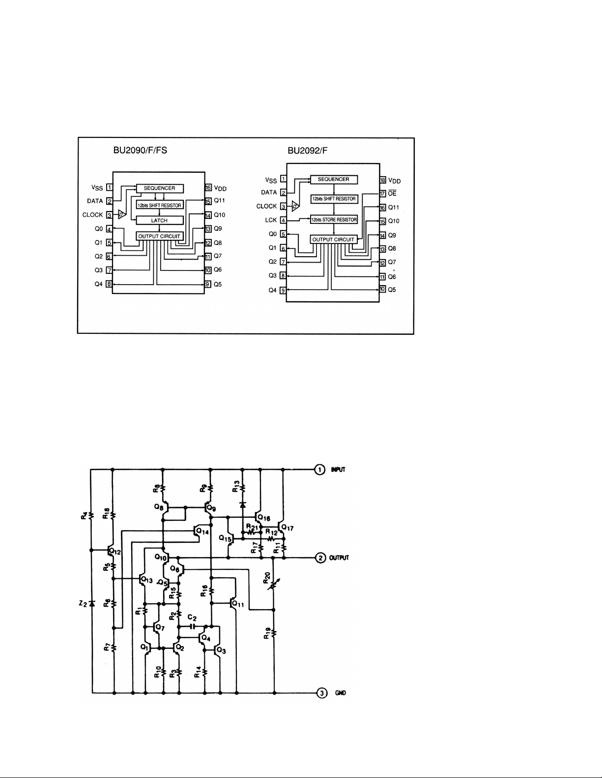
BU2090/BU2090F/BU2090FS/BU2092/BU2092F
●●
KIA78XXPI
INTERNAL BLOCK DIAGRAM OF ICs
Page 2
- 27 -
●●
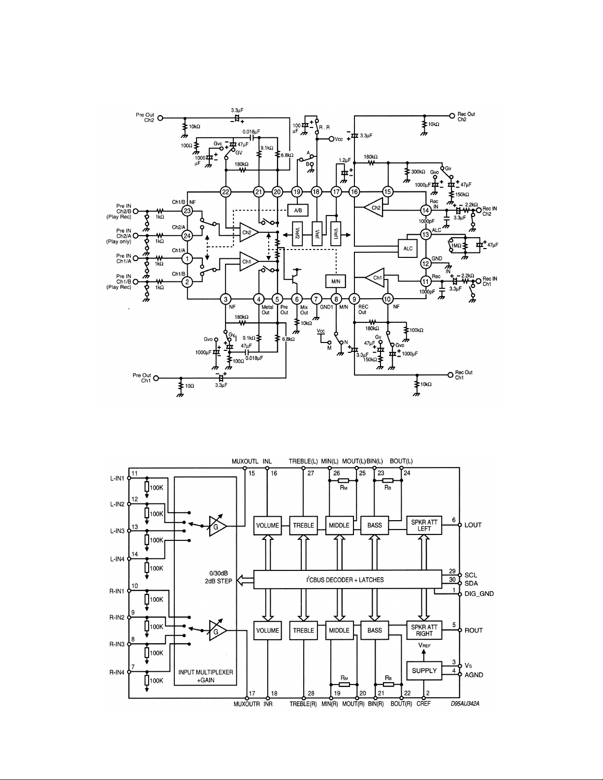
KIA6289N
●●
TDA7439
Page 3
- 28 -
●●
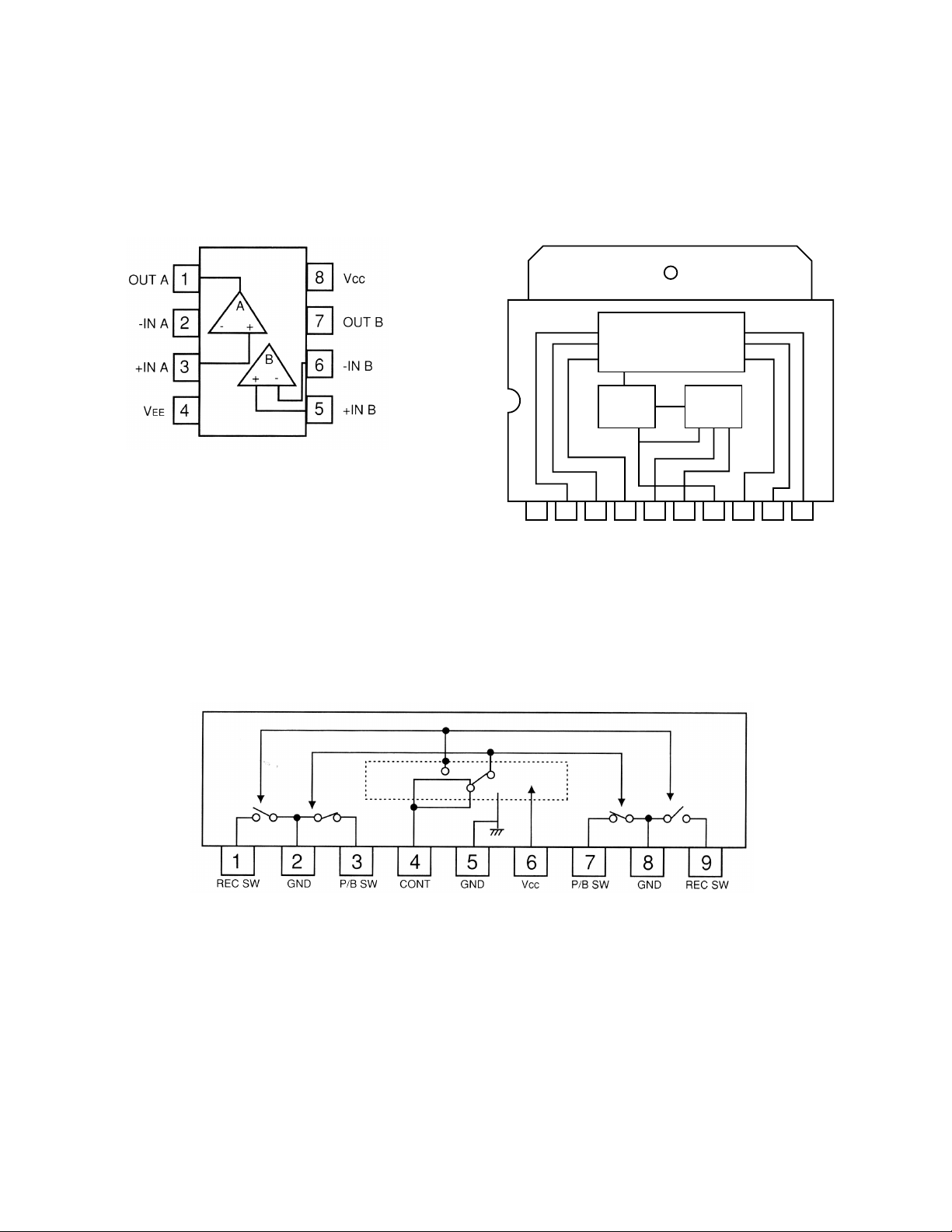
KIA4558P, KIA4558F
●●
KA8301
●●
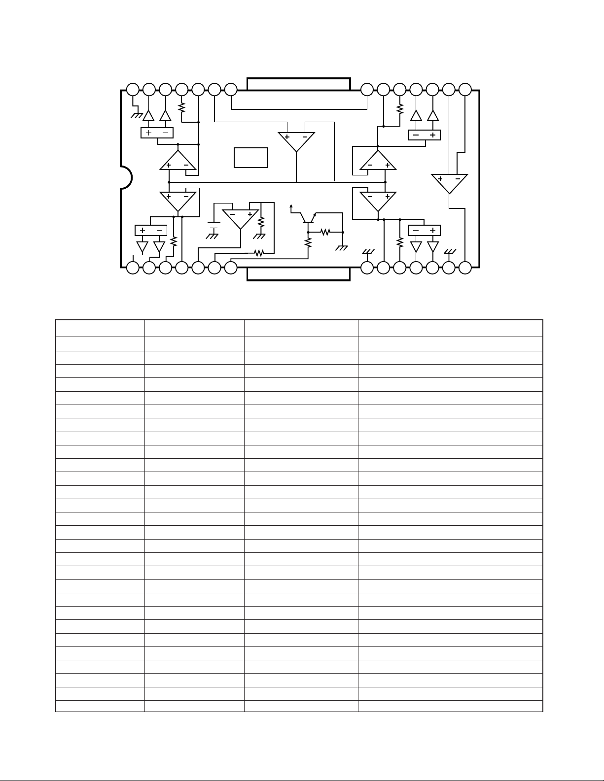
BA3126N
DRIVER
PRE
LOGIC
23456789101
GND
Vout1
Vz1VrFin
Rin
Vcc1
Vcc2
Vz2
Vout2
Page 4
- 29 -
●●
KA3010
PIN DESCRIPTION
28 27
26 25 24 23 22
T S D
REGULATOR
MUTE
LEVEL
SHIFT
LEVEL
SHIFT
100K
50K
50K
10K
10K
10K 10K
10K
BUY
BUY
BUY
LEVEL
SHIFT
LEVEL
SHIFT
1234567
8 9 10 11 12 13 14
21 20 19 18 17 16 15
Pin No. Symbol I/O Description
1 DO1.1 O DRIVE OUTPUT
2 DO1.2 O DRIVE OUTPUT
3 DI1.1 I DRIVE INPUT
4 DI1.2 I DRIVE INPUT
5 REG REGULATOR
6 REO O REGULATOR OUTPUT
7 MUTE MUTE
8 GND1 GROUND
9 DI2.1 I DRIVE INPUT
10 DI2.2 I DRIVE INPUT
11 DO2.1 O DRIVE OUTPUT
12 DO2.2 O DRIVE OUTPUT
13 GND2 GROUND
14 OPOUT O OPAMP OUTPUT
15 OPIN (-) I OPAMP OUTPUT (-)
16 OPIN (+) I OPAMP INPUT (+)
17 DO3.1 O DRIVE OUTPUT
18 DO3.2 O DRIVE OUTPUT
19 DI3.1 I DRIVE INPUT
20 DI3.2 I DRIVE INPUT
21 VCC1 SUPPLY VOLTAGE
22 VCC2 SUPPLY VOLTAGE
23 VREF 2.5V BIAS VOLTAGE
24 DI4.1 I DRIVE INPUT
25 DI4.2 I DRIVE INPUT
26 DO4.1 O DRIVE OUTPUT
27 DO4.2 O DRIVE OUTPUT
28 GND3 GROUND
Page 5

- 30 -
KB9223
MICOM TO SERVO CONTROL
AUTO SEQUENCER
FOK DETECTION
CIRCUIT
MIRROR DETECTION
CIRCUIT
Spindle Servo LPF
(Double Speed)
Sled Servo Amplifier
& Sled Kick GEN.
Tracking Phase
Compensation Block
& Jump Pulse GEN.
Focus Phase
Compensation
& Offset cancel circuit
Micom Data
Interface Logic
RF Amp
73
74
65
66
63
67
68
79
69
70
71
78
76
75
32
33
77
2
4
RF-
RFO
PD1
PD2
F
E
EI
PD
LD
VR
ARF
IRF
ASY
EFM
RFI
DCB
DCC1
GC1O
MLT
TZC
FE2
FLB
FGD
FS3
TE1
FE1
GC1I
CH1O
CH1I
MUTEI
RRC
CH2O
CH2I
GC2I
GC2O
5
15 16 13 14 19 17 12 11 9 10
40
1
39
6
25
24
23
45
46
42
44
43
61
62
55
53
50
49
57
48
47
60
FOK
MCP
MIRROR
FSET
SMEF
SMON
FS1 to
FS4
TM1 to
TM6
BAL1 to
BAL5
PS1 to
PS4
GA1 to
GA5
SMPD
SPDL-
SPDLO
SL+
SL-
SLO
TGU
TG2
LPFT
TE2
TEO
TE-
TDFCT
FEO
FE-
FDFCT
327282658525135363738312930225459
APC Amp
Center Voltage Amp.
Focus Error Amp
FE-BIAS Adjustment
Tracking Error Amp
E/F Balance & Gain
Control
RF Level AGC
&
Equalizer
EFM
Comparator
Defect Detection
CircuitT
ADJUSTMENT-FREE CONTROL
Built-in Post Filter Amp(L&R)
LDON
PIN DESCRIPTION
Pin No. System Description
1 MCP Capacitor connection pin for mirror hold
2 DCB Capacitor connection pin for defect Bottom hold
3 FRSH. Capacitor connection pin for time constant to generate focus search waveform
4 DCC2 The input pin through capacitor of defect bottom hold output
5 DCC1 The output pin of defect bottom hold
6 FSET The peak frequency setting pin for focus, tracking servo and cut off frequency of CLV LPF
7 VDDA Analog VCC for servo part
8 VCCP VCC for post filter
9 GC2I Amplifier negative input pin for gain and low pass filtering of DAC output CH2
10 GC2O Amplifier output pin for gain and low pass filtering of DAC output CH2
11 CH2I The input pin for post filter channel2
12 CH2O The output pin for post filter channel2
13 CH1O The output pin for post filter channl1
14 CH1I The input pin for post filter channel1
15 GC1O Amplifier output pin for gain and low pass filtering of DAC output CH1
Page 6

- 31 -
Pin No. System Description
16 GC1I Amplifier negative input pin for gain and low pass filtering of DAC output CH1
17 RRC The pin for noise reduction of post filter bias
18 VSSP VSS for post filter
19 MUTEI The input pin for post filter muting control
20 ISET The input pin for current setting of focus search, track jump and sled kick voltage
21 VREG The output pin of regulator
22 WDCK The clock input pin for auto sequence
23 SMDP The input pin of CLV control output pin SMDP of DSP
24 SMON The input pin for spindle servo ON through SMON of DSP
25 SMEF The input pin of provide for an external LPF time constant
26 FLB Capacitor connection pin to perform rising low bandwidth of focus loop
27 FS3 The pin for high frequency gain change of focus loop with internal FS3 switch
28 FGD Reducing high freqency gain with capacitor between FS3 pin
29 LOCK Sled runaway prevention pin
30 TRCNT Track count output pin
31 ISTAT Internal status output pin
32 ASY The input pin for asymmetry control
33 EFM EFM comparator output pin
34 VSSA Analog VSS for servo part
35 MCK Micom clock input pin
36 MDATA Micom data input pin
37 MLT Micom data latch input pin
38 RESET Reset input pin
39 MIRROR The mirror output for test
40 FOK The output pin of focus OK comparator
41 SSTOP The pin for detection whether pick_up position is innermost or not
42 SL+ The noninverting input pin of sled servo amplifier
43 SLO The output pin of sled servo amplifier
44 SL- The inverting input pin of sled servo amplifier
45 SPDL- The noninverting input pin of spindle servo amplifier
46 SPDLO The output pin of spindle servo amplifier
47 FE- The inverting input pin of focus servo amplifier
48 FEO The output pin of focus servo amplifier
49 TE- The inverting input pin of tracking servo amplifier
50 TEO The output pin of tracking servo amplifier
51 ATSC The input pin for Anti-shock detection
52 TZC The comaparator input pin for tracking zero crossing detection
53 TE2 Tracking servo input pin
54 TE1 Tracking error amplifier output pin
55 LPFT The input pin of tracking error low pass filtering signal
56 DVDD The power supply pin for logic circuit
57 TDFCT The capacitor connection pin for tracking defect compensation
58 FE2 Focus servo input pin
59 FE1 Focus error amplifier output pin
60 FDFCT The capacitor connection pin for focus defect compensation
61 TGU The capacitor connection pin for high frequency tracking gain switch
62 TG2 The pin for high frequency gain change of tracking servo loop with internal TG2 switch
63 FEBIAS Focus error bias voltage control pin
64 DVEE The DVEE pin for logic circuit
65 PD1 The negative input pin of RF I/V amplifier1 (A+C signal)
66 PD2 The negative input pin of RF I/V amplifier2 (B+D signal)
67 F The negative input pin of F I/V amplifier (F signal)
68 E The negative input pin of E I/V amplifier (E signal)
69 PD The input pin for APC
70 LD The output pin for APC
71 VR The output pin of (AVEE+AVCC)/2 voltage
72 VCC VCC for RF part
73 RF- RF summing amplifier inverting input pin
74 RFO RF summing amplifier output pin
75 IRF The input pin for AGC
76 ARF The output pin for AGC
77 RFI The input pin for EFM comparating
78 CAGC The capacitor connection pin for AGC
79 EI Feedback input pin of E I/V amplifier for EF Balance control
80 GND GND for RF part
Page 7

- 32 -
KS9286
SUBCODE
SYNC
DETECTOR
SUBCODE
OUTPUT
EFM
DEMODULATOR
8BIT DATA BUS
ADDRESS
GENERATOR
EFM
PHASE
DETECTOR
DIGITAL
PLL
DIGITAL
CLV
SERVO
CPU
INTERFACE
MODE
SELECTOR
DIGITAL
OUTPUT
D/A
CONVERTER
DIGITAL
FILTER
& DE-EMPH
INTERPOLATOR
ECC
16K
SRAM
TRACK
COUNTER
23BIT
SHIFT
REGISTER
FRAME SYNC
DETECTOR
PROTECTOR
INSERTOR
X-TAL
TIMING
GENERATOR
SUBCODE-Q
REGISTER
SQDT
30
29
11
66
5
3
4
2
72
73
75
76
70
9
8
37
38
36
616263
65
7
19
20
33
32
26
69
68
12
14
77
67
60
24
17
22
SDAT
SBCK
S0S1
LRCHO
ADATAO
BCKO
BCKI
ADATAI
LRCHI
EMPH
VREFL1
VREFH1
EFMI
CNTVOL
DPFIN
DPFOUT
DPDO
SMEF
SMON
SMDP
SMSD
LOCK
XOUT
LCHOUT
RCHOUT
DATX
TEST1
TEST0
XTALSEL
CDROM
XIN
MDAT
MCK
MLT
TRCNT
/ISTAT
SQCK
PIN DESCRIPTION
Pin No. Symbol IO Description
1 AVDD1 - Analog VCC1
2 DPDO O Charge pump output for Digital PLL
3 DPFIN I Filter input for Digital PLL
4 DPFOUT O Filter output for Digital PLL
5 CNTVOL I VCO control voltage for Digital PLL
6 AVSS1 - Analog Ground1
7 DATX O Digital Audio output data
8 XIN I X’tal oscillator input
9 XOUT O X’tal oscillator output
10 WDCHO O Word clock output of 48bit/Slot (88.2KHz)
11 LRCHO O Channel clock output of 48 bit/Slot (44.1KHz), 88.2KHz when ESP ON
12 ADATAO O Serial audio data output of 48 bit/Slot (MSB first), double speed output when ESP ON
13 DVSS1 - Digital Ground1
14 BCKO O Audio data bit clock output of 48 bit/Slot (2.1168MHz), 4.2336MHz when ESP ON
15 C2PO O C2 Pointer for output audio data
16 VREFL2 I Input terminal2 of reference voltage “L”(Floating)
Page 8

- 33 -
Pin No. Symbol IO Description
17 VREFL1 I Input terminal1 of reference voltage “L”(GND connection)
18 AVDD2 - Analog VCC2
19 RCHOUT O Right-Channel audio output through D/A converter
20 LCHOUT O Left-Channel audio output through D/A converter
21 AVSS2 - Analog ground2
22 VREFH1 I Input terminal1 of reference voltage “H”(VDD connection)
23 VREFH2 I Input terminal2 of reference voltage “H”(Floating)
24 EMPH O Emphasis/Non-Emphasis output, H: Emphasis ON, L: Emphasis OFF
25 LKFS O The Lock Status output of frame sync
26 S0S1 O Output of subcode sync signal (S0+S1)
27 RESET I System reset at “L”
28 /ESP I ESP function ON/OFF control (“L”: ESP function ON, “H”: ESP function OFF)
29 SQCK I Clock for output Subcode-Q data
30 SQDT O Serial output of Subcode-Q data
31 SQOK O The CRC (Cycle Redundancy Check) check result signal output of Subcode-Q
32 SBCK I Clock for output subcode data
33 SDAT O Subcode serial data output
34 DVDD1 - Digital VDD1
35 MUTE I Mute control input (“H”: Mute ON)
36 MLT I Latch Signal Input from Micom (Scmit Trigger)
37 MDAT I Signal data input from Micom (Scmit Trigger)
38 MCK I Signal clock Input from Micom (Scmit Trigger)
39 DB8 I/O SRAM data I/O port 8 (MSB)
40 DB7 I/O SRAM data I/O port 7
41 DB6 I/O SRAM data I/O port 6
42 DB5 I/O SRAM data I/O port 5
43 DB4 I/O SRAM data I/O port 4
44 DB3 I/O SRAM data I/O port 3
45 DB2 I/O SRAM data I/O port 2
46 DB1 I/O SRAM data I/O port 1 (LSB)
47 C1F1 I/O Monitoring output for C1 error correction (RA1)
48 C1F2 I/O Monitoring output for C1 error correction (RA2)
49 C2F1 I/O Monitoring output for C2 error correction (RA3)
50 C2F2 I/O Monitoring output for C2 error correction (RA4)
51 C2FL I/O C2 decoder flag (RA5, “H”: When one processing C2 code is impossible correction status.)
52 /PBCK I/O Output of VCO/2 (4.3218MHz) (RA6)
53 DVSS2 I/O Digital ground 2
54 FSDW I/O Window or unprotected frame sync (RA7)
55 ULKFS I/O Frame sync protection state (RA8)
56 /JIT I/O Display of either RAM overflow onncerflow for ±4 frame jitter margin (RA9)
57 C4M I/O Only monitoring signal (4.2336M .. RA10)
58 C16M I/O 16.9344MHz signal output (RA11)
59 /WE I/O Terminal for test
60 /CS I/O Terminal for test
61 XTALSEL I Mode Selection1 (H: 33.8688MHz, L: 16.9344MHz)
62 TEST0 I TEST input terminal (GND connection)
63 CDROM I Mode Selection2 (H: CD-ROM, L: CDP)
64 SRAM I TEST input terminal (GND connection)
65 TEST1 I TEST input terminal (GND connection)
66 EFMI I EFM signal input
67 ADATAI I Serial audio data input of 48 bit/Slot (MSB first)
68 /ISTAT O The internal status output
69 TRCNT I Tracking counter input signal
70 LOCK O Output signal of LKFS condition sampled PBFR/16 (if LKFS is “H”, LOCK is “H”, if LKFS is sampled
“L”at least 8 times by PBFR/16, LOCK is “L”.)
71 PBFR O Write frame clock (Lock: 7.35KHz)
72 SMEF O LPF time constant control of the spindle servo error signal
73 SMON O ON/OFF control signal for spindle servo
74 DVDD2 - Digital VDD2
75 SMDP O Spindle Motor drive (Rough control in the SPEED mode, Phase control in the PHASE mode)
76 SMSD O Spindle Motor drive (Velocity control in the PHASE mode)
77 BCKI I Audio data bit clock input of 48 bit/Slot (2.1168MHz)
78 TESTV I TEST input terminal (GND connection)
79 DSPEED I TEST input terminal (VDD connection)
80 LRCHI I Channel clock input of 48 bit/Slot (44.1KHz)
Page 9

- 34 -
LC72131
LA1837
LC72131M
Page 10

- 35 -
MSGEQ7
PIN CONFIGURATION
PIN DESCRIPTION
Page 11

- 36 -
STK411-220E
 Loading...