

Page 1

FCC Compliance Statement:
This equipment has been tested and found to
comply with limits for a Class B digital device,
pursuant to Part 15 of the FCC rules. These
limits are designed to provide reasonable
protection against harmful interference in
residential installations. This equipment
generates, uses, and can radiate radio
frequency energy, and if not installed and used
in accordance with the instructio ns, may cause
harmful interference to radio communications.
However, there is no g uara nte e that interference
will not occur in a particular installation. If this
equipment does cause interference to radio or
television equipment reception, which can be
determined by tur ning th e equi pment off and on, the us er is e ncourage d to try t o
correct the interference by one or more of the following measures:
-Reorient or relocate the receiving antenna
-Move the equipment away from the receiver
-Plug the equipment into an outlet on a circuit different from that to which
the receiver is connected
-Consult the dealer or an experienced radio/television technician for
additional suggestions
You are cautioned that any change or modifications to the equipment not
expressly approve by the party responsible for compliance could void Your
authority to operate such equipment.
This device complies with Part 15 of the FCC Rules. Operation is subjected to
the following two conditions 1) this device may not cause harmful interference
and 2) this device mu st a cc ept any interference received , in cl uding interference
that may cause undesired operation.
DECLARATION OF CONFORMITY
Per FCC Part 2 Section 2. 1077(a)
Responsible Party Name: G .B.T. INC.
Add ress: 18305 Val l ey Bl vd., Suite#A
LA Puent, CA 91744
Phone/Fax No: (818 ) 854-9338/ (818) 854-9339
hereby declares that the product
Product Name:
Model Number:
Mother Board
Conforms to the following specificati ons:
FCC Part 15, Sub part B, Sect ion 15.107(a) and Section 15 .109(a),
Class B Digital Device
Suppleme ntary Info rmati on:
This device complies with part 15 of the FCC Rules. Operation is subject to the
following two c onditio ns: (1) This device may not cause harmful
and (2) this device must accept any inference received, includin g
that may cause undesired operati on.
Representative Person's Name: ERIC LU
Signatur e:
Date: Jul. 20, 2000
Eric Lu
GA-6 VXDC7
Page 2

Declaration of Conformity
We, Manufacturer/Importer
(full address)
G.B.T. Technology Träding GMbH
Ausschlager Weg 41, 1F, 20537 Hamburg, Germany
declare that the product
( description of the apparatus, system, installation to which it refer s)
Mother Board
GA-6VXDC7
is in conformity with
(reference to the specification under which conformity is declared)
in accordance with 89/336 EEC-EMC Directive
EN 55011
Limits and methods of measurement
EN 61000-3-2*
Disturbances in supply systems caused
of radio disturbance characteristics of
EN60555-2
by household appliances and sim ilar
industrial, scientific and medical (ISM electrical equipment “Harmoni c s”
high frequency equipment
EN55013
Limits and methods of measurement
EN61000-3-3*
Disturbances in supply systems caused
of radio disturbance characteristics of
EN60555-3
by household appliances and sim ilar
broadcast receivers and associated electrical equipment “Voltage fluctuat ions”
equipment
EN 55014
Limits and methods of measurement
EN 50081-1
Generic emission standard Part 1:
of radio disturbance characteristics of
Residual, commercial and light industry
household electric al appliances,
portable tools and similar elec trical
EN 50082-1
Generic immunity standar d P ar t 1:
apparatus Residual, commercial and light industry
EN 55015
Limits and methods of measurement
EN 55081-2
Generic emission standard Part 2:
of radio disturbance characteristics of Industrial environment
fluorescent lamps and lumi nar ies
EN 55020
Immunity from radio interferenc e of
EN 55082-2
Generic immunity standar d P ar t 2:
broadcast receivers and associated Industrial environment
equipment
EN 55022
Limits and methods of measurement
ENV 55104
Immunity requir ements for household
of radio disturbance characteristics of appliances tools and similar apparatus
inform ation technology equipment
DIN VDE 0855
Cabled distribut ion systems; Equipment
EN 50091- 2
EMC requirement s for uninterrupt ible
part 10
for receiving and/or
distribution
from power systems (UPS)
part 12
sound and television signals
CE marking
(EC conformity mark ing)
The manufacturer also declares the conformity of above mentioned product
with the actual required safet y standards in acco rdance with LVD 73/23 EEC
EN 60065
Safety requirem ents for mains operated
EN 60950
Safety for information technology equipment
electronic and r elated apparatus for including elec trical business equipment
household and simil ar gener al use
EN 60335
Safety of household and similar
EN 50091-1
General and Safety requirements for
electrical appliances uninterruptible power systems (UPS)
Manufacturer/Importer
Signature
:
Rex Lin
(Stamp)
Date : Jul. 20, 2000 Name : Rex Lin
Page 3

6VXDC7
Socket 370 Processor Motherboard
USER'S MANUAL
Socket 370 Processor Motherboard
REV. 1.0 Third Edition
R-10-03-010622
12ME-6VXDC7-1003
Page 4

Page 5

How This Manual Is Organized
This manual is divided into the following sections:
1) Revision History
Manual revision information
2) Item Checklist
Product item list
3) Features
Product information & specification
4) Hardware Setup
Instructions on setting up the motherboard
5) Performance & Block Diagram
Product performance & block diagram
6) Dual BIOS & Suspend to RAM
Instruction Dual BIOS & STR installation
7) Four Speaker & SPDIF
Four Speaker & SPDIF introduction
8) BIOS Setup
Instructions on setting up the BIOS
software
9) Appendix
General reference
Page 6

Page 7

Table Of Content
Revision History P.1
Item Checklist P.2
Summary of Features P.3
6VXDC7 Motherboard Layout P.5
Page Index for CPU Speed Setup/Connectors/Panel and Jumper Definition P.6
Performance List P.28
Block Diagram P.29
Suspend to RAM Installation P.30
Dual BIOS Introduction (Optional) P.36
Four Speaker & SPDIF Introduction (Optional) P.43
Memory Installation P.48
Page Index for BIOS Setup P.49
Appendix P.77
Page 8

6VXDC7 Motherboard
1
Revision History
Revision Revision Note Date
1.0 Initial release of the 6VXDC7 motherboard user’s manual. Aug.2000
1.0 Second release of the 6VXDC7 motherboard user’s
manual.
Aug.2000
1.0 Third release of the 6VXDC7 motherboard user’s manual. Jun.2001
The author assumes no responsibility for any errors or omissions that may appear in this
document nor does the author make a commitment to update the information contained herein.
Third-party brands and names are the property of their respective owners.
Jun. 22, 2001 Taipei, Taiwan, R.O.C
Page 9

Item Check l i st
2
Item Checklist
;
The 6VXDC7 motherboard
;
Cable for IDE / floppy device
;
Diskettes or CD (TUCD) for motherboard driver & utility
;
6VXDC7 user’s manual
Page 10

6VXDC7 Motherboard
3
Summary Of Features
Form Factor
y
30.4 cm x 24.3 cm AT X size form factor, 4 layers PCB.
CPU
y
2 Socket 370 processor
Intel Pentium
!!!
100/133MHz FSB, FC-PGA
Intel Celeron
TM
66MHz FSB, FC-PGA (Only support single CPU)
y
2nd cache in CPU (Depend on CPU)
Chipset
y
VT82C694X (VIA Apollo Pro 133A)
y
VT82C686A
Clock Generator
y
ICS 9248AF-63
y
66/100/133 MHz system bus speeds (PCI 33MHz)
y
112/124/133/142/152 MHz system bus speeds
(PCI 44MHz) (reserved)
Memory
y
4 168-pin DIMM sockets
y
Supports PC-100 / PC-133 SDRAM and VCM SDRAM
y
Supports up to 1.5GB DRAM (Max)
y
Supports only 3.3V SDRAM DIMM
y
Supports 72bit ECC type DRAM integrity mode
I/O Control
y
VT82C686A
Slots
y
1 AGP slot supports 2X/4X mode & AGP 2.0
compliant
y
5 PCI slot supports 33MHz & PCI 2.2 compliant
y
1 16-bit ISA Bus slots
On-Board IDE
y
2 IDE bus master (DMA 33/ ATA 66 )IDE ports for up
to 4 ATAPI devices
y
Supports PIO mode 3, 4 (UDMA 33/ATA 66) IDE &
ATAPI CD-ROM
On-Board
Peripherals
y
1 floppy port supports 2 FDD with 360K, 720K, 1.2M,
1.44M and 2.88M bytes
y
1 parallel ports supports Normal/EPP/ECP mode
y
2 serial ports (COM 1 & COM 2)
y
4 USB ports
y
1 IrDA connector for Fast IrDA
To be continued…
Page 11

Summary of Features
4
Hardware Monitor
y
CPU1 / CPU2 Fan revolution detect
y
CPU1 / CPU2 temperature detect
y
System voltage detect
y
CPU overheat shutdown detect
PS/2 Connector
y
PS/2 Keyboard interface and PS/2 Mouse interface
BIOS
y
Licensed AMI BIOS, 2M bit flash ROM
y
Support Dual BIOS (Optional)
On-Board Sound
(Optional)
y
Creative CT5880 sound
y
AC’97 CODEC
y
Line In / Line Out / Mic In / AUX In / CD In / TEL /
Game Port /Four Speaker & SPDIF
Additional Features
y
Support Wake-On-LAN (WOL)
y
Support Internal / External Modem Ring On
y
Includes 4 fan power connectors
y
Poly fuse for keyboard over-current protection
y
Supported Suspend to RAM (STR)
Page 12

6VXDC7 Motherboard
5
6VXDC7 Motherboard Layout
PCI2
PCI3
VT82C686A
GAME & AUDIO
COM 2
COM 1
LPT
PS/2
SW2
PCI4
PCI5
ISA
DIMM3
DIMM2
SW1
AGP
J16
6VXDC7
PCI1
BAT1
PGA 370
CPU 2
J15
USB
ATX Power
Floppy
IDE1
IDE2
Main
BIOS
J8
J7
J5
VT82C694X
AD1881
DIMM4
DIMM1
PGA 370
CPU 1
JP9
JP25
J13
JP1
J14
USB2
J1
J3
J4
Back
BIOS
JP20
CT5880
J2
JP5
LED1
JP11
Page 13

6VXDC7 Motherboard Layout
6
Page Index for CPU Speed Setup/Connectors/Panel and Jumper Definition
Page
CPU Speed Setup P.7
Connectors P.14
Game & Audio Port [Optional] P.14
COM 1 / COM 2 / LPT Port P.14
USB 1 Connector P.15
PS/2 Keyboard & PS/2 Mouse Connector P.15
J13 (CPU 1 Fan) P.16
J15 (CPU 2 Fan) P.16
J16 (Power Fan) P.17
J14 (System Fan) P.17
ATX Power P.18
Floppy Port P.18
IDE 1(Primary) / IDE 2(Secondary) Port P.19
J7 (TEL) [Optional] P.19
J5 (AUX_IN) [Optional] P.20
J8 (CD Audio Line In) [Optional] P.20
J3 (Ring Power On) P.21
J1 (Wake On LAN) P.21
J4 (IR) P.22
USB 2 Connector P.22
JP5 / LED1(STR LED Connector & DIMM LED) P.23
Panel and Jumper Definition P.24
J2 (2x11 Pins Jumper) P.24
JP1 (Clear CMOS Function) P.25
JP20 (Onboard Sound Function Selection)[Optional] P.25
JP9 (USB Device Wake Up Selection) P.26
JP11 (STR Function Enabled) P.26
BAT1 (Battery) P.27
Page 14

6VXDC7 Motherboard
7
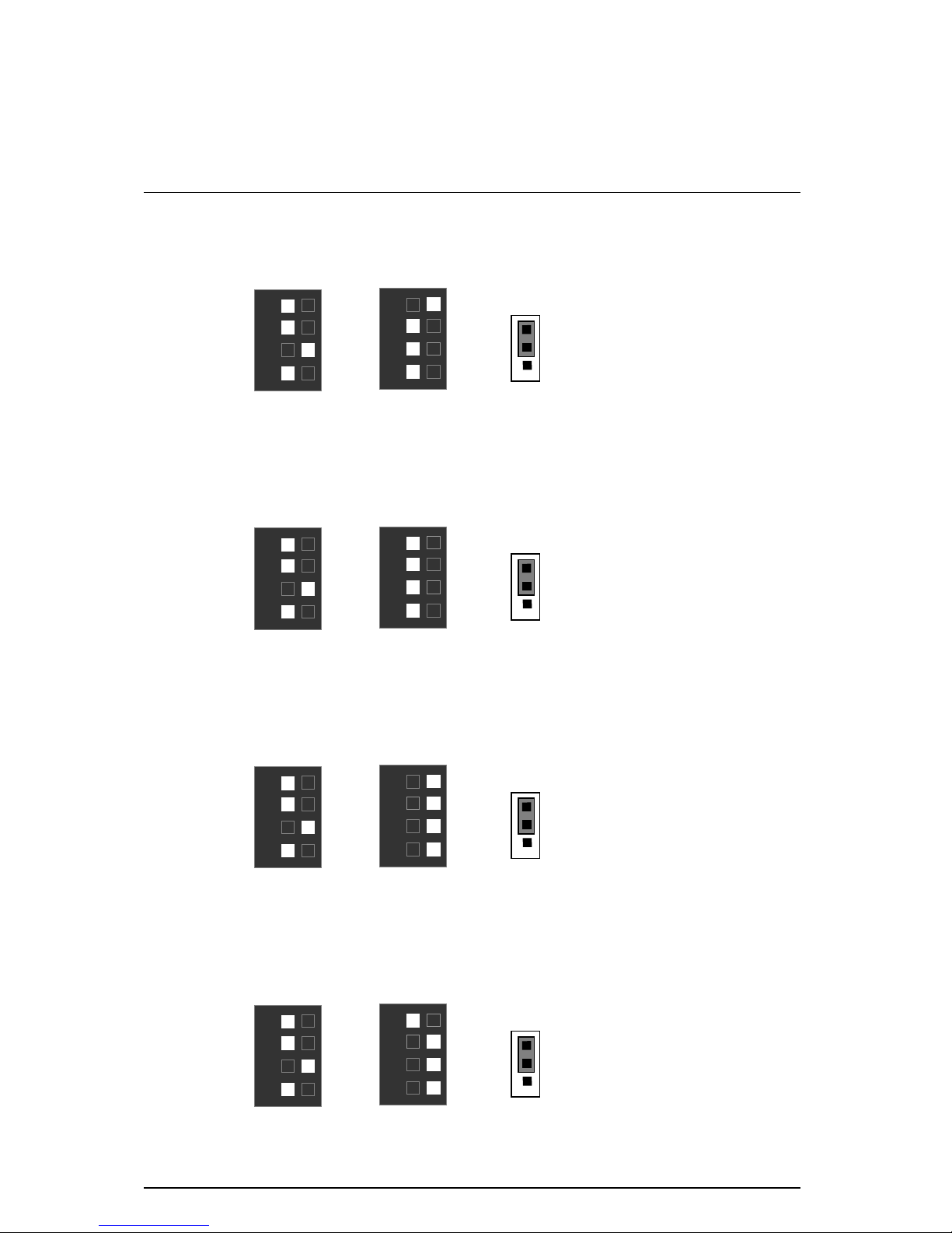
CPU Speed Setup
The system bus speed is selectable at 66,100,133MHz. The user can s elect the system bus
speed
(SW1)
and change the DIP switch
(SW2)
selection to set up the CPU speed for
500MHz – 1GHz and faster processor.
Set System Bus Speed
SW1/JP25:
O : ON, X : OFF
1 2 3 JP25 CPU(MHz) PCI(MHz)
X X O 1-2 66 33
X X X 1-2 100 33
O X X 1-2 112 37
O O X 1-2 124 41
O O O N/C 133 33
X O O N/C 142 35
O X O N/C 152 38
The CPU speed must m atch with the frequency ratio. It will cause system hanging up if
the frequency ratio is higher than that of CPU.
DIP SWITCH
SW2:FREQ. RATIO
1 2 3 4
X 3
O
X O O
X 3.5
X X O O
X 4
O O X O
X 4.5
X O
X O
X 5
O X X O
X 5.5
X X X O
X 6
O O O X
X 6.5
X O O X
X 7
O X O X
X 7.5
X X O X
X 8
O O X X
X 8.5
O X O O
X 9
X X O O
X 9.5
X O O O
X 10
X O X X
X 10.5
O O X O
X11
O X X X
X11.5
X O X O
Page 15

CPU Speed Setup
8
X12
O X X O
X13
X X X O
X14
O O O X
X15
X O O X
X16
O X O X
0000
Intel Processor all have locked Frequency Multiple, so yo u can not change the CPU
Frequency Multiple.
0000
For double CPU use, the same CPU m ust be used in CP U socket1 and 2. (The same
stepping, FSB, ratio)
0000
For single CPU use, use CPU socket1 only. Don’t use CPU socket2.
Note: We don’t recommend you to set up your system speed to 112 , 124 , 142 ,152 MHz
because these frequencies are not the standard specifications for CPU, Chipset and
most of the peripherals. Whether your system can run under 112 ,124 ,142 ,152 MHz
properly will depend on your hardware configurations: CPU, SDRAM, Cards, etc.
1. CeleronTM 533/66MHz
SW2
SW2
1 2 3 4
SW2
ON
SW1
1 2 3 4
1
JP25
2. CeleronTM 566/66MHz
SW2
ON
1 2 3 4
SW1
ON
1 2 3 4
1
JP25
Page 16
6VXDC7 Motherboard
9
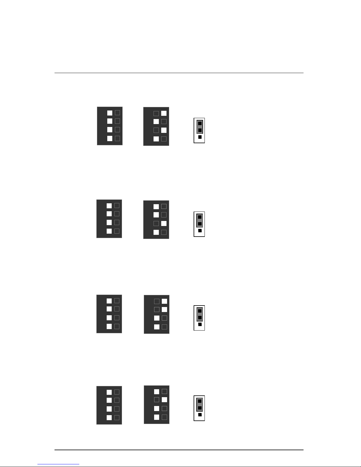
3. CeleronTM 600/66MHz
SW2
ON
1 2 3 4
1
JP25
SW1
ON
1 2 3 4
4. CeleronTM 633/66MHz
SW2
ON
1 2 3 4
1
JP25
SW1
ON
1 2 3 4
5. CeleronTM 667/66MHz
SW2
ON
1 2 3 4
1
JP25
SW1
ON
1 2 3 4
6. CeleronTM 700/66MHz
SW2
ON
1 2 3 4
1
JP25
SW1
ON
1 2 3 4
Page 17

CPU Speed Setup
10
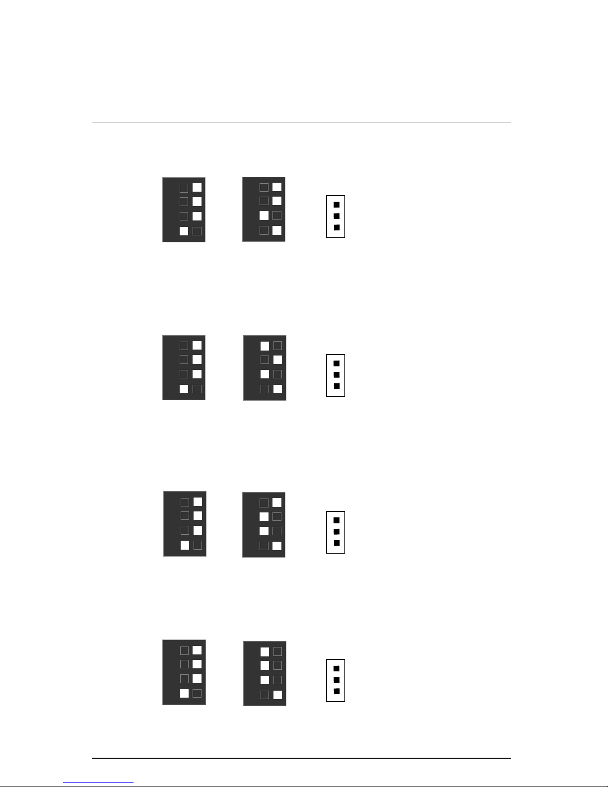
7. Pentium
!!!
500/100MHz FSB
SW2
ON
1 2 3 4
SW1
ON
1 2 3 4
1
JP25
8. Pentium
!!!
550/100MHz FSB
SW2
ON
1 2 3 4
SW1
ON
1 2 3 4
1
JP25
9. Pentium
!!!
600/100MHz FSB
SW2
ON
1 2 3 4
SW1
ON
1 2 3 4
1
JP25
10. Pentium
!!!
650/100MHz FSB
SW2
ON
1 2 3 4
SW1
ON
1 2 3 4
1
JP25
Page 18
6VXDC7 Motherboard
11
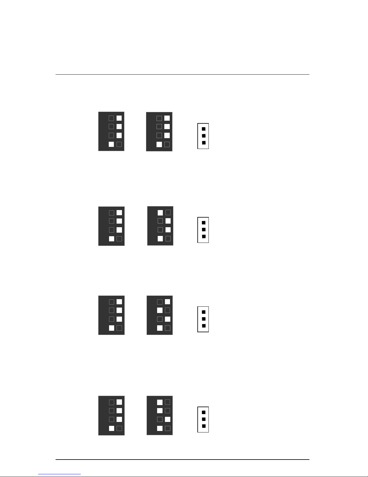
11. Pentium
!!!
700/100MHz FSB
SW2
ON
1 2 3 4
SW1
ON
1 2 3 4
1
JP25
12. Pentium
!!!
750/100MHz FSB
SW2
ON
1 2 3 4
SW1
ON
1 2 3 4
1
JP25
13. Pentium
!!!
800/100MHz FSB
SW2
ON
1 2 3 4
SW1
ON
1 2 3 4
1
JP25
14. Pentium
!!!
850/100MHz FSB
SW2
ON
1 2 3 4
SW1
ON
1 2 3 4
1
JP25
Page 19
CPU Speed Setup
12
15. Pentium
!!!
533/133MHz FSB
SW2
ON
1 2 3 4
SW1
ON
1 2 3 4
1
JP25
16. Pentium
!!!
600/133 MHz FSB
SW2
ON
1 2 3 4
SW1
ON
1 2 3 4
1
JP25
17. Pentium
!!!
667/133MHz FSB
SW2
ON
1 2 3 4
SW1
ON
1 2 3 4
1
JP25
18. Pentium
!!!
733/133MHz FSB
SW2
ON
1 2 3 4
SW1
ON
1 2 3 4
1
JP25
Page 20
6VXDC7 Motherboard
13
19. Pentium
!!!
800/133MHz FSB
SW2
ON
1 2 3 4
SW1
ON
1 2 3 4
1
JP25
20. Pentium
!!!
866/133MHz FSB
SW2
ON
1 2 3 4
SW1
ON
1 2 3 4
1
JP25
21. Pentium
!!!
933/133MHz FSB
SW2
ON
1 2 3 4
SW1
ON
1 2 3 4
1
JP25
22. Pentium
!!!
1GHz/133MHz FSB
SW2
ON
1 2 3 4
SW1
ON
1 2 3 4
1
JP25
Page 21
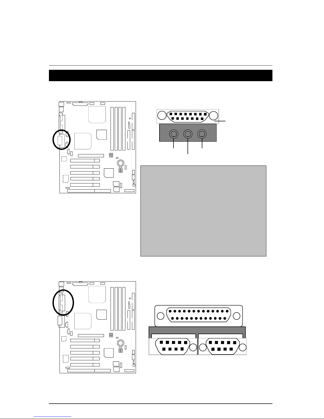
Connectors
14
Connectors
Game & Audio Port (Optional)
Line Out 1: Line Out or SPDIF (The SPDIF output
is capable of providing digital audio to external
speakers or compressed AC3 data to an external
Dolby digital decoder). In general, Line Out 1 is
normally Line Out, when it output digital signal, it
will be change to SPDIF Out automatically (see
page 45 for more information).
Line In: In general, Line In is normally Line In.
When you select “Four Speaker” in Creative
application(see page 43 for more information),
Line In will be change to Line Out 2, then you can
plug 2 pairs stereo speaker into Line Out 1 and
Line In simultaneously.
MIC In
Game
Port
Line In
Line Out 1
COM 1 / COM 2 / LPT Port
COM 1
LPT Port
COM 2
Page 22

6VXDC7 Motherboard
15
USB 1 Connector
Pin No. Definition
1 USB V0
2 USB D03 USB D0+
4 GND
5 USB V1
6 USB D17 USB D1+
8 GND
1 2
3
4
8
7
6 5
PS/2 Keyboard & PS/2 Mouse Connector
PS/2 Mouse/
Keyboard
Pin No. Definition
1 Data
2 NC
3 GND
4 VCC(+5V)
5 Clock
6 NC
PS/2 Keyboard
PS/2 Mouse
1
2
3
4
5
6
Page 23

Connectors
16
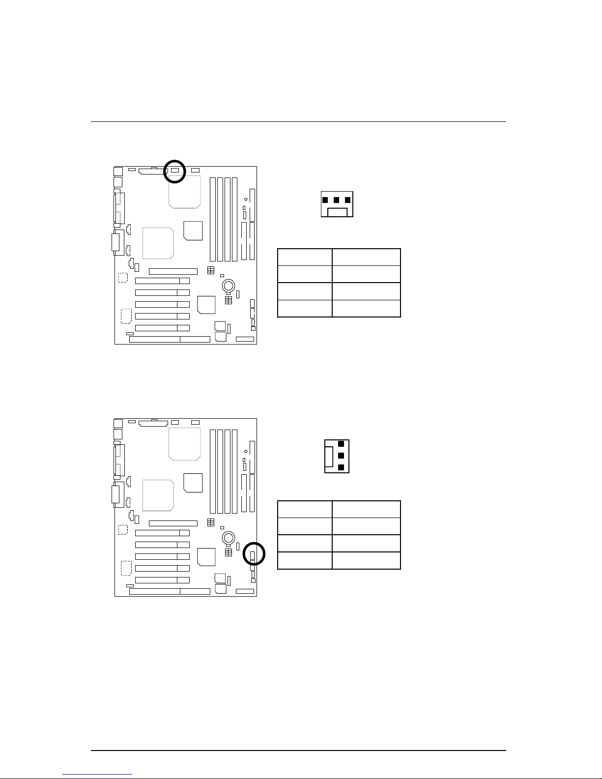
J13 : CPU1 Fan
Pin No. Definition
1 Control
2 +12V
3 SENSE
1
J15 : CPU2 Fan
Pin No. Defin itio n
1 Control
2 +12V
3 SENSE
1
Page 24
6VXDC7 Motherboard
17
J16 : Power Fan
Pin No. Definition
1 Control
2 +12V
3 NC
1
J14 : System Fan
Pin No. Definition
1 Control
2 +12V
3 NC
1
Page 25

Connectors
18
ATX Power
Pin No. Definition
3,5,7,13,
15-17
GND
1,2,11 3.3V
4,6,19,20 VCC
10 +12V
12 -12V
18 -5V
8 Power Good
9 5V SB stand by+5V
14 PS-ON(Soft On/Off)
20
10
11
1
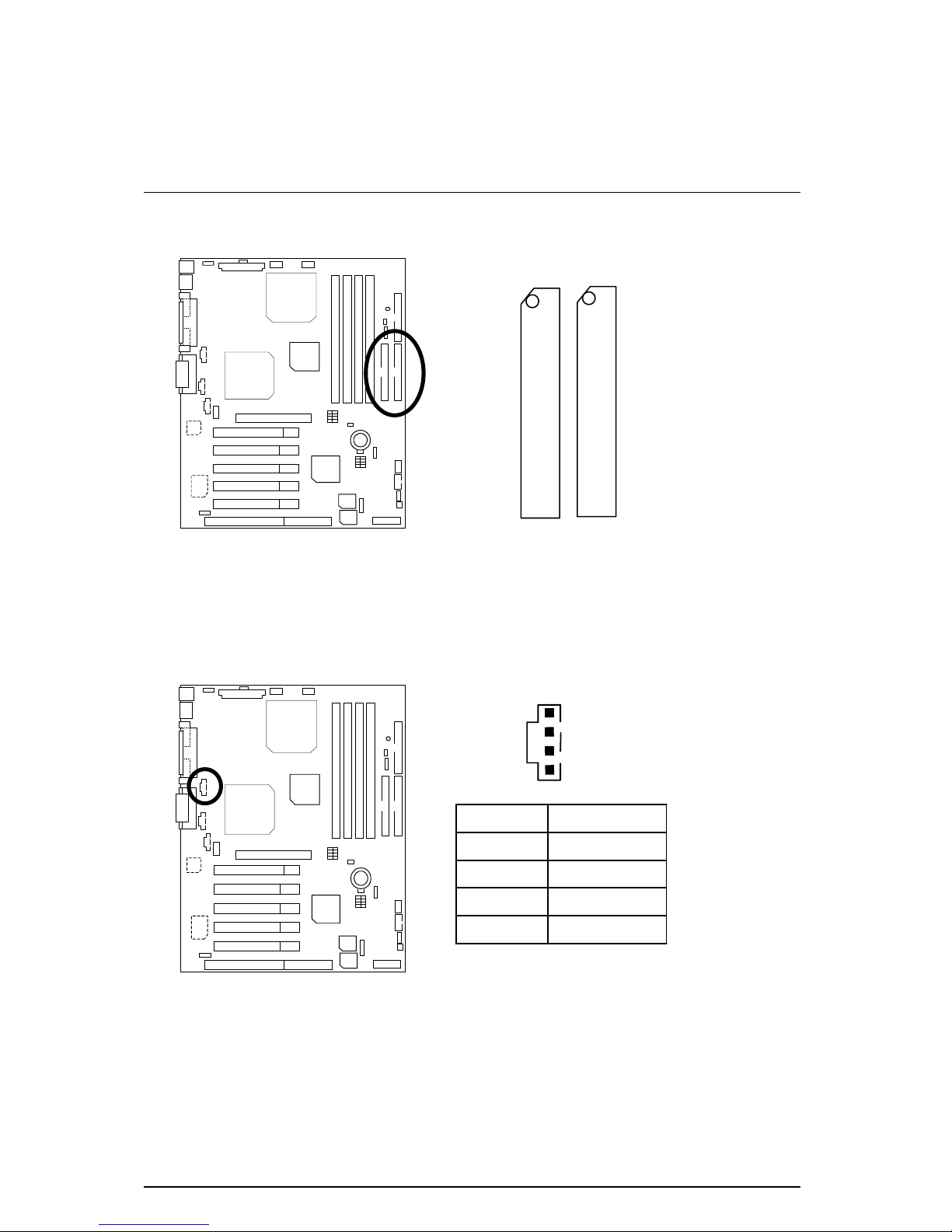
Floppy Port
Red Line
FDD1
Page 26
6VXDC7 Motherboard
19
IDE1 (Primary), IDE2 (Secondary) Port
IDE 1 IDE 2
Red Line
J7 TEL : The connector is for Modem with internal voice connector
(Optional)
Pin No. Defin itio n
1 Signal-In
2 GND
3 GND
4 Signal-Out
1
Page 27
Connectors
20
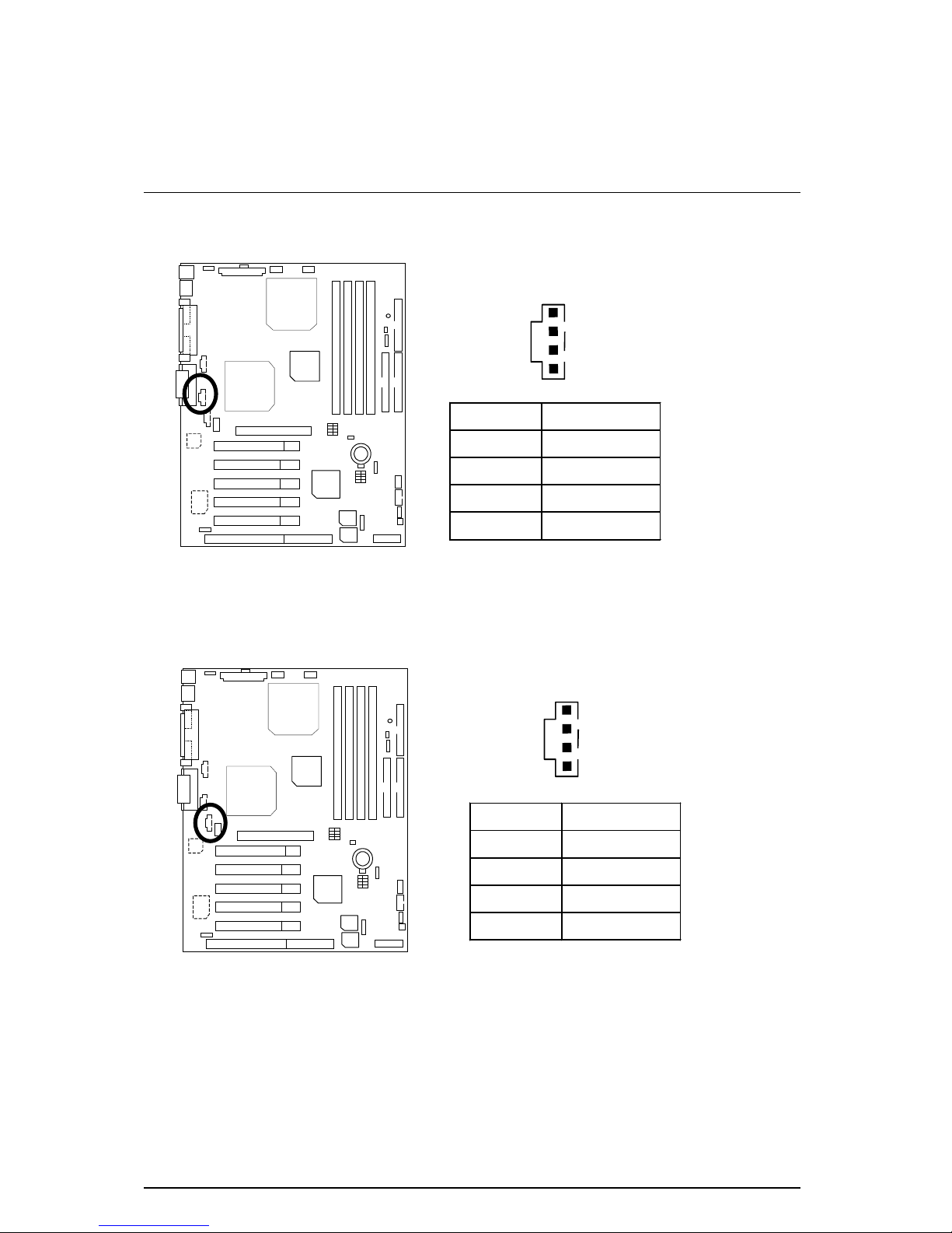
J5 : AUX_IN (Optional)
Pin No. Definition
1 AUX-L
2 GND
3 GND
4 AUX-R
1
J8 : CD Audio Line In (Optional)
Pin No. Definition
1 CD-L
2 GND
3 GND
4 CD-R
1
Page 28

6VXDC7 Motherboard
21
J3 : Ring Power On (Internal Modem Card Wa ke Up)
Pin No. Definition
1 Signal
2 GND
1
J1 : Wake On LAN
Pin No. Definition
1 +5V SB
2 GND
3 Signal
1
Page 29

Connectors
22
J4 : IR
Pin No. Definition
1 VCC (+5V)
2 NC
3 IR Data Inpu t
4 GND
5 IR Data Output
1
USB 2 Connector
1
9
2
10
Pin No. Definition
1,10 +5V
2,9 GND
3 USB D2-
4,7 NC
5 USB D2+
6 USB D3+
8 USB D3-
Page 30

6VXDC7 Motherboard
23
JP5 : STR LED Connector & LED1 : DIMM LED
1
+
DIMM LED
STR LED C onnector External.
Page 31

Panel and Jumper Definition
24
Panel And Jumper Definition
J2 : 2x11 Pins Jumper
RE
GN GD PW
P+ P− P−
S P K
HD
1
1
1
GN (Green Switch) Open: Normal Operation
Close: Entering Green Mode
GD (Green LED) Pin 1: LED anode(+)
Pin 2: LED cathode(−)
HD (IDE Hard Disk Active LED) Pin 1: LED anode(+)
Pin 2: LED cathode(−)
SPK (Speaker Connector) Pin 1: VCC(+)
Pin 2- Pin 3: NC
Pin 4: Data(−)
RE (Reset Switch) Open: Normal Operation
Close: Reset Hardware System
P+P−P−(Power LED)
Pin 1: LED anode(+)
Pin 2: LED cathode(−)
Pin 3: LED cathode(−)
PW (Soft Power Connector) Open: Normal Operation
Close: Power On/Off
Page 32

6VXDC7 Motherboard
25
JP1 : Clear CMOS Function
1
Pin No. Definition
1-2 Close Normal (Default)
2-3 Close Clear CMOS
JP20 : Onboard Sound Function Selection (Optional)
Pin No . Defin itio n
1-2 close
Enabled Onboard sound
(Default)
2-3 close Disabled Onboard sound
1
Page 33

Panel and Jumper Definition
26
JP9 : USB device Wake up Selection
1
Pin No . Defin itio n
1-2 close Normal (Default)
2-3 close
Enabled USB Device
Wake up
JP11 : STR Function Enabled
Pin No. Definition
open STR Disabled
(Default)
close STR Enabled
1
Page 34

6VXDC7 Motherboard
27
BAT1 : Battery
+
☞
Danger of explosion if battery
is incorrectly replaced.
☞
Replace only with the same or
equivalent type recommended
by the manufacturer.
☞
Dispose of used batteries
according to the manufacturer’s
instructions.
Page 35

Performance List
28
Performance List
The following performance data list is the testing results of some popular benchmark testing
programs.
These data are just referred by users, and there is no responsibility for different testing data
values gotten by users. (The different Hardware & Software configuration will result in different
benchmark testing results.)
•
CPU
Intel® Pentium III Processor 866MHz*2
•
DRAM
128MB*3 (MICRON 9920 MT 48LC8M8A2-75B)
•
CACHE SIZE
256KB include in CPU
•
DISPLAY
GA-MG400
•
STORAGE
Onboard IDE (Maxtor 93073U6)
•
O.S.
Windows NTTM 4.0 SPK6a
•
DRIVER
Display Driver at 1024x768x16bitx75MHz
Processor
Intel® Pentium III Processor 866MHz*2
866MHz(133x6.5)
Winbench99
CPU mark 99 75.9
FPU Winmark 99 4590
Business Disk Winmark 99 6180
Hi-End Disk Winmark 99 15500
Business Graphics Winmark 99 357
Hi-End Graphics Winmark 99 636
Winstone99
Business Winstone 99 41.9
Hi-End Winstone 99 7.22
Dual Processor 51.8
0
If you wish to maximize the performance of your system, please refer to the detail on P.58
Page 36

6VXDC7 Motherboard
29
3.3V DIMM
DIMM Sockets
Floppy Port
Block Diagram
14.318MHz
33 MHz
PCI Bus
AGP Bus
LPT Port
PS/2 KB/Mouse
COM Ports
USB Bus
14.318MHz
48MH
Host Bus
VIA
VT82C694X
VIA
VT82C686A
PGA 370
CPU
66 /100/133 MHz
66 /100 /133 MHz
33 MHz
Ultra DMA
33/ATA66
IDE Ports
IDE
Bus
USB
Port
AGP 2X/4X
66 /100 /133 MHz
24MH
ICS
9248AF-63
Game Port
PGA 370
CPU
ISA Slot
ISA Bus
CKBF
Page 37

Suspend to RAM Installation
30
Suspend To RAM Installation
A.1 Introduce STR function:
Suspend-to-RAM (ST R) is a Window s 98 A CPI sl eep mode function. When recove ring f rom
STR (S3) sleep mode, the system is able, in just a f ew seconds, to retrieve the last “state” of
the system before it went to sleep and recover to that state. The “state” is stored in memory
(RAM) before the system goes to sleep. During STR sleep mode, your system uses only
enough energy to maintain critical information and system functions, primarily the system state
and the ability to recognize various “wake up” triggers or signals, respectively.
A.2 STR function Installation
Please use the following steps to complete the STR function installation.
Step-By-Step Setup
Step 1:
To utilize the STR function, the system must be in Windows 98 ACPI mode.
Putting Windows 98 into ACPI mode is fairly easy.
Setup with Windows 98 CD:
A. Insert the Windows 98 CD into your CD-ROM drive, select Start, and then Run.
B. Type (without quotes)
“D:\setup /p j ”
in the window provided. Hi t the enter k ey or click
OK. 『In Windows 98 second edition version, all the bios version dated 12/01/99 or later
are ACPI compatible. Just type" D:\Setup", the operating system will be installed as
ACPI mode.』
C. After setup completes, remove the CD, and reboot your system
(This manual assumes that your CD-ROM device drive letter is D:).
Page 38

6VXDC7 Motherboard
31
Step 2:
(If you want to use STR Function, please set jumper JP11 (Closed.)
Pin No. Definition
open STR Disabled
(Default)
close STR Enabled
1
Step 3:
Power on the computer and as soon as memory counting starts, press <Del>. You will enter
BIOS Setup. Select the item
“POWER MANAGEMENT SETUP”,
then select
“ACPI Sleep
Type: S3 /STR”
. Remember to sav e the setti ngs by pres si ng "ESC" an d c hoos e the
“SAVE &
EXIT SETUP”
option.
Congratulation! You have completed the installation and now can use the STR function.
Page 39

Suspend to RAM Installation
32
A.3 How to put your system into STR mode?
There are two ways to accomplish this:
1. Choose the “Stand by” item in the “Shut Down Windows” area.
A. Press the “Start” button and then select “Shut Down”
B. Choose the “Stand by” item and press “OK”
Page 40

6VXDC7 Motherboard
33
2. Define the system ”power on” button to initiate STR sleep mode:
A. Double click “My Computer” and then “Control Panel”
B. Double click the “ Power Management” item.
Page 41

Suspend to RAM Installation
34
C. Select the “Advanced” tab and “Standby” mode in Power Buttons.
Step 4:
Restart your computer to complete setup.
Now when you want to enter STR sleep mode, just momentarily press the “Power on”
button..
A.4 How to recover from the STR sleep mode?
There are five ways to “wake up” the system:
1. Press the “Power On” button.
2. Use the “Resume by Alarm” function.
3. Use the “Modem Ring On” function.
4. Use the “Wake On LAN” function.
5. Use the “USB Device Wake Up” function.
Page 42

6VXDC7 Motherboard
35
A.5 Notices :
1. In order for STR to function properly, several hardware and software requirements must
be satisfied:
A. Your ATX power supply must comply with the ATX 2.01 specification (provide more
than 720 mA 5V Stand-By current).
B.
Your SDRAM must be PC-100 compliant.
2. Jumper JP5 is provided to connect to the STR LED in your system chassis. [Your
chassis may not provide this feature.] The STR LED will be illuminated when your
system is in STR sleep mode.
1
+
DIMM LED
STR LED C onnector External.
Page 43

Dual BIOS Introduction
36
Dual BIOS Introduction(Optional)
Introduce Dual BIOS
A. What is Dua l BIOS Technology?
Dual BIOS means that there are two system BIOS (ROM) on the motherboard, one is the
Main BIOS and the other is Backup BIOS. Under the normal circumstances, the system
works on the Main BIOS. I f the Main BIOS i s c orrupt ed o r d amage d, the B ac kup BIOS can
take over while the system is powered on. This means that your PC will still be able to run
stably as if nothing has happened in your BIOS.
B. How to use Dual BIOS?
a. Boot Screen
xxx xxx
Check System Health ok
CPU ID:0683 Patch ID:0010
Pentium III – 733MHz
Check NVRAM…
Wait…
Press F1 to enter Dual BIOS Utility.
( C ) American Megatrends Inc.,
63-1001-001199-00101111-071595-V694V686-GA694102-F
American Release:06/14/2000
Megatrends AMIBIOS (C) 1999 American Megatrends
Press F1 to enter Dual BIOS
Page 44

6VXDC7 Motherboard
37
b. AMI Dual BIOS Flash ROM Programming U tility
c. Dual BIOS Item explanation:
BIOS will auto detect:
Boot From
: Main BIOS
Main ROM Type
: SST 39SF020
Backup ROM Type
: SST 39SF020
Wide Range Protection: Disable(Default), Enable
Status 1:
If any failure (ex. Update ESCD failure, checksum error or reset…) occurs in the Main
BIOS , just before the Operating System is loaded and after the power is on, and that
the Wide Range Protection is set to “Enable”, the PC will boot from Backup BIOS
automatically.
Status 2:
If the ROM BIOS on peripherals cards(ex. SCSI Cards, LAN Cards,..) emits signals
to request restart of the system after the user make any alteration on it, the boot up
BIOS will not be changed to the Backup BIOS.
AMI Dual BIOS Flash ROM Programming Utility V1.01
Boot From……………………….. Main BIOS
Main ROM Type………………… SST 39SF020
Backup ROM Type……………… SST 39SF020
Wide Range Protection Disable
Boot From Main BIOS
Auto Recovery Enable
Halt On Error Disable
Copy Main ROM Data to Backup
Load Default Settings
Save Settings to CMOS
PgDn/PgUp:Modify ↑↓:Move ESC:Reset F10:Power Off
Page 45

Dual BIOS Introduction
38
Boot From : Main BIOS (Default), Back up BIOS
Status 1:
The user can set to boot from main BIOS or Backup BIOS.
Auto Recovery : Enabled(Default), Disabled
When one of the Main BIOS or Backup BIOS occurs checksum failure, the working BIOS
will automatically recover the BIOS of checksum failure.
(In the Power Management Setup of the BIOS Setting, if ACPI Suspend Type is set to
Suspend to RAM, the Auto Recovery will be set to Enable automatically.)
(If you want to enter the BIOS setting, please press
“Del”
key when the boot screen appears.)
Halt On Error : Disable(Default), Enable
If the BIOS occurs a checksum erro r or the Main BIOS occurs a WIDE RANGE
PROTECTION error and Halt On BIOS Defects set to Enable, the PC will show messages
on the boot screen, and the system will pause and wait for the user’s instruction.
If Auto Recovery :
Disable
, it will show <or the other key to continue.>
If Auto Recovery :
Enable
, it will show <or the other key to Auto Recover.>
Copy Main ROM Data to Backup
Backup message:
Are you sure to copy BIOS?
[Enter] to continue or [Esc] to abort …
The means that the Main BIOS works normally and could automatically recover the
Backup BIOS. Or the means that the Backup BIOS works normally and could
automatically recover the Main BIOS.
(This auto recovery utility is set by system automatically and can’t be changed by user.)
Page 46

6VXDC7 Motherboard
39
DualBIOSTM Technology FAQ
GIGABYTE Technology is pleased to introduce DualBIOS technology, a hot spare for your
system BIOS. This newness “Value-added” feature, in a long of innovations from
GIGABYTE, is available on GA-6VXDC7 motherboard. Future GIGABYTE motherboards w ill
also incorporate this innovation.
What’s DualBIOSTM?
On GIGABYTE motherboards with DualBIOS there are physically two BIOS chips. For
simplicity we’ll call one your “Main BIOS” and the other we’ll call your “Backup” BIOS (your “hot
spare”). If your Main BIOS fails, the Backup BIOS almost automatically takes over on your
next system boot. Almost automatically and with virtually zero down time! Whether the
problem is a failure in flashing your BIOS or a virus or a catastrophic failure of the Main BIOS
chip, the result is the same - the Backup BIOS backs you up, almost automatically.
Page 47

Dual BIOS Introduction
40
I. Q: What is DualBIOSTM technology?
Answer:
DualBIOS technology is a patented technology from Giga-Byte Technology. The concept of this
technology is based on the redundancy and fault tolerance theory. DualBIOS
TM
technology
simply means there are two system BIOSes (ROM) integrated onto the motherboard. One is a
main BIOS, and the other is a backup BIOS. The mainboard will operate normally with the main
BIOS, however, if the main BIOS is corrupt or damaged for various reasons, the backup BIOS
will be automatically used when the system powered-On. Your PC will operate as before the
main BIOS was damaged, and is completely transparent to the user.
II. Q: Why does anyone need a motherboard with DualBIOS
TM
technology?
Answer:
In today’s systems there are more and more BIOS failures. The most common reasons are virus
attacks, BIOS upgrade failures, and/or deterioration of the BIOS (ROM) chip itself.
1. New computer viruses are being found that attack and destroy the system BIOS. They
may corrupt your BIOS code, causing your PC to be unstable or even not boot normally.
2. BIOS data will be corrupted if a power loss/surge occurs, or if a user reset s the system, or
if the power button is pressed during the process of performing a system BIOS upgrade.
3. If a user mistakenly updates their mainboard with the incorrect BIOS file, then the system
may not be able to boot correctly. This may cause the PC system hang in operation or
during boot.
4. A flash ROM's life cycle is limited according to electronic characteristics. The modern PC
utilizes the Plug and Play BIOS, and is updated regularly. If a user changes peripherals
often, there is a slight chance of damage to the flash
ROM.
With Giga-Byte Technology’s patented DualBIOS
TM
technology you can reduce the possibility of
hangs during system boot up, and/or loss BIOS data due to above reasons. This new
technology will eliminate valuable system down time and costly repair bills cause by BIOS
failures.
Page 48

6VXDC7 Motherboard
41
III. Q: How does DualBIOSTM technology work?
Answer:
1. DualBIOSTM technology provides a wide range of protection during the boot up procedure. It
protects your BIOS during system POST, ESCD update, and even all the way to PNP
detection/assignment.
2. DualBIOS
TM
provides automatic recovery for the BIOS. When the first BIOS used during
boot up does not complete or if a BIOS checksum error occurs, boot-up is still possible. In
the DualBIOS
TM
utility, the "Auto Recovery" option will guarantee that if either the main BIOS
or backup BIOS is corrupted, the DualBIOS
TM
technology will use the good BIOS and correct
the wrong BIOS automatically.
3. DualBIOS
TM
provides manual recovery for the BIOS. DualBIOSTM technology contains a
built-in flash utility, which can flash your system BIOS from backup to main and/or visa versa.
There is no need for an OS-dependent flash utility program.
4. DualBIOS
TM
contains a one-way flash utility. The built-in one-way flash utility will ensure that
the corrupt BIOS is not mistaken as the good BIOS during recovery and that the correct
BIOS (main vs. backup) will be flashed. This will prevent the good BIOS from being flashed.
IV. Q: Who Needs DualBIOSTM technology?
Answer:
1. Every user should have DualBIOSTM technology due to the advancement of computer
viruses.
Everyday, there are new BIOS-type viruses discovered that will destroy your system BIOS.
Most commercial products on the market do not have solutions to guard against this type of
virus intrusion. The DualBIOS
TM
technology will provide a state-of-the-art solution to protect
your PC:
Case I.) Vicious computer viruses may wipe out your entire system BIOS. With a
conventional single system BIOS PC, the PC will not be functional until it is sent for repairs.
Case II.) If the "Auto Recovery" option is enabled in the DualBIOS
TM
utility, and if a virus
corrupts your system BIOS,
the backup BIOS will automatically reboot the system and
correct the main BIOS.
Case III.) A user may override booting from the main system BIOS. The DualBIOS
TM
utility
may be entered to manually change the boot sequence to boot from the backup BIOS.
Page 49

Dual BIOS Introduction
42
2. During or after a BIOS upgrade, if DualBIOSTM detects that the main BIOS is corrupt, the
backup BIOS will take over the boot-up process automatically. Moreover, it will verify the
main and backup BIOS checksums when booting-up. DualBIOS
TM
technology examines the
checksum of the main and backup BIOS while the system is powered on to guarantee your
BIOS operates properly.
3. Power Users will have the advantage of having two BIOS versions on their mainboard. The
benefit is being able to select either version BIOS to suit the performance system needs.
4. Flexibility for high-end desktop PCs and workstation/servers. In the DualBIOS
TM
utility, the
option can be set, "Halt On When BIOS Defects," to be enabled to halt your system with a
warning message that the main BIOS has been corrupted. Most workstation/servers require
constant operation to guarantee services have not been interrupted. In this situation, the
"Halt On When BIOS Defects" message may be disabled to avoid system pauses during
normal booting. Another advantage you gain from Giga-Byte’s DualBIOS
TM
technology is the
ability to upgrade from dual 2 Mbit BIOS to dual 4 Mbit BIOS in the future if extra BIOS
storage is need.
Page 50

6VXDC7 Motherboard
43
Four Speaker & SPDIF Introduction (Optional)
Four Speaker Introduction
A. What is Four Speaker?
The Creative CT5880 audio chip can support 4 speaker output, if you select “Four speaker”
out, Line in will be change to another line out.
B. How to use Four Speaker?
a. Press the ”Start” button and then select “Creative”Æ “Sound Blaster PCI128”
Æ
“Creative Configurator”.
b. Click “3D Configuration” item.
Page 51

Four Speaker & SPDIF Introduction
44
c. Two speaker (Default)
d. Click “Four speaker” item.
C. Four Speaker Application
The four speake r function will only support in application software that use Microsoft DirectX
and Creative EAX. For example, the game titles, software DVD player and MP3 player. Those
software support Microsoft DirectX, so they can support four speaker output.
Page 52

6VXDC7 Motherboard
45
SPDIF Introduction
A.
What is SPDIF?
The SPDIF output is capable of provi ding digital audio to external speakers or compressed
AC3 data to an external Dolby digital decoder.
B. How to use SPDIF?
a. Press your mouse right button in “My Computer” and then select the “Properties” item.
b. Click “Device Manager” item.
Page 53

Four Speaker & SPDIF Introduction
46
c. Press “Sound, video and game controllers” item and then select the “Creative Sound
Blaster PCI128” item.
d. Press “Settings” item and then select the “Output Mode” item.
Page 54

6VXDC7 Motherboard
47
e. Click “Digital” item, Line Out will be change to SPDIF Out.
f. Recommend you to select “Autosense”, it will auto detect the audio jack you plug in to Line
Out is mono or stereo, and then change to SPDIF Out or Speaker out automatically.
Page 55

Memory Installation
48
Memory Installation
The motherboard has 4 dual inline memory module (DIMM) sockets. The BIOS will automatically
detects memory type and size. To install the memory module, just push it vertically into the
DIMM Slot .The DIMM module can only fit in one direction due to the two notch. Memory size
can vary between sockets.
Install memory in any combination table:
Location 168-pin SDRAM DIMM Modules
Note
Single – Sided
DIMM1
(Bank 0,1)
Double – Sided
Single – Sided
DIMM2
(Bank 2,3)
Double – Sided
Single – Sided
DIMM4 have only single-sided
DIMM3
(Bank 4,5)
Double – Sided DIMM4 must be empty
Single – Sided
DIMM3 have only single-sided
DIMM4
(Bank 4,5)
Double – Sided DIMM3 must be empty
Total System Memory (Max 1.5GB)
★Supports 16 / 32 / 64 / 128 / 256/ 512 MB SDRAM DIMM Modules.
Page 56

6VXDC7 Motherboard
49
Page Index for BIOS Setup Page
The Main Menu P.51
Standard CMOS Setup P.53
BIOS Features Setup P.56
Chipset Features Setup P.58
Power Management Setup P.61
PNP/ PCI Configuration P.64
Load BIOS Defaults P.66
Load Setup Defaults P.67
Integrated Peripherals P.68
Hardware Monitor P.71
Supervisor Password / User Password P.73
IDE HDD Auto Detection P.74
Save & Exit Setup P.75
Exit Without Saving P.76
Page 57

BIOS Setup
50
BIOS Setup
BIOS Setup is an overview of the BIOS Setup Program. The program that allows users to
modify the basic system configuration. This type of information is stored in battery-backed
CMOS RAM so that it retains the Setup information when the power is turned off.
ENTERING SETUP
Power ON the computer and press <Del> immediately will allow you to enter Setup. If the
message disappears before you respond and you still wish to ente r Setup, restart the system t o
try again by turning it OFF then ON or pressing the "RESET" bottom on the system case. You
may also restart by simultaneously press <Ctrl> − <Alt>− <Del> keys.
CONTROL KEYS
<↑> Move to previous item
<↓> Move to next item
<←> Move to the item in the left hand
<→> Move to the item in the right hand
<Esc> Main Menu - Quit and not save changes into CMOS
Status Page Setup Menu and Option Page Setup Menu - Exit current page
and return to Main Menu
<+/PgUp> Increase the numeric value or make changes
<-/PgDn> Decrease the numeric value or make changes
<F1> General help, only for Status Page Setup Menu and Option Pa ge Setup
Menu
<F2> Reserved
<F3> Reserved
<F4> Reserved
<F5> Restore the previous CMOS value from CMOS, only for Option Page
Setup Menu
<F6> Load the default CMOS value from BIOS default table, only for Option
Page Setup Menu
<F7>
Load the Setup Defaults.
<F8> Reserved
<F9> Reserved
<F10> Save all the CMOS changes, only for Main Menu
Page 58

6VXDC7 Motherboard
51
GETTING HELP
Main Menu
The on-line description of the highlighted setup function is displayed at the bottom of the screen.
Status Page Setup Menu / Option Pag e Setup Menu
Press F1 to pop up a small help window that describes the appropriate keys to use and t he
possible selections for the highlighted item. To exit the Help Window press <Esc>.
The Main Menu
Once you enter AMI BIOS CMOS Setup Utility, the Main Menu (Figure 1) will appear on the
screen. The Main Menu allows you to select from nine setup functions and two exit choices. Use
arrow keys to select among the items and press <Enter> to accept or enter the sub-menu.
Figure 1: Main Menu
••••
Standard CMOS Setup
This setup page includes all the items in standard compatible BIOS.
••••
BIOS Features Setup
This setup page includes all the items of AMI special enhanced features.
AMIBIOS SIMPLE SETUP UTILITY-VERSION 1.22
( C ) 1999 American Megatrends, Inc. All Rights Reserved
STANDARD CMOS SETUP INTEGRATED PERIPHERALS
BIOS FEATURES SETUP HARDWARE MONITOR SETUP
CHIPSET FEATURES SETUP SUPERVISOR PASSWORD
POWER MANAGEMENT SETUP USER PASSWORD
PNP/PCI CONFIGURATION IDE HDD AUTO DETECTIO N
LOAD BIOS DEFAULTS SAVE & EXIT SETUP
LOAD SETUP DEFAULTS EXIT WITHOUT SAVING
ESC : Quit
↑↓←→
: Select Item (Shift) F2 : Change Color F5 : Old Values
F6 : Load BIOS Defaults F7: Load Setup Defaults F10: Save & Exit
Time, Date, Hard Disk Type, …
Page 59

BIOS Setup
52
••••
Chipset Features Setup
This setup page includes all the items of chipset special features.
••••
Power Management Setup
This setup page includes all the items of Green function features.
••••
PnP/PCI Configurations
This setup page includes all the configurations of PCI & PnP ISA resources.
••••
Load BIOS Defaults
Bios Defaults indicates the value of the system parameter which the system would be in
the safe configuration.
••••
Load Setup Defaults
Setup Defaults indicates the value of the system parameter which the system would be in
the most appropriate configuration.
••••
Integrated Peripherals
This setup page includes all onboard peripherals.
••••
Hardware Monitor Setup
This setup page is auto detect fan and temperature status.
••••
Supervisor password
Change, set, or disable password. It allows you to limit access to the system and Setup,
or just to Setup.
••••
User password
Change, set, or disable password. It allows you to limit access to the system.
••••
IDE HDD auto detection
Automatically configure hard disk parameters.
••••
Save & Exit Setup
Save CMOS value settings to CMOS and exit setup.
••••
Exit Without Saving
Abandon all CMOS value changes and exit setup.
Page 60

6VXDC7 Motherboard
53
Standard CMOS Setup
The items in Standard CMOS Features Menu (Figure 2) are divided into 9 categories. Each
category includes no, one or more t han one setup items. Use the arrows to hi ghlight the item
and then use the <PgUp> or <PgDn> keys to select the value you want in each item.
Figure 2: Standard CMOS Setup
••••
Date
The date format is <Week> <Month> <Day>, <Year>.
Week The week, from Sun to Sat, determined by the BIOS and is display-only
Month The month, Jan. Through Dec.
Day The day, from 1 to 31 (or the maximum allowed in the month)
Year The year, from 1990 through 2099
AMIBI OS SETUP – STANDARD CMOS SETUP
( C ) 1999 American Megatrends, Inc. All Rights Reserved
Date (mm/dd/yyyy) : Tue Mar 07, 2000
Time (hh/mm/ss) : 10:36:24
TYPE SIZE CYLS HEAD PRECOMP LANDZ SECTOR MODE
Pri Master : Auto
Pri Slave : Auto
Sec Master : Auto
Sec Slave : Auto
Floppy Drive A: 1.44 MB 3 ½
Floppy Drive B: Not Installed
Boot Sector Virus Protection : Disabled
Base Memory : 640 Kb
Other Memory: 384 Kb
Extended Memory: 31Mb
Total Memory: 32Mb
Month : Jan – Dec ESC : Exit
Day : 01 – 31 ↑↓ : Select Item
Year : 1990–2099 PU/PD/+/– : Modify
(Shift)F2 : Color
Page 61

BIOS Setup
54
••••
Time
The times format in <hour> <minute> <second>. The time is calculated base on the
24-hour military-time clock. For example, 1 p.m. is 13:00:00.
••••
Primary Master, Slave / Secondary Master, Slave
The category identifies the ty pes of hard disk from drive C to F that has been installed in
the computer. There are two types: auto type, and user definable type. User type is
user-definable; Auto type which will automatically detect HDD type.
Note that the specifications of your drive must match with the drive table. The hard disk will
not work properly if you enter improper information for this category.
If you select User Type, related information will be asked to enter to the following items.
Enter the information directly from the keyboard and press <Enter>. Such information
should be provided in the documentation form your hard disk vendor or the system
manufacturer.
CYLS. Number of cylinders
HEADS number of heads
PRECOMP write precomp
LANDZONE Landing zone
SECTORS number of sectors
If a hard disk has not been installed select NONE and press <Enter>.
••••
Floppy Drive A / Floppy Drive B
The category identifies the types of floppy disk dri ve A or drive B that has been instal led in
the computer.
None No floppy drive installed
360K, 5.25 in. 5.25 inch PC-type standard drive; 360K byte capacity.
1.2M, 5.25 in. 5.25 inch AT-type high-density drive; 1.2M byte capacity (3.5 inch
when 3 Mode is Enabled).
720K, 3.5 in. 3.5 inch double-sided drive; 720K byte capacity
1.44M, 3.5 in. 3.5 inch double-sided drive; 1.44M byte capacity.
2.88M, 3.5 in. 3.5 inch double-sided drive; 2.88M byte capacity.
Page 62

6VXDC7 Motherboard
55
••••
Boot Sector Virus Protection
If it is set to enable, the category will flash on the screen when there is any attempt to write
to the boot sector or partition table of the hard disk drive. The system will halt and the
following error message will appear in the mean time. You can run anti-virus program to
locate the problem.
Enabled Activate automatically when the system boots up causing a warning
message to appear when anything attempts to access the boot sector or
hard disk partition table
Disabled No warning message to appear when anything attempts to access the
boot sector or hard disk partition table.
(Default Value)
••••
Memory
The category is display-only which is determined by POST (Power On Self Test) of the
BIOS.
Base Memory
The POST of the BIOS will determine the amount of base (or conventional)
memory installed in the system.
The value of the base memory is typically 512 K for systems with 512 K
memory installed on the motherboard, or 640 K for systems with 640 K or more
memory installed on the motherboard.
Extended Memory
The BIOS determines how much extended memory is present during the POST.
This is the amount of memory located above 1 MB in the CPU's memory
address map.
Other Me mory
This refers to the memory located in the 640 K to 1024 K address space. This is
memory that can be used for different applications.
DOS uses this area to load device drivers to keep as much base memory free
for application programs. Most use for this area is Shadow RAM
Page 63

BIOS Setup
56
BIOS Features Setup
Figure 3: BIOS Features Setup
••••
1st / 2nd / 3rd Boot Device
Floppy
Boot Device by Floppy.
LS / ZIP A:
Boot Device by LS / ZIP A:.
CDROM
Boot Device by CDROM.
SCSI
Boot Device by SCSI.
NETWORK
Boot Device by NETWORK.
IDE-0~IDE-3
Boot Device by IDE-0~IDE-3.
Disabled
Boot Device by Disabled.
ATAPI ZIP C:
Boot Device by ATAPI ZIP C:.
••••
S.M.A.R.T. for Hard Disks
Enabled Enabled S.M.A.R.T. Hard for Disks.
Disabled Disabled S.M.A.R.T. Hard for Disks.
(Default Value)
AMIBIOS SETUP – BIOS FEATURES CMOS SETUP
( C ) 1999 American Megatrends, Inc. All Rights Reserved
1st Boot Device :Floppy
2nd Boot Device :IDE-0
3rd Boot Device :CDROM
S.M.A.R.T for Hard Disks :Disabled
BootUp Num-Lock :On
Floppy Drive Seek :Enabled
Password Check :Setup
Process Serial Number :Disabled
ESC : Quit
↑↓←→
: Select Item
F1 : Help PU/PD/+/- : Modify
F5 : Old Values (Shift)F2 :Color
F6 : Load BIOS Defaults
F7 : Load Setup Defaults
Page 64

6VXDC7 Motherboard
57
••••
Boot Up Num-Lock
On Keypad is number keys.
(Default Value)
Off Keypad is arrow keys.
••••
Floppy Drive Seek
During POST, BIOS will determine if the floppy disk d rive installed is 40 or 80 tracks. 360
type is 40 tracks while 720 , 1.2 and 1.44 are all 80 tracks.
Enabled BIOS searches for floppy disk drive to determine if it is 40 or 8 0 tracks.
Note that BIOS can not tell from 720, 1.2 or 1.4 4 drive type as they are
all 80 tracks.
(Default Value)
Disabled BIOS will not search for the type of floppy disk drive by track number.
Note that there will not be any warning message if the drive installed is
360.
••••
Password Check
Setup Set Password Check to Setup.
(Default Value)
Always Set Password Check to Alw ays.
••••
Processor Serial Number
Disabled Disabled Processor Serial Number.
(Default Value)
Enabled Enabled Processor Serial Number.
Page 65

BIOS Setup
58
Chipset Features Setup
Figure 4: Chipset Features Setup
••••
Top Performance
If you wish to maximize the performance of your system, set “Top Performance” as
“Enabled”.
Disabled Disabled this function.
(Default Value)
Enabled Enabled Top Performance function.
••••
SDRAM Timing by SPD
Disabled SDRAM Timing by SPD Function Disabled.
(Default Value)
Enabled SDRAM Timing by SPD Function Enabled.
••••
SDRAM CAS# Latency
3 For Slower SDRAM DIMM module.
2 For Fastest SDRAM DIMM module.
Auto Detect SDRAM CAS# Latency automatically.
(Default Value)
AMIBIOS SETUP –CHIPSET FEATURE CMOS SETUP
( C ) 1999 American Megatrends, Inc. All Rights Reserved
*** DRAM Timing ***
Top Performance :Disabled
SDRAM Timing by SPD :Disabled
SDRAM CAS# Latency :Auto
CPU/DRAM Frequency :Auto
C2P Concurrency & Master :Enabled
DRAM Integrity Mode :Disabled
AGP Mode :4X
AGP Comp. Driving :Auto
Manual AGP Comp. Driving :CB
AGP Aperture Size :64MB
USB Controller :All USB Port
USB Legacy Support :Disabled
ESC : Quit
↑↓←→
: Select Item
F1: Help PU/PD/+/- : Modify
F5 : Old Values (Shift)F2 :Color
F6 : Load BIOS Defaults
F7 : Load Setup Defaults
Page 66

6VXDC7 Motherboard
59
••••
CPU/DRAM Frequency
1. System Bus Speed: 66MHz
Auto Set CPU/DRAM Frequency to Auto.
(Default Value)
66/66MHz Set CPU/DRAM Frequency is 66/66MHz.
66/100MHz Set CPU/DRAM Frequency is 66/100MHz.
2. System Bus Speed: 100MHz
Auto Set CPU/DRAM Frequency to Auto.
(Default Value)
100/100MHz Set CPU/DRAM Frequency is 100/100MHz.
100/133MHz Set CPU/DRAM Frequency is 100/133MHz.
100/66MHz Set CPU/DRAM Frequency is100/66MHz.
3. System Bus Speed: 133MHz
Auto Set CPU/DRAM Frequency to Auto.
(Default Value)
133/100MHz Set CPU/DRAM Frequency is 133/100MHz.
133/133MHz Set CPU/DRAM Frequency is 133/133MHz.
••••
C2P Concurrency & Master
Enabled Enabled C2P Concurrency & Master.
(Default Value)
Disabled Disabled C2P Concurrency & Master.
••••
DRAM Integrity Mode
ECC For 72 bit ECC type DIMM Modle.
Disabled Normal Setting.
(Default Value)
••••
AGP Mode
4X Set AGP Mode is 4X.
(Default Value)
1X Set AGP Mode is 1X.
2X Set AGP Mode is 2X.
••••
AGP Comp. Driving
Auto Set AGP Comp. Driving is Auto.
(Default Value)
Manual Set AGP Comp. Driving is Manual.
If AGP Comp. Driving is Manual.
Manual AGP Comp. Driving : 00~FF
Page 67

BIOS Setup
60
••••
AGP Aperture Size
4MB Set AGP Aperture Size to 4MB.
8MB Set AGP Aperture Size to 8 MB.
16MB Set AGP Aperture Size to 16 MB.
32MB Set AGP Aperture Size to 32 MB.
64MB Set AGP Aperture Size to 64 MB.
(Default Value)
128MB Set AGP Aperture Size to 128 MB.
256MB Set AGP Aperture Size to 256 MB.
••••
USB Controller
USB Port 0&1 USB Controller for USB Port 0&1.
USB Port 2&3 USB Controller for USB Port 2&3.
All USB Port USB Controller for All USB Port.
(Default Value)
Disabled USB Controller Function Disabled.
••••
USB Legacy Support
Keyboard Set USB Legacy Support Keyboard.
Keyb+Mouse Set USB Legacy Support Keyboard +Mouse.
Disabled Disabled USB Legacy Support Function.
(Default Value)
Page 68

6VXDC7 Motherboard
61
Power Management Setup
Figure 5: Power Management Setup
••••
ACPI Sleep Type
S1/POS Set ACPI Sleep type is S1.
(Default Value)
S3/STR Set ACPI Sleep type is S3.
•
USB Wakeup From S3~S5
USB Wakeup From S3~S5 can be set when ACPI Sleep Type set to S3/STR.
Enabled Enable USB Wakeup From S3~S5.
Disabled Disable USB Wakeup From S3~S5.
(Default Value)
••••
Video Power Down Mode
Disabled Disabled Video Power Down Mode Function.
Suspend Set Video Power Down Mode to Suspend.
Stand By Set Video Power Down Mode to Stand By.
(Default Value)
••••
Hard Disk Power Down Mode
Disabled Disabled Hard Disk Power Down Mode Function.
Suspend Set Hard Disk Power Down Mode to Suspend
Stand By Set Hard Disk Power Down Mode to Stand By.
(Default Value)
AMIBIOS SETUP –POWER MANAGEMENT SETUP
( C ) 1999 American Megatrends, Inc. All Rights Reserved
ACPI Sleep Type S1/POS PME Event Wake up :Enabled
USB Wakeup From S3~S5 :Disabled RTC Alarm Power On :Disabled
Video Power Down Mode :Stand By RTC Alarm Date :15
Hard Disk Power Down Mode :Stand By RTC Alarm Hour :12
Suspend Time Out(Minute) :Disabled RTC Alarm Minute :30
Display Activity :Ignore RTC Alarm Second :30
IRQ3 :Monitor
IRQ 4 :Monitor
IRQ 5 :Ignore
IRQ 7 :Monitor
IRQ 9 :Ignore
IRQ 10 :Ignore
IRQ 11 :Ignore
IRQ 13 :Ignore
IRQ 14 :Monitor
IRQ 15 :Ignore
ESC : Quit
↑↓←→
: Select Item
Soft-off by Power Button :
Instant off
F1 : Help PU/PD/+/- : Modify
AC Back Function :Soft Off F5 : Old Values (Shift)F2 :Color
Modem Use IRQ :4 F6 : Load BIOS Defaults
Modem Ring On/Wake On Lan :Enabled F7 : Load Setup Defaults
Page 69

BIOS Setup
62
••••
Suspend Time Out (Minute.)
Disabled Disabled Suspend Time Out Function.
(Default Value)
1 Enabled Suspend Time Out after 1min.
2 Enabled Suspend Time Out after 2min.
4 Enabled Suspend Time Out after 4min.
8 Enabled Suspend Time Out after 8min.
10 Enabled Suspend Time Out after 10min.
20 Enabled Suspend Time Out after 20min.
30 Enabled Suspend Time Out after 30min.
40 Enabled Suspend Time Out after 40min.
50 Enabled Suspend Time Out after 50min.
60 Enabled Suspend Time Out after 60min.
••••
Display Activity
Ignore Ignore Display Activity
. (Default Value)
Monitor Monitor Display Activity.
••••
IRQ 3~IRQ15
Ignore Ignore IRQ3 ~IRQ15.
Monitor Monitor IRQ3~IRQ15.
••••
Soft-off by Power Button
Instant off Soft switch ON/OFF for Power Button.
(Default Value)
Delay-4Sec Soft switch ON 4 Sec for Power off.
••••
AC Back Function
Memory System power on depends on the status before AC lost.
Soft-Off Always in Off state when AC back.
(Default value)
Full-On Always power on the system when AC back.
••••
Modem Use IRQ
NA Set Modem Use IRQ to NA.
3 Set Modem Use IRQ to 3.
4 Set Modem Use IRQ to 4.
(Default Value)
5 Set Modem Use IRQ to 5.
7 Set Modem Use IRQ to 7.
Page 70

6VXDC7 Motherboard
63
••••
Modem Ring On/Wake On Lan
Disabled Disabled Modem Ring On/Wake On Lan.
Enabled Enabled Modem Ring On/Wake On Lan.
(Default Value)
••••
PME Event Wake up
Disabled Disabled PME Event Wake up function.
Enabled Enabled PME Event Wake up function.
(Default Value)
••••
RTC Alarm Power On
You can set “RTC Alarm Power On” item to Enabled and key in date/time to power on
system.
Disabled Disable this function.
(Default Value)
Enabled Enable alarm function to POWER ON system.
If the “RTC Alarm Power On” is Enabled.
RTC Alarm Date : Every Day,1~31
RTC Alarm Hour: 0~23
RTC Alarm Minute : 0~59
RTC Alarm Second : 0~59
Page 71

BIOS Setup
64
PnP/PCI Configuration
Figure 6: PnP/PCI Configuration
••••
Plug and Play Aware O/S
Yes Enable Plug and Play Aware O/S function.
No Disable Plug and Play Aware O/S function
(Default Value)
••••
Reset Configuration Data
Yes
Clear PnP information in ESCD & update DMI data.
No Disabled this function.
(Default Value)
••••
VGA Boot From
AGP Primary Graphics Adapter From AGP.
(Default Value)
PCI Primary Graphics Adapter From PCI.
••••
PCI VGA Palette Snoop
Enabled For h a v i n g V i deo Card on ISA Bus and VGA Card on PCI Bus.
Disabled For VGA Card only.
(Default Value)
AMIBIOS SETUP –PNP/PCI CONFIGURATION SETUP
( C ) 1999 American Megatrends, Inc. All Rights Reserved
Plug and Play Aware O/S :No
Reset Configuration Data :No
VGA Boot From :AGP
PCI VGA Palette Snoop :Disabled
DMA Channel 0 :PnP
DMA Channel 1 :PnP
DMA Channel 3 :PnP
DMA Channel 5 :PnP
DMA Channel 6 :PnP
DMA Channel 7 :PnP
IRQ 3 :PCI/PnP
IRQ 4 :PCI/PnP
IRQ 5 :PCI/PnP
IRQ 7 :PCI/PnP
IRQ 9 :PCI/PnP
ESC : Quit
↑↓←→
: Select Item
IRQ 10 :PCI/PnP F1 : Help PU/PD/+/- : Modify
IRQ 11 :PCI/PnP F5 : Old Values (Shift)F2 :Color
IRQ 14 :PCI/PnP F6 : Load BIOS Defaults
IRQ 15 :PCI/PnP F7 : Load Setup Defaults
Page 72

6VXDC7 Motherboard
65
••••
DMA Channel (0,1,3,5,6,7)
PnP The resource is used by PnP device.
ISA / EISA The resource is used by ISA / EISA device (PCI or ISA).
••••
IRQ (3,4,5,7, 9,10,11,14,15)
PCI/PnP The resource is used by PCI/PnP device.
ISA / EISA The resource is used by ISA / EISA device (PCI or ISA).
Page 73

BIOS Setup
66
Load BIOS Defaults
Figure 7: Load BIOS Defaults
••••
Load BIOS Defaults
BIOS defaults contain the most appropriate values of the system parameters that allow
minimum system performance.
AMIBIOS SIMPLE SETUP UTILITY-VERSION 1.22
( C ) 1999 American Megatrends, Inc. All Rights Reserved
STANDARD CMOS SETUP INTEGRATED PERIPHERALS
BIOS FEATURES SETUP HARDWARE MONITOR SETUP
CHIPSET FEATURES SETUP SUPERVISOR PASSWORD
POWER MANAGEMENT SETUP USER PASSWORD
PNP/PCI CONFIGURATION IDE HDD AUTO DETECTIO N
LOAD BIOS DEFAULTS SAVE & EXIT SETUP
LOAD SETUP DEFAULTS EXIT WITHOUT SAVING
ESC : Quit
↑↓→←
: Select Item (Shift) F2 : Change Color F5 : Old Values
F6 : Load BIOS Defaults F7: Load Setup Defaults F10: Save & Exit
Load BIOS Default except Standard CMOS Setup
Load BIOS Defaults (Y /N)? N
Page 74

6VXDC7 Motherboard
67
Load Setup Defaults
Figure 8: Load Setup Defaults
••••
Load Setup Defaults
Selecting this field loads the factory defaults for BIOS and Chipset Features which the
system automatically detects.
AMIBIOS SIMPLE SETUP UTILITY-VERSION 1.22
( C ) 1999 American Megatrends, Inc. All Rights Reserved
STANDARD CMOS SETUP INTEGRATED PERIPHERALS
BIOS FEATURES SETUP HARDWARE MONITOR SETUP
CHIPSET FEATURES SETUP SUPERVISOR PASSWORD
POWER MANAGEMENT SETUP USER PASSWORD
PNP/PCI CONFIGURATION IDE HDD AUTO DETECTIO N
LOAD BIOS DEFAULTS SAVE & EXIT SETUP
LOAD SETUP DEFAULTS EXIT WITHOUT SAVING
ESC : Quit
↑↓→←
: Select Item (Shift) F2 : Change Color F5 : Old Values
F6 : Load BIOS Defaults F7: Load Setup Defaults F10: Save & Exit
Load Setup Default except Standard CMOS Setup
Load SETUP Defaults (Y/N)? N
Page 75

BIOS Setup
68
Integrated Peripherals
Figure 9: Integrated Peripherals
••••
OnBoard IDE
Disabled Disabled onboard IDE
Both Set onboard IDE is Both.
(Default Value)
Primary Set onboard IDE is Primary.
Secondary Set onboard IDE is Secondary.
••••
OnBoard FDC
Auto Set onboard FDC is Auto.
(Default Value)
Disabled Disabled onboard FDC.
Enabled Enabled onboard FDC.
••••
OnBoard Serial Port 1
Auto BIOS will automatically setup the port 1 address.
(Default Value)
3F8/COM1 Enable onboard Serial port 1 and address is 3F8.
2F8/COM2 Enable onboard Serial port 1 and address is 2F8.
3E8/COM3 Enable onboard Serial port 1 and address is 3E8.
2E8/COM4 Enable onboard Serial port 1 and address is 2E8.
Disabled Disable onboard Serial port 1.
AMIBIOS SETUP –INTEGRATED PERIPHERAL
( C ) 1999 American Megatrends, Inc. All Rights Reserved
OnBoard IDE :Both
OnBoard FDC :Auto
OnBoard Serial Port 1 :Auto
OnBoard Serial Port 2 :Auto
Serial Port 2 Mode :Normal
Duplex Mode :N/A
OnBoard Parallel Port :Auto
Parallel Port Mode :ECP
Parallel Port DMA :Auto
Parallel Port IRQ :Auto
ESC : Quit
↑↓←→
: Select Item
F1 : Help PU/PD/+/- : Modify
F5 : Old Values (Shift)F2 :Color
F6 : Load BIOS Defaults
F7 : Load Setup Defaults
Page 76

6VXDC7 Motherboard
69
••••
OnBoard Serial Port 2
Auto BIOS will automatically setup the port 2 address.
(Default Value)
3F8/COM1 Enable onboard Serial port 2 and address is 3F8.
2F8/COM2 Enable onboard Serial port 2 and address is 2F8.
3E8/COM3 Enable onboard Serial port 2 and address is 3E8.
2E8/COM4 Enable onboard Serial port 2 and address is 2E8.
Disabled Disable onboard Serial port 2.
••••
Serial Port 2 Mode
(This item allows you to determine which Serial Port 2 Mode of onboard I/O chip)
ASK IR Set onboard I/O chip Serial Port 2 to ASK IR Mode.
IrDA Set onboard I/O chip Serial Port 2 to IrDA Mode.
Normal Set onboard I/O chip Serial Port 2 to Normal Mode.
(Default Value)
••••
Duplex Mode
Half Duplex
IR Function Duplex Half.
N/A
Disabled this function.
(Default Value)
Full Duplex
IR Function Duplex Full.
••••
OnBoard Parallel port
378 Enable onboard LPT port and address is 378.
278 Enable onboard LPT port and address is 278.
3BC Enable onboard LPT port and address is 3BC.
Auto Set onboard LPT port is Auto.
(Default Value)
Disabled Disable onboard LPT port.
••••
Parallel Port Mode
EPP Using Parallel port as Enhanced Parallel Port.
ECP Using Parallel port as Extended Capabilities Port.
(Default Value)
Normal Normal Operation.
••••
Parallel Port DMA
Auto Set Auto to parallel port mode DMA Channel.
(Default Value)
3 Set Parallel Port DMA is 3.
1 Set Parallel Port DMA is 1.
0 Set Parallel Port DMA is 0.
Page 77

BIOS Setup
70
••••
Parallel Port IRQ
7 Set Parallel Port IRQ is 7.
Auto Set Auto to parallel Port IRQ DMA Channel.
(Default Value)
5 Set Parallel Port IRQ is 5.
Page 78

6VXDC7 Motherboard
71
Hardware Monitor
Figure 10: Hardware Monitor
••••
ACPI Shutdown Temp. (
°°°°
C /
°°°°
F)
(This function will be effective only for the operating systems that support ACPI Function.)
Disabled Normal Operation.
(Default value)
60°C / 140°F Monitor CPU Temp. at 60°C / 140°F, if Temp. > 60°C / 140°F
system will automatically power off.
70°C / 158°F Monitor CPU Temp. at 70°C / 158°F, if Temp. > 70°C / 158°F
system will automatically power off.
80°C / 176°F Monitor CPU Temp. at 80°C / 176°F, if Temp. > 80°C / 176°F
system will automatically power off.
90°C / 194°F Monitor CPU Temp. at 90°C / 194°F, if Temp. > 90°C / 194°F
system will automatically power off.
AMIBI OS SETUP –HARDWARE MONITOR
( C ) 1999 American Megatrends, Inc. All Rights Reserved
ACPI Shut Down Temp. :Disabled
Current CPU1 Temp. :36°C/96°F
Current CPU2 Temp. :28°C/82°F
Current System Temp. :30°C/86°F
Current CPU1 Fan Speed :5487 RPM
Current CPU2 Fan Speed :0 RPM
Vcore :1.634V
+3.300V :3.337V
+5.000V :5.118V
+12.000V :11.806V
ESC : Quit
↑↓←→
: Select Item
F1 : Help PU/PD/+/- : Modify
F5 : Old Values (Shift)F2 :Color
F6 : Load BIOS Defaults
F7 : Load Setup Defaults
Page 79

BIOS Setup
72
••••
Current CPU1 Temp. (
°°°°
C /
°°°°
F)
Detect CPU1 Temperature automatically.
••••
Current CPU2 Temp. (
°°°°
C /
°°°°
F)
Detect CPU2 Temperature automatically.
••••
Current System Temp. (
°°°°
C /
°°°°
F)
Detect System Temperature automatically.
••••
Current CPU1 Fan Speed
Detect CPU1 Fan speed status automatically.
••••
Current CPU2 Fan Speed
Detect CPU2 Fan speed status automatically.
••••
Current Voltage (V) Vcore/+3.3V/+5V/+12V
Detect system’s voltage status automatically.
Page 80

6VXDC7 Motherboard
73
Set Supervisor / User Password
When you select this function, the following message will appear at the center of t he screen to
assist you in creating a password.
Figure 11: Password Setting
Type the password, up to eight characters, and press <Enter>. The password typed now will
clear the previously entered password from CMOS memory. You will be asked to confirm the
password. Type the password again and press <Enter>. You may also press <Esc> to abort the
selection and not enter a password.
To disabl e pass w ord, j ust p ress <En t er> when you are p rompt ed to ente r pass word. A mes sage
“PASSWORD DISABLED” will appear to confirm the password being disabled. Once the
password is disabled, the system will boot and you can enter Setup freely.
If you select “Always” at ”Password Check” Option in BIOS Features Setup Menu, you will be
prompted for the password every time the system is rebooted or any time you try to enter Setup
Menu. If you select “Setup ” at “Password Chec k” Option in BIOS Featu res Setup Menu, you wi ll
be prompted only when you try to enter Setup.
AMIBIOS SIMPLE SETUP UTILITY-VERSION 1.22
( C ) 1999 American Megatrends, Inc. All Rights Reserved
STANDARD CMOS SETUP INTEGRATED PERIPHERALS
BIOS FEATURES SETUP HARDWARE MONITOR SETUP
CHIPSET FEATURES SETUP SUPERVISOR PASSWORD
POWER MANAGEMENT SETUP USER PASSWORD
PNP/PCI CONFIGURATION IDE HDD AUTO DETECTIO N
LOAD BIOS DEFAULTS SAVE & EXIT SETUP
LOAD SETUP DEFAULTS EXIT WITHOUT SAVING
ESC : Quit
↑↓→←
: Select Item (Shift) F2 : Change Color F5 : Old Values
F6 : Load BIOS Defaults F7: Load Setup Defaults F10: Save & Exit
Chang /Set /Disabled Password
Enter new supervisor password:
Page 81

BIOS Setup
74
IDE HDD AUTO Detection
Figure 12: IDE HDD Auto Detection
Type "Y" will accept the H.D.D. parameter reported by BIOS.
Type "N" will keep the old H.D.D. parameter setup. If the hard disk cylinder number is over 1024,
then the user can select LBA mode or LARGER mode for DOS partition larger than 528 MB.
AMIBI OS SETUP – STANDARD CMOS SETUP
( C ) 1999 American Megatrends, Inc. All Rights Reserved
Date (mm/dd/yyyy) : Tue Feb 17, 2000
Time (hh/mm/ss) : 10:36:24
TYPE SIZE CYLS HEAD PRECOMP LANDZ SECTOR MODE
Pri Master :Auto
Pri Slave :Auto
Sec Master :Auto
Sec Slave :Auto
Floppy Drive A: 1.44 MB 3 ½
Floppy Drive B: Not Installed
Boot Sector Virus Protection : Disabled
Base Memory : 640 Kb
Other Memory : 384 Kb
Extended Memory : 31Mb
Total Memory : 32Mb
Month: Jan – Dec ESC : Exit
Day: 01 – 31 ↑↓ : Select Item
Year : 1990 – 2099 PU/PD/+/– : Modify
Shift)F2 : Color
Page 82

6VXDC7 Motherboard
75
Save & Exit Setup
Figure 13: Save & Exit Setup
Type "Y" will quit the Setup Utility and save the user setup value to RTC CMOS.
Type "N" will return to Setup Utility.
AMIBIOS SIMPLE SETUP UTILITY-VERSION 1.22
( C ) 1999 American Megatrends, Inc. All Rights Reserved
STANDARD CMOS SETUP INTEGRATED PERIPHERALS
BIOS FEATURES SETUP HARDWARE MONITOR SETUP
CHIPSET FEATURES SETUP SUPERVISOR PASSWORD
POWER MANAGEMENT SETUP USER PASSWORD
PNP/PCI CONFIGURATION IDE HDD AUTO DETECTIO N
LOAD BIOS DEFAULTS SAVE & EXIT SETUP
LOAD SETUP DEFAULTS EXIT WITHOUT SAVING
ESC : Quit
↑↓→←
: Select Item (Shift) F2 : Change Color F5 : Old Values
F6 : Load BIOS Defaults F7: Load Setup Defaults F10: Save & Exit
Save Data to CMOS & Exit Setup
SAVE to CMOS and EXIT(Y/N)? Y
Page 83

BIOS Setup
76
Exit Without Saving
Figure 14: Exit Without Saving
Type "Y" will quit the Setup Utility without saving to RTC CMOS.
Type "N" will return to Setup Utility.
AMIBIOS SIMPLE SETUP UTILITY-VERSION 1.22
( C ) 1999 American Megatrends, Inc. All Rights Reserved
STANDARD CMOS SETUP INTEGRATED PERIPHERALS
BIOS FEATURES SETUP HARDWARE MONITOR SETUP
CHIPSET FEATURES SETUP SUPERVISOR PASSWORD
POWER MANAGEMENT SETUP USER PASSWORD
PNP/PCI CONFIGURATION IDE HDD AUTO DETECTIO N
LOAD BIOS DEFAULTS SAVE & EXIT SETUP
LOAD SETUP DEFAULTS EXIT WITHOUT SAVING
ESC : Quit
↑↓→←
: Select Item (Shift) F2 : Change Color F5 : Old Values
F6 : Load BIOS Defaults F7: Load Setup Defaults F10: Save & Exit
Abandon all Datas & Exit Setup
Quit without saving (Y/ N) ? N
Page 84

6VXDC7 Motherboard
77
Appendix
Appendix A : VIA Chipsets Driver Installation
A.VIA 4 in 1 Service Pack Utility:
Insert the support CD that came with your motherboard into your CD-ROM driver or
double –click the CD driver icon in My Computer to bring up the screen.
(1)
(2)
(3)
(4)
(5)
(6)
1.Click “VIA 4in 1 Service Pack
Utility” item.
2.Click “Next”.
3.Click “Yes”.
4.Click “Next”.
5.Click “Next”.
6.Click “Next”.
Page 85

Appendix
78
(7)
(8)
(9)
(10)
7.Click “Next”.
8.Click “Next”.
9.Click “Next”.
10.Click “Finish” to
restart computer.
Page 86

6VXDC7 Motherboard
79
Appendix B: Creative Sound Driver Installation (Optional)
Insert the support CD that came with your motherboard into your CD-ROM driver or
double –click the CD driver icon in My Computer to bring up the screen.
(1)
(2)
(3)
(4)
(5)
(6)
Audio
2.Click “OK”.
3.Click “Yes”.
1.Click “Creative 5880 Sound
Driver”.
4.Click “Next”.
5.Click “Next”.
6.Click here.
Page 87

Appendix
80
(7)
(8)
7.Click “Finish” to
restart computer.
Page 88

6VXDC7 Motherboard
81
Appendix C: VIA Sound Driver (Optional)
A. AC’97 Audio Driver:
Insert the support CD that came with your motherboard into your CD-ROM driver or
double –click the CD driver icon in My Computer to bring up the screen.
(1)
(2)
(3)
(4)
1.Click “AC’97 Audio Driver” item.
3.Click “Next”
4.Click “Finish” to restart.
2.Click “Next”.
Audio
Page 89

Appendix
82
Appendix D: BIOS Flash Procedure
BIOS update procedure:
9
Please check your BIOS vendor (AMI or AWARD) on the motherboard.
9
It is recommended you copy the AWDFlash.exe or AMIFlash.exe in driver CD
(D:\>Utility\BIOSFlash) and the BIOS binary files into the directory you made in your hard
disk.【i.e:C:\>Utility\ (C:\>Utility : denotes the driver and the directory where you put the
flash utilities and BIOS file in.)】
9
Restart your computer into MS-DOS mode or command prompt only for Win95/98, go into
the directory where the new BIOS file are located use the u tility AWDFlash.exe or
AMIFlash.exe to update the BIOS.
9
Type the following command once you have enter the directory where all the files are
located C:\utility\ AWDFlash or AMIFlash <filename of the BIOS binary file intended for
flashing>
9
Once the process is finished, reboot the system
0
Note: Please download the newest BIOS from our website (www.gigabyte.com.tw)
or contact your local dealer for the file.
Page 90

6VXDC7 Motherboard
83
Appendix E: Acronyms
Acro. Meaning
ACPI Advanced Configuration and Power Interface
POST Power-On Self Test
LAN Local Area Network
ECP Extended Capabilities Port
APM Advanced Power Management
DMA Direct Memory Access
MHz Megahertz
ESCD Extended System Configuration Data
CPU Central Processing Unit
SMP Symmetric Multi-Processing
USB Universal Serial Bus
OS Operating System
ECC Error Checking and Correcting
IDE Integrated Dual Channel Enhanced
SCI Special Circumstance Instructions
LBA Logical Block Addressing
EMC Electromagnetic Compatibility
BIOS Basic Input / Output System
SMI System Management Interrupt
IRQ Interrupt Request
NIC Network Interface Card
A.G.P. Accelerated Graphics Port
S.E.C.C. Single Edge Contact Cartridge
LED Light Emitting Diode
EPP Enhanced Parallel Port
CMOS Complementary Metal Oxide Semiconductor
I/O Input / Output
ESD Electrostatic Discharge
OEM Original Equipment Manufacturer
SRAM Static Random Access Memory
VID Voltage ID
DMI Desktop Management Interface
MIDI Musical Interface Digital Interface
IOAPIC Input Output Advanced Programmable Input Controller
DIMM Dual Inline Memory Module
DRAM Dynamic Random Access Memory
PAC PCI A.G.P. Controller
AMR Audio Modem Riser
To be continued…
Page 91

Appendix
84
Acro. Meaning
PCI Peripheral Component Interconnect
RIMM Rambus in-line Memory Module
DRM Dual Retention Mechanism
ISA Industry Standard Architecture
MTH Memory Translator Hub
CRIMM Continuity RIMM
 Loading...