BC807, BC808
Small Signal Transistors (PNP)
SOT-23
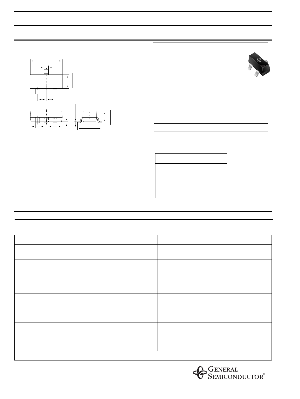
.122 (3.1)
.118 (3.0)
.016 (0.4)
3
12
.037(0.95)
.037(0.95)
.016 (0.4) .016 (0.4)
Dimensions in inches and (millimeters)
Pin configur ation
1 = Base, 2 = Emitter, 3 = Collector.
Top View
)
.056 (1.43
max. .004 (0.1)
)
.052 (1.33
.007 (0.175)
.005 (0.125)
.102 (2.6)
.094 (2.4)
.045 (1.15)
♦
PNP Silicon Epitaxial Planar Transistors
for switching, AF driver and amplifier
applications.
Especially suited for automatic insertion
♦
in thick- and thin-film circuits.
♦
These transistors are subdivided into three groups -16,
-25 and -40 according to their current gain.
♦
As complementary types, the NPN transistors BC817
and BC818 are recommended.
.037 (0.95)
MECHANICAL DATA
SOT-23 Plastic Package
Case:
FEATURES
Weight:
Marking code
approx. 0.008 g
Type Marking
BC807-16
-25
-40
BC808-16
-25
-40
5A
5B
5C
5E
5F
5G
Ratings at
Collector-Emitter Voltage BC807
Collector-Emitter Voltage BC807
Emitter-Base Voltage –V
Colle ctor Cu r rent –I
Peak Collector Current –I
Peak Base Current –I
Peak Emitter Current I
Power Dissipation at T
Junction Temperature T
Storage Temperature Range T
1)
Device on fiberglass substrate, see layout
ambient temperature unless otherwise specified
25 °C
= 50 °C P
SB
BC808
BC808
MAXIMUM RATINGS AND ELECTRICAL CHARACTERISTICS
Symbol Value Unit
–V
–V
–V
–V
EM
CES
CES
CEO
CEO
EBO
C
CM
BM
tot
j
S
50
30
45
25
V
V
V
V
5V
500 mA
1000 mA
200 mA
1000 mA
1)
310
mW
150 °C
–65 to +150 °C
4/98

Ratings at
ambient temperature unless otherwise specified
25 °C
DC Current Gain
at –V
at –V
= 1 V, –IC = 100 mA
CE
= 1 V, –IC = 300 mA -16
CE
BC807, BC808
ELECTRICAL CHARACTERISTICS
Current Gain Group-16
-25
-40
-25
-40
Symbol Min. Ty p. Max. Unit
h
FE
h
FE
h
FE
h
FE
h
FE
h
FE
100
160
250
60
100
170
–
–
–
–
–
–
250
400
600
–
–
–
–
–
–
–
–
–
Thermal Resistance Junction Substrate
Backside
Thermal Resistance Junction to Ambient Air R
Collector Saturation Voltage
at –I
= 500 mA, –IB = 50 mA
C
Base-Emitter Voltage
at –V
= 1 V, –IC = 300 mA
CE
Collector-Em i tter Cutoff Current
at –V
at –V
at –V
= 45 V BC807
CE
= 25 V BC808
CE
= 25 V, Tj = 150 °C
CE
Emitter-Base Cutoff Current
EB
= 4 V
at –V
Gain-Bandwidth Product
at –V
= 5 V, –IC = 10 mA, f = 50 MHz
CE
Collector-Base Capac itance
at –V
1)
= 10 V, f = 1 MHz
CB
Device on fiber glass sub st rate, see layout
.30 (7.5)
.12 (3)
R
–V
–V
–I
–I
–I
–I
f
T
C
thSB
thJA
CEsat
BE
CES
CES
CES
EBO
CBO
– – 320
– – 450
1)
1)
K/W
K/W
––0.7V
––1.2V
–
–
–
–
–
–
100
100
5
nA
nA
µA
– – 100 nA
– 100 – MHz
12 pF
.04 (1)
.08 (2)
.04 (1)
.59 (15 )
.03 (0.8)
.47 (12 )
0.2 (5)
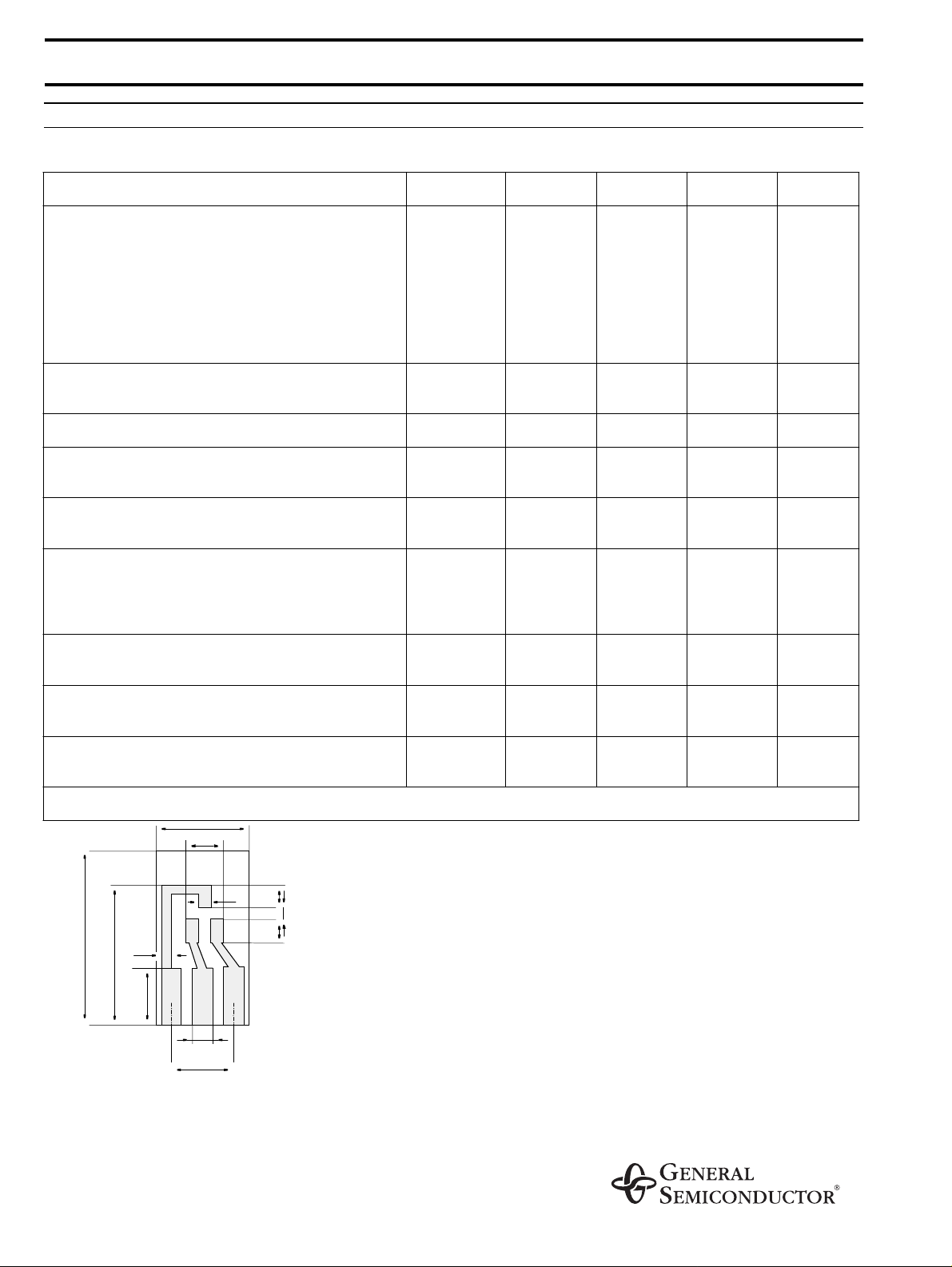
Layout for R
thJA
.06 (1.5)
.20 (5.1)
test
.08 ( 2)
Dimensions in inches (millimeters)
Thickness: Fiberglass 0.059 in (1.5 mm)
Copper leads 0.012 in (0.3 mm)
 Loading...