

Page 1

GE
Intelligent Platforms
Mini COM Express Type 10 Module
mCOM10-L1500
Hardware Reference Manual
GFK-2896
For public disclosure
Page 2

These instructions do not purport to cover all details or variations in equipment, nor to provide for every possible
contingency to be met during installation, operation, and maintenance. The information is supplied for informational
purposes only, and GE makes no warranty as to the accuracy of the information included herein. Changes, modifications,
and/or improvements to equipment and specifications are made periodically and these changes may or may not be reflected
herein. It is understood that GE may make changes, modifications, or improvements to the equipment referenced herein or to
the document itself at any time. This document is intended for trained personnel familiar with the GE products referenced
herein.
This document is approved for public disclosure.
GE may have patents or pending patent applications covering subject matter in this document. The furnishing of this
document does not provide any license whatsoever to any of these patents.
GE provides the following document and the information included therein as is and without warranty of any kind, expressed
or implied, including but not limited to any implied statutory warranty of merchantability or fitness for particular purpose.
For further assistance or technical information, contact the nearest GE Sales or Service Office, or an authorized GE Sales
Representative.
Issued: Aug 2014
Copyright © 2014 General Electric Company, All rights reserved.
___________________________________
* Indicates a trademark of General Electric Company and/or its subsidiaries.
All other trademarks are the property of their respective owners.
Refer to the section, Contact Information for support on this product.
Please send documentation comments or suggestions to controls.doc@ge.com
For public disclosure
Page 3

Acronyms and Abbreviations
ACPI Advanced Configuration and Power Interface
APIC Advanced Programmable Interrupt Controller
ATA ATAttachment
BIOS Basic Input/Output System
BIT Built-In Test
COM Computer on Module
CPU Central Processing Unit
DDR3 SDRAM Third-Generation Double Data Rate Synchronous Dynamic RAM
DMA Direct Memory Access
DIMM Dual In-line Memory Module
DP DisplayPort
DVI Digital Visual Interface
ECC Error Correcting Code
eDP Embedded DisplayPort
EEPROM Electrically-Erasable Programmable Read-Only Memory
EFI Extensible Firmware Interface
EHCI Enhanced Host Controller Interface
FPGA Field-Programmable Gate Array
FRU Field Replaceable Unit
GPIO General-Purpose Input/Output
GPU Graphics Processing Unit
HDMI High-Definition Multimedia Interface
2
I
C Inter-Integrated Circuit
IEEE Institute of Electrical and Electronic Engineers
JTAG Joint Test Access Group
LAN Local Area Network
LPC Low Pin-Count
LSB Least-Significant Byte
LVDS Low-Voltage Differential Signaling
MAC Media Access Control
MDI Media-Dependent Interface
MSB Most-Significant Byte
MSI Message-Signaled Interrupt
NMI Non-Maskable Interrupt
OS Operating System
PCI Peripheral Component Interconnect
PCIe PCI Express
PHY Physical
PIC Programmable Interrupt Controller
PICMG PCI Industrial Computer Manufacturers Group
PXE Preboot Execution Environment
RoHS Reduction of Hazardous Substances
RTC Real-Time Clock
SATA Serial ATA
SCI System Control Interrupt
Hardware Reference Manual GFK-2896 3
For public disclosure
Page 4

SIMD Single Instruction, Multiple Data
SKU Stock-keeping unit
SMBus System Management Bus
SMI System Management Interrupt
SPD Serial Presence Detect
SPI Serial Peripheral Interconnect
SR-IOV Single Root I/O Virtualization
TAP Test Access Port
TDP Thermal Design Power
TPM Trusted Platform Module
UART Universal Asynchronous Receiver/Transmitter
UDIMM Unbuffered DIMM
UEFI Unified EFI
UHCI Universal Host Controller Interface
USB Universal Serial Bus
VMDq Virtual Machine Device Queues
WDT WatchDog Timer
4 GFK-2896 Mini COM Express Type 10 Module mCOM10-L1500
For public disclosure
Page 5

Safety Symbol Legend
Indicates a procedure, condition, or statement that, if not
strictly observed, could result in personal injury or death.
Warning
Indicates a procedure, condition, or statement that, if not
strictly observed, could result in damage to or destruction of
equipment.
Caution
Indicates a procedure, condition, or statement that should be
strictly followed to improve these applications.
Attention
For public disclosure
Page 6

Support, Service, and Warranty
For support on the web and
product information, visit
our website at http://www.
ge-ip.com/.
This section provides information about our product warranty terms and details about what
action to take if you experience a problem with the product.
Warranty
The manufacturer grants the original purchaser of GE Intelligent Platforms products a warranty
of 24 months from the date of delivery. For details regarding this warranty, refer to the Terms
and Conditions of the initial sale.
Support
The GE Intelligent Platforms’ product support program features two regional support
headquarters and regional customer centers for support, service, RMA returns, and other
functions.
World-wide headquarters of GE Intelligent Platforms, Inc.
GE Intelligent Platforms Inc.
2500 Austin Drive
Charlottesville, VA 22911 U.S.A.
Regional Areas
WW world-wide
EU Europe, Russia, Near East, India, Africa
US Americas and Pacific Rim (Japan, Korea, China, Philippines, AUS, NZ)
Technical Support
Free technical support is available by phone or email. Telephone support is available at main
locations or at the regional center where the product was purchased.
Support Contact Information
Germany US
Monday through Thursday 8:00 – 17:00 (CET)
Friday 8:00 – 16:00 (CET)
Phone: +49-821-5034-170
Fax: +49-821-5034-119
Email: support.augsburg.ip@ge.com Email: support.embeddedsystems.ip@ge.com
Monday through Friday 8:30 AM – 5:30 PM (Eastern Time)
Phone: +1-800-322-3616
6 GFK-2896 Mini COM Express Type 10 Module mCOM10-L1500
For public disclosure
Page 7

Contents
1 Introduction ..................................................................................................................................... 11
1.1 Features ......................... ....................... ....................... ..................... .. .............................................. ... 12
2 Unpacking and Inspection ........................................................................................................... 15
2.1 Electrostatic Discharge ................... ....................... ....................... ....................... ................................... 15
2.2 Package Contents...................................... .............................................. .. ..................... ....................... . 16
2.3 Unpacking and Inspecting ........ .............................................. .. ..................... .......................................... 16
2.4 Handling......... .. .............................................. ..................... .............................................. .................. 17
3 Installation and Startup.................................................................................................................19
3.1 Required Materials............ .............................................. .............................................. ......................... 19
3.1.1 Carrier Board and Power Supply ....................................... .. ..................... .......................................... 19
3.1.2 Keyboard and Mouse .................. ....................... .............................................. ................................ 19
3.1.3 Video Monitor........... .............................................. .............................................. ..................... .... 19
3.2 General Installation Guidelines.................... .............................................. .. ..................... ....................... . 20
3.3 Installation Procedures................................... .............................................. ....................... .................... 21
3.3.1 Install the mCOM10-L1500 onto the Carrier Board ......................... .............................................. .. ...... 21
3.3.2 Install the Combined Unit .. .............................................. .. ............................................................... 22
3.4 Initial Startup................... ..................... .............................................. .............................................. .... 22
3.4.1 UEFI Firmware Setup ... .. .............................................. .............................................. ..................... 22
4 System Architecture ......................................................................................................................23
4.1 G-Series SoC Processor .... ..................... .. ............................................ .. .............................................. ... 23
4.1.1 Memory ... ....................... .............................................. .............................................. .................. 24
4.1.2 Digital Display Interface ....................................... .............................................. ..................... .. ...... 24
4.1.3 PCI Express ........................ .............................................. ..................... .. ...................................... 24
4.1.4 BIOS/UEFI Firmware ................................... ....................... .............................................. .............. 25
4.1.5 Serial ATA.................. .. ..................... .............................................. .............................................. 25
4.1.6 USB ... .............................................. .............................................. ..................... ......................... 25
4.1.7 Secure Digital or General-purpose I/O................................. .............................................. .................. 25
4.1.8 Audio ................................................................... .. ............................................ .. ..................... ... 25
4.1.9 Clocks .......... ..................... .............................................. .............................................. .. ............. 26
4.1.10 Real-Time Clock and CMOS RAM ................................. .............................................. ..................... 26
4.1.11 LPC Bus ....................................... .............................................. ..................... ............................. 26
4.1.12 SMBus............. .............................................. ....................... ....................... ....................... .......... 26
4.2 Gigabit Ethernet Interface .... .. ..................... .............................................. .............................................. 27
4.3 FPGA.................. .............................................. .............................................. ....................... ............. 28
4.3.1 Watchdog Timer ............... .............................................. .............................................. .................. 28
4.3.2 I
4.3.3 Serial Ports ............... .............................................. .............................................. ......................... 28
4.4 Power Distribution.................................... ....................... ....................... ..................... .. ........................ 29
4.4.1 Supervision and Reset .......... .. ..................... .............................................. ....................................... 29
4.4.2 Power Reset Sequence ................ ....................... .............................................. ................................ 29
4.4.3 Thermal Management ....... ..................... .. .............................................. .......................................... 29
4.5 Test and Debug ...................... ....................... ....................... ....................... .......................................... 30
4.6 Fan Monitor..................... ..................... .............................................. .............................................. .... 30
2
C Bus .................................. .............................................. ..................... .................................... 28
For public disclosure
GFK-2896 Hardware Reference Manual 7
Page 8

4.7 LED Status Indicators........................ .. ..................... .............................................. ................................ 30
5 Configuration................................................................................................................................... 31
5.1 Hardware ............................................. .............................................. .............................................. .... 31
5.1.1 COM Express Type 10 Module Connectors ................................. .............................................. ........... 31
5.1.2 JTAG Connector ...................... ................................................................... .................................... 40
5.1.3 PCIe Ports ............................. .............................................. .. ..................... ................................... 41
5.2 Software ....... ..................... .............................................. .............................................. .. .................... 42
5.2.1 Memory and I/O Address Mapping.................. .. ..................... .............................................. .............. 42
5.2.2 SMBus Slave Devices .......... .. ..................... .............................................. ....................................... 42
5.2.3 I
2
C Slave Devices ................... ....................... ....................... ....................... ................................... 42
5.2.4 External Interrupts.......... ....................... ....................... .............................................. ..................... 42
5.2.5 GPIO........................................ .............................................. ....................... ....................... ........ 43
6 FPGA Registers .............................................................................................................................. 45
6.1 Configuration Access Port ..................................... ..................... .............................................. .. ............. 45
6.1.1 Index Port. ....................... .............................................. .............................................. .................. 45
6.1.2 Data Port .................. .............................................. ..................... .............................................. .... 45
6.2 General Configuration Registers .................. .............................................. .. ..................... ....................... . 46
6.2.1 Logical Device Number ............................. ....................... ....................... ....................... ................. 46
6.2.2 Device ID ........................... ..................... .............................................. .. ..................... ................. 46
6.2.3 Version ............................................ .............................................. .. ..................... ....................... . 46
6.2.4 Revision....... .............................................. ....................... .............................................. .............. 47
6.2.5 Build Information .. .............................................. .............................................. ..................... .. ...... 47
6.3 UART Configuration Registers........................ .............................................. ..................... .. .................... 48
6.3.1 UART Control............................... .. ............................................ .. ..................... ............................ 48
6.3.2 UART Base Address............ .. ................................................................... ....................................... 48
6.3.3 UART Interrupt Request..................................... ..................... .............................................. ........... 49
6.3.4 UART Mode ......................................... ..................... .............................................. .. .................... 50
6.4 Supervision Configuration Registers....................................... ..................... .............................................. 51
6.4.1 Supervision Control............................ .............................................. .. ..................... ....................... . 51
6.4.2 Supervision Base Address......... ....................... ....................... ....................... ................................... 51
2
6.5 I
C Controller Configuration Registers.......................................... .............................................. .. ............. 52
2
6.5.1 I
6.5.2 I
6.5.3 I
6.6 Watchdog Timer Configuration Registers ................ ....................... .............................................. .............. 54
6.6.1 Watchdog Timer Control .............................................. ..................... .. ............................................ . 54
6.6.2 Watchdog Timer Base Address ........................... ..................... .. .............................................. .......... 54
6.6.3 Watchdog Timer IRQ.......................... .............................................. .. ..................... ....................... . 55
6.6.4 Watchdog Timer Options .................................................. .............................................. .................. 55
6.7 UART Run-Time Registers. .............................................. .............................................. ..................... .... 56
6.7.1 Receive Buffer ......................................... ....................... ....................... ....................... ................. 56
6.7.2 Transmit Buffer ............................................... ....................... ....................... ....................... .......... 56
6.7.3 Interrupt Enable ........ ....................... ....................... ..................... .. .............................................. ... 57
6.7.4 Interrupt Identification ................. ..................... .............................................. .. ............................... 58
6.7.5 FIFO Control ...................... ..................... .............................................. .. ...................................... 59
6.7.6 Line Control........................... ....................... ....................... ....................... ................................... 60
C Control ........... .............................................. ..................... .............................................. .. ...... 52
2
C Base Address ............. .............................................. .. .............................................. ................. 52
2
C IRQ..................................... .............................................. ..................... .. ............................... 53
8 GFK-2896 Mini COM Express Type 10 Module mCOM10-L1500
For public disclosure
Page 9

6.7.7 Modem Control .. ....................... ....................... .............................................. ................................ 61
6.7.8 Line Status........ .............................................. .............................................. .. ..................... .......... 62
6.7.9 Modem Status ...... .. ............................................ .. ..................... .............................................. ....... 63
6.7.10 Scratchpad................ .............................................. .............................................. ..................... .... 64
6.7.11 Divisor Latch ............................................... ..................... .............................................. .. ............. 64
6.8 Board Supervision Run-Time Registers..... ..................... .. .............................................. ............................ 65
6.8.1 Reset Cause .. .............................................. .. ..................... .............................................. .............. 65
6.8.2 Last Reset. ....................... .............................................. .............................................. .................. 66
2
6.9 I
C Controller Run-Time Registers.......................... .............................................. ....................... ............. 67
6.9.1 Clock Prescale........... .............................................. .............................................. ......................... 67
6.9.2 Control .................... ..................... .............................................. .............................................. .... 68
6.9.3 Transmit............................. .............................................. ....................... ....................... ............... 68
6.9.4 Receive....................... .............................................. ..................... .. ............................................ . 68
6.9.5 Command. .. .............................................. .............................................. ..................... .................. 69
6.9.6 Status . .............................................. .............................................. ..................... ......................... 70
6.9.7 Watchdog Timer Run-Time Registers.......... ....................... ....................... .......................................... 71
7 Specifications.................................................................................................................................. 73
Glossary of Terms ................................................................................................................................ 75
Index......................................................................................................................................................... 77
For public disclosure
GFK-2896 Hardware Reference Manual 9
Page 10

Notes
10 GFK-2896 Mini COM Express Type 10 Module mCOM10-L1500
For public disclosure
Page 11

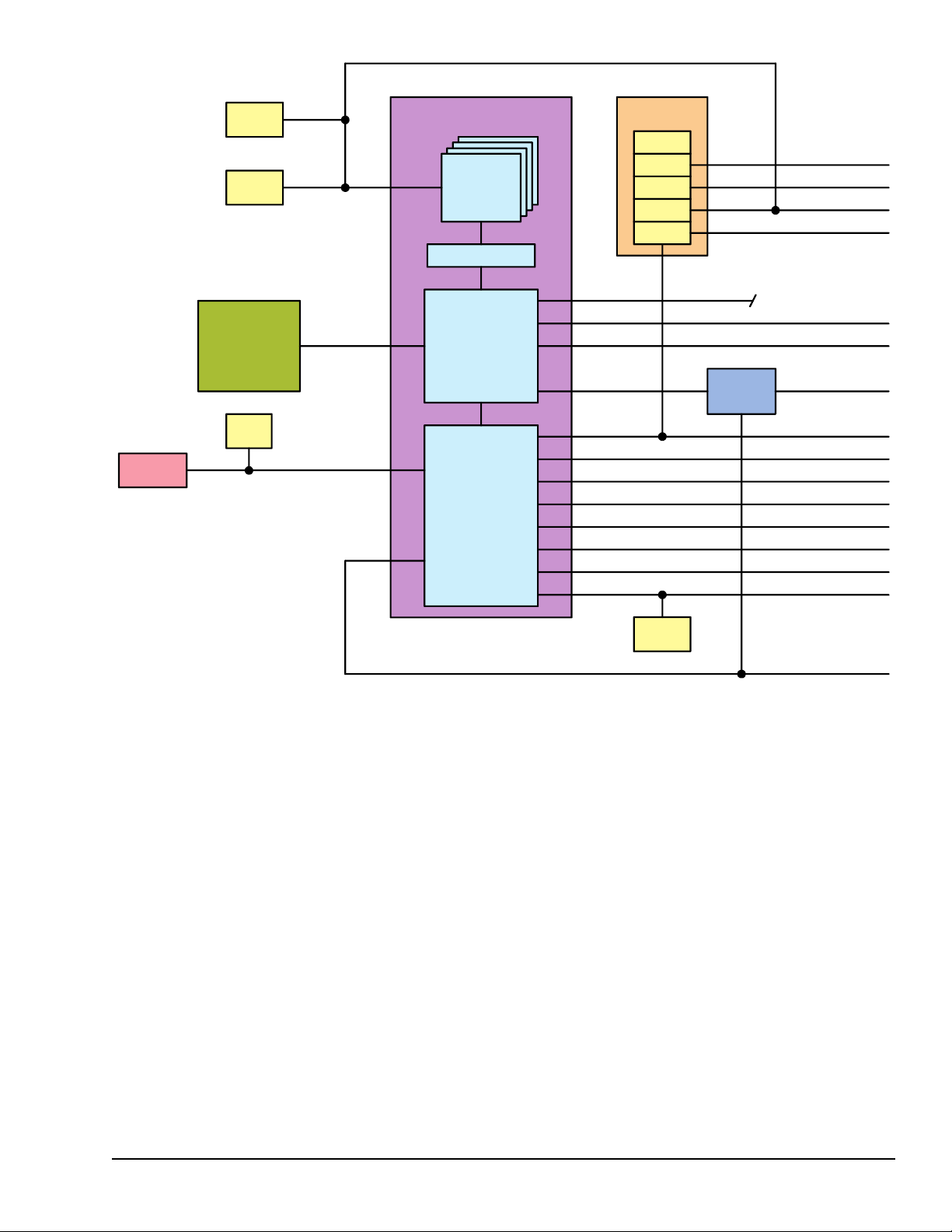
1 Introduction
The mCOM10-L1500 is a miniature Computer-on-Module (mCOM) Type 10
single-board computer approximately the size of a credit card, based on an AMD
G-Series System-on-chip (SoC). It contains one channel of DDR3L 72-bit ECC memory
and all components necessary for the bootable host computer packaged as a super
component. The mCOM10-L1500 module is combined with a carrier board required to
provide power, and support I/O and startup. The mCOM10-L1500 provides a Gigabit
Ethernet interface, four lanes of PCI Express (PCIe), two Serial ATA (SATA) ports, eight
USB 2.0 host interfaces (two of which support USB 3.0), low-voltage differential
signaling (LVDS) flat-panel or embedded DisplayPort plus a Digital Display Interface
(DDI), LPC, SPI, SMBus, I
audio ports to the module connector.
2
C, secure digital or general-purpose I/O, and high-definition
Refer to PICMG COM.0 R2.1
COM Express Module Base
Specification, located at
www.picmg.org.
This document describes the mCOM10-L1500 based on the PICMG COM Express
Module Base Specification. The module can operate in convection or conduction-cooled
environments, and uses a wide input-range main power rail (4.75 to 20 V), 5 V Standby,
and 3 V Real-Time Clock (RTC) battery power.
mCOM10-L1500
Introduction GFK-2896 Hardware Reference Manual 11
For public disclosure
Page 12

1.1 Features
The mCOM10-L1500 provides the following core hardware and firmware features:
• AMD G-Series SoC, including:
− Two or four CPU cores
− GPU core
− Northbridge
− DDR3 memory controller
− Integrated display output
− I/O controller
− Dual-core 9W TDP and quad-core 15W TDP SKUs available
• Single-channel 72-bit DDR3L SDRAM with ECC support: 2 GB, 4 GB, and 8 GB
options
• Gigabit Ethernet interface
• Four PCIe lanes, configurable as either 4×1 or 1×4
• Eight MB SPI Flash for UEFI/BIOS firmware
• Two SATA ports
• Eight USB 2.0 host interfaces, two of which also support USB 3.0 SuperSpeed
• Two simultaneous display outputs: LVDS/eDP (configurable), and DDI
• LPC Bus
• One internal plus one external SPI bus
• SMBus
2
• I
C bus
• SDIO or GPIO (configurable)
• High-definition Audio
• Two 16550-compatible serial ports
• Express Card support
• Power and system management
• Thermal protection
• 4.75 – 20 V primary power, 5 V Standby, and 3 V RTC power supply input
12 GFK-2896 Mini COM Express Type 10 Module mCOM10-L1500
For public disclosure
Page 13
G-Series SoC
CPU Core
L1 Cache
CPU Core
L1 Cache
CPU Core
L1 Cache
CPU Core
L1 Cache
L2 Cache
North Bridge
GPU
South Bridge
LVDS/eDP
DDI0
VGA
I210
PCIe
PCIe[0:3]
GbE0
DDR3L
2/4/8GB
ECC
2x SATA
8x USB
2x USB_SS
HDA
GPIO/SD
Flash
SMBus
LPC
FPGA
UART
I2C
WDog
UART
Supv
Ser0
Ser1
I2C
WDT
SPD
Debug
SPI
EeeP
SMBus
User
mCOM10-L1500 Functional Block Diagram
Introduction GFK-2896 Hardware Reference Manual 13
For public disclosure
Page 14

Notes
14 GFK-2896 Mini COM Express Type 10 Module mCOM10-L1500
For public disclosure
Page 15
2 Unpacking and Inspection
This chapter describes unpacking, initial inspection, and required preparation
considerations prior to using the mCOM10-L1500. Follow the procedures provided in this
chapter to verify proper operation after shipping and prior to system integration.
2.1 Electrostatic Discharge
Electrostatic Discharge (ESD), the discharge of static electricity, is a major cause of
electronic component failure. The module has been packed in a static-safe bag to protect
the board from ESD. Before removing the module or any other electronic product from its
static-safe bag, be prepared to handle it in a static-safe environment.
Static-sensitive devices; handle only at static safe work
stations.
Warning
This is an FCC Class A product for use in an industrial
environment. In a home or residential environment, this
product may cause radio interference in which case the
Caution
user may be required to take adequate measures.
Drain static electricity before you install or remove any
parts. Installing or removing modules without observing
this precaution could result in damage to this and/or
other modules in your system.
Caution
Wear a properly-functioning anti-static strap and make sure you are fully grounded. Any
surface upon which you place the unprotected module should be static-safe, which is
usually facilitated by the use of anti-static mats. From the time the board is removed from
the anti-static bag until it is in the card carrier and functioning properly, extreme care
should be taken to avoid zapping the board with ESD. Be aware that you could zap the
board without knowing it; a small discharge, imperceptible to the eye and touch, can often
be enough to damage electronic components. Extra caution should be taken in cold and
dry weather when electrostatics easily builds up.
Only after ensuring that both you and the surrounding area are protected from ESD,
carefully remove the board or module from the shipping carton by grasping the module
on its edges. Place the board, in its anti-static bag, flat down on a suitable surface. You
may then remove the board from the anti-static bag by tearing the ESD warning labels.
Unpacking and Inspection GFK-2896 Hardware Reference Manual 15
For public disclosure
Page 16
2.2 Package Contents
Verify that the delivered package contains one mCOM10-L1500 module.
2.3 Unpacking and Inspecting
Warning
Warning
Before installing or removing any board, ensure that
the system power and external supplies have been
turned off.
After unpacking the module, inspect it for visible
damage that could have occurred during shipping or
unpacking. If damage is observed (usually in the form
of bent component leads or loose socketed components),
contact GE Intelligent Platforms for additional
instructions. Depending on the severity of the damage,
it may be necessary to return the product to the factory
for repair.
DO NOT apply power to the board if it has visible
damage. Doing so may cause further, possibly
irreparable damage, as well as introduce a fire or shock
hazard.
Retain all packing material in case of future need.
Attention
Before unpacking the board or module, or fitting the device into your system, read the
manual carefully. Also adhere to the following guidelines:
• Observe all precautions for electrostatic sensitive modules
• If the product contains batteries, do not place the board on conductive surfaces,
anti-static plastic, or sponge, which can cause shocks and lead to battery or board
trace damage. Do not exceed the specified operational temperatures. Batteries and
storage devices might also have temperature restrictions.
• Keep all original packaging material for future storage or warranty shipments of the
board.
Although the module is carefully packaged to protect it against the rigors of shipping, it is
still possible that shipping damages may occur. Careful inspection of the shipping carton
should reveal some information about how the package was handled by the shipping
service. If evidence of damage or rough handling is found, notify the shipping service and
GE Intelligent Platforms as soon as possible.
16 GFK-2896 Mini COM Express Type 10 Module mCOM10-L1500
For public disclosure
Page 17

2.4 Handling
Proper handling of the board or module is critical to ensure proper operation and
long-term reliability. When unpacking and handling the board, be sure to hold the board
as displayed in the following figure.
Board Handling
Unpacking and Inspection GFK-2896 Hardware Reference Manual 17
For public disclosure
Page 18

Notes
18 GFK-2896 Mini COM Express Type 10 Module mCOM10-L1500
For public disclosure
Page 19

3 Installation and Startup
This chapter describes the installation of the mCOM10-L1500 module on a carrier board
and initial startup operations.
3.1 Required Materials
The following items are required to start the board in a standard configuration:
• Carrier board and power supply
• Keyboard and mouse
• Video monitor
3.1.1 Carrier Board and Power Supply
A carrier routes the I/O signals
of the mCOM10-L1500 to the
connectors.
Refer to chapter,
Specifications.
The keyboard is attached to the
carrier board.
You will need a carrier board wired with either an integrated or external regulated power
supply capable of providing stable low noise primary and standby sources. Verify that the
supply meets the voltage and total power requirements of the mCOM10-L1500.
Verify that the power supply is turned OFF while
plugging or unplugging the board onto or from a
carrier card, respectively.
Warning
3.1.2 Keyboard and Mouse
A compatible keyboard for initial system operation on the carrier board is required.
Depending on your application, this may be a standard keyboard, or one that uses
membrane switches for harsh environments.
3.1.3 Video Monitor
Any video monitor with an appropriate connection to a Digital Display Interface (DDI)
can be used initially for display output. Compatible interfaces are DisplayPort, DVI, and
HDMI. Access to the video signal is provided through the carrier board.
Installation and Startup GFK-2896 Hardware Reference Manual 19
For public disclosure
Page 20

3.2 General Installation Guidelines
Adhere to the following guidelines during installation:
• Observe all safety procedures to avoid damaging the system and protect operators
and users.
• Before installing or removing any board, verify that the system power and external
supplies have been turned off.
• Verify that the jumpers on the carrier board are correctly configured for your
application.
• Mount the board on the carrier board very carefully. Refer to the procedure, To install
the mCOM10-L1500 onto the carrier board.
• Do not restore power until all modules are fitted correctly and all connections have
been made properly.
20 GFK-2896 Mini COM Express Type 10 Module mCOM10-L1500
For public disclosure
Page 21

3.3 Installation Procedures
3.3.1 Install the mCOM10-L1500 onto the Carrier Board
A carrier board with a matching connector is required. Refer to the carrier board manual.
�� To install the mCOM10-L1500 onto the carrier board
1. Carefully slide the mCOM10-L1500 board onto the connector on the carrier board.
2. Fasten the mCOM10-L1500 to the board using four M2.5 screws. Tighten the screws
with a torque of 0.6 N-m (5 in-lb).
Installing the mCOM10-L1500 onto the Carrier Card
Installation and Startup GFK-2896 Hardware Reference Manual 21
For public disclosure
Page 22

3.3.2 Install the Combined Unit
�� To install the mCOM10-L1500 plus carrier board into a system
1. Before installing or removing any board, verify that the system power and external
2. Verify that the jumpers, if any, are correctly configured for your application.
3. Mount the unit very carefully.
4. Connect all I/O cables.
5. When all units are correctly fitted into the system and all connections have been
3.4 Initial Startup
A few seconds after powerup, the mCOM10-L1500 system UEFI Firmware banner
displays on the screen. If you do not see any error messages up to this point, the board is
running properly and ready to be installed and configured for your application.
3.4.1 UEFI Firmware Setup
Contact GE Intelligent
Platforms for technical
support. Refer to the section,
Support, Service, and
Warranty.
�� To enter setup during the initial startup sequence: press the Delete or F2
supplies have been turned off.
made properly, restore power.
during the boot up sequence. Adhere to the applicable on-screen messages when
prompted.
22 GFK-2896 Mini COM Express Type 10 Module mCOM10-L1500
For public disclosure
Page 23

4 System Architecture
This chapter describes the features, capabilities, and compatibilities of the mini COM
Express Type 10 module.
4.1 G-Series SoC Processor
The main component of the mCOM10-L1500 is the AMD G-Series SoC, which integrates
the following functions:
• Two or four processor cores
• Level1 and Level2 cache memory
• DDR3 memory controller
• Graphics processing unit (GPU)
• Support for two simultaneous displays on eDP or 18 bpp single-channel LVDS, or
DisplayPort 1.2, DVI, HDMI
• One ×4 PCI Express Gen2 link
• Four ×1 PCI Express Gen2 links
• Eight USB 2.0 host interfaces, two of which also support USB 3.0 SuperSpeed
• Two SATA 2.x/3.x controllers
• SD card reader 3.0 or SDIO controller
• LPC Bus interface
• High-definition audio
• General-purpose I/O
• SPI bus controller
• Two SMBus controllers
• Clock generator
The G-Series SoC uses the new generation Jaguar embedded processor from AMD that
offers the following features:
• Up to four execution cores
• 40-bit physical addressing, 48-bit virtual addressing
• 32-KB instruction and 32-KB L1 data caches per core
• 1-MB (dual-core) or 2-MB (quad-core) shared instruction/data L2 cache
Supported G-series SOC Models
Model Number Description
GX-209HA Dual-core, 9 W TDP, Industrial (-40 to 105°C, –40 to 221 °F T
GHz core clock
GX-411GA Quad-core, 15 W TDP, Industrial, 1.1 GHz core clock
J), 1.0
System Architecture GFK-2896 Hardware Reference Manual 23
For public disclosure
Page 24

4.1.1 Memory
The main memory array contains one channel of 72-bit wide DDR3L SDRAM, with
optional 2 GB, 4 GB, or 8 GB density. The system memory controller is integrated in the
G-Series SoC processor. A Serial Presence Detect (SPD) EEPROM, attached to the
internal SMBus, provides memory configuration information to the boot firmware.
Memory displays as a single-rank (2 or 4 GB) or dual-rank (8 GB) unbuffered DIMM.
The SPD chip also contains a temperature sensor physically located near the memory
array, allowing the refresh-time adjustments required for high-temperature operation.
Supported System Memory Options
Density Ranks Bus Width
2 GB 1 72 bit
4 GB 1 72 bit
8 GB 2 72 bit
4.1.2 Digital Display Interface
The mCOM10-L1500 supports two simultaneous video outputs with multiple modes. The
G-Series SoC integrates the new generation Radeon Sea Islands GPU, which supports
DirectX 11.1. There is no independent memory dedicated to the GPU video frame buffer
so a portion of main memory must be reserved for this purpose. Two digital video outputs
are provided. Analog video is not used.
Video Outputs
Video Output
DP0 LVDS or Embedded DisplayPort Wired to COMe LVDS/eDP connector pins
DP1 DVI, HDMI, or DisplayPort Wired to COMe DDI0 connector pins
Description
Configuration
4.1.3 PCI Express
The G-Series SoC hosts two PCI Express (PCIe) root complex ports. Four ×1
general-purpose PCIe lanes are wired to the COM Express connector, and support Gen1
(2.5 Gbps) and Gen2 (5 Gbps) speeds. One lane of a ×4 PCIe port is wired to an on-board
Ethernet controller, while the remaining three lanes are unused.
24 GFK-2896 Mini COM Express Type 10 Module mCOM10-L1500
For public disclosure
Page 25

4.1.4 BIOS/UEFI Firmware
Refer to PICMG COM.0 R2.1
COM Express Module Base
Specification located at
www.picmg.org.
BIOS
DIS1#
1 1 Module Module High Module SPI0/SPI1
1 0 Module Module High Module Carrier FWH (LPC)
0 1 Module Carrier SPIO Carrier SPI0/SPI1
0 0 Carrier Module SPI1 Module SPI0/SPI1
BIOS DIS0# Chipset SPI_
CS1#
The mCOM10-L1500 has an on-board 8 MByte SPI Flash ROM device that holds the
BIOS/UEFI firmware load. Alternatively, the module may be configured to boot from the
Flash located on the carrier board, on either the external SPI bus or LPC bus. This is
controlled by the carrier board using the BIOS_DIS[0:1]# straps.
UEFI Load
Chipset SPI_
CS0#
Carrier SPI_
CS#
SPI_
Descriptor
BIOS Entry
4.1.5 Serial ATA
Two Serial ATA (SATA) controllers, integrated into the G-Series SoC, host mass storage
units on the carrier through the COM Express connector. SATA 2.x (3 Gbps) and 3.x (6
Gbps) are supported. A combined SATA activity indicator is also provided.
4.1.6 USB
The mCOM10-L1500 provides eight G-Series SoC USB controllers to host serial links
through the COM Express connector. All ports support USB 2.0, while ports 8 and 9 also
support USB 3.0 SuperSpeed. The following table provides port mapping between the
G-Series SoC and the COM Express connector.
USB Port Assignments
Port USB Interface
0 Unused N/A
1 Unused N/A
2 mCOMe USB 2
3 mCOMe USB 3
4 mCOMe USB 4
5 mCOMe USB 5
6 mCOMe USB 6
7 mCOMe USB 7
8 mCOMe USB 0
9 mCOMe USB 1
Speed
FS, HS
FS, HS
FS, HS
FS, HS
FS, HS
FS, HS
FS, HS, SS
FS, HS, SS
4.1.7 Secure Digital or General-purpose I/O
The G-Series SoC provides a Secure Digital (SD) 3.0 compliant host controller wired
directly to the COM Express connector. Alternatively, these pins may be used as simple
general-purpose input/output (four pins each).
4.1.8 Audio
The G-Series SoC provides a basic PC speaker output, as well as a High Definition Audio
(HDA) controller wired to the COM Express connector.
System Architecture GFK-2896 Hardware Reference Manual 25
For public disclosure
Page 26

4.1.9 Clocks
Most of the system clocks are generated from a 48 MHz crystal by an integrated clock
generator within the G-Series SoC. The following clock groups are provided by the clock
generator:
Internal clocks are supplied to the CPU cores, cache, GPU, peripheral controllers, and
the intra-chip buses.
A 25 MHz crystal provides the
clock required by the Ethernet
controller, PHY.
The RTC oscillator uses a
32.768 kHz crystal.
Memory clock is supplied to the DDR3L memory as 533, 667, or 800 MHz, depending
on memory configuration.
100 MHz Differential PCIe Reference clock is supplied to the Ethernet controller,
and to the carrier board.
33.33 MHz LPC clock is supplied to the FPGA LPC interface, and to the carrier board.
Note The power sequencing and startup supervision logic in the FPGA is clocked with a
separate 25 MHz oscillator powered on the standby rail prior to the main clock generator
starting.
4.1.10 Real-Time Clock and CMOS RAM
The G-Series SoC provides the real-time clock (RTC) and CMOS RAM functions. This is
powered from the VCC_RTC pin, and must be supplied by the carrier prior to ramp up of
the standby and main power rails for proper board operation. Battery back-up, if required,
must also be implemented on the carrier board.
4.1.11 LPC Bus
A standard low pin-count bus, including serial interrupt request, is hosted by the G-Series
SoC, and connects to on-board peripherals within an FPGA and to the COM Express
connector. The bus operates at 33.33 MHz.
4.1.12 SMBus
The mCOM10-L1500 contains two system management buses (SMBus): SMB0 and
SMB1. Both are controlled by the G-Series SoC. SMB0 connects to the memory SPD and
the debug header, and is located on the S0 (main) power domain. SMB1 connects to the
Ethernet controller and the COM Express connector, and is located on the S5 (standby)
power domain.
26 GFK-2896 Mini COM Express Type 10 Module mCOM10-L1500
For public disclosure
Page 27

4.2 Gigabit Ethernet Interface
The mCOM10-L1500 provides one 10/100/1000 Mbps MDI through an Intel I210
Gigabit Ethernet Controller. The I210 controller supports the following features:
• Jumbo frames up to 9.5 KB
• 802.1q VLAN
• 64-bit addressing
• IEEE 1588 time synchronization (per-packet timestamp)
The I210 MDI port is wired directly to the COM Express connector. Isolation should be
implemented on the carrier board. Three status LED outputs from the I210 are decoded in
the FPGA to produce four Ethernet link and activity indicators connected to the COM
Express connector.
Note An attached 512-KB serial Flash is provided for the I210 to store Ethernet
configuration data, such as the MAC address, along with optional ROM modules, such as
a PXE driver or UEFI network driver.
System Architecture GFK-2896 Hardware Reference Manual 27
For public disclosure
Page 28

4.3 FPGA
Refer to Chapter, FPGA
Registers.
Reloading the watchdog timer
involves a register unlock
sequence, followed by setting
the reload bit.
The on-board I2C bus is also
connected to the G-Series SoC
Sideband Temperature Sensor
Interface (SB-TSI), which
provides local and remote
temperature monitoring of the
CPU.
The mCOM10-L1500 includes an FPGA that provides board supervision with control of
the powerup, power down, and reset sequencing. It also contains the watchdog timer, I²C
controller, and two UARTS. System interface is provided through the LPC bus.
4.3.1 Watchdog Timer
The FPGA provides a dedicated two-stage watchdog timer (WDT) for the
mCOM10-L1500 processor that checks for non-recoverable software errors/loops. Each
stage has an independent count-down value ranging from 8 µsec to about 134.2 seconds
(using a 125-kHz prescale clock). Timeout of the first stage generates an interrupt request
to the processor and arms the second stage. Timeout of the second stage asserts the WDT
pin, and may also generate a non-maskable interrupt or reset the processor. The watchdog
timer is disabled on startup and after board reset. It is enabled and disabled using a
configuration register bit, and can be locked to prevent spurious or unintentional changes.
Once locked, it remains locked until reset.
4.3.2 I2C Bus
A standard I2C bus is wired to the COM Express connector. The FPGA provides the I2C
controller as an LPC-bus peripheral. The I
store module-specific data. The bus operates on standby power, and is compatible with
multi-master operation. This allows the EEPROM to be read by the carrier board prior to
powering up the module.
4.3.2.1 Non-Volatile Memory
2
C bus is wired to a 4 KB EEPROM used to
The mCOM10-L1500 contains a 4 KB serial EEPROM located on the I2C bus for storage
of non-volatile module-specific information. An additional 4 KB EEPROM is provided
for general-purpose non-volatile user data, such as O/S boot parameters.
4.3.3 Serial Ports
The FPGA implements two 16550-compatible UARTs that provide standard serial
communication ports, supporting data rates up to 230.4 kbps. Only transmit and receive
data are wired to the COM Express connector, as there are no pins defined for the modem
and line control signals.
28 GFK-2896 Mini COM Express Type 10 Module mCOM10-L1500
For public disclosure
Page 29

4.4 Power Distribution
The mCOM10-L1500 module draws all required load current from the carrier board
through the COM Express connector. There are three power sources:
• RTC (VCC_RTC)
• Standby (VCC_5V_SBY)
• Primary (VCC_12V)
RTC battery power is required and must be stable prior to the application of standby or
primary power. Standby power is optional, but must be supplied if standby operation is
required, such as S3 suspend-to-RAM state. The mCOM10-L1500 is compatible with
wide input range (4.75 to 20 V) primary power, as defined in the PICMG COM.0, R2.1
specification for mini modules. Internally, the standby and primary inputs are diode
OR-ed to form an auxiliary power rail (VIN_AUX), which is used to supply the memory
and other standby circuits.
4.4.1 Supervision and Reset
The Supervision module is responsible for all payload power sequencing and device reset
control. Hard reset sources include startup, overtemperature, watchdog timeout, system
reset from the carrier, and debug header.
4.4.2 Power Reset Sequence
VCC_RTC must be present for a minimum of five seconds prior to the application of
standby or primary power to ensure proper board operation. This will not be an issue for
battery-backed systems other than the initial battery installation. For battery-less systems,
the carrier board must hold off standby and primary power to meet the five second
requirement when the system powers up. Once VCC_5V_SBY or VCC_12V is applied, the
on-board standby supplies will power up and the module enters the S5 state.
To move from standby to active state, primary power, (VCC_12V) must be applied and
stable with PWR_OK as True, and the power button signal (PWRBTN#) must be asserted.
Once SUS_S5# goes high, the memory supply is enabled. The on-board main supplies
will then power up in sequence. Once all power supplies have started and are stable, CB_
RESET# is released by the module approximately 120 ms later.
4.4.3 Thermal Management
Temperature behavior of the board is influenced by two thermal zones for CPU and
memory. Each zone consists of two thresholds, T(HOT) and T(CRIT). If the hot threshold
is reached, an ACPI-aware operating system (such as Microsoft
shutdown to S4 with no data loss. If the critical threshold is reached, an emergency
shutdown to S5 is forced immediately. Non-ACPI aware operating systems (such as DOS
or VxWorks) only provide an emergency shutdown to S5 when the critical threshold is
reached. Overheating of the carrier can be signaled to the module by asserting #THRM. A
high to low edge is detected by the embedded controller, and an ACPI event is sent to the
operating system.
©
Windows) forces a
System Architecture GFK-2896 Hardware Reference Manual 29
For public disclosure
Page 30

4.5 Test and Debug
APU_Sel#
Board_Sel#
G-Series
SoC
I210FPGA
JTAG
Connector
The mCOM10-L1500 module provides JTAG access for the compatible ICs on the
following:
• G-Series SoC
• FPGA
• I210 Ethernet controller
JTAG is used for multiple purposes (FPGA programming, board testing, and processor
debugging), and the devices reside on different power domains (standby/auxiliary for the
FPGA and I210 Ethernet controller, and primary for the SoC). Therefore, the chain is
segmented so that only the appropriate devices are included. A 23-pin flex-cable
receptacle is provided to access the board’s JTAG chain, and for controlling its
configuration, based on two select lines. With Board_Sel# alone asserted, only the FPGA
and I210 are included in the chain, which facilitates programming of the FPGA. For
processor debug, APU_Sel# alone is asserted, and the G-Series SoC will be the only
device in the chain.
JTAG Chain Connections
4.6 Fan Monitor
The CPU temperature is monitored and compared with a target temperature. A PID
controller sets the fan speed output on FAN_PWMOUT accordingly. The appropriate fan
driver circuit must be implemented at the carrier. Target temperature and PID control
values may be configured during UEFI setup.
4.7 LED Status Indicators
There is a single green status LED on the mCOM10-L1500 module. It will be off until
power is applied and code execution starts, will blink during UEFI initialization, and then
become solid when initialization is complete shortly before operating system restart.
30 GFK-2896 Mini COM Express Type 10 Module mCOM10-L1500
For public disclosure
Page 31

5 Configuration
There are no user-configurable
hardware options on the
mCOM10-L1500.
5.1 Hardware
Refer to the procedure, To
install the mCOM10-L1500
onto the carrier board.
Pin #
A1 GND B1 GND
A2
A3
A4
A5
A6
A7
A8
A9
A10
A11 GND B11 GND
A12
A13
A14
A15
A16
A17
A18
A19
A20
A21 GND B21 GND
A22
A23
A24
A25
A26
A27 BATLOW# B27 WDT
A28
A29
The mCOM10-L1500 has been thoroughly tested, and is ready for use in your system. To
verify mCOM10-L1500 operation for the first time, only configure a minimal system. It is
not necessary to have disk drives, a Flash disk, or other accessories connected to perform
the mCOM10-L1500 UEFI boot sequence.
5.1.1 COM Express Type 10 Module Connectors
The COM Express connectors are used to interface the mCOM10-L1500 to the carrier
board. Connect the COM Express receptacle, located on the solder side of the module, to
the COM Express plug on the carrier board.
mCOM10-L1500 Connector Pin Assignments
Signal
GBE0_MDI3–
GBE0_MDI3+
GBE0_LINK100#
GBE0_LINK1000#
GBE0_MDI2–
GBE0_MDI2+
GBE0_LINK#
GBE0_MDI1–
GBE0_MDI1+
GBE0_MDI0–
GBE0_MDI0+
GBE0_CTREF
SUS_S3#
SATA0_TX+
SATA0_TX–
SUS_S4#
SATA0_RX+
SATA0_RX–
USB_SSRX0–
USB_SSRX0+
SUS_S5#
USB_SSRX1–
USB_SSRX1+
SATA_ACT#
AC/HDA_SYNC
Pin #
B2
B3
B4
B5
B6
B7
B8
B9
B10
B12 PWRBTN#
B13
B14
B15
B16
B17
B18
B19
B20
B22
B23
B24
B25
B26
B28
B29
Signal
GBE0_ACT#
LPC_FRAME#
LPC_AD0
LPC_AD1
LPC_AD2
LPC_AD3
LPC_DRQ0#
LPC_DRQ1#
LPC_CLK
SMB_CK
SMB_DAT
SMB_ALERT#
SATA1_TX+
SATA1_TX–
SUS_STAT#
SATA1_RX+
SATA1_RX–
USB_SSTX0–
USB_SSTX0+
PWR_OK
USB_SSTX1–
USB_SSTX1+
AC/HDA_SDIN2
AC/HDA_SDIN1
Configuration GFK-2896 Hardware Reference Manual 31
For public disclosure
Page 32

Pin #
A30
A31 GND B31 GND
A32
A33
A34
A35 THRMTRIP# B35 THRM#
A36 USB6– B36 USB7–
A37 USB6+ B37 USB7+
A38
A39 USB4– B39 USB5–
A40 USB4+ B40 USB5+
A41 GND B41 GND
A42 USB2– B42 USB3–
A43 USB2+ B43 USB3+
A44
A45 USB0– B45 USB1–
A46 USB0+ B46 USB1+
A47
A48
A49
A50
A51 GND B51 GND
A52 RSVD B52 RSVD
A53 RSVD B53 RSVD
A54 GPI0 B54 GPO1
A55 RSVD B55 RSVD
A56 RSVD B56 RSVD
A57 GND B57 GPO2
A58
A59
A60 GND B60 GND
A61
A62
A63 GPI1 B63 GPO3
A64
A65
A66 GND B66 WAKE0#
A67 GPI2 B67 WAKE1#
A68
A69
A70 GND B70 GND
A71
A72
A73
A74
A75
A76
A77
A78
Signal
AC/HDA_RST#
AC/HDA_BITCLK
AC/HDA_SDOUT
BIOS_DIS0#
USB_6_7_OC#
USB_2_3_OC#
VCC_RTC
EXCD0_PERST#
EXCD0_CPPE#
LPC_SERIRQ
PCIE_TX3+
PCIE_TX3–
PCIE_TX2+
PCIE_TX2–
PCIE_TX1+
PCIE_TX1–
PCIE_TX0+
PCIE_TX0–
LVDS_A0+
LVDS_A0–
LVDS_A1+
LVDS_A1–
LVDS_A2+
LVDS_A2–
LVDS_VDD_EN
LVDS_A3+
Pin #
B30
B32 SPKR
B33
B34
B38
B44
B47
B48
B49
B50
B58
B59
B61
B62
B64
B65
B68
B69
B71
B72
B73
B74
B75
B76
B77
B78
Signal
AC/HDA_SDIN0
I2C_CK
I2C_DAT
USB_4_5_OC#
USB_0_1_OC#
EXCD1_PERST#
EXCD1_CPPE#
SYS_RESET#
CB_RESET#
PCIE_RX3+
PCIE_RX3–
PCIE_RX2+
PCIE_RX2–
PCIE_RX1+
PCIE_RX1–
PCIE_RX0+
PCIE_RX0–
DDI0_PAIR0+
DDI0_PAIR0–
DDI0_PAIR1+
DDI0_PAIR1–
DDI0_PAIR2+
DDI0_PAIR2–
DDI0_PAIR4+
DDI0_PAIR4–
32 GFK-2896 Mini COM Express Type 10 Module mCOM10-L1500
For public disclosure
Page 33

Pin #
A79
A80 GND B80 GND
A81
A82
A83
A84
A85 GPI3 B85
A86 RSVD B86
A87
A88
A89
A90 GND B90 GND
A91
A92
A93 GPO0 B93
A94
A95
A96
A97 TYPE10# B97
A98
A99
A100 GND B100 GND
A101
A102
A103 LID# B103 SLEEP#
A104
A105
A106
A107
A108
A109
A110 GND B110 GND
Signal
LVDS_A3–
LVDS_A_CK+
LVDS_A_CK–
LVDS_I2C_CK
LVDS_I2C_DAT
eDP_HPD
PCIE_CLK_REF+
PCIE_CLK_REF–
SPI_POWER
SPI_MISO
SPI_CLK
SPI_MOSI
TPM_PP
SER0_TX
SER0_RX
SER1_TX
SER1_RX
VCC_12V
VCC_12V
VCC_12V
VCC_12V
VCC_12V
VCC_12V
Pin #
B79
B81
B82
B83
B84
B87
B88
B89
B91
B92
B94
B95
B96
B98
B99
B101
B102
B104
B105
B106
B107
B108
B109
Signal
LVDS_BKLT_EN
DDI0_PAIR3+
DDI0_PAIR3–
LVDS_BKLT_CTRL
VCC_5V_SBY
VCC_5V_SBY
VCC_5V_SBY
VCC_5V_SBY
BIOS_DIS1#
DDI0_HPD
DDI0_PAIR5+
DDI0_PAIR5–
DDI0_PAIR6+
DDI0_PAIR6–
DDI0_DDC_AUX_SEL
USB_HOST_PRSNT
SPI_CS#
DDI0_CTRLCLK_AUX+
DDI0_CTRLDATA_AUX–
FAN_PWMOUT
FAN_TACHIN
VCC_12V
VCC_12V
VCC_12V
VCC_12V
VCC_12V
VCC_12V
Configuration GFK-2896 Hardware Reference Manual 33
For public disclosure
Page 34

5.1.1.1 Signal Descriptions
HDA Interface
Signal
HDA_RST# O
HDA_SYNC O
HDA_BITCLK I/O
HDA_SDOUT O
HDA_SDIN[0:2] I/O
Signal
GBE0_MDI[0:3]± I/O
GBE0_ACT# OD
GBE0_LINK# OD
GBE0_LINK100# OD
GBE0_LINK1000# OD
GBE0_CTREF REF N/A Ethernet magnetics center tap reference. Floating.
Pin Type
CMOS
CMOS
CMOS
CMOS
CMOS
Pin Type
ETH
CMOS
CMOS
CMOS
CMOS
Voltage Supply
3.3 V Suspend
3.3 V
3.3 V
3.3 V
3.3 V
3.3 V
3.3 V
3.3 V
3.3 V
3.3 V
Ethernet
Voltage Supply
3.3 V Suspend
3.3 V
3.3 V Suspend
3.3 V
3.3 V Suspend
3.3 V
3.3 V Suspend
3.3 V
3.3 V
3.3 V
Description
Reset output to CODEC
Sample synchronization signal to CODEC
Serial data clock generated by external CODEC
Serial TDM data to the CODEC
Serial TDM data inputs from up to three CODECs
Description
Media Dependent Interface differential pairs 0-3
Activity indicator
Link indicator
100 Mbps link indicator
1000 Mbps (1 Gbps) link indicator
Signal
SATA0_TX± O
SATA0_RX± I
SATA1_TX± O
SATA1_RX± I
SATA_ACT# OD
Signal
PCIE_TX[0:3]± O
PCIE_RX[0:3]± I
PCIE_CLK_REF± O
Pin Type
SATA
SATA
SATA
SATA
CMOS
Pin Type
PCIE
PCIE
PCIE
SATA
Voltage Supply
AC coupled on module Channel 0 transmit differential pair transmit signals
AC coupled on module Channel 0 receive differential pair receive signals
AC coupled on module Channel 1 transmit differential pair transmit signals
AC coupled on module Channel 1 receive differential pair receive signals
3.3 V
3.3 V
General-purpose PCIe Lanes
Voltage Supply
AC coupled on module PCI Express differential Transmit pairs 0-3
AC coupled on carrier
board
N/A PCI Express differential reference Clock 100 MHz
Description
Activity indicator
Description
PCI Express differential receive pairs 0-3
34 GFK-2896 Mini COM Express Type 10 Module mCOM10-L1500
For public disclosure
Page 35

PCIe Board
Signal
EXCD[0:1]_CPPE# I
EXCD[0:1]
_PERST#
Signal
USB[0:7]± I/O
USB_0_1_OC# I
USB_2_3_OC# I
USB_4_5_OC# I
USB_6_7_OC# I
USB_SSTX[0:1]± I/O AC coupled on module Additional transmit differential pairs for SuperSpeed
USB_SSRX[0:1]± I/O AC coupled on carrier
USB_HOST_
PRSNT
Pin Type
CMOS
O
CMOS
Pin Type
USB
CMOS
CMOS
CMOS
CMOS
N/A N/A USB host present on the carrier indicator. Not used.
Voltage Supply
3.3 V
3.3 V
3.3 V
3.3 V
USB
Voltage Supply
3.3 V suspend
3.3 V
3.3 V suspend
3.3 V
3.3 V suspend
3.3 V
3.3 V suspend
3.3 V
3.3 V suspend
3.3 V
board
Description
PCI Express capable board request
PCI Express Board reset
Description
USB channels 0-7 differential pairs
Overcurrent sense, channels 0 and 1
Overcurrent sense, channels 2 and 3
Overcurrent sense, channels 4 and 5
Overcurrent sense, channels 6 and 7
USB data
Additional receive differential pairs for SuperSpeed
USB data
Signal
LVDS_A[0:2]± O
LVDS_A[3]± O
LVDS_A_CK± O
LVDS_VDD_EN O
LVDS_BKLT_EN O
LVDS_BKLT_CTRL O
LVDS_I2C_CK I/O OD
LVDS_I2C_DAT I/O OD
eDP_HPD 3.3 V
Pin Type
LVDS
LVDS
CMOS
CMOS
CMOS
CMOS
CMOS
CMOS
Voltage Supply
LVDS LVDS or eDP differential pairs 0-2
LVDS LVDS differential pair 3. Unused for eDP.
3.3 V
3.3 V
3.3 V
3.3 V
3.3 V
3.3 V
3.3 V
3.3 V
3.3 V
3.3 V
3.3 V
3.3 V
3.3 V
LVDS/eDP
Description
LVDS clock or eDP differential pair 3
LVDS panel or eDP power enable
LVDS panel or eDP backlight enable
LVDS panel or eDP backlight brightness control
LVDS I2C clock or eDP AUX+
LVDS I2C data line or eDP AUX–
Detection of hot plug/unplug for eDP. Unused for
LVDS.
Configuration GFK-2896 Hardware Reference Manual 35
For public disclosure
Page 36

Signal
LPC_AD[0:3] I/O
LPC_FRAME# O
LPC_DRQ[0:1]# I
LPC_SERIRQ I/O
LPC_CLK O
Signal
SPI_CS# O
SPI_MISO I
SPI_MOSI O
SPI_CLK O
SPI_POWER O
BIOS_DIS[0:1]# I
Pin Type
CMOS
CMOS
CMOS
CMOS
CMOS
Pin Type
CMOS
CMOS
CMOS
CMOS
CMOS
CMOS
LPC Bus
Voltage Supply
3.3 V
3.3 V
3.3 V
3.3 V
3.3 V
3.3 V
3.3 V
3.3 V
3.3 V
3.3 V
SPI Bus
Voltage Supply
3.3 V
3.3 V
3.3 V
3.3 V
3.3 V
3.3 V
3.3 V
3.3 V
3.3 V suspend
3.3 V
3.3 V
3.3 V
Description
Multiplexed address, command, and data bus
Frame start of cycle indicator
Serial DMA request. LPC_DRQ1# is not supported.
Serial interrupt request
33.33 MHz bus clock
Description
Chip select for carrier board devices
Master-in/slave-out data to module from carrier
Master-out/slave-in data from module to carrier
Bus clock
Power supply for carrier board SPI. Connected to
+3.3 V standby supply
BIOS boot device selection straps
Signal
DDI0_PAIR[0:3]± O
DDI0_PAIR[4:6]± I
DDI0_DDC_AUX_
SEL
DDI0_CTRLCLK_
AUX+
DDI0_CTRLDATA_
AUX–
DDI0_HPD I
Pin Type
PCIE
CMOS
I/O
PCIE
I/O OD
CMOS
I/O
PCIE
I/O OD
CMOS
I/O
PCIE
I/O OD
CMOS
CMOS
DDI
Voltage Supply
AC coupled on module Differential pairs 0-3
3.3 V
3.3 V
AC coupled on module
3.3 V
AC coupled on module
3.3 V
AC coupled on module
3.3 V
3.3 V
3.3 V
Description
Differential pairs 4-6. Not connected.
DDC or AUX function select
DP AUX+ or DDC clock
DP AUX– or DDC data
Hot-plug detect
36 GFK-2896 Mini COM Express Type 10 Module mCOM10-L1500
For public disclosure
Page 37

Serial Interfaces
Signal
SER[0:1]_TX O
SER[0:1]_RX I
Signal
I2C_CK I/O
I2C_DAT I/O
Signal
SPKR O
WDT O
FAN_PWMOUT O 3.3 V
FAN_TACHIN I 3.3 V
TPM_PP NC N/A Trusted platform module physical presence. Not
Pin Type
CMOS
CMOS
Pin Type
CMOS
CMOS
Pin Type
CMOS
CMOS
Voltage Supply
3.3 V
12 V
3.3 V
12 V
2
I
C Bus
Voltage Supply
3.3 V
3.3 V
3.3 V suspend
3.3 V
Miscellaneous
Voltage Supply
3.3 V
3.3 V
3.3 V
3.3 V
3.3 V
3.3 V
Description
General-purpose serial port 0-1 transmitter
General-purpose serial port 0-1 receiver
Description
Serial clock
Serial data
Description
Audio output to speaker
Watchdog time-out event indication
Fan pulse-width modulation speed control
Fan tachometer reading
connected.
Power and System Management
Signal
PWRBTN# I
SYS_RESET# I
CB_RESET# O
PWR_OK IO
SUS_STAT# I
SUS_S3# O
SUS_S4# O
SUS_S5# O
WAKE0# I
WAKE1# I
BATLOW# I
LID# NC N/A LID switch
SLEEP# NC N/A Sleep button
Pin Type
CMOS
CMOS
CMOS
CMOS
CMOS
CMOS
CMOS
CMOS
CMOS
CMOS
CMOS
Voltage Supply
3.3 V Suspend
3.3 V
3.3 V Suspend
3.3 V
3.3 V Suspend
3.3 V
3.3 V
3.3 V
3.3 V Suspend
3.3 V
3.3 V Suspend
3.3 V
3.3 V Suspend
3.3 V
3.3 V Suspend
3.3 V
3.3 V Suspend
3.3 V
3.3 V
3.3 V
3.3 V Suspend
3.3 V
Description
Power button
System reset
Carrier board reset
Main power OK
Suspend status
Suspend-to-RAM state indication
Suspend-to-disk state indication
Soft off state indication
PCI Express wake-up signal
General-purpose wake-up signal
External battery low indication
Configuration GFK-2896 Hardware Reference Manual 37
For public disclosure
Page 38

Signal
THRM# I
THRMTRIP# O
Signal
SMB_CK I/O OD
SMB_DAT I/O OD
SMB_ALERT# I
Signal
GPI0 I
GPI1 I/O
GPI2 O
GPI3 O
GPO0 O
GPO1 O
GPO2 I
GPO3 I
Pin Type
CMOS
CMOS
Pin Type
CMOS
CMOS
CMOS
Pin Type
CMOS
CMOS
CMOS
CMOS
CMOS
CMOS
CMOS
CMOS
Thermal Protection
Voltage Supply
3.3 V suspend
3.3 V
3.3 V
3.3 V
Voltage Supply
3.3 V suspend
3.3 V
3.3 V suspend
3.3 V
3.3 V suspend
3.3 V
General-Purpose or SD I/O
Voltage Supply
3.3 V
3.3 V
3.3 V
3.3 V
3.3 V
3.3 V
3.3 V
3.3 V
3.3 V
3.3 V
3.3 V
3.3 V
3.3 V
3.3 V
3.3 V
3.3 V
Description
Overtemperature indication from off-module sensor
CPU thermal shutdown
SMBus
Description
Clock line
Data line
SMBus alert
Description
General-purpose input 0 or SDIO data 0
General-purpose input 1 or SDIO data 1
General-purpose input 2 or SDIO data 2
General-purpose input 3 or SDIO data 3
General-purpose output 0 or SDIO clock
General-purpose output 1 or SDIO command/response
General-purpose output 2 or SDIO write protect
General-purpose output 3 or SDIO card detection
Module Type Definition
Signal
TYPE10# PDS N/A Type 10 module indicator. Tied to GND.
Signal
VCC_12V Power N/A Primary power input: +12 V nominal
VCC_5V_SBY Power N/A Standby power: +5.0 V nominal
VCC_RTC Power N/A Real-time clock circuit power: +3.0 V nominal
GND Power N/A Ground
38 GFK-2896 Mini COM Express Type 10 Module mCOM10-L1500
For public disclosure
Pin Type
Pin Type
Voltage Supply
Power and Ground
Voltage Supply
Description
Description
Page 39

5.1.1.2 Carrier Board Termination
The following signals require carrier board termination for proper operation. If the signals
and features are not used, no carrier board termination is required and the pins may be left
open.
Ethernet External Ethernet magnetics are implemented on the carrier board.
LVDS The LVDS flat panel differential pairs (LVDS_A/B[0:3] ±, LVDS_A/B_CK ±)
should have 100 [ termination across the pairs at the destination. This may be on the
carrier board if the carrier board implements an LVDS de-serializer on-board.
USB_0_1_OC#, USB_2_3_
OC#, USB_4_5_OC#, and
USB_6_7_OC# signals are
used to flag a USB
over-current situation.
USB No termination is required on USB pairs. A common mode choke and ESD
protection is advisable if USB pairs on the carrier board are routed to a connector for use
with an external cable. Carrier board USB overcurrent monitors may pull the USB_
[0,2,4,6]_[1,3,5,7]_OC# l lines to GND with open drain drivers to indicate that the
monitorʹs current limit has been exceeded. Do not pull up these lines to 3.3 V on the
carrier board; this is done on the module.
PCI Express At the module, the PCI Express transmit signals have ac coupling
capacitors. For the carrier PCIe transmit lines (receive at the module), ac coupling must
be located at the carrier.
DDI Ports Carrier-based terminations are dependent on the video interface supported
by the module, as follows:
• DDI0 is an interface for Display Port or TMDS (DVI/HDMI)
• DC blocking capacitors are placed on the carrier for the DDI0_PAIR[0:3] signals.
• The carrier includes a blocking Field Effect Transistor (FET) on DDI[n]_HPD to
prevent back-drive current from damaging the module.
Configuration GFK-2896 Hardware Reference Manual 39
For public disclosure
Page 40

5.1.2 JTAG Connector
A 23-pin 0.3 mm (0.01 in) pitch flexible printed circuit receptacle provides access to the
board JTAG chain to allow programming of the FPGA, processor debug access, and
manufacturing board test. The mating cable is Molex series 15015.
5.1.2.1 Pin Assignments
JTAG Pin Assignments
Pin #
1 GND
2
3
4
5 GND
6
7
8 DBRDY
9 GND
10 TDI
11
12 TMS
13 GND
14
15 GND
16
17
18 TDO
19 GND
20 TRST#
21
22 TCK
23 GND
TCK, TMS, TDI, TDO, and TRST# are the standard IEEE 1149.1 JTAG signals.
BOARD_SEL# and APU_SEL# are used to control insertion and removal of certain devices
within the JTAG chain. Refer to the section, Memory.
DBRDY, DBREQ#, APU_RST#, DBG_PWRBTN#, and DBG_RESET# are processor debug
signals.
SMB_CLK and SMB_DAT are wired to SMBus 0, which connects to the memory SPD
EEPROM.
Signal
BOARD_SEL#
APU_SEL#
SMB_CLK
DBREQ#
SMB_DAT
DBG_RESET#
+1.8V_STBY
+1.8V_STBY
DBG_PWRBTN#
APU_RST#
40 GFK-2896 Mini COM Express Type 10 Module mCOM10-L1500
For public disclosure
Page 41

5.1.3 PCIe Ports
5.1.3.1 Pin Assignments
PCI Express root complex port assignments for the G-Series SoC are provided in the
following table.
Note The Subsystem ID for mCOM10-L1500 is 0x0C15. The Subsystem Vendor ID is
0x1775.
PCIe Port Assignments
Lane
GPP0 mCOMe PCIE0 ×1 Gen1/2
GPP1 mCOMe PCIE1 ×1 Gen1/2
GPP2 mCOMe PCIE2 ×1 Gen1/2
GPP3 mCOMe PCIE3 ×1 Gen1/2
GFX0 Ethernet Controller ×1 Gen1
GFX1 Unused N/A N/A
GFX2 Unused N/A N/A
GFX3 Unused N/A N/A
Device/Connector Width
Speed
Configuration GFK-2896 Hardware Reference Manual 41
For public disclosure
Page 42

5.2 Software
5.2.1 Memory and I/O Address Mapping
The system memory and I/O address mapping is controlled by the G-Series SoC. Refer to
the appropriate datasheet for further details.
5.2.2 SMBus Slave Devices
The G-Series SoC provides two SMBus masters with attached on-board slave devices.
SMBus 1 is also routed to the carrier board.
SMBus Devices
Bus Device Function Address
0 CAT34TS02
1 I210 Ethernet Controller Unused
SPD EEPROM
Temperature Sensor 0011_000x
1010_000x
5.2.3 I2C Slave Devices
The FPGA hosts an I2C bus controller.
I2C Devices
Device Function 7-bit Address
AT24C32 Embedded EEPROM
AT24C32 User Data EEPROM
SB-TSI
Temperature Sensor 1001_100x
1010_000x
1010_001x
5.2.4 External Interrupts
All external interrupts are signaled through the serial IRQ or GPIO pins.
42 GFK-2896 Mini COM Express Type 10 Module mCOM10-L1500
For public disclosure
Page 43

5.2.5 GPIO
The board-specific usage of the G-Series SoC GPIO is provided in the following table.
Any GPIO not listed should be considered unused.
G-Series SoC GPIO Usage
Pin
GEVENT0_L
GEVENT2_L SPI_VOLT_SEL
GEVENT3_L
GEVENT4_L
GEVENT5_L SUS_STAT#
GEVENT6_L
GEVENT7_L DDIO_DDC_EN#
GEVENT8_L
GEVENT9_L SPI_HOLD#
GEVENT10_L
GEVENT11_L
GEVENT12_L USB_OC_0_1#
GEVENT13_L USB_OC_2_3#
GEVENT14_L USB_OC_4_5#
GEVENT15_L USB_OC_6_7#
GEVENT16_L
GEVENT17_L
GEVENT18_L
GEVENT19_L SYS_RESET#
GEVENT20_L
GEVENT21_L
GEVENT22_L SMB_ALERT#
GEVENT23_L
GPIO32 THRM# In
GPIO33 PROCHOT# Bi
GPIO43
GPIO45
GPIO47
GPIO48
GPIO49
GPIO50
GPIO51
GPIO52 FANOUT Out
GPIO55
GPIO56 FANIN In
GPIO57
GPIO58
GPIO59
GPIO60
GPIO61
GPIO62
GPIO63
GPIO64
Signal
— —
— —
WAKE1# In
— —
WAKE0# In
ALERT# In
LID# In
— —
SLEEP# In
BLINK# Out
— —
— —
— —
SMB0_CLK
— —
SMB0_DAT
SERIRQ
— —
EXCD0_CPPE#
EXCD0_PERST#
EXCD1_CPPE#
EXCD1_PERST#
— —
— —
— —
— —
— —
— —
LVDS_EN#
Dir
In
Out
In
Out
In
In
In
In
In
In
Bi
Bi
Bi
In
Out
In
Out
Out
Description
Unused
Unused
Unused
Unused
Unused
Unused
Unused
Unused
Unused
Unused
Unused
Unused
Unused
Unused
Unused
Configuration GFK-2896 Hardware Reference Manual 43
For public disclosure
Page 44

Pin
GPIO65
GPIO66 SPKR Out
GPIO67
GPIO68
GPIO69
GPIO70
GPIO71
GPIO73
GPIO74
GPIO75
GPIO76
GPIO77
GPIO78
GPIO79
GPIO80
GPIO161
GPIO162
GPIO163
GPIO164
GPIO165
GPIO166
GPIO167
GPIO168
GPIO169
GPIO170
GPIO174
GPIO184 BATLOW# In
GPIO227
GPIO228
Signal
— —
SATA_ACT#
ETH_ALERT#
— —
BIOS_DIS0#
BIOS_DIS1#
SD_CLK
SD_CMD
SD_CD#
SD_WP
SD_DATA0
SD_DATA1
SD_DATA2
SD_DATA3
SPI_WP#
SPI_CLK
SPI_MOSI
SPI_MISO
SPI_CS1#
SPI_CS2#
HDA_SDIN0
HDA_SDIN1
HDA_SDIN2
HDA_SDIN3
—
SMB1_CLK
SMB1_DAT
Dir
Out
Out
Out
Out
Out
Out
Out
Description
Unused
In
Unused
In
In
Bi
In
In
Bi
Bi
Bi
Bi
In
Bi
Bi
Bi
In Unused
In
Bi
Bi
Unused
External pull-down
44 GFK-2896 Mini COM Express Type 10 Module mCOM10-L1500
For public disclosure
Page 45

6 FPGA Registers
The LPC bus hosts several functions: two UARTs, the board supervision controller, an
2
I
C bus controller, and a watchdog timer. These functions are configured through a bank
of registers indirectly accessed through a pair of I/O ports to configure the I/O address,
interrupt line, and operating parameters. Each function has its own set of run-time
registers accessed directly using I/O read and write cycles.
6.1 Configuration Access Port
Access to the configuration registers is indirect through a pair of I/O ports, the index port
and the data port. After reset, all the configuration registers are locked and cannot be
accessed. Configuration register access is enabled by writing an unlock code, 0x78, to the
Index port address. Subsequently, configuration register access can be disabled again by
writing a lock code, 0x87, to the Index port address. The lock and unlock codes do not
match any internal index addresses.
Configuration Access Port
Address Name
0x002E Index
0x002F Data
Configuration register index pointer
Configuration data access
Description
6.1.1 Index Port
The Configuration Index register is an 8-bit read/write register used as a pointer into the
configuration register file. It contains the index of the configuration register that is
accessed through the data port.
Configuration Index Register (Address 0x002E)
Bit Name Access Default
7:0 INDEX R/W 0x00
6.1.2 Data Port
The Configuration Data register is an 8-bit virtual register used for the data path to the
configuration register pointed to by the Index register. It writes or reads to and from the
Data Port access the actual configuration register.
Configuration Data Register (Address 0x002F)
Bit Name Access Default
7:0 DATA R/W
—
Description
Pointer to configuration register index
Description
Data to/from indexed configuration
register
FPGA Registers GFK-2896 Hardware Reference Manual 45
For public disclosure
Page 46

6.2 General Configuration Registers
Configuration register access uses a banked logical device method to facilitate standard
plug-and-play software. Each functional block is assigned a separate logical device
number. For index range 0x00-0x2F, the data port accesses map into the general device
configuration registers. One of these registers is the logical device number register. For
index range 0x30-0xFF, the data port accesses map into the configuration registers of the
logical device pointed to by the logical device number register.
General Configuration Registers
Index Name
0x07
0x20
0x21 Device ID Low
0x22 Version
0x23 Revision
0x24
0x25 Build Info Low
Logical Device Number Selects the current logical device
Device ID High High byte of chip identity number
Low byte of chip identity number
Firmware version (major release) number
Firmware revision (minor release) number
Build Info High High byte of the FPGA Build Information
Low byte of the FPGA Build Information
6.2.1 Logical Device Number
This register selects the current logical device.
Logical Device Number Register (Index 0x07)
Bit Name Access Default
7:0 LDN R/W 0x00
Description
Description
Logical device number
0x02: UART 0
0x03: UART 1
0x0A: Board Supervision
0x0C: I2C Controller
0x14: Watchdog Timer
6.2.2 Device ID
The Device ID register allows the software to identify the chip.
Device ID Register (Index 0x20-0x21)
Bit Name Access Default
15:0 ID R 0xCE01 Device identification number
Description
6.2.3 Version
The Version register provides the major load number of the FPGA firmware.
Firmware Version Register (Index 0x22)
Bit Name Access Default
7:0 VER R
46 GFK-2896 Mini COM Express Type 10 Module mCOM10-L1500
For public disclosure
—
Firmware version (major release)
number
Description
Page 47

6.2.4 Revision
The Revision register provides the minor load number of the FPGA firmware.
Firmware Revision Register (Index 0x23)
Bit Name Access Default
7:0 REV R
—
6.2.5 Build Information
The Build Information is constantly incrementing a 16-bit value that changes each time
the FPGA firmware is built using the make command.
FPGA Build Info Register (Index 0x24-0x25)
Bit Name Access Default
15:0
BUILD_INFO
R
—
Description
Firmware revision (minor release)
number
Description
Firmware Build Information
FPGA Registers GFK-2896 Hardware Reference Manual 47
For public disclosure
Page 48

6.3 UART Configuration Registers
UART Configuration Registers
Index Name
0x30 Control
0x60
0x61
0x70
0x74
0x75
0xF0 UART Mode
0xF1
UART Base (High) UART registers base I/O address (upper 8 bits)
UART Base (Low) UART registers base I/O address (lower 8 bits)
UART IRQ
—
—
—
6.3.1 UART Control
The UART Control register allows the logical device to be activated or deactivated.
UART Control Registers
Bit Name Access Default
7:01
0:00 ACTIVATE R/W 0
—
Logical device activation control
UART interrupt request assignment
Reserved
Reserved
UART extended mode settings
Reserved
R 0b0000000 Reserved
Description
Description
Logical device activation
0: Disabled
1: Enabled
6.3.2 UART Base Address
The UART Base Address register sets the I/O base address for the UART registers.
The base address must be aligned on an 8-byte boundary and lie within the range
0x0100-0x03F8.
UART Base Address Register (LDN 0x02/0x03, Index 0x60-0x61)
Bit Name Access
15:10
9:03
2:0
—
ADDR[9:3]
—
R 0b000000 Reserved
R/W 0b0000000 Base address bits 9:03
R 0b000 Reserved
Default
Description
48 GFK-2896 Mini COM Express Type 10 Module mCOM10-L1500
For public disclosure
Page 49

6.3.3 UART Interrupt Request
The UART Interrupt Request (IRQ) register sets the interrupt request line used by the
UART port.
UART IRQ Register (LDN 0x02/0x03, Index 0x70)
Bit Name Access Default
7:04
3:0
—
IRQ
R 0b0000 Reserved
R/W 0b0000
Description
Interrupt request line
assignment
0b0000: None
0b0001: IRQ1
0b0010: IRQ2
0b0011: IRQ3
0b0100: IRQ4
0b0101: IRQ5
0b0110: IRQ6
0b0111: IRQ7
0b1000: IRQ8
0b1001: IRQ9
0b1010: IRQ10
0b1011: IRQ11
0b1100: IRQ12
0b1101: IRQ13
0b1110: IRQ14
0b1111: IRQ15
FPGA Registers GFK-2896 Hardware Reference Manual 49
For public disclosure
Page 50

6.3.4 UART Mode
The UART Mode registers set the extended configuration parameters for the UART port.
UART Mode Register 0 (LDN 0x02/0x03, Index 0xF0)
Bit Name Access Default
PRE_DIV_DIS
7
6
5
4
3:2
1
0
—
TEST_FE
TEST_PE
FIFO_SIZE
—
—
R/W 0
R/W 0 Reserved
R/W 0
R/W 0
R/W 0b00
R 0 Reserved
R 0 Reserved
Description
Baud-rate pre-divider disable. When set to 1,
the by-18 pre-divider for the baud-rate
generator is disabled. This bit should be
cleared to 0 for standard 16550 operation.
Framing error test mode. When set to 1, the
transmitted stop bit is truncated to ½ bit time.
This bit must be cleared to 0 for normal
operation.
Parity error test mode. When set to 1, the
transmitted parity bit is inverted. This bit
must be cleared to 0 for normal operation.
Selects the size of the transmit and receive
data FIFOs
0b00: 16 bytes
0b01: 64 bytes
0b10: 256 bytes
0b11: Reserved
50 GFK-2896 Mini COM Express Type 10 Module mCOM10-L1500
For public disclosure
Page 51

6.4 Supervision Configuration Registers
Supervision Configuration Registers
Index Name
0x30 Control
0x60
0x61
Supervision
Base (High)
Supervision
Base (Low)
Logical device activation control
Supervision registers base I/O address (upper 8 bits)
Supervision registers base I/O address (lower 8 bits)
6.4.1 Supervision Control
The Supervision Control register allows the logical device to be activated or deactivated.
Supervision Control Register (LDN 0x0A, Index 0x30)
Bit Name Access Default
7:01
0 ACTIVATE R/W 0
—
R 0b0000000 Reserved
Description
Description
Logical device activation
0: Disabled
1: Enabled
6.4.2 Supervision Base Address
The Supervision Base Address register sets the I/O base address for the supervision
registers. The base address must be aligned on an 8-byte boundary.
Supervision Base Address Register (LDN 0x0A, Index 0x60-0x61)
Bit Name Access Default
15:03
2
ADDR[15:3]
—
R/W 0x0000 Base address bits 15:03
R 0b000 Reserved
Description
FPGA Registers GFK-2896 Hardware Reference Manual 51
For public disclosure
Page 52

6.5 I2C Controller Configuration Registers
I2C Controller Configuration Registers
Index Name
0x30 Control
0x60
0x61
0x70
I2C Base (High) I2C registers base I/O address (upper 8 bits)
I2C Base (Low) I2C registers base I/O address (lower 8 bits)
I2C IRQ
Logical device activation control
I2C interrupt request assignment
6.5.1 I2C Control
The I2C Control register allows the logical device to be activated or deactivated.
I2C Control Register (LDN 0x0C, Index 0x30)
Bit Name Access
7:01
0 ACTIVATE R/W 0
—
R 0b0000000 Reserved
6.5.2 I2C Base Address
Default
Description
Description
Logical device activation
0: Disabled
1: Enabled
The I2C Base Address register sets the I/O base addresses for the I2C controller run-time
registers. The base address must be aligned on an 8-byte boundary.
I2C Base Address Register (LDN 0x0C, Index 0x60-0x61)
Bit Name Access Default
15:03
2:0
ADDR[15:3]
—
R/W 0x0000 Base address bits 15:03
R 0b000 Reserved
Description
52 GFK-2896 Mini COM Express Type 10 Module mCOM10-L1500
For public disclosure
Page 53

6.5.3 I2C IRQ
The I2C IRQ register sets the interrupt request line used by the I2C controller.
I2C IRQ Register (LDN 0x0C, Index 0x70)
Bit Name Access Default
7:04
3 IRQ
—
R 0b0000 Reserved
R/W 0b0000
Description
Interrupt request line assignment
0b0000: None
0b0001: IRQ1
0b0010: IRQ2
0b0011: IRQ3
0b0100: IRQ4
0b0101: IRQ5
0b0110: IRQ6
0b0111: IRQ7
0b1000: IRQ8
0b1001: IRQ9
0b1010: IRQ10
0b1011: IRQ11
0b1100: IRQ12
0b1101: IRQ13
0b1110: IRQ14
0b1111: IRQ15
FPGA Registers GFK-2896 Hardware Reference Manual 53
For public disclosure
Page 54

6.6 Watchdog Timer Configuration Registers
Watchdog Timer Configuration Registers
Index Name
0x30 Control
0x60
0x61
0x70
0xF0
Wdog Base (High)
Wdog Base (Low)
Wdog IRQ Watchdog interrupt request assignment
Wdog Options Watchdog timer options settings
Logical device activation control
Watchdog registers base I/O address (upper 8
bits)
Watchdog registers base I/O address (lower 8
bits)
6.6.1 Watchdog Timer Control
The Watchdog Timer Control register allows the logical device to be activated or
deactivated.
Watchdog Timer Control Register (LDN 0x14, Index 0x30)
Bit Name Access Default
7:01
0 ACTIVATE R/W 0
—
R 0b0000000 Reserved
Description
Description
Logical device activation
0: Disabled
1: Enabled
6.6.2 Watchdog Timer Base Address
The Watchdog Timer Base Address register sets the I/O base addresses for the FFC
watchdog timer run-time registers. The base address must be aligned on an 8-byte
boundary.
Watchdog Timer Base Address Register (LDN 0x14, Index 0x60-0x61)
Bit Name Access Default
15:03
2:0
ADDR[15:3]
—
R/W 0x000 Base address bits 15:03
R 0b000 Reserved
Description
54 GFK-2896 Mini COM Express Type 10 Module mCOM10-L1500
For public disclosure
Page 55

6.6.3 Watchdog Timer IRQ
The Watchdog Timer IRQ register sets the interrupt request line used by the Watchdog
Timer.
Watchdog Timer IRQ Register (LDN 0x14, Index 0x70)
Bit Name Access Default
7:04
3 IRQ
—
R 0b0000 Reserved
R/W 0b0000
Description
Interrupt request line
assignment
0b0000: None
0b0001: IRQ1
0b0010: IRQ2
0b0011: IRQ3
0b0100: IRQ4
0b0101: IRQ5
0b0110: IRQ6
0b0111: IRQ7
0b1000: IRQ8
0b1001: IRQ9
0b1010: IRQ10
0b1011: IRQ11
0b1100: IRQ12
0b1101: IRQ13
0b1110: IRQ14
0b1111: IRQ15
6.6.4 Watchdog Timer Options
The Watchdog Timer Options register controls the interrupt and reset outputs of the
Watchdog.
Bit Name Access Default
7:02
1:0
0
—
RST_EN
NMI_EN
R 0b000000 Reserved
R/W 0 Reset enable
R/W 0
Description
Non-maskable interrupt
enable
FPGA Registers GFK-2896 Hardware Reference Manual 55
For public disclosure
Page 56

6.7 UART Run-Time Registers
UART run-time registers are listed in the following table. The address indicates the offset
from the port base address programmed in the configuration registers.
UART Run-Time Registers
Offset DLAB Name
0x0 0
0x1 0
0x2 X
0x3 X Line Control
0x4 X Modem Control
0x5 X Line Status Line status indications
0x6 X Modem Status Modem status indications
0x7 X
0x0 1
0x1 1
Receive Buffer
Transmit Buffer
Interrupt Enable Interrupt event enable/mask
Interrupt Identification Interrupt event status (read)
FIFO Control
Scratchpad Scratchpad data
Divisor Latch (LSB) Least-significant byte of baud-rate divisor
Divisor Latch (MSB) Most-significant byte of baud-rate divisor
6.7.1 Receive Buffer
Description
Receive data buffer (read)
Transmit data buffer (write)
FIFO control settings (write)
Line control settings
Modem control settings
This register holds the incoming received data after it has been transferred from the
incoming shift register. In FIFO mode, this register contains received data bytes pulled
from the top of the memory buffer.
UART Receive Buffer Register (Offset 0x0, DLAB=0)
Bit Name Access Default
7:0 RXDATA R 0x00 Receive buffer data
Description
6.7.2 Transmit Buffer
This register contains the data to be transmitted. Its contents are automatically transferred
to the outgoing shift register after the previous byte has been shifted out. In FIFO mode,
writes to this register are pushed into the bottom of the memory buffer.
UART Transmit Buffer Register (Offset 0x0, DLAB=0)
Bit Name Access Default
7:0 TXDATA W N/A Transmit buffer data
Description
56 GFK-2896 Mini COM Express Type 10 Module mCOM10-L1500
For public disclosure
Page 57

6.7.3 Interrupt Enable
This register provides the means to enable or mask individual causes from generating an
external UART interrupt. When set to 0, the interrupt cause is masked. When set to 1, the
interrupt cause is enabled. Access to the DMA interrupt and transfer enable bits is
allowed only when DMA is enabled in the UART mode configuration register. Otherwise,
these bits are read-only and forced to zero.
UART Interrupt Enable Register (Offset 0x1)
Bit Name Access Default
7
6
5
4
3 MODEM R/W 0
2 LINE R/W 0
1 TX R/W 0
0 RX R/W 0
TX_XFR
RX_XFR
TX_DMA
RX_DMA
R/W 0
R/W 0
R/W 0
R/W 0
Description
Transmit DMA transfer enable.
Automatically cleared when the
transfer is complete (as indicated
by the terminal count).
Receive DMA transfer enable.
Automatically cleared when the
transfer is complete (as indicated
by the terminal count).
Transmit DMA transfer complete
interrupt enable
Receive DMA transfer complete
interrupt enable
Modem status interrupt enable
Received line status interrupt
enable
Transmit holding register empty
interrupt enable
Received data available interrupt
enable
FPGA Registers GFK-2896 Hardware Reference Manual 57
For public disclosure
Page 58

6.7.4 Interrupt Identification
This register provides the status and source of the highest-priority pending UART
interrupt.
The various UART interrupt indications are cleared in different manners, depending upon
the source of the interrupt. A receiver line status interrupt is cleared by reading the Line
Status register. The receiver data available interrupt is cleared by reading the Receive
Buffer register, or when the FIFO falls below the trigger level. The timeout interrupt is
cleared by reading from the FIFO. A transmit holding register empty interrupt is cleared
either by reading the Interrupt Identification Register (when it is the source of the
interrupt) or by writing to the Transmit Data register. A modem status interrupt is cleared
by reading the Modem Status register. Receive and transmit DMA interrupts are cleared
by reading the Interrupt Identification Register when they are the source of the interrupt.
UART Interrupt Identification Register (Offset 0x2)
Bit Name Access
7:06 FIFO R 0b00 Set to 0b11 when FIFO mode is enabled
5:0
4:0
3:01 ID R 0b000
0:0 NPEND R 1
TX_DMA
RX_DMA
R 0
R 0
Default
Transmit DMA transfer complete. The interrupt ID will be
0b001.
Receive DMA transfer complete. The interrupt ID will be
0b010.
Highest priority interrupt identification
0b011 (1st): receiver line status
0b010 (2nd): receiver data available
0b110 (2nd): timeout indication (FIFO mode only)
0b001 (3rd): transmit holding register empty
0b000 (4th): modem status
When 0, indicates an interrupt is pending
Description
58 GFK-2896 Mini COM Express Type 10 Module mCOM10-L1500
For public disclosure
Page 59

6.7.5 FIFO Control
This register is used to enable and clear the transmit and receive data FIFOs, and to set
the trigger levels.
UART FIFO Control Register (Offset 0x2)
Bit Name Access Default
Receive FIFO interrupt trigger level
16-byte FIFO
0b00: 1 byte
0b01: 4 bytes
0b10: 8 bytes
0b11: 14 bytes
64-byte FIFO
7:06
5:04
3:0
2:0
1:0
0:0 EN W 0 FIFO enable
RX_TRIG
TX_TRIG
DMA_MODE
TX_CLR
RX_CLR
W 0b00
W 0b00
W 0 DMA mode select
W 0
W 0
0b00: 1 byte
0b01: 16 bytes
0b10: 32 bytes
0b11: 56 bytes
256-byte FIFO
0b00: 1 byte
0b01: 32 bytes
0b10: 64 bytes
0b11: 128 bytes
Transmit FIFO trigger level
16-byte FIFO
0bXX: 1 byte
64-byte FIFO
0b00: 1 byte
0b01: 16 bytes
0b10: 56 bytes
0b11: 64 bytes
256-byte FIFO
0b00: 1 byte
0b01: 64 bytes
0b10: 224 bytes
0b11: 256 bytes
Writing a 1 clears the transmit FIFO.
This bit is self-clearing.
Writing a 1 clears the receiver FIFO.
This bit is self-clearing.
Description
FPGA Registers GFK-2896 Hardware Reference Manual 59
For public disclosure
Page 60

6.7.6 Line Control
The Line Control register provides access to line control on the UART line interface.
UART Line Control Register (Offset 0x3)
Bit Name Access Default
7 DLAB R/W 0
6 BREAK R/W 0
5
4
3
2 STOP R/W 0
1 LENGTH R/W 0b00
STICK_PAR
EVEN_PAR
PAR_EN
R/W 0
R/W 0
R/W 0
Description
Divisor latch access bit
0: Normal registers are accessed at 0x0 and
0x1 offset
1: Divisor latch registers are accessed
Break control
0: Break is disabled
1: Serial data out is forced to 0
Stick parity
0: Stick parity function disabled
1: Parity is transmitted and checked as a 0 for
odd parity, and as a 1 for even parity
Even parity select
0: Odd number of 1s in data + parity
1: Even number of 1s in data + parity
Parity enable
0: No parity
1: Parity bit is generated and appended to
each outgoing character, and is checked on
each incoming character
Sets the number of generated stop bits
0:1 stop bit
1: 1½ stop bits for 5-bit character; 2 stop bits
otherwise
Selects the number of bits in each character
0b00: 5 bits
0b01: 6 bits
0b10: 7 bits
0b11: 8 bits
60 GFK-2896 Mini COM Express Type 10 Module mCOM10-L1500
For public disclosure
Page 61

6.7.7 Modem Control
This register controls the UART interface to a modem.
UART Modem Control Register (Offset 0x4)
Bit Name Access Default
7:05
4:0 LOOPBACK R/W 0
3:0 OUT2 R/W 0
2:0 OUT1 R/W 0
1:0 RTS R/W 0
0:0 DTR R/W 0
—
R 0b000 Reserved
Description
Loop-back mode
0: Normal operation
1: Loop-back operation. In this mode, the
serial transmit output is set to 1, the transmit
shift register is internally connected to the
receive shift register, DTR is connected to
DSR, RTS is connected to CTS, OUT1 is
connected to RI, and OUT2 is connected to
DCD.
Output 2. In Loop-back mode, connected to
Data Carrier Detect input.
Output 1. In Loop-back mode, connected to
Ring Indicator input.
External Request To Send signal control
0: RTS is set to 1
1: RTS is set to 0
External Data Terminal Ready signal control
0: DTR is set to 1
1: DTR is set to 0
FPGA Registers GFK-2896 Hardware Reference Manual 61
For public disclosure
Page 62

6.7.8 Line Status
This register provides access to status indicators on the UART line interface.
UART Line Status Register (Offset 0x5)
Bit Name Access Default
7
6 TEMPT R 1
5 THRE R 1
4 BI R 0
3 FE R 0
2 PE R 0
1 OE R 0
0 DR R 0
ERR_INF
R 0
Description
Error in FIFO. Always cleared in register mode. In
FIFO mode, this bit indicates that at least one
parity error, framing error, or break indication has
been received and is inside the receive FIFO.
Cleared on read if no more errors reside in the
FIFO.
Transmitter empty. Set to 1 when both the
transmit holding register and the transmit shift
register are empty. In FIFO mode, this bit
indicates that both the transmit FIFO and the
transmit shift register are empty.
Transmit holding register empty. Set to 1 to
indicate that the transmit holding register is ready
to accept a new character. In FIFO mode, this bit
indicates that the entire transmit FIFO is empty.
Break indicator. Set to 1 when the receive data is
held at logic 0 for at least one full character (start
bit + data + parity + stop bit) time. In FIFO mode,
this applies to the character at the top of the FIFO.
Generates a Receiver Line Status interrupt.
Cleared when read.
Framing error. Set to 1 when the received
character does not have a valid stop bit. In FIFO
mode, this applies to the character at the top of
the FIFO. Generates a Receiver Line Status
interrupt. Cleared when read.
Parity error. Set to 1 when the received character
has incorrect parity. In FIFO mode, this applies to
the character at the top of the FIFO. Generates a
Receiver Line Status interrupt. Cleared when
read.
Overrun error. Set to 1 when a new receive
character is transferred to the transmit holding
register before the prior character was read, or
that the FIFO is full and a complete new character
is received in the shift register. Generates a
Receiver Line Status interrupt. Cleared when
read.
Data ready. Set to 1 when a complete incoming
character has been received and transferred to
the receive data buffer or receive FIFO. Cleared
on a read from the receive buffer register, or when
the FIFO is empty.
62 GFK-2896 Mini COM Express Type 10 Module mCOM10-L1500
For public disclosure
Page 63

6.7.9 Modem Status
This register provides access to status indicators on the UART modem interface.
UART Modem Status Register (Offset 0x6)
Bit Name Access Default
7 DCD R 0
6 RI R 0
5 DSR R 0
4 CTS R 0
3 DDCD R 0
2 TERI R 0
1 DDSR R 0
0 DCTS R 0
Description
Complement of external DCD input.
Equals OUT2 in loopback mode.
Complement of external RI input. Equals
OUT1 in loopback mode.
Complement of external DSR input.
Equals DTR in loopback mode.
Complement of external CTS input.
Equals RTS in loopback mode.
Delta data carrier detect. Indicates that
the DCD line has changed state.
Trailing edge of ring indicator. Indicates
that the RI line has changed state from
low to high.
Delta data set ready. Indicates that the
DSR line has changed state.
Delta clear to send. Indicates that the
CTS line has changed state.
FPGA Registers GFK-2896 Hardware Reference Manual 63
For public disclosure
Page 64

6.7.10 Scratchpad
This register is an 8-bit read/write register for scratchpad data or test purposes. Writes
have no impact on the operation of the UART. When the UART is configured for
extended FIFO size (FIFO_SIZE ≠ 0b00) and FIFO mode is enabled, this register
provides a secondary function: it indicates the actual number of bytes in the receive FIFO
when a timeout interrupt is generated.
UART Scratchpad Register (Offset 0x7)
Bit Name Access Default
7:0 SCRATCH R/W 0x00
6.7.11 Divisor Latch
The UART contains a programmable baud-rate generator to divide the 33.33 MHz
reference clock down to the serial data rate. The divisor is a 16-bit value contained in two
byte-wide registers, one for the MSB and one for the LSB. For asynchronous mode, the
clock is set to 16× the bit rate.
UART Divisor (LSB) Register (Offset 0x0, DLAB=1)
Bit Name Access Default
7:0
DIV[7:0]
R/W 0x00
Description
Scratchpad data / number of bytes in
receive FIFO
Description
LSB of baud-rate generator divisor
UART Divisor (MSB) Register (Offset 0x1, DLAB=1)
Bit Name Access Default
7:0
DIV[15:8]
R/W 0x00
The following table provides the divisor values for some common serial data rates.
Baud-Rate Divisor Settings
Baud Rate
300 0 384
1200 0 96
2400 0 48
9600 0 12
19200 0 6
38400 0 3
57600 0 2
115.2 k 0 1
230.4 k 1 9
Pre-Divide
Disable
Description
MSB of baud-rate generator divisor
Divisor
64 GFK-2896 Mini COM Express Type 10 Module mCOM10-L1500
For public disclosure
Page 65

6.8 Board Supervision Run-Time Registers
Board supervision run-time registers are listed in the following table. The address
indicates the offset from the base address programmed in the configuration register.
Supervision Run-Time Registers
Offset Name
0x0 Reset Cause Cumulative reset cause indication
0x1 Last Reset Last reset cause indication
0x2
0x3
—
—
Unused
Unused
6.8.1 Reset Cause
The Reset Cause register provides information to boot and recovery software regarding
the cause of the processor reset. A power-on reset will set the power-on event bit and
clear all the other event bits. Subsequent resets will set the corresponding event bits but
not affect any other bit. Reset cause indications are cleared by writing ones to the
associated register bit positions. Register bits written with zeroes are not affected.
Typically, this register should be read early in the boot process.
Note This register cannot detect software-controlled hard or soft resets issued by the
SoC.
Description
Reset Cause Register (Offset 0x0)
Bit Name Access Default
7
6
5
4
3
2
1 OVERTEMP R/C 0
0 POR R/C 1
VREG_RST
WDOG_RST
—
DB_RST
—
PB_RST
R/C 0
R/C 0
R 0 Unused
R/C 0
R 0 Unused
R/C 0
Description
When set, indicates that a CPU power
supply regulator under-voltage reset
occurred. Cleared by writing a 1 to the bit.
When set, indicates that a watchdog
timeout reset occurred. Cleared by writing
a 1 to the bit.
When set, indicates that a debug port
reset event occurred. Cleared by writing a
1 to the bit.
When set, indicates that a push-button
reset event occurred. Cleared by writing a
1 to the bit.
When set, indicates that a processor
over-temperature alarm event occurred.
Cleared by writing a 1 to the bit.
When set, indicates that a power-on reset
event has occurred. Cleared by writing a 1
to the bit.
FPGA Registers GFK-2896 Hardware Reference Manual 65
For public disclosure
Page 66

6.8.2 Last Reset
The Last Reset register is similar to the Reset Cause register, but it only indicates the
most recent reset event.
Note This register cannot detect software-controlled hard or soft resets issued by the
SoC.
Last Reset Register (Offset 0x1)
Bit Name Access
VREG_RST
7
WDOG_RST
6
5
4
3
2
1 OVERTEMP R/C 0
0 POR R/C 1
—
DB_RST
—
PB_RST
R/C 0
R/C 0
R 0 Reserved
R/C 0
R 0 Reserved
R/C 0
Default
Description
When set, indicates that a CPU power supply regulator
under-voltage caused the last board reset. Cleared by
writing a 1 to the bit.
When set, indicates that a watchdog timeout caused the
last board reset. Cleared by writing a 1 to the bit.
When set, indicates that a debug port reset caused the
last board reset. Cleared by writing a 1 to the bit.
When set, indicates that a push-button reset caused the
last board reset. Cleared by writing a 1 to the bit.
When set, indicates that a processor over-temperature
alarm caused the last board reset. Cleared by writing a 1
to the bit.
When set, indicates that a power-on reset caused the
last board reset. Cleared by writing a 1 to the bit.
66 GFK-2896 Mini COM Express Type 10 Module mCOM10-L1500
For public disclosure
Page 67

6.9 I2C Controller Run-Time Registers
I2C controller run-time registers are listed in the following table. The address indicates the
offset from the port base addresses programmed in the configuration registers.
I2C Controller Run-Time Registers
Offset Name
0x0
0x1
0x2 Control
0x3
0x4
0x5
0x6
0x7 Reserved Reserved
Prescale (low byte) Clock prescale – least-significant byte
Prescale (high byte) Clock prescale – most-significant byte
Control register
Receive
Transmit
Status
Command
Transmit (read back) Transmit data (read)
Command (read back) Command register (read)
Receive data (read)
Transmit data (write)
Status register (read)
Command register (write)
6.9.1 Clock Prescale
The I2C clock frequency is set by a 16-bit prescale value. The actual frequency is equal to
the FPGA core clock (33.33 MHz) divided by five times the prescale value (plus one).
For example, a prescale value of 0x42 yields an I
prescale value of 0x10 yields an I
Description
2
C clock frequency of 99.5 kHz, and a
2
C clock frequency of 392.2 kHz.
I2C Clock Prescale (LSB) Register (Offset 0x0)
Bit Name Access Default
7:0
PRESCALE[7:0]
2
I
C Clock Prescale (MSB) Register (Offset 0x1)
R/W 0xFF
Bit Name Access Default
7:0
PRESCALE[15:8]
R/W 0xFF
Description
LSB of baud-rate
generator divisor
Description
MSB of baud-rate
generator divisor
FPGA Registers GFK-2896 Hardware Reference Manual 67
For public disclosure
Page 68

6.9.2 Control
The I2C run-time Control register is used to enable and disable the core, and to enable and
mask its interrupt.
I2C Control Register (Offset 0x2)
Bit Name Access Default
7 EN R/W 0
6 IEN R/W 0
5
—
R 0b000000 Reserved
6.9.3 Transmit
The I2C Transmit register is used to write the data and address/control bytes to be sent on
2
the I
C bus. It can be written at address offset 0x3 and read back at offset 0x5.
I2C Transmit Register (Offset 0x3/0x5)
Description
Controller core enable
0: I2C controller is disabled
1: I2C controller is enabled
Interrupt enable
0: External interrupt is disabled
(masked)
1: External interrupt is enabled
(unmasked)
Bit Name Access
7:0 TX R/W 0x00
Default
Data or address/control byte to
be transmitted on the I
Description
2
6.9.4 Receive
The I2C Receive register is used to retrieve the data bytes received from the I2C bus.
I2C Receive Register (Offset 0x3)
Bit Name Access Default
7:0 RX R 0x00 Data received from the I
Description
C bus
2
C bus
68 GFK-2896 Mini COM Express Type 10 Module mCOM10-L1500
For public disclosure
Page 69

6.9.5 Command
The I2C Command register is used to control the I2C bus state, issue read and write
commands, and clear pending interrupts. It can be written at address offset 0x4 and read
back at offset 0x6.
I2C Command Register (Offset 0x4/0x6)
Bit Name Access Default
7 STA R/W 0
6 STO R/W 0
5 RD R/W 0
4 WR R/W 0
3 ACK R/W 0
2:01
0 IACK R/W 0
—
R 0b00 Reserved
Description
Start. Automatically cleared. Always read as zero.
0: No action
1: Generate a Start bit
Stop. Automatically cleared. Always read as zero.
0: No action
1: Generate a Stop bit
Read. Automatically cleared. Always read as zero.
0: No action
1: Read from slave
Write. Automatically cleared. Always read as zero.
0: No action
1: Write to slave
Acknowledgement
0: Send ACK when receiver
1: Send NACK when receiver
Interrupt acknowledge. Automatically cleared. Always
read as zero.
0: No action
1: Clear pending interrupt
FPGA Registers GFK-2896 Hardware Reference Manual 69
For public disclosure
Page 70

6.9.6 Status
The I2C Status register provides the state of the external I2C bus, receive
acknowledgement indications, and the interrupt flag.
I2C Status Register (Offset 0x4)
Bit Name Access Default
7 RXACK R 0
6 BUSY R 0
5 AL R 0
4:02
1 TIP R 0
0 IF R 0
—
R 0b000 Reserved
Description
Received acknowledge flag from the slave
0: ACK
1: NACK
SMBus busy
0: Stop detected
1: Start detected
Arbitration lost
0: Normal operation
1: Arbitration lost
Transfer in progress
0: Transfer complete
1: Data transfer is in progress
Interrupt flag
0: No interrupt is pending
1: Interrupt is pending
70 GFK-2896 Mini COM Express Type 10 Module mCOM10-L1500
For public disclosure
Page 71

6.9.7 Watchdog Timer Run-Time Registers
The Watchdog timer run-time registers are listed in the following table. The address
indicates the offset from the port base addresses programmed in the configuration
registers. The Watchdog timer is capable of timing intervals ranging from 8 μsec to over
128 seconds. It is clocked with a 33.33 MHz reference clock and a 125 kHz clock enable.
Upon being enabled or serviced, the Watchdog timer is loaded with the interrupt count
value, and then counts down by one every 8 μsec. If the counter reaches 0, it generates an
interrupt and automatically loads the reset count value. If the counter reaches 0 again, the
WDT signal is asserted, and if enabled, a non-maskable interrupt or a system reset is
issued.
Watchdog Timer Run-Time Registers
Offset Name
0x0 Int Count Low
0x1 Int Count Mid
0x2
0x3
0x4 Reset Count Low
0x5 Reset Count Mid
0x6
0x7
0x8 Control
0x9
0xA Reload
0xB
0xC Status
0xD
0xE
0xF
Int Count High Interrupt count upper byte
—
Reset Count High Reset count high byte
—
—
—
—
Interrupt Enable Interrupt Enable Register
—
Description
Interrupt count lower byte
Interrupt count middle byte
Reserved
Reset count lower byte
Reset count middle byte
Reserved
Timer control register
Reserved
Timer reload register
Reserved
Timer status register
Reserved
Reserved
The interrupt and reset count register contents can be changed while the Watchdog timer
is unlocked, but the new values will not take effect until the Watchdog is serviced. The
actual timeout intervals are equal to the value in the count register plus 1, times 8 μsec.
Watchdog Interrupt Count Register (Offset 0x0-0x3)
Bit Name Access Default
31:24
23:0
—
INT_CNT[23:0]
Watchdog Reset Count Register (Offset 0x4-0x7)
R 0x00 Reserved
R/W 0xFFFFFF
Bit Name Access Default
31:24
23:0
—
RST_CNT[23:0]
R 0x00 Reserved
R/W 0xFFFFFF
Write access to any of the Watchdog timer registers must be preceded by a two-byte
sequence (0x17, 0x75) written to the control register address. After reset, the Watchdog is
disabled and unlocked. It may be freely enabled and disabled while it is unlocked. It may
also be freely locked and unlocked while it is disabled. If the Watchdog timer is locked
while it is enabled, it will remain in that state until it is reset.
Description
Watchdog interrupt count
value
Description
Watchdog reset count
value
FPGA Registers GFK-2896 Hardware Reference Manual 71
For public disclosure
Page 72

Watchdog Timer Control Register (Offset 0x8)
Bit Name Access Default
7:02
1:0 LOCK R/W 0
0:0 EN R/W 0
—
R 0x00 Reserved
The Reload register provides a means to service the Watchdog timer while it is enabled.
Watchdog Timer Reload Register (Offset 0xA)
Bit Name Access Default
7:01
0:0 RELOAD R/W 0
—
R 0x00 Reserved
The Status register indicates whether the Watchdog interrupt and reset timers have
expired. The reset indication is a sticky bit that is not cleared on a system reset, although
it is cleared on powerup.
Description
Watchdog timer lock
0: Unlocked
1: Locked
Watchdog timer enable
0: Disabled
1: Enabled
Description
Writing a 1 reloads the
Watchdog timer with the value
in the Interrupt Count register.
Always reads back 0.
Watchdog Timer Status Register (Offset 0xC)
Bit Name Access Default
7:02
1:0
0:0u
—
EXP_RST
EXP_SERIRQ
Watchdog Timer Interrupt Enable Register (Offset 0xE)
R 0b000000 Reserved
R/C 0
R/C 0
Bit Name Access Default
7:01
0:0
—
EN_SERIRQ
R 0b0000000 Reserved
RW 0
Description
Reset timer expired. When
1, indicates that the
Watchdog reset timer has
expired. Cleared by writing
a 1 to the bit. Sticky bit that
retains its value through a
system reset.
SERIRQ timer expired.
When 1, indicates that the
Watchdog timer has
expired an issued an
interrupt. Cleared by writing
a 1 to the bit.
Description
Enable SERIRQ
1 = Enable SERIRQ
0 = Disable SERIRQ
72 GFK-2896 Mini COM Express Type 10 Module mCOM10-L1500
For public disclosure
Page 73

7 Specifications
Note Refer to PICMG COM.0 R2.1 COM Express Module Base Specification located at
www.picmg.org.
mCOM10-L1500 Specifications
Physical Characteristics
Dimensions Height: 55 ±0.25 mm (2.17 ±0.01 in)
Width: 84 ±0.25 mm (3.31 ±0.01 in)
Module thickness: 13 ±0.65 mm (0.512 ±0.03 in), measured from bottom side of circuit board to
top surface of heat spreader
Maximum component height: 3.8 mm (0.15 in) (primary side), 3.8 mm (0.15 in) (secondary side)
Insertion/extraction Cycles TBD min
Environmental
Operating Temperature Standard: 0 to 65°C (32 to 149 °F)
Extended: –40 to 85°C (–40 to 185 °F)
Storage Temperature –50 to 100°C (–58 to 212 °F)
Cooling Convection: Level A, F
Conduction: Level D
Vibration Random, 0.1g
Shock 40g pk saw tooth, 11 ms duration
Humidity 10 to 90% RH, non-condensing
Altitude Up to 4,572 m (15,000 ft) above sea level
Conformal Coating Coating thickness ~ 0.0508 to 0.0762 mm (0.002 to 0.003 in)
Electrical
Power Supply Voltage V
Mechanical
MTBF TBD hours at the 50°C (122 °F) ground
FIT TBD
Standards
Board/module RoHS Directive
Shock and Vibration ANSI/VITA47-2005
Regulatory EMC: designed to meet CE, FCC Class A and B
RTC: 3 V nominal ; 2.0 to 3.3
V
5VSBY: 5 V nominal; 4.75 to 5.25
V
12V: 12 V nominal; 4.75 to 20 (wide input range), ≥ V5VSBY – 0.1 V
IPC-A-610 Class 2 rules
UL 60950-1 Safety and FCC 47 CFR Part 15, Class A certificates
CE mark (when installed in compliant carrier and enclosure)
2
/Hz from 15 to 2000 Hz
Specifications GFK-2896 Hardware Reference Manual 73
For public disclosure
Page 74

Notes
74 GFK-2896 Mini COM Express Type 10 Module mCOM10-L1500
For public disclosure
Page 75

Glossary of Terms
ACPI Open standard for O/S device configuration and power management
ATA A standard for connecting hard disk drives to an AT (Advanced Technology) bus
Mini Module mCOM10-L1500 form factor
BIOS Firmware resident in an Intel Architecture computer responsible for testing and
initializing system components, controlling the basic I/O (keyboard, display, disk drives,
COM ports, and such), and loading the operating system software
Carrier Board An application-specific circuit board that accepts a mCOM10-L1500
DP VESA-defined digital video interface to transport audio and video in a transmission
protocol
DVI A Digital Display Working Group (DDWG) standard that defines a standard video
interface supporting both digital and analog video signals. The digital signals use TMDS.
EFI Bootloader and runtime interface between platform firmware and an operating
system. Replacement for BIOS.
2
I
C Serial inter-chip bus. 2 wire (clock and data) signaling scheme allowing
communication between integrated circuits, primarily used to read and load register
values.
Inverted A logic value of 1 is represented by a low electrical signal
JTAG Typically used to refer to JTAG boundary scan
LPC Bus A low speed interface used for peripheral circuits such as Super I/O
controllers, which typically combine legacy-device support into a single IC
LVDS Widely used as a physical interface for TFT flat panels. LVDS can be used for
many high-speed signaling applications. In this document, it refers only to TFT flat-panel
applications.
MAC Communications protocol layer that controls access to the physical transmission
medium on a LAN. Also used to denote a MAC layer device.
Non-Inverted A logic value of 1 is represented by a high electrical signal.
PCI Local Bus Multi-plexed address/data plus control bus that can be 32 or 64–bits
wide and operate at 33 MHz or 66 MHz.
PCIe High-speed serialized follow-on to the PCI Local Bus. Next-generation
high-speed serialized I/O bus.
PHY Communications protocol layer that provides the transmission of bits over the
network medium. Also used to denote a PHY layer interface device.
Pin A signal contact used in the module
ROM Often the device referred to as a ROM can actually be written to, in a special
mode. Such writable ROMs are sometimes called Flash ROMs. BIOS is stored in ROM
or Flash ROM.
GFK-2896 Glossary of Terms 75
For public disclosure
Page 76

RTC Battery-backed circuit in PC-AT systems that keeps system time and date as well
as certain system setup parameter
SDVO Intel-defined format for digital video output used with carrier board conversion
ICs to create parallel, TMDS, and LVDS flat panel formats, as well as NTSC and PAL TV
outputs
SPD Serial EEPROM associated with a bank of memory that contains the
characteristics and operating parameters of the memory
SPI A four-wire (clock, data in, data out, and chip select) bus typically used for
low-speed non-volatile memories. Standard for a synchronous serial data bus with
Master-Slave devices.
TAP JTAG boundary scan control port
UDIMM Memory module where the address and control bus is directly connected to the
memory controller
76 Mini COM Express Type 10 Module mCOM10-L1500
For public disclosure
Page 77

Index
A
Audio 25
B
BIOS/UEFI Firmware 25
Board Supervision Run-Time Registers 65
Build Information 47
C
Carrier board 19
Carrier Board
Power supply 19
Termination 39
Clock
RTC 26
Clock Prescale 67
Clocks
LPC 26
CMOS RAM 26
Command 69
Configuration 31
Hardware 31
Software 42
Configuration Access Port 45
Connectors
JTAG 40
mCOM10-L1500 31
PCIe Ports 41
Control 68
D
Data Port 45
Device ID 46
Digital Display Interface (DDI) 24
Divisor Latch 64
E
EEPROM 28
Electrostatic Discharge (ESD) 15
Ethernet 27
Ethernet LEDs 30
External Interrupts 42
F
Fan Monitor 30
Features 12
FIFO Control 59
FPGA 28, 30, 42
FPGA Registers 45
Board Supervision Run-Time Registers 65
Build Information 47
Clock Prescale 67
Command 69
Configuration Access Port 45
Control 68
Data Port 45
Device ID 46
Divisor Latch 64
FIFO Control 59
General Configuration Registers 46
2
C Address 52
I
2
I
C Control 52
2
I
C Controller Configuration Registers 52
2
I
C Controller Run-Time Registers 67
2
I
C IRQ 53
Index Port 45
Interrupt Enable 57
Interrupt Identification 58
Last Reset 66
Line Control 60
Line Status 62
Logical Device Number 46
Modem Control 61
Modem Status 63
Receive 68
Receive Buffer 56
Reset Cause 65
Revision 47
Scratchpad 64
Status 70
Supervision Base Address 51
Supervision Configuration Registers 51
Supervision Control 51
Transmit 68
Transmit Buffer 56
UART Base Address 48
UART Configuration Registers 48
UART Control 48
UART IRQ 49
UART Mode 50
UART Run-Time Registers 56
Version 46
Watchdog Timer Base Address 54
Watchdog Timer Configuration Registers 54
Watchdog Timer Control 54
Watchdog Timer IRQ 55
Watchdog Timer Options 55
Watchdog Timer Run-Time Registers 71
G
G-series SoC 26
G-Series SoC 25–26, 30
GPIO Usage 43
G-Series SoC Processor 23
General Configuration Registers 46
General-purpose I/O 25
Gigabit Ethernet Interface 27
GPIO 43
GFK-2896 Index 77
For public disclosure
Page 78

H
Handling 17
Hardware Configuration
Connectors 31
HDA Interface 34
I
I210 Ethernet controller 30
2
I
C Base Address 52
2
I
C bus 28
2
I
C Control 52
2
I
C Controller Configuration Registers 52
2
I
C Controller Run-Time Registers 67
2
I
C IRQ 53
2
I
C Slave Devices 42
Index Port 45
Install
mCOM10-L1500 into a system 22
mCOM10-L1500 onto the Carrier board 21
Installation 19
Guidelines 20
Module 22
Procedures 21
Required materials 19
Interrupt Enable 57
Interrupt Identification 58
N
Non-Volatile Memory 28
P
Package Contents 16
PCI Express (PCIe) 24
PCIe Ports 41
Pin Assignments
JTAG 40
Module 31
PCIe Ports 41
Power Distribution 29
Power Reset Sequence 29
Power Supplies 29
Primary (VCC_12V) 29
R
Real-Time Clock 26
Receive 68
Receive Buffer 56
Required Materials
DDI 19
Reset Cause 65
Revision 47
RTC (VCC_RTC) 29
J
JTAG 30
Chain connections 30
K
Keyboard and Mouse 19
L
Last Reset 66
LEDs
Status 30
Line Control 60
Line Status 62
Logical Device Number 46
LPC bus 28
LPC Bus 26
M
Memory 24
Non-volatile 28
Memory and I/O Address Mapping 42
Modem Control 61
Modem Status 63
S
Scratchpad 64
Secure Digital 25
Serial ATA (SATA) 25
Serial Ports
FPGA 28
Signal Descriptions
DDI 36
Ethernet 34
General-purpose or SD I/O 38
HDA Interface 34
2
I
C Bus 37
LPC Bus 36
LVDS/eDP 35
Micellaneous 37
Module Type Definition 38
PCIe 34
PCIe Board 35
Power and Ground 38
Power and System Management 37
SATA 34
Serial Interface 37
SMBus 38
SPI Bus 36
Thermal Protection 38
USB 35
Slave devices 28
SMBus Slave Devices 42
SoC 66
Software 42
Software Configuration
78 Mini COM Express Type 10 Module mCOM10-L1500
For public disclosure
Page 79

I2C Slave Devices 42
SMBus Slave devices 42
Specifications
Standards 73
Standby (VCC_5V_SBY) 29
Startup 19
Initial 22
Required materials 19
Status 70
Supervision Base Address 51
Supervision Configuration Registers 51
Supervision Control 51
Supervision Reset
Power Reset Sequence 29
System Architecture 23
System Management Bus (SMBus) 26
T
Thermal Management 29
Transmit 68
Transmit Buffer 56
U
UART Base Address 48
UART Configuration Registers 48
UART Control 48
UART IRQ 49
UART Mode 50
UART Run-Time Registers 56
UEFI Firmware Setup 22
Unpacking and Inspecting
Damage 16
Unpacking and Inspection 15
USB
Port assignments 25
V
Version 46
Video Monitor 19
Video outputs 24
W
Watchdog Timer (WDT)
FPGA 28
Watchdog Timer Base Address 54
Watchdog Timer Configuration Registers 54
Watchdog Timer Control 54
Watchdog Timer IRQ 55
Watchdog Timer Options 55
Watchdog Timer Run-Time Registers 71
GFK-2896 Index 79
For public disclosure
Page 80

Notes
80 Mini COM Express Type 10 Module mCOM10-L1500
For public disclosure
Page 81

Page 82

GE Intelligent Platforms
1-800-433-2682
1-434-978-5100
www.ge-ip.com
GFK-2896 For public disclosure
 Loading...