

Page 1
GE Energy Connections
Grid Solutions
MiCOM P40 Agile
P543i/P545i
Technical Manual
Single Breaker Current Differential (with Distance)
Hardware Version: M
Software Version: 85
Publication Reference: P54x1i-TM-EN-1
Page 2

Page 3

Contents
Chapter 1 Introduction 1
1 Chapter Overview 3
2 Foreword 4
2.1 Target Audience 4
2.2 Typographical Conventions 4
2.3 Nomenclature 5
2.4 Compliance 5
3 Product Scope 6
3.1 Product Versions 6
3.1.1 Ordering Options 7
4 Features and Functions 8
4.1 Current Differential Protection Functions 8
4.2 Distance Protection Functions 8
4.3 Protection Functions 8
4.4 Control Functions 9
4.5 Measurement Functions 10
4.6 Communication Functions 10
5 Logic Diagrams 11
6 Functional Overview 13
Chapter 2 Safety Information 15
1 Chapter Overview 17
2 Health and Safety 18
3 Symbols 19
4 Installation, Commissioning and Servicing 20
4.1 Lifting Hazards 20
4.2 Electrical Hazards 20
4.3 UL/CSA/CUL Requirements 21
4.4 Fusing Requirements 21
4.5 Equipment Connections 22
4.6 Protection Class 1 Equipment Requirements 22
4.7 Pre-energisation Checklist 23
4.8 Peripheral Circuitry 23
4.9 Upgrading/Servicing 24
5 Decommissioning and Disposal 25
6 Regulatory Compliance 26
6.1 EMC Compliance: 2014/30/EU 26
6.2 LVD Compliance: 2014/35/EU 26
6.3 R&TTE Compliance: 2014/53/EU 26
6.4 UL/CUL Compliance 26
6.5 ATEX Compliance: 2014/34/EU 26
Chapter 3 Hardware Design 29
1 Chapter Overview 31
2 Hardware Architecture 32
2.1 Coprocessor Hardware Architecture 32
3 Mechanical Implementation 34
3.1 Housing Variants 34
3.2 List of Boards 35
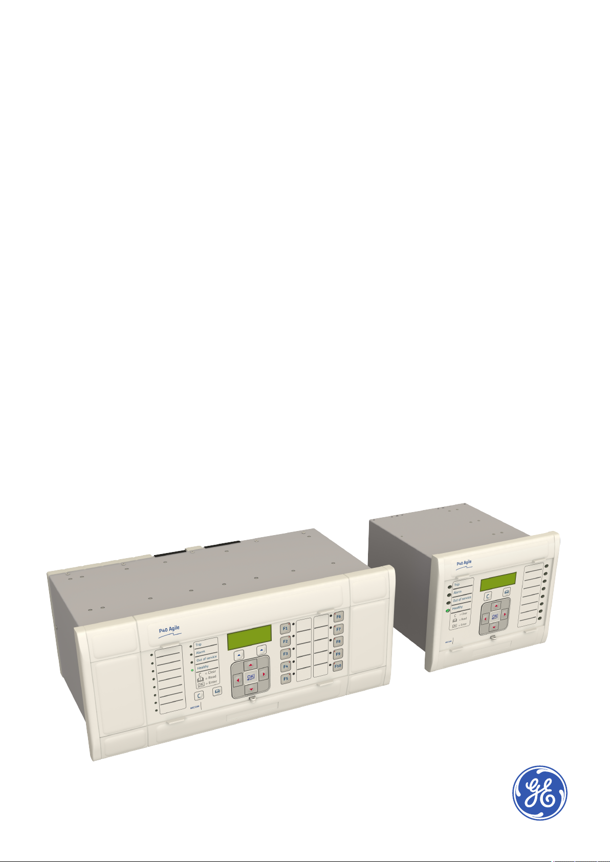
4 Front Panel 37
4.1 Front Panel 37
Page 4

Contents P543i/P545i
4.1.1 Front Panel Compartments 37
4.1.2 Keypad 38
4.1.3 Front Serial Port (SK1) 38
4.1.4 Front Parallel Port (SK2) 39
4.1.5 Fixed Function LEDs 39
4.1.6 Function Keys 39
4.1.7 Programable LEDs 40
5 Rear Panel 41
6 Boards and Modules 43
6.1 PCBs 43
6.2 Subassemblies 43
6.3 Main Processor Board 44
6.4 Power Supply Board 45
6.4.1 Watchdog 47
6.4.2 Rear Serial Port 48
6.5 Input Module - 1 Transformer Board 49
6.5.1 Input Module Circuit Description 50
6.5.2 Transformer Board 51
6.5.3 Input Board 52
6.6 Standard Output Relay Board 53
6.7 IRIG-B Board 54
6.8 Fibre Optic Board 55
6.9 Rear Communication Board 56
6.10 Ethernet Board 56
6.11 Redundant Ethernet Board 58
6.12 Coprocessor Board 60
6.12.1 Current Differential Inputs 60
6.12.2 Coprocessor board with 1PPS input 60
Chapter 4 Software Design 63
1 Chapter Overview 65
2 Sofware Design Overview 66
3 System Level Software 67
3.1 Real Time Operating System 67
3.2 System Services Software 67
3.3 Self-Diagnostic Software 67
3.4 Startup Self-Testing 67
3.4.1 System Boot 67
3.4.2 System Level Software Initialisation 68
3.4.3 Platform Software Initialisation and Monitoring 68
3.5 Continuous Self-Testing 68
4 Platform Software 70
4.1 Record Logging 70
4.2 Settings Database 70
4.3 Interfaces 70
5 Protection and Control Functions 71
5.1 Acquisition of Samples 71
5.2 Frequency Tracking 71
5.3 Direct Use of Sample Values 71
5.4 System Level Software Initialisation 71
5.5 Distance Protection 72
5.6 Fourier Signal Processing 72
5.7 Programmable Scheme Logic 73
5.8 Event Recording 74
5.9 Disturbance Recorder 74
5.10 Fault Locator 74
ii P54x1i-TM-EN-1
Page 5

P543i/P545i Contents
5.11 Function Key Interface 74
Chapter 5 Configuration 75
1 Chapter Overview 77
2 Settings Application Software 78
3 Using the HMI Panel 79
3.1 Navigating the HMI Panel 80
3.2 Getting Started 80
3.3 Default Display 81
3.4 Default Display Navigation 82
3.5 Password Entry 83
3.6 Processing Alarms and Records 83
3.7 Menu Structure 84
3.8 Changing the Settings 85
3.9 Direct Access (The Hotkey menu) 86
3.9.1 Setting Group Selection Using Hotkeys 86
3.9.2 Control Inputs 86
3.9.3 Circuit Breaker Control 87
3.10 Function Keys 87
4 Line Parameters 89
4.1 Tripping Mode 89
4.1.1 CB Trip Conversion Logic Diagram 89
4.2 Residual Compensation 90
4.3 Mutual Compensation 90
5 Date and Time Configuration 92
5.1 Using an SNTP Signal 92
5.2 Using an IRIG-B Signal 92
5.3 Using an IEEE 1588 PTP Signal 92
5.4 Without a Timing Source Signal 93
5.5 Time Zone Compensation 93
5.6 Daylight Saving Time Compensation 94
6 Settings Group Selection 95
Chapter 6 Current Differential Protection 97
1 Chapter Overview 99
2 Current Differential Protection Principle 100
2.1 Numerical Current Differential Protection 100
3 Synchronisation of Current Signals 102
3.1 Time Alignment using Ping-Pong Technique 102
3.2 GPS Synchronisation 103
4 Phase Current Differential Protection 105
4.1 Phase Current Differential Tripping Criteria 106
4.2 Phase Current Differential Protection Logic 107
5 Neutral Current Differential Protection 108
6 Three-Terminal Schemes 109
6.1 Three-Terminal Scheme Reconfiguration on Energisation 110
7 Transient Bias 111
8 Capacitive Charging Current Compensation 112
9 CT Compensation 113
10 Feeders with In-Zone Transformers 114
10.1 CT Phase Correction 114
10.2 Zero Sequence Filtering 115
10.3 Magnetising Inrush Restraint 116
10.3.1 Second Harmonic Restraint 117
10.4 Overfluxing Restraint 119
P54x1i-TM-EN-1 iii
Page 6

Contents P543i/P545i
10.4.1 Fifth Harmonic Blocking 119
10.5 Logic for Feeders with In-Zone Transformers 120
10.6 Second Harmonic Blocking Logic 121
10.7 Fifth Harmonic Blocking Logic 122
11 Current Differential Intertripping 123
12 Stub Bus Differential Protection 124
13 Application Notes 125
13.1 Setting Up the Phase Differential Characteristic 125
13.2 Sensitivity Under Heavy Loads 126
13.3 Permissive Intertripping 127
13.4 CT Ratio Correction Setting Guidelines 127
13.5 Feeders with Small Tapped Loads 128
13.6 Setting a Two-Terminal Phase Current Differential Element 128
13.7 Setting a Three-Terminal Phase Current Differential Element 129
Chapter 7 Distance Protection 133
1 Chapter Overview 135
2 Introduction 136
2.1 Distance Protection Principle 136
2.2 Performance Influencing Factors 136
2.3 Impedance Calculation 137
2.4 Implementation with Comparators 137
2.5 Polarization of Distance Characteristics 137
3 Distance Measuring Zones Operating Principles 138
3.1 Mho Characteristics 139
3.1.1 Directional Mho Characteristic for Phase Faults 139
3.1.2 Offset Mho Characteristic for Phase Faults 139
3.1.3 Directional Self-Polarized Mho Characteristic for Earth Faults 140
3.1.4 Offset Mho Characteristic for Earth Faults 142
3.1.5 Memory Polarization of Mho Characteristics 144
3.1.6 Dynamic Mho Expansion and Contraction 144
3.1.7 Cross Polarization of Mho Characteristics 147
3.1.8 Implementation of Mho Polarization 148
3.2 Quadrilateral Characteristic 149
3.2.1 Directional Quadrilaterals 150
3.2.2 Earth Fault Quadrilateral Characteristics 154
3.3 Quadrilateral Characteristic for Phase Faults 162
3.3.1 Phase Fault Impedance Reach Line 163
3.3.2 Phase Fault Reverse Impedance Reach Line 163
3.3.3 Phase Fault Resistive Reach Line 164
3.3.4 Phase Fault Reverse Resistive Reach Line 166
3.3.5 Phase Fault Quadrilateral Characteristic Summary 166
4 Phase and Earth Fault Distance Protection Implementation 168
4.1 Phase Fault Characteristics 168
4.2 Earth Fault Characteristics 168
4.3 Distance Protection Tripping Decision 168
4.4 Distance Protection Phase Selection 169
4.4.1 Faulted Phase Selection 169
4.5 Biased Neutral Current Detector 170
4.6 Distance Element Zone Settings 171
4.6.1 Directionalizing the Distance Elements 171
4.6.2 Advanced Distance Zone Settings 172
4.6.3 Distance Zone Sensitivities 172
4.7 Capacitor VT Applications 173
4.7.1 CVTs with Passive Suppression of Ferroresonance 173
4.7.2 CVTs with Active Suppression of Ferroresonance 173
4.8 Load Blinding 174
iv P54x1i-TM-EN-1
Page 7

P543i/P545i Contents
4.9 Cross Country Fault Protection 175
5 Delta Directional Element 176
5.1 Delta Directional Principle and Setup 176
5.2 Delta Directional Decision 177
6 Distance Isolated and Compensated Systems 179
6.1 Peterson Coil Earthed Systems 179
6.2 Earth Fault Distance Protection for Isolated and Compensated Systems 182
6.2.1 Single-phase to Earth Faults on Isolated or Compensated Systems 183
6.2.2 Cross-Country Faults on Isolated or Compensated Systems 183
6.3 Implementation of Distance Protection for Isolated and Compensated Networks 184
6.3.1 Network Earthing System Setting 184
6.3.2 First Earth FaultDetection 184
6.3.3 Fault Detection Logic 186
6.3.4 Phase Preferential Logic 187
7 Application Notes 193
7.1 Setting Mode Choice 193
7.2 Operating Characteristic Selection 193
7.2.1 Phase Characteristic 193
7.2.2 Earth Fault Characteristic 194
7.3 Zone Reach Setting Guidelines 194
7.3.1 Quadrilateral Resistive Reaches 195
7.4 Earth Fault Resistive Reaches and Tilting 195
7.4.1 Dynamic Tilting 196
7.4.2 Fixed Tilting 197
7.5 Phase Fault Zone Settings 197
7.6 Directional Element for Distance Protection 198
7.7 Filtering Setup 198
7.7.1 Distance Digital Filter 198
7.7.2 Setting up CVTs 198
7.8 Load Blinding Setup 199
7.9 Polarizing Setup 199
7.10 Delta Directional Element Setting Guidelines 200
7.10.1 Delta Thresholds 200
7.11 Distance Protection Worked Example 201
7.11.1 Line Impedance Calculation 202
7.11.2 Residual Compensation for Earth Fault Elements 202
7.11.3 Zone 1 Phase and Ground Reach Settings 202
7.11.4 Zone 2 Phase and Ground Reach Settings 203
7.11.5 Zone 3 Phase and Ground Reach Settings 203
7.11.6 Zone 3 Reverse Reach Settings 203
7.11.7 Zone 4 Reverse Reach Settings 203
7.11.8 Load Avoidance 204
7.11.9 Quadrilateral Resistive Reach Settings 204
7.12 Teed Feeder Applications 206
Chapter 8 Carrier Aided Schemes 207
1 Chapter Overview 209
2 Introduction 210
3 Carrier Aided Schemes Implementation 211
3.1 Carrier Aided Scheme Types 211
3.2 Default Carrier Aided Schemes 212
4 Aided Distance Scheme Logic 213
4.1 Permissive Underreach Scheme 213
4.2 Permissive Over-reach Scheme 214
4.2.1 Permissive Overreach Trip Reinforcement 216
4.2.2 Permissive Overreach Weak Infeed Features 217
4.3 Permissive Scheme Loss Of Guard 217
P54x1i-TM-EN-1 v
Page 8

Contents P543i/P545i
4.4 Current Reversal Guard Logic 218
4.5 Aided Distance Blocking Schemes 219
4.6 Aided Distance Unblocking Schemes 220
4.7 Aided Distance Logic Diagrams 222
4.7.1 Aided Distance Send Logic 222
4.7.2 Carrier Aided Schemes Receive Logic 223
4.7.3 Aided Distance Tripping Logic 223
4.7.4 PUR Aided Tripping logic 224
4.7.5 POR Aided Tripping logic 225
4.7.6 Aided Scheme Blocking 1 Tripping logic 226
4.7.7 Aided Scheme Blocking 2 Tripping logic 226
5 Aided DEF Scheme Logic 227
5.1 Aided DEF Introduction 227
5.2 Implementation 227
5.3 Aided DEF Polarization 227
5.3.1 Zero Sequence Polarizing 228
5.3.2 Negative Sequence Polarizing 229
5.4 Aided DEF Setting Guidelines 230
5.5 Aided DEF POR Scheme 231
5.6 Aided DEF Blocking Scheme 232
5.7 Aided DEF Logic Diagrams 233
5.7.1 DEF Directional Signals 233
5.7.2 Aided DEF Send Logic 234
5.7.3 Carrier Aided Schemes Receive Logic 234
5.7.4 Aided DEF Tripping Logic 235
5.7.5 POR Aided Tripping logic 236
5.7.6 Aided Scheme Blocking 1 Tripping logic 237
5.7.7 Aided Scheme Blocking 2 Tripping logic 237
6 Aided Delta Scheme Logic 238
6.1 Aided Delta POR Scheme 238
6.2 Aided Delta Blocking Scheme 239
6.3 Aided Delta Logic Diagrams 241
6.3.1 Aided Delta Send Logic 241
6.3.2 Carrier Aided Schemes Receive Logic 241
6.3.3 Aided Delta Tripping Logic 242
6.3.4 POR Aided Tripping logic 243
6.3.5 Aided Scheme Blocking 1 Tripping logic 244
6.3.6 Aided Scheme Blocking 2 Tripping logic 244
7 Application Notes 245
7.1 Aided Distance PUR Scheme 245
7.2 Aided Distance POR Scheme 245
7.3 Aided Distance Blocking Scheme 245
7.4 Aided DEF POR Scheme 246
7.5 Aided DEF Blocking Scheme 246
7.6 Aided Delta POR Scheme 246
7.7 Aided Delta Blocking Scheme 246
7.8 Teed Feeder Applications 247
7.8.1 POR Schemes for Teed Feeders 248
7.8.2 PUR Schemes for Teed Feeders 248
7.8.3 Blocking Schemes for Teed Feeders 249
Chapter 9 Non-Aided Schemes 251
1 Chapter Overview 253
2 Non-Aided Schemes 254
3 Basic Schemes 255
3.1 Basic Scheme Modes 255
3.2 Basic Scheme Setting 258
vi P54x1i-TM-EN-1
Page 9

P543i/P545i Contents
4 Trip On Close Schemes 259
4.1 Switch On To Fault (SOTF) 260
4.1.1 Switch Onto Fault Mode 260
4.1.2 SOTF Tripping 261
4.1.3 SOTF Tripping with CNV 261
4.2 Trip On Reclose (TOR) 261
4.2.1 Trip On Reclose Mode 262
4.2.2 TOR Tripping Logic for Appropriate Zones 262
4.2.3 TOR Tripping Logic with CNV 262
4.3 Polarisation during Circuit Engergisation 262
5 Zone1 Extension Scheme 264
6 Loss of Load Scheme 265
Chapter 10 Power Swing Functions 267
1 Chapter Overview 269
2 Introduction to Power Swing Blocking 270
3 Power Swing Blocking 272
3.1 Power Swing Detection 272
3.1.1 Settings-Free Power Swing Detection 272
3.1.2 Slow Power Swing Detection 275
3.2 Detection of a Fault During a Power Swing 276
3.3 Power Swing Blocking Configuration 276
3.4 Power Swing Load Blinding Boundary 277
3.5 Power Swing Blocking Logic 278
3.6 Power Swing Blocking Setting Guidelines 279
3.6.1 Setting the Resistive Limits 280
3.6.2 Setting the Reactive Limits 280
3.6.3 PSB Timer Setting Guidelines 281
4 Out of Step Protection 283
4.1 Out of Step Detection 283
4.2 Out of Step Protection Operataing Principle 284
4.3 Out of Step Logic Diagram 285
4.4 OST Application Notes 285
4.4.1 Setting the OST Mode 285
Chapter 11 Autoreclose 293
1 Chapter Overview 295
2 Introduction to Autoreclose 296
3 Autoreclose Implementation 297
3.1 Autoreclose Logic Inputs from External Sources 298
3.1.1 Circuit Breaker Healthy Input 298
3.1.2 Inhibit Autoreclose Input 298
3.1.3 Block Autoreclose Input 298
3.1.4 Reset Lockout Input 299
3.1.5 Pole Discrepancy Input 299
3.1.6 External Trip Indication 299
3.2 Autoreclose Logic Inputs 299
3.2.1 Trip Initiation Signals 299
3.2.2 Circuit Breaker Status Inputs 299
3.2.3 System Check Signals 299
3.3 Autoreclose Logic Outputs 299
3.4 Autoreclose Operating Sequence 300
3.4.1 AR Timing Sequence - Transient Fault 300
3.4.2 AR Timing Sequence - Evolving/Permanent Fault 300
3.4.3 AR Timing Sequence - Evolving/Permanent Fault Single-phase 301
4 Autoreclose System Map 302
P54x1i-TM-EN-1 vii
Page 10

Contents P543i/P545i
4.1 Autoreclose System Map Diagrams 304
4.2 Autoreclose Internal Signals 309
4.3 Autoreclose DDB Signals 311
5 Logic Modules 317
5.1 Circuit Breaker Status Monitor 317
5.1.1 CB State Monitor Logic diagram 318
5.2 Circuit Breaker Open Logic 319
5.2.1 Circuit Breaker Open Logic Diagram 319
5.3 Circuit Breaker in Service Logic 319
5.3.1 Circuit Breaker in Service Logic Diagram 319
5.3.2 Autoreclose OK Logic Diagram 320
5.4 Autoreclose Enable 320
5.4.1 Autoreclose Enable Logic Diagram 320
5.5 Autoreclose Modes 320
5.5.1 Single-Phase and Three-Phase Autoreclose 321
5.5.2 Autoreclose Modes Enable Logic Diagram 322
5.6 AR Force Three-Phase Trip Logic 322
5.6.1 AR Force Three-Phase Trip Logic Diagram 322
5.7 Autoreclose Initiation Logic 322
5.7.1 Autoreclose Initiation Logic Diagram 324
5.7.2 Autoreclose Trip Test Logic Diagram 324
5.7.3 AR External Trip Initiation Logic Diagram 325
5.7.4 Protection Reoperation and Evolving Fault Logic Diagram 326
5.7.5 Fault Memory Logic Diagram 326
5.8 Autoreclose In Progress 326
5.8.1 Autoreclose In Progress Logic Diagram 327
5.9 Sequence Counter 327
5.9.1 Autoreclose Sequence Counter Logic Diagram 328
5.10 Autoreclose Cycle Selection 328
5.10.1 Single-Phase Autoreclose Cycle Selection Logic Diagram 328
5.10.2 3-phase Autoreclose Cycle Selection 329
5.11 Dead Time Control 329
5.11.1 Dead Time Start Enable Logic Diagram 330
5.11.2 1-phase Dead Time Logic Diagram 331
5.11.3 3-phase Dead Time Logic Diagram 332
5.12 Circuit Breaker Autoclose 332
5.12.1 Circuit Breaker Autoclose Logic Diagram 333
5.13 Reclaim Time 333
5.13.1 Prepare Reclaim Initiation Logic Diagram 334
5.13.2 Reclaim Time Logic Diagram 334
5.13.3 Succesful Autoreclose Signals Logic Diagram 335
5.13.4 Autoreclose Reset Successful Indication Logic Diagram 335
5.14 CB Healthy and System Check Timers 335
5.14.1 CB Healthy and System Check Timers Logic Diagram 336
5.15 Autoreclose Shot Counters 336
5.15.1 Autoreclose Shot Counters Logic Diagram 337
5.16 Circuit Breaker Control 338
5.16.1 CB Control Logic Diagram 338
5.17 Circuit Breaker Trip Time Monitoring 339
5.17.1 CB Trip Time Monitoring Logic Diagram 339
5.18 Autoreclose Lockout 339
5.18.1 CB Lockout Logic Diagram 340
5.19 Reset Circuit Breaker Lockout 341
5.19.1 Reset CB Lockout Logic Diagram 341
5.20 Pole Discrepancy 342
5.20.1 Pole Discrepancy Logic Diagram 342
5.21 Circuit Breaker Trip Conversion 342
5.21.1 CB Trip Conversion Logic Diagram 343
viii P54x1i-TM-EN-1
Page 11

P543i/P545i Contents
5.22 Monitor Checks for CB Closure 343
5.22.1 Check Synchronisation Monitor for CB Closure 344
5.22.2 Voltage Monitor for CB Closure 345
5.23 Synchronisation Checks for CB Closure 345
5.23.1 Three-phase Autoreclose System Check Logic Diagram 347
5.23.2 CB Manual Close System Check Logic Diagram 348
6 Setting Guidelines 349
6.1 De-ionising Time Guidance 349
6.2 Dead Timer Setting Guidelines 349
6.2.1 Example Dead Time Calculation 349
6.3 Reclaim Time Setting Guidelines 350
Chapter 12 CB Fail Protection 351
1 Chapter Overview 353
2 Circuit Breaker Fail Protection 354
3 Circuit Breaker Fail Implementation 355
3.1 Circuit Breaker Fail Timers 355
3.2 Zero Crossing Detection 355
4 Circuit Breaker Fail Logic 357
4.1 Circuit Breaker Fail Logic - Part 1 357
4.2 Circuit Breaker Fail Logic - Part 2 358
4.3 Circuit Breaker Fail Logic - Part 3 359
4.4 Circuit Breaker Fail Logic - Part 4 360
5 Application Notes 361
5.1 Reset Mechanisms for CB Fail Timers 361
5.2 Setting Guidelines (CB fail Timer) 361
5.3 Setting Guidelines (Undercurrent) 362
Chapter 13 Current Protection Functions 363
1 Chapter Overview 365
2 Phase Fault Overcurrent Protection 366
2.1 POC Implementation 366
2.2 Directional Element 366
2.3 POC Logic 368
3 Negative Sequence Overcurrent Protection 369
3.1 Negative Sequence Overcurrent Protection Implementation 369
3.2 Directional Element 369
3.3 NPSOC Logic 370
3.4 Application Notes 370
3.4.1 Setting Guidelines (Current Threshold) 370
3.4.2 Setting Guidelines (Time Delay) 370
3.4.3 Setting Guidelines (Directional element) 371
4 Earth Fault Protection 372
4.1 Earth Fault Protection Implementation 372
4.2 IDG Curve 372
4.3 Directional Element 373
4.3.1 Residual Voltage Polarisation 373
4.3.2 Negative Sequence Polarisation 374
4.4 Earth Fault Protection Logic 375
4.5 Application Notes 375
4.5.1 Residual Voltage Polarisation Setting Guidelines 375
4.5.2 Setting Guidelines (Directional Element) 375
5 Sensitive Earth Fault Protection 377
5.1 SEF Protection Implementation 377
5.2 EPATR B Curve 377
P54x1i-TM-EN-1 ix
Page 12

Contents P543i/P545i
5.3 Sensitive Earth Fault Protection Logic 378
5.4 Application Notes 379
5.4.1 Insulated Systems 379
5.4.2 Setting Guidelines (Insulated Systems) 380
6 High Impedance REF 382
6.1 High Impedance REF Principle 382
7 Thermal Overload Protection 384
7.1 Single Time Constant Characteristic 384
7.2 Dual Time Constant Characteristic 384
7.3 Thermal Overload Protection Implementation 385
7.4 Thermal Overload Protection Logic 385
7.5 Application Notes 385
7.5.1 Setting Guidelines for Dual Time Constant Characteristic 385
7.5.2 Setting Guidelines for Single Time Constant Characteristic 387
8 Broken Conductor Protection 389
8.1 Broken Conductor Protection Implementation 389
8.2 Broken Conductor Protection Logic 389
8.3 Application Notes 389
8.3.1 Setting Guidelines 389
9 Transient Earth Fault Detection 391
9.1 Transient Earth Fault Detection Implementation 392
9.2 Transient Earth Fault Detection Logic 393
9.2.1 Transient Earth Fault Detection Logic Overview 393
9.2.2 Fault Type Detector Logic 394
9.2.3 Direction Detector Logic - Standard Mode 394
9.2.4 Transient Earth Fault Detection Output Alarm Logic 394
Chapter 14 Voltage Protection Functions 395
1 Chapter Overview 397
2 Undervoltage Protection 398
2.1 Undervoltage Protection Implementation 398
2.2 Undervoltage Protection Logic 399
2.3 Application Notes 400
2.3.1 Undervoltage Setting Guidelines 400
3 Overvoltage Protection 401
3.1 Overvoltage Protection Implementation 401
3.2 Overvoltage Protection Logic 402
3.3 Application Notes 403
3.3.1 Overvoltage Setting Guidelines 403
4 Compensated Overvoltage 404
5 Residual Overvoltage Protection 405
5.1 Residual Overvoltage Protection Implementation 405
5.2 Residual Overvoltage Logic 406
5.3 Application Notes 406
5.3.1 Calculation for Solidly Earthed Systems 406
5.3.2 Calculation for Impedance Earthed Systems 407
5.3.3 Setting Guidelines 408
Chapter 15 Frequency Protection Functions 409
1 Chapter Overview 411
2 Frequency Protection 412
2.1 Underfrequency Protection 412
2.1.1 Underfrequency Protection Implementation 412
2.1.2 Underfrequency Protection logic 413
2.1.3 Application Notes 413
x P54x1i-TM-EN-1
Page 13

P543i/P545i Contents
2.2 Overfrequency Protection 413
2.2.1 Overfrequency Protection Implementation 413
2.2.2 Overfrequency Protection logic 414
2.2.3 Application Notes 414
3 Independent R.O.C.O.F Protection 415
3.1 Indepenent R.O.C.O.F Protection Implementation 415
3.2 Independent R.O.C.O.F Protection Logic 415
Chapter 16 Current Transformer Requirements 417
1 Chapter Overview 419
2 Recommended CT Classes 420
3 Current Differential Requirements 421
4 Distance Protection Requirements 422
5 Determining Vk for IEEE C-class CT 423
6 Worked Examples 424
6.1 Calculation of Primary X/R ratio 424
6.2 Calculation of Source Impedance 424
6.3 Calculation of Full Line Impedance 424
6.4 Calculation of Total Impedance up to Remote Busbar 425
6.5 Calculation of Through Fault X/R ratio 425
6.6 Calculation of Through Fault Current 425
6.7 Calculation of Line Impedance to Zone 1 Reach Point 425
6.8 Calculation of Total Impedance to Zone 1 Reach Point 425
6.9 Calculation of X/R to Zone 1 Reach Point 425
6.10 Calculation of Fault Current to Zone 1 Reach Point 425
6.11 Calculation of Vk for Current Differential Protection 425
6.12 Calculation of Vk for Distance Zone 1 Reach Point 425
6.13 Calculation of Vk for Distance Zone 1 Close-up Fault 426
6.14 Calculation of Vk for Distance Time Delayed Zones 426
6.15 Overcurrent Elements 426
6.16 Overcurrent Elements 426
Chapter 17 Monitoring and Control 427
1 Chapter Overview 429
2 Event Records 430
2.1 Event Types 430
2.1.1 Opto-input Events 431
2.1.2 Contact Events 431
2.1.3 Alarm Events 431
2.1.4 Fault Record Events 432
2.1.5 Maintenance Events 432
2.1.6 Protection Events 432
2.1.7 Security Events 433
2.1.8 Platform Events 433
3 Disturbance Recorder 434
4 Measurements 435
4.1 Measured Quantities 435
4.2 Measurement Setup 435
4.3 Fault Locator 435
4.4 Opto-input Time Stamping 435
5 CB Condition Monitoring 436
5.1 Broken Current Accumulator 437
5.2 CB Trip Counter 437
5.3 CB Operating Time Accumulator 438
5.4 Excessive Fault Frequency Counter 438
P54x1i-TM-EN-1 xi
Page 14

Contents P543i/P545i
5.5 Reset Lockout Alarm 439
5.6 CB Condition Monitoring Logic 440
5.7 Reset Circuit Breaker Lockout 440
5.7.1 Reset CB Lockout Logic Diagram 441
5.8 Application Notes 441
5.8.1 Setting the Thresholds for the Total Broken Current 441
5.8.2 Setting the thresholds for the Number of Operations 442
5.8.3 Setting the thresholds for the Operating Time 442
5.8.4 Setting the Thresholds for Excesssive Fault Frequency 442
6 CB State Monitoring 443
6.1 CB State Monitor Logic diagram 444
7 Circuit Breaker Control 445
7.1 CB Control using the IED Menu 445
7.2 CB Control using the Hotkeys 446
7.3 CB Control using the Function Keys 446
7.4 CB Control using the Opto-inputs 447
7.5 Remote CB Control 447
7.6 CB Healthy Check 448
7.7 Synchronisation Check 448
7.8 CB Control AR Implications 448
7.9 CB Control Logic Diagram 449
8 Pole Dead Function 450
8.1 Pole Dead Logic 450
9 System Checks 451
9.1 System Checks Implementation 451
9.1.1 VT Connections 451
9.1.2 Voltage Monitoring 452
9.1.3 Check Synchronisation 452
9.1.4 Check Syncronisation Vector Diagram 452
9.2 Voltage Monitor for CB Closure 454
9.3 Check Synchronisation Monitor for CB Closure 455
9.4 System Check PSL 456
9.5 Application Notes 456
9.5.1 Predictive Closure of Circuit Breaker 456
9.5.2 Voltage and Phase Angle Correction 456
Chapter 18 Supervision 459
1 Chapter Overview 461
2 Current Differential Supervision 462
2.1 Current Differential Starter Supervision 462
2.1.1 Current Differential Starter Supervision Logic 464
2.1.2 Current Differential Start Logic 465
2.2 Switched Communication Path Supervision 465
2.3 Communications Asymmetry Supervision 466
2.4 GPS Synchronisation Supervision 467
2.4.1 Propogation Delay Management 468
3 Voltage Transformer Supervision 470
3.1 Loss of One or Two Phase Voltages 470
3.2 Loss of all Three Phase Voltages 470
3.3 Absence of all Three Phase Voltages on Line Energisation 470
3.4 VTS Implementation 471
3.5 VTS Logic 472
4 Current Transformer Supervision 475
4.1 Differential CTS 475
4.2 Differential CTS Logic 476
4.3 CTS Implementation 476
xii P54x1i-TM-EN-1
Page 15

P543i/P545i Contents
4.4 Standard CTS Logic 477
4.5 CTS Blocking 477
4.6 Application Notes 477
4.6.1 Setting Guidelines 477
4.6.2 Differential CTS Setting Guidelines 478
5 Trip Circuit Supervision 479
5.1 Trip Circuit Supervision Scheme 1 479
5.1.1 Resistor Values 479
5.1.2 PSL for TCS Scheme 1 480
5.2 Trip Circuit Supervision Scheme 2 480
5.2.1 Resistor Values 481
5.2.2 PSL for TCS Scheme 2 481
5.3 Trip Circuit Supervision Scheme 3 481
5.3.1 Resistor Values 482
5.3.2 PSL for TCS Scheme 3 482
Chapter 19 Digital I/O and PSL Configuration 483
1 Chapter Overview 485
2 Configuring Digital Inputs and Outputs 486
3 Scheme Logic 487
3.1 PSL Editor 488
3.2 PSL Schemes 488
3.3 PSL Scheme Version Control 488
4 Configuring the Opto-Inputs 489
5 Assigning the Output Relays 490
6 Fixed Function LEDs 491
6.1 Trip LED Logic 491
7 Configuring Programmable LEDs 492
8 Function Keys 494
9 Control Inputs 495
Chapter 20 Fibre Teleprotection 497
1 Chapter Overview 499
2 Protection Signalling Introduction 500
2.1 Unit Protection Schemes 500
2.2 Teleprotection Commands 500
2.3 Transmission Media and Interference 501
3 Fibre Teleprotection Implementation 502
3.1 Setting up the IM64 Scheme 502
3.1.1 Fibre Teleprotection Scheme Terminal Addressing 503
3.1.2 Setting up IM64 504
3.1.3 Two-Terminal IM64 Operation 504
3.1.4 Dual Redundant Two-Terminal IM64 Operation 504
3.1.5 Three-Terminal IM64 Operation 505
3.1.6 Physical Connection 506
3.2 Communications Supervision 509
4 IM64 Logic 511
5 Application Notes 513
5.1 Alarm Management 513
5.2 Alarm Logic 513
5.3 Two-ended Scheme Extended Supervision 514
5.4 Three-ended Scheme Extended Supervision 514
Chapter 21 Electrical Teleprotection 517
P54x1i-TM-EN-1 xiii
Page 16

Contents P543i/P545i
1 Chapter Overview 519
2 Introduction 520
3 Teleprotection Scheme Principles 521
3.1 Direct Tripping 521
3.2 Permissive Tripping 521
4 Implementation 522
5 Configuration 523
6 Connecting to Electrical InterMiCOM 525
6.1 Short Distance 525
6.2 Long Distance 525
7 Application Notes 526
Chapter 22 Communications 529
1 Chapter Overview 531
2 Communication Interfaces 532
3 Serial Communication 533
3.1 EIA(RS)232 Bus 533
3.2 EIA(RS)485 Bus 533
3.2.1 EIA(RS)485 Biasing Requirements 534
3.3 K-Bus 534
4 Standard Ethernet Communication 536
4.1 Hot-Standby Ethernet Failover 536
5 Redundant Ethernet Communication 537
5.1 Supported Protocols 537
5.2 Parallel Redundancy Protocol 538
5.3 High-Availability Seamless Redundancy (HSR) 539
5.3.1 HSR Multicast Topology 539
5.3.2 HSR Unicast Topology 540
5.3.3 HSR Application in the Substation 540
5.4 Rapid Spanning Tree Protocol 541
5.5 Self Healing Protocol 542
5.6 Dual Homing Protocol 543
5.7 Configuring IP Addresses 545
5.7.1 Configuring the IED IP Address 546
5.7.2 Configuring the REB IP Address 546
5.8 PRP/HSR Configurator 549
5.8.1 Connecting the IED to a PC 549
5.8.2 Installing the Configurator 550
5.8.3 Starting the Configurator 550
5.8.4 PRP/HSR Device Identification 551
5.8.5 Selecting the Device Mode 551
5.8.6 PRP/HSR IP Address Configuration 551
5.8.7 SNTP IP Address Configuration 551
5.8.8 Check for Connected Equipment 551
5.8.9 PRP Configuration 551
5.8.10 HSR Configuration 552
5.8.11 Filtering Database 552
5.8.12 End of Session 553
5.9 RSTP Configurator 553
5.9.1 Connecting the IED to a PC 553
5.9.2 Installing the Configurator 554
5.9.3 Starting the Configurator 554
5.9.4 RSTP Device Identification 554
5.9.5 RSTP IP Address Configuration 555
5.9.6 SNTP IP Address Configuration 555
5.9.7 Check for Connected Equipment 555
5.9.8 RSTP Configuration 555
xiv P54x1i-TM-EN-1
Page 17

P543i/P545i Contents
5.9.9 End of Session 556
5.10 Switch Manager 556
5.10.1 Installation 557
5.10.2 Setup 558
5.10.3 Network Setup 558
5.10.4 Bandwidth Used 558
5.10.5 Reset Counters 558
5.10.6 Check for Connected Equipment 558
5.10.7 Mirroring Function 559
5.10.8 Ports On/Off 559
5.10.9 VLAN 559
5.10.10 End of Session 559
6 Simple Network Management Protocol (SNMP) 560
6.1 SNMP Management Information Bases 560
6.2 Main Processor MIBS Structure 560
6.3 Redundant Ethernet Board MIB Structure 561
6.4 Accessing the MIB 565
6.5 Main Processor SNMP Configuration 565
7 Data Protocols 567
7.1 Courier 567
7.1.1 Physical Connection and Link Layer 567
7.1.2 Courier Database 568
7.1.3 Settings Categories 568
7.1.4 Setting Changes 568
7.1.5 Event Extraction 568
7.1.6 Disturbance Record Extraction 570
7.1.7 Programmable Scheme Logic Settings 570
7.1.8 Time Synchronisation 570
7.1.9 Courier Configuration 571
7.2 IEC 60870-5-103 572
7.2.1 Physical Connection and Link Layer 572
7.2.2 Initialisation 573
7.2.3 Time Synchronisation 573
7.2.4 Spontaneous Events 573
7.2.5 General Interrogation (GI) 573
7.2.6 Cyclic Measurements 573
7.2.7 Commands 573
7.2.8 Test Mode 574
7.2.9 Disturbance Records 574
7.2.10 Command/Monitor Blocking 574
7.2.11 IEC 60870-5-103 Configuration 574
7.3 DNP 3.0 575
7.3.1 Physical Connection and Link Layer 576
7.3.2 Object 1 Binary Inputs 576
7.3.3 Object 10 Binary Outputs 576
7.3.4 Object 20 Binary Counters 577
7.3.5 Object 30 Analogue Input 577
7.3.6 Object 40 Analogue Output 578
7.3.7 Object 50 Time Synchronisation 578
7.3.8 DNP3 Device Profile 578
7.3.9 DNP3 Configuration 586
7.4 IEC 61850 587
7.4.1 Benefits of IEC 61850 588
7.4.2 IEC 61850 Interoperability 588
7.4.3 The IEC 61850 Data Model 588
7.4.4 IEC 61850 in MiCOM IEDs 589
7.4.5 IEC 61850 Data Model Implementation 590
7.4.6 IEC 61850 Communication Services Implementation 590
7.4.7 IEC 61850 Peer-to-peer (GOOSE) communications 590
P54x1i-TM-EN-1 xv
Page 18

Contents P543i/P545i
7.4.8 Mapping GOOSE Messages to Virtual Inputs 590
7.4.9 Ethernet Functionality 591
7.4.10 IEC 61850 Configuration 591
7.4.11 IEC 61850 Edition 2 592
8 Read Only Mode 596
8.1 IEC 60870-5-103 Protocol Blocking 596
8.2 Courier Protocol Blocking 596
8.3 IEC 61850 Protocol Blocking 597
8.4 Read-Only Settings 597
8.5 Read-Only DDB Signals 597
9 Time Synchronisation 598
9.1 Demodulated IRIG-B 598
9.1.1 IRIG-B Implementation 599
9.2 SNTP 599
9.2.1 Loss of SNTP Server Signal Alarm 599
9.3 IEEE 1588 Precision time Protocol 599
9.3.1 Accuracy and Delay Calculation 599
9.3.2 PTP Domains 600
9.4 Time Synchronsiation using the Communication Protocols 600
Chapter 23 Cyber-Security 601
1 Overview 603
2 The Need for Cyber-Security 604
3 Standards 605
3.1 NERC Compliance 605
3.1.1 CIP 002 606
3.1.2 CIP 003 606
3.1.3 CIP 004 606
3.1.4 CIP 005 606
3.1.5 CIP 006 606
3.1.6 CIP 007 607
3.1.7 CIP 008 607
3.1.8 CIP 009 607
3.2 IEEE 1686-2007 607
4 Cyber-Security Implementation 609
4.1 NERC-Compliant Display 609
4.2 Four-level Access 610
4.2.1 Blank Passwords 611
4.2.2 Password Rules 611
4.2.3 Access Level DDBs 612
4.3 Enhanced Password Security 612
4.3.1 Password Strengthening 612
4.3.2 Password Validation 612
4.3.3 Password Blocking 613
4.4 Password Recovery 614
4.4.1 Password Recovery 614
4.4.2 Password Encryption 615
4.5 Disabling Physical Ports 615
4.6 Disabling Logical Ports 615
4.7 Security Events Management 616
4.8 Logging Out 618
Chapter 24 Installation 619
1 Chapter Overview 621
2 Handling the Goods 622
2.1 Receipt of the Goods 622
xvi P54x1i-TM-EN-1
Page 19

P543i/P545i Contents
2.2 Unpacking the Goods 622
2.3 Storing the Goods 622
2.4 Dismantling the Goods 622
3 Mounting the Device 623
3.1 Flush Panel Mounting 623
3.2 Rack Mounting 624
4 Cables and Connectors 626
4.1 Terminal Blocks 626
4.2 Power Supply Connections 627
4.3 Earth Connnection 627
4.4 Current Transformers 627
4.5 Voltage Transformer Connections 628
4.6 Watchdog Connections 628
4.7 EIA(RS)485 and K-Bus Connections 628
4.8 IRIG-B Connection 628
4.9 Opto-input Connections 628
4.10 Output Relay Connections 628
4.11 Ethernet Metallic Connections 629
4.12 Ethernet Fibre Connections 629
4.13 RS232 connection 629
4.14 Download/Monitor Port 629
4.15 GPS Fibre Connection 629
4.16 Fibre Communication Connections 629
5 Case Dimensions 630
5.1 Case Dimensions 40TE 630
5.2 Case Dimensions 60TE 631
5.3 Case Dimensions 80TE 632
Chapter 25 Commissioning Instructions 633
1 Chapter Overview 635
2 General Guidelines 636
3 Commissioning Test Menu 637
3.1 Opto I/P Status Cell (Opto-input Status) 637
3.2 Relay O/P Status Cell (Relay Output Status) 637
3.3 Test Port Status Cell 637
3.4 Monitor Bit 1 to 8 Cells 637
3.5 Test Mode Cell 638
3.6 Test Pattern Cell 638
3.7 Contact Test Cell 638
3.8 Test LEDs Cell 638
3.9 Test Autoreclose Cell 638
3.10 Static Test Mode 639
3.11 Loopback Mode 639
3.12 IM64 Test Pattern 640
3.13 IM64 Test Mode 640
3.14 Red and Green LED Status Cells 640
3.15 Using a Monitor Port Test Box 640
4 Commissioning Equipment 641
4.1 Recommended Commissioning Equipment 641
4.2 Essential Commissioning Equipment 641
4.3 Advisory Test Equipment 642
5 Product Checks 643
5.1 Product Checks with the IED De-energised 643
5.1.1 Visual Inspection 644
5.1.2 Current Transformer Shorting Contacts 644
5.1.3 Insulation 644
P54x1i-TM-EN-1 xvii
Page 20

Contents P543i/P545i
5.1.4 External Wiring 644
5.1.5 Watchdog Contacts 645
5.1.6 Power Supply 645
5.2 Product Checks with the IED Energised 645
5.2.1 Watchdog Contacts 645
5.2.2 Test LCD 646
5.2.3 Date and Time 646
5.2.4 Test LEDs 647
5.2.5 Test Alarm and Out-of-Service LEDs 647
5.2.6 Test Trip LED 647
5.2.7 Test User-programmable LEDs 647
5.2.8 Test Field Voltage Supply 647
5.2.9 Test Opto-inputs 647
5.2.10 Test Output Relays 648
5.2.11 Test Serial Communication Port RP1 648
5.2.12 Test Serial Communication Port RP2 649
5.2.13 Test Ethernet Communication 650
5.3 Secondary Injection Tests 650
5.3.1 Test Current Inputs 650
5.3.2 Test Voltage Inputs 651
6 Electrical Intermicom Communication Loopback 652
6.1 Setting up the Loopback 652
6.2 Loopback Test 652
6.2.1 InterMicom Command Bits 653
6.2.2 InterMicom Channel Diagnostics 653
6.2.3 Simulating a Channel Failure 653
7 Intermicom 64 Communication 654
7.1 Checking the Interface 654
7.2 Setting up the Loopback 655
7.3 Loopback Test 655
8 GPS Synchronisation 656
8.1 GPS Optical Signal Strength 656
8.2 Check Synchronisation signal at the IED 656
9 Setting Checks 657
9.1 Apply Application-specific Settings 657
9.1.1 Transferring Settings from a Settings File 657
9.1.2 Entering settings using the HMI 657
10 IEC 61850 Edition 2 Testing 659
10.1 Using IEC 61850 Edition 2 Test Modes 659
10.1.1 IED Test Mode Behaviour 659
10.1.2 Sampled Value Test Mode Behaviour 659
10.2 Simulated Input Behaviour 660
10.3 Testing Examples 660
10.3.1 Test Procedure for Real Values 661
10.3.2 Test Procedure for Simulated Values - No Plant 661
10.3.3 Test Procedure for Simulated Values - With Plant 662
10.3.4 Contact Test 663
11 Current Differential Protection 664
11.1 Current Differential Bias Characteristic 664
11.1.1 Lower Slope 664
11.1.2 Upper Slope 665
11.2 Current Differential Operation and Contact Assignment 665
12 Distance Protection 667
12.1 Dependency Conditions 667
12.2 Distance Protection Single-ended Testing 667
12.2.1 Preliminaries 667
12.2.2 Zone 1 Reach Check 668
12.2.3 Zone 2 Reach Check 668
xviii P54x1i-TM-EN-1
Page 21

P543i/P545i Contents
12.2.4 Zone 3 Reach Check 669
12.2.5 Zone 4 Reach Check 669
12.2.6 Zone P Reach Check 669
12.2.7 Zone Q Reach Check 669
12.2.8 Resistive Reach 669
12.2.9 Load Blinder 670
12.3 Operation and Contact Assignment 670
12.3.1 Phase A 670
12.3.2 Phase B 670
12.3.3 Phase C 670
12.3.4 Time Delay Settings 671
12.4 Scheme Testing 671
12.4.1 Scheme Trip Test for Zone 1 Extension 672
12.4.2 Scheme Trip Tests for Permissive Schemes 672
12.4.3 Scheme Trip Tests for Blocking Scheme 672
12.4.4 Signal Send Test for Permissive Schemes 673
12.4.5 Signal Send Test for Blocking Scheme 673
12.4.6 Scheme Timer Settings 673
13 Delta Directional Comparison 674
13.1 Single-ended Testing 674
13.1.1 Preliminaries 674
13.1.2 Single-ended Injection Test 674
13.1.3 Forward Fault Preparation 674
13.2 Operation and Contact Assignment 675
13.2.1 Phase A 675
13.2.2 Phase B 675
13.2.3 Phase C 675
13.3 Delta Protection Scheme Testing 676
13.3.1 Signal Send Test for Permissive Schemes 676
13.3.2 Signal Send Test for Blocking Schemes 676
14 DEF Aided Schemes 677
14.1 Dependency Conditions 677
14.2 Earth Current Pilot Scheme 677
14.2.1 Preliminaries 678
14.2.2 Perform the Test 678
14.2.3 Forward Fault Trip Test 678
14.3 Scheme Testing 679
14.3.1 Signal Send Test for Permissive Schemes 679
14.3.2 Signal Send Test for Blocking Schemes 679
15 Out of Step Protection 680
15.1 OST Setting 680
15.2 Predictive OST Setting 681
15.3 Predictive and OST Setting 681
15.4 OST Timer Test 681
16 Protection Timing Checks 682
16.1 Dependency Conditions 682
16.2 Overcurrent Check 682
16.3 Connecting the Test Circuit 682
16.4 Performing the Test 683
16.5 Check the Operating Time 683
17 System Check and Check Synchronism 684
17.1 Check Synchronism Pass 684
17.2 Check Synchronism Fail 684
18 Check Trip and Autoreclose Cycle 685
19 End-to-End Communication Tests 686
19.1 Remove Local Loopbacks 686
19.1.1 Restoring Direct Fibre Connections 686
19.1.2 Restoring C37.94 Fibre Connections 687
P54x1i-TM-EN-1 xix
Page 22

Contents P543i/P545i
19.1.3 Communications using P59x Interface Units 687
19.2 Remove Remote Loopbacks 687
19.3 Verify Communication between IEDs 687
20 End-to-End Scheme Tests 689
20.1 Aided Scheme 1 689
20.1.1 Preparation at Remote End 689
20.1.2 Performing the Test 689
20.1.3 Channel Check in the Opposite Direction 689
20.2 Aided Scheme 2 689
21 Onload Checks 691
21.1 Confirm Voltage Connections 691
21.2 Confirm Current Connections 691
21.3 Measure Capacitive Charging Current 692
21.4 Check Differential Current 692
21.5 Check Current Transformer Polarity 692
21.6 On-load Directional Test 692
22 Final Checks 693
23 Commmissioning the P59x 694
23.1 Visual Inspection 694
23.2 Insulation 694
23.3 External Wiring 694
23.4 P59x Auxiliary Supply 694
23.5 P59x LEDs 695
23.6 Received Optical Signal Level 695
23.7 Optical Transmitter Level 695
23.8 Loopback Test 696
Chapter 26 Maintenance and Troubleshooting 697
1 Chapter Overview 699
2 Maintenance 700
2.1 Maintenance Checks 700
2.1.1 Alarms 700
2.1.2 Opto-isolators 700
2.1.3 Output Relays 700
2.1.4 Measurement Accuracy 700
2.2 Replacing the Device 701
2.3 Repairing the Device 702
2.4 Removing the front panel 702
2.5 Replacing PCBs 703
2.5.1 Replacing the main processor board 703
2.5.2 Replacement of communications boards 704
2.5.3 Replacement of the input module 705
2.5.4 Replacement of the power supply board 705
2.5.5 Replacement of the I/O boards 706
2.6 Recalibration 706
2.7 Changing the battery 706
2.7.1 Post Modification Tests 707
2.7.2 Battery Disposal 707
2.8 Cleaning 707
3 Troubleshooting 708
3.1 Self-Diagnostic Software 708
3.2 Power-up Errors 708
3.3 Error Message or Code on Power-up 708
3.4 Out of Service LED on at power-up 709
3.5 Error Code during Operation 710
3.5.1 Backup Battery 710
xx P54x1i-TM-EN-1
Page 23

P543i/P545i Contents
3.6 Mal-operation during testing 710
3.6.1 Failure of Output Contacts 710
3.6.2 Failure of Opto-inputs 710
3.6.3 Incorrect Analogue Signals 711
3.7 Coprocessor board failures 711
3.7.1 Signalling failure alarm (on its own) 711
3.7.2 C diff failure alarm (on its own) 711
3.7.3 Signalling failure and C diff failure alarms together 711
3.7.4 Incompatible IED 711
3.7.5 Comms changed 711
3.7.6 IEEE C37.94 fail 712
3.8 PSL Editor Troubleshooting 712
3.8.1 Diagram Reconstruction 712
3.8.2 PSL Version Check 712
3.9 Repair and Modification Procedure 712
Chapter 27 Technical Specifications 715
1 Chapter Overview 717
2 Interfaces 718
2.1 Front Serial Port 718
2.2 Download/Monitor Port 718
2.3 Rear Serial Port 1 718
2.4 Fibre Rear Serial Port 1 718
2.5 Rear Serial Port 2 719
2.6 Optional Rear Serial Port (SK5) 719
2.7 IRIG-B (Demodulated) 719
2.8 IRIG-B (Modulated) 719
2.9 Rear Ethernet Port Copper 720
2.10 Rear Ethernet Port Fibre 720
2.10.1 100 Base FX Receiver Characteristics 720
2.10.2 100 Base FX Transmitter Characteristics 721
2.11 1 PPS Port 721
2.12 Fibre Teleprotection Interface 721
3 Protection Functions 722
3.1 Phase Current Differential Protection 722
3.2 Neutral Current Differential Protection 722
3.3 Distance Protection 723
3.4 Power Swing Blocking 723
3.5 Out Of Step Protection 724
3.6 Fibre Teleprotection Transfer Times 724
3.7 Autoreclose and Check Synychronism 724
3.8 Phase Overcurrent Protection 724
3.8.1 Transient Overreach and Overshoot 725
3.8.2 Phase Overcurrent Directional Parameters 725
3.9 Earth Fault Protection 725
3.9.1 Earth Fault Directional Parameters 725
3.10 Sensitive Earth Fault Protection 726
3.10.1 Sensitive Earth Fault Protection Directional Element 726
3.11 High Impedance Restricted Earth Fault Protection 726
3.12 Negative Sequence Overcurrent Protection 726
3.12.1 NPSOC Directional Parameters 727
3.13 Circuit Breaker Fail and Undercurrent Protection 727
3.14 Broken Conductor Protection 727
3.15 Thermal Overload Protection 727
4 Monitoring, Control and Supervision 728
4.1 Voltage Transformer Supervision 728
P54x1i-TM-EN-1 xxi
Page 24

Contents P543i/P545i
4.2 Standard Current Transformer Supervision 728
4.3 Differential Current Transformer Supervision 728
4.4 CB State and Condition Monitoring 728
4.5 PSL Timers 729
5 Measurements and Recording 730
5.1 General 730
5.2 Disturbance Records 730
5.3 Event, Fault and Maintenance Records 730
5.4 Fault Locator 730
6 Ratings 731
6.1 AC Measuring Inputs 731
6.2 Current Transformer Inputs 731
6.3 Voltage Transformer Inputs 731
6.4 Auxiliary Supply Voltage 731
6.5 Nominal Burden 732
6.6 Power Supply Interruption 732
6.7 Battery Backup 733
7 Input / Output Connections 734
7.1 Isolated Digital Inputs 734
7.1.1 Nominal Pickup and Reset Thresholds 734
7.2 Standard Output Contacts 734
7.3 High Break Output Contacts 735
7.4 Watchdog Contacts 735
8 Mechanical Specifications 736
8.1 Physical Parameters 736
8.2 Enclosure Protection 736
8.3 Mechanical Robustness 736
8.4 Transit Packaging Performance 736
9 Type Tests 737
9.1 Insulation 737
9.2 Creepage Distances and Clearances 737
9.3 High Voltage (Dielectric) Withstand 737
9.4 Impulse Voltage Withstand Test 737
10 Environmental Conditions 738
10.1 Ambient Temperature Range 738
10.2 Temperature Endurance Test 738
10.3 Ambient Humidity Range 738
10.4 Corrosive Environments 738
11 Electromagnetic Compatibility 739
11.1 1 MHz Burst High Frequency Disturbance Test 739
11.2 Damped Oscillatory Test 739
11.3 Immunity to Electrostatic Discharge 739
11.4 Electrical Fast Transient or Burst Requirements 739
11.5 Surge Withstand Capability 739
11.6 Surge Immunity Test 740
11.7 Immunity to Radiated Electromagnetic Energy 740
11.8 Radiated Immunity from Digital Communications 740
11.9 Radiated Immunity from Digital Radio Telephones 740
11.10 Immunity to Conducted Disturbances Induced by Radio Frequency Fields 740
11.11 Magnetic Field Immunity 741
11.12 Conducted Emissions 741
11.13 Radiated Emissions 741
11.14 Power Frequency 741
12 Regulatory Compliance 742
12.1 EMC Compliance: 2014/30/EU 742
12.2 LVD Compliance: 2014/35/EU 742
xxii P54x1i-TM-EN-1
Page 25

P543i/P545i Contents
12.3 R&TTE Compliance: 2014/53/EU 742
12.4 UL/CUL Compliance 742
12.5 ATEX Compliance: 2014/34/EU 742
Appendix A Ordering Options 745
Appendix B Settings and Signals 747
Appendix C Wiring Diagrams 749
P54x1i-TM-EN-1 xxiii
Page 26

Contents P543i/P545i
xxiv P54x1i-TM-EN-1
Page 27

Table of Figures
Figure 1: P40L version M85 - version evolution 7
Figure 2: Key to logic diagrams 12
Figure 3: Functional Overview 13
Figure 4: Hardware architecture 32
Figure 5: Coprocessor hardware architecture 33
Figure 6: Exploded view of IED 34
Figure 7: Front panel (60TE) 37
Figure 8: Rear view of populated case 41
Figure 9: Terminal block types 42
Figure 10: Rear connection to terminal block 43
Figure 11: Main processor board 44
Figure 12: Power supply board 45
Figure 13: Power supply assembly 46
Figure 14: Power supply terminals 47
Figure 15: Watchdog contact terminals 48
Figure 16: Rear serial port terminals 49
Figure 17: Input module - 1 transformer board 49
Figure 18: Input module schematic 50
Figure 19: Transformer board 51
Figure 20: Input board 52
Figure 21: Standard output relay board - 8 contacts 53
Figure 22: IRIG-B board 54
Figure 23: Fibre optic board 55
Figure 24: Rear communication board 56
Figure 25: Ethernet board 56
Figure 26: Redundant Ethernet board 58
Figure 27: Fully populated Coprocessor board 60
Figure 28: Software Architecture 66
Figure 29: Frequency response of FIR filters 72
Figure 30: Frequency Response (indicative only) 73
Figure 31: Navigating the HMI 80
Figure 32: Default display navigation 82
Figure 33: Circuit Breaker Trip Conversion Logic Diagram (Module 63) 89
Figure 34: Ping-pong measurement for alignment of current signals 102
Figure 35: Asymmetric propogation delay times 104
Figure 36: Dual slope current differential bias characteristic 105
Figure 37: Phase Current Differential Protection logic 107
Figure 38: Capacitive charging current 112
Page 28

Table of Figures P543i/P545i
Figure 39: CT Compensation 113
Figure 40: The need for zero-sequence current filtering 116
Figure 41: Magnetising inrush phenomenon 117
Figure 42: Typical overflux current waveform 119
Figure 43: Phase Current Differential Protection logic for feeders with in-zone transformers 120
Figure 44: Second Harmonic Blocking logic 121
Figure 45: Fifth Harmonic Blocking logic 122
Figure 46: Permissive Intertripping example 123
Figure 47: Stub Bus protection 124
Figure 48: Typical two-terminal plain feeder circuit 129
Figure 49: Typical three-terminal plain feeder circuit 130
Figure 50: System Impedance Ratio 136
Figure 51: Directional mho element construction 139
Figure 52: Offset Mho characteristic 140
Figure 53: Directional Mho element construction – impedance domain 141
Figure 54: Offset Mho characteristics – impedance domain 142
Figure 55: Offset mho characteristics – voltage domain 143
Figure 56: Simplified forward fault 144
Figure 57: Mho expansion – forward fault 145
Figure 58: Simplified Reverse Fault 146
Figure 59: Mho contraction – reverse fault 147
Figure 60: Simplified quadrilateral characteristics 149
Figure 61: General Quadrilateral Characteristic Limits 150
Figure 62: Directional Quadrilateral Characteristic 151
Figure 63: Quadrilateral Characteristic featuring 2 directional forward zones and 1 offset zone 152
Figure 64: Five-sided polygon formed by Quadrilateral characteristic with Directional-Line
153
intersection of Reverse Impedance Reach Line
Figure 65: Impedance Reach line in Z1 plane 156
Figure 66: Impedance Reach line in ZLP plane 157
Figure 67: General characteristic in ZLP plane 158
Figure 68: Phase relations between I2 and Iph for leading and lagging polarizing currents 159
Figure 69: General characteristic in Z1 plane 160
Figure 70: Simplified characteristic in Z1 plane 161
Figure 71: Impedance Reach line construction 163
Figure 72: Reverse impedance reach line construction 164
Figure 73: Resistive reach of phase elements 164
Figure 74: Resistive Reach line construction 165
Figure 75: Reverse resistive reach line construction 166
Figure 76: Phase Fault Quadrilateral characteristic summary 166
Figure 77: Phase to phase current changes for C phase-to-ground (CN) fault 170
xxvi P54x1i-TM-EN-1
Page 29

P543i/P545i Table of Figures
Figure 78: Biased Neutral Current Detector Characteristic 171
Figure 79: Load Blinder Characteristics 174
Figure 80: Sequence networks connection for an internal A-N fault 177
Figure 81: - DV Forward and Reverse tripping regions 178
Figure 82: Current level (amps) at which transient faults are self-extinguishing 179
Figure 83: Earth fault in Petersen Coil earthed system 180
Figure 84: Distribution of currents during a Phase C fault 180
Figure 85: Phasors for a phase C earth fault in a Petersen Coil earthed system 181
Figure 86: Zero sequence network showing residual currents 181
Figure 87: Phase C earth fault in Petersen Coil earthed system: practical case with resistance
182
present
Figure 88: Voltage distribution in an isolated system for a Phase-A-to-Earth fault 185
Figure 89: Biased Neutral Current Detector 185
Figure 90: First earth fault detection 186
Figure 91: Second earth fault detection logic 187
Figure 92: Priority setting enable logic 189
Figure 93: Zone starting logic 190
Figure 94: Zone timer logic 191
Figure 95: Zone trip logic 192
Figure 96: Settings required to apply a quadrilateral zone 193
Figure 97: Settings required to apply a mho zone 194
Figure 98: Over-tilting effect 196
Figure 99: Example power system 201
Figure 100: Apparent Impedances seen by Distance Protection on a Teed Feeder 206
Figure 101: Scheme Assignment 211
Figure 102: Aided Distance PUR scheme 214
Figure 103: Aided Distance POR scheme 216
Figure 104: Example of fault current reversal of direction 218
Figure 105: Aided Distance Blocking scheme (BOP) 220
Figure 106: Aided Distance Send logic 222
Figure 107: Carrier Aided Schemes Receive logic 223
Figure 108: Aided Distance Tripping logic 223
Figure 109: PUR Aided Tripping logic 224
Figure 110: POR Aided Tripping logic 225
Figure 111: Aided Scheme Blocking 1 Tripping logic 226
Figure 112: Aided Scheme Blocking 2 Tripping logic 226
Figure 113: Virtual Current Polarization 229
Figure 114: Directional criteria for residual voltage polarization 230
Figure 115: Aided DEF POR scheme 232
Figure 116: Aided DEF Blocking scheme 233
P54x1i-TM-EN-1 xxvii
Page 30

Table of Figures P543i/P545i
Figure 117: DEF Directional Signals 233
Figure 118: Aided DEF Send logic 234
Figure 119: Carrier Aided Schemes Receive logic 234
Figure 120: Aided DEF Tripping logic 235
Figure 121: POR Aided Tripping logic 236
Figure 122: Aided Scheme Blocking 1 Tripping logic 237
Figure 123: Aided Scheme Blocking 2 Tripping logic 237
Figure 124: Aided Delta POR scheme 239
Figure 125: Aided Delta Blocking scheme 240
Figure 126: Aided Delta Send logic 241
Figure 127: Carrier Aided Schemes Receive logic 241
Figure 128: Aided Delta Tripping logic 242
Figure 129: POR Aided Tripping logic 243
Figure 130: Aided Scheme Blocking 1 Tripping logic 244
Figure 131: Aided Scheme Blocking 2 Tripping logic 244
Figure 132: Apparent Impedances seen by Distance Protection on a Teed Feeder 247
Figure 133: Problematic Fault Scenarios for PUR Scheme Application to Teed Feeders 249
Figure 134: Zone Starting Logic 256
Figure 135: Zone timer logic 257
Figure 136: Zone trip logic 257
Figure 137: Basic time stepped distance scheme 258
Figure 138: Trip On Close logic 259
Figure 139: Trip On Close based on CNV level detectors 260
Figure 140: SOTF Tripping 261
Figure 141: SOTF Tripping with CNV 261
Figure 142: TOR Tripping logic for appropriate zones 262
Figure 143: TOR Tripping logic with CNV 262
Figure 144: Zone 1 extension scheme 264
Figure 145: Zone 1 extension logic 264
Figure 146: Loss of load accelerated trip scheme 265
Figure 147: Loss of Load Logic 266
Figure 148: Power transfer related to angular difference between two generation sources 270
Figure 149: Phase selector timing for power swing condition 273
Figure 150: Phase selector timing for fault condition 274
Figure 151: Phase selector timing for fault during a power swing 274
Figure 152: Slow Power Swing detection characteristic 275
Figure 153: Load Blinder Boundary Conditions 278
Figure 154: Power swing blocking logic 279
Figure 155: Setting the resistive reaches 280
Figure 156: Reactive reach settings 281
xxviii P54x1i-TM-EN-1
Page 31

P543i/P545i Table of Figures
Figure 157: PSB timer setting guidelines 282
Figure 158: Out of Step detection characteristic 283
Figure 159: Out of Step logic diagram 285
Figure 160: OST setting determination for the positive sequence resistive component OST R5 287
Figure 161: OST R6max determination 288
Figure 162: Example of timer reset due to MOVs operation 290
Figure 163: Autoreclose sequence for a Transient Fault 300
Figure 164: Autoreclose sequence for an evolving or permanent fault 301
Figure 165: Autoreclose sequence for an evolving or permanent fault - single-phase operation 301
Figure 166: Key to logic diagrams 303
Figure 167: Autoreclose System Map - part 1 304
Figure 168: Autoreclose System Map - part 2 305
Figure 169: Autoreclose System Map - part 3 306
Figure 170: Autoreclose System Map - part 4 307
Figure 171: Autoreclose System Map - part 5 308
Figure 172: CB State Monitor logic diagram (Module 1) 318
Figure 173: Circuit Breaker Open logic diagram (Module 3) 319
Figure 174: CB In Service logic diagram (Module 4) 319
Figure 175: Autoreclose OK logic diagram (Module 8) 320
Figure 176: Autoreclose Enable logic diagram (Module 5) 320
Figure 177: Autoreclose Modes Enable logic diagram (Module 9) 322
Figure 178: Force Three-phase Trip logic diagram (Module 10) 322
Figure 179: Autoreclose Initiation logic diagram (Module 11) 324
Figure 180: Autoreclose Trip Test logic diagram (Module 12) 324
Figure 181: Autoreclose initiation by external trip or evolving conditions (Module 13) 325
Figure 182: Protection Reoperation and Evolving Fault logic diagram (Module 20) 326
Figure 183: Fault Memory logic diagram (Module 15) 326
Figure 184: Autoreclose In Progress logic diagram (Module 16) 327
Figure 185: Autoreclose Sequence Counter logic diagram (Module 18) 328
Figure 186: Single-phase Autoreclose Cycle Selection logic diagram (Module 19) 328
Figure 187: Three-phase Autoreclose Cycle Selection logic diagram (Module 21) 329
Figure 188: Dead time Start Enable logic diagram (Module 22) 330
Figure 189: Single-phase Dead Time logic diagram (Module 24) 331
Figure 190: Three-phase Dead Time logic diagram (Module 25) 332
Figure 191: Circuit Breaker Autoclose Logic Diagram (Module 32) 333
Figure 192: Prepare Reclaim Initiation Logic Diagram (Module 34) 334
Figure 193: Reclaim Time logic diagram (Module 35) 334
Figure 194: Successful Autoreclose Signals logic diagram (Module 36) 335
Figure 195: Autoreclose Reset Successful Indication logic diagram (Module 37) 335
Figure 196: Circuit Breaker Healthy and System Check Timers Healthy logic diagram (Module 39) 336
P54x1i-TM-EN-1 xxix
Page 32

Table of Figures P543i/P545i
Figure 197: Autoreclose Shot Counters logic diagram (Module 41) 337
Figure 198: CB Control logic diagram (Module 43) 338
Figure 199: Circuit Breaker Trip Time Monitoring logic diagram (Module 53) 339
Figure 200: AR Lockout Logic Diagram (Module 55) 340
Figure 201: Reset Circuit Breaker Lockout Logic Diagram (Module 57) 341
Figure 202: Pole Discrepancy Logic Diagram (Module 62) 342
Figure 203: Circuit Breaker Trip Conversion Logic Diagram (Module 63) 343
Figure 204: Check Synchronisation Monitor for CB closure (Module 60) 344
Figure 205: Voltage Monitor for CB Closure (Module 59) 345
Figure 206: Three-phase Autoreclose System Check Logic Diagram (Module 45) 347
Figure 207: CB Manual Close System Check Logic Diagram (Module 51) 348
Figure 208: Circuit Breaker Fail logic - part 1 357
Figure 209: Circuit Breaker Fail logic - part 2 358
Figure 210: Circuit Breaker Fail logic - part 3 359
Figure 211: Circuit Breaker Fail logic - part 4 360
Figure 212: CB Fail timing 362
Figure 213: Phase Overcurrent Protection logic diagram 368
Figure 214: Negative Phase Sequence Overcurrent Protection logic diagram 370
Figure 215: IDG Characteristic 373
Figure 216: Earth Fault Protection logic diagram 375
Figure 217: EPATR B characteristic shown for TMS = 1.0 378
Figure 218: Sensitive Earth Fault Protection logic diagram 378
Figure 219: Current distribution in an insulated system with C phase fault 379
Figure 220: Phasor diagrams for insulated system with C phase fault 380
Figure 221: Positioning of core balance current transformers 381
Figure 222: High Impedance REF principle 382
Figure 223: High Impedance REF Connection 383
Figure 224: Thermal overload protection logic diagram 385
Figure 225: Spreadsheet calculation for dual time constant thermal characteristic 386
Figure 226: Dual time constant thermal characteristic 386
Figure 227: Broken conductor logic 389
Figure 228: Transient Earth Fault Logic Overview 393
Figure 229: Fault Type Detector Logic 394
Figure 230: Direction Detector Logic - Standard Mode 394
Figure 231: TEFD output alarm logic 394
Figure 232: Undervoltage - single and three phase tripping mode (single stage) 399
Figure 233: Overvoltage - single and three phase tripping mode (single stage) 402
Figure 234: Residual Overvoltage logic 406
Figure 235: Residual voltage for a solidly earthed system 407
Figure 236: Residual voltage for an impedance earthed system 408
xxx P54x1i-TM-EN-1
Page 33

P543i/P545i Table of Figures
Figure 237: Underfrequency logic (single stage) 413
Figure 238: Overfrequency logic (single stage) 414
Figure 239: Rate of change of frequency logic (single stage) 415
Figure 240: Fault recorder stop conditions 432
Figure 241: Broken Current Accumulator logic diagram 437
Figure 242: CB Trip Counter logic diagram 437
Figure 243: Operating Time Accumulator 438
Figure 244: Excessive Fault Frequency logic diagram 438
Figure 245: Reset Lockout Alarm logic diagram 439
Figure 246: CB Condition Monitoring logic diagram 440
Figure 247: Reset Circuit Breaker Lockout Logic Diagram (Module 57) 441
Figure 248: CB State Monitor logic diagram (Module 1) 444
Figure 249: Hotkey menu navigation 446
Figure 250: Default function key PSL 447
Figure 251: Remote Control of Circuit Breaker 448
Figure 252: CB Control logic diagram (Module 43) 449
Figure 253: Pole Dead logic 450
Figure 254: Check Synchronisation vector diagram 453
Figure 255: Voltage Monitor for CB Closure (Module 59) 454
Figure 256: Check Synchronisation Monitor for CB closure (Module 60) 455
Figure 257: System Check PSL 456
Figure 258: Current Differential Starter Supervision Logic 464
Figure 259: Current Differential function Start logic 465
Figure 260: Switched Communication Path supervision 466
Figure 261: Communication Asymmetry Supervision 467
Figure 262: VTS logic 474
Figure 263: Differential CTS 476
Figure 264: Standard CTS 477
Figure 265: TCS Scheme 1 479
Figure 266: PSL for TCS Scheme 1 480
Figure 267: TCS Scheme 2 481
Figure 268: PSL for TCS Scheme 2 481
Figure 269: TCS Scheme 3 482
Figure 270: PSL for TCS Scheme 3 482
Figure 271: Scheme Logic Interfaces 487
Figure 272: Trip LED logic 491
Figure 273: Fibre Teleprotection connections for a three-terminal Scheme 503
Figure 274: Interfacing to PCM multiplexers 508
Figure 275: IM64 channel fail and scheme fail logic 511
Figure 276: IM64 general alarm signals logic 511
P54x1i-TM-EN-1 xxxi
Page 34

Table of Figures P543i/P545i
Figure 277: IM64 communications mode and IEEE C37.94 alarm signals 512
Figure 278: IM64 two-terminal scheme extended supervision 514
Figure 279: IM64 three-terminal scheme extended supervision 514
Figure 280: Example assignment of InterMiCOM signals within the PSL 524
Figure 281: Direct connection 525
Figure 282: Indirect connection using modems 525
Figure 283: RS485 biasing circuit 534
Figure 284: Remote communication using K-Bus 535
Figure 285: IED attached to separate LANs 538
Figure 286: HSR multicast topology 539
Figure 287: HSR unicast topology 540
Figure 288: HSR application in the substation 541
Figure 289: IED attached to redundant Ethernet star or ring circuit 541
Figure 290: IED, bay computer and Ethernet switch with self healing ring facilities 542
Figure 291: Redundant Ethernet ring architecture with IED, bay computer and Ethernet switches 542
Figure 292: Redundant Ethernet ring architecture with IED, bay computer and Ethernet switches
543
after failure
Figure 293: Dual homing mechanism 544
Figure 294: Application of Dual Homing Star at substation level 545
Figure 295: IED and REB IP address configuration 546
Figure 296: Connection using (a) an Ethernet switch and (b) a media converter 550
Figure 297: Connection using (a) an Ethernet switch and (b) a media converter 554
Figure 298: Control input behaviour 577
Figure 299: Data model layers in IEC61850 589
Figure 300: Edition 2 system - backward compatibility 593
Figure 301: Edition 1 system - forward compatibility issues 593
Figure 302: Example of Standby IED 594
Figure 303: Standby IED Activation Process 595
Figure 304: GPS Satellite timing signal 598
Figure 305: Timing error using ring or line topology 600
Figure 306: Default display navigation 610
Figure 307: Location of battery isolation strip 623
Figure 308: Rack mounting of products 624
Figure 309: Terminal block types 626
Figure 310: 40TE case dimensions 630
Figure 311: 60TE case dimensions 631
Figure 312: 80TE case dimensions 632
Figure 313: RP1 physical connection 648
Figure 314: Remote communication using K-bus 649
Figure 315: InterMicom loopback testing 652
xxxii P54x1i-TM-EN-1
Page 35

P543i/P545i Table of Figures
Figure 316: Simulated input behaviour 660
Figure 317: Test example 1 661
Figure 318: Test example 2 662
Figure 319: Test example 3 663
Figure 320: Current Differential Bias Characteristics 664
Figure 321: State impedances 680
Figure 322: Possible terminal block types 702
Figure 323: Front panel assembly 704
P54x1i-TM-EN-1 xxxiii
Page 36

Table of Figures P543i/P545i
xxxiv P54x1i-TM-EN-1
Page 37

CHAPTER 1
INTRODUCTION
Page 38

Chapter 1 - Introduction P543i/P545i
2 P54x1i-TM-EN-1
Page 39

P543i/P545i Chapter 1 - Introduction
1 CHAPTER OVERVIEW
This chapter provides some general information about the technical manual and an introduction to the device(s)
described in this technical manual.
This chapter contains the following sections:
Chapter Overview 3
Foreword 4
Product Scope 6
Features and Functions 8
Logic Diagrams 11
Functional Overview 13
P54x1i-TM-EN-1 3
Page 40

Chapter 1 - Introduction P543i/P545i
2 FOREWORD
This technical manual provides a functional and technical description of General Electric's P543i/P545i, as well as a
comprehensive set of instructions for using the device. The level at which this manual is written assumes that you
are already familiar with protection engineering and have experience in this discipline. The description of principles
and theory is limited to that which is necessary to understand the product. For further details on general
protection engineering theory, we refer you to Alstom's publication NPAG, which is available online or from our
contact centre.
We have attempted to make this manual as accurate, comprehensive and user-friendly as possible. However we
cannot guarantee that it is free from errors. Nor can we state that it cannot be improved. We would therefore be
very pleased to hear from you if you discover any errors, or have any suggestions for improvement. Our policy is to
provide the information necessary to help you safely specify, engineer, install, commission, maintain, and
eventually dispose of this product. We consider that this manual provides the necessary information, but if you
consider that more details are needed, please contact us.
All feedback should be sent to our contact centre via the following URL:
www.gegridsolutions.com/contact
2.1
This manual is aimed towards all professionals charged with installing, commissioning, maintaining,
troubleshooting, or operating any of the products within the specified product range. This includes installation and
commissioning personnel as well as engineers who will be responsible for operating the product.
The level at which this manual is written assumes that installation and commissioning engineers have knowledge
of handling electronic equipment. Also, system and protection engineers have a thorough knowledge of protection
systems and associated equipment.
2.2
The following typographical conventions are used throughout this manual.
● The names for special keys appear in capital letters.
● When describing software applications, menu items, buttons, labels etc as they appear on the screen are
● Filenames and paths use the courier font
● Special terminology is written with leading capitals
● If reference is made to the IED's internal settings and signals database, the menu group heading (column)
● If reference is made to the IED's internal settings and signals database, the setting cells and DDB signals are
● If reference is made to the IED's internal settings and signals database, the value of a cell's content is
TARGET AUDIENCE
TYPOGRAPHICAL CONVENTIONS
For example: ENTER
written in bold type.
For example: Select Save from the file menu.
For example: Example\File.text
For example: Sensitive Earth Fault
text is written in upper case italics
For example: The SYSTEM DATA column
written in bold italics
For example: The Language cell in the SYSTEM DATA column
written in the Courier font
For example: The Language cell in the SYSTEM DATA column contains the value English
4 P54x1i-TM-EN-1
Page 41

P543i/P545i Chapter 1 - Introduction
2.3 NOMENCLATURE
Due to the technical nature of this manual, many special terms, abbreviations and acronyms are used throughout
the manual. Some of these terms are well-known industry-specific terms while others may be special productspecific terms used by General Electric. The first instance of any acronym or term used in a particular chapter is
explained. In addition, a separate glossary is available on the General Electric website, or from the General Electric
contact centre.
We would like to highlight the following changes of nomenclature however:
● The word 'relay' is no longer used to describe the device itself. Instead, the device is referred to as the 'IED'
(Intelligent Electronic Device), the 'device', or the 'product'. The word 'relay' is used purely to describe the
electromechanical components within the device, i.e. the output relays.
● British English is used throughout this manual.
● The British term 'Earth' is used in favour of the American term 'Ground'.
2.4
The device has undergone a range of extensive testing and certification processes to ensure and prove
compatibility with all target markets. A detailed description of these criteria can be found in the Technical
Specifications chapter.
COMPLIANCE
P54x1i-TM-EN-1 5
Page 42

Chapter 1 - Introduction P543i/P545i
3 PRODUCT SCOPE
The P543 and P545 devices have been designed for current differential protection of overhead line and cable
applications. Version M85 of P543 and P545 have been designed for both solidly grounded systems and Petersen
Coil grounded systems. The products within this range interface readily with the longitudinal (end-end)
communications channel between line terminals. The P543 and P545 devices are for single circuit breaker
applications.
The devices include high-speed current differential unit protection with optional high performance sub-cycle
distance protection, including phase segregated aided directional earth fault protection as well as in-zone
transformer differential protection and 4-shot phase-segregated Autoreclose protection. The P545 provides more
I/O and is housed in a larger case than the P543. The differences between the model variants are summarised in
the table below:
Feature/Variant P543 model A P543 model S P545 model A P545 model N P545 model S
Number of CT Inputs 5 5 5 5 5
Number of VT inputs 4 4 4 4 4
Opto-coupled digital inputs 16 16 24 32 24
Standard relay output contacts 14 7 32 32 16
High speed high break output contacts 4 8
The M85 version of these devices provide additional functionality, which allow them to be used for cross-country
faults in Petersen Coil earthed systems. To supplement this requirement, in addition it provides transient earth
fault detection, a sixth protection zone, enhanced power swing detection functionality and a VT input for
measuring the neutral voltage.
3.1
This product is a special version from the P40L family. This diagram shows from which version this product has
evolved.
PRODUCT VERSIONS
6 P54x1i-TM-EN-1
Page 43

V00062-M85
· Current Diff Starters for P 54x
· Other improvements
P445: P46
P54x No Distance : M66
P841A: M66
All other products: M76
Non-distance products: M81
Distance products : M82
· IEC 61850 Edition 2
· IEEE 1588 support
P443i, P543i, P545i: M85
· German thing
· Zone Q addition for DE
· PSB changes for DE
· VT input for Vn meas . for DE
· Cross-country fault
enhancements for DE
P443: M78B
· Zone Q addition
· PSB changes
· VT input for Vn meas .
· Cross-country fault
enhancements
Special
Special
P543i/P545i Chapter 1 - Introduction
Figure 1: P40L version M85 - version evolution
3.1.1
All current models and variants for this product are defined in an interactive spreadsheet called the CORTEC. This is
available on the company website.
Alternatively, you can obtain it via the Contact Centre at the following URL:
ORDERING OPTIONS
www.gegridsolutions.com/contact
A copy of the CORTEC is also supplied as a static table in the Appendices of this document. However, it should only
be used for guidance as it provides a snapshot of the interactive data taken at the time of publication.
P54x1i-TM-EN-1 7
Page 44

Chapter 1 - Introduction P543i/P545i
4 FEATURES AND FUNCTIONS
4.1 CURRENT DIFFERENTIAL PROTECTION FUNCTIONS
Feature IEC 61850 ANSI
Phase segregated current differential protection DifPDIF1 87L
Neutral current differential protection (optional) DifPDIF2 87N
2 and 3 terminal lines/cables
Feeders with in-zone transformers 87T
Suitable for use with SDH/SONET networks (using P594)
GPS time synchronization (optional)
4.2 DISTANCE PROTECTION FUNCTIONS
Feature IEC 61850 ANSI
Distance zones, full-scheme protection (6) DisPDIS 21/21N
Phase characteristic (Mho and quadrilateral)
Ground characteristic (Mho and quadrilateral)
CVT transient overreach elimination
Load blinder
Easy setting mode
Communication-aided schemes, PUTT, POTT, Blocking, Weak
Infeed
Accelerated tripping – loss of load and Z1 extension
Switch on to fault and trip on reclose – elements for fast fault
clearance on breaker closure
DisPSCH 85
SofPSOF/ TorPSOF 50SOTF/27SOTF
Power swing blocking PsbRPSB 68
Directional earth fault (DEF) unit protection 67N
Out of step OstRPSB 78
Delta directional comparison - fast channel schemes operating
on fault generated superimposed quantities
Mutual compensation (for fault locator and distance zones)
Cross-country fault detection
InterMiCOM64 teleprotection for direct device-to-device
communication (optional)
78DCB/78DCUB
4.3 PROTECTION FUNCTIONS
Feature IEC 61850 ANSI
Tripping Mode (1 & 3 pole) PTRC
ABC and ACB phase rotation
8 P54x1i-TM-EN-1
Page 45

P543i/P545i Chapter 1 - Introduction
Feature IEC 61850 ANSI
Phase overcurrent , with optional directionality (4 stages) OcpPTOC/RDIR 50/51/67
Earth/Ground overcurrent stages, with optional directionality (4
stages)
Sensitive earth fault (SEF) (4 stages) SenPTOC/RDIR 50N/51N/67N
High impedance restricted earth fault (REF) SenRefPDIF 64
Transient Earth Fault Detection (TEFD) PTEF
Negative sequence overcurrent stages, with optional
directionality (4 stages)
Broken conductor, used to detect open circuit faults 46
Thermal overload protection ThmPTTR 49
Undervoltage protection (2 stages) VtpPhsPTUV 27
Overvoltage protection (2 stages) VtpPhsPTOV 59
Remote overvoltage protection (2 stages) VtpCmpPTOV 59R
Residual voltage protection (2 stages) VtpResPTOV 59N
Underfrequency protection (4 stages) FrqPTUF 81
Overfrequency protection (2 stages) FrqPTOF 81
Rate of change of frequency protection (4 stages) DfpPFRC 81
High speed breaker fail suitable for re-tripping and back-
tripping (2 stages)
Current Transformer supervision 46
Voltage transformer supervision 47/27
Auto-reclose (4 shots) RREC 79
Check synchronisation (2 stages) RSYN 25
EfdPTOC/RDIR 50N/51N/ 67N
NgcPTOC/RDIR 67/46
RBRF 50BF
4.4 CONTROL FUNCTIONS
Feature IEC 61850 ANSI
Watchdog contacts
Read-only mode
Function keys FnkGGIO
Programmable LEDs LedGGIO
Programmable hotkeys
Programmable allocation of digital inputs and outputs
Fully customizable menu texts
Circuit breaker control, status & condition monitoring XCBR 52
CT supervision
VT supervision
Trip circuit and coil supervision
Control inputs PloGGIO1
Power-up diagnostics and continuous self-monitoring
Dual rated 1A and 5A CT inputs
Alternative setting groups (4)
Graphical programmable scheme logic (PSL)
P54x1i-TM-EN-1 9
Page 46

Chapter 1 - Introduction P543i/P545i
Feature IEC 61850 ANSI
Fault locator RFLO
4.5 MEASUREMENT FUNCTIONS
Measurement Function IEC 61850 ANSI
Measurement of all instantaneous & integrated values
(Exact range of measurements depend on the device model)
Disturbance recorder for waveform capture – specified in samples per cycle RDRE DFR
Fault Records
Maintenance Records
Event Records / Event logging Event records
Time Stamping of Opto-inputs Yes Yes
MET
4.6 COMMUNICATION FUNCTIONS
Feature ANSI
NERC compliant cyber-security
Front RS232 serial communication port for configuration 16S
Rear serial RS485 communication port for SCADA control 16S
2 Additional rear serial communication ports for SCADA control and
teleprotection (fibre and copper) (optional)
Ethernet communication (optional) 16E
Redundant Ethernet communication (optional) 16E
Courier Protocol 16S
IEC 61850 edition 1 or edition 2 (optional) 16E
IEC 60870-5-103 (optional) 16S
DNP3.0 over serial link (optional) 16S
DNP3.0 over Ethernet (optional) 16E
SNMP 16E
IRIG-B time synchronisation (optional) CLK
IEEE 1588 PTP (Edition 2 devices only)
16S
10 P54x1i-TM-EN-1
Page 47

P543i/P545i Chapter 1 - Introduction
5 LOGIC DIAGRAMS
This technical manual contains many logic diagrams, which should help to explain the functionality of the device.
Although this manual has been designed to be as specific as possible to the chosen product, it may contain
diagrams, which have elements applicable to other products. If this is the case, a qualifying note will accompany
the relevant part.
The logic diagrams follow a convention for the elements used, using defined colours and shapes. A key to this
convention is provided below. We recommend viewing the logic diagrams in colour rather than in black and white.
The electronic version of the technical manual is in colour, but the printed version may not be. If you need coloured
diagrams, they can be provided on request by calling the contact centre and quoting the diagram number.
P54x1i-TM-EN-1 11
Page 48

V00063
Key:
DDB Signal
Internal function
&AND gate
OR gate 1
Setting cell
Setting value Timer
SR Latch
Reset Dominant
Internal Signal
0Logic 0
Comparator for detecting
overvalues
Energising Quantity
Hardcoded setting
R
D
Q
S
Comparator for detecting
undervalues
Switch
Measurement Cell
Derived setting
SR Latch
HMI key
Pulse / Latch
Connection / Node Inverted logic input
Soft switch
Latched on positive edge
XMultiplier
2
1
NOT gate
XOR
XOR gate
R
Q
S
Internal Calculation
Switch
Bandpass filter
Chapter 1 - Introduction P543i/P545i
Figure 2: Key to logic diagrams
12 P54x1i-TM-EN-1
Page 49

CTS VTS50BF 79
Fault records
Disturbance
Record
Measurements
PSL
Local
Communicationcomm. port
LEDs
conventional
signalling
protection
communication
Self monitoring
85FL
50N/
51N
68
46BC
1 Optic
port
2
ndst
Optic
port
25
50/27
27/59
59N
87P 21
50/51
67
2ndRemote
comm. port
IEC
61850
X
BUS 1
V
ref
V
I
Neutral current
from parallel line
(if present)
I
M
I
E sen
V
ref
64
78
94
67N
I/ V
67N
SEF
67/46
87N
Remote
LINE
Remote
Optional
Always
available
P543
P545
E00070
* 50Hz only
TEFD*
P543i/P545i Chapter 1 - Introduction
6 FUNCTIONAL OVERVIEW
This diagram is applicable to P543 and P545models.
Figure 3: Functional Overview
P54x1i-TM-EN-1 13
Page 50

Chapter 1 - Introduction P543i/P545i
14 P54x1i-TM-EN-1
Page 51

CHAPTER 2
SAFETY INFORMATION
Page 52

Chapter 2 - Safety Information P543i/P545i
16 P54x1i-TM-EN-1
Page 53

P543i/P545i Chapter 2 - Safety Information
1 CHAPTER OVERVIEW
This chapter provides information about the safe handling of the equipment. The equipment must be properly
installed and handled in order to maintain it in a safe condition and to keep personnel safe at all times. You must
be familiar with information contained in this chapter before unpacking, installing, commissioning, or servicing the
equipment.
This chapter contains the following sections:
Chapter Overview 17
Health and Safety 18
Symbols 19
Installation, Commissioning and Servicing 20
Decommissioning and Disposal 25
Regulatory Compliance 26
P54x1i-TM-EN-1 17
Page 54

Chapter 2 - Safety Information P543i/P545i
2 HEALTH AND SAFETY
Personnel associated with the equipment must be familiar with the contents of this Safety Information.
When electrical equipment is in operation, dangerous voltages are present in certain parts of the equipment.
Improper use of the equipment and failure to observe warning notices will endanger personnel.
Only qualified personnel may work on or operate the equipment. Qualified personnel are individuals who are:
● familiar with the installation, commissioning, and operation of the equipment and the system to which it is
being connected.
● familiar with accepted safety engineering practises and are authorised to energise and de-energise
equipment in the correct manner.
● trained in the care and use of safety apparatus in accordance with safety engineering practises
● trained in emergency procedures (first aid).
The documentation provides instructions for installing, commissioning and operating the equipment. It cannot,
however cover all conceivable circumstances. In the event of questions or problems, do not take any action
without proper authorisation. Please contact your local sales office and request the necessary information.
18 P54x1i-TM-EN-1
Page 55

P543i/P545i Chapter 2 - Safety Information
3 SYMBOLS
Throughout this manual you will come across the following symbols. You will also see these symbols on parts of
the equipment.
Caution:
Refer to equipment documentation. Failure to do so could result in damage to the
equipment
Warning:
Risk of electric shock
Earth terminal. Note: This symbol may also be used for a protective conductor (earth) terminal if that terminal
is part of a terminal block or sub-assembly.
Protective conductor (earth) terminal
Instructions on disposal requirements
Note:
The term 'Earth' used in this manual is the direct equivalent of the North American term 'Ground'.
P54x1i-TM-EN-1 19
Page 56

Chapter 2 - Safety Information P543i/P545i
4 INSTALLATION, COMMISSIONING AND SERVICING
4.1 LIFTING HAZARDS
Many injuries are caused by:
● Lifting heavy objects
● Lifting things incorrectly
● Pushing or pulling heavy objects
● Using the same muscles repetitively
Plan carefully, identify any possible hazards and determine how best to move the product. Look at other ways of
moving the load to avoid manual handling. Use the correct lifting techniques and Personal Protective Equipment
(PPE) to reduce the risk of injury.
4.2
ELECTRICAL HAZARDS
Caution:
All personnel involved in installing, commissioning, or servicing this equipment must be
familiar with the correct working procedures.
Caution:
Consult the equipment documentation before installing, commissioning, or servicing
the equipment.
Caution:
Always use the equipment as specified. Failure to do so will jeopardise the protection
provided by the equipment.
Warning:
Removal of equipment panels or covers may expose hazardous live parts. Do not touch
until the electrical power is removed. Take care when there is unlocked access to the
rear of the equipment.
Warning:
Isolate the equipment before working on the terminal strips.
Warning:
Use a suitable protective barrier for areas with restricted space, where there is a risk of
electric shock due to exposed terminals.
Caution:
Disconnect power before disassembling. Disassembly of the equipment may expose
sensitive electronic circuitry. Take suitable precautions against electrostatic voltage
discharge (ESD) to avoid damage to the equipment.
20 P54x1i-TM-EN-1
Page 57

P543i/P545i Chapter 2 - Safety Information
Caution:
NEVER look into optical fibres or optical output connections. Always use optical power
meters to determine operation or signal level.
Warning:
Testing may leave capacitors charged to dangerous voltage levels. Discharge
capacitors by rediucing test voltages to zero before disconnecting test leads.
Caution:
Operate the equipment within the specified electrical and environmental limits.
Caution:
Before cleaning the equipment, ensure that no connections are energised. Use a lint
free cloth dampened with clean water.
Note:
Contact fingers of test plugs are normally protected by petroleum jelly, which should not be removed.
4.3
The information in this section is applicable only to equipment carrying UL/CSA/CUL markings.
UL/CSA/CUL REQUIREMENTS
Caution:
Equipment intended for rack or panel mounting is for use on a flat surface of a Type 1
enclosure, as defined by Underwriters Laboratories (UL).
Caution:
To maintain compliance with UL and CSA/CUL, install the equipment using UL/CSArecognised parts for: cables, protective fuses, fuse holders and circuit breakers,
insulation crimp terminals, and replacement internal batteries.
4.4 FUSING REQUIREMENTS
Caution:
Where UL/CSA listing of the equipment is required for external fuse protection, a UL or
CSA Listed fuse must be used for the auxiliary supply. The listed protective fuse type is:
Class J time delay fuse, with a maximum current rating of 15 A and a minimum DC
rating of 250 V dc (for example type AJT15).
Caution:
Where UL/CSA listing of the equipment is not required, a high rupture capacity (HRC)
fuse type with a maximum current rating of 16 Amps and a minimum dc rating of 250 V
dc may be used for the auxiliary supply (for example Red Spot type NIT or TIA).
For P50 models, use a 1A maximum T-type fuse.
For P60 models, use a 4A maximum T-type fuse.
P54x1i-TM-EN-1 21
Page 58

Chapter 2 - Safety Information P543i/P545i
Caution:
Digital input circuits should be protected by a high rupture capacity NIT or TIA fuse with
maximum rating of 16 A. for safety reasons, current transformer circuits must never be
fused. Other circuits should be appropriately fused to protect the wire used.
Caution:
CTs must NOT be fused since open circuiting them may produce lethal hazardous
voltages
4.5 EQUIPMENT CONNECTIONS
Warning:
Terminals exposed during installation, commissioning and maintenance may present a
hazardous voltage unless the equipment is electrically isolated.
Caution:
Tighten M4 clamping screws of heavy duty terminal block connectors to a nominal
torque of 1.3 Nm.
Tighten captive screws of terminal blocks to 0.5 Nm minimum and 0.6 Nm maximum.
Caution:
Always use insulated crimp terminations for voltage and current connections.
Caution:
Always use the correct crimp terminal and tool according to the wire size.
Caution:
Watchdog (self-monitoring) contacts are provided to indicate the health of the device
on some products. We strongly recommend that you hard wire these contacts into the
substation's automation system, for alarm purposes.
4.6 PROTECTION CLASS 1 EQUIPMENT REQUIREMENTS
Caution:
Earth the equipment with the supplied PCT (Protective Conductor Terminal).
Caution:
Do not remove the PCT.
Caution:
The PCT is sometimes used to terminate cable screens. Always check the PCT’s integrity
after adding or removing such earth connections.
22 P54x1i-TM-EN-1
Page 59

P543i/P545i Chapter 2 - Safety Information
Caution:
Use a locknut or similar mechanism to ensure the integrity of stud-connected PCTs.
Caution:
The recommended minimum PCT wire size is 2.5 mm² for countries whose mains supply
is 230 V (e.g. Europe) and 3.3 mm² for countries whose mains supply is 110 V (e.g. North
America). This may be superseded by local or country wiring regulations.
For P60 products, the recommended minimum PCT wire size is 6 mm². See product
documentation for details.
Caution:
The PCT connection must have low-inductance and be as short as possible.
Caution:
All connections to the equipment must have a defined potential. Connections that are
pre-wired, but not used, should be earthed, or connected to a common grouped
potential.
4.7 PRE-ENERGISATION CHECKLIST
Caution:
Check voltage rating/polarity (rating label/equipment documentation).
Caution:
Check CT circuit rating (rating label) and integrity of connections.
Caution:
Check protective fuse or miniature circuit breaker (MCB) rating.
Caution:
Check integrity of the PCT connection.
Caution:
Check voltage and current rating of external wiring, ensuring it is appropriate for the
application.
4.8 PERIPHERAL CIRCUITRY
Warning:
Do not open the secondary circuit of a live CT since the high voltage produced may be
lethal to personnel and could damage insulation. Short the secondary of the line CT
before opening any connections to it.
P54x1i-TM-EN-1 23
Page 60

Chapter 2 - Safety Information P543i/P545i
Note:
For most Alstom equipment with ring-terminal connections, the threaded terminal block for current transformer termination
is automatically shorted if the module is removed. Therefore external shorting of the CTs may not be required. Check the
equipment documentation and wiring diagrams first to see if this applies.
Caution:
Where external components such as resistors or voltage dependent resistors (VDRs) are
used, these may present a risk of electric shock or burns if touched.
Warning:
Take extreme care when using external test blocks and test plugs such as the MMLG,
MMLB and P990, as hazardous voltages may be exposed. Ensure that CT shorting links
are in place before removing test plugs, to avoid potentially lethal voltages.
4.9 UPGRADING/SERVICING
Warning:
Do not insert or withdraw modules, PCBs or expansion boards from the equipment
while energised, as this may result in damage to the equipment. Hazardous live
voltages would also be exposed, endangering personnel.
Caution:
Internal modules and assemblies can be heavy and may have sharp edges. Take care
when inserting or removing modules into or out of the IED.
24 P54x1i-TM-EN-1
Page 61

P543i/P545i Chapter 2 - Safety Information
5 DECOMMISSIONING AND DISPOSAL
Caution:
Before decommissioning, completely isolate the equipment power supplies (both poles
of any dc supply). The auxiliary supply input may have capacitors in parallel, which may
still be charged. To avoid electric shock, discharge the capacitors using the external
terminals before decommissioning.
Caution:
Avoid incineration or disposal to water courses. Dispose of the equipment in a safe,
responsible and environmentally friendly manner, and if applicable, in accordance with
country-specific regulations.
P54x1i-TM-EN-1 25
Page 62

Chapter 2 - Safety Information P543i/P545i
6 REGULATORY COMPLIANCE
Compliance with the European Commission Directive on EMC and LVD is demonstrated using a technical file.
6.1 EMC COMPLIANCE: 2014/30/EU
The product specific Declaration of Conformity (DoC) lists the relevant harmonised standard(s) or conformit
assessment used to demonstrate compliance with the EMC directive.
6.2
The product specific Declaration of Conformity (DoC) lists the relevant harmonized standard(s) or conformity
assessment used to demonstrate compliance with the LVD directive.
Safety related information, such as the installation I overvoltage category, pollution degree and operating
temperature ranges are specified in the Technical Data section of the relevant product documentation and/or on
the product labelling .
Unless otherwise stated in the Technical Data section of the relevant product documentation, the equipment is
intended for indoor use only. Where the equipment is required for use in an outdoor location, it must be mounted
in a specific cabinet or housing to provide the equipment with the appropriate level of protection from the
expected outdoor environment.
6.3
Radio and Telecommunications Terminal Equipment (R&TTE) directive 2014/53/EU.
Conformity is demonstrated by compliance to both the EMC directive and the Low Voltage directive, to zero volts.
6.4
If marked with this logo, the product is compliant with the requirements of the Canadian and USA Underwriters
Laboratories.
The relevant UL file number and ID is shown on the equipment.
LVD COMPLIANCE: 2014/35/EU
R&TTE COMPLIANCE: 2014/53/EU
UL/CUL COMPLIANCE
6.5
Products marked with the 'explosion protection' Ex symbol (shown in the example, below) are compliant with the
ATEX directive. The product specific Declaration of Conformity (DoC) lists the Notified Body, Type Examination
Certificate, and relevant harmonized standard or conformity assessment used to demonstrate compliance with
the ATEX directive.
The ATEX Equipment Protection level, Equipment group, and Zone definition will be marked on the
product.
For example:
26 P54x1i-TM-EN-1
ATEX COMPLIANCE: 2014/34/EU
Page 63

P543i/P545i Chapter 2 - Safety Information
Where:
'II' Equipment Group: Industrial.
'(2)G' High protection equipment category, for control of equipment in gas atmospheres in Zone 1 and 2.
This equipment (with parentheses marking around the zone number) is not itself suitable for operation
within a potentially explosive atmosphere.
P54x1i-TM-EN-1 27
Page 64

Chapter 2 - Safety Information P543i/P545i
28 P54x1i-TM-EN-1
Page 65

CHAPTER 3
HARDWARE DESIGN
Page 66

Chapter 3 - Hardware Design P543i/P545i
30 P54x1i-TM-EN-1
Page 67

P543i/P545i Chapter 3 - Hardware Design
1 CHAPTER OVERVIEW
This chapter provides information about the product's hardware design.
This chapter contains the following sections:
Chapter Overview 31
Hardware Architecture 32
Mechanical Implementation 34
Front Panel 37
Rear Panel 41
Boards and Modules 43
P54x1i-TM-EN-1 31
Page 68

Communications
Analogue Inputs
I/O
I
n
t
e
r
c
o
n
n
e
c
t
i
o
n
Output relay boards
Opto-input boards
CTs
VTs
RS485 modules
Ethernet modules
Keypad
LCD
LEDs
Front port
Watchdog module
PSU module
Watchdog
contacts
+ LED
Auxiliary
Supply
IRIG-B module
P
r
o
c
e
s
s
o
r
m
o
d
u
l
e
F
r
o
n
t
p
a
n
e
l
H
M
I
Output relay contacts
Digital inputs
Power system currents
Power system voltages
RS485 communication
Time synchronisation
Ethernet communication
V00233
Note: Not all modules are applicable to all products
Memory
Flash memory for settings
Battery -backed SRAM
for records
Chapter 3 - Hardware Design P543i/P545i
2 HARDWARE ARCHITECTURE
The main components comprising devices based on the Px4x platform are as follows:
● The housing, consisting of a front panel and connections at the rear
● The Main processor module consisting of the main CPU (Central Processing Unit), memory and an interface
to the front panel HMI (Human Machine Interface)
● A selection of plug-in boards and modules with presentation at the rear for the power supply,
communication functions, digital I/O, analogue inputs, and time synchronisation connectivity
All boards and modules are connected by a parallel data and address bus, which allows the processor module to
send and receive information to and from the other modules as required. There is also a separate serial data bus
for conveying sampled data from the input module to the CPU. These parallel and serial databuses are shown as a
single interconnection module in the following figure, which shows typical modules and the flow of data between
them.
Figure 4: Hardware architecture
2.1
Some products are equipped with a coprocessor board for extra computing power. There are several variants of
coprocessor board, depending on the required communication requirements. Some models do not need any
COPROCESSOR HARDWARE ARCHITECTURE
external communication inputs, some models need inputs for current differential functionality and some models
need an input for GPS time synchronisation.
32 P54x1i-TM-EN-1
Page 69

V00249
Optional coprocessor board
FPGA
Comms between main and
coprocessor board
CPU SRAM
Optional
comms
interface
Ch1 for current differential input
Ch2 for current differential input
GPS
I
n
t
e
r
c
o
n
n
e
c
t
i
o
n
P543i/P545i Chapter 3 - Hardware Design
Figure 5: Coprocessor hardware architecture
P54x1i-TM-EN-1 33
Page 70

Chapter 3 - Hardware Design P543i/P545i
3 MECHANICAL IMPLEMENTATION
All products based on the Px4x platform have common hardware architecture. The hardware is modular and
consists of the following main parts:
● Case and terminal blocks
● Boards and modules
● Front panel
The case comprises the housing metalwork and terminal blocks at the rear. The boards fasten into the terminal
blocks and are connected together by a ribbon cable. This ribbon cable connects to the processor in the front
panel.
The following diagram shows an exploded view of a typical product. The diagram shown does not necessarily
represent exactly the product model described in this manual.
Figure 6: Exploded view of IED
3.1
The Px4x range of products are implemented in a range of case sizes. Case dimensions for industrial products
usually follow modular measurement units based on rack sizes. These are: U for height and TE for width, where:
● 1U = 1.75 inches = 44.45 mm
● 1TE = 0.2 inches = 5.08 mm
The products are available in panel-mount or standalone versions. All products are nominally 4U high. This equates
to 177.8 mm or 7 inches.
The cases are pre-finished steel with a conductive covering of aluminium and zinc. This provides good grounding
at all joints, providing a low resistance path to earth that is essential for performance in the presence of external
noise.
The case width depends on the product type and its hardware options. There are three different case widths for
the described range of products: 40TE, 60TE and 80TE. The case dimensions and compatibility criteria are as
follows:
34 P54x1i-TM-EN-1
HOUSING VARIANTS
Page 71

P543i/P545i Chapter 3 - Hardware Design
Case width (TE) Case width (mm) Case width (inches)
40TE 203.2 8
60TE 304.8 12
80TE 406.4 16
Note:
Not all case sizes are available for all models.
3.2 LIST OF BOARDS
The product's hardware consists of several modules drawn from a standard range. The exact specification and
number of hardware modules depends on the model number and variant. Depending on the exact model, the
product in question will use a selection of the following boards.
Board Use
Main Processor board - 40TE or smaller Main Processor board – without support for function keys
Main Processor board - 60TE or larger Main Processor board – with support for function keys
Power supply board - 24/54V DC Power supply input. Accepts DC voltage between 24V and 54V
Power supply board - 48/125V DC Power supply input. Accepts DC voltage between 48V and 125V
Power supply board - 110/250V DC Power supply input. Accepts DC voltage between 110V and 125V
Transformer board Contains the voltage and current transformers
Input board Contains the A/D conversion circuitry
Input board with opto-inputs Contains the A/D conversion circuitry + 8 digital opto-inputs
IRIG-B board - modulated input Interface board for modulated IRIG-B timing signal
IRIG-B board - demodulated input Interface board for demodulated IRIG-B timing signal
Fibre board Interface board for fibre-based RS485 connection
Fibre board + IRIG-B Interface board for fibre-based RS485 connection + demodulated IRIG-B
2nd rear communications board Interface board for RS232 / RS485 connections
2nd rear communications board with IRIG-B input Interface board for RS232 / RS485 + IRIG-B connections
100MhZ Ethernet board Standard 100MHz Ethernet board for LAN connection (fibre + copper)
100MhZ Ethernet board with modulated IRIG-B Standard 100MHz Ethernet board (fibre / copper) + modulated IRIG-B
100MhZ Ethernet board with demodulated IRIG-B Standard 100MHz Ethernet board (fibre / copper)+ demodulated IRIG-B
High-break output relay board Output relay board with high breaking capacity relays
Redundant Ethernet SHP+ modulated IRIG-B Redundant SHP Ethernet board (2 fibre ports) + modulated IRIG-B input
Redundant Ethernet SHP + demodulated IRIG-B Redundant SHP Ethernet board (2 fibre ports) + demodulated IRIG-B input
Redundant Ethernet RSTP + modulated IRIG-B Redundant RSTP Ethernet board (2 fibre ports) + modulated IRIG-B input
Redundant Ethernet RSTP+ demodulated IRIG-B Redundant RSTP Ethernet board (2 fibre ports) + demodulated IRIG-B input
Redundant Ethernet DHP+ modulated IRIG-B Redundant DHP Ethernet board (2 fibre ports) + modulated IRIG-B input
Redundant Ethernet DHP+ demodulated IRIG-B Redundant DHP Ethernet board (2 fibre ports) + demodulated IRIG-B input
Redundant Ethernet PRP+ modulated IRIG-B Redundant PRP Ethernet board (2 fibre ports) + modulated IRIG-B input
Redundant Ethernet PRP+ demodulated IRIG-B Redundant PRP Ethernet board (2 fibre ports) + demodulated IRIG-B input
Redundant Ethernet HSR + modulated IRIG-B Redundant HSR Ethernet board (2 fibre ports) + demodulated IRIG-B input
Redundant Ethernet HSR+ demodulated IRIG-B Redundant HSR Ethernet board (2 fibre ports) + demodulated IRIG-B input
Output relay output board Standard output relay board
Coprocessor board with dual fibre inputs Coprocessor board with fibre connections for current differential inputs
P54x1i-TM-EN-1 35
Page 72

Chapter 3 - Hardware Design P543i/P545i
Coprocessor board with dual fibre inputs + GPS
Coprocessor board with fibre connections for current differential inputs + GPS
input.
36 P54x1i-TM-EN-1
Page 73

P543i/P545i Chapter 3 - Hardware Design
4 FRONT PANEL
4.1 FRONT PANEL
Depending on the exact model and chosen options, the product will be housed in either a 40TE, 60TE or 80TE case.
By way of example, the following diagram shows the front panel of a typical 60TE unit. The front panels of the
products based on 40TE and 80TE cases have a lot of commonality and differ only in the number of hotkeys and
user-programmable LEDs. The hinged covers at the top and bottom of the front panel are shown open. An optional
transparent front cover physically protects the front panel.
Figure 7: Front panel (60TE)
The front panel consists of:
● Top and bottom compartments with hinged cover
● LCD display
● Keypad
● 9 pin D-type serial port
● 25 pin D-type parallel port
● Fixed function LEDs
● Function keys and LEDs (60TE and 80TE models)
● Programmable LEDs (60TE and 80TE models)
4.1.1
The top compartment contains labels for the:
● Serial number
● Current and voltage ratings.
FRONT PANEL COMPARTMENTS
P54x1i-TM-EN-1 37
Page 74

Chapter 3 - Hardware Design P543i/P545i
The bottom compartment contains:
● A compartment for a 1/2 AA size backup battery (used to back up the real time clock and event, fault, and
disturbance records).
● A 9-pin female D-type front port for an EIA(RS)232 serial connection to a PC.
● A 25-pin female D-type parallel port for monitoring internal signals and downloading software and
language text.
4.1.2 KEYPAD
The keypad consists of the following keys:
4 arrow keys to navigate the menus (organised around the Enter key)
An enter key for executing the chosen option
A clear key for clearing the last command
A read key for viewing larger blocks of text (arrow keys now used for
scrolling)
2 hot keys for scrolling through the default display and for control of
setting groups. These are situated directly below the LCD display.
4.1.2.1 LIQUID CRYSTAL DISPLAY
The LCD is a high resolution monochrome display with 16 characters by 3 lines and controllable back light.
4.1.3
FRONT SERIAL PORT (SK1)
The front serial port is a 9-pin female D-type connector, providing RS232 serial data communication. It is situated
under the bottom hinged cover, and is used to communicate with a locally connected PC. It is used to transfer
settings data between the PC and the IED.
The port is intended for temporary connection during testing, installation and commissioning. It is not intended to
be used for permanent SCADA communications. This port supports the Courier communication protocol only.
Courier is a proprietary communication protocol to allow communication with a range of protection equipment,
and between the device and the Windows-based support software package.
This port can be considered as a DCE (Data Communication Equipment) port, so you can connect this port device
to a PC with an EIA(RS)232 serial cable up to 15 m in length.
The inactivity timer for the front port is set to 15 minutes. This controls how long the unit maintains its level of
password access on the front port. If no messages are received on the front port for 15 minutes, any password
access level that has been enabled is cancelled.
38 P54x1i-TM-EN-1
Page 75

P543i/P545i Chapter 3 - Hardware Design
Note:
The front serial port does not support automatic extraction of event and disturbance records, although this data can be
accessed manually.
4.1.3.1 FRONT SERIAL PORT (SK1) CONNECTIONS
The port pin-out follows the standard for Data Communication Equipment (DCE) device with the following pin
connections on a 9-pin connector.
Pin number Description
2 Tx Transmit data
3 Rx Receive data
5 0 V Zero volts common
You must use the correct serial cable, or the communication will not work. A straight-through serial cable is
required, connecting pin 2 to pin 2, pin 3 to pin 3, and pin 5 to pin 5.
Once the physical connection from the unit to the PC is made, the PC’s communication settings must be set to
match those of the IED. The following table shows the unit’s communication settings for the front port.
Protocol Courier
Baud rate 19,200 bps
Courier address 1
Message format 11 bit - 1 start bit, 8 data bits, 1 parity bit (even parity), 1 stop bit
4.1.4 FRONT PARALLEL PORT (SK2)
The front parallel port uses a 25 pin D-type connector. It is used for commissioning, downloading firmware updates
and menu text editing.
4.1.5
Four fixed-function LEDs on the left-hand side of the front panel indicate the following conditions.
● Trip (Red) switches ON when the IED issues a trip signal. It is reset when the associated fault record is
● Alarm (Yellow) flashes when the IED registers an alarm. This may be triggered by a fault, event or
● Out of service (Yellow) is ON when the IED's functions are unavailable.
● Healthy (Green) is ON when the IED is in correct working order, and should be ON at all times. It goes OFF if
FIXED FUNCTION LEDS
cleared from the front display. Also the trip LED can be configured as self-resetting.
maintenance record. The LED flashes until the alarms have been accepted (read), then changes to
constantly ON. When the alarms are cleared, the LED switches OFF.
the unit’s self-tests show there is an error in the hardware or software. The state of the healthy LED is
reflected by the watchdog contacts at the back of the unit.
4.1.6
FUNCTION KEYS
The programmable function keys are available for custom use for some models.
Factory default settings associate specific functions to these keys, but by using programmable scheme logic, you
can change the default functions of these keys to fit specific needs. Adjacent to these function keys are
programmable LEDs, which are usually set to be associated with their respective function keys.
P54x1i-TM-EN-1 39
Page 76

Chapter 3 - Hardware Design P543i/P545i
4.1.7 PROGRAMABLE LEDS
The device has a number of programmable LEDs, which can be associated with PSL-generated signals. The
programmable LEDs for most models are tri-colour and can be set to RED, YELLOW or GREEN. However the
programmable LEDs for some models are single-colour (red) only. The single-colour LEDs can be recognised by
virtue of the fact they are large and slightly oval, whereas the tri-colour LEDs are small and round.
40 P54x1i-TM-EN-1
Page 77

P543i/P545i Chapter 3 - Hardware Design
5 REAR PANEL
The MiCOM Px40 series uses a modular construction. Most of the internal workings are on boards and modules
which fit into slots. Some of the boards plug into terminal blocks, which are bolted onto the rear of the unit.
However, some boards such as the communications boards have their own connectors. The rear panel consists of
these terminal blocks plus the rears of the communications boards.
The back panel cut-outs and slot allocations vary. This depends on the product, the type of boards and the
terminal blocks needed to populate the case. The following diagram shows a typical rear view of a case populated
with various boards.
Figure 8: Rear view of populated case
Note:
This diagram is just an example and may not show the exact product described in this manual. It also does not show the full
range of available boards, just a typical arrangement.
Not all slots are the same size. The slot width depends on the type of board or terminal block. For example, HD
(heavy duty) terminal blocks, as required for the analogue inputs, require a wider slot size than MD (medium duty)
terminal blocks. The board positions are not generally interchangeable. Each slot is designed to house a particular
type of board. Again this is model-dependent.
The device may use one or more of the terminal block types shown in the following diagram. The terminal blocks
are fastened to the rear panel with screws.
● Heavy duty (HD) terminal blocks for CT and VT circuits
● Medium duty (MD) terminal blocks for the power supply, opto-inputs, relay outputs and rear
communications port
● MiDOS terminal blocks for CT and VT circuits
● RTD/CLIO terminal block for connection to analogue transducers
P54x1i-TM-EN-1 41
Page 78

Chapter 3 - Hardware Design P543i/P545i
,
Figure 9: Terminal block types
Note:
Not all products use all types of terminal blocks. The product described in this manual may use one or more of the above
types.
42 P54x1i-TM-EN-1
Page 79

P543i/P545i Chapter 3 - Hardware Design
6 BOARDS AND MODULES
Each product comprises a selection of PCBs (Printed Circuit Boards) and subassemblies, depending on the chosen
configuration.
6.1 PCBS
A PCB typically consists of the components, a front connector for connecting into the main system parallel bus via
a ribbon cable, and an interface to the rear. This rear interface may be:
● Directly presented to the outside world (as is the case for communication boards such as Ethernet Boards)
● Presented to a connector, which in turn connects into a terminal block bolted onto the rear of the case (as is
the case for most of the other board types)
Figure 10: Rear connection to terminal block
6.2
A sub-assembly consists of two or more boards bolted together with spacers and connected with electrical
connectors. It may also have other special requirements such as being encased in a metal housing for shielding
against electromagnetic radiation.
Boards are designated by a part number beginning with ZN, whereas pre-assembled sub-assemblies are
designated with a part number beginning with GN. Sub-assemblies, which are put together at the production
stage, do not have a separate part number.
P54x1i-TM-EN-1 43
SUBASSEMBLIES
Page 80

Chapter 3 - Hardware Design P543i/P545i
The products in the Px40 series typically contain two sub-assemblies:
● The power supply assembly comprising:
○ A power supply board
○ An output relay board
● The input module comprising:
○ One or more transformer boards, which contains the voltage and current transformers (partially or
fully populated)
○ One or more input boards
○ Metal protective covers for EM (electromagnetic) shielding
The input module is pre-assembled and is therefore assigned a GN number, whereas the power supply module is
assembled at production stage and does not therefore have an individual part number.
6.3
Figure 11: Main processor board
The main processor board performs all calculations and controls the operation of all other modules in the IED,
including the data communication and user interfaces. This is the only board that does not fit into one of the slots.
It resides in the front panel and connects to the rest of the system using an internal ribbon cable.
The LCD and LEDs are mounted on the processor board along with the front panel communication ports.
MAIN PROCESSOR BOARD
The memory on the main processor board is split into two categories: volatile and non-volatile. The volatile
memory is fast access SRAM, used by the processor to run the software and store data during calculations. The
non-volatile memory is sub-divided into two groups:
● Flash memory to store software code, text and configuration data including the present setting values.
● Battery-backed SRAM to store disturbance, event, fault and maintenance record data.
There are two board types available depending on the size of the case:
● For models in 40TE cases
● For models in 60TE cases and larger
44 P54x1i-TM-EN-1
Page 81

P543i/P545i Chapter 3 - Hardware Design
6.4 POWER SUPPLY BOARD
Figure 12: Power supply board
The power supply board provides power to the unit. One of three different configurations of the power supply
board can be fitted to the unit. This is specified at the time of order and depends on the magnitude of the supply
voltage that will be connected to it.
There are three board types, which support the following voltage ranges:
● 24/54 V DC
● 48/125 V DC or 40-100V AC
● 110/250 V DC or 100-240V AC
The power supply board connector plugs into a medium duty terminal block. This terminal block is always
positioned on the right hand side of the unit looking from the rear.
The power supply board is usually assembled together with a relay output board to form a complete subassembly,
as shown in the following diagram.
P54x1i-TM-EN-1 45
Page 82

Chapter 3 - Hardware Design P543i/P545i
Figure 13: Power supply assembly
The power supply outputs are used to provide isolated power supply rails to the various modules within the unit.
Three voltage levels are used by the unit’s modules:
● 5.1 V for all of the digital circuits
● +/- 16 V for the analogue electronics such as on the input board
● 22 V for driving the output relay coils.
All power supply voltages, including the 0 V earth line, are distributed around the unit by the 64-way ribbon cable.
The power supply board incorporates inrush current limiting. This limits the peak inrush current to approximately
10 A.
Power is applied to pins 1 and 2 of the terminal block, where pin 1 is negative and pin 2 is positive. The pin
numbers are clearly marked on the terminal block as shown in the following diagram.
46 P54x1i-TM-EN-1
Page 83

P543i/P545i Chapter 3 - Hardware Design
Figure 14: Power supply terminals
6.4.1
The Watchdog contacts are also hosted on the power supply board. The Watchdog facility provides two output
relay contacts, one normally open and one normally closed. These are used to indicate the health of the device
and are driven by the main processor board, which continually monitors the hardware and software when the
device is in service.
WATCHDOG
P54x1i-TM-EN-1 47
Page 84

Chapter 3 - Hardware Design P543i/P545i
Figure 15: Watchdog contact terminals
6.4.2
The rear serial port (RP1) is housed on the power supply board. This is a three-terminal EIA(RS)485 serial
communications port and is intended for use with a permanently wired connection to a remote control centre for
SCADA communication. The interface supports half-duplex communication and provides optical isolation for the
serial data being transmitted and received.
The physical connectivity is achieved using three screw terminals; two for the signal connection, and the third for
the earth shield of the cable. These are located on pins 16, 17 and 18 of the power supply terminal block, which is
on the far right looking from the rear. The interface can be selected between RS485 and K-bus. When the K-Bus
option is selected, the two signal connections are not polarity conscious.
The polarity independent K-bus can only be used for the Courier data protocol. The polarity conscious MODBUS,
IEC 60870-5-103 and DNP3.0 protocols need RS485.
The following diagram shows the rear serial port. The pin assignments are as follows:
● Pin 16: Earth shield
● Pin 17: Negative signal
● Pin 18: Positive signal
REAR SERIAL PORT
48 P54x1i-TM-EN-1
Page 85

P543i/P545i Chapter 3 - Hardware Design
Figure 16: Rear serial port terminals
An additional serial port with D-type presentation is available as an optional board, if required.
6.5
Figure 17: Input module - 1 transformer board
INPUT MODULE - 1 TRANSFORMER BOARD
The input module consists of the main input board coupled together with an instrument transformer board. The
instrument transformer board contains the voltage and current transformers, which isolate and scale the
analogue input signals delivered by the system transformers. The input board contains the A/D conversion and
digital processing circuitry, as well as eight digital isolated inputs (opto-inputs).
The boards are connected together physically and electrically. The module is encased in a metal housing for
shielding against electromagnetic interference.
P54x1i-TM-EN-1 49
Page 86

V00239
Transformer
board
Serial
interface
Serial Link
Optical
Isolator
Noise
filter
Optical
Isolator
Noise
filter
Buffer
8 digital inputs
Parallel Bus
VT
or
CT
A/D Converter
VT
or
CT
Chapter 3 - Hardware Design P543i/P545i
6.5.1 INPUT MODULE CIRCUIT DESCRIPTION
Figure 18: Input module schematic
A/D Conversion
The differential analogue inputs from the CT and VT transformers are presented to the main input board as shown.
Each differential input is first converted to a single input quantity referenced to the input board’s earth potential.
The analogue inputs are sampled and converted to digital, then filtered to remove unwanted properties. The
samples are then passed through a serial interface module which outputs data on the serial sample data bus.
The calibration coefficients are stored in non-volatile memory. These are used by the processor board to correct
for any amplitude or phase errors introduced by the transformers and analogue circuitry.
Opto-isolated inputs
The other function of the input board is to read in the state of the digital inputs. As with the analogue inputs, the
digital inputs must be electrically isolated from the power system. This is achieved by means of the 8 on-board
optical isolators for connection of up to 8 digital signals. The digital signals are passed through an optional noise
filter before being buffered and presented to the unit’s processing boards in the form of a parallel data bus.
This selectable filtering allows the use of a pre-set filter of ½ cycle which renders the input immune to induced
power-system noise on the wiring. Although this method is secure it can be slow, particularly for inter-tripping. This
can be improved by switching off the ½ cycle filter, in which case one of the following methods to reduce ac noise
should be considered.
● Use double pole switching on the input
● Use screened twisted cable on the input circuit
50 P54x1i-TM-EN-1
Page 87

P543i/P545i Chapter 3 - Hardware Design
The opto-isolated logic inputs can be configured for the nominal battery voltage of the circuit for which they are a
part, allowing different voltages for different circuits such as signalling and tripping.
Note:
The opto-input circuitry can be provided without the A/D circuitry as a separate board, which can provide supplementary
opto-inputs.
6.5.2 TRANSFORMER BOARD
Figure 19: Transformer board
The transformer board hosts the current and voltage transformers. These are used to step down the currents and
voltages originating from the power systems' current and voltage transformers to levels that can be used by the
devices' electronic circuitry. In addition to this, the on-board CT and VT transformers provide electrical isolation
between the unit and the power system.
The transformer board is connected physically and electrically to the input board to form a complete input module.
For terminal connections, please refer to the wiring diagrams.
P54x1i-TM-EN-1 51
Page 88

Chapter 3 - Hardware Design P543i/P545i
6.5.3 INPUT BOARD
Figure 20: Input board
The input board is used to convert the analogue signals delivered by the current and voltage transformers into
digital quantities used by the IED. This input board also has on-board opto-input circuitry, providing eight opticallyisolated digital inputs and associated noise filtering and buffering. These opto-inputs are presented to the user by
means of a MD terminal block, which sits adjacent to the analogue inputs HD terminal block.
The input board is connected physically and electrically to the transformer board to form a complete input module.
The terminal numbers of the opto-inputs are as follows:
Terminal Number Opto-input
Terminal 1 Opto 1 -ve
Terminal 2 Opto 1 +ve
Terminal 3 Opto 2 -ve
Terminal 4 Opto 2 +ve
Terminal 5 Opto 3 -ve
Terminal 6 Opto 3 +ve
Terminal 7 Opto 4 -ve
Terminal 8 Opto 4 +ve
Terminal 9 Opto 5 -ve
Terminal 10 Opto 5 +ve
Terminal 11 Opto 6 -ve
Terminal 12 Opto 6 +ve
Terminal 13 Opto 7 –ve
Terminal 14 Opto 7 +ve
Terminal 15 Opto 8 –ve
Terminal 16 Opto 8 +ve
52 P54x1i-TM-EN-1
Page 89

P543i/P545i Chapter 3 - Hardware Design
Terminal Number Opto-input
Terminal 17 Common
Terminal 18 Common
6.6 STANDARD OUTPUT RELAY BOARD
Figure 21: Standard output relay board - 8 contacts
This output relay board has 8 relays with 6 Normally Open contacts and 2 Changeover contacts.
The output relay board is provided together with the power supply board as a complete assembly, or
independently for the purposes of relay output expansion.
There are two cut-out locations in the board. These can be removed to allow power supply components to
protrude when coupling the output relay board to the power supply board. If the output relay board is to be used
independently, these cut-out locations remain intact.
The terminal numbers are as follows:
Terminal Number Output Relay
Terminal 1 Relay 1 NO
Terminal 2 Relay 1 NO
Terminal 3 Relay 2 NO
Terminal 4 Relay 2 NO
Terminal 5 Relay 3 NO
Terminal 6 Relay 3 NO
Terminal 7 Relay 4 NO
Terminal 8 Relay 4 NO
Terminal 9 Relay 5 NO
Terminal 10 Relay 5 NO
P54x1i-TM-EN-1 53
Page 90

Chapter 3 - Hardware Design P543i/P545i
Terminal Number Output Relay
Terminal 11 Relay 6 NO
Terminal 12 Relay 6 NO
Terminal 13 Relay 7 changeover
Terminal 14 Relay 7 changeover
Terminal 15 Relay 7 common
Terminal 16 Relay 8 changeover
Terminal 17 Relay 8 changeover
Terminal 18 Relay 8 common
6.7 IRIG-B BOARD
Figure 22: IRIG-B board
The IRIG-B board can be fitted to provide an accurate timing reference for the device. The IRIG-B signal is
connected to the board via a BNC connector. The timing information is used to synchronise the IED's internal realtime clock to an accuracy of 1 ms. The internal clock is then used for time tagging events, fault, maintenance and
disturbance records.
IRIG-B interface is available in modulated or demodulated formats.
The IRIG-B facility is provided in combination with other functionality on a number of additional boards, such as:
● Fibre board with IRIG-B
● Second rear communications board with IRIG-B
● Ethernet board with IRIG-B
● Redundant Ethernet board with IRIG-B
There are two types of each of these boards; one type which accepts a modulated IRIG-B input and one type
which accepts a demodulated IRIG-B input.
54 P54x1i-TM-EN-1
Page 91

P543i/P545i Chapter 3 - Hardware Design
6.8 FIBRE OPTIC BOARD
Figure 23: Fibre optic board
This board provides an interface for communicating with a master station. This communication link can use all
compatible protocols (Courier, IEC 60870-5-103, MODBUS and DNP 3.0). It is a fibre-optic alternative to the metallic
RS485 port presented on the power supply terminal block. The metallic and fibre optic ports are mutually exclusive.
The fibre optic port uses BFOC 2.5 ST connectors.
The board comes in two varieties; one with an IRIG-B input and one without:
P54x1i-TM-EN-1 55
Page 92

Chapter 3 - Hardware Design P543i/P545i
6.9 REAR COMMUNICATION BOARD
Figure 24: Rear communication board
The optional communications board containing the secondary communication ports provide two serial interfaces
presented on 9 pin D-type connectors. These interfaces are known as SK4 and SK5. Both connectors are female
connectors, but are configured as DTE ports. This means pin 2 is used to transmit information and pin 3 to receive.
SK4 can be used with RS232, RS485 and K-bus. SK5 can only be used with RS232 and is used for electrical
teleprotection. The optional rear communications board and IRIG-B board are mutually exclusive since they use
the same hardware slot. However, the board comes in two varieties; one with an IRIG-B input and one without.
6.10
ETHERNET BOARD
Figure 25: Ethernet board
56 P54x1i-TM-EN-1
Page 93

P543i/P545i Chapter 3 - Hardware Design
This is a communications board that provides a standard 100-Base Ethernet interface. This board supports one
electrical copper connection and one fibre-pair connection.
There are several variants for this board as follows:
● 100 Mbps Ethernet board
● 100 Mbps Ethernet with on-board modulated IRIG-B input
● 100 Mbps Ethernet with on-board unmodulated IRIG-B input
Two of the variants provide an IRIG-B interface. IRIG-B provides a timing reference for the unit – one board for
modulated IRIG-B and one for demodulated. The IRIG B signal is connected to the board with a BNC connector.
The Ethernet and other connection details are described below:
IRIG-B Connector
● Centre connection: Signal
● Outer connection: Earth
LEDs
LED Function On Off Flashing
Green Link Link ok Link broken
Yellow Activity Traffic
Optical Fibre Connectors
Connector Function
Rx Receive
Tx Transmit
RJ45connector
Pin Signal name Signal definition
1 TXP Transmit (positive)
2 TXN Transmit (negative)
3 RXP Receive (positive)
4 - Not used
5 - Not used
6 RXN Receive (negative)
7 - Not used
8 - Not used
P54x1i-TM-EN-1 57
Page 94

IRIG-B
Pin3
Link Fail
connector
Pin 2
Pin 1
Link channel
A (green LED)
Activity channel
A (yellow LED)
Link channel B
(green LED)
Activity channel B
(yellow LED)
A
B
C
D
V01009
Chapter 3 - Hardware Design P543i/P545i
6.11 REDUNDANT ETHERNET BOARD
Figure 26: Redundant Ethernet board
This board provides dual redundant Ethernet (supported by two fibre pairs) together with an IRIG-B interface for
timing.
Different board variants are available, depending on the redundancy protocol and the type of IRIG-B signal
(unmodulated or modulated). The available redundancy protocols are:
● SHP (Self healing Protocol)
● RSTP (Rapid Spanning Tree Protocol)
● DHP (Dual Homing Protocol)
● PRP (Parallel Redundancy Protocol)
There are several variants for this board as follows:
● 100 Mbps redundant Ethernet running RSTP, with on-board modulated IRIG-B
● 100 Mbps redundant Ethernet running RSTP, with on-board unmodulated IRIG-B
● 100 Mbps redundant Ethernet running SHP, with on-board modulated IRIG-B
● 100 Mbps redundant Ethernet running SHP, with on-board unmodulated IRIG-B
● 100 Mbps redundant Ethernet running DHP, with on-board modulated IRIG-B
● 100 Mbps redundant Ethernet running DHP, with on-board unmodulated IRIG-B
● 100 Mbps redundant Ethernet running PRP, with on-board modulated IRIG-B
● 100 Mbps redundant Ethernet running PRP, with on-board demodulated IRIG-B
The Ethernet and other connection details are described below:
IRIG-B Connector
● Centre connection: Signal
● Outer connection: Earth
58 P54x1i-TM-EN-1
Page 95

P543i/P545i Chapter 3 - Hardware Design
Link Fail Connector (Ethernet Board Watchdog Relay)
Pin Closed Open
1-2 Link fail Channel 1 (A) Link ok Channel 1 (A)
2-3 Link fail Channel 2 (B) Link ok Channel 2 (B)
LEDs
LED Function On Off Flashing
Green Link Link ok Link broken
Yellow Activity SHP running PRP, RSTP or DHP traffic
Optical Fibre Connectors (ST)
Connector DHP RSTP SHP PRP
A RXA RX1 RS RXA
B TXA TX1 ES TXA
C RXB RX2 RP RXB
D TXB TX2 EP TXB
RJ45connector
Pin Signal name Signal definition
1 TXP Transmit (positive)
2 TXN Transmit (negative)
3 RXP Receive (positive)
4 - Not used
5 - Not used
6 RXN Receive (negative)
7 - Not used
8 - Not used
P54x1i-TM-EN-1 59
Page 96

Chapter 3 - Hardware Design P543i/P545i
6.12 COPROCESSOR BOARD
Figure 27: Fully populated Coprocessor board
Note:
The above figure shows a coprocessor complete with GPS input and 2 fibre-optic serial data interfaces, and is not necessarily
representative of the product and model described in this manual. These interfaces will not be present on boards that do not
require them.
Where applicable, a second processor board is used to process the special algorithms associated with the device.
This second processor board provides fast access (zero wait state) SRAM for use with both program and data
memory storage. This memory can be accessed by the main processor board via the parallel bus. This is how the
software is transferred from the flash memory on the main processor board to the coprocessor board on power
up. Further communication between the two processor boards is achieved via interrupts and the shared SRAM.
The serial bus carrying the sample data is also connected to the co-processor board, using the processor’s built-in
serial port, as on the main processor board.
There are several different variants of this board, which can be chosen depending on the exact device and model.
The variants are:
● Coprocessor board with current differential inputs and GPS input
● Coprocessor board with current differential inputs only
● Coprocessor board with GPS input only
6.12.1
CURRENT DIFFERENTIAL INPUTS
Where applicable, the coprocessor board can be equipped with up to two daughter boards, each containing a
fibre-optic interface for a serial data link. BFOC 2.5 ST connectors are used for this purpose. One or two channels
are provided, each channel comprising a fibre pair for transmitting and receiving (Rx Tx). These channels are
labelled Ch1 and Ch2. These serial data links are used to transfer information between two or three IEDs for
current differential applications.
6.12.2
In some applications, where the communication links between two remote devices are provided by a third party
telecommunications partner, the transmit and receive paths associated with one channel may differ considerably
in length, resulting in very different transmission and receive times.
60 P54x1i-TM-EN-1
COPROCESSOR BOARD WITH 1PPS INPUT
Page 97

P543i/P545i Chapter 3 - Hardware Design
If, for example, Device A is transmitting to Device B information about the value of its measured current, the
information Device A is receiving from Device B about the current measured at the same time, may reach device B
at a different time. This has to be compensated for. A 1pps GPS timing signal applied to both devices will help the
IEDs achieve this, because it is possible to measure the exact time taken for both transmission and receive paths.
Note:
The 1 pps signal is always supplied by a GPS receiver (such as a P594).
Note:
This signal is used to control the sampling process, and timing calculations and is not used for time stamping or real time
synchronisation.
P54x1i-TM-EN-1 61
Page 98

Chapter 3 - Hardware Design P543i/P545i
62 P54x1i-TM-EN-1
Page 99

CHAPTER 4
SOFTWARE DESIGN
Page 100

Chapter 4 - Software Design P543i/P545i
64 P54x1i-TM-EN-1
 Loading...