

Page 1

4
-
or 8
-
2
-
bit Analog
K
-
4
-
5
-
B
Programmable Contr ol Product s
GE Fanuc Automat ion
IC697VAL3xx Series Isolated
Channel 1
Output Board with Voltage or Curren t Loop Outputs
User’s Ma nual
GF
2057 51
00043
000
May 2002
Page 2

Warnings, Cautions, and Notes
as Used in this Publication
Warning
Warning notices are used in this publication to emphasize that hazardous voltages,
currents, temperatures, or other conditions that could cause personal injury exist in this
equipment or may be associated with its use.
In situations where inattention could cause either personal injury or damage to
equipment, a Warning notice is used.
GFL-002
Caution
Caution notices are used where equipment might be damaged if care is not taken.
Note
Notes merely call attention to information that is especially significant to understanding and
operating the equipment.
This document is based on information available at the time of its publication. While efforts
have been made to be accurate, the information contained herein does not purport to cover all
details or variations in hardwar e or software, nor to provide for every possible contingency in
connection with installation, ope ration, or maintenance. Features may be described herein
which are not present in all hardware and software systems. GE Fanuc Automation assumes no
obligation of notice to holders of this document with respect to change s subsequently made.
GE Fanuc Automation makes no representation or warranty, expressed, implied, or statutory
with respect to, and assumes no responsibility for the accuracy, completeness, sufficiency, or
usefulness of the information contained herein. No warranties of merchantability or fitness for
purpose shall apply.
The following are trademarks of GE Fanuc Automation North America, Inc.
Alarm Master Genius PROMACRO Series Six
CIMPLICITY Helpmate PowerMotion Series Three
CIMPLICITY 90–ADS Logicmaster PowerTRAC VersaMax
CIMSTAR Modelmaster Series 90 VersaPro
Field Control Motion Mate Series Five VuMaster
GEnet ProLoop Series One Workmaster
©Copyright 2001 GE Fanuc Automation North America, Inc.
All Rights Reserved
Page 3

Chapter 1 Introduction, Description, and Specifications .........................................1-1
Reference Material and Other GE Fanuc Manuals...................................................1-1
General Description .................................................................................................1-2
Functional Description.............................................................................................1-3
Safety Summary.......................................................................................................1-5
Chapter 2 Configuration and Installation..................................................................2-1
Physical Installation.................................................................................................2-2
Before Applying Power: Checklist ..........................................................................2-3
Operational Configuration .......................................................................................2-4
Calibration..............................................................................................................2-14
I/O Cable and Front Connector Configuration.......................................................2-17
Contents
Chapter 3 Programming..............................................................................................3-1
Introduction to Controlling the Analog Output Board.............................................3-2
Board Identification Register (BIR).........................................................................3-3
Control/Status Register (CSR)................................................................................. 3-4
Control of Analog Outputs.......................................................................................3-6
Reset Operations......................................................................................................3-8
Chapter 4 Theory of Operation..................................................................................4-1
Internal Functional Organization .............................................................................4-2
VMEbus Interface....................................................................................................4-3
Channel Control Logic............................................................................................. 4-4
Analog Output Channels..........................................................................................4-6
DC/DC Power Converters........................................................................................4-9
Chapter 5 Maintenance................................................................................................5-1
GFK-2057 iii
Page 4
Chapter
Introduction, Description, and Specifications
1
This manual describes the installation and operation of the IC697VAL304, IC697VAL308,
IC697VAL314, IC697VAL318, IC697VAL324, and IC697VAL328 Isolated 8-Channel 12-bit
Analog Output Board with Voltage or Current Loop Outputs.
Reference Material and Other GE Fanuc Manuals
For a detailed explanation of the VMEbus and its characteristics, “The VMEbus Specification” is
available from:
VITA
VMEbus International Trade Association
7825 East Gelding Dr., No. 104
Scottsdale, AZ 85260
(480) 951-8866
FAX: (480) 951-0720
Internet: www.vita.com
The following Application and Configuration Guides are available from GE Fanuc to assist in the
selection, specification, and implementation of systems based upon GE Fanuc’s products:
Analog I/O Products (Built-in-Test)
Configuration Guide (catalog number
GFK-2084)
Connector and I/O Cable Application
Guide (catalog number GFK-2085)
GFK-2057 1-1
Provides assistance in configuring analog I/O
subsystems based on GE Fanuc’s analog I/O
products, including common designs, which offer a
wide variety of solutions.
Describes I/O connections that can be used with
GE Fanuc’s VMEbus products. Includes connector
compatibility information and examples.
Page 5

1
General Description
The Analog Ou tput Board provides eight isolated high quality 12 -bit analog output channels on a
single 6U form factor VMEbus board. Each channel is electrically isolated from all other channels
and from the VMEbus.
Listed below are some features of the Analog Output Board:
• Eight fully isolated analog outputs
• 1,500 Vpk isola tion, channel-to -channel and channel-to-bus
• 12-bit resolution
• Bipolar voltage output ranges selectable as ±2.5, ±5, or ±10 V
• Unipolar voltage output ranges selectable as 0 to 2.5 V, 0 to 5 V, or 0 to 10 V
• 10 mA load capacity for voltage outputs over full ±10 V range
• Available with 4 to 20 mA current loop outputs
• 0.05 percent accuracy for voltage outputs, 0.08 percent for current loop outputs
• Four or eight -channel options
• Optical data coupling provides full galvanic isolation
• Static readback data registers simplify program control
• Front panel access for field connections
• Program-controlled connect/di sco nnect operation of voltage outputs facilitates system
testing
1-2 IC697VAL3xx Series Isolated 4- or 8-Channel 12-bit Analog Output Board with Voltage GFK-2057
or Current Loop Outputs User’s Manual
– May 2002
Page 6

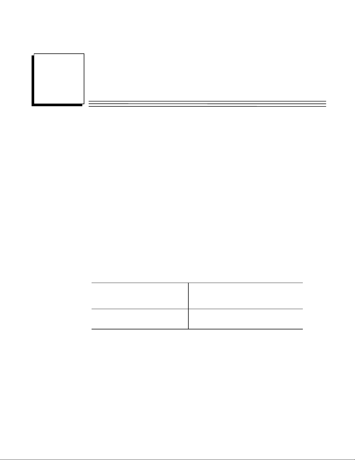
Functional Description
The Analog Output Board internal organization is illustrated in the functional b lock diagram shown
in Figure 1-1 on page 1-4. The board will operate with sustained isolation voltages as high as 1,500
Vpk. Bipolar output voltage ranges are selectable as ±2.5 V, ±5 V, or ±10 V. Unipolar output
voltage ranges are selectable as 0 to 2.5 V, 0 to 5 V, or 0 to 10 V, and full 10 mA loading is
supported throughout these ranges. Four or 8-channel configurations are available.
Voltage outputs may be disconnected under program control during system testing, and are
disconnected automatically during reset. Current-mode outputs support applications that require
standard 4 to 20 mA analog current loops. Compliance of the current mode outputs is 9 V if the
loop supply originate s on the board, or 27 V with an external loop power supply. A front panel
LED (Fail) is provided. The LED is illuminated during power up or system reset and can be turned
OFF under user software control.
1
GFK-2057 Chapter 1 Introduction, Description, and Specifications 1-3
Page 7
or Current Loop Outputs User’s Manual
1
1-4 IC697VAL3xx Series Isolated 4- or 8-Channel 12-bit Analog Output Board with Voltage GFK-2057
OUTPUT CHANNEL 00 (1 OF 8 IDENTICAL CHANNELS)
4-CHANNEL
PTOISOLATOR
O
SHIFT
REGISTER
DATA
1
2
LATCH
1
+5V
DC-TO-DC
– May 2002
CONV
1
2
1
ISOLATED
12-BIT
SERIAL
D/A
VREF
±15 V
RANGE
(VOLTAGE OUTPUT MODULE)
BUFFER
RA NGE
2.5, 5,10 V
(CURRENT OUTPUT MODULE)
OUTPUT
00
VOLTAGE
OR
CURRENT
Figure 1-1: Analog Output Board Functional Block Diagram
E-EXT 00
INTE RNA L
DA TA BUS
VMEb us
P
1
VMEbu s
ATIB
MP
CO
INTE RFACE
CHANNEL
CONTROL
ITY
IL
ISOLATION
BARRIER
ISOLATED
GROUND00
V/I CONV
INT EXT
LOOPSUPPLY
ISOLATED
GROUND-B0
(N/ C)
ISOLAT ED
GROUN D
PLANE
COMM 00
GUARD
+5 V
TO CHANNEL S
01TO 07
Page 8

Safety Summary
The following general safety precautions must be observed during all phases of this
operation, service, and repair of this product. Failure to comply with these precautions or
with specific warnings elsewhere in this manual violates safety standards of design,
manufacture, and intended use of this product. GE Fanuc assumes no liability for the
customer’s failure to comply with these requirements.
Ground the System
To minimize shock hazard, the chassis and system cabinet must be connected to an electrical
ground. A three-conductor AC power cable should be used. The power cable must either be
plugged into an approved three-contact electrical outlet or used with a three-contact to two-contact
adapter with the grounding wire (green) firmly connected to an electrical ground (safety ground) at
the power outlet.
Do Not Operate in an Explosive Atmosphere
1
Do not operate the system in the presence of flammable gases or fumes. Operation of any electrical
system in such an environment constitutes a definite safety hazard.
Keep Away from Live Circuits
Operating personnel must not remove product covers. Component replacement and internal
adjustments must be made by qualified maintenance personnel. Do not replace components with
power cable connected. Under certain conditions, dangerous voltages may exist even with the
power cable removed. To avoid injuries, always disconnect power and discharge circuits before
touching them.
Do Not Service or Adjust Alone
Do not attempt internal service or adjustment unless another person, capable of rendering first aid
and resuscitation, is present.
Do Not Substitute Parts or Modify System
Because of the danger of introducing additional hazards, do not install substitute parts or perform
any unauthorized modification to the product. Return the product to GE Fanuc for service and
repair to ensure that safety features are maintained.
GFK-2057 Chapter 1 Introduction, Description, and Specifications 1-5
Page 9
Chapter
2
Configuration and Installation
This chapter provides configuration and installation instructions for the Relay Board, and is divided
into the following sections:
Ph ysical Installation
Before App lying Power: Checklist
Operational Configuration
Calibration
I/O Cable and Front Connector Configuration
Caution
Some of the components assembled on GE Fanuc products can be sensitive
to electrostatic discharge and damage can occur on boards that are
subjected to a high-energy electrostatic field. When the board is placed on a
bench for configuring, etc., it is suggested that conductive material be placed
under the board to provide a conductive shunt. Unused boards should be
stored in the same protective boxes in which they were shipped.
Upon receipt, any precautions found in the shipping container should be observed. All items should
be carefully unpacked and thoroughly inspected for damage that might have occurred during
shipment. The board(s) should be checked for broken components, damaged printed circuit
board(s), heat damage, and other visible contamination. All claims arising from shipping damage
should be filed with the carrier and a complete report sent to GE Fanuc together with a request for
advice concerning the disposition of the damaged item(s).
GFK-2057 2-1
Page 10

2
Physical Installation
De-energize the equipment and insert the board into an appropriate slot of the chassis. While
ensuring that the board is properly aligned and oriented in the supporting board guides, slide the
board smoothly forward against the mating connector until firmly seated.
Caution
Do not install or remove board while power is applied.
2-2 IC697VAL3xx Series Isolated 4- or 8-Channel 12-bit Analog Output Board with Voltage GFK-2057
or Current Loop Outputs User’s Manual
– May 2002
Page 11

Before Applying Power: Checklist
Before installing the board in a VMEbus system, check the following items to ensure that t he board
is ready for the intended application.
• Have the sections pertaining to and programming and theory, chapters 3 and 4, been
reviewed and applied to system requirements?
• Review “Operational Configuration” on page 2-4 and Table 2-1 on page 2-5 to verify that
all factory-installed jumpers are in place. To change the board address or address modifier
response, refer to “Operational Configuration” on page 2-4.
• Have the I/O cables, with the proper mating connectors, been connected to the
input/output connectors? Refer to “I/O Cable and Front Connector Configuration” on page
2-16 for connector descriptions
• Calibration has been performed at the factory. If recalibration is required, refer to
“Calibration” on page 2-13.
2
After the checklist above has been completed, the b oard can be installed in a VMEbus syste m. This
board may be installed in any slot position, except slot-one which is usually reserved for the system
controller.
Caution
Do not install or remove this board with power applied.
GFK-2057 Chapter 2 Configuration and Installation 2-3
Page 12

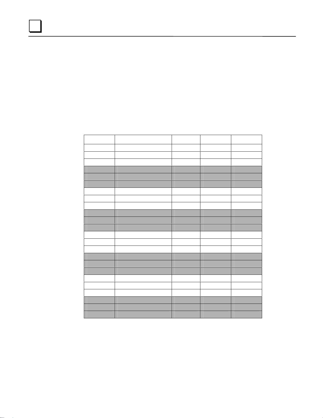
2
Operational Configuration
Control of the Analog Output Board address and I/O access mode are determined by field
replaceable, onboard jumpers. This section describes the use of these jumpers, and their effects onboard performance. The Analog Output Board jumpers are summarized in Table 2-1 on page 2-5.
The locations and functions of all Analog Output Board jumpers are shown in Figure 2-1 on page
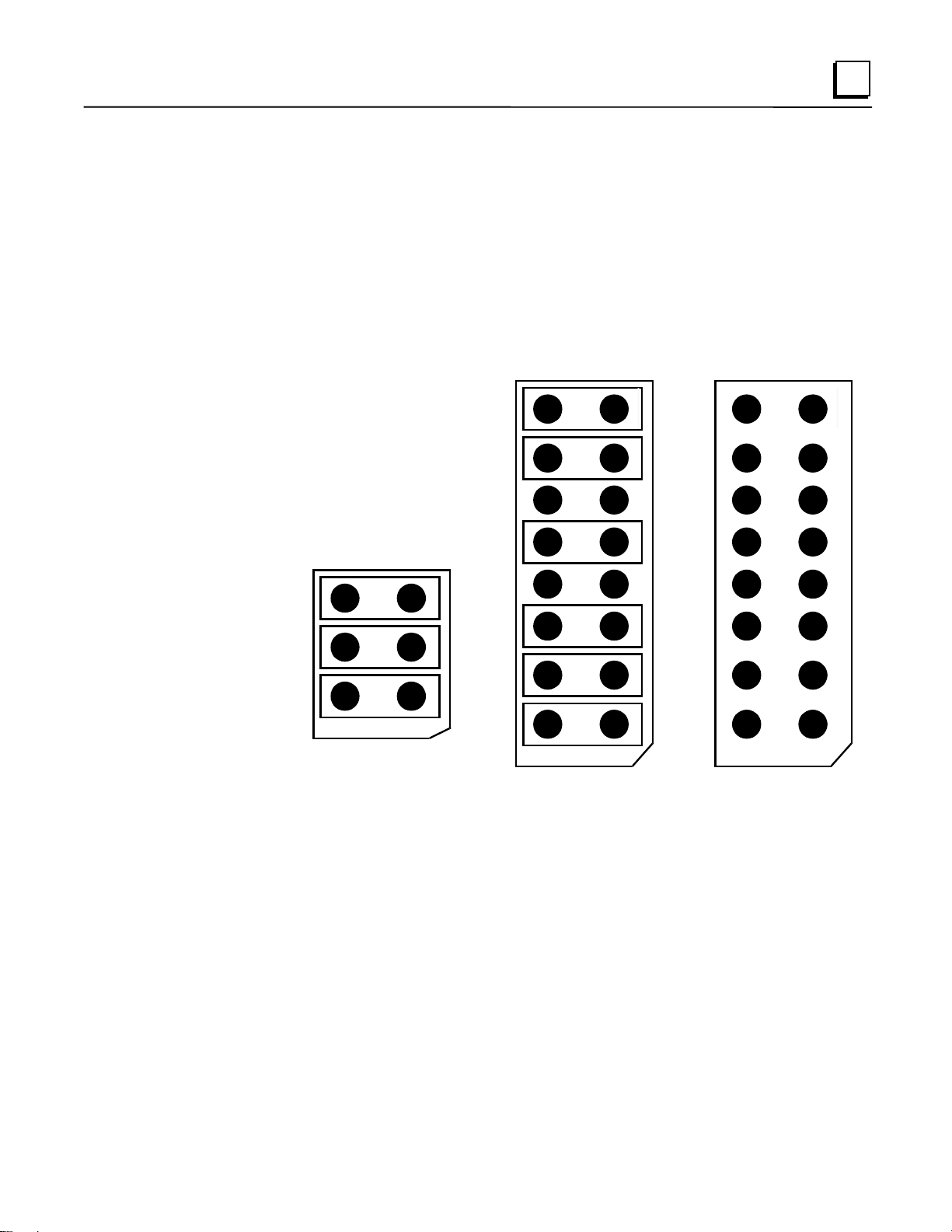
2-6. The function of the output range selec t jumpers are option dependent and will be d iscussed in
detail in “Bipolar Voltage Outputs (Optional)” on page 2-7, “Unipolar Voltage Outputs” on page 28, and “Current Loop Output (Optional)” on page 2-9.
2-4 IC697VAL3xx Series Isolated 4- or 8-Channel 12-bit Analog Output Board with Voltage GFK-2057
or Current Loop Outputs User’s Manual
– May 2002
Page 13

Table 2-1: Analog Output Board Jumper Configuration and Functions
Jumper ID Function Configurable Factory Configuration
E11-1, 2 Supervisory Only Yes Omitted
E11-3, 4 NonprivilegedO nly Yes Installed
E11-5, 6 Short I/O Yes Installed
E12-1, 2 Memory Address Bit A5= 0 Yes Installed
E12-3, 4 Memory Address Bit A6= 0 Yes Installed
E12-5, 6 Memory Address Bit A7= 0 Yes Installed
E9-1, 2 Memory Address Bit A8=0 Yes Installed
E9-3, 4 Memory Address Bit A9=0 Yes Installed
E9-5, 6 Memory Address Bit A10=0 Yes Installed
E9-7, 8 Memory Address Bit A11=0 Yes Installed
E9-9, 10 Memory Address Bit A12=0 Yes Installed
E9-11, 12 Memory Address Bit A13= 0 Yes Installed
E9-13, 14 Memory Address Bit A14= 0 Yes Installed
E9-15, 16 Memory Address Bit A15= 0 Yes Installed
E10-1, 2 Memory Address Bit A16= 0 Yes Installed
E10-3, 4 Memory Address Bit A17= 0 Yes Installed
E10-5, 6 Memory Address Bit A18= 0 Yes Installed
E10-7, 8 Memory Address Bit A19= 0 Yes Installed
E10-9, 10 Memory Address Bit A20= 0 Yes Installed
E10-11, 12 Memory Address Bit A21=0 Yes Installed
E10-13, 14 Memory Address Bit A22=0 Yes Installed
E10-15, 16 Memory Address Bit A23=0 Yes Installed
E1-1, 2 Channel 0 Output Range Sel Yes Installed
E1-2, 3 Channel 0 Output Range Sel Yes Omitted
E2-1, 2 Channel 1 Output Range Sel Yes Installed
E2-2, 3 Channel 1 Output Range Sel Yes Omitted
E3-1, 2 Channel 2 Output Range Sel Yes Installed
E3-2, 3 Channel 2 Output Range Sel Yes Omitted
E4-1, 2 Channel 3 Output Range Sel Yes Installed
E4-2, 3 Channel 3 Output Range Sel Yes Omitted
E5-1, 2 Channel 4 Output Range Sel Yes *Installed
E5-2, 3 Channel 4 Output Range Sel Yes Omitted
E6-1, 2 Channel 5 Output Range Sel Yes *Installed
E6-2, 3 Channel 5 Output Range Sel Yes Omitted
E7-1, 2 Channel 6 Output Range Sel Yes *Installed
E7-2, 3 Channel 6 Output Range Sel Yes Omitted
E8-1, 2 Channel 7 Output Range Sel Yes *Installed
E8-2, 3 Channel 7 Output Range Sel Yes Omitted
2
* Omitted for 4-Channel Op tions
GFK-2057 Chapter 2 Configuration and Installation 2-5
Page 14

2
U16
U16
Figure 2-1: Location of User-Configurable Jumpers and Potentiometers
6
1
R
U12
U10
1
D
U8
2
2
2
3
3
3
C
A
B
U15
8
E
4
1
R
7
E
2
1
R
6
E
0
1
R
5
E
8
R
4
E
6
R
3
E
U10*
U8*
U15*
*
*
*
1
1
1
C
B
A
P1
0
1
E
9
E
2
2
2
3
3
3
C
B
A
2
1
E
1
1
E
1
1
1
C
B
A
U14
4
R
2
E
2
R
1
E
*
*
P2
2
2
2
3
3
3
C
B
A
– May 2002
P3
2
2
2
A
B
C
* Potentiometers are located in this position on the current output
board only.
2-6 IC697VAL3xx Series Isolated 4- or 8-Channel 12-bit Analog Output Board with Voltage GFK-2057
or Current Loop Outputs User’s Manual
Page 15

Bipolar Voltage Outputs (Optional)
The following table applies to IC697VAL304 and IC697VAL308 only.
The Analog Output Board provides Bipola r Voltage Outputs for four or eight channels. The
channel can be configured by user-installed jumpers for ±2.5 V, ±5 V, or ±10 V. Table 2-2 below
describes the jumper functions for this mode, along with the designators for the adjustment
potentiometers (POT) associated with each channel.
Table 2-2: Bipolar Voltage Jumper Functions
Channel* Output Range Jumper Voltage Gain Adj Zero Adj
0 E1-1,2 ±2.5 V R2 U1 POT
0 E1-2,3 ±5 V R2 U1 POT
0 E1-OPEN ±10 V R2 U1 POT
1 E2-1,2 ±2.5 V R4 U14 POT
1 E2-2,3 ±5 V R4 U14 POT
1 E2-OPEN ±10 V R4 U14 POT
2 E3-1,2 ±2.5 V R6 U15 POT
2 E3-2,3 ±5 V R6 U15 POT
2 E3-OPEN ±10 V R6 U15 POT
3 E4-1,2 ±2.5 V R8 U16 POT
3 E4-2,3 ±5 V R8 U16 POT
3 E4-OPEN ±10 V R8 U16 POT
4 E5-1,2 ±2.5 V R10 U6 POT
4 E5-2,3 ±5 V R10 U6 POT
4 E5-OPEN ±10 V R10 U6 POT
5 E6-1,2 ±2.5 V R12 U8 POT
5 E6-2,3 ±5 V R12 U8 POT
5 E6-OPEN ±10 V R12 U8 POT
6 E7-1,2 ±2.5 V R14 U10 POT
6 E7-2,3 ±5.0 V R14 U10 POT
6 E7-OPEN ±10 V R14 U10 POT
7 E8-1,2 ±2.5 V R16 U12 POT
7 E8-2,3 ±5 V R16 U12 POT
7 E8-OPEN ±10 V R16 U12 POT
* Channels 0 through 3, the IC697VAL304 option of the Analog Output Board
Channels 0 through 7, the IC697VAL308 option of the Analog Output Board
2
Note
GFK-2057 Chapter 2 Configuration and Installation 2-7
Page 16
2
Unipolar Voltage Outputs (Optional)
The following table applies to IC697VAL324 and IC697VAL328 only.
The Analog Output Board provides Unipolar Voltage outputs for four or eight channels. The
channel can be configured by way of user-installed jumpers for 0 to 2.5 V, 0 to 5 V, or 0 to 10 V.
Table 2-3 below describes the jumper functions for this mode, along with the associated gain and
zero adjustment designator for each channel.
Table 2-3: Unipolar Voltage Jumper Functions
Channel* Output Range Jumper Voltage Gain Adj Zero Adj
0 E1-1,2 0 to 2.5 V R2 U1 POT
0 E1-2,3 0 to 5 V R2 U1 POT
0 E1-OPEN 0 to 10 V R2 U1 POT
1 E2-1,2 0 to 2.5 V R4 U14 POT
1 E2-2,3 0 to 5 V R4 U14 POT
1 E2-OPEN 0 to 10 V R4 U14 POT
2 E3-1,2 0 to 2.5 V R6 U15 POT
2 E3-2,3 0 to 5 V R6 U15 POT
2 E3-OPEN 0 to 10 V R6 U15 POT
3 E4-1,2 0 to 2.5 V R8 U16 POT
3 E4-2,3 0 to 5 V R8 U16 POT
3 E4-OPEN 0 to 10 V R8 U16 POT
4 E5-1,2 0 to 2.5 V R10 U6 POT
4 E5-2,3 0 to 5 V R10 U6 POT
4 E5-OPEN 0 to 10 V R10 U6 POT
5 E6-1,2 0 to 2.5 V R12 U8 POT
5 E6-2,3 0 to 5 V R12 U8 POT
5 E6-OPEN 0 to 10 V R12 U8 POT
6 E7-1,2 0 to 2.5 V R14 U10 POT
6 E7-2,3 0 to 5 V R14 U10 POT
6 E7-OPEN 0 to 10 V R14 U10 POT
7 E8-1,2 0 to 2.5 V R16 U12 POT
7 E8-2,3 0 to 5 V R16 U12 POT
7 E8-OPEN 0 to 10 V R16 U12 POT
* Channels 0 Through 3, the IC697VAL324 option of the Analog Output Board
Channels 0 Through 7, the IC697VAL328 option of the Analog Output Board
Note
2-8 IC697VAL3xx Series Isolated 4- or 8-Channel 12-bit Analog Output Board with Voltage GFK-2057
or Current Loop Outputs User’s Manual
– May 2002
Page 17

Current Loop Output (Optional)
The following table applies to IC697VAL314 and IC697VAL318 only.
The Analog Output Board provides Current Loop Outputs for four or eight channels. A 15 V loop
power supply is provided on the board, or a maximum of 30 V can be supplied with an external
loop power supply. A jumper is provided fo r each channel to configure the internal or external
power supply as shown in Table 2-4 below.
Table 2-4: Current Loop Output Jumper Functions
Channel* Jumper Loop Supply Gain Adj Zero Adj
0 E1-1,2 Internal R2 U1 POT
0 E1-2,3 External R2 U1 POT
1 E2-1,2 Internal R4 U14 POT
1 E2-2,3 External R4 U14 POT
2 E3-1,2 Internal R6 U15 POT
2 E3-2,3 External R6 U15 POT
3 E4-1,2 Internal R8 U16 POT
3 E4-2,3 External R8 U16 POT
4 E5-1,2 Internal R10 U6 POT
4 E5-2,3 External R10 U6 POT
5 E6-1,2 Internal R12 U8 POT
5 E6-2,3 External R12 U8 POT
6 E7-1,2 Internal R14 U10 POT
6 E7-2,3 External R14 U10 POT
7 E8-1,2 Internal R16 U12 POT
7 E8-2,3 External R16 U12 POT
* Channels 0 Through 3, the IC697VAL314 option of the Analog Output Board
Channels 0 Through 7, the IC697VAL318 option of the Analog Output Board
2
Note
GFK-2057 Chapter 2 Configuration and Installation 2-9
Page 18

2
Figure 2-2: Typical External Voltage Connection
OUTPUT
MODULE
P3
+15V
OUT
AGND
VLOOP
321
EXTERNAL
OUT
COMM
-
VEXT
+
LOAD
EXTERNAL
VOLTAGE
SOURCE
30 VOLTS MAX
2-10 IC697VAL3xx Series Isolated 4- or 8-Channel 12-bit Analog Output Board with Voltage GFK-2057
or Current Loop Outputs User’s Manual
– May 2002
Page 19

Address Modifiers
The Analog Output Board is factory configured to respond to short nonprivileged access as shown
in Figure 2-3 below and Figure 2-4 on page 2-12. The configuration can be changed by installing
jumpers at the appropriate locations in the header as shown in Figure 2-3 below and Figure 2-4 on
page 2-12.
2
Figure 2-3: Address Modifier Jumper Configurations (a)
E11
E11
Short
I/O
Short
I/O
NP
NP
Supervisory
1
Jumper Configuration for Standard
Supervisory Access
Supervisory
1
Jumper Configuration for Shor t
Addressing with Supervisory or
Nonprivileged Access
Short
I/O
NP
Supervisory
1
Jumper Configuration for Standard
Addressing with Supervisory or
E11
GFK-2057 Chapter 2 Configuration and Installation 2-11
Nonprivileged Access
Page 20

2
Figure 2-4: Address Modifier Jumper Configurations (b)
E11
E11
Short
I/O
Short
I/O
NP
NP
Supervisory
1
Jumper Configuration for Shor t
Supervisory Access
Supervisory
1
Jumper Configuration for Standard
Nonprivileged Access
E11
Short
I/O
NP
Supervisory
1
Jumper Configuration for Shor t
Nonprivileged Access
2-12 IC697VAL3xx Series Isolated 4- or 8-Channel 12-bit Analog Output Board with Voltage GFK-2057
or Current Loop Outputs User’s Manual
– May 2002
Page 21
Address Selection
The Analog Output Board is designed with banks of Address Select Jumpers that specify the base
address of the board. The Address Selection Jumpers are shown in Figure 2-5 below. The Analog
Output Board is factory configured to respond to $0000 short nonprivileged access. An installed
jumper causes the board to compare to a low address line, an omitted jumper causes the board to
compare to a high address line.
2
Figure 2-5: Base Address Select Jumpers
E12
A15
A14
A13
A12
A11
E9
A23
A22
A21
A20
A19
E10
A07
A10
A18
A06
A09
A17
A05
A08
The example shown is for a I/O base address of $2800h (Short I/O Access) or FF2800 (Standard
I/O Access)
A16
GFK-2057 Chapter 2 Configuration and Installation 2-13
Page 22

2
Calibration
Before delivery from the factory, the Analog Output Board is fully calibrated. Should recalibration
be required, refer to “Equipment Required” and “Analog Outputs Calibration Procedure” below,
“Bipolar Voltage Output Cali bration” and “Unipolar Voltage Output Calibration” on page 2-14,
and “Current Output Calibration” on page 2-15 and perform the indicated calibration procedures in
the order shown. Location of all adjustments are shown in Figure 2-1 on page 2-6. As delivered
from the factory, all calibration adjustments are sealed against accidental movement. The seals are
easily broken for recalibration, however, all adjustments should be resealed with a suitable fastcuring sealing compound after recalibration has been completed.
Note:
The bipolar and unipolar voltage modules (option dependent) will be
calibrated at full scale value for the MINimum range. If the user configures
the board for any OTHER range, calibration will be required.
Equipment Required
Digital Mutimeter:
Chassis:
Extender Card:
Resistors:
Voltage Measurements: ±10 VDC range; 5 or more digits; ±0.005 percent
of reading accuracy; 10W minimum input resistance.
Current Measurements: 0 -100 mADC range; 5 or more digits; ±0.005
percent of reading accuracy; 100 maximum input resistance.
VMEbus 6U backplane or equivalent, with J1 and J2 connectors, 680x0
series controller, +5 ±0.2 VDC, 8 Amp (reserved current) power supply.
One slot allocated for testing the Analog Output Board.
VMEbus 6U extender card.
250Ω ±5%, 1/4 watt (current outputs only)
Analog Outputs Calibration Procedure
1. Refer to “Operational Configuration” on page 2-4 and configure the Analog Output Board
for the output configuration that is required for the application. For calibration of current
outputs, configure the outputs for operation with the internal loop supply.
2. Install the Analog Output Board on an extender card in the VMEbus chassis. Make
provisions for connecting the DMM to each analog output channel, with the (+) common
lead at the output pin (OUT*) and the (-) lead at the common pin (COMM*). The channel
output pins are defined in the table in Figure 2-6 on page 2-16.
3. Apply power to the board. Write the value A000 (HEX) to the CSR, this will enable all
outputs and extinguish the fail LED (refer to Table 3-1 on page 3-2 for the locations of all
registers). All data transfers will be D16.
4. Allow a minimum warm-up interval of ten minutes before proceeding.
2-14 IC697VAL3xx Series Isolated 4- or 8-Channel 12-bit Analog Output Board with Voltage GFK-2057
or Current Loop Outputs User’s Manual
– May 2002
Page 23

5. See the following sections for bipolar voltage outputs, unipolar voltage outputs, or current
outputs. The locations of output modules and adjustment potentiometers are illustrated in
Figure 2-1 on page 2-6.
Bipolar Voltage Output Calibration
1. Connect the DMM to the channel 00 output pins, with the (+) lead connected to the output
pin and the (-) lead connected to the common pin.
2. Write the value $0800 to the channel 00 output data register. Adjust the ZERO
potentiometer on the channel 00 output module for a DMM indication that conforms to the
MIDSCALE value contained in Table 2-5 below for the assigned output range.
3. Write the value $0FFF to the c han nel 00 output data register. Adjust the Channel-00 gain
potentiometer for a DMM indication that conforms to the POSITIVE FULL SCALE value
contained in Table 2-5 below for the assigned output range.
4. Write the value $0000 to the channel 00 output data register. If the DMM indication does
not conform to the NEGATIVE FULL SCALE value co ntained in Table 2-5 below for the
assigned output range, repeat steps 2, 3, and 4 until the measurements for all three steps
are correct.
2
5. Repeat steps 1 through 4 for the remaining active output channels.
6. Bipolar calibration is completed. Remove power. Remove all test connections.
Table 2-5: Bipolar Voltage Output Calibration Values
Output Range
(VDC)
±2.5 0.0000 ±0.0006 +2.4988 ±0.0006 -2.5000 ±0.008
±5 0.0000 ±0.0010 +4.9975 ±0.0010 -5.0000 ±0.011
±10 0.0000 ±0.0002 +9.9951 ±0.0020 -10.0000 ±0.018
Midscale
Output Value (VDC)
Unipolar Voltage Output Calibration
1. Connect the DMM to the channel 00 output pins, with the (+) lead connected to the output
pin and the (-) lead connected to the common pin.
2. Write the value $0000 to the channel 00 output data register. Adjust the channel 00 gain
potentiometer for a DMM indication that conforms to the ZERO value contained in Table
2-6 on page 2-15 for the assigned output range.
3. Write the value $0FFF to the channel 00 output data register. If the DMM indication does
not conform to the POSITIVE FULL SCALE value contained in Table 2-6 on page 2-15
for the assigned output range, repeat steps 2, 3, and 4 until the measurements for all three
steps are correct.
Positive Full
Scale
Negative Full
Scale
4. Repeat steps 1 through 3 for the remaining active output channels.
5. Unipolar calibration is completed. Remove power. Remove all test connections.
GFK-2057 Chapter 2 Configuration and Installation 2-15
Page 24

2
Table 2-6: Unipolar Voltage Output Calibration Values
Output Range
(VDC)
0 to +2.5 0.0000 ±0.0006 +2.4988 ±0.0015
0 to +5 0.0000 ±0.0010 +4.9975 ±0.0020
0 to +10 0.0000 ±0.0020 +9.9951 ±0.0040
Zero Positive Full Scale
Current Output Calibration
1. Connect the DMM to the channel 00 output pins (see the table in Figure 2-6 on page 2-
16), with the (+) lead connected to the output pin through a series resistance of 250, and
the (-) lead connected to the common pin. Leave the external loop supply pins (VEXT)
disconnected.
2. Write the value $0000 to the channel 00 output data register. Adjust the ZERO
potentiometer on the channel 00 output module for a DMM indication that conforms to the
ZERO SCALE value contained in Table 2-7 below for the assigned output range.
3. Write the value $0FFF to the c han nel 00 output data register. Adjust the cha nnel 00 gain
potentiometer for a DMM indication that conforms to the FULL SCALE value contained
in Table 2-7 below for the assigned output range.
4. Repeat steps 1 through 4 for the remaining active output channels.
5. Calibration is completed. Remove power, remove all test connections.
Output Value (VDC)
Table 2-7: Current Output Calibration Values
Output Range
(mADC)
4 to 20 4.000 ±0.004 +20.000 ±0.008
Output Value (mADC)
Zero Positive Full Scale
2-16 IC697VAL3xx Series Isolated 4- or 8-Channel 12-bit Analog Output Board with Voltage GFK-2057
or Current Loop Outputs User’s Manual
– May 2002
Page 25
I/O Cable and Front Connector Configuration
The front input connector (P3) on the Analog Output Board is a standard 41612 DIN form E screw
terminal connector. The P3 connector pin layout is shown in Figure 2-6 below. The pin
assignments for P3 are also shown below. The connector is supplied with integral latches. To
remove the connector, depress both latches simultaneously while gently pulling connector from
socket. Install connector by aligning keying and pressing the connector into place.
32-Pin DIN Connector: Connector Specification
• Wire should be 14-22 AWG
• Insulation stripping length: .315” ±.20”/8mm ±0.5mm
• The binding screw terminals are best suited for a .138” x.20”/3.5mm x 0.5mm common
flat-blade screwdriver.
2
• Recommended screw tightening torque: 5 . 22 lb./in. /0.6mN
• Contact resistance: <
Due to chassis vibration, GE Fanuc recommends periodic checks of screw
torque.
Front View (Cable Side) of
P3 Connector
PIN No.
A32
A2
C2
C32
10 mΩ
Note
Figure 2-6: P3 Connector Pin Layout and P3 Pin Assignments
P3 Pin No. Signal P3 Pin No. Signal
A32 *VEXT 7 C32 N/C
A30 OUT 7 C30 COMM 7
A28 *VEXT 6 C28 N/C
A26 OUT 6 C26 COMM 6
A24 *VEXT 5 C24 N/C
A22 OUT 5 C22 COMM 5
A20 *VEXT 4 C20 N/C
A18 OUT 4 C18 COMM 4
A16 *VEXT 3 C16 N/C
A14 OUT 3 C14 COMM 3
A12 *VEXT 2 C12 N/C
A10 OUT 2 C10 COMM 2
A8 *VEXT 1 C8 N/C
A6 OUT 1 C6 COMM 1
A4 *VEXT 0 C4 N/C
A2 OUT 0 C2 COMM 0
* VEXT pins have no effect on voltage outputs.
GFK-2057 Chapter 2 Configuration and Installation 2-17
Page 26

Chapter
3
Programming
This chapter contains programming instructions for the Relay Board , and is divided into the
following sections:
Introduction to Controlling the Analog Output Board
Board Identification Register (BIR)
Contro l/Status Register (CSR)
Control of Analog Outputs
Reset Operatio ns
GFK-2057 3-1
Page 27

3
Introduction to Controlling the Analog Output Board
Communication with the Analog Output Board is established through control, status, data, and
identification registers that are mapped into a 16-word block. On-board configurable address
jumpers permit the communication registers to be located in either the A16 short or the A24
standard I/O data space. Access privilege is jumper-selectable as supervisory, nonprivileged, or
both. All registers are listed in Table 3-1 below and described throughout this section.
Each of the eight analog outputs is controlled through a dedicated 12-bit Output Data Register
(ODR). Data is serialized and transferred to an output D/A converter when the associated ODR
receives a data transfer from the bus. All channels operate independently.
All read/write registers are cleared to ZERO by a system reset or power up operation. The reset
operation places the board in the following state:
Analog Output Level Current and voltage outputs are at lowest level.
Analog Output State All voltage channels are disconnected from the output connectors, no
effect on current option.
Data Coding Offset binary.
Front Panel LED Illuminated.
Table 3-1: Analog Output Board Register Map
Board Address
(Hex)
00 Board ID BIR Read Only Byte/Word/Longword
04 Control and Status CSR Read/Write Byte/Word
06 Reserved ... ...
08 CH 00 Output Data ODR 00 Read/Write Word
0A CH 01 Output Data ODR 01 Read/Write Word
0C CH 02 Output Data ODR 02 Read/Write Word
0E CH 03 Output Data ODR 03 Read/Write Word
10 CH 04 Output Data ODR 04 Read/Write Word
12 CH 05 Output Data ODR 05 Read/Write Word
14 CH 06 Output Data ODR 06 Read/Write Word
16 CH 07 Output Data ODR 07 Read/Write Word
18 to 1E Reserved ... ...
Register
Function
Description Access Size
3-2 IC697VAL3xx Series Isolated 4- or 8-Channel 12-bit Analog Output Board with Voltage GFK-2057
or Current Loop Outputs User’s Manual
– May 2002
Page 28
Board Identification Register (BIR)
The Board Identification register contains the board identification code ($46000000) for the Analog
Output Board, and occupies the first two words at the board base address.
Table 3-2: Board ID Register Bit Map
Board ID Register (Offset Address $00) Read-only, Byte
Bit 15 Bit 14 Bit 13 Bit 12 Bit 11 Bit 10 Bit 09 Bit 08
0 1 0 0 0 1 1 0
Board ID Register (Offset Address $00) Read-only, Byte
Bit 07 Bit 06 Bit 05 Bit 04 Bit 03 Bit 02 Bit 01 Bit 00
0 0 0 0 0 0 0 0
3
GFK-2057 Chapter 3 Programming 3-3
Page 29

3
Control/Status Register (CSR)
Control/Status register functions and the bitmap are summarized in Table 3-3 below. Control
register bits are mapped directly to the readback STATUS register at the same location. All CSR
bits are cleared to zero (LOW) during a power up or reset operation. The CSR provides control and
monitoring of the following board functions:
• Output enabling (voltage outputs)
• Output load cycle status
• Data coding
• Self test LED
Table 3-3: Analog Output Board Control/Status Register (CSR) Bit Map
CSR (Offset Address $04) Read/Write, Byte/Word
Bit 15 Bit 14 Bit 13 Bit 12 Bit 11 Bit 10 Bit 09 Bit 08
LED Reserved
Bit 07 Bit 06 Bit 05 Bit 04 Bit 03 Bit 02 Bit 01 Bit 00
CH 7
Busy
CH 6
Busy
Output
EN
CSR (Offset Address $04) Read/Write, Byte/Word
CH 5
Busy
Two’s
CMPL
CH 4
Busy
Control/Status Register Bit Definitions
Bit 15: LED – The "FAIL LED" is OFF if Bit 15 is set (logical "1"), or is ON if bit
is cleared (logical "0"). Default = logical "0".
Bit 14: Reserved – This bit is reserved and forced to a logical "0".
Bit 13: Output Enable – Output Enable: All outputs are connected to the output
connectors if Bit 13 is set to a logical "1," or disconnected if Bit 13 is
cleared to a logical zero.
Bit 13 has no effect on current outputs. Default = logical "0."
Note
CH 3
Busy
Reserved
CH 2
Busy
CH 1
Busy
CH 0
Busy
For current output options, the outputs are placed in a minimal current
output state when this bit is cleared to a zero. This bit must be set to a "1" to
allow operation. For the default state, reference “Reset Operations” on page
3-8.
3-4 IC697VAL3xx Series Isolated 4- or 8-Channel 12-bit Analog Output Board with Voltage GFK-2057
or Current Loop Outputs User’s Manual
– May 2002
Page 30

3
Bit 12: Two’s Complement – Channel data is processed in 12-bit offset binary if
Bit 12 is cleared (reset default) or in two’s complement format with
extended sign if Bit 12 is set a logical "1".
Bits 11 through 08: Reserved – This bit is reserved and forced to a logical "0".
Bits 07 through 00: CH Busy – The Channel Busy flag is set when the associated channel
Output Data Register receives a data transfer from the bus, and remains set
for approximately 8 msec while the data word is transferred to the output
D/A converte r. A channel register should not be updated from the bus
while the associated busy flag is set.
Note
LOGIC STATE CONVENTION – To avoid ambiguities in references to
logic levels, this document uses the convention that a data bit or control line
is "SET" when it is in the "1", or HIGH state, and is "CLEARED" when
"0" or LOW STATE.
GFK-2057 Chapter 3 Programming 3-5
Page 31

3
Control of Analog Outputs
Output Registers and Data Format
The eight independent analog outputs are controlled through output data registers ODR 00 through
ODR 07. Readback capability is provided, and both D8 (even/odd) and D16 transfers are
supported. It is advisable to update data registers in word format. Data is configured in rightjustified 12-bit offset binary format or two’s complement format, data format is controlled by CSR
Bit 12.
In the offset binary format (reset default), the upper four bits D12 to D15 are ignored during
loading and are returned as zero during readback. In two’s complement format, data is received and
returned in two’s complement with the sign extended through the most significant bit, Bit 15 during
readback.
Table 3-4: Bipolar Output Offset Binary Format Bit Map
Bipolar Output Data Register Read/Write, Byte/Word
Bit 15 Bit 14 Bit 13 Bit 12 Bit 11 Bit 10 Bit 09 Bit 08
X X X X D11 D10 D09 D08
Bipolar Output Data Register Read/Write, Byte/Word
Bit 07 Bit 06 Bit 05 Bit 04 Bit 03 Bit 02 Bit 01 Bit 00
D07 D06 D05 D04 D03 D02 D01 D00
Table 3-5: Bipolar Output Data Register Bit Map (Two’s Complement)
Bipolar Output Data Register Read/Write, Byte/Word
Bit 15 Bit 14 Bit 13 Bit 12 Bit 11 Bit 10 Bit 09 Bit 08
X X X X D11 D10 D09 D08
Bipolar Output Data Register Read/Write, Byte/Word
Bit 07 Bit 06 Bit 05 Bit 04 Bit 03 Bit 02 Bit 01 Bit 00
D07 D06 D05 D04 D03 D02 D01 D00
3-6 IC697VAL3xx Series Isolated 4- or 8-Channel 12-bit Analog Output Board with Voltage GFK-2057
or Current Loop Outputs User’s Manual
– May 2002
Page 32
Table 3-6: Data Codes for Some Selected Output Voltages
3
Offset
Binary
000 800 -10 V +0 V - FSR
400 C00 -5 V + 2.5 V 1/4 FSR
800 000 +0 V +5 V 1/2 FSR
C00 400 +5 V +7.5 V 3/4 FSR
FFF 7FF +9.9951 V +9.9951 V + FSR - 1 LSB
Two’s
Comp
Scaling and Enabling
Available output ranges are ±2.5 V, ±5 V, or ±10 V for bipolar voltage outputs, 0 to +2.5 V, 0 to
+5 V, or 0 to +10 V for unipolar voltage outputs, and 4 to 20 mA for current outputs. The analog
output range is determined independently for each output channel by on-board jumpers which are
described in Chapter 2. All voltage outputs are disconnected from the output connectors if Bit 13 in
the CSR is cleared, or connected to the output connectors if CSR Bit 13 is set.
If the CSR Bit 12 control bit is cleared, the output data is coded in offset binary. Each output level
is scaled linearly from $0000 for negative full scale or lowest output level, to $0FFF for positive
full scale, or highest output level.
For two's complement coding (CSR Bit 12 set), the output data is scaled from $F800 for negative
full scale to $07FF for positive full scale. Two's complement co ding normally is used only for
bipolar outputs. Various coding examples are summarized in Table 3-6 above.
Bipolar
Output ±10 V
Unipolar Output
0 - 10 V
Scale Factor
Output Load Cycles
Data from an output data register is transferred serially to the output D/A converter during an
internal Output Load Cycle. A data transfer to a data register initiates a load cycle for the
associated output channel. The load cycle is completed in approximately 8 msec, and proceeds
automatically after initiation without further interve ntion from the VMEbus. The level of the
associated analog output channel is updated at the end of the load cycle. For D8 transfers, the load
cycle is initiated by an odd-byte transfer.
Each Channel Busy Flag (Bit 00 through B it 07) is set when the assigned channel output data
register receives a data transfer from the bus, and remains set for approximately 8 msec during the
ensuing output load cycle. Data transfers to an output register should not take place while the
associated busy flag is set. However, any register can be read at any time without affecting board
performance. All output channels are controlled independently, and any output data register can be
updated without affecting the other seven chan nels.
GFK-2057 Chapter 3 Programming 3-7
Page 33

3
Reset Operations
All read/write registers are cleared to ZERO by a system reset operation. The reset operation places
the board in the following state:
Analog Output Level For options "-AB1," current outputs are minimal; For options "-AB0,"
Analog Output State All voltage channels are disconnected from the output connectors.
Data Coding Offset binary.
Front Panel LED Illuminated.
current outputs are on-line and full-scale voltage outputs are minus full
scale.
3-8 IC697VAL3xx Series Isolated 4- or 8-Channel 12-bit Analog Output Board with Voltage GFK-2057
or Current Loop Outputs User’s Manual
– May 2002
Page 34

Chapter
4
Theory of Operation
This chapter describes the internal organization of the Analog Output Board, reviews the general
principles of operation, and is d ivided into the following sections:
Internal Functional Organization
VMEbus Interface
Channel Control Logic
Analog Output Channels
DC/D C Power Converters
GFK-2057 4-1
Page 35

4
Internal Functional Organization
Optical data coupling, serial data transfers, and isolated Digital-to-Analog Converters (DACs) are
used to produce eight galvanically isolated analog output channels. Each channel contains a serial
12-bit DAC which generates a sig nal voltage in response to commands from the VMEbus. The
DAC voltage then drives an output module which is factory configured for a specific voltage or
current output option. Power for each channel is supplied as ±15 VDC by an isolated DC-to-DC
converter. A functional block diagram of the Analog Output Board is shown in Figure 1-1 on page
1-4.
The Analog Output Board consists of the following functional elements, all of which are describ ed
in the following sections:
• VMEbus interface
• Channel control logic
• Isolated analog outputs
• DC/DC power converters
4-2 IC697VAL3xx Series Isolated 4- or 8-Channel 12-bit Analog Output Board with Voltage GFK-2057
or Current Loop Outputs User’s Manual
– May 2002
Page 36

VMEbus Interface
Communications with the VMEbus is controlled with a single Electrically Programmable Logic
Device (EPLD), as shown in Figure 4-1 on page 4-4. Data and control registers are distributed
among two channel-control EPLD’s. The control-logic EPLD responds to data transfer requests
from the VMEbus, and directs the flow of data between the bus and the internal data and control
registers. Data Transfer Acknowledge (DTACK*) is generated when a transfer from the bus has
been completed, or when data is ready to be transferred to the bus. Transfers proceed normally if
address pipelining is present, but the board will respond only to the first address in the pipeline
sequence. The VMEbus interface logic will not respond to transfer requests in which the BERR*,
DTACK*, LWORD*, or IACK* control line is asserted.
4
GFK-2057 Chapter 4 Theory of Operation 4-3
Page 37

4
Channel Control Logic
Control of data transfer to the output DAC is partitioned into two identical 4-channel groups, with a
single EPLD assigned to each group. This method of partitioning permits the board to be populated
with only those devices required to support the 4- or 8-channel optional configuration.
As shown in Fi gure 4-1 below , the EPLD which c ontrols channe ls 00 through 0 3 also contains the
Board Identification Register (BIR) and part of the Control/Status register (CSR). This EPLD
detects the presence of one or both of the channel-control EPLD, and adjusts the distribution of the
CSR accordingly.
Figure 4-1: VMEbus Interface and Control
CHANNELS 00-03 CONTROL
ID00-15
XCVR
VMEbus
P1
VMEbus
BUFFERS
CONTROL
LOGIC
(EPLD)
INTERNAL
DATA
INTERNAL
CONTROL
ID00-15
R/W
REG ADDR
R/W
CSR D00-03
D12-15
BIR D00-D31
MUX
CHANNELS 04-07 CONTROL
XCVR
MUX
CHANNEL 00
CONTROL
CHANNEL 01
CHANNEL 02
CHANNEL 03
CSR D04-07
CHANNEL 04
CONTROL
CHANNEL 05
CHANNEL 06
CHANNEL 07
ENABLE OUTPUTS
DTA, CLK, LD
GROUP 1,2
PRESENT
DTA, CLK, LD
TO
OPTICAL
COUPLERS
REG ADDR
4-4 IC697VAL3xx Series Isolated 4- or 8-Channel 12-bit Analog Output Board with Voltage GFK-2057
or Current Loop Outputs User’s Manual
– May 2002
Page 38

4
Each channel-control EPLD contains four data registers which receive the channel data words from
the VMEbus, and provides an independent data serializer for each channel. Figure 4-2 on page 4-7
illustrates the movement of data within a single control channel. A data transfer to any 16-bit
channel data register from the bus initiates t he serializing process which moves the data to the
serial output D/A converter. Data in each register is right-justified with 12 significant bits.
Only the 12 significant data bits in each channel are serialized for transfer to the associated D/A
converter. The four digital signals required to produce the transfer are shown in Figure 4-3 on page
4-8. The board selection (BDSEL L) initiates the transfer sequence. The CLOCK line provides the
primary timing, and clocks the information present on the DATA line into the serial D/A converter,
MSB first through LSB last. The output of the converter does not change during the serial transfer.
When the serial transfer has been completed, the LOAD signal performs a parallel transfer of data
to an output latch in the conver ter, and the output voltage responds to the new data.
GFK-2057 Chapter 4 Theory of Operation 4-5
Page 39

4
Analog Output Channels
Isolation
Each output channel is isolated from the VMEbus and from all other channels by an isolated
DC/DC converter and by four optical couplers. The DC/DC converter provides isolated ±15 VDC
power for the channel, and the optical couplers isolate the digital control signals IDTA, ICLK, ILD,
and IENA from EPLD signals DATA, CLOCK, LOAD, and ENAOUT (Figure 4-4 on page 4-9).
Power for the optical couplers is supplied as +5 VDC, and is series regulated from the isolated +15
V rail.
Digital-to-Analog Conversion
A serial Digital-to-Analog Converter (DAC) receives the 12-bit data word from the channel control
EPLD, and produces an output voltage range that is jumper controlled from 0 to 10 V. The D/A
buffer converts this range into the output ranges specified in the output ordering option. Ch annel
span is adjusted in the feedback loop of the D/A buffer.
The voltage reference level is selected as +2.5 V, +5 V, or +10 V by the output module. A current
output module automatically selects a +10 V reference. A voltage output module passes the state of
the module control jumpers directly to the reference, and permits any of the three voltages to be
selected.
4-6 IC697VAL3xx Series Isolated 4- or 8-Channel 12-bit Analog Output Board with Voltage GFK-2057
or Current Loop Outputs User’s Manual
– May 2002
Page 40

IDB00-15
RD DTA H
4
Figure 4-2: Analog Output Board Channel Control
CHANNEL CONTROL EPLD
BUS XCVR
16
REG ADDR A1-A4 H
WR DT A H
CLK4 H
CLK8 H
4
12
SEQUENCE
CONTROL
DATA
REGISTER
CHANNEL
MULTIPLEXER
CT RXX 0-3
4
COUNTER
4 CHANNELS
DT AXX H
TO OPTICAL
COUPLERS
CLKXX H
LDXX L
ONE OF
GFK-2057 Chapter 4 Theory of Operation 4-7
Page 41

4
BD SEL L
DATA
Figure 4-3: Analog Output Board Output Timing (Typical Channel)
µ
8.5
SEC MAX
DB 11 (MSB)
CLOCK (2 MHz)
LOAD
Voltage and Current Outputs
All outputs are factory-configured for either unipolar voltage, bipolar voltage, or constant current.
Each module contains an offset potentiometer to permit adjustment of the channel offset error to
zero.
A voltage output module consists of a unity gain buffer and an output switch. The buffer provides
the output drive capability necessary to support 10 mA loads over the maximum output range of
±10 V. The switch provides the on-line/off-line field disconnect feature, and is controlled by the
Output Enable (OUTPUT EN) bit in the Control/Status Register (CSR). The outp ut switch is
located in the feedback loop of the buffer, and consequently does not contribute significantly to the
final output impedance of 0.5Ω. The jumpers connected to the voltage module permit selection of
any of the three available reference voltages.
DB10
DB00 (LSB)
1.0µSEC MIN
The current output module contains a voltage-to-current converter and a pass transistor. The
module is factory-jumpered to provide the specified output current range with a voltage range from
the D/A converter of 0 to +10 V. The pass transistor boosts the current output capability to the
maximum level necessary to support the specified output current range. The jumpers which are
connected to the module are used to select the source of loop power either as the internal isolated
+15 V rail, or as an external supply which can pro vide a loop voltage up to +30 V.
4-8 IC697VAL3xx Series Isolated 4- or 8-Channel 12-bit Analog Output Board with Voltage GFK-2057
or Current Loop Outputs User’s Manual
– May 2002
Page 42

DC/DC Power Converters
Each channel contains a single DC/DC converter (Figure 4-4 below) which derives isolated ±15
VDC power from the VMEbus +5 VDC power bus, and is packaged in a 24-pin dual-in-line
module. The isolated ±15 VDC outputs from the converter supply all power required for the
isolated section of each channel, including the optical isolators, the DAC, and the output module.
4
Figure 4-4: Isolated Output Channel
2.5V
VOLTAGE
REFERENCE
+15V
P3
5V
10V
OUT
COMM
ISO
OUTPUT
MODULE
(OPTIONAL)
IN
OUTPUT ENABLE
BUFFER
12-BIT
SERIAL
D/A CONVERTER
IDTA
IGND
ICLK
ILD
VEXT
AGND
-15V
+15V
(VOLTAGE OPTION ONLY)
IGND
IENA
ISO BARRIER
+15V
+5VDC
IGND
-15V
DGND
DATA
CLOCK
LOAD
ENA OUT
IGND
GFK-2057 Chapter 4 Theory of Operation 4-9
Page 43

Chapter
5
Maintenance
This chapter provides information relative to the care and maintenance of the Analog Output Board
product.
If the product malfunctions, verify the following:
• Software
• System configuration
• Electrical connections
• Jumper or configuration settings
• Boards fully inserted into their proper connector location
• Connector pins are clean and free from contamination
• No components of adjacent boards are disturbed when inserting or removing the board
from the VMEbus card cage
• Quality of cables and I/O connections
User level repairs are not recommended. Contact GE Fanuc for a Return Material Authorization
(RMA) Number. This RMA Number must be obtained prior to any return.
GFK-2057 5-1
 Loading...