

Page 1

K
-
4
-
7
-
000 A
December 2001
Programmable Contr ol Product s
GE Fanuc Automat ion
IC697VAL348
8-Channel, 16-bit Digital-to-Analog Converter Board
User’s Ma nual
GF
2059 51
00043
Page 2

Warnings, Cautions, and Notes
as Used in this Publication
Warning
Warning notices are used in this publication to emphasize that hazardous voltages,
currents, temperatures, or other conditions that could cause personal injury exist in this
equipment or may be associated with its use.
In situations where inattention could cause either personal injury or damage to
equipment, a Warning notice is used.
GFL-002
Caution
Caution notices are used where equipment might be damaged if care is not taken.
Note
Notes merely call attention to information that is especially significant to understanding and
operating the equipment.
This document is based on information available at the time of its publication. While efforts
have been made to be accurate, the information contained herein does not purport to cover all
details or variations in hardwar e or software, nor to provide for every possible contingency in
connection with installation, ope ration, or maintenance. Features may be described herein
which are not present in all hardware and software systems. GE Fanuc Automation assumes no
obligation of notice to holders of this document with respect to change s subsequently made.
GE Fanuc Automation makes no representation or warranty, expressed, implied, or statutory
with respect to, and assumes no responsibility for the accuracy, completeness, sufficiency, or
usefulness of the information contained herein. No warranties of merchantability or fitness for
purpose shall apply.
The following are trademarks of GE Fanuc Automation North America, Inc.
Alarm Master Genius PROMACRO Series Six
CIMPLICITY Helpmate PowerMotion Series Three
CIMPLICITY 90–ADS Logicmaster PowerTRAC VersaMax
CIMSTAR Modelmaster Series 90 VersaPro
Field Control Motion Mate Series Five VuMaster
GEnet ProLoop Series One Workmaster
©Copyright 2001 GE Fanuc Automation North America, Inc.
All Rights Reserved
Page 3

Chapter 1 Introduction, Description, and Specifications .........................................1-1
Reference Material and Other GE Fanuc Manuals...................................................1-1
General Description .................................................................................................1-2
Functional Description.............................................................................................1-3
Functional Description.............................................................................................1-3
Safety Summary.......................................................................................................1-4
Chapter 2 Configuration and Installation..................................................................2-1
Physical Installation.................................................................................................2-2
Configuration...........................................................................................................2-3
Before Applying Power: Checklist ..........................................................................2-4
Board Address Selection Switches...........................................................................2-5
Address Modifier Response Selection.....................................................................2-7
Digital Code Selection.............................................................................................2-8
Program Controlled and External Start Convert Mode............................................2-9
Connector Descriptions..........................................................................................2-10
DAC Zero Offset and Gain Calibration .................................................................2-15
Contents
Chapter 3 Programming..............................................................................................3-1
Introduction to Programming the Digital-to-Analog Converter Board.................... 3-2
Digital-to-Analog Converter Board Programming Options.....................................3-3
Delayed DAC Update Mode.................................................................................... 3-6
Test Mode Programming..........................................................................................3-7
Program Example (Delayed DAC Update Mode)....................................................3-8
Chapter 4 Theory of Operation..................................................................................4-1
Operational Overview..............................................................................................4-2
Immediate DAC Update Mode ................................................................................4-3
Delayed DAC Update Mode.................................................................................... 4-4
VMEbus Interface Description.................................................................................4-6
Chapter 5
Maintenance................................................................................................5-1
GFK-2059 iii
Page 4

Chapter
Introduction, Description, and Specifications
1
This manual describes installation and operation of the IC697VAL348 8-Channel, 16-Bit Digitalto-Analog Converter (DAC) Board.
Reference Material and Other GE Fanuc Manuals
For a detailed explanation of the VMEbus and its characteristics, “The VMEbus Specification” is
available from:
VITA
VMEbus International Trade Association
7825 East Gelding Dr., No. 104
Scottsdale, AZ 85260
(480) 951-8866
FAX: (480) 951-0720
Internet: www.vita.com
The following Application and Configuration Guides are available from GE Fanuc to assist in the
selection, specification, and implementation of systems based upon GE Fanuc’s products:
Analog I/O Products (Built-in-Test)
Configuration Guide (catalog number
GFK-2084)
Provides assistance in configuring analog I/O
subsystems based on GE Fanuc’s analog I/O
products, including common designs, which offer a
wide variety of solutions.
GFK-2059 1-1
Page 5

1
General Description
The primary features of the Digital-to-Analog Converter Board are as follows:
16-Bit resolution
Buffered voltage output (±10 V @ 5 mA)
Double-buffered data latches
Eight channels
Eight 16-Bit DACs (one per channel)
Front panel Fail LED
High reliability DIN type output connector
Multiplexed programmable outputs
Jumper-selectable synchronized update control
Double Eurocard form factor
Selectable external update control input pro vides single update strobe for all
DAC outputs
Fast settling: 10 µs maximum to ±0.0003 percent of FSR
1-2 IC697VAL348 8-Channel, 16-bit Digital-to-Analog Converter Board User’s Manual GFK-2059
– December 2001
Page 6

Functional Description
The Digital-to-Analog Converter Board delivers ±10 V outputs with positive true offset binary
input coding or two's complement coding. The Digital-to-Analog Converter Board features doublebuffered data latches, buffered voltage outputs, and selectable external or internal update control
strobes. A front panel Fail LED is provided for quick fault location.
1
GFK-2059 Chapter 1 Introduction, Description, and Specifications 1-3
Page 7

1
Safety Summary
The following general safety precautions must be observed during all phases of this
operation, service, and repair of this product. Failure to comply with these precautions or
with specific warnings elsewhere in this manual violates safety standards of design,
manufacture, and intended use of this product. GE Fanuc assumes no liability for the
customer’s failure to comply with these requirements.
Ground the System
To minimize shock hazard, the chassis and system cabinet must be connected to an electrical
ground. A three-conductor AC power cable should be used. The power cable must either be
plugged into an approved three-contact electrical outlet or used with a three-contact to two-contact
adapter with the grounding wire (green) firmly connected to an electrical ground (safety ground) at
the power outlet.
Warning
Do Not Operate in an Explosive Atmosphere
Do not operate the system in the presence of flammable gases or fumes. Operation of any electrical
system in such an environment constitutes a definite safety hazard.
Keep Away from Live Circuits
Operating personnel must not remove product covers. Component replacement and internal
adjustments must be made by qualified maintenance personnel. Do not replace components with
power cable connected. Under certain conditions, dangerous voltages may exist even with the
power cable removed. To avoid injuries, always disconnect power and discharge circuits before
touching them.
Do Not Service or Adjust Alone
Do not attempt internal service or adjustment unless another person, capable of rendering first aid
and resuscitation, is present.
Do Not Substitute Parts or Modify System
Because of the danger of introducing additional hazards, do not install substitute parts or perform
any unauthorized modification to the product. Return the product to GE Fanuc for service and
repair to ensure that safety features are maintained.
1-4 IC697VAL348 8-Channel, 16-bit Digital-to-Analog Converter Board User’s Manual GFK-2059
– December 2001
Page 8

Chapter
2
Configuration and Installation
This chapter contains configur ation and installation instructions for the Digital-to-Analog
Converter Board, and is divided into the following sections:
Physical Installation
Configuration
Before Apply Power: Checklist
Board Address Selection Switches
Address Modifier Response Selection
Digital Code Selection
Program Controlled and External Start Convert Mode
Connector Descriptions
Analog Output Accuracy
DAC Zero Offset and Gain Calibration
Caution
Some of the components assembled on GE Fanuc’s products may be
sensitive to electrostatic discharge and damage may occur on boards that are
subjected to a high energy electrostatic field. Unused boards should be
stored in the same protective boxes in which they were shipped. When the
board is to be placed on a bench for configuring, etc., it is suggested that
conductive material be inserted under the board to provide a conductive
shunt.
Upon receipt, any precautions found in the shipping container should be observed. All items should
be carefully unpacked and thoroughly inspected for damage that might have occurred during
shipment. The board(s) should be checked for broken components, damaged circuit board(s), heat
damage, and other visible contamination. All claims arising from shipping damage should be filed
with the carrier and a complet e report sent to GE Fanuc together with a request for advice about the
disposition of the damaged item(s).
GFK-2059 2-1
Page 9

2
Physical Installation
To install the board, de-energize the equipment and insert the board into an appropriate slot of the
chassis while ensuring that the board is properly aligned and oriented in the supporting card guides.
Slide the board smoothly forward against the mating connector until firmly seated. Review
“Configuration” on page 2-3 and “Before Applying Power: Checklist” on page 2-4 before operating
the board.
Caution
Do not install or remove boards while power is applied.
2-2 IC697VAL348 8-Channel, 16-bit Digital-to-Analog Converter Board User’s Manual GFK-2059
– December 2001
Page 10

,
Configuration
This section of the manual describes the Digital-to-Analog Converter Board set-up procedure and
jumper configuration. The board select base address and board jumper configuration is factory
preset and shown in Table 2-1 below. The base address selection switches (S1 and S2) are factory
configured at XXXX0060 HEX.
Table 2-1: Digital-to-Analog Converter Board Factory Preset Configuration
Jumper Function Preset Condition
NOT
USED A07 A06 A05
2
S1
S2
JC
JA, JB
Base address selection switches
(A07, A06, A05)
Base address selection switches
(A15 to A08)
Determines address modifier
response of the board. Installed
jumper indicates response to short
nonprivileged I/O access.
Determines the digital code written
to the DAC. JB installed gives
two’s complement binary coding.
JA installed gives offset binary
coding.
A15
ON, CLOSED =0
OPEN = 1
OFF
NOT
A08
ON
OFF
JC
INSTALLED
JA
JB
Installation of this jumper enables
the program controlled start
JD
JE
GFK-2059 Chapter 2 Configuration and Installation 2-3
convert mode as detailed in
“Program Control Update Mode”
on page 4-4.
Installation of this jumper enables
the external start convert mode as
detailed in “External Trigger
Update Mode” on page 4-4.
Jumper JD must also be installed
to enable this mode.
JD
INSTALLED
JE
INSTALLED
NOT
NOT
Page 11

2
Before Applying Power: Checklist
Before installing the board in a VMEbus system go through the following checklist to verify that
the board is ready for the intended operation:
1. Have the chapters on Theory and Programming of the DAC board, Chapters 3 and 4, been
read and applied to system requirements?
2. Review Table 2-1 on page 2-3 to verify the factory installed jumpers and board address
switches are set to what is desired.
To change DAC board switches (S1 and S2) refer to “Board Address Selection Switches”
on page 2-5.
To change address modifier response jumper (JB) refer to “Address Modifier Response
Selection” on page 2-7.
3. To change the DAC digital code selection refer to “Digital Code Selection” on page 2-8.
4. To use either the program controlled start convert mode or the external start convert mode
refer to “Program Controlled and External Start Convert Mode” on page 2-9.
5. Has the cable, with proper mating connector, been connected to the analog output
connector (P3)? Refer to “Connector Descriptions” on page 2-10.
Digital-to-Analog Converter Board Installation
After steps 1 through 5 have been reviewed, the DAC board may be installed in a VMEbus system.
(Do not install or remove the board with power ON). The DAC board may generally be installed in
any slot position, except slot "one" which is usually reserved for the master processing unit.
2-4 IC697VAL348 8-Channel, 16-bit Digital-to-Analog Converter Board User’s Manual GFK-2059
– December 2001
Page 12
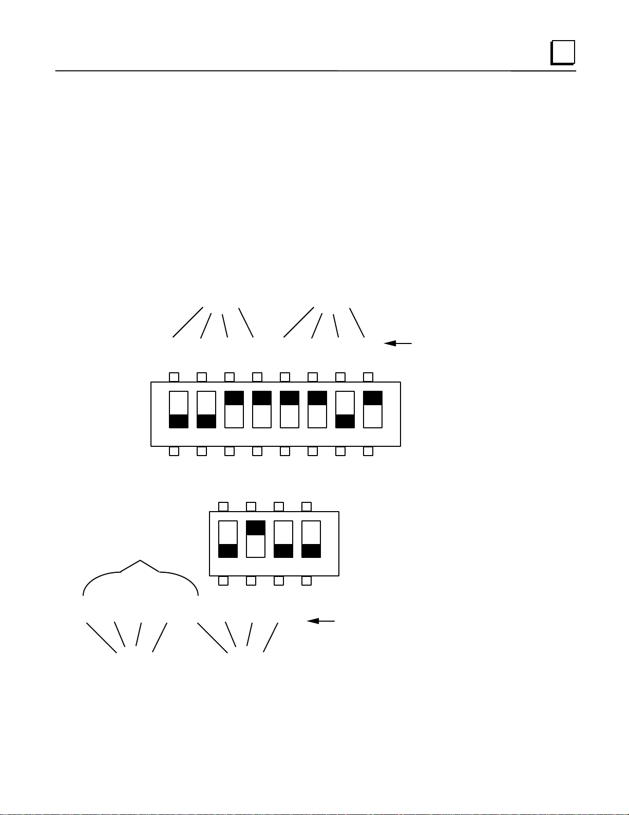
B
Board Address Selection Switches
There are two address select DIP switches on-board the Digital-to-Analog Converter Board. Each
individual switch corresponds to an address bit, or is not used. If the switch is ON the
corresponding address bit is compared to a logic "zero". All corresponding address bits must
compare with the switch positions during a Write/Read of the DAC board. Each switch corresponds
to the address bits as shown in Figure 2-1 be low. For the board switch locations are shown in
Figure 2-2 on page 2-6.
Example: For the Digital-to-Analog Converter Board to respond to a base address of
(FXFFBC40
) the S1 and S2 switches would be set accordingly.
16
Figure 2-1. Address Selection Switches
C
16
2
16
0011
A08 A09 A10 A11 A12 A13 A14 A15
*
0000
2
1101
2
A05 A06 A07
4321
0010
2
NOT
USED
X
READ THIS DIRECTION
2
OFF, OPEN = 1
S2
ON, CLOSED = 087654321
OFF
S1
ON
READ THIS DIRECTION
04
16
*No switches on-board to represent bits A00 through A04. These bits are understood to
be "zeros".
GFK-2059 Chapter 2 Configuration and Installation 2-5
16
Page 13
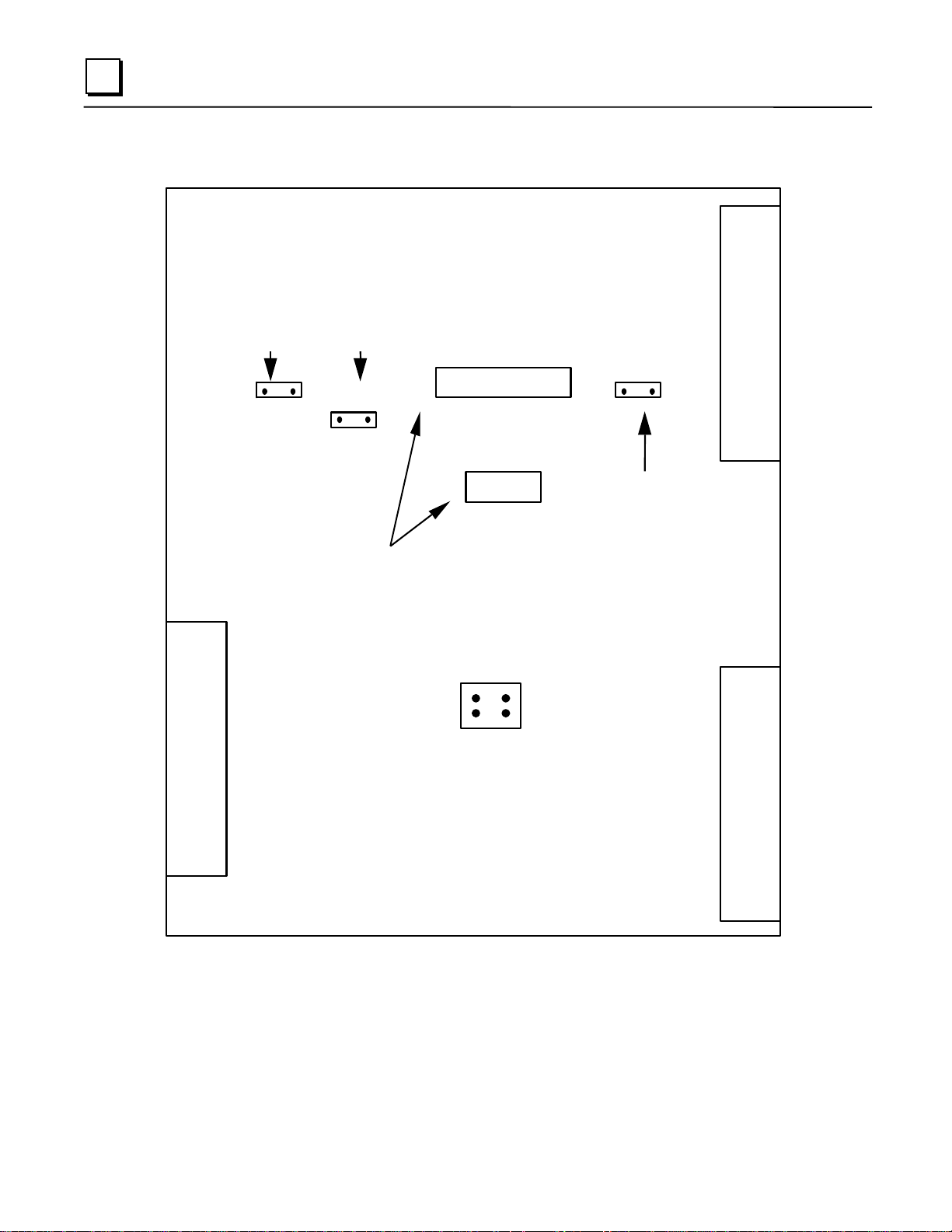
2
CODE SELECTION
Figure 2-2: Jumper and Switch Locations on the Digital-to-Analog
Converter Board
MODE JUMPER
DAC UPDATE
JD
EXTERNAL
JE
TRIGGER JUMPER
S2
P1
JC
S1
P3
SWITCHES
BOARD BASE
ADDRESS SELECTION
JA
JUMPER
DAC BINARY
JB
ADDRESS MODIFIER
JUMPER
P2
COMPONENT SIDE SHOWN
2-6 IC697VAL348 8-Channel, 16-bit Digital-to-Analog Converter Board User’s Manual GFK-2059
– December 2001
Page 14

Address Modifier Response Selection
The DAC board is memory mapped in the short I/O address space as described in Chapter 3. The
DAC board will respond to either of the two address modi fier codes that may be issued to the DAC
board by a CPU board during a Write or Read cycle. The DAC board is factory set to respond to
supervisory short I/O access. To select short nonprivileged I/O access, and install the jumper at
jumper location (JC).
2
GFK-2059 Chapter 2 Configuration and Installation 2-7
Page 15

2
Digital Code Selection
The DAC board is factory configured for offset binary coding. To change the DAC input coding to
two’s complement binary, remove jumper JA and install jumper JB (see Figure 2-3 below).
Figure 2-3: Digital Code Selection
JA
JB
(TWO’S COMPLEMENT CODE)(OFFSET BINARY)
2-8 IC697VAL348 8-Channel, 16-bit Digital-to-Analog Converter Board User’s Manual GFK-2059
– December 2001
Page 16

Program Controlled and External Start Convert Mode
The PROGRAM CONTROLLED START CONVERT MODE is enabled by inserting jumper JD.
This mode is detailed in “Program Control Update Mode” on page 4-4 and “Delayed DAC Update
Mode” on page 3-6. With no jumper installed at JD, the board operates in the IMMEDIATE DAC
UPDATE MODE as described in “Immediate DAC Update Mode” on page 4-3 and “Immediate
DAC Update Mode” on page 3-3.
Installing jumper JE enables the EXTERNAL START CONVERT MODE. Jumper JD must also
be installed (refer to “External Trigger Update Mode” on page 4-4). The external trigger is buffered
in through the P2 connector pin A25 with an associated digital ground wire at pin A26. The
locations of jumpers JD and JE are shown in Figure 2-2 on page 2-6.
2
GFK-2059 Chapter 2 Configuration and Installation 2-9
Page 17

2
Connector Descriptions
Two 96-pin DIN type connectors, P1 and P2, connect the DAC board to the VMEbus backplane.
The primary connector, P1, contains the address d a ta and control lines and all additional signals
necessary to control data transfer and other bus functions. See Figure 2-4 on page 2-11 and Table
2-2 on page 2-12 for the P2 connector signal assignments.
The P3 connector is a Panduit 32-pin male connector type, number 120-332-033A. The matching
Panduit connector for the input cable is a female connector type, number 120-332-435E. This
connector handles the 16 analog outputs, each with an associated analog ground wire. See Figure 25 on page 2-13 and Table 2-3 on page 2-14 for P3 connector assignment.
2-10 IC697VAL348 8-Channel, 16-bit Digital-to-Analog Converter Board User’s Manual GFK-2059
– December 2001
Page 18

PC BOARD
2
Figure 2-4: P2 Connector – Pin Assignments
ROW
C B A
PIN 1
PIN 2
PIN 3
PIN 4
PIN 5
PIN 6
PIN 7
PIN 8
PIN 9
PIN 10
PIN 11
PIN 12
PIN 13
PIN 14
PIN 15
PIN 16
PIN 17
PIN 18
PIN 19
PIN 20
PIN 21
PIN 22
PIN 23
PIN 24
PIN 25
PIN 26
PIN 27
PIN 28
PIN 29
PIN 30
PIN 31
PIN 32
REAR VIEW
GFK-2059 Chapter 2 Configuration and Installation 2-11
Page 19

2
Table 2-2: P2 Connector
Pin Number
1 ANA COM +5V
2 ANA COM GND
3 ANA COM
4 ANA COM
5 ANA COM
6 ANA COM
7 AINTESTBS
8 ANA COM
9
10 ANA COM
11
12 ANA COM GND
13 +5V
14 ANA COM
15 GND SEN
16 ANA COM
17
18 ANA COM
19
20 ANA COM
21
22 ANA COM GND
23 ANA COM
24 ANA COM
25 EXTSCL
26 GND
27
28
29
30
31 GND
32 +5V
Row A
Signal Mnemonic
Row B
Signal Mnemonic
Row C
Signal Mnemonic
2-12 IC697VAL348 8-Channel, 16-bit Digital-to-Analog Converter Board User’s Manual GFK-2059
– December 2001
Page 20

"PC Board"
2
Figure 2-5: P3 Connector – Pin Assignments
ROW
A C*
PIN 16
PIN 15
PIN 14
PIN 13
PIN 12
PIN 11
PIN 10
PIN 9
PIN 8
PIN 7
PIN 6
PIN 5
PIN 4
PIN 3
PIN 2
FRONT VIEW
OF "P3"
CONNECTOR
PIN 1
*Row C pins are all analog common
GFK-2059 Chapter 2 Configuration and Installation 2-13
Page 21

2
Table 2-3: P3 Connector
Pin Number
1 ANA COM ANA COM
2 AN00 ANA COM
3 AN01 ANA COM
4 AN02 ANA COM
5 AN03 ANA COM
6 AN04 ANA COM
7 AN05 ANA COM
8 AN06
9 AN07
10
11
12
13
14
15
16
Row A
Signal Mnemonic
Row B
Signal Mnemonic
Row C
Signal Mnemonic
2-14 IC697VAL348 8-Channel, 16-bit Digital-to-Analog Converter Board User’s Manual GFK-2059
– December 2001
Page 22

DAC Zero Offset and Gain Calibration
Note
This procedure assumes that the offset binary coding jumper (JA) is
selected.
1. Remove power from the Digital-to-Analog Converter Board.
2. Remove any cable connected to the P3 connector.
3. Remove the Digital-to-Analo g Converter Board from the chassis assembly and install a
VMEbus Extender board in its place.
4. Install the Digital-to-Analog Converter Board onto the VMEbus Extender board.
5. Apply power to the module and allow 15 minutes for Temperature Stabilization before
making any measurements.
6. Using the IMMEDIATE UPDATE MODE write digital code 4100 HEX to the CSR
location XXXX0070. This HEX code is the Control Word for output to the Digital-to-
Analog Converter Board’s P3 connector.
2
7. Write 8000 HEX to each of the eight DAC channels at addresses XXXX0060 through
XXXX006E.
8. Using a 6-digit multimeter, monitor each DAC output at the P3 connector. Connect the
negative lead to connector P3 pin C2. Adjust each DAC's offset potentiometer for a
voltage of 0.0000 ±60 µ V. Refer to Table 2-4 below and Figure 2-6 on page 2-16 for the
Potentiometer Location and P3 connector pin for each channel.
Table 2-4. Digital-to-Analog Converter Board Calibration Table
Channel Offest Pot Gain Pot P3 Connector
1 R23 R21 A2
2 R19 R17 A3
3 R31 R29 A4
4 R27 R25 A5
5 R3 R1 A6
6 R7 R5 A7
7 R15 R13 A8
8 R11 R9 A9
9. Repeat Step 7 using digital code FFFF HEX.
10. Using the multimeter, monitor each DAC output at t he P3 connector. Connect the negative
lead to connector P3 pin C2. Adjust each DAC's gain potentiometer for a voltage of
9.99969 ±60 µV. Refer to Table 2-4 above and Figure 2-6 on page 2-16 for the
Potentiometer Location and P3 connector pin for each channel.
11. Remove extender and re-install board into the chassis. Calibration completed.
GFK-2059 Chapter 2 Configuration and Installation 2-15
Page 23

2
Figure 2-6: Calibration Adjustment Locations
P1
16
R29
R17 R25
P3
R11 R19 R27
R1 R9
1
R3
R21
R13
R5
P2
R15 R23 R31
R7
COMPONENT SIDE
2-16 IC697VAL348 8-Channel, 16-bit Digital-to-Analog Converter Board User’s Manual GFK-2059
– December 2001
Page 24

Chapter
3
Programming
This chapter co ntains programming instructions for the Digital-to-Analog Converte r Board, and is
divided into the following sections:
Introduction to Programming the Digital-to-Analo g Converter Board
Digital-to-Analog Converter Board Progra mming Optio ns
Delayed DAC Update Mode
Test Mode Programming
Program Example (Delayed DAC Update Mode)
GFK-2059 3-1
Page 25

3
Introduction to Programming the Digital-to-Analog Converter Board
The Digital-to-Analog Converter Board is memory mapped in the short I/O address space. The
board occupies 16 successive word locations in the VME short I/O address space of 65,535 bytes.
Only the first nine word locations are actually used by the board. The short I/O space is located
from XXXX0000 HEX to XXXXFFFF HEX. The address bits A31 to A16 are CPU dependent.
Each Read cycle may be either a word or byte transfer. The board base address may be selected by
DIP switches as shown in “Board Address Selection Switches” on page 2-5. Tables 3-1 and 3-2
below represent the DAC address map assuming the factory set base address of XXXX0060 HEX.
Table 3-1:Control and Status Register
Control and Status Register (CSR) (Read/Write) Address $XXXX0070
D15 D14 D13 D12 D11 D10 D09 D08
Not
Used
Control and Status Register (CSR) (Read/Write) Address $XXXX0070
D07 D06 D05 D04 D03 D02 D01 D00
Control and Status Bits
Not Used
Table 3-2: DAC Channels Address Map
DAC Channels (0 to 7) Address (Write Only)
Address D15 (MSB) D00 (LSB)
XXXX0060 DAC OUT 0
XXXX0062 DAC OUT 1
XXXX0064 DAC OUT 2
XXXX0066 DAC OUT 3
XXXX0068 DAC OUT 4
XXXX006A DAC OUT 5
XXXX006C DAC OUT 6
XXXX006E DAC OUT 7
Note
Jumper JC determines whether the board operates in Short Supervisory I/O
Access or Short NonPrivileged I/O Access. With the jumper installed Short
NonPrivileged I/O Access is selected.
Tables 3-1 and 3-2 above shows addressing information for 16-bit word transfers. Data may be
transferred to the DACs in 8-bit format. When using byte format, the low byte is always transferred
first then the high byte next. For example, assuming a board base address of XXXX0000 HEX, a
low byte transfer (D7 to D0) to Channel 0 is written to address XXXX0001 HEX. The high byte of
data (D15 to D8) is then written to address XXXX0000 HEX.
3-2 IC697VAL348 8-Channel, 16-bit Digital-to-Analog Converter Board User’s Manual GFK-2059
– December 2001
Page 26

Digital-to-Analog Converter Board Programming Options
There are two types of registers that must be written to for prop er operation of the DAC board. One
is the CSR, and the other is the DAC. The order in which they are written to may differ depending
on the method used to start a conversion.
Immediate DAC Update Mode
The IMMEDIATE DAC UPDATE MODE is described in “Program Control Update Mode” on
page 4-4 and the board is configured for this mode when received from the factory. Once this has
been set up, a 16-bit word can be written to any DAC channel where it will begin immediate analog
conversion. When byte transfer (8-bit) is used to load the DAC channel, conversion begi ns
immediately upon the loading of the high byte (D15 to D8).
All eight DAC channels can be initiated to a value, as described in the preceding paragraph, before
they are connected to the external circuitry. After powering up the board, load the DAC channels
with the initial 16-bit word (or two 8-bit bytes) required (positive true offset binary or binary two's
complement coding, Table 3-3 below). A control word can then be written to the CSR to enable the
DAC outputs to the P3 connecto r . The CSR bit description for this mode of operation is detailed in
Table 3-4 on page 3-4 and Table 3-5 on page 3-5.
3
Table 3-3. DAC Data Format Analog Output versu s Digital Input (±10 V Scale)
Offset Binary Coding
Digital Input Code
(MSB)
D15
0000 0000 0000 0000 -10.000V -Full Scale 1000 0000 0000 0000
0100 0000 0000 0000 -5.000V -1/2 Scale 1100 0000 0000 0000
1000 0000 0000 0000 0.000V Zero 0000 0000 0000 0000
1000 0000 0000 0001
1100 0000 0000 0000 +5.000V +1/2 Scale 0100 0000 0000 0000
1111 1111 1111 1111 9.99969V +Full Scale 0111 1111 1111 1111
The analog output may be calculated by the input code written by the processor to the selected
DAC channel as follows:
(LSB)
D0
Analog Output = -10 V +
Analog Output Voltage Two’s Complement
305µV
+LSB 0000 0000 0000 0001
([(Digital Input Code in decimal) X 20] /65536)
GFK-2059 Chapter 3 Programming 3-3
Page 27

3
Example: The analog output for a digital input of 0A00H would be:
1. 0A00H decimal equivalent is 2560
2. Analog out = -10 V +
((2560) __20__)
65,536
= -9.21875
Table 3-4. Control Register Data Format and Definitions
Control and Status Register
D15 D14 D13 D12 D11 D10 D09 D08
Not
Used
Control and Status Register
D07 D06 D05 D04 D03 D02 D01 D00
Not Used
Bit D15: Not used.
Bit D14: A low state turns the Fail LED ON. A high state turns the Fail LED OFF.
At power-up this control bit is low.
Bit D13: A high state enables the selected analog output to pass out the P2 connector
on test bus 2 (AOTESTBS). At power-up this control bit is low.
Bit D12: A high state enables the selected analog output to pass out the P2 connector
on test bus 1 (AINTESTBS). At power-up this control bit is low.
Bit D11
(1)
: When written high, it engages one analog output from the DAC to one of
two test buses. Used in conjunction with D12 and D13 to determine which
test bus is selected. At power-up this control b it is low which disengages
the test buses.
Not
Used
Bit D10: Not used.
Bit D09: Program Control Start Convert. When set to a "one", it generates a signal
that transfers contents of previously loaded DACs to the second rank
register and updates the analog output.
Bit D08: Don’t care
Bits 07 through 00: Not used.
(1) Channel selection for muxing one of the outputs to either test bus is achieved by writing the
CSR data to the data address + 10H. See “T est Mode Programming” on page 3-7 for additional
information.
3-4 IC697VAL348 8-Channel, 16-bit Digital-to-Analog Converter Board User’s Manual GFK-2059
– December 2001
Page 28

3
Table 3-5: Programming the Control and Status Register for Different Analog Output Variations – Bit
Definitions
Analog Output Over TEST BUS 1 (AINTESTBS)
D15 D14 D13 D12 D11 D10 D09 D08
Not
Used
1 0 1 1
Analog Output Over TEST BUS 2 (AINTESTBS)
D15 D14 D13 D12 D11 D10 D09 D08
Not
Used
1 1 0 1
Analog Output Over TEST BUS 1 and Over P3 Connector to Field-co nnected
Device (Used for Real-time Fault Detection of DACs)
D15 D14 D13 D12 D11 D10 D09 D08
Not
Used
1 1 0 1
Analog Output Over P3 Connector Only
D15 D14 D13 D12 D11 D10 D09 D08
Not
Used
1 0 0 0
Not
Used
Not
Used
Not
Used
Not
Used
0 or 1 0
0 or 1 0
0 or 1 1
0 or 1 1
GFK-2059 Chapter 3 Programming 3-5
Page 29

3
Delayed DAC Update Mode
The DELAYED DAC UPDATE MODE operation is described in “Delayed DAC Update Mode”
on page 4-4. This mode must have previously been enabled by the jumper configuration in
“Program Controlled and External Start Convert Mode” on page 2-9. There are two ways for a
DAC channel to be updated after the 16-bit word is loaded into the DAC's first register. The first
way is under program control when data bit D9 is written high to the CS R. It should be noted that
when setting D9 to initiate t he DAC update that control bits D8, and D11 through D14 should be
set or reset according to where the user wants the converted output to be routed, (refer to Table 3-4
on page 3-4 and Table 3-5 on page 3-5). Also, a previously loaded DAC may be updated by an
external trigger input from another device. A programming example of the DELAYED DAC
UPDATE MODE is detailed in “Program Example (Delayed DAC Update Mode)” on page 3-9.
3-6 IC697VAL348 8-Channel, 16-bit Digital-to-Analog Converter Board User’s Manual GFK-2059
– December 2001
Page 30

Test Mode Programming
Any of the eight DAC outputs may be selected to pass to an ADC board over test bus 2 to verify
the DAC outputs. If a MUX is present in the analog backplane then any DAC output can be
selected to go to that board for test purposes over test bus 1. Generally the programming sequence
for utilizing one of the two test buses is as follows:
If IMMEDIATE DAC UPDATE MODE is employed, then a Control Word should first be written
to the CSR. This Control Wo rd information includes which test bus the DAC output is to be routed
to, and whether the output is to be isolated or connected to the P3 connector (refer to Table 3-4 on
page 3-4 and Table 3-5 on page 3-5). The DAC to be updated is then loaded with a 16-bit word.
The channel is updated and passes out the selected test bus.
An output may also be updated under program control to route to a specified test bus. The board
must have previously been jumpered to accommodate the DELAYED DAC UPDATE MODE as
shown in “Program Controlled and External Start Convert Mode” on page 2-9. The programming
sequence is as follows:
First, a 16-bit word or two 8-bit bytes are written to the add ress of the DAC channel that is to b e
updated. The data is stored in the DAC Register and will be converted by setting the proper bits in
a Write cycle to the CSR. The CSR must be written to at the same address as that of the DAC
channel that has previously been loaded plus 10 HEX. For example, if the user wanted to convert
Channel no. 2 which was written to address XXXX0062 HEX, then the Control Word would be
written to address XXXX0072 HEX (XXXX0062 and 10 HEX). Data bit D09 when written as
"one" to the CSR initiates the analo g conversion of the previously stored 16-bit word.
3
The test modes can only be used if an ADC board exists in the same GE Fanuc analog (P2)
backplane as the Digital-to-Analog Converter Board.
GFK-2059 Chapter 3 Programming 3-7
Page 31

3
Program Example (Delayed DAC Update Mode)
In the programming example in “Test Mode Programming” on page 3-7, all eight DAC converters
were loaded with a full scale value of FFFH in the IMMEDIATE UPDATE MODE. For illustration
purposes the same result will be obtained by this programming example by using the DELAYED
DAC UPDATE MODE. The DELAYED DAC MODE is jumper-selectable as described in
“Program Controlled and External Start Convert Mode” on page 2-9.
The programming sequence in a flowchart is shown in Figure 3-2 on page 3-12. In the following
program example all eight DAC channels are loaded with new data, and then updated under
program control. Alternatively, if previously enabled, an external trigger input could have initiated
the DAC conversion process.
3-8 IC697VAL348 8-Channel, 16-bit Digital-to-Analog Converter Board User’s Manual GFK-2059
– December 2001
Page 32

CONTROL
REGISTER
ALL 8 D/A
CHANNEL
END
3
Figure 3-1: DAC Programming Sequence (Immediate DADC Start Convert Mode)
-
INITIALIZATION)
-
LOAD D/A
INITIALIZE
D/A ADDRESS
POINTER
LOAD
HAVE
GFK-2059 Chapter 3 Programming 3-9
BEEN
?
YES
NO
Page 33

3
Table 3-6: Analog Output Control in Immediate DAC Update Mode
Analog Out Pathway Control Word (D15 to D0) Hex Value
P3 Connector 4100
AOTESTBS (TEST BUS 2) 6C00
AINTESTBS (TEST BUS 1) 5C00
AOTESTBS and P3 Connector 6D00
3-10 IC697VAL348 8-Channel, 16-bit Digital-to-Analog Converter Board User’s Manual GFK-2059
– December 2001
Page 34

(ON-BOARD
INITIALIZE
POINTER
CHANNEL
UPDATED
END
CONTROL
REGISTER
3
Figure 3-2: DAC Programming Sequence (Delayed DAC Update Mode)
POWER-UP
LOAD
BEEN
LOAD D/A
YES
NO
GFK-2059 Chapter 3 Programming 3-11
Page 35

3
Table 3-7: Analog Output Control in Delayed DAC Update Mode
Analog Out Pathway Control Word (D15 to D0) Hex Value
P3 Connector 4300
AOTESTBS (TEST BUS 2) 6E00
AINTESTBS (TEST BUS 1) 5E00
AOTESTBS and P3 Connector 6F00
3-12 IC697VAL348 8-Channel, 16-bit Digital-to-Analog Converter Board User’s Manual GFK-2059
– December 2001
Page 36

Chapter
4
Theory of Operation
This chapter discusses the operatio n of the Digital-to-Analog Converter Board, and is divided into
the following sections:
Operational Overview
Immediate DAC Update Mode
Delayed DAC Update Mode
VMEbus Interface Description
GFK-2059 4-1
Page 37

4
Operational Overview
The Digital-to-Analog Converter B oard performs digital-to-analog conversion on 16-bit positive
true offset binary or two’s complement coded words, with an analog output range of -10 to +10 V.
This provides for a resolution of 305 µV for each digital input of 1 LSB change. The buffered
output voltage settles to wit hin 1/2 LSB in 10 µs.
The DAC offers a Digital-to-Analog I ntegrated Circuit (IC) per channel. A Control and St atus
Register (CSR) is loaded by the processor and this register controls the functioning of the board.
The processor can read the CSR at any time. The DAC board functional block diagram is shown in
Figure 4-1 on page 4-5. Double-buffered data latches precede each of the eight DACs. The data
latches allow versatility in the way that the DAC analog output may be upd a ted.
There are three methods by which new data can be converted by a DAC.
Each method is enabled/disabled by on-board jumpers and is further controlled by a CSR that must
be loaded by the user (the CSR contents are described in Tables 3-1 and 3-2 on page 3-2, Table 3-4
on page 3-4, and Table 3-5 on page 3-5).
4-2 IC697VAL348 8-Channel, 16-bit Digital-to-Analog Converter Board User’s Manual GFK-2059
– December 2001
Page 38

Immediate DAC Update Mode
The processor unit sends the 16-bit word to be converted to the first register of the selected DAC. If
that DAC channel has previously been jumpered to, it will automatically pa ss the contents of the
first DAC register into the second register and update the analog output. There is one jumper that
enables/disables all eight DAC channe ls to be in the IMMEDIATE UPDATE MODE as described
above, or in the DELAYED UPDATE MODE. Jumper definition and locations are describ ed in
“Program Controlled and External Start Convert Mode” on page 2-9.
4
GFK-2059 Chapter 4 Theory of Operation 4-3
Page 39

4
Delayed DAC Update Mode
In the DELAYED DAC UPDATE MODE, the processor sends the 16-bit word to be converted to
the first DAC register of the selected DAC. The data is stored there and transferred to the second
DAC register in one of two possible methods, described below.
Program Control Update Mode
One way for the transfer to occur is by writing a "one" to the Control Register bit D09. When the
data is transferred to the second register, digital-to-analog conversion begins and the analog output
settles to within 1/2 LSB in 10 µs. This method of updating the analog output is useful when more
than one DAC channel output is desired to change at a precise time. All eight DAC outputs could
be synchronized to change at certain periodic intervals under software control.
External Trigger Update Mode
The second method to update the second storage register and the DAC output by an external TTL
compatible trigger. This trigger must first have t he external trigger circuitry enabled by installing
an on-board jumper as described in “Program Controlled and External Start Convert Mode” on
page 2-9. The PROGRAM CONTROL UPDATE MODE must also be enabled (refer to “Program
Controlled and External Start Convert Mode” on page 2-9). When the external trigger is received
(active low for a minimum of 150 ns), the value stored in the first DAC register will be transferred
to the second DAC register and begins a conversion. Using this method of updating, all
conversions can be synchronized to an external d evice.
Each of the DAC outputs may be multiplexed one at a time via the test MUX shown in Figure 4-3
on page 4-8. First, a control word must be written to t he CS R to establish whether the analog output
is to be connected or disconnected from the P3 connector and which one of two test buses the
output is to be routed to. The DAC channel to b e tested has test data written to it in the
IMMEDIATE UPDATE MODE. Address bits A01 through A04 are automatically latched into the
Address Register when the board is written to. The outputs of this Add ress Register select the DAC
channel that has just been upd a ted via the test MUX. Test control infor mation previously latched in
the CSRs passes the DAC output through the analog test switch to the test bus 2. Test bus 2 is
routed via the analog backplane (AMXbus™) to the input of the ADC board where it is available
for analog-to-digital conversion. When the ADC completes its conversion, it se nds an end-ofconvert signal down the P2 backplane to the DAC. This signal removes either of the two test bus
outputs from the analog backplane. Along with the test bus 2 signal being sent to the ADC board
the analog ground (GND SEN) is switched out to the ADC board. This provides an input to the
ADC board, which is similar to a differential si gnal and is called pseudo-differential. Pseudodifferential solves some of the associated common mode error problems with single-ended signals.
The input to the ADC board is referenced to the grou nd of the DAC board instead of the local
ground at the ADC board, effectively canceling out common mode errors associated with different
ground potentials at each of the boards.
4-4 IC697VAL348 8-Channel, 16-bit Digital-to-Analog Converter Board User’s Manual GFK-2059
– December 2001
Page 40

CH 1
CH 2
CH 3
CH 4
DR SELECT
(
)
(
)
4
Figure 4-1: Digital-to-Analog Converter Board Functional Block Diagram
V
C
L
M
E
b
u
s
O
O
M
G
P
I
A
C
T
I
B
I
L
I
T
Y
PROGRAM
CONTROL UPDATE
16-BIT
DAC
NO. 1
DAC
SEL
16-BIT
DAC
NO. 2
DAC
SEL
16-BIT
DAC
NO. 3
DAC
SEL
16-BIT
DAC
NO. 4
DAC
SEL
DATA BUS
ADDRESS
REGISTER
OPERATION
AND CONTROL
LOGIC
8
CH 1
CH 8
EXTERNAL
UPDATE
16-BIT
DAC
NO. 5
16-BIT
DAC
NO. 6
16-BIT
DAC
NO. 7
16-BIT
DAC
NO. 8
DAC
SEL
ANALOG
OUT
ISOLATION
SWITCHES
DAC
SEL
DAC
SEL
DAC
SEL
CH 5
CH 6
CH 7
CH 8
P3
CH 1
CH 8
CSR
AOUT AD
SELECT AIN
TEST
SELECT A0
TEST
CH 8 CH 1
4
TEST
MODE
SAIT
SA0T
8-CHANNEL
MUX
DUAL
SPDT
SWITCH
A0 TEST
P2
A0IN TEST
A0 TEST
GFK-2059 Chapter 4 Theory of Operation 4-5
Page 41

4
VMEbus Interface Description
The VMEbus interface (Figure 4-4 on page 4-9) contains the necessary logic to interface a DAC
board to the VMEbus. The DAC is memory mapped in the VMEbus short I/O address space.
During a Write cycle to the board, address bits A05 through A15 are compared with the previously
selected board address. DIP switches select the board address. If the address compares, then a
board select signal is issued. This signal along with the control signals received at the board, gate
the data (D0 to D15) to a selected DAC or the CSR on the DAC. Address bits A01 through A03
select one of the eight DAC channels. Data D0 through D15 is latched into the selected DAC
Register. Address bit A04 is used to select the CSR.
The DAC circuitry requires +5 V, +15 V, and -15 V, the +5 V is supplied to the board via the P1
and P2 connectors. An on-board DC-to-DC converter generates the +15 V and -15 V for the analog
circuitry (refer to Figure 4-5 on page 4-11). Thus, the DAC board only needs +5 V from the chassis
power supply.
4-6 IC697VAL348 8-Channel, 16-bit Digital-to-Analog Converter Board User’s Manual GFK-2059
– December 2001
Page 42

GFK-2059 Chapter 4 Theory of Operation 4-7
REGISTER
A01
A02
A03
A04
ADDRESS
REGISTER
D/A CHANNEL SELECT
3
1
TEST
CLOCK
TEST BUS 1
DA
OUTPUTS
1 TO 8
TEST
MUX
MUX
OUT
1
ANALOG
TEST
SWITCH
TEST
CONTROL
3
TEST BUS 2
GND SEN
P2
Figure 4-2: Test Bus Logic
4
Page 43

4
VMEbus
CONNECTION (P1)
Figure 4-3: VMEbus Interface Logic and Interface Signals
21
A15 to A05
AM5 to AM0
A4 to A01
16
D15 to D0
1
DTACK
5
ADDRESS AND
ADDRESS
MODIFIER
COMPARATOR
TRANSCEIVER
TRANSCEIVER
BOARD
DATA
DATA
BOARD SELECT
1
D/A ADDRESS
D/A CONTROL
TO D/As
16
4
D/A
CHANNEL
4
ADDRESS
AND
CONTROL
REGISTER
INTERNAL DATA BUS
3
7
DTACK
GENERATOR
3
8
P2 CONNECTION
EXTERNAL
DA TRIGGER
4-8 IC697VAL348 8-Channel, 16-bit Digital-to-Analog Converter Board User’s Manual GFK-2059
– December 2001
TEST BUS NO. 1
TEST BUS NO. 2
GND SEN
1
EXTERNAL D/A TRIGGER
TO D/As
Page 44

P1
+15 V
4
Figure 4-4: Digital-to-Analog Converter Board Power
DIG GND
P2
+5 V
GND
GND
+5 V
DC-TO-DC
CONVERTER
+5 V
ANA
CO
GND
-15 V
DC-TO-DC
CONVERTER
+5 V
GND
ANA
CO
+5 V
-15 V
ANA COM
+15 V
GFK-2059 Chapter 4 Theory of Operation 4-9
Page 45

Chapter
5
Maintenance
This chapter provides information relative to the care and maintenance of the Digital-to-Analog
Converter Board.
If the product malfunctions, verify the following:
• Software
• System configuration
• Electrical connections
• Jumper or configuration optio ns
• Boards fully inserted into their proper connector location
• Connector pins are clean and free from contamination
• No components of adjacent boards are disturbed when inserting or removing the board
from the VMEbus card cage
• Quality of cables and I/O connections
User level repairs are not recommended. Contact GE Fanuc for a Return Material Authorization
(RMA) Number. This RMA Number must be obtained prior to any return.
GFK-2059 5-1
 Loading...