

Page 1
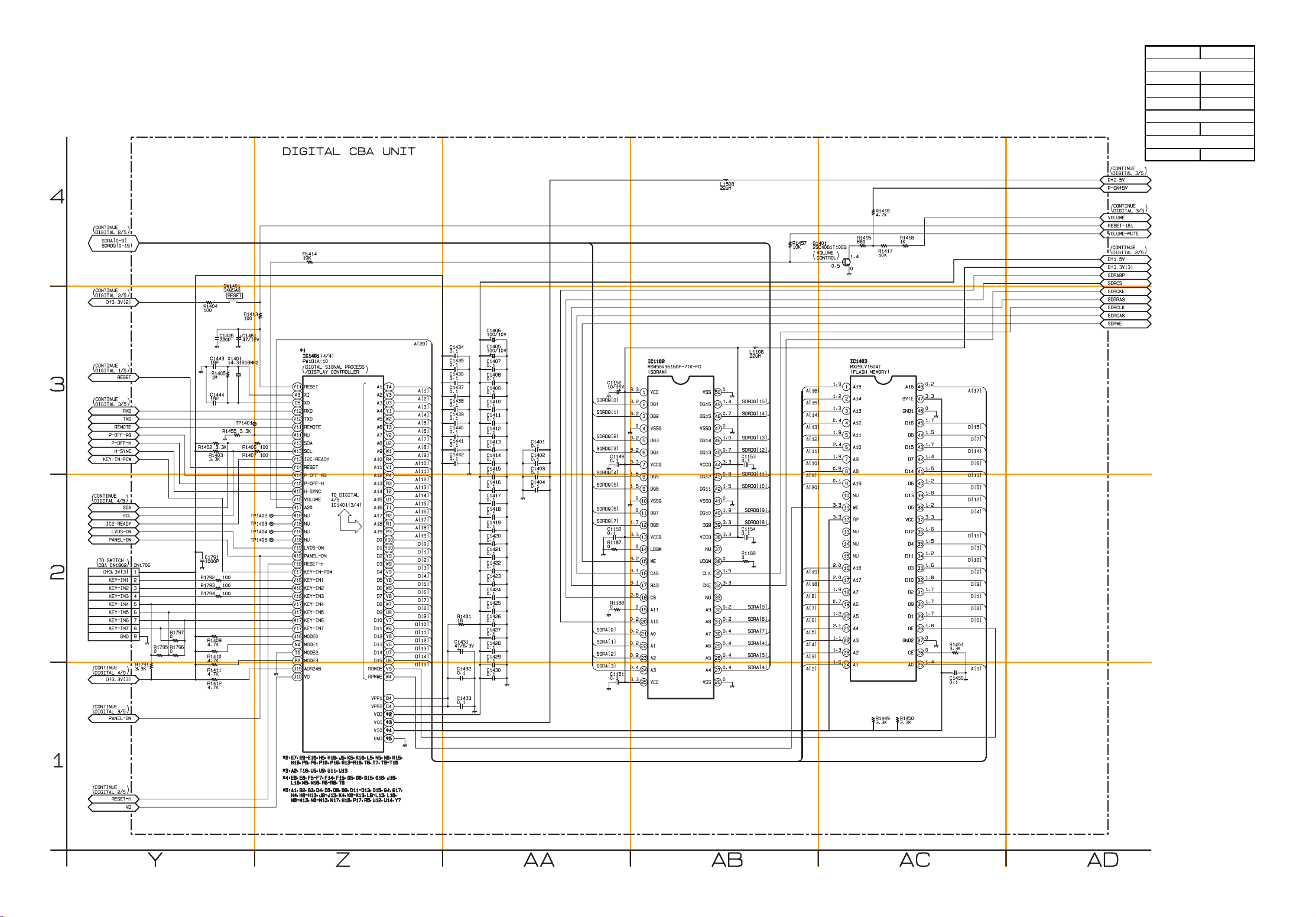
Digital 1/5 Schematic Diagram
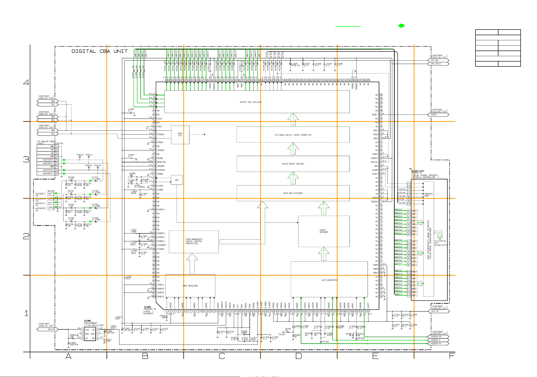
DIGITAL 1/5
Ref No. Position
IC1301
B-1
IC1401(1/4)
F-3
IC1501
A-1
CN1702 A-4
ICS
CONNECTOR
*1 Note:
1. The order of pins shown are different from that of IC1401 itself.
2. Some pins are not shown because they are not used.
3. IC1401 is shown as IC1401(1/4) through IC1401(4/4) in Digital Schematic Diagram section.
Video Signal
Audio Signal
A4
A3
B4
B3
C4
C3
D4
D3
E4
E3
F4
F3
A2
A1
B2
B1
1-9-3 1-9-4
C2
C1
D2
D1
E2
E1
F2
F1
L0605SCD1
Page 2
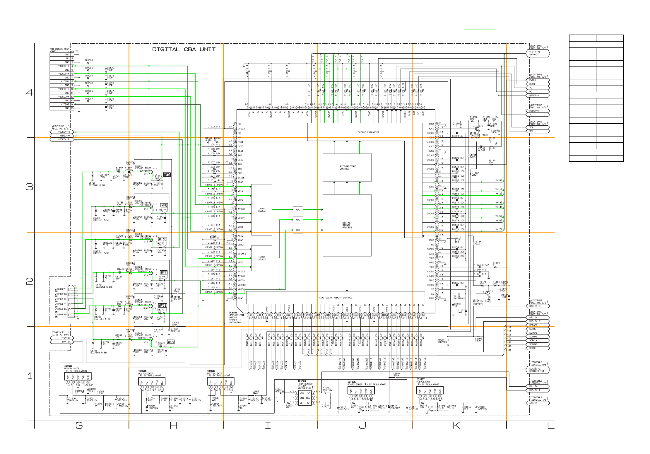
Digital 2/5 Schematic Diagram
DIGITAL 2/5
Ref No. Position
IC1101
I-2
IC1502
G-1
IC1503
I-1
IC1504
H-1
IC1505
H-1
IC1506
J-1
IC1507
K-1
Q1101
K-4
Q1102
K-2
Q1701
H-3
Q1702
H-3
Q1703
H-2
Q1704
H-2
Q1705
H-2
Q1706
H-1
CN1701 G-4
ICS
TRANSISTORS
CONNECTOR
Video Signal
G4
G3
H4
H3
I4
I3
J4
J3
K4
K3
L4
L3
G2
G1
H2
H1
1-9-5 1-9-6
I2
I1
J2
J1
K2
K1
L2
L1
L0605SCD2
Page 3
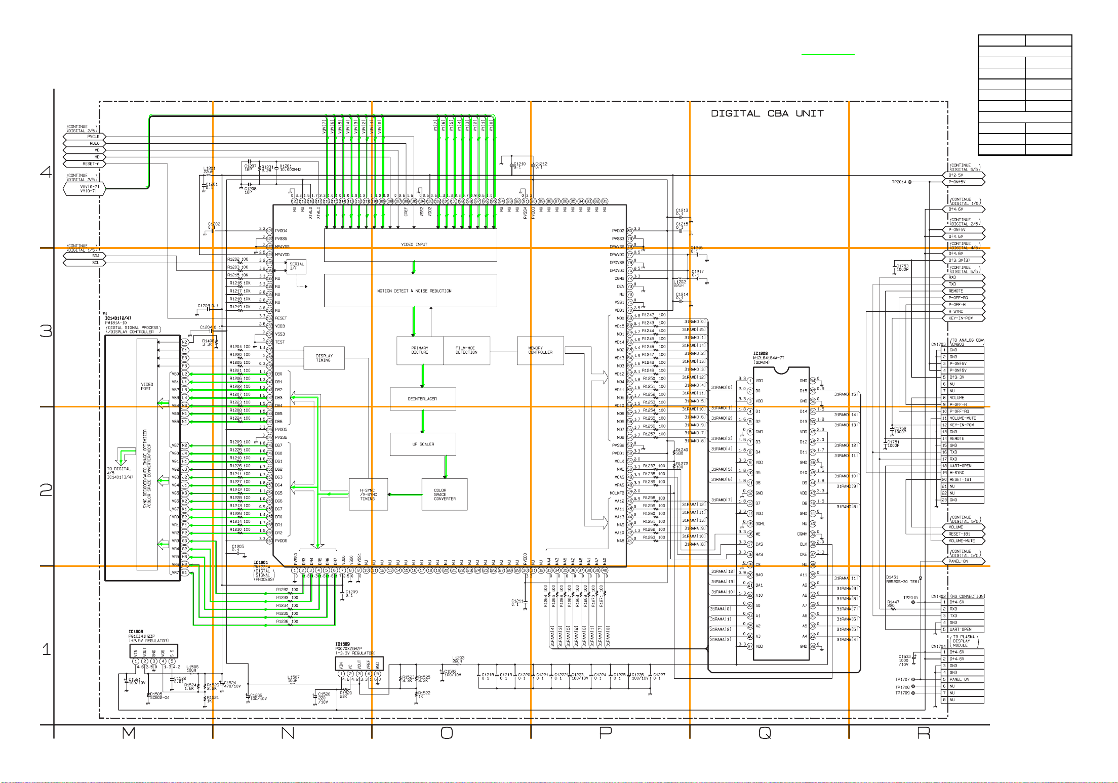
Digital 3/5 Schematic Diagram
DIGITAL 3/5
Ref No. Position
IC1201
N-2
IC1202
Q-3
IC1401(2/4)
M-3
IC1508
M-1
IC1509
N-1
CN1402
R-1
CN1703
R-3
CN1704 R-1
ICS
CONNECTORS
*1 Note:
1. The order of pins shown are different from that of IC1401 itself.
2. Some pins are not shown because they are not used.
3. IC1401 is shown as IC1401(1/4) through IC1401(4/4) in Digital Schematic Diagram section.
Video Signal
M4
M3
N4
N3
O4
O3
P4 Q4 R4
P3
Q3
R3
M2
M1
N2
N1
1-9-7 1-9-8
O2
O1
P2
P1
Q2
Q1
R2
R1
L0605SCD3
Page 4
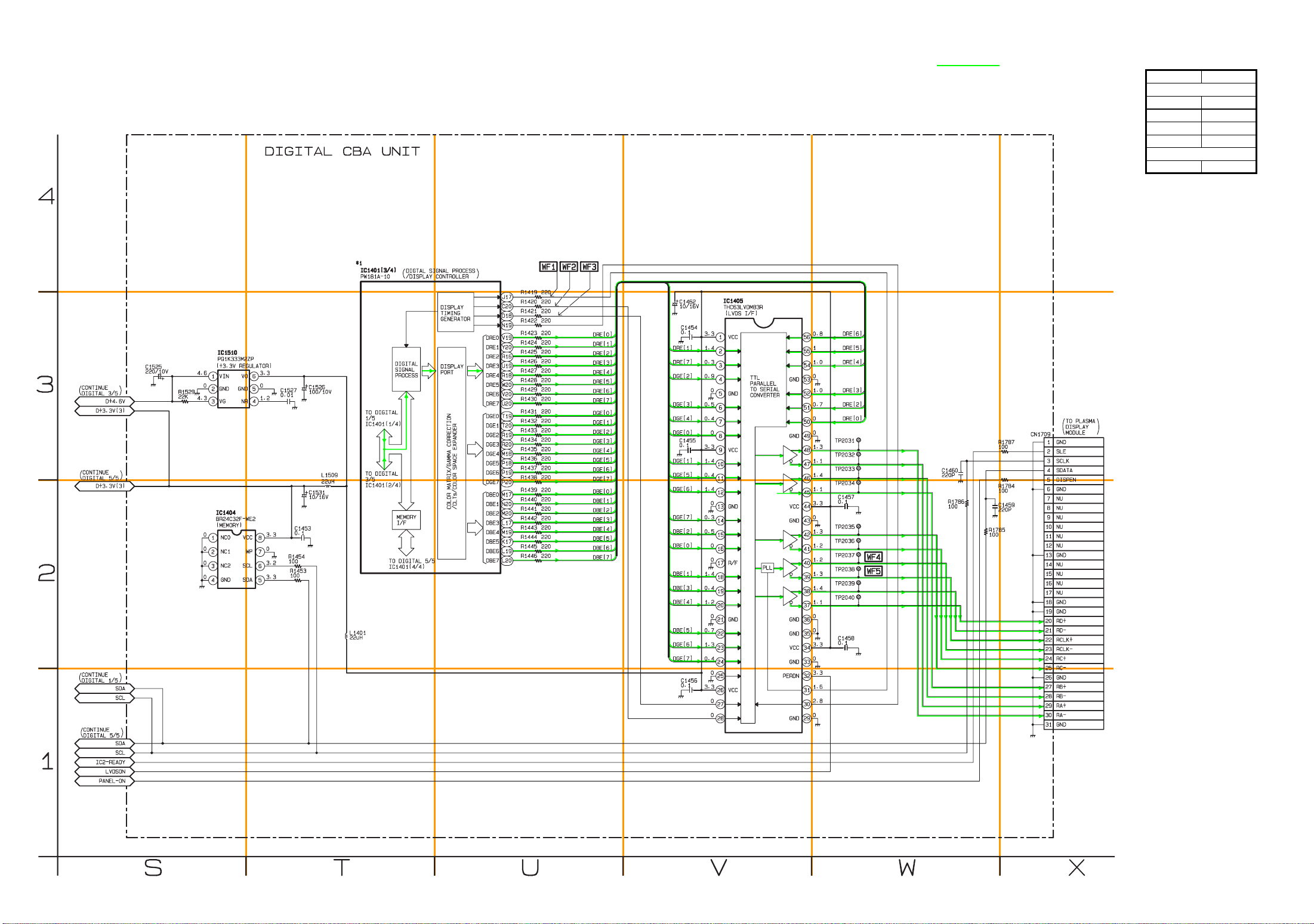
Digital 4/5 Schematic Diagram
DIGITAL 4/5
Ref No. Position
IC1401(3/4)
T-4
IC1404
S-2
IC1405
V-3
IC1510
S-3
CN1709 X-3
ICS
CONNECTOR
*1 Note:
1. The order of pins shown are different from that of IC1401 itself.
2. Some pins are not shown because they are not used.
3. IC1401 is shown as IC1401(1/4) through IC1401(4/4) in Digital Schematic Diagram section.
Video Signal
S4
S3
T4
T3
U4
U3
V4
V3
W4
W3
X4
X3
S2
S1
1-9-9
T2
T1
U2
U1
V2
V1
W2
W1
1-9-10
X2
X1
L0605SCD4
Page 5
Digital 5/5 Schematic Diagram
DIGITAL 5/5
Ref No. Position
IC1102
AB-3
IC1401(4/4)
Z-3
IC1403
AC-3
Q1401
AC-4
CN1706 Y-2
ICS
TRANSISTOR
CONNECTOR
*1 Note:
1. The order of pins shown are different from that of IC1401 itself.
2. Some pins are not shown because they are not used.
3. IC1401 is shown as IC1401(1/4) through IC1401(4/4) in Digital Schematic Diagram section.
Y4
Y3
Z4
Z3
AA4
AA3
AB4
AB3
AC4
AC3
AD4
AD3
Y2
Y1
Z2
Z1
1-9-11 1-9-12
AA2
AA1
AB2
AB1
AC2
AC1
AD2
AD1
L0605SCD5
Page 6
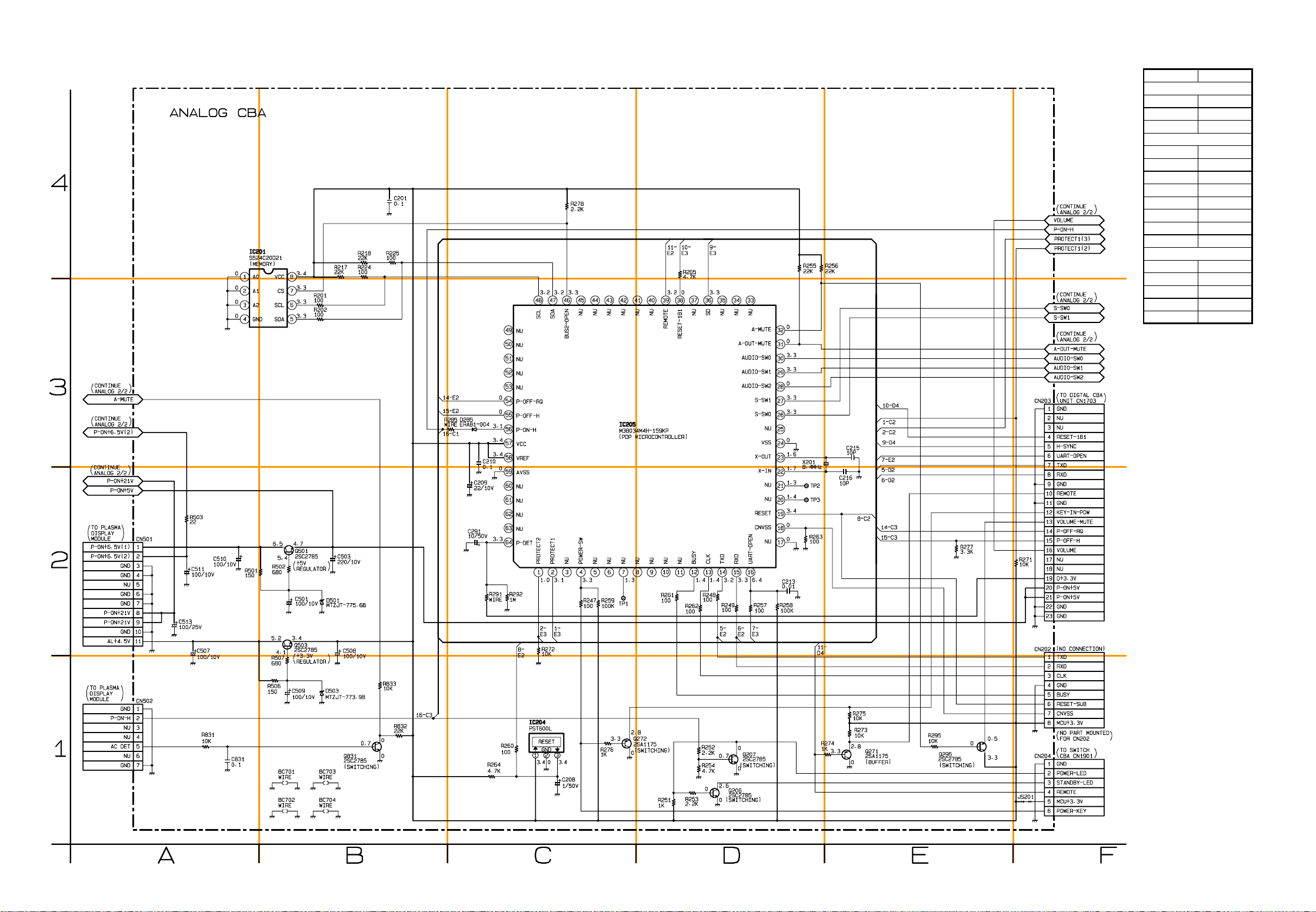
Analog 1/2 Schematic Diagram
ANALOG 1/ 2
Ref No. Position
IC201
B-4
IC204
C-1
IC205
D-3
Q206
D-1
Q207
D-1
Q271
E-1
Q272
C-1
Q295
E-1
Q501
B-2
Q503
B-2
Q831
B-1
CN202
F-2
CN203
F-3
CN204
F-1
CN501
A-2
CN502 A-1
ICS
TRANSISTORS
CONNECTORS
A4
A3
B4
B3
C4
C3
D4
D3
E4
E3
F4
F3
A2
A1
1-9-13
B2
B1
C2
C1
D2
D1
E2
E1
1-9-14
F2
F1
L0605SCA1
Page 7
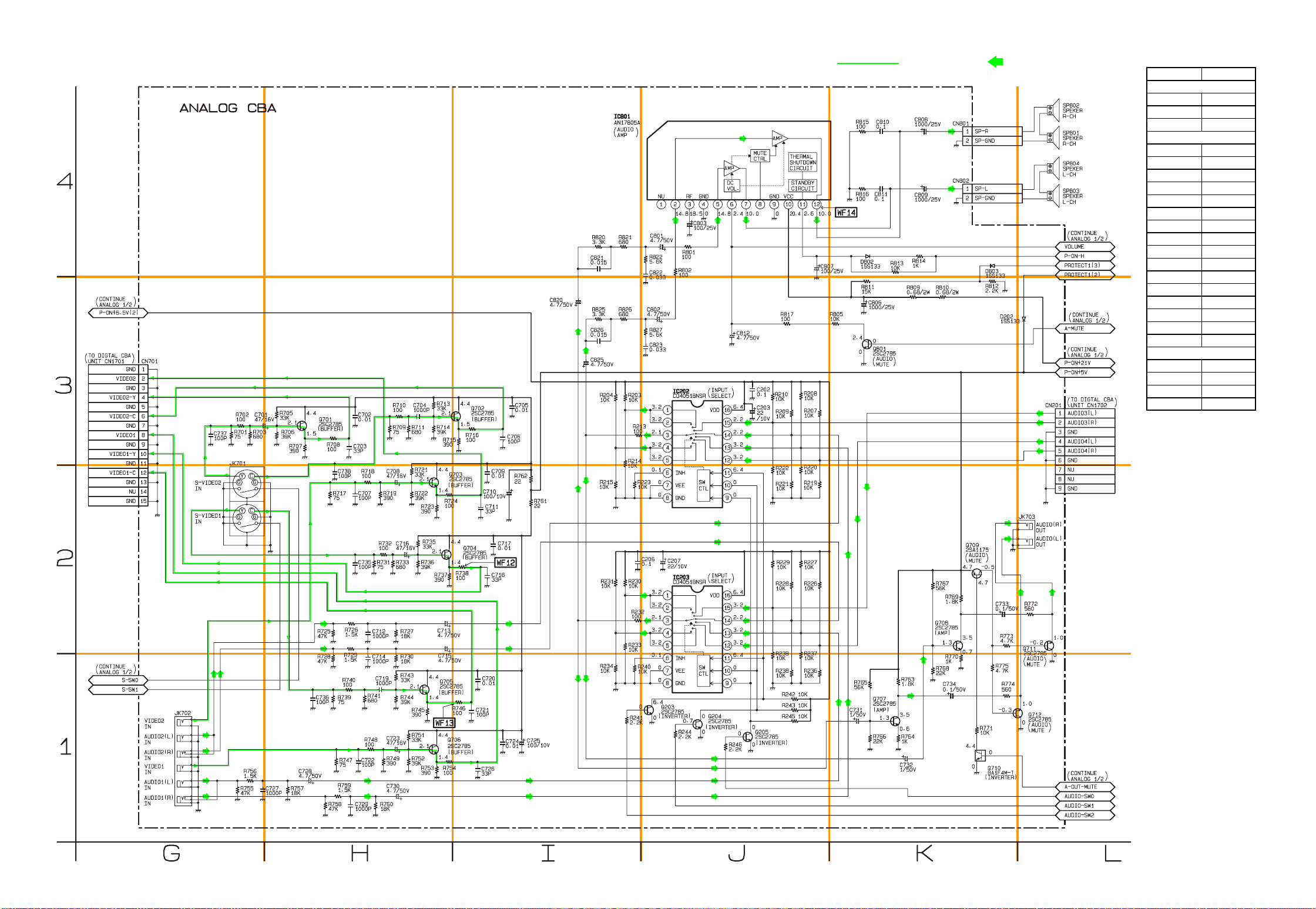
Analog 2/2 Schematic Diagram
ANALOG 2/ 2
Ref No. Position
IC202
J-3
IC203
J-2
IC801
J-4
Q203
J-1
Q204
J-1
Q205
J-1
Q701
H-3
Q702
I-3
Q703
H-2
Q704
H-2
Q705
H-1
Q706
H-1
Q707
K-1
Q708
K-2
Q709
K-2
Q710
K-1
Q711
L-2
Q712
L-1
Q801
K-3
CN201
L-3
CN701
G-3
CN801
K-4
CN802 K-4
ICS
TRANSISTORS
CONNECTORS
G4
G3
H4
H3
I4
I3
Video Signal
Audio Signal
J4 K4 L4
J3
K3
L3
G2
G1
H2
H1
I2
I1
J2
J1
K2
K1
L2
L1
1-9-15 1-9-16
L0605SCA2
Page 8
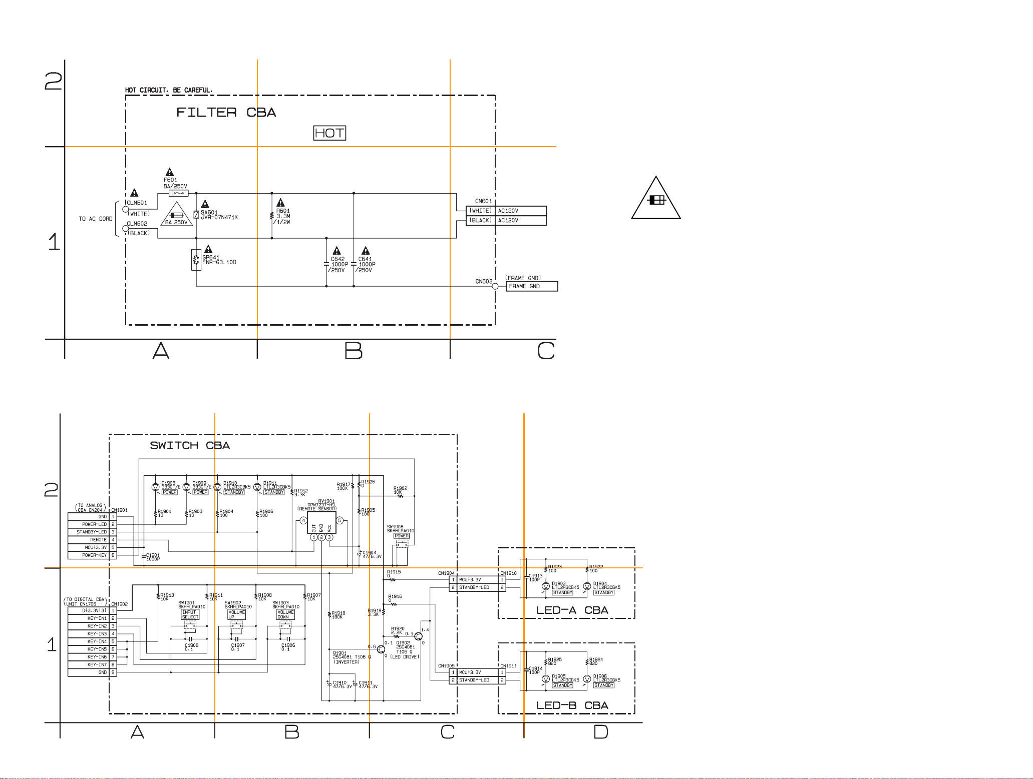
Filter Schematic Diagram
Filter Schematic Diagram
A2
A1
B2
B1
C2
C1
L0605SCF
CAUTION !
Fixed voltage ( or Auto voltage selectable ) power supply circuit is used in this unit.
If Main Fuse (F601) is blown, check to see that all components in the power supply
circuit are not defective before you connect the AC plug to the AC power supply.
Otherwise it may cause some components in the power supply circuit to fail.
CAUTION: FOR CONTINUED PROTECTION AGAINST RISK
OF FIRE, REPLACE ONLY WITH SAME TYPE 8A, 250V FUSE.
8A/250V
ATTENTION: UTILISER UN FUSIBLE DE RECHANGE DE
MÊME TYPE DE 8A, 250V.
Switch Schematic Diagram
A2
A1
B2
B1
C2
C1
D2
D1
1-9-17
L0605SCSW
1-9-18
 Loading...